
Application note 5SYA 2013-03 High current rectifier ... · High current rectifier diodes for...
15
High current rectifier diodes for welding applications Application note 5SYA 2013-03 ABB Ltd. Semiconductors has accumulated valuable expertise in the design and manufacturing of rectifier diodes for high-current-resistance- welding machines. Concurrent engineering with leading welding equipment manufacturers has resulted in continuous improvements over the years and led to the design of the standard and high frequency rectifier diodes. A very low forward voltage drop and thermal impedance of rectifier diodes in a combination with good switching performance make them appropriate for use in medium frequency welding equipment. The diodes also can be used in other various low voltage and high current rectifier applications. They operate at frequencies beyond 1 kHz with welding currents over 10 kA. Despite these severe conditions, load cycle capability of millions of cycles that corresponds to years of a device operation, is achieved.
Transcript of Application note 5SYA 2013-03 High current rectifier ... · High current rectifier diodes for...

High current rectifier diodes for welding applications Application note 5SYA 2013-03
ABB Ltd. Semiconductors has accumulated valuable expertise in the design and manufacturing of rectifier diodes for high-current-resistance-welding machines. Concurrent engineering with leading welding equipment manufacturers has resulted in continuous improvements over the years and led to the design of the standard and high frequency rectifier diodes.A very low forward voltage drop and thermal impedance of rectifier diodes in a combination with good switching performance make them appropriate for use in medium frequency welding equipment. The diodes also can be used in other various low voltage and high current rectifier applications. They operate at frequencies beyond 1 kHz with welding currents over 10 kA. Despite these severe conditions, load cycle capability of millions of cycles that corresponds to years of a device operation, is achieved.

2 High current rectifier diodes for welding applications | Application note 5SYA 2013-03
Page1 ABB Ltd. semiconductors welding diodes 3
2 Data sheet User Guide 5
2.1 Blocking 5
2.2 Mechanical 6
2.3 On-state 6
2.4 Thermal characteristics 7
2.5 Power Loss and maximum case temperature characteristics 8
3 Load cycling capability and welding current 10
3.1 The welding cycle and diode load 10
3.2 Examples of welding curves for 5SDD 71B0400 11
4 Correct welding diode installation 12
4.1 Cooling 12
4.2 Clamping and surface treatment 13
4.3 Additional considerations regarding the housingless welding diodes 13
5 Other application aspects 13
5.1 Parallel connection 13
5.2 Welding diode turn-off behaviour 13
5.3 Welding diode operation at high frequency 14
6 References 15
Contents

3 Application note 5SYA 2013-03 | High current rectifier diodes for welding applications
Table 1: The welding diode product range.
1. ABB Ltd. Semiconductors welding diodes
ABB Ltd. Semiconductors has been cooperating with most of the major welding equipment manufacturers for years. Through this cooperation, ABB Ltd. Semiconductors has gathered experience in the utilization of diodes to reach optimal reliability and electrical performance. In these application note we present different issues that are important for designing of welding rectifiers in terms of their reliability and cost-effectiveness. The latter are salient features of
welding diodes. The impact of rectifier diodes on welding equipment performance and mechanical considerations are also discussed regarding reliability and life expectancy.
The product range of ABB’s welding diodes is shown in table 1. Actual device data sheets are available at the web site www.abb.com/semiconductors.
Part number VRRM VFmin VFmax IFAVm IFSM VF0 rF Tjmax Rthjc Rthch Fm Housing
TVJM= 25 °C, IF = 5 kA TC = 85 °C 10 ms, TVJM TVJM
V V V kA V mΩ °C K/kW kN
5SDD 71X0200 200 - 1.05 7110 55 0.74 0.026 170 10.0 5.0 22 X
5SDD 71B0200 200 - 1.05 7110 55 0.74 0.026 170 10.0 5.0 22 B
5SDD 0120C0200 200 - 0.92* 11000 85 0.75 0.020 170 6.0 3.0 36 C
5SDD 71X0400 400 0.97 1.02 7110 55 0.74 0.026 170 10.0 5.0 22 X
5SDD 71B0400 400 - 1.05 7110 55 0.74 0.026 170 10.0 5.0 22 B
5SDD 0120C0400 400 0.83* 0.88* 11350 85 0.74 0.018 170 6.0 3.0 36 C
5SDD 92Z0401 400 - 1.03* 9250 60 0.78 0.031 180 5.6 3.6 22 Z1
5SDD 0105Z0401 400 - 1.01* 10502 70 0.812 0.026 180 5.0 2.5 30 Z2
5SDD 0135Z0401 400 - 0.92* 13500 85 0.758 0.021 180 3.9 2.6 35 Z3
* IF = 8 kA, TVJM
Part number VRRM VFmax IFAVM IFSM VF0 rF Qrr Tjmax Rthjc Rthch Fm Housing
TVJM, IF = 5 kA TC = 85 °C 10 ms, TVJM TVJM
V A kA V mΩ mC °C K/kW kN
5SDF 63B0400 400 1.14 6266 44 0.96 0.036 180 190 10.0 5.0 22 B
5SDF 63X0400 400 1.14 6266 44 0.96 0.036 180 190 10.0 5.0 22 X
5SDF 90Z0401 400 1.13 9041 48 0.98 0.032 200 190 5.6 3.6 22 Z1
5SDF 0102C0400 400 1.14* 10159 70 0.98 0.022 300 190 6.0 3.0 35 C
5SDF 0103Z0401 400 1.20 10266 54 1.00 0.027 230 190 5.0 2.5 30 Z2
5SDF 0131Z0401 400 1.14* 13058 70 0.98 0.022 300 190 3.9 2.6 35 Z3
* IF = 8 kA
Standard
High frequency
High current rectifier diodes for welding applications | Application note 5SYA 2013-03 4
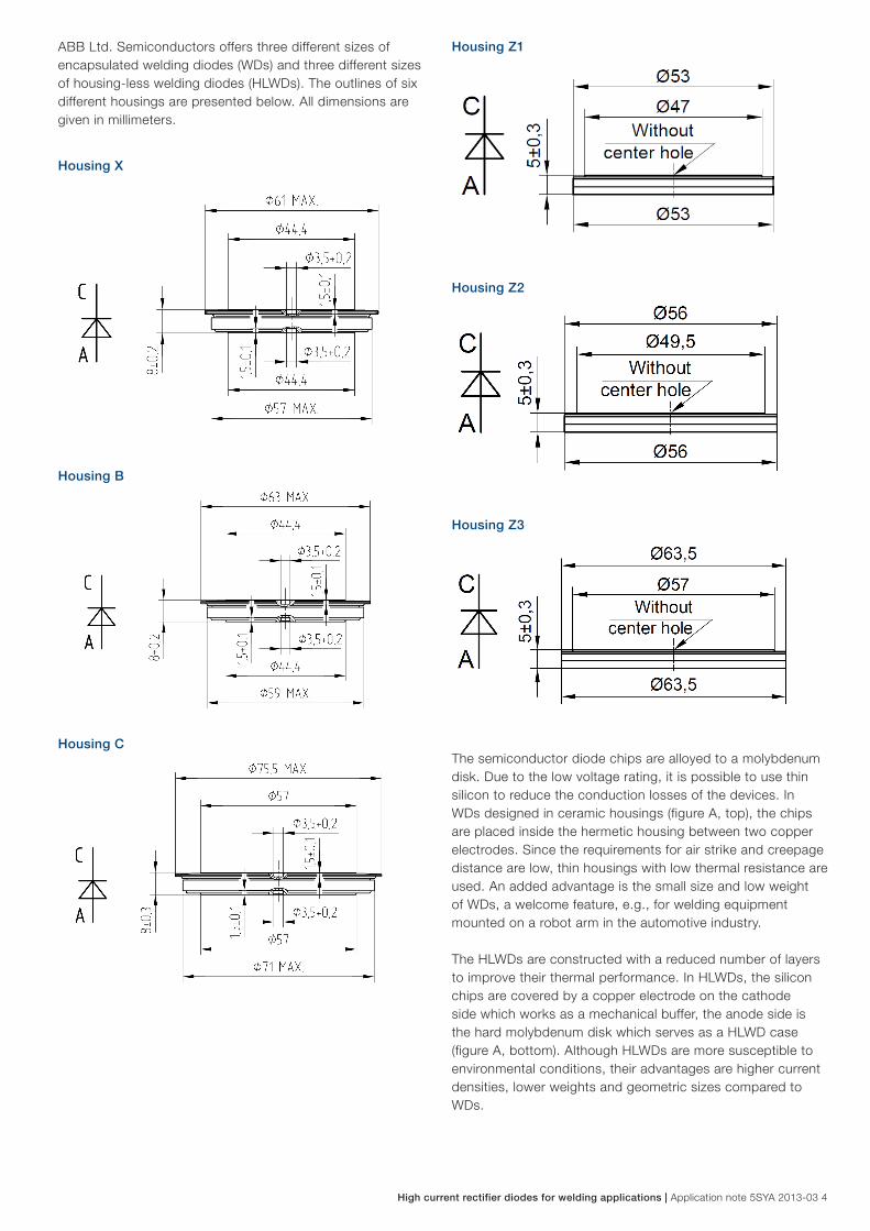
ABB Ltd. Semiconductors offers three different sizes of encapsulated welding diodes (WDs) and three different sizes of housing-less welding diodes (HLWDs). The outlines of six different housings are presented below. All dimensions are given in millimeters.
The semiconductor diode chips are alloyed to a molybdenum disk. Due to the low voltage rating, it is possible to use thin silicon to reduce the conduction losses of the devices. In WDs designed in ceramic housings (figure A, top), the chips are placed inside the hermetic housing between two copper electrodes. Since the requirements for air strike and creepage distance are low, thin housings with low thermal resistance are used. An added advantage is the small size and low weight of WDs, a welcome feature, e.g., for welding equipment mounted on a robot arm in the automotive industry.
The HLWDs are constructed with a reduced number of layers to improve their thermal performance. In HLWDs, the silicon chips are covered by a copper electrode on the cathode side which works as a mechanical buffer, the anode side is the hard molybdenum disk which serves as a HLWD case (figure A, bottom). Although HLWDs are more susceptible to environmental conditions, their advantages are higher current densities, lower weights and geometric sizes compared to WDs.
Housing X
Housing B
Housing C
Housing Z1
Housing Z2
Housing Z3

5 Application note 5SYA 2013-03 | High current rectifier diodes for welding applications
Figure A: the WD in the housing (at the top) and the HLWD (at the bottom).
The standard welding diodes can operate at frequencies up to 7 kHz. However, their optimal and reliable frequency range is up to 2 kHz. To meet the demands of higher frequencies up to 10 kHz, a new group of high frequency rectifier diodes with high current capabilities combined with excellent reverse recovery characteristics have been developed. The high fre-quency diodes are available both in sealed and housing-less versions.
2. Data sheet user guideThe aim of this section is to guide readers through the welding diode data sheet to understand it properly. The various device parameters which appear in the data sheet are defined and their dependencies are supported by figures where it is appro-priate. For explanation purposes, data and diagrams associated with 5SDD 71B0400 are used. However, the guide is applicable to all product range of WDs and HLWDs (table 1). The parameters are defined according to the standard IEC 60747.
The key parameters determine the basic voltage and current ratings of the diode. The parameter values are followed by short descriptions of the main features of the welding diode.
2.1. Blocking
VRRM: the maximum allowable reverse voltage that may be applied to the diode repetitively. The diode must be operated at or below VRRM. Above this level the device will thermally “run-away” and become a short circuit. The rating of VRRM is valid across the full operation temperature range of the diode. The parameter is measured with 10 ms half-sine pulses and a repe-tition frequency of 50 Hz
IRRM: the maximum repetitive reverse leakage current given at specified conditions
Maximum ratings Maximum
limits
Unit
VRRM Repetitive peak
reverse voltage
5SDD 71B0400 400 V
Tj = -40 ÷ 170 °C 5SDD 71B0200 200
IRRM Repetitive
reverse current
50 mA
VR = VRRM

High current rectifier diodes for welding applications | Application note 5SYA 2013-03 6
2.2. Mechanical
The mechanical part of the data sheet includes the outline drawing of the diode housing where all dimensions are in millimeters, and represent various nominal mechanical parameters.
FM: the recommended mounting force applied to the device in order to establish the contact pressure for its optimal performance. An application of a lower mounting force leads to an increase of the device thermal impedance and junction temperature excursion, correspondingly. It reduces the diode operation time. On the contrary, an application of higher clamping force may crack the wafer during the load cycling
m: the device weight in kilograms
Ds: the surface creepage distance is the shortest path along the housing between the anode and cathode
Da: the air strike distance is the shortest direct path between the anode and cathode
2 3. On-state
Maximum ratings Maximum limits Unit
IFAVm
Average forward current
TC = 85°C
7 110A
IFRMS
RMS forward current
TC = 85°C
11 200A
IR
Repetitive reverse current
VR = VRRM
50mA
IFSM
Nonrepetitive peak surge current
tp = 10 ms, VR = 0 V, half sine pulse
55 000A
I2tLimiting load integral
tp = 10 ms, VR = 0 V, half sine pulse
15 125 000A2s
Tjmin –Tjmax Operating temperature range - 40 ÷ 170 °C
Tstgmin – TstgmaxStorage temperature range - 40 ÷ 170 °C
Figure 1: Case
Unless otherwise specified Tj = 170 °C

7 Application note 5SYA 2013-03 | High current rectifier diodes for welding applications
IFAVM: the maximum allowable average forward current IFRMS: the maximum allowable root mean square (RMS) forward current
IFAVM and IFRMS are defined for 180 ° sine wave pulses of the 50 % duty cycle at the case temperature, TC.
IFSM: the maximum allowable non-repetitive peak forward surge current
∫I2dt: the integral of the square of the current over a defined period
IFSM and ∫I2dt are determined for a half sine-wave current pulse without a reapplied voltage, VR = 0. Above the specified values, the device will fail short-circuit. Both parameters are required for protection coordination. The values are introduced for two pulse lengths corresponding to the line frequencies 50 and 60 Hz. In welding applications, however, both the load and fault currents are almost the same and are determined by trans-former impedance such that surge capability is seldom of great interest. The dependence of IFSM and ∫I2dt on the single half sine pulse duration at Tjmax is shown in figure 4 of the data sheet example.
VFM: the maximum forward voltage drop of the diode at given conditions
Characteristics Value Unit
min typ max
VT0 Threshold voltage 0.740 V
rT Forward slope resistance
IF1 = 5 000 A, IF2 = 15 000 A
0.026 mΩ
VFM Maximum forward voltage
IFM = 5 000 A, Tj = 25 °C
1.05 V
The threshold voltage, VT0, and the slope resistance, rT, allow a linear representation of the diode forward voltage drop, and are used to calculate conduction losses of the device, PT. For a given current, the conduction losses can be calculated using equation 1:
,** 20 FRMSTFAVTT IrIVP += Eq. 1
where IFAV and IFRMS are parameters described above. To mini-mise losses, VT0 and rT should be as low as possible. Note, that the linear approximation of the on-state voltage characteristic (see figure 3 of the data sheet example) is valid only within given current limits. Outside these limits, the on-state curve is not linear, and it is preferable to use more complicated models to describe the non-linear shape of the on-state voltage characteristic.
Tj: the operating junction temperature
Tjmin - Tjmax: the operating junction temperature range describes the limits at which the device can be used. If the lim-its are exceeded, the device ratings are no longer valid and there is a risk of catastrophic failure
Tstgmin - Tstgmax: the maximum allowable temperature interval for short term storage of the diode without a transport box
For storage and transportation of the device in the transport box, see environmental specifications 5SZK9104 and 5SZK9105.
2 4. Thermal characteristicsThermal Specifications Value Unit
Rthjc Thermal resistance
junction to case
double side cooling 10 K/kW
single side cooling 20 K/kW
Rthch Thermal resistance
case to heatsink
double side cooling 5 K/kW
single side cooling 10 K/kW
Figure 2 The dependence of the transient thermal impedance junction to case on square pulse duration for the double side cooling

High current rectifier diodes for welding applications | Application note 5SYA 2013-03 8
Rthjc: the thermal resistance as measured from the diode’s junction to the baseplate of the diode’s case
Rthch: the thermal resistance as measured from the diode’s case to heat sink
The thermal resistances Rthjc and Rthch are measures of how well power losses can be transferred to the cooling system. The values are given for both cases, the double side cooling, where the device is clamped between two heat sinks, and single side cooling, where the device is clamped to a single heat sink only. The temperature rise of the “virtual junction” of the silicon wafer inside the diode in relation to the heat sink, ΔTjh, is given by equation 2.
Eq. 2
It is preferable that Rthjc and Rthch should be as low as possible since the silicon temperature determines the current capability of the diode. Furthermore, the temperature excursion of the silicon wafer determines the load-cycling capability and life expectancy of the diode.
Zthjc: the transient thermal impedance
Zthjc emulates a rise of the junction temperature in time when the power dissipation in the silicon junction is not constant. The dependence of Zthjc on the square pulse duration, td, in the case of double side cooling is shown in the figure 2 of the data sheet example. This function can be either specified as a curve or as an analytical function with the superposition of usually four exponential terms. The analytical expression is particularly useful for computer calculations and makes it possible to simulate the entire system from junction to ambient. The steady state value of Zthjc at td ≥ 1 s corresponds to Rthjc = 10 K/kW presented in the table of thermal specifications.
Figure 3: Maximum forward voltage drop characteristics. The on-state voltage drop of the diode, VF, as a function of the on-state current, IF, at given junction temperatures.
( )thchthjcTjh RRPT +=∆ *
0
2
4
6
8
10
12
14
16
18
20
0 0.5 1 1.5
I F( k
A )
VF ( V )
25 °CTj = 170 °C
2 5. Power loss and maximum case temperature characteristics
Inspite of that the 50-60 Hz forward current pulse period is not a typical operation condition for the welding diode, in this section we present characteristics of forward power losses, PT, calculated for 50 Hz, as these characteristics are considered as a standard and are used in power semiconductor datasheets. The diode load characteristics calculated for the most common welding diode application conditions are presented in sections 3 and 4. Figures 5 and 6 show forward power losses, PT, as a function of the average forward current, IFAV, for typical sine and square current wave forms. The curves are calculated, based on characteristics of the maximum forward voltage drop, VFM (IF), at Tjmax (which are demonstrated in figure 3) without considering any reverse recovery losses. The curves are valid only for the 50 or 60 Hz operation. Figures 7 and 8 describe the maximum permissible case temperature, TC, against the average forward current, IFAV, for typical sine and square current wave forms. The curves are calculated based on the thermal resistance for the double side cooling, for the specified current wave forms and at the maximum junction temperature, Tjmax.Power losses, PT, the ambient temperature, TA, given by the application, and the maximum case temperature, TC, obtained from figures 7 and 8, are used to calculate the diode junction to heat sink thermal resistance, Rthjh.
Figure 4: Surge forward current vs. pulse length, half sine wave, single pulse, VR = 0 V, Tj = Tjmax. The non-repetitive surge current limit, IFSM, and the surge current integral, ∫I2dt, for different widths of the half sine pulse at Tjmax.

9 Application note 5SYA 2013-03 | High current rectifier diodes for welding applications
Figure 6 Foward power loss vs. average foward current, square waveform,
f = 50 Hz
Figure 5 Foward power loss vs. average foward current, sine waveform,
f = 50 Hz
Figure 7 Maximum case temperature vs. average foward current, sine
waveform, f = 50 Hz
Figure 8 Maximum case temperature vs. average foward current, square
waveform, f = 50 Hz

High current rectifier diodes for welding applications | Application note 5SYA 2013-03 10
3. Load cycling capability and welding currentThe load cycling capability of the welding diodes is crucial for the choice of application components. Each welding cycle represents a load cycle for the diode used in the application. The load cycling capability is determined by the temperature swing the diode undergoes during the cycle. To keep the temperature swing as low as possible during the welding cycle, the diodes must be designed for lowest possible losses and thermal impedance.Usually, the standard diode specifications do not provide manufacturers with specific information on rectifier diodes useful for a correct rating of a welding machine operating at a given duty cycle and cooling conditions. The diode
lifetime dependence on the junction to heat sink temperature excursion, ∆Tjh, is an example of this data deficiency. Figure B demonstrates the number of load cycles as a function of ∆Tjh obtained experimentally in collaboration with welding equipment manufacturers. The dependence is valid for the whole welding diode product range. The lifetime curve indicates how many cycles it is possible to reach in case of right mounting and proper cooling of diodes under the test. Since the experiment is time consuming, the number of tested devices is limited. This fact could slightly affect the accuracy of the lifetime trend.
Figure B Achievable load cycling capability of welding diodes produced in ABB Ltd. Semiconductors, as a function of diode’s junction to heat
sink temperature excursion, ∆Tjh
3 1. The welding cycle and diode loadFigure C displays the common diagram of a diode rectifier in the welding application. The simplest connection is of the M2 type with one diode in each leg in order to reduce the number of diodes required for rectification. Since the welding quality is better when using DC instead of AC current, a welding diode rectifier is used to convert the square wave current (usually 1 kHz) to a DC current. In the automotive industry, a typical welding cycle period, T, consists the welding time, td, (typically several hundreds of milliseconds), and the rest time between welding intervals, with a total duration usually in the range of 1-10 seconds. The rest time between welding intervals includes the holding time,
gun opening time, gun moving time and gun closing time. The duty cycle, ED, is defined by the ratio:
Eq. 3
The welding sequence and definition of the duty cycle are shown in figure D.
1.E+03
1.E+04
1.E+05
1.E+06
1.E+07
1.E+08
0 20 40 60 80 100 120 140
∆Tjh ( °C )
num
ber o
f cyc
les

11 Application note 5SYA 2013-03 | High current rectifier diodes for welding applications
Figure C The diode rectifier diagram, the M2 connection
Based on the diagram in figure C, the average output DC current during the welding pulse, ID, is given by the expression
FAVD II 2= Eq. 4
where IFAV is the maximum average forward current defined in Section 2
Eq. 5
In equation 5, VF0 is a threshold voltage, rT is a forward slope resistance, FF is a form factor (FF2 = 2 for the rectangular pulse shape), and Pja is junction to ambient power loss
Eq. 6
which is determined by the difference of junction and ambient temperatures, ∆Tja, corresponding to the actual temperature rise during one full welding cycle (power “on” and “off”) and the transi-ent junction to ambient thermal impedance, Zthja. At high frequencies, the reverse recovery losses have to be accounted for. In figures 5, 6 the calculated dependencies do not include the recovery losses correction, as it is negligible for the 50-60 Hz ope-
ration. However, in the case of 1 kHz welding operation, the amount of reverse recovery losses is significant and the total for-ward power losses have to be reduced by 20 % in the calculation.
The total thermal impedance junction to ambient, Zthja, is defined by
Eq. 7
where the transient junction to heat sink impedance, Zthjh, is given in the form
Eq. 8
In equation 8, i is the summation index, td and T are the welding time and period, ti is a thermal time constant described in section 2 in the datasheet table of the diode thermal characteristics together with the junction to case thermal resistance, Rthjc. Rthjh
is the thermal resistance junction to heat sink obtained by a normalization of Rthjc to a saturated value of Rthch chosen for the double side cooling in our calculations.
∆Tja is calculated from the relation
Eq. 9
where ∆Tjh is a constant obtained from figure B for the desired number of temperature cycles, Rthha, is the resistance to heat flow as measured from the heat sink to ambient. The used Rthha of ~ 0.7 K/kW was obtained experimentally by measurements of the thermal resistance of common welding transformers in the M2 configuration.
3 2. Examples of welding curves for 5SDD 71B0400
Examples of dependencies of the welding current, ID, on the duty cycle, ED, for the 5SDD 71B0400 diode type are presented in the figure B. The welding curves are calculated for different temperature excursions, ∆Tjh = 40, 60, 70, 80 °C, and various welding pulse widths, td = 20, 40, 100, 2000, 1000 ms. As mentioned earlier, for a desired load cycling capability, i.e., the number of temperature cycles, the allowable temperature excursion, ∆Tjh, which represents the cooling system quality, can be estimated from figure B. After that the maximum allowable welding current, ID, can be determined for definite welding application parameters, such as the welding pulse width, duty cycle and junction temperature difference. For example, it is required to reach approximately 10 million cycles in the welding application with 5SDD 71B0400, from figure B we obtain an allowed ∆Tj = 60 °C. For 100 pulses (td = 100 ms) with ED = 10 %, the allowable welding current ID = 10 kA (see figure 9 for ∆Tj = 60 °C). In order to reach, with a good probability, the above specified load cycling
Figure D The definition of a duty cycle for a typical welding application
thhathjhthja ZZZ +=
i
ithjh
ithha
ithjhjh
ja R
RRTT
Zthjh = ∑ Rthjhi
i
(1 - e- tdτi
1 - e- Tτi
)

High current rectifier diodes for welding applications | Application note 5SYA 2013-03 12
Figure 9 Current load capacity, cont., DC output welding current with single-phase centre tap vs. duty cycle for different temperature
swings ∆Tjh, f = 1000 Hz, square wave
5
10
15
20
25
1 10 100
I D( k
A )
Duty cycle ED ( % )
100 ms
40 ms
1000 ms / DC
200 ms
td = 20 ms ∆Tjh = 80 °C
5
10
15
20
25
1 10 100
I D( k
A )
Duty cycle ED ( % )
100 ms
40 ms
1000 ms / DC
200 ms
td = 20 ms
∆Tjh = 70 °C
5
10
15
20
25
1 10 100
I D( k
A )
Duty cycle ED ( % )
100 ms
40 ms
1000 ms / DC
200 ms
td = 20 ms
∆Tjh = 60 °C
5
10
15
20
25
1 10 100
I D( k
A )
Duty cycle ED ( % )
100 ms
40 ms
1000 ms / DC
200 ms
td = 20 ms
∆Tjh = 40 °C
capability, the mechanical design criteria described in sections 3 and 5, must be met.In this application note, welding curves are calculated only for the case of the M2 connection (figure C) with the medium frequency (1 kHz) square wave form. Similar curves can be generated for other connections and wave forms upon request.
4. Correct welding diode installationThe mechanical design of the rectifier is crucial for its performance. An inhomogeneous pressure distribution is one of the most common reasons of diode failure in welding applications.
4 1. CoolingDue to the need for high power density encountered in welding applications, the water cooling is the only method used in practice, since other components of the welding system, as, e.g., welding guns, are almost always water-cooled. The cooling should be homogeneous over the whole diode contact surface. A single water channel through the center of the heat sink may not be sufficient for heavy-duty equipment and could lead to overheating of the diode rim. The employment of the cooling system with more complicated paths of water channels which would provoke better turbulence is advisable rather than using of simple straight paths (though it may be sufficient for light duty units).

13 Application note 5SYA 2013-03 | High current rectifier diodes for welding applications
4 2. Clamping and surface treatment
To acquaint with main recommendations related to the device mechanical design and surface treatment, read the document 5SYA2036. In addition to recommendations in 5SYA2036, it has to be mentioned that it is not essential to use thermal greases if the following conditions are fulfilled: • The heat sinks have a surface finish equal or better in
terms of roughness and flatness than those parameters of the diode
• Heat sinks are galvanically plated with silver-nickel, pure silver, gold or nickel
• The mounting pressure is homogeneously applied over the whole diode surface and kept stable in the required tolerance.
This recommendation does though not exclude the use of a thin film of a light grease or oil. The interface grease must be carefully chosen for its long-term chemical stability and corrosion inhibiting properties.
4 3. Additional considerations regarding the housingless welding diodes
The standard HLWDs, 5SDD xxZ0401, and high frequency HLWDs, 5SDF xxZ0401, do not have a hermetically sealed housing. Therefore, a special care must be taken during handling and operation of these diodes.
To minimize the environmental impact during transport and storage, HLWDs are delivered in a sealed foil. It is recommended to keep the diode in the foil, and store it at the conditions specified in the environmental specification 5SZK9104, until the device assembly.
The cathode side of the HLWD has a small copper pole piece that to some extent can act as a mechanical buffer. On the anode side, such buffer is missing since the high hardness molybdenum disc serves as a HLWD case. The molybdenum disc is usually connected directly to a hard copper heat sink. The molybdenum-copper interface has few possibilities to even out imperfections of the surface that leads to the reduction of tolerances regarding roughness and flatness in order to avoid an excessive voltage drop over the interface and fast deterioration of the interface during load cycling.
In addition to recommendations in the application notes 5SYA2036, the following advices should be considered when assembling the HLWD:• To protect the HLWD from particles and liquids, it is
recommended to seal the diode with an o-ring. It is recommended to use o-rings made from materials as Viton® due to their capability to withstand high temperatures and chemicals
• The anode and cathode of the HLWD do not have a centering hole. It means that the centering must be made on the device perimeter
• The HLWDs are susceptible to damage caused by particles, such as small shavings on the surface,
during load cycling. It can especially occur on the hard molybdenum anode side. Therefore, the assembly should not be carried out in work shop areas where metal is being machined, but in separated places in order to avoid particles to attach to the diode surface.
5. Other application aspects5.1. Parallel connectionWhen an application needs higher currents, the capability can be increased by using two or more diodes connected in parallel. Welding diodes made by ABB Ltd. Semiconductors can be connected in parallel, but it requires a good symmetric design and accurate mounting to avoid the need for the considerable de-rating of the current through each diode. Even at good conditions a minimum de-rating of ~ 10 % is recommended such that each diode is utilized to a maximum of 90 % of its capability. This precaution is suggested because there will always be small asymmetries in the transformer connections and the voltage drop in the interfaces will always have some spread. These inherent asymmetries give rise to an unequal current sharing between devices causing different losses in the diodes. It can lead to device overheating and lower reliability than expected.
The 400 V device types, 5SDD 71X0400 and 5SDD 0120C0400, have better adaptation for a parallel connection, as they have a reduced voltage drop spread in comparison with 5SDD 71X0200 and 5SDD 0120C0200 versions. We do not recommend to use HLWDs for the parallel operation due to their especial properties described in section 5.2.
Returning back to the earlier example with 5SDD 71B0400, if the application needs to approach 10 million cycles that brings the maximum temperature excursion ∆Tjh = 60 °C, and the allowable welding current calculated for the regime of 100 ms with a duty cycle of 10 % is 10 kA. Thus, in order to reach 10 million cycle capability using two diodes in parallel, the equipment rating must not exceed 2 * 0.9 * 10 kA = 18 kA.
5.2. Welding diode turn-off behaviourThe turn-off behaviour of the diode is of relevance to the welding equipment design even if the supply voltage is only in the range of 6 – 20 V. Since the diodes are used without any voltage protection such as an RC-circuit, a device with a “snappy” turn-off behaviour can generate excessive voltage spikes and destroy itself.
The diodes from ABB Ltd. Semiconductors are designed to have a soft turn-off that does not generate voltage spikes in excess of its capability. Figure E shows the typical turn-off wave form of a welding diode measured at normal operating conditions with the commutation voltage VR = 15 V in the M2 configuration. For the normal operation it is important to keep the spike voltage below the rated voltage of the device. In the typical example in figure E, the diode generates an overvoltage of about 80 V which is less than the diode voltage class with big reserves.

14 AD/RandC/010–EN | ControlMaster CM10, CM30 and CM50 | Universal process controllers, 1/8, 1/4 and 1/2 DINHigh current rectifier diodes for welding applications | Application note 5SYA 2013-03 14
Figure E The typical turn-off wave form of the welding diode at
VR = 15 V
5.3. Welding diode operation at high frequency
The standard welding diodes produced in ABB Ltd. Semiconductors have been originally designed for operations at line frequencies, but their soft turn-off behaviour makes them well suited for operations at medium frequencies. Today our diodes are mainly utilized at frequencies up to 2 kHz. This frequency range was used for measurements presented in the capability curve in figure B.
ABB Ltd. Semiconductors high frequency welding diodes can be employed in applications with switching frequencies up to 10 kHz (e.g., for aluminium welding) with good results. At frequencies higher than 2 kHz the high frequency weldingdiodes still have high current capabilities. The average forward current, IFAV, dependences on the frequency, f, are shown in figure F in order to compare the standard and high frequency diodes. It is evident that in the case of standard diodes, the average forward current starts to drop at frequencies ~ 2 kHz as a consequence of the reverse recovery losses growth. The higher frequency diodes with their guaranteed reduced reverse recovery charge, Qrr, and short life time of minority carriers, obtained by the electron irradiation technology, gain low reverse recovery losses at the same frequencies. To calculate the welding currents for high frequency diodes, as described in section 3.1, the coefficient of the total forward power losses reduction can be estimated from figure F (bottom).
0
5000
10000
15000
10 100 1000 10000
I FAV
( A )
f ( Hz )
180°
270°
120°
90°
60°
ψ = 30°
0
5000
10000
15000
10 100 1000 10000
I FAV
( A )
f ( Hz )
180°
270°
120°90°
60°
ψ = 30°
Figure F The average forward current vs. frequency for the standard 5SDD
92Z0400 (top) and high frequency 5SDF 90Z0401 (bottom) welding diodes,
trapezoid waveform, TC = 85 °C, diF/dt = ± 2 000 A/µs, VR = 50 V.

Ap
plic
atio
n no
te 5
SYA
201
3-03
6. References[1] IEC 60747 “Semiconductor devices”[2] 5SYA2036 “Recommendations regarding mechanical clamping of high power press-pack semiconductors”[3] 5SZK9104 “Specification of environmental class for pressure contact diodes, PCTs and GTOs, storage”[4] 5SZK9105 “Specification of environmental class for pressure contact diodes, PCTs and GTOs, transportation”
7. Revision history
Note
We reserve the right to make technical changes or
to modify the contents of this document without
prior notice.
We reserve all rights in this document and the infor-
mation contained therein. Any reproduction or
utilisation of this document or parts thereof for
commercial purposes without our prior writtencon-
sent is forbidden.
Any liability for use of our products contrary to the
instructions in this document is excluded.
ABB Switzerland Ltd.SemiconductorsFabrikstrasse 3CH-5600 LenzburgSwitzerlandTel: +41 58 586 14 19Fax: +41 58 586 13 06E-Mail: [email protected]/semiconductors
Version Change Authors
03 Björn Backlund
Ladislav Radvan
Nataliya Goncharuk