Application Note 1645 LM4702 Driving a MOSFET …application-notes.digchip.com/006/6-8904.pdfLM4702...
24
LM4702 Driving a MOSFET Output Stage National Semiconductor Application Note 1645 Troy Huebner May 2007 Introduction This application note provides supporting design information regarding National Semiconductor’s newest offering of high- performance, ultra high-fidelity audio amplifier driver ICs. The LM4702 and its derivatives provide a highly reliable, fully integrated, ultra high-end input stage solution for audio power amplifiers. The LM4702’s wide-bandwidth, fully-complemen- tary bipolar design enables superior distortion performance throughout the audio spectrum. Its ±100V operating voltage range allows for power levels up to 450W into 8Ω and 900W into 4Ω. This unique IC solution provides a quick and easy way to manufacture an ultra high-fidelity amplifier solution, with the piece-of-mind obtained from a fully optimized, stable design. The LM4702 is available in two grades of performance. The C version has an operating voltage up to ±75V, while the B version operates up to ±100V. The LM4702 is available in National’s 15 lead TO-220 non-isolated power package. Ad- ditional topics regarding the LM4702 can be found in other application notes as stated below: AN-1490 LM4702 POWER AMPLIFIER AN-XXXX COMPENSATING & OPTIMIZING THE LM4702 AN-XXXX LM4702 OUTPUT STAGE INFORMATION AN-1645 LM4702 DRIVING A MOSFET OUTPUT STAGE Overview This application note will cover the design of a 2x125W, 8Ω with ≤ 1% THD+N amplifier solution using the LM4702 di- rectly driving an output stage that uses a complimentary pair of MOSFETs. Basic information on how to choose a suitable MOSFET device, setting bias levels, performance optimiza- tions, and performance results will be covered. The complete test schematic is included. The choice of device type and the design of the output stage of a power amplifier are determined by the design require- ments and the preference of the designer. A MOSFET device has some preferred features compared to a BJT device. MOSFETs do not suffer from second breakdown allowing the safe operating area (SOA) protection circuitry design to be less complicated. Thermal runaway issues are also much less of a concern with less sensitivity to temperature than a BJT device. MOSFET devices do not have charge storage (mi- nority carriers) reducing switch-off distortion effects. Some just prefer the sound of a MOSFET output stage compared to other devices, a highly subjective criteria but one that is im- portant in the evaluation of an amplifier's performance. How To Choose A MOSFET The choice of the MOSFET device is limited by the charac- teristics of the LM4702. The most important limitation is the bias voltage typical of 6V between the SINK and SOURCE pins. This voltage is also the voltage from Gate/Base to Source/Emitter (V GS or V BE ) of both devices in the output stage and any degeneration resistors. This limitation restricts MOSFET type to those with a V T low enough to allow proper bias and performance. A MOSFET device with high threshold voltage cannot be biased correctly and crossover distortion will dominate. For correct biasing the MOSFET must fully conduct at a minimum drain current of 100mA with a V GS of 3V or less. The MOSFET should be able to supply all the necessary output current at V GS = 10V with some headroom. The required output current is 5.6A peak for a 125W/8Ω out- put. The device needs to be able to supply more than 5.6A with a V GS of less than 10V. The other performance constraint of the LM4702 is the mini- mum guaranteed output drive current of 3mA (5.5mA typical). Although an additional driver stage can be employed to re- move the LM4702's drive current limitation, the design in this note will be done with the LM4702 driving the output stage directly. Devices with lower input capacitance are preferred but are not critical to a well performing design. The amount of drive current from the LM4702 limits the number of devices in parallel that can be driven with a acceptable slew rate. Addi- tional devices in parallel will not be covered in this note. An obvious drawback of driving a MOSFET output stage com- pared to a BJT output stage with the LM4702 is the loss of voltage swing relative to the supply rails. Unless the LM4702 is driven from higher supply rails, the maximum voltage swing with a MOSFET output stage may be lower than a BJT output stage. This is a result of the difference in V GS compared to V BE . The difference in output swing can be minimized through MOSFET selection and the elimination of degeneration re- sistors. The MOSEFET devices listed in Table 1 below are devices from three suppliers that will meet the design criteria based on the LM4702 limitations for direct drive and the target output power specification into a resistive load. The table is not an exhaustive listing but represents those devices which are commonly used in MOSEFET amplifier designs, were avail- able at the time of writing, and provide good audio perfor- mance. All devices listed have a 140V minimum break down voltage rating (V DSS ) or higher and drain current (I D ) maximum of 7A or higher. The V DSS and the I D are the requirements to meet the supply voltage and output current specifications with some headroom to spare. The Drain Current verses Gate to Source Voltage graph (I D vs. V GS ) is used to determine if cor- rect bias can be achieved with 3V or less. This design and device selections may not be suitable for all speaker loads without violating the device's Safe Operating Area (SOA) curves. Proper SOA design must be taken into account for a commercial amplifier product. © 2007 National Semiconductor Corporation 300232 www.national.com LM4702 Driving a MOSFET Output Stage AN-1645
Transcript of Application Note 1645 LM4702 Driving a MOSFET …application-notes.digchip.com/006/6-8904.pdfLM4702...

LM4702 Driving a MOSFETOutput Stage
National SemiconductorApplication Note 1645Troy HuebnerMay 2007
IntroductionThis application note provides supporting design informationregarding National Semiconductor’s newest offering of high-performance, ultra high-fidelity audio amplifier driver ICs.
The LM4702 and its derivatives provide a highly reliable, fullyintegrated, ultra high-end input stage solution for audio poweramplifiers. The LM4702’s wide-bandwidth, fully-complemen-tary bipolar design enables superior distortion performancethroughout the audio spectrum. Its ±100V operating voltagerange allows for power levels up to 450W into 8Ω and 900Winto 4Ω.This unique IC solution provides a quick and easy way tomanufacture an ultra high-fidelity amplifier solution, with thepiece-of-mind obtained from a fully optimized, stable design.
The LM4702 is available in two grades of performance. TheC version has an operating voltage up to ±75V, while the Bversion operates up to ±100V. The LM4702 is available inNational’s 15 lead TO-220 non-isolated power package. Ad-ditional topics regarding the LM4702 can be found in otherapplication notes as stated below:
AN-1490 LM4702 POWER AMPLIFIER
AN-XXXX COMPENSATING & OPTIMIZING THE LM4702
AN-XXXX LM4702 OUTPUT STAGE INFORMATION
AN-1645 LM4702 DRIVING A MOSFET OUTPUT STAGE
OverviewThis application note will cover the design of a 2x125W, 8Ωwith ≤ 1% THD+N amplifier solution using the LM4702 di-rectly driving an output stage that uses a complimentary pairof MOSFETs. Basic information on how to choose a suitableMOSFET device, setting bias levels, performance optimiza-tions, and performance results will be covered. The completetest schematic is included.
The choice of device type and the design of the output stageof a power amplifier are determined by the design require-ments and the preference of the designer. A MOSFET devicehas some preferred features compared to a BJT device.MOSFETs do not suffer from second breakdown allowing thesafe operating area (SOA) protection circuitry design to beless complicated. Thermal runaway issues are also much lessof a concern with less sensitivity to temperature than a BJTdevice. MOSFET devices do not have charge storage (mi-nority carriers) reducing switch-off distortion effects. Somejust prefer the sound of a MOSFET output stage compared toother devices, a highly subjective criteria but one that is im-portant in the evaluation of an amplifier's performance.
How To Choose A MOSFETThe choice of the MOSFET device is limited by the charac-teristics of the LM4702. The most important limitation is thebias voltage typical of 6V between the SINK and SOURCEpins. This voltage is also the voltage from Gate/Base toSource/Emitter (VGS or VBE) of both devices in the outputstage and any degeneration resistors. This limitation restrictsMOSFET type to those with a VT low enough to allow properbias and performance. A MOSFET device with high thresholdvoltage cannot be biased correctly and crossover distortionwill dominate. For correct biasing the MOSFET must fullyconduct at a minimum drain current of 100mA with a VGS of3V or less. The MOSFET should be able to supply all thenecessary output current at VGS = 10V with some headroom.The required output current is 5.6A peak for a 125W/8Ω out-put. The device needs to be able to supply more than 5.6Awith a VGS of less than 10V.
The other performance constraint of the LM4702 is the mini-mum guaranteed output drive current of 3mA (5.5mA typical).Although an additional driver stage can be employed to re-move the LM4702's drive current limitation, the design in thisnote will be done with the LM4702 driving the output stagedirectly. Devices with lower input capacitance are preferredbut are not critical to a well performing design. The amount ofdrive current from the LM4702 limits the number of devices inparallel that can be driven with a acceptable slew rate. Addi-tional devices in parallel will not be covered in this note.
An obvious drawback of driving a MOSFET output stage com-pared to a BJT output stage with the LM4702 is the loss ofvoltage swing relative to the supply rails. Unless the LM4702is driven from higher supply rails, the maximum voltage swingwith a MOSFET output stage may be lower than a BJT outputstage. This is a result of the difference in VGS compared toVBE. The difference in output swing can be minimized throughMOSFET selection and the elimination of degeneration re-sistors.
The MOSEFET devices listed in Table 1 below are devicesfrom three suppliers that will meet the design criteria basedon the LM4702 limitations for direct drive and the target outputpower specification into a resistive load. The table is not anexhaustive listing but represents those devices which arecommonly used in MOSEFET amplifier designs, were avail-able at the time of writing, and provide good audio perfor-mance. All devices listed have a 140V minimum break downvoltage rating (VDSS) or higher and drain current (ID) maximumof 7A or higher. The VDSS and the ID are the requirements tomeet the supply voltage and output current specifications withsome headroom to spare. The Drain Current verses Gate toSource Voltage graph (ID vs. VGS) is used to determine if cor-rect bias can be achieved with 3V or less. This design anddevice selections may not be suitable for all speaker loadswithout violating the device's Safe Operating Area (SOA)curves. Proper SOA design must be taken into account for acommercial amplifier product.
© 2007 National Semiconductor Corporation 300232 www.national.com
LM
4702 D
rivin
g a
MO
SF
ET
Ou
tpu
t Sta
ge
AN
-1645

TABLE 1.
Device Pair Manufacturer
2SK1057 / 2SJ161 Renesas
2SK1058 / 2SJ162 Renesas
BUZ900 / BUZ905 Magnatec
BUZ901 / BUZ906 Magnatec
2SK1529 / 2SJ200 Toshiba
2SK1530 / 2SJ201 Toshiba
IRFP240 / IRFP9240 International Rectifier
Only one pair from each supplier, the higher voltage or highercurrent versions, will be tested with performance curves. Inaddition, an example of high VT devices, the popular Interna-tional Rectifier IRFP240/IRFP9240 pair, is also shown.Crossover distortion is the dominant distortion, yet this per-formance may be acceptable for some market segments.
MOSFET Amplifier DesignFigure 1 shows the basic block diagram of an amplifier usingthe LM4702. The amplifier consists of three building blocks,the LM4702, the bias stage, and the output stage (there areno protection circuits). Each stage will be covered in detail.The power supply design will not be covered as a basic un-regulated supply consisting of a transformer, a bridge rectifier,with noise and reservoir capacitors is well known and com-mon.
30023210
FIGURE 1. Amplifier Block Diagram
The LM4702 is a high voltage driver that includes the inputstage and voltage amplifier stage (VAS) of a power amplifier.The LM4702, with feedback from the output stage, sets thegain and is externally compensated to set the slew rate. Theoutputs of the LM4702 drive the top and bottom sides of thebias and output stages. The LM4702 performance details arelimited to basic recommendations on ranges for gain, slewrate, and the component types that achieve the best perfor-mance.
The bias stage performs two functions. First, it sets the DCbias voltage and resulting bias current in the output stage forClass A, AB or B operation. Second, it allows thermal com-pensation that maintains steady bias current as the outputstage devices vary in temperature. As will be shown, certaindevices do not need temperature compensation and the biasstage becomes as simple as a resistor. Other devices willneed thermal tracking and temperature compensation con-trolled by the bias stage.
The output stage is a basic Source-Follower stage using asingle pair of complementary N-channel and P-channel tran-sistors for simplicity. The same output stage design will beused for all devices listed in Table 1.
LM4702 StageThe LM4702 operates similar to an op amp. The circuit shownin Figure 2 is a non-inverting configuration. Resistors Ri andRF set the gain to AV = 1+ RF/Ri (V/V). The Ci capacitor setsDC gain to unity and the low frequency response by creating
a high-pass filter with a -3dB point at f-3dB = 1/(2πCi Ri ) (Hz).For sonic quality, the design does not use an AC coupling,DC blocking capacitor. The CN capacitor shunts high frequen-cy noise present at the input to ground. The compensationcapacitor, CC, sets the slew rate and phase margin to ensureoscillation-free operation.
30023212
FIGURE 2. LM4702 Stage
The following are general recommendations for the LM4702stage.
1.) Set the gain in the range of 10V/V to 50V/V using low val-ues of metal film resistors for lowest noise. A gain of 30V/Vwill give excellent results.
2.) Use a heat sink for the LM4702. For best results, the heatsink temperature should not rise above 55ºC.
3.) The values of the gain setting resistors and the input re-sistors should be equal. RS = RF, RIN = Ri. RS should not beset too low as to cause loading of the source. Setting the re-sistors to equal values in the associated pairs ensures thatthe input bias currents will have negligible effect on the inputoffset voltage.
4.) Use a silver mica type capacitor for the compensation ca-pacitors, CC capacitors on the COMP pins, placed close tothe LM4702.
5.) The slew rate should be set to the highest possible whilemaintaining stability through the power and frequency rangesof operation.
6.) DC blocking input capacitors affect the low frequency re-sponse and their value must be chosen accordingly. An ad-ditional film capacitor used in parallel may improve the sonicquality. Eliminating the input capacitor will give the best sonicperformance.
7.) The feedback capacitor, Ci, sets the gain at DC to unityand also affects the low frequency response in relation to thevalue of the Ri resistor. This capacitor's value should be set
www.national.com 2
AN
-1645

using the same recommendations given to selecting the inputcapacitor's value.
8.) The input noise capacitor, CN, is used to filter high fre-quency noise that may be present on the input signal. Thiscapacitor may be any type and the value is typically 15pF -47pF.
9.) Supply bypassing and PCB design each have a significanteffect on harmonic distortion levels. Large value currentreservoir capacitors in parallel with smaller film capacitors arerecommend at the power supply and at the PCB supply ter-minals. In addition, film capacitor bypassing is recommendedat each supply pin of each active device.
Bias StageThis section will cover two different bias stages; a basic, non-temperature compensated bias design and one with thermaltracking and temperature compensation. Whether Class A,Class AB or Class B, the level of bias voltage is independentof the bias stage design.
A non-compensated design involves a simple resistor (or po-tentiometer for easy bias adjustment) and a capacitor. Figure3 shows the simple bias stage design. The additional resistor,RB2, is used to set a minimum bias voltage while the poten-tiometer is used to adjust the bias level as desired. CBIAS maybe more than one capacitor, such as the parallel combinationof a high value (μF) electrolytic with a small value (pF) filmtype capacitor. RBG helps to reduce the 2nd harmonic.
30023215
FIGURE 3. Resistor Bias Stage
For thermal tracking with temperature compensation, the veryuseful VBE multiplier is used as shown in Figure 4.
30023216
FIGURE 4. Resistor Bias Stage
A VBE multiplier works by using the voltage across the Base-Emitter junction of a BJT transistor, Q1, to set the bias voltage.The RB2 resistor and RPOT potentiometer are in parallel withthe VBE voltage of Q1. Using Ohm's Law, the current throughRB2 and RPOT will be:
I = VBE / (RB2 + RPOT) (A)
Ignoring the small amount of current that flows into the baseof Q1, this same current flows through RB1. Using Ohm's Lawagain, the voltage across RB1 is equal to:
VB1 = RB1 * I (V)
The total bias voltage is equal to the Collector to Emitter volt-age, VCE, of Q1, which is also the same as the voltage acrossRB1, RPOT, and RB2. Combining the voltage across RB2 andRPOT, which is the same as the VBE voltage of Q1, and thevoltage found above across RB1 results in Equation 1 below.
VBIAS = VCE = RB1 * I + VBE (V) (1)
Substituting for the current, I, results in Equation 2.
VBIAS = RB1 * [VBE/(RB2 + RPOT)] + VBE (V) (2)
Simplifying and arranging results in the well known VBE mul-tiplier equation shown in Equation 3.
VBIAS = VBE * [1 + RB1/(RB2 + RPOT)] (V) (3)
3 www.national.com
AN
-1645

As can be seen, the bias voltage will track the VBE voltage ofQ1 at a fixed ratio. The bias voltage will change with temper-ature when Q1 is mounted to the same heat sink as the outputdevices. The thermal feedback and temperature compensa-tion works as follows. For a given bias voltage, the outputstage's bias current will increased as the temperature in-creases. However, since Q1 is mounted along side the outputdevices, its (Figure 4) VBE voltage will decrease with in-creased temperature. This reduces the current through resis-tors connected to Q1's base, which results in a reduction ofbias voltage. This negative feedback produces a bias voltagethat changes in order to maintain a stable bias current in theoutput stage.
DETERMINING OUTPUT STAGE BIAS CURRENT
For a Class AB amplifier design, bias current is chosen suchthat crossover distortion is minimized while also keeping qui-escent power dissipation low. Higher bias current reducesharmonic distortion levels. At some point there is little reduc-tion with increased bias current and resulting power dissipa-tion. A tradeoff in the bias current level must be made betweenTHD performance and power dissipation.
MOSFET output stages typically need higher bias currentthan BJT output stages for good performance in a Class ABamplifier design. Using the Magnatec BUZ901/BUZ906 pairand the resistor bias circuit shown in Figure 3, different biascurrent levels are shown in the FFT versus Frequency graphsand oscilloscope photos (Figures 5 - 10). For each graph theoutput power level is 40W into an 8Ω resistive load. The mea-surement equipment is set to notch out the fundamentalfrequency of the test signal. The fundamental is reduced bymore than -110dB relative to 0dB. 0dB is set equal to the volt-age for 40W into 8Ω. The first graph, Figure 5, has a biascurrent of 50mA and shows a case of insufficient bias current.The result is THD that is dominated by crossover distortion.This is indicated by the high level and number of harmonics.Figure 6 shows the residual harmonics on an oscilloscopeand clearly crossover distortion is dominant.
30023240
FIGURE 5. 50mA Bias Current
30023220
FIGURE 6. 50mA Bias Current
Increasing the bias current to 150mA reduces the magnitudeof the harmonics as shown in the FFT of Figure 7 and theoscilloscope view in Figure 8.
30023229
FIGURE 7. 150mA Bias Current
30023218
FIGURE 8. 150mA Bias Current
www.national.com 4
AN
-1645

Figures 9 and 10 show the harmonic content when the biasis pushed all the way to 500mA.
30023239
FIGURE 9. 500mA Bias Current
30023219
FIGURE 10. 500mA Bias Current
Figures 11 through 13 show the difference in harmonics withbias levels of 100mA, 200mA and 300mA using the MagnatecBUZ901/BUZ906 pair. Similar results using the same biascurrent levels can be observed with any of the devices listedin Table 1.
30023228
FIGURE 11. 100mA Bias Current
30023237
FIGURE 12. 200mA Bias Current
30023238
FIGURE 13. 300mA Bias Current
Tables 2 - 4 list the resulting 1kHz THD+N measurement at40W into an 8Ω load with a 22kHz measurement bandwidth.
5 www.national.com
AN
-1645

The tables show that bias currents above 200mA produceonly minor improvements in THD+N at a significant powerdissipation cost.
TABLE 2. Magnatec Bias Current and THD+N
Bias Current1kHz THD+N at 40W/8Ω
Single Channel, 22kHz BW
50mA 0.00129%
100mA 0.00104%
150mA 0.00085%
200mA 0.00068%
250mA 0.00064%
300mA 0.00062%
1A 0.00061%
TABLE 3. Renesas Bias Current and THD+N
Bias Current1kHz THD+N at 40W/8Ω
Single Channel, 22kHz BW
50mA 0.00129%
100mA 0.00098%
150mA 0.00081%
200mA 0.00074%
250mA 0.00070%
300mA 0.00068%
1A 0.00075%
TABLE 4. Toshiba Bias Current and THD+N
Bias Current1kHz THD+N at 40W/8Ω
Single Channel, 22kHz BW
50mA 0.00085%
100mA 0.00070%
150mA 0.00067%
200mA 0.00064%
250mA 0.00061%
300mA 0.00057%
1A 0.00055%
The graphs above and information in Tables 2- 4 indicate thatthe a range of 100mA to 200mA of bias current in the outputstage produces low magnitude harmonics and manageablepower dissipation.
Because of the higher VT the IRFP240/IRFP9240 pair cannotbe biased correctly to eliminate crossover distortion and THDperformance will be affected. The maximum bias voltage ob-tained was 7.1V with no resistor between the SINK andSOURCE pins of the LM4702 (A 20kΩ resistor may be usedwith the bias voltage reduced to 7V). The bias current is 25mAunder these conditions. Figure 14 below shows the THDresidual on an oscilloscope indicating crossover distortion isdominant.
30023275
FIGURE 14. 40W Output and THD Residual
DETERMINING BIAS CIRCUIT DESIGN
Device characteristics and design goals determine whetherthermal tracking is needed for stable bias current over tem-perature. To determine which devices need thermal trackingand which do not, the Drain Current verses Gate - Sourcevoltage (ID vs. VGS) graph in the device datasheet can beused. Device manufacturers typically have multiple plots onthe ID - VGS graph for different case temperatures. The inter-section point of the plots is where stable bias current can beachieved at a fixed bias voltage and without thermal tracking.At higher or lower VGSvoltages, the drain current will vary withcase temperature.
Inspection of the graphs for the Renesas 2SK1058/2SJ162pair and the Magnatec BUZ901/BUZ906 pair shows that threedifferent case temperature plots all intersect at low drain cur-rent (<0.5A). The Toshiba 2SK1530/2SJ201 pair and Inter-national Rectifier IRFP240/IRFP9240 pair graphs have anintersection of the three plots at a very high drain current(>5A). In fact, the 2SJ201 does not appear to have an inter-section point on the graph. From these graphs it is determinedthat the Renesas and Magnatec pairs can be biased in the100mA to 200mA range previously determined without theneed for thermal tracking. A simple bias resistor circuit willgive stable bias current over operating temperature.
The Toshiba 2SK1530/2SJ201 pair will require the VBE mul-tiplier circuit for thermal tracking with temperature compen-sation to achieve stable bias current over temperature. A biaslevel of 150mA in the output stage will be used for the2SK1530/2SJ201 pair.
The IRFP240/IRFP9240 would need thermal tracking if prop-erly biased since the intersection point on the ID - VGS is athigh current. The limitation in bias voltage with the LM4702does not allow for proper bias.
It may be desirable to have higher bias current to reduce dis-tortion harmonics, improve THD performance, affect sonicqualities, or some other design criteria. High bias current lev-els can be set with a simple resistor bias design. The tradeofffor simplicity is more bias variation over case temperature.The amount of variation can be determined using the device'sID - VGS graph. Depending on the device and design goal, theamount of variation may be acceptable at a higher bias level.For example, the Renesas 2SK1058/2SJ162 devices couldbe biased at 250mA without temperature compensation. Thebias current will vary much more than if the bias is set at theintersection point but the amount of variation may be accept-able. If bias stability is not acceptable then additional circuitrywill be required for temperature compensation. Devices likethe Toshiba 2SK1530/2SJ201 pair are not well suited for a
www.national.com 6
AN
-1645

resistor bias (fixed bias voltage) scheme because the currentwill significantly vary with case temperature. The effects ofbias instability on sonic performance is not investigated in thisapplication note.
BIAS STABILITY
The Bias Current versus Time graphs below were created byrunning the output stage at 40W until steady state case andheat sink temperature are reached. The input signal is turnedoff (Time = 0) and the bias current recorded over time. Itshould be noted that the graph units are not linear as indicat-ed. Bias current is measured at 10 second intervals for thefirst two minutes after the input signal was turned off then at30 second intervals up to five minutes. One final measure-ment is taken at 10 minutes. The time steps are one reasonfor the different slopes on the time curve, more evident on thehigher bias graphs. There are two plots on each graph, oneindicating the quiescent steady state bias and the other indi-cating the bias over time after producing 40W of output power.There are several factors that affect the data such as θJC ofthe package and heat sink size which contribute to thermaldelay. Device characteristics also affect the slopes of the timecurves.
Figure 15 is the Renesas 2SK1058/2SJ162 pair operating ata bias of 100mA for the output stage in quiescent steady state.The power test shows a slightly higher bias when the devicesare hot indicating that increasing the quiescent steady statebias would reduce variation caused by increased tempera-ture. Figure 16 shows that at higher bias the slope of the curveand location is are reversed. The power test shows lower biascurrent when the devices are hot indicating which side of theintersection point of the device's ID-VGS graph each bias cur-rent setting is located. A bias current of 115mA will be usedfor the Renesas 2SK1058/2SJ162 pair.
30023227
FIGURE 15. 2SK1058/2SJ162 at 100mA Bias
30023225
FIGURE 16. 2SK1058/2SJ162 at 200mA Bias
The same tests and graphs for the Magnatec BUZ901/BUZ906 are in Figures 17 and 18. Because the resolution ofthe device's ID-VGS graph is limited the intersection point isnot distinguishable. Because of the difference in slope signon the time curves in Figures 17 and 18, the intersection pointis between the two bias settings and appears to be closer to200mA than 100mA. This is determined by looking at howclose the bias current returns to the steady state level after10 minutes. A bias current of 180mA will be used for the Mag-natec BUZ901/BUZ906 pair.
30023272
FIGURE 17. BUZ901/BUZ906 at 100mA Bias
7 www.national.com
AN
-1645

30023273
FIGURE 18. BUZ901/BUZ906 at 200mA Bias
A target bias current of 150mA is chosen for the Toshiba2SK1530/2SJ201 pair using the VBE multiplier circuit for ther-mal compensation. The VBE multiplier circuit of Figure 4 hasmore variation in bias voltage with temperature than neededfor the 2SK1530/2SJ201 pair. To reduce the amount ofchange with temperature the circuit is modified as shown inFigure 19.
30023217
FIGURE 19. Modified VBE Multiplier Bias Stage
Resistor RB3 is added to set a temperature independent volt-age while the voltage created by the rest of the circuit will varywith temperature (See Equation 3). The correct amount ofvariation in bias voltage to maintain a target bias current of150mA over operating temperature is found by using the re-sistor bias circuit shown in Figure 3. The bias voltage ismeasured with 150mA of bias current at initial power on whenthe case temperature of the devices is low. The resistor valueis adjusted to maintain 150mA of bias current and the voltagemeasured as the case temperature changes. Using the VBEvoltage change with temperature of 2mV/°C and the amountof voltage change needed across the temperature range, thecorrect ratio of RB1 and RB2 can be determined. The valuesdetermined are RB1 = 1kΩ, RB2 = 500Ω, RB3 = 390Ω. Figure20 below shows the bias current stability graph. The graph iscreated the same as done for the other devices.
30023274
FIGURE 20. 2SK1530/2SJ201 Bias Stability
Figure 20 shows the bias current is slightly over compensatedfor temperature but sufficiently stable for the needs of thisnote. Additional refinements to improve bias stability withtemperature were not performed.
The International Rectifier IRFP240/IRFP9240 devices arenot tested for bias stability with case temperature. With thelimitation in bias voltage using the LM4702, the bias voltageis low enough that at the highest operating case temperaturethe bias current is no more than 100mA in the output stage.The side benefit of this bias current instability is distortion isreduced as the amplifier heats up due to the increase in biascurrent in the output stages and resulting reduction ofcrossover distortion.
Output StageThe output stage is a Source-Follower design. The outputstage consists of the gate resistors, RG, complementaryMOSFET devices, and a snubber circuit, RSN and CSN. Theoutput stage is shown in Figure 21. Only the gate resistor andbias voltage level will be varied to determine effect on perfor-mance for each of the different devices listed in Table 1. Thedesign is a single pair of complementary devices in the outputstage. This also eliminates the need for source degenerationresistors. For a design with multiple pairs of complementarydevices in parallel, source resistors are recommended alongwith VGS matching of devices.
www.national.com 8
AN
-1645

30023213
FIGURE 21. Source-Follower MOSFET Output Stage
9 www.national.com
AN
-1645

DETERMINING GATE RESISTOR VALUES
The gate resistors, RGN and RGP, are necessary for stability,MOSFET devices will often oscillate without them. The valueis chosen for best THD performance across the power andfrequency range of operation while maintaining stability. Thevalues are determined by trial and error adjustment for eachset of devices. In general, the frequency pole location of thelow-pass filter created by the gate resistor and the device in-put capacitance, CISS, is chosen to be the near the same forboth the N-channel FET and P-channel FET. The pole loca-tion is found using the formula,
f-3dB = 1/(2πCISSRGATE) (Hz)
The exact pole location is application and device dependent.
One method to determine the right gate resistor value is tooverdrive the amplifier with a square wave. The shape of therise and fall curves will indicate a correct value. Below areoscilloscope pictures, Figures 22 and 23, showing how awrong value can affect the rise and fall curves. If the value istoo high then a "bump" appears in the rising or falling edge ofthe output signal. If the value is too low the amplifier will os-cillate. Both of the gate resistors affect the rising and fallingedges of the output signal requiring a middle point of adjust-ment for smooth curves. The input signal is a 2VRMS, 1kHzsquare wave.
30023226
FIGURE 22. Rise Curve with Incorrect RGATE Value
30023224
FIGURE 23. Fall Curve with Incorrect RGATE Value
Compare the output signals in Figures 24 and 25 where thegate resistor values are set correctly with those found in Fig-ures 22 and 23. The rising and falling edges are muchsmoother and linear. In all cases, stability was maintained. Ifthe value of R G is too low (especially for the N-channel FET)the amplifier will oscillate.
30023223
FIGURE 24. Rise Curve with Correct RGATE Value
30023222
FIGURE 25. Fall Curve with Correct RGATE Value
DETERMINING SNUBBER CIRCUIT COMPONENTVALUES
The Snubber circuit is composed of RSN and CSN. The com-mon value of 0.1μF is chosen for CSN and then a starting valueof 10Ω is used for RSN. The pole location created by the circuitis found using Equation 4 below.
f-3dB = 1/(2πRSNCSN) (Hz) (4)
If small, high frequency oscillation is observed on the outputthen the snubber values need to be adjusted. Leave the valueof RSN set to 10Ω and increase the value of CSN until the os-cillation ceases.
www.national.com 10
AN
-1645

Complete MOSFET Amplifier
SchematicCombining the stages results in the complete MOSFET am-plifier circuit shown in Figure 26 (only one channel for sim-plicity). The other channel is identical in design and values.This is the circuit that will be used for all testing with the onlyschematic variation being the bias stage. Either the simplebias resistor of Figure 3 or the VBE multiplier of Figure 19 will
be used depending on the output devices from Table 1. Thegate resistor values were adjusted for each device untilsmooth rising and falling edges were obtained.
Figure 26 shows the complete board schematic including thepower supply bypassing capacitors and all associated valuesfor external components Potentiometers are used for the gateresistors for easy adjustment for different device characteris-tics.
30023211
FIGURE 26. Complete MOSFET Amplifier Circuit
11 www.national.com
AN
-1645

THD+N PerformanceWith the bias levels and circuits now determined, THD+Nperformance can be measured and compared for the differentdevices. In all cases, both channels of the LM4702 were onand in phase driven from an Audio Precision System 1. Thispresents the worse case measurement conditions for the dif-ferent graphs.
RENESAS 2SK1058/2SJ162 PAIR
The 2SK1058/2SJ162 pair were biased at 115mA for the out-put stage. The 115mA bias current was very stable withchanges in case temperature. A benefit of these Renesasdevices is the integration of gate protection diodes eliminatingthe need for external gate protection components. The gateresistor values were determined by overdriving with a squarewave and adjusting their value until the rising and fallingedges were as linear as possible while maintaining stability.For these devices the gate resistors were 190Ω - 210Ω on theN-channel FET and 240Ω - 330Ω for the P-channel FET. TheFFT graphs used the Audio Precision System 1's Readingfunction to remove the fundamental for better resolution. Notethe scale of the graphs start at -60dB. This is dB relative tothe fundamental, or in other words, the fundamental peak isequal to 0dB. The fundamental is notched out by the mea-surement equipment reducing it's level to -110dB relative. Thegraphs show the distortion levels of the harmonics at 1W,40W and 100W output power levels with a 1kHz test signal.
FFT vs Frequency (Reading)POUT = 1W/Channel, RL = 8Ω
2SK1058/2SJ162
30023246
FFT vs Frequency (Reading)POUT = 40W/Channel, RL = 8Ω
2SK1058/2SJ162
30023250
FFT vs Frequency (Reading)POUT = 100W/Channel, RL = 8Ω
2SK1058/2SJ162
30023242
www.national.com 12
AN
-1645

The THD+N vs. Frequency and THD+N vs. Output Powergraphs show that high performance is possible over the fre-quency and power range of interest. The THD+N vs. Fre-quency graph has a range of 0.0005% to 1% to increaseresolution. The 1% power level is 125.5W/Channel into an8Ω load.
THD+N vs FrequencyPOUT/Channel, RL = 8Ω, 80kHz BW
2SK1058/2SJ162
30023261
THD+N vs Output Power/ChannelRL = 8Ω, 80kHz BW
2SK1058/2SJ162
30023269
The graph below compares different bandwidth settings onthe measurement equipment and the effect on a 1kHz plotduring an output power sweep. The difference between theplots and the bandwidth setting shows the increase in THD+N is noise (+N) and not harmonics (THD).
THD+N vs Output Power/ChannelRL = 8Ω, 1kHz
2SK1058/2SJ162
30023265
The frequency response at 100W/Channel is shown below.The snubber circuit is removed for all frequency responsetesting. The +/-3dB range is quite good. However, noticethere is a knee or point of inflection on the plot at approxi-mately 68kHz where response begins to roll off quickly. Thispoint occurs when the slew rate limit is reached. The mea-sured slew rate was 17V/μs with the output stage directlydriven by the LM4702. Slew rate may also be calculated byusing the inflection point on the frequency response graphand Slew Rate = [2π*f*VOPEAK]/106 (V/μs) where f is the fre-quency of the inflection point on the frequency responsegraph and VOPEAK is the peak output voltage.
The low frequency roll off is a result of the high-pass filtercreated with Ci and Ri. Increasing the values will move the lowfrequency roll off even lower. Both channels are shown on thegraph but are indistinguishable at the resolution and sizeshown.
Frequency ResponsePOUT/Channel = 100W (0dB), RL = 8Ω,
2SK1058/2SJ162
30023254
13 www.national.com
AN
-1645

SLOW RATE
The LM4702's output drive current (3mA minimum, 5.5mAtypical) limits the slew rate. MOSFET devices have significantinput capacitance making the amount of drive current an is-sue. Slew rate can be increased using an intermediate driveror buffer stage. To verify that the drive current is the limitingfactor for slew rate, a simple driver stage was added to theoutput stage. This is shown in Figure 27. A supply voltage of+/-40V was used instead of +/-55V because of the voltagelimitation of the BD139/BD140 devices (80V).
30023214
FIGURE 27. Output Stage with Driver Stage
One channel of the amplifier had the driver stage added whilethe other channel used direct drive from the LM4702 for easycomparison. The output stage in both channels was biased atthe same 115mA. The frequency response graph below com-pares the two channels delivering 60W of output power into8Ω resistive loads. As can be easily seen, the channel withthe driver stage has much higher bandwidth because of high-er slew rate. The channel with a the driver stage has a slewrate of 30V/μs compared to 17Vμs for the channel with directdrive. Optimizations in the driver stage may result in betterperformance. The apparent difference in the plots for the di-rect drive channel to the previous direct drive 100W Frequen-cy Response graph above is that the output power is only60W. As the power level is increased a higher slew rate isneeded to maintain the same frequency response curve.
Frequency Response with Driver StagePOUT/Channel = 60W (0dB), RL = 8Ω,
2SK1058/2SJ162
30023258
The oscilloscope picture in Figure 28 below compares therising edge of the direct drive with an output stage using adriver stage.
30023276
FIGURE 28. Rise Curve with Driver Stage
MAGNATEC BUZ901/BUZ906 PAIR
The same tests were performed using the BUZ901/BUZ906pair in the output stage biased at 180mA. Bias current is verystable with changes in case temperature at 180mA. The gateresistor values were determined by overdriving with a squarewave and adjusting their value until the rising and fallingedges were as linear as possible while maintaining stability.For these devices the gate resistors were 175Ω - 220Ω on theN-channel FET and 450Ω - 530Ω for the P-channel FET. TheFFT graphs used the Audio Precision System 1's Readingfunction to remove the fundamental for better resolution. Thegraphs show the distortion levels of the harmonics at 1W,40W and 100W output power levels with a 1kHz test signal.
www.national.com 14
AN
-1645

FFT vs Frequency (Reading)POUT = 1W/Channel, RL = 8Ω,
BUZ901/BUZ906
30023245
FFT vs Frequency (Reading)POUT = 40W/Channel, RL = 8Ω,
BUZ901/BUZ906
30023249
FFT vs Frequency (Reading)POUT = 100W/Channel, RL = 8Ω,
BUZ901/BUZ906
30023241
The THD+N vs. Frequency and THD+N vs. Output Powergraphs show that high performance is possible over the fre-quency and power range of interest. The THD+N vs. Fre-quency graph has a range of 0.0005% to 1% to increaseresolution. The 1% power level is 128W/Channel into an 8Ωload.
THD+N vs FrequencyPOUT/Channel, RL = 8Ω, 80kHz BW
BUZ901/BUZ906
30023260
THD+N vs Output Power/ChannelRL = 8Ω, 80kHz BW
BUZ901/BUZ906
30023268
15 www.national.com
AN
-1645

The graph below compares different bandwidth settings onthe measurement equipment and the effect on a 1kHz plotduring an output power sweep. The difference between theplots and the bandwidth setting shows the increase in THD+N is noise (+N) and not harmonics (THD).
THD+N vs Output Power/ChannelRL = 8Ω, 1kHz
BUZ901/BUZ906
30023264
The frequency response at 100W/Channel is shown below.The measured slew rate was 16.5V/μs with the output stagedirectly driven by the LM4702. Both channels are plotted onthe graph.
Frequency ResponsePOUT/Channel = 100W (0dB), RL = 8Ω,
BUZ901/BUZ906
30023253
SLEW RATE
The driver stage of Figure 27 was used to compare directdrive of the output stage using the Magnatec BUZ901/906pair. One channel of the amplifier had the driver stage addedwhile the other channel used direct drive from the LM4702 foreasy comparison. The output stage in both channels was bi-ased to the same 180mA. The frequency response graphbelow compares the two channels delivering 60W of outputpower into 8Ω resistive loads. The results are similar to thoseachieved by the Renesas 2SK1058/2SJ162 devices with sig-nificant improvement in frequency response with a driverstage. The channel with a the driver stage has a slew rate of32V/μs compared to 16.6Vμs for the channel with direct drive.
Frequency Response with Driver StagePOUT/Channel = 60W (0dB), RL = 8Ω
BUZ901/BUZ906
30023257
www.national.com 16
AN
-1645

TOSHIBA 2SK1530/2SJ201 PAIR
Once again, The same test were performed with the graphsbelow using the 2SK1530/2SJ201 pair in the output stage bi-ased at 145mA. The VBE multiplier of Figure 19 was used forbias and thermal compensation to obtain a stable bias currentover case temperature. The gate resistor values were deter-mined by overdriving with a square wave and adjusting theirvalue until the rising and falling edges were as linear as pos-sible while maintaining stability. For these devices the gateresistors were 175Ω on the N-channel FET and 500Ω for theP-channel FET. The FFT graphs used the Audio PrecisionSystem 1's Reading function to remove the fundamental forbetter resolution. The graphs show the distortion levels of theharmonics at 1W, 40W and 100W output power levels with a1kHz test signal.
FFT vs. Frequency (Reading)POUT = 1W/Channel, RL = 8Ω
2SK1530/2SJ201
30023248
FFT vs. Frequency (Reading)POUT = 40W/Channel, RL = 8Ω
2SK1530/2SJ201
30023252
FFT vs. Frequency (Reading)POUT = 100W/Channel, RL = 8Ω
2SK1530/2SJ201
30023244
17 www.national.com
AN
-1645

The THD+N vs. Frequency and THD+N vs. Output Powergraphs show that high performance is possible over the fre-quency and power range of interest. The THD+N vs. Fre-quency graph has a range of 0.0005% to 1% to increaseresolution. The 1% power level is 155W/Channel into an 8Ωload.
THD+N vs FrequencyPOUT/Channel, RL = 8Ω, 80kHz BW
2SK1530/2SJ201
30023263
THD+N vs Output Power/ChannelRL = 8Ω, 80kHz BW
2SK1530/2SJ201
30023271
The graph below compares different bandwidth settings onthe measurement equipment and the effect on a 1kHz plotduring an output power sweep. The difference between theplots and the bandwidth setting shows the increase in THD+N is noise (+N) and not harmonics (THD).
THD+N vs Output Power/ChannelRL = 8Ω, 1kHz
2SK1530/2SJ201
30023267
The frequency response at 100W/Channel is shown below.The measured slew rate was 12.5V/μs with the output stagedirectly driven by the LM4702.
Frequency ResponseP OUT/Channel = 100W (0dB), RL = 8Ω
2SK1530/2SJ201
30023256
www.national.com 18
AN
-1645
SLEW RATE
The driver stage of Figure 27 was used to compare directdrive of the output stage using the Toshiba 2SK1530/2SJ201pair. One channel of the amplifier had the driver stage addedwhile the other channel used direct drive from the LM4702 foreasy comparison. The output stage in both channels is wasbiased to the same 145mA. The frequency response graphbelow compares the two channels delivering 60W of outputpower into 8Ω resistive loads. The results are similar to thoseachieved by the other devices with significant improvement infrequency response with a driver stage. The highest slew ratewas obtained with the Toshiba 2SK1530/2SJ201 pair usingthe driver stage. At the same time, the lowest slew rate withdirect drive from the LM4702 was obtained with these de-vices. The channel with a the driver stage has a slew rate of37.5V/μs compared to 12.5Vμs for the channel with directdrive.
Frequency Response with Driver StagePOUT = 60W/Channel (0dB), RL = 8Ω,
2SK1530/2SJ201
30023259
INTERNATIONAL RECTIFIER IRFP240/IRFP9240 PAIR
These devices have higher VT and therefore, do not meet thebias current criteria of 100mA with a VGS of 3V or less. Allother design criteria are exceeded. The testing is included toshow what can be obtained with higher VT devices althoughthey are not optimal for use with the LM4702.
FFT vs Frequency (Reading)POUT = 1W/Channel, RL = 8Ω
IRFP240/IRFP9240
30023247
FFT vs Frequency (Reading)POUT = 40W/Channel, RL = 8Ω
IRFP240/IRFP9240
30023251
19 www.national.com
AN
-1645

FFT vs Frequency (Reading)POUT = 100W/Channel, RL = 8Ω
IRFP240/IRFP9240
30023243
The THD+N vs. Frequency and THD+N vs. Output Powergraphs show the performance over the frequency and powerrange of interest. The THD+N vs. Frequency graph has arange of 0.0005% to 1% to increase resolution. The 1% powerlevel is 147W/Channel into an 8Ω load.
THD+N vs FrequencyPOUT/Channel, RL = 8Ω, 80kHz BW
IRFP240/IRFP9240
30023262
THD+N vs Output Power/ChannelRL = 8Ω, 80kHz BWIRFP240/IRFP9240
30023270
The graph below compares different bandwidth settings onthe measurement equipment and the effect on a 1kHz plotduring an output power sweep. The difference between theplots and the bandwidth setting shows the increase in THD+N is noise (+N) and not harmonics (THD).
THD+N vs Output Power/ChannelRL = 8Ω, 1kHz
IRFP240/IRFP9240
30023266
www.national.com 20
AN
-1645

The frequency response at 100W/Channel is shown below.The measured slew rate was 14V/μs with the output stagedirectly driven by the LM4702.
Frequency ResponsePOUT/Channel = 100W (0dB), RL = 8Ω
IRFP240/IRFP9240
30023255
SLEW RATE
Adding a driver stage with the IRFP240/IRFP9240 would re-duce the already low bias voltage by over 1V. It has beenshown with the other pairs of MOSFET devices that adding adriver stage will significantly increase the slew rate. It followsthat adding a driver stage with the IRFP240/IRFP9240 de-vices will result in a significant slew rate increase.
21 www.national.com
AN
-1645
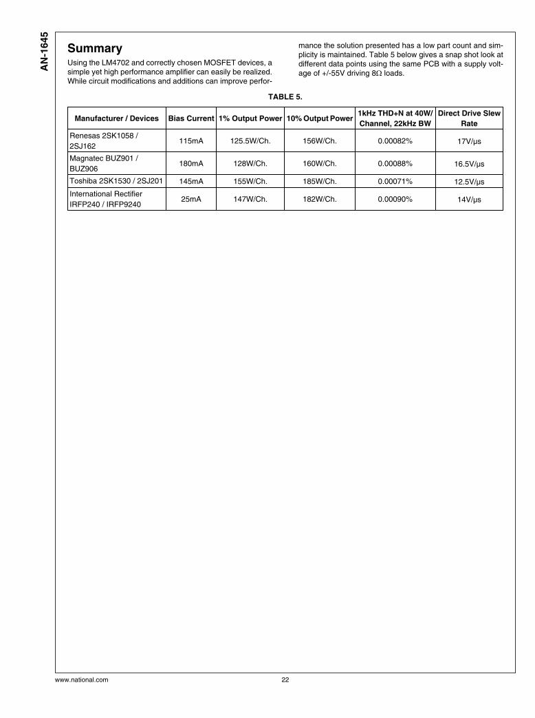
SummaryUsing the LM4702 and correctly chosen MOSFET devices, asimple yet high performance amplifier can easily be realized.While circuit modifications and additions can improve perfor-
mance the solution presented has a low part count and sim-plicity is maintained. Table 5 below gives a snap shot look atdifferent data points using the same PCB with a supply volt-age of +/-55V driving 8Ω loads.
TABLE 5.
Manufacturer / Devices Bias Current 1% Output Power 10% Output Power1kHz THD+N at 40W/
Channel, 22kHz BW
Direct Drive Slew
Rate
Renesas 2SK1058 /
2SJ162115mA 125.5W/Ch. 156W/Ch. 0.00082% 17V/μs
Magnatec BUZ901 /
BUZ906180mA 128W/Ch. 160W/Ch. 0.00088% 16.5V/μs
Toshiba 2SK1530 / 2SJ201 145mA 155W/Ch. 185W/Ch. 0.00071% 12.5V/μs
International Rectifier
IRFP240 / IRFP924025mA 147W/Ch. 182W/Ch. 0.00090% 14V/μs
www.national.com 22
AN
-1645

Revision Table
Rev Date Description
1.0 05/24/07 Initial WEB release.
23 www.national.com
AN
-1645

NotesA
N-1
645
LM
4702 D
rivin
g a
MO
SF
ET
Ou
tpu
t S
tag
e
THE CONTENTS OF THIS DOCUMENT ARE PROVIDED IN CONNECTION WITH NATIONAL SEMICONDUCTOR CORPORATION(“NATIONAL”) PRODUCTS. NATIONAL MAKES NO REPRESENTATIONS OR WARRANTIES WITH RESPECT TO THE ACCURACYOR COMPLETENESS OF THE CONTENTS OF THIS PUBLICATION AND RESERVES THE RIGHT TO MAKE CHANGES TOSPECIFICATIONS AND PRODUCT DESCRIPTIONS AT ANY TIME WITHOUT NOTICE. NO LICENSE, WHETHER EXPRESS,IMPLIED, ARISING BY ESTOPPEL OR OTHERWISE, TO ANY INTELLECTUAL PROPERTY RIGHTS IS GRANTED BY THISDOCUMENT.
TESTING AND OTHER QUALITY CONTROLS ARE USED TO THE EXTENT NATIONAL DEEMS NECESSARY TO SUPPORTNATIONAL’S PRODUCT WARRANTY. EXCEPT WHERE MANDATED BY GOVERNMENT REQUIREMENTS, TESTING OF ALLPARAMETERS OF EACH PRODUCT IS NOT NECESSARILY PERFORMED. NATIONAL ASSUMES NO LIABILITY FORAPPLICATIONS ASSISTANCE OR BUYER PRODUCT DESIGN. BUYERS ARE RESPONSIBLE FOR THEIR PRODUCTS ANDAPPLICATIONS USING NATIONAL COMPONENTS. PRIOR TO USING OR DISTRIBUTING ANY PRODUCTS THAT INCLUDENATIONAL COMPONENTS, BUYERS SHOULD PROVIDE ADEQUATE DESIGN, TESTING AND OPERATING SAFEGUARDS.
EXCEPT AS PROVIDED IN NATIONAL’S TERMS AND CONDITIONS OF SALE FOR SUCH PRODUCTS, NATIONAL ASSUMES NOLIABILITY WHATSOEVER, AND NATIONAL DISCLAIMS ANY EXPRESS OR IMPLIED WARRANTY RELATING TO THE SALEAND/OR USE OF NATIONAL PRODUCTS INCLUDING LIABILITY OR WARRANTIES RELATING TO FITNESS FOR A PARTICULARPURPOSE, MERCHANTABILITY, OR INFRINGEMENT OF ANY PATENT, COPYRIGHT OR OTHER INTELLECTUAL PROPERTYRIGHT.
LIFE SUPPORT POLICY
NATIONAL’S PRODUCTS ARE NOT AUTHORIZED FOR USE AS CRITICAL COMPONENTS IN LIFE SUPPORT DEVICES ORSYSTEMS WITHOUT THE EXPRESS PRIOR WRITTEN APPROVAL OF THE CHIEF EXECUTIVE OFFICER AND GENERALCOUNSEL OF NATIONAL SEMICONDUCTOR CORPORATION. As used herein:
Life support devices or systems are devices which (a) are intended for surgical implant into the body, or (b) support or sustain life andwhose failure to perform when properly used in accordance with instructions for use provided in the labeling can be reasonably expectedto result in a significant injury to the user. A critical component is any component in a life support device or system whose failure to performcan be reasonably expected to cause the failure of the life support device or system or to affect its safety or effectiveness.
National Semiconductor and the National Semiconductor logo are registered trademarks of National Semiconductor Corporation. All otherbrand or product names may be trademarks or registered trademarks of their respective holders.
Copyright© 2007 National Semiconductor Corporation
For the most current product information visit us at www.national.com
National SemiconductorAmericas CustomerSupport CenterEmail:[email protected]: 1-800-272-9959
National Semiconductor EuropeCustomer Support CenterFax: +49 (0) 180-530-85-86Email: [email protected] Tel: +49 (0) 69 9508 6208English Tel: +49 (0) 870 24 0 2171Français Tel: +33 (0) 1 41 91 8790
National Semiconductor AsiaPacific Customer Support CenterEmail: [email protected]
National Semiconductor JapanCustomer Support CenterFax: 81-3-5639-7507Email: [email protected]: 81-3-5639-7560
www.national.com