
Appendix d of Barry b Bray
38
APPENDIX D Answers to Selected Even-Numbered Questions and Problems CHAPTER 1 2. Herman Hollerith 4. Konrad Zuse 6. ENIAC 8. Augusta Ada Byron 10. A machine that stores the instructions of a program in the memory system. 12. 200 million 14. 16M bytes 16. 1993 18. 2000 20. Millions of instructions per second 22. A binary bit stores a 1 or a 0. 24. 1024K 26. 1024 28. System area and transient program area 30. 640K 32. 1M 34. 80386, 80486, Pentium, Pentium Pro, PII, PIII, P4, and Core2 36. The basic I/O system 38. The XT was used with the 8088 and 8086 and beginning with the 80286, the AT became the name of the system. 40. 8-bit and 16-bit 42. The advanced graphics port is designed to support video cards. 44. The serial ATA interface is designed to support disk drive memory. 46. 64K 48. See Figure 1–6. 50. Address, data, and control buses. (c) 32-bit signed number (d) 32-bit floating-point number (e) 64-bit floating- point number 58. (a) 156.625 (b) 18.375 (c) 4087.109375 (d) 83.578125 (e) 58.90625 60. (a) 10111 2 , 27 8 , and 17 16 (b) 1101011 2 , 153 8 , and 6B (c) 10011010110 2 , 2326 8 , and 4D6 16 (d) 1011100 2 , 134 8 , and 5C 16 (e) 10101101 2 , 255 8 , and AD 62. (a) 0010 0011 (b) 1010 1101 0100 (c) 0011 0100 . 1010 1101 (d) 1011 1101 0011 0010 (e) 0010 0011 0100 . 0011
-
Upload
danishahmed -
Category
Documents
-
view
227 -
download
1
description
Intel micro porcessor by barry b bray Appendix D
Transcript of Appendix d of Barry b Bray

APPENDIX D
Answers to Selected Even-NumberedQuestions and Problems
CHAPTER 1
2. Herman Hollerith4. Konrad Zuse6. ENIAC8. Augusta Ada Byron10. A machine that stores the instructions of a program in the memory system.12. 200 million14. 16M bytes16. 199318. 200020. Millions of instructions per second22. A binary bit stores a 1 or a 0.24. 1024K26. 102428. System area and transient program area30. 640K32. 1M34. 80386, 80486, Pentium, Pentium Pro, PII, PIII, P4, and Core236. The basic I/O system38. The XT was used with the 8088 and 8086 and beginning with the 80286, the AT became the name of the system.40. 8-bit and 16-bit42. The advanced graphics port is designed to support video cards.44. The serial ATA interface is designed to support disk drive memory.46. 64K48. See Figure 1–6.50. Address, data, and control buses.
(c) 32-bit signed number (d) 32-bit floating-point number (e) 64-bit floating-point number58. (a) 156.625 (b) 18.375 (c) 4087.109375 (d) 83.578125 (e) 58.90625
60. (a) 101112, 278, and 1716 (b) 11010112, 1538, and 6B (c) 100110101102, 23268, and 4D616 (d) 10111002,1348, and 5C16 (e) 101011012, 2558, and AD62. (a) 0010 0011 (b) 1010 1101 0100(c) 0011 0100 . 1010 1101 (d) 1011 1101 0011 0010 (e) 0010 0011 0100 . 001164. (a) 0111 0111 (b) 1010 0101 (c) 1000 1000 (d) 0111 111166. Byte is an 8-bit binary number, word is a 16-bit binary number, doubleword is a 32-bit binary number.68. Enter is a 0DH and it is used to return the cursor/print head to the left margin of the screen or page of paper.70. LINE1 DB ‘What time is it?’72. (a) 0000 0011 1110 1000 (b) 1111 1111 1000 1000 (c) 0000 0011 0010 0000 (d) 1111 0011 0111 010074. char Fred1 = –3476. Little endian numbers are stored so the least signifi- cant portion is in the lowest numbered memory loca- tion and big endian numbers are stored so the most significant part is stored in the lowest numbered memory location.78. (a) packed = 00000001 00000010 and unpacked

00000001 00000000 00000010 (b) packed =01000100 and unpacked 00000100 00000100 (c) packed = 00000011 00000001 and unpacked00000011 00000000 00000001 (d) packed =00010000 00000000 and unpacked 0000000152.MRDC00000000 00000000 0000000054. Memory read operation56. (a) 8-bit signed number (b) 16-bit signed number80. (a) 89 (b) 9 (c) 32 (d) 182. (a) +3.5 (b) -1.0 (c) +12.5
897
898 APPENDIX D
CHAPTER 2
2. 164. EBX6. Holds the offset address of the next step in the program.8. No, if you add +1 and –1 you have zero, which is a valid number.10. The I-flag.12. The segment register addresses the lowest address in a 64K memory segment.14. (a) 12000H (b) 21000H (c) 24A00H (d) 25000H (e) 3F12DH16. DI18. SS plus either SP or ESP20. (a) 12000H (b) 21002H (c) 26200H (d) A1000H (e) 2CA00H22. All 16M bytes24. The segment register is a selector that selects the descriptor from a descriptor table. It also sets privi- lege level of the request and chooses either the global or local table.26. A00000H–A01000H28. 00280000H–00290FFFH30. 332. 64K
34.
36. Through a descriptor stored in the global table38. The program invisible registers are the cache portions of the segment registers and also the GDTR, LDTR, and IDTR registers.40. 4K42. 102444. Entry zero or the first entry46. The TLB caches the most recent memory accesses through the paging mechanism.50. 1T
CHAPTER 3
2. AL, AH, BL, BH, CL, CH, DL, and DH4. EAX, EBX, ECX, EDX, ESP, EBP, EDI, and ESI6. CS, DS, ES, SS, FS, and GS8. You may not specify mixed register sizes.
0000 0011 1101 0000
1001 0010 0000 0000
0000 0000 0000 0000
0010 1111 1111 1111

10. (a) MOV AL,12H (b) MOV AX,123AH(c) MOV CL,0CDH (d) MOV RAX,1000H (e) MOV EBX,1200A2H12. Selects an assembly language programming model that contains a single segment that compiles as a .COM program.14. A label is a symbolic memory address.16. A label may begin with a letter and some special characters, but not with a number.18. The .TINY model creates a .COM program.20. A displacement is a distance and in MOV DS:[2000H],AL the displacement of 2000H is added to the contents of DS times 10H to form the memory address.22. (a) 3234H (b) 2300H (c) 2400H24. MOV BYTE PTR [2000H],626. MOV DWORD PTR DATA1, 528. The MOV BX,DATA instruction copies the word from memory location data into the BX register where the MOV BX,OFFSET DATA instruction copies the offset address of DATA into BX.30. Nothing is wrong with the instruction; it just uses an alternative addressing style.32. (a) 11750H (b) 11950H (c) 11700H34. BP or as an extended version EBP36. FIELDS STRUCF1 DW ?F2 DW ?F3 DW ?F4 DW ?F5 DW ?FIELDS ENDS
38. Direct, relative, and indirect40. The intersegment jump allows jumps between seg- ments or to anywhere in the memory system while the intrasegment jump allows a jump to any location within the current code segment.42. 3244. Short46. JMP BX48. 250. AX, CX, DX, BX, SP, BP, DI, and SI in the same order as listed52. PUSHFD
CHAPTER 4
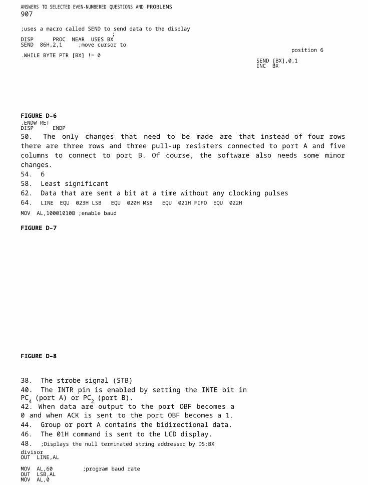
2. The D-bit indicates the direction of flow for the data (REG to R/M or R/M to REG) and the W-bit indicates the size of the data (byte or word/doubleword).4. DL6. DS:[BX+DI]8. MOV AL,[BX]10. 8B 77 0212. The REX prefix, which is used in the 64-bit flat mode, is the register extension that allows the 64-bit registers to be addressed in an instruction.
ANSWERS TO SELECTED EVEN-NUMBERED QUESTIONS AND PROBLEMS 899
14. MOV AX,1000H MOV DS,AX16. PUSH RAX18. AX, CX, DX, BX, SP, BP, SI, and DI20. (a) AX is copied to the stack. (b) A 32-bit number is retrieved from the stack and placed into ESI. (c) The word contents of the data segment memory location addressed by BX is pushed onto the stack. (d) EFLAGS are pushed onto the stack. (e) A word is retrieved from the stack and placed into DS. (f) A 32-bit number 4 is pushed onto the stack.22. Bits 24–31 of EAX are stored in location 020FFH, bits 16–23 of EAX are stored into location 020FEH, bits 8–15 of EAX are stored into location 020FDH, and bits 0–7 of EAX are stored into location 020FCH. SP is then decremented by 4 to a value of 00FCH.24. There are many possible locations, but SP = 0200Hand SS = 0200H is one of them.26. Both instruction load the address of NUMB into DI.The difference is that the MOV DI,OFFSET NUMB assembles as a move immediate and the LEA DI,NUMB assembles as an LEA instruction.28. The LDS BX,NUMB instruction loads BX with the word stored at data segment memory location NUMB and DS is loaded from the data segment memory location addressed by NUMB+2.30. MOV BX,NUMBMOV DX,BX

MOV SI,DX
32. CLD clears the direction flag and STD sets the direc- tion flag.34. The LODSB instruction copies a byte of data from the data segment memory location addressed by SI into the AL register and then increments SI by one if the direction flag is cleared.36. The OUTSB instruction sends the contents of the data segment memory location addressed by SI to the I/O port address by DX, then SI is incremented by one if the direction flag is cleared.38. MOV SI,OFFSET SOURCEMOV DI,OFFSET DESTMOV CX,12REP MOVSB
40. XCHG EBX,ESI42. The LAHF and SAHF instructions in non-64-bit application with the arithmetic coprocessor.44. The XLAT instruction passes the contents of AL to BX to form an offset address that accesses a memory location whose content is then copied into AL.46. The OUT DX,AX instruction copies the 16-bit contents of AX into the data segment memory location addressed by the DX register.48. MOV AH,ES:[BX]50. An assembly language directive is a special command to the assembler that may or may not generate code or data for the memory.52. The directives, DB, DW, and DD, are used to define memory as a byte (DB), a word (DW), and a double- word (DD).54. The EQU (equate) directive allows a memory loca- tion to be equated to another memory location.56. The .MODEL directive specifies the type of memory model used for a program.58. Full segment definitions60. PROC indicates the start of a procedure and ENDPindicates its end.62. STORE PROC NEARMOV [DI],ALMOV [DI+1],ALMOV [DI+2],ALMOV [DI+3],ALRETSTORE ENDP64. COPY PROC FARMOV AX,CS:DATA4MOV BX,AXMOV CX,AXMOV DX,AXMOV SI,AXRETCOPY ENDP
CHAPTER 5
2. You cannot use mixed-size registers.4. AX = 3100H, C = 0, A = 1, S = 0, Z = 0, and O = 0.
6. ADD AX,BXADD AX,CXADD AX,DXADD AX,SP
8. MOV DI,AXMOV R12,RCXADD R12,RDXADD R12,RSI
10. INC SP12. (a) SUB CX,BX (b) SUB DH,0EEH (c) SUB SI,DI (d) SUB EBP,3322H (e) SUB CH,[SI] (f) SUB DX,[SI+10] (g) SUB FROG,AL (h) SUB R10,R914. MOV BX,AXSUB BX,DISUB BX,SISUB BX,BP
16. The contents of DX and the carry flag are subtracted from the 16-bit contents of the data segment memory addressed by DI – 4 and the result is placed into DX.18. AH (most significant) and AL (least significant)20. The O and C flags contain the state of the most sig- nificant portion of the product. If the most significant part of the product is zero, then C and O are zero.22. MOV DL,5MOV AL,DLMUL DLMUL DL
24. BX = DX times 100H

900 APPENDIX D
26. AX28. The errors detected during a division are a divide overflow and a divide by zero.30. AH
32. MOV AH,0MOV AL,BLDIV CLADD AL,ALMOV DL,ALMOV DH,0ADC DH,0
34. It divides by AL by 10. This causes numbers between0 and 99 decimal to be converted to unpacked BCD inAH (quotient) and AL (remainder).36. PUSH DXPUSH CXMOV CX,1000DIV CXMOV [BX],ALMOV AX,DXPOP CXPOP DXPUSH AXAAMMOV [BX+1],AHMOV [BX+2],ALPOP AXMOV AL,AHAAMMOV [BX+3],AHMOV [BX+4],AL
38. Neither the BCD or the ASCII instructions function in the 64-bit mode.40. MOV BH,DH
AND BH,1FH42. MOV SI,DI
OR SI,1FH44. OR AX,0FH
AND AX,1FFFHXOR AX,0380H
46. TEST CH,4segment memory location addressed by DI. The JMP FAR PTR[DI] instruction jumps to the new offset address stored in the data segment memory location addressed by DI and the new segment addressed by the data segment memory location address by DI+2. JMP [DI] is a near jump and JMP FAR PTR [DI] is a far jump.14. JA tests the condition of an arithmetic or logic instruc- tion to determine if the outcome is above. If the outcome is above a jump occurs, otherwise no jump occurs.16. JNE, JE, JG, JGE, JL, or JLE18. JA and JBE20. SETZ or SETE22. ECX24. MOV DI,OFFSET DATAZMOV CX,150HCLDMOV AL,00HL1: STOSBLOOP L126. CMP AL,3JNE @C0001ADD AL,2@C0001:28. MOV SI,OFFSET BLOCKAMOV DI,OFFSET BLOCKBCLD.REPEAT
LODSBSTOSB
.UNTIL AL == 030. MOV AL,0MOV SI,OFFSET BLOCKAMOV DI,OFFSET BLOCKBCLD.WHILE AL != 12H
LODSBADD AL,[DI]MOV [DI],AL
48. (a) SHR DI,3 (b) SHL AL,1 (c) ROL AL,3
.ENDW

INC DI(d) RCR EDX,1 (e) SAR DH,150. Extra52. The SCASB instruction is repeated while the condi- tion is equal as long as CX is not zero.54. CMPSB compares the byte contents of the byte in the data segment addressed by SI with the byte in the extra segment addressed by DI.56. In DOS the letter C is displayed.
CHAPTER 6
2. A near JMP instruction4. A far jump6. (a) near (b) short (c) far8. The IP or EIP register10. The JMP AX instruction jumps to the offset address stored in AX. This can only be a near jump.12. The JMP [DI] instruction jumps to the memory location addressed by the offset address stored in the data32. A procedure is a reusable group of instructions that ends with a RET.34. RET36. By using NEAR or FAR to the right of the PROCdirective
38. CUBE PROC NEAR USES AX DXMOV AX,CXMUL CXMUL CXRETCUBE ENDP40. SUMS PROC NEARMOV EDI,0ADD EAX,EBXADD EAX,ECXADD EAX,EDXADC EDI,0RETSUMS ENDP
42. An interrupt is a hardware-initiated function call.44. INT 0 through INT 25546. The interrupt vector is used to detect and respond to divide errors.
ANSWERS TO SELECTED EVEN-NUMBERED QUESTIONS AND PROBLEMS 901
48. The IRETD instruction is a 32-bit return that pops the return address into EIP.50. When overflow is a 152. CLI and STI54. If the value in the register or memory location under test in the destination operand is below or above the boundaries stored in the memory address by the source operand.56. BP
CHAPTER 7
2. No, bytes must be defined in C++ using char.4. EAX, EBX, ECX, EDX, and ES6. Floating-point coprocessor stack8. Data are accessed in array string using register SI to index the string element.10. If no headers are used for a C++ program, it will be much smaller.12. No. INT 21H is a 16-bit DOS call that cannot be used in the Windows 32-bit environment.14. #include “stdafx.h”#include <conio.h>
int _tmain(int argc, _TCHAR* argv[]){
.code ;start code segment
public RotateLeft3 ;define RotateLeft3 as a public function
RotateLeft3 proc ;define procedureRotatedata:byte ;define byte
mov al,Rotatedata rol al,3ret
RotateLeft3 endp

32. ;Function that converts;.model flat,c.stack 1024.code
Public Upper
Upper procChar:byte
mov al,Char.if al >= 'a' && a; <= 'z'
sub al,30h.endifRetUpper endp
34. Properties contains information about an object such as the foreground and background colors, etc.36. _asm inc ptr;
char a = 0;while ( a != ?@?){
a = _getche();_putch(a);
}return 0;}
16. The _putch(10) instruction displays the new line function and the _putch(13) returns the cursor to the left margin of the display.18. Separate assembly modules are the most flexible.20. The flat model must be used with the C prototype as in .MODEL FLAT,C and the function that is linked to C++ must be made public.22. A 16-bit word is defined with the short directive.
24. Examples of events are mouse move, key down, etc.Event handlers catch these events so they can be used in a program.26. Yes. The C++ editor can be used to edit an assembly language module, but the module must use the .TXT extension instead of .ASM.
28. #define RDTSC _asm _emit 0x0f _asm _emit 0x3130. ;;External function rotates a byte 3 placesleft;.586 ;select Pentium and 32-bit model.model flat, C ;select flat model withC/C++ linkage.stack 1024 ;allocate stack space
CHAPTER 8
2. The TEST.ASM file, when assembled, generates the TEST.OBJ file and the TEST.EXE file if no switches appear on the command line.4. PUBLIC indicates that a label is available to other program modules.6. EXTRN8. MACRO and ENDM10. Parameters are passed to a macro through a parameter list that follows the MACRO keyword (on the same line).12. The LOCAL directive defines local labels and must be on the line immediately following the MACRO line.14. ADDM MACRO LIST,LENGTH PUSH CXPUSH SIMOV CX,LENGTHMOV SI,LISTMOV AX,0.REPEATADD AX,[SI]INC SI.UNTILCXZPOP SIPOP CXENDM
16. private: System::Void textBox1_KeyDown (System::Objectˆ sender,System:: Windows::Forms::KeyEventArgsˆ e)
902 APPENDIX D
{// this is called firstkeyHandled = true;if (e->KeyCode >= Keys::D0 &&

e->KeyCode <= Keys::D9 &&e->Shift == false){keyHandled = false;}}
18. private: System::Void textBox1_KeyDown (System::Objectˆ sender,System::Windows:: Forms::KeyEventArgsˆ e)
if ( direction )_asm rol temp1,1;
else_asm ror temp1,1;data1 = temp1;for (int a = 128; a > 0; a>>=1){if ( ( temp1 & a ) == a )temp += “1”;
elsetemp += “0”;}label2->Text = temp;}{{
RandomNumber++; //a global variableif ( RandomNumber == 63 )
RandomNumber = 9;}}
20. bool direction;private: System::Void button1_Click(System::Objectˆ sender,System::EventArgsˆ e){label1->Text = “Shift Left = ”;shift = true;data1 = 1;label2->Text = “00000001”;timer1->Start();}
private: System::Void button1_Click(System:: Objectˆ sender,System::EventArgsˆ e){label1->Text = “Rotate Left = ”;shift = false;data1 = 1;label2->Text = “00000001”;timer1->Start();}
private: System::Void radiobutton1_Click(System::Objectˆ sender,System::EventArgsˆ e){// left buttondirection = true; //new bool variableif ( shift )label1->Text = “Shift Left = ”;elselabel1->Text = “Rotate Left = ”;}
private: System::Void radiobutton2_Click(System::Objectˆ sender,System::EventArgsˆ e){// left buttondirection = false; //new bool variableif ( shift )label1->Text = “Shift Right = ”;elselabel1->Text = “Rotate Left = ”;22. The MouseEventArgs in MouseDown contains theButton state that is tested against ::mouses::Mouse Buttons::Right to intercept the right mouse button in a program.24. private: System::Void Form1_MouseDown (System::Objectˆ sender,System::Windows:: Forms::MouseEventArgsˆ e){if (e->Button ==::mouses::MouseButtons::Left &&e->Button == ::mouses::MouseButtons::Right){
//left and right}}
26. ForeColor sets the color of the text or characters in a control.28. A large number is converted by repeated divisions by the number 10. After each digit the remainder is saved as a significant digit of the BCD result.

30. 30H32. int GetOct(void)
{Stringˆ temp;int result = 0;char temp1;temp = textBox1-≥Text;for ( int a = 0; a < temp->Length; a++ ){temp1 = temp.[a];_asm
{shl result,3mov eax,0mov al,temp1sub al,30hor result,eax
}}return result;}}
private: System::Void timer1_Tick(System:: Objectˆ sender,System::EventArgsˆ e){Stringˆ temp = “”;char temp1 = data1;if ( shift )if ( direction )_asm shl temp1,1;
else_asm shr temp1,1;else
34. char Up(char temp){if ( temp >= 'a' && temp <= 'z' )_asm sub temp,20h;Return temp;}
36. The boot sector is where a bootstrap loader program is located that loads the operating system. The FAT is a table that contains numbers that indicate whether a cluster is free, bad, or occupied. If occupied, an

ANSWERS TO SELECTED EVEN-NUMBERED QUESTIONS AND PROBLEMS 903
FFFFH indicates the end of a file chain or the next cluster number in the file chain. The director holds information about a file or a folder.38. Sectors.40. A cluster is a grouping of sectors.42. 4G bytes44. 846. 256return numb;}
//code placed in the OnInitDlg function int tempval = 1;for ( int a = 0; a < 8; a++ ){CString temp = "2^ = ";temp.SetAt(2, a + 0x30);temp += GetNumb(tempval);List.InsertString(a, temp);tempval <<= 1;
48. File::Replace(?TEST.LST?, ?TEST.LIS?, ?TEST.BAK?);// Creates TEST.LIS and TEST.BAK, DeletesTEXT.LST
50. A control is a common object that can be used in any visual programming language.52. See Figure D–1 for the output (the stock ListBox con- tains the output).
String CPowersDlg::GetNumb(int temp){char numb[10];_asm{
mov eax,tempmov ebx,10push ebxmov ecx,0
loop1:mov edx,0div ebxpush edxcmp eax,0jnz loop1
loop2:pop edxcmp edx,ebxje loop3add dl,30h
mov numb[ecx],dlinc ecxjmp loop2
loop3:mov byte ptr numb[ecx],0}
FIGURE D–1}
54. private: System::Void Clear(){

panel1->Visible = false;panel2->Visible = false;panel3->Visible = false;panel4->Visible = false;panel5->Visible = false;panel6->Visible = false;panel7->Visible = false;}
private: System::Void Form1_KeyDown(System:: Objectˆ sender,System::Windows::Forms:: KeyEventArgsˆ e){char lookup[] = {0x3f, 6, 0x5b, 0x4f,
0x66, 0x6d, 0x7d, 7, 0x7f,0x6f,0x77, 0x7c, 0x39, 0x5e, 0x79,0x71};
if (e->KeyCode >= Keys::D0 &&e->KeyCode <= Keys::D9)
{ShowDigit(lookup
[e->KeyValue -0x30]); //display
the digit}else if (e->KeyCode >= Keys::A &&
e->KeyCode <= Keys::F){ShowDigit(lookup
[e->KeyValue -0x37]); //display
letter)}
private: System::Void ShowDigit(unsigned char code){Clear();if (( code & 1 ) == 1) //test a
segmentpanel1->Visible = true;if (( code & 2 ) == 2) //test b
segmentpanel4->Visible = true;if (( code & 4 ) == 4) //test c
segmentpanel5->Visible = true;if (( code & 8 ) == 8) //test d
segmentpanel3->Visible = true;if (( code & 16 ) == 16) //test e
segmentpanel6->Visible = true;if (( code & 32 ) == 32) //test f
segmentpanel7->Visible = true;if (( code & 64 ) == 64) //test g
segmentpanel2->Visible = true;}

904 APPENDIX D
private: System::Void Form1_Load(System:: Objectˆ sender,System::EventArgsˆ e){
Clear();}
CHAPTER 9
2. Yes and no. The current drive of a logic zero is reduced to 2.0 mA and the noise immunity is reduced to 350 mV.4. Address bits A0–A7
6. A read operation8. The duty cycle must be 33%.10. A write is occurring.12. The data bus is sending data to the memory or I/O.14. IO/M, DT/R, and SS016. Signals to the coprocessor, which indicate what the microprocessor queue is doing.18. 320. 14 MHz/6 = 2.33 MHz22. Address bus connection A0–A1524. 74LS373 transparent latch26. If too many memory and/or I/O devices are attached to a system the buses must be buffered.28. 430. Fetch and execute32. (a) The address is output along with ALE (b) Time is allowed for memory access and the READY input is sampled. (c) The read or write signal is issued. (d) Data are transferred and read or write isdeactivated. (e) Wait allows additional time for memory access.36. Selects one or two stages of synchronization forREADY38. Minimum mode operation is most often used in embedded applications and maximum mode opera- tion was most often used in early personal computers.
CHAPTER 10
2. (a) 256 (b) 2K (c) 4K (d) 8K (e) 1M4. Select the memory device6. Cause a write to occur8. The microprocessor allows 460 ns for memory at5 MHz, but because there is a small delay in the con- nections to the memory, it would be best not to use a450 ns memory device in such a system without one wait state.10. Static random access memory12. 250 ns14. The address inputs to many DRAMs are multiplexed so one address input accepts two different address bits, reducing the number of pins required to address memory in a DRAM.16. Generally the amount of time is equal to a read cycle and represents only a small amount of time in a mod- ern memory system.18. See Figure D–2.20. One of the eight outputs becomes a logic zero as dic- tated by the address inputs.
A17
U1A
1 2
A19A18A16A15A14

A13A12A11
74ALS04
U1B
1 U2
234567 9101112131415
74ALS133
3 4IO/M
74ALS04
FIGURE D–2
ANSWERS TO SELECTED EVEN-NUMBERED QUESTIONS AND PROBLEMS 905
A17
A16
A13A14A15
A18A19
U1A 1
2
74ALS32
A Y0B Y1C Y2
Y3
G1 Y4Y5
G2A Y6G2B Y7
2 143 13
6
121110
4 95 7
74ALS138

U21 15
40000H–41FFFH42000H–43FFFH44000H–45FFFH46000H–47FFFH48000H–49FFFH4A000H–4BFFFH4C000H–4DFFFH4E000H–4FFFFH
FIGURE D–3
48. Yes, as long as a memory location on the DRAM is not accessed.50. 128 bits wide
FIGURE D–4
22. See Figure D–3.24. Verilog hardware description language26. The architecture block between begin and endCHAPTER 11
2. The I/O address is stored in the second byte of the instruction.4. DX6. The OUTSB instruction transfers the data segment byte addressed by SI to the I/O port addressed by DX, then SI is incremented by one.8. Memory mapped I/O uses any instruction that transfers data to or from the memory for I/O, while isolated I/O
28.MRDC and MWTCrequires the use of the IN or OUT instruction.
30. See Figure D–4.32. 534. 110. The basic output interface is a latch that captures out-put data and holds it for the output device.12. Lower
36.
BHE selects the upper memory bank and A0 selects the lower memory bank.14. 416. It removes mechanical bounces from a switch.38. Separate decoders and separate write signals40. Lower memory bank42. library ieee;use ieee.std_logic_1164.all;entity DECODER_10_28 isport (A23, A22, A21, A20, A19, A18, A17,A16, A0, BHE, MWTC: in STD_LOGIC;SEL, LWR, HWR: out STD_LOGIC);
end;
architecture V1 of DECODER_10_28 is begin
SEL <= A23 or A22 or A21 or A20 or A19 or A18 or (not A17) or (not A16);LWR <= A0 or MWTC; HWR <= BHE or MWTC;
end V1;
44. See Figure D–5.18. See Figure D–6.20. See Figure D–7.22. See Figure D–8.

24. If the port is 16 bits wide, there is no need to enable either the low or high half.26. D47–D4028. Group A is port A and PC4–PC7, while group B isport B and PC3–PC0.30. RD32. Inputs34. The strobe input latches the input data and sets the buffer full flag and interrupt request.36. DELAY PROC NEAR USES ECX
MOV ECX, 7272727D1:LOOPD D1RET
DELAY ENDP

FIGURE D–5
906

ANSWERS TO SELECTED EVEN-NUMBERED QUESTIONS AND PROBLEMS 907
;uses a macro called SEND to send data to the display;
DISP PROC NEAR USES BXSEND 86H,2,1 ;move cursor to
position 6.WHILE BYTE PTR [BX] != 0
SEND [BX],0,1INC BX
FIGURE D–6.ENDW RETDISP ENDP
50. The only changes that need to be made are that instead of four rows there are three rows and three pull-up resisters connected to port A and five columns to connect to port B. Of course, the software also needs some minor changes.54. 658. Least significant62. Data that are sent a bit at a time without any clocking pulses64. LINE EQU 023H LSB EQU 020H MSB EQU 021H FIFO EQU 022H
MOV AL,10001010B ;enable baud
FIGURE D–7
FIGURE D–8
38. The strobe signal (STB)40. The INTR pin is enabled by setting the INTE bit inPC4 (port A) or PC2 (port B).42. When data are output to the port OBF becomes a0 and when ACK is sent to the port OBF becomes a 1.44. Group or port A contains the bidirectional data.46. The 01H command is sent to the LCD display.48. ;Displays the null terminated string addressed by DS:BXdivisorOUT LINE,AL
MOV AL,60 ;program baud rateOUT LSB,ALMOV AL,0OUT MSB,AL
MOV AL,00011001B ;program 7-data, oddOUT LINE,AL ;parity, one stop
MOV AL,00000111B ;enable transmitter andOUT FIFO,AL ;and receiver

66. Simplex = receiving or sending data; half-duplex = receiving and sending data; but only one direction at a time; and full-duplex = receiving and sending data at the same time.68. SENDS PROC NEAR
MOV CX,16.REPEAT
.REPEATIN AL,LSTAT ;get linestatus registerTEST AL,20H ;test TH bit.UNTIL !ZERO?LODSB ;get dataOUT DATA,AL ;transmit data.UNTILCXZ
RET SENDS ENDP
70. 0.01V72. .MODEL TINY.CODE.STARTUP
MOV DX,400H.WHILE 1
908 APPENDIX D
MOV CX,256MOV AL,0.REPEAT
OUT DX,ALINC AL
CALL DELAY.UNTILCXZMOV CX,256.REPEAT
OUT DX,ALDEC AL
CALL DELAY.UNTILCXZ.ENDW
DELAY PROC NEAR
; 39 microsecond time delay
DELAY ENDP END
74. INTR indicates that the converter has completed a conversion.76. See Figure D–9.
CHAPTER 12
2. An interrupt is a hardware- or software-initiated sub- routine call.4. Interrupts only use computer time when the interrupt is activated.
6. INT, INT3, INTO, CLI, and STI8. The first 1K byte of the memory system in real mode and anywhere in protected mode.10. 00H through 1FH12. Anywhere in the memory system14. A real mode interrupt pushes CS, IP, and the FLAGS onto the stack, while a protected mode interrupt pushes CS, EIP, and the EFLAGS onto the stack.16. The INTO occurs if overflow is set.18. The IRET instruction pops the flags and the return address from the stack.20. The state of the interrupt structure is stored on the stack, so when the return occurs, it is restored. Both the interrupt and trace flags are cleared.22. The IF flag controls whether the INTR pin is enabled or disabled.24. The IF flag is enabled or disabled by using the STI orCLI instructions.26. 228. Level sensitive30. Vector32. See Figure D–10.34. The pull-up resistors guarantee that vector number fetched from the data bus during an interrupt acknowledge is an FFH.36. Because the interrupt request signal (INTR) is gener- ated by ORing all the requests together, the software must ask or poll each device to determine which device caused the request.
38. 940. The CAS pins are cascade pins used to cascade 8259s for more than eight interrupt inputs.42. An OCW is an operational control word for the 8259.44. ICW2
D0–D7
A7 2 I2A8 3 I3A9 4 I4
O2 18
O3 17
O4 16
U3
DB0DB1DB2DB3DB4DB5DB6
1 CS2 RD
VI+ 6
VI– 7
CLKR 19
CLK< 4
VREF 9
A105 I5O5 15 MRDC3
WRA11A12
6 I67 I7O6 14
O7 13
MWTC5 INTR
AGND 8
A13A14A15
8 I8 O8 129 I911 I10
16L8 1
ADC0804
3 2D0
U2A74LS125
A1 18A2 17A3 16A4 15A5 14A6 13
U1 12

FIGURE D–9
ANSWERS TO SELECTED EVEN-NUMBERED QUESTIONS AND PROBLEMS 909
INTA
VCC
1K
2468
11131517
119
U1
1A11A21A31A42A12A22A32A4
1G2G
74ALS244
1Y1 18 D71T2 16 D61Y3 14 D51Y4 12 D42Y1 9 D32Y2 7 D22Y3 5 D12Y4 3 D0
mechanism is silent and very accurate because its placement can be continuously adjusted.28. A CD-ROM is an optical device for storing music or digital data and has a capacity of about 660M or700M (80 minute) bytes.30. A TTL monitor uses TTL signals to generate a dis- play and an analog monitor uses analog signals.32. Cyan, magenta, and yellow34. 1024 lines with 1280 horizontal elements per line36. The DVI-D and HDMI connectors are the latest style of digital video input connectors for all types of video equipment.38. 16 million colors
FIGURE D–10
46. Program sensitivity and single or multiple 8259s48. The most recent interrupt request level becomes the lowest level interrupt after being serviced.

50. INT 8 through INT 0FH
CHAPTER 13
2. When a 1 is placed on HOLD, the program stops exe- cuting and the address, data, and control buses go to their high-impedance state.4. I/O to memory6. DACK8. The microprocessor is in its hold state and the DMAcontroller has control of the buses.10. 412. The command register16. A pen drive is a USB device that acts as a storage device using a flash memory.18. Tracks20. Cylinder22. See Figure D–11.24. The heads in a hard disk drive are aerodynamically designed to ride on a cushion of air as the disk spins and are therefore called flying heads.26. The stepper motor positioning mechanism is noisy and not very precise, while the voice coil positioning
CHAPTER 14
2. Word (16-bits, ±32K), doubleword (32-bits, ±2G), and quadword (64-bits, ±9 × 10¹⁸)4. Single-precision (32 bits), double-precision (64 bits), and temporary-precision (80 bits)6. (a) -7.75 (b) .5625 (c) 76.5 (d) 2.0 (e) 10.0 (f) 0.08. The microprocessor continues executing micro- processor (integer) instructions while the coprocessor executes a floating-point instructions.10. It copies the coprocessor status register to AX.12. By comparing the two registers and then by transfer- ring the status word to the AX register. If the SAHF instruction is next executed, a JZ instruction can be used to test the outcome of the coprocessor compare instruction.14. FSTSW AX16. Data are always stored as an 80-bit temporary preci- sion number.18. 020. Affine allows positive and negative infinity, while projective assumes infinity is unsigned.22. Extended (temporary) precision24. The contents of the top of the stack are copied into memory location DATA as a floating-point number.26. FADD ST,ST(3)28. FSUB ST(2),ST
1 0 0 1 0 1 0 0 0 0
D C D D C C C
FIGURE D–11
910 APPENDIX D
30. Forward division divides the top of the stack by the contents of a memory location and returns the quo- tient to the top of the stack. Reverse division divides the top of the stack into the contents of the memory
POWFLD TEMP FYL2XFSTP TEMPMOV ECX,TEMPRETENDPlocation and returns the result to the top of the stack.

If no operand exists, then forward division divides ST(1) by ST and reverse division divides ST by ST(1).32. It performs a MOV to ST if the condition is below.34. RECIP PROC NEAR MOV TEMP,EAX FLD TEMPFLD1FDIVRFSTP TEMPMOV EAX,TEMPRECIP ENDPTEMP DD ?
36. Finds the function 2X – 1.38. FLDPI40. It indicates that register ST(2) is free.
42. The state of the machine44. CAPR PROC NEAR FLDPIFADD ST,ST(1)FMUL FFMUL C1FLD1FDIVRFTSP XCRETCAPR ENDP
46. In modern software it is never used.48. TOT PROC NEAR FLD R2FLD1FDIVRFLD R3FLD1FDIVRFLD R4FLD1FDIVRFADDFADDFLD1FDIVFADD R1FSTP RTRETTOT ENDP
50. PROD PROC NEAR MOV ECX,100.REPEATFLD ARRAY1[ECX*8–8]FUML ARRAY2[ECX*8–8]FSTP ARRAY3[ECX+8–8].UNTILCXZRETPROD ENDP
52. POW PROC NEAR MOV TEMP,EBX FLD TEMP F2XM1FLD1FADDMOV TEMP,EAX
54. GAIN PROC NEAR MOV ECX,100.REPEATFLD DWORD PTR VOUT[ECX*4–4]FDIV DWORD PTR VIN[ECX*4-4]
CALL LOG10FIMUL TWENTY
FSTP DWORD PTR DBG[ECX*4-4].UNTILCXZRETTWENTY DW 20
GAIN ENDP
56. The EMMS instruction clears the coprocessor stack to indicate that the MMX unit has completed using the stack.58. Signed saturation occurs when byte-sized numbers are added and have values of 7FH for an overflow and80H for an underflow.60. The FSAVE instruction stores all the MMX registers in memory.62. Single-instruction, multiple-data instructions64. 128 bits66. 1668. Yes
CHAPTER 15
2. 8- or 16-bit depending on the socket configuration.4. See Figure D–12.6. See Figure D–13.

8. See Figure D–14.12. 16 bits14. The configuration memory identifies the vendor and also information about the interrupts.16. This is the command/bus enable signal that is high to indicate the PCI bus contains a command and low for data.18. MOV AX,0B108H MOV BX,0MOV DI,8INT 1AH
20. 2.5 GHz22. Yes24. COM130. 1.5 Mbps, 12 Mbps, and 480 Mbps32. 5 meters34. 12736. An extra bit that is thrown in the data stream if more than six ones are sent in a row.38. 1 to 1023 bytes40. The PCI transfers data at 33 MBs, while AGP trans- fers data at 2 GBps (8 ×).

ANSWERS TO SELECTED EVEN-NUMBERED QUESTIONS AND PROBLEMS 911
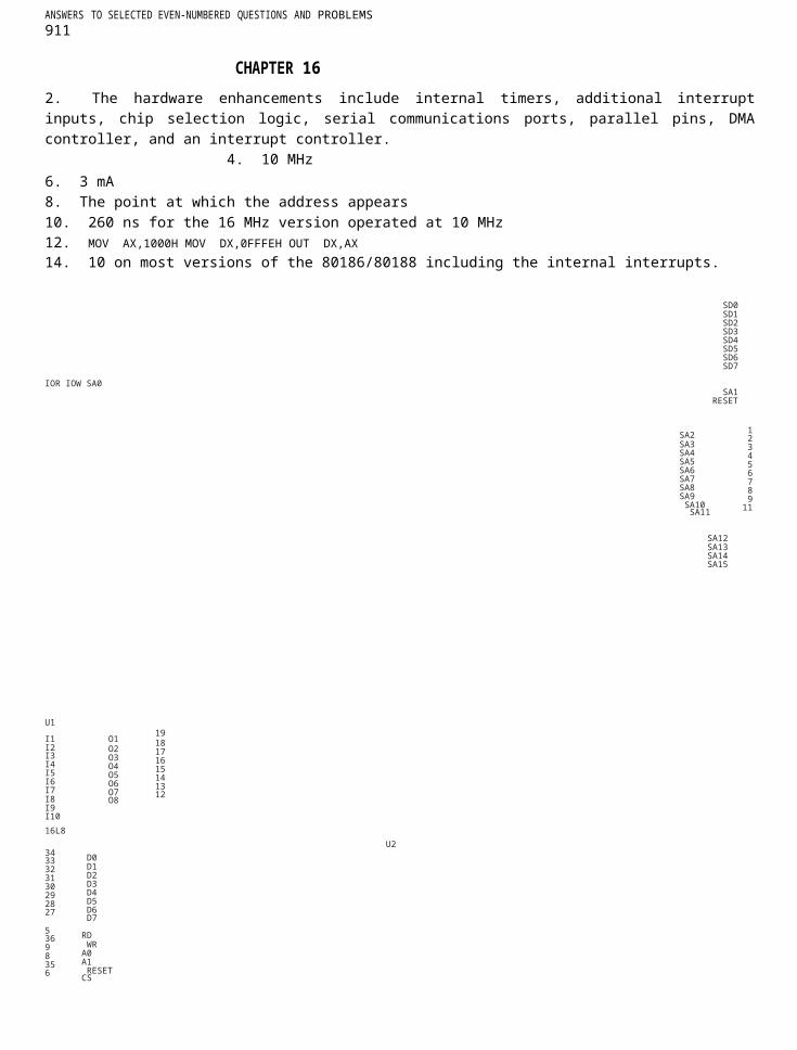
CHAPTER 16
2. The hardware enhancements include internal timers, additional interrupt inputs, chip selection logic, serial communications ports, parallel pins, DMA controller, and an interrupt controller.
4. 10 MHz6. 3 mA8. The point at which the address appears10. 260 ns for the 16 MHz version operated at 10 MHz12. MOV AX,1000H MOV DX,0FFFEH OUT DX,AX14. 10 on most versions of the 80186/80188 including the internal interrupts.
SD0SD1SD2SD3SD4SD5SD6SD7
IOR IOW SA0SA1
RESET
SA2 1
SA3 2
SA4 3
SA5 4
SA6 5
SA7 6
SA8 7
SA9 8
SA10 9
SA11 11
SA12SA13SA14SA15
U1
I1 O1 19
I2 O2 18
I3 O3 17
I4 O4 16
I5 O5 15
I6 O6 14
I7 O7 13
I8 O8 12
I9I10
16L8
U234 D033
D132 D231 D330 D429 D528 D627 D7
5 RD36 WR9
A08 A135
RESET6 CS
82C55
PA0 4

PA1 3PA2 2PA3 1PA4 40PA5 39PA6 38PA7 37
PB0 18
PB1 19PB2 20PB3 21PB4 22PB5 23PB6 24PB7 25
PC0 14
PC1 15PC2 16PC3 17PC4 13PC5 12PC6 11PC7 10
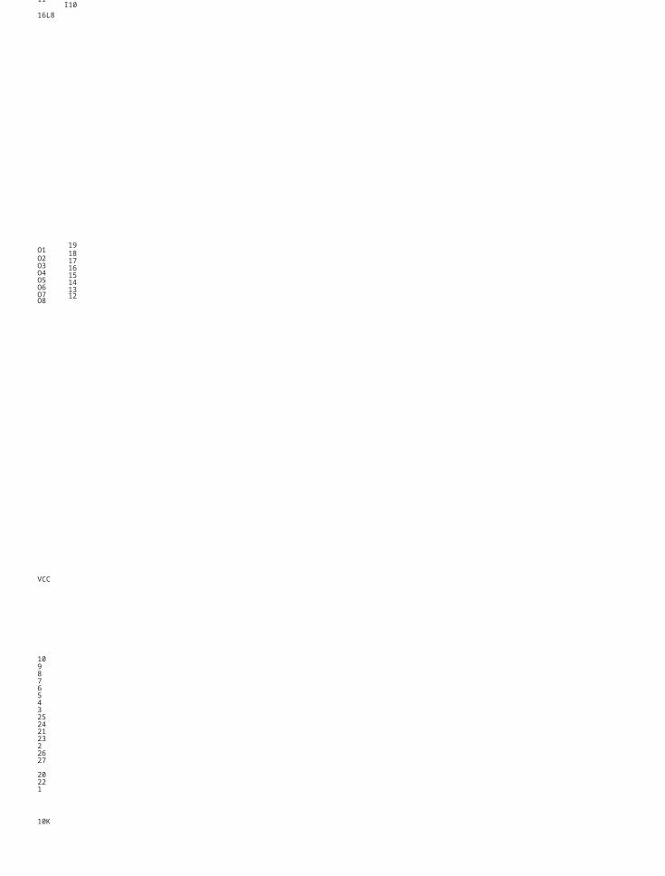
FIGURE D–12
SD7SD6SD5SD4SD3SD2SD1SD0
SA0SA1SA2SA3SA4SA5SA6SA7SA8SA9SA10SA11SA12SA13SA14
SMEMR
SA15SA16SA17SA18SA19LA20LA21LA22LA23
1 I12 I23 I34 I45 I56 I67 I78 I89 I911 I10
16L8

O1 19
O2 18
O3 17
O4 16
O5 15
O6 14
O7 13
O8 12
VCC
1098765432524212322627
20221
10K
U2
A0A1A2A3A4A5
A6A7A8A9A10A11A12A13A14
CE OE VPP
O0 11O1 12O2 13O3 15O4 16O5 17O6 18O7 19
FIGURE D–13

912 APPENDIX D
SD0SD1SD2SD3SD4SD5SD6SD7
U12 1A14 1A26 1A38 1A4
11 2A113 2A215 2A317 2A4
1 1G19 2G
74ALS244
1Y1 181Y2 161Y3 141Y4 122Y1 92Y2 72Y3 52Y4 3
U51
CS2 WR1
18 WR2
7 DI06 DI15 DI24 DI316 DI415 DI514 DI613 DI7
17 XFER19 ILE
10 DGND DAC0830
VREF 8
RFB 9
IOUT2 12
IOUT1 11
AGND 3
4 1 5 U9
– 6
3 +
7417
Channel 800H
SA0SA1SA2SA3SA4SA5SA6SA7SA8SA9
SA10SA11
SA12SA13
2
SA14SA15
U21
I12 I23 I34 I45 I56 I67 I78 I89 I911 I10
16L8
12
45
1918
O2 17O3 16
O4 15O5 14O6 13O7 12O8
U3A
6
U61
CS2 WR1
18 WR2
7 DI06 DI15 DI24 DI316 DI415 DI514 DI613 DI7
17 XFER19 ILE
10 DGND DAC0830
U71 CS2 WR1
VREF 8
RFB 9
IOUT2 12
IOUT1 11
AGND 3
VREF 8
4 1 5 U10
26
3 +
7417
Channel 810H
VCC
O
–

10K74ALS2018 WR2
7 DI06 DI15 DI24 DI316 DI415 DI514 DI6
RFB 9
IOUT2 12
IOUT1 11
4 1 5 U11
2 – 6
3 +
Channel 820H
IOW
9 U3B
8
74ALS2013 DI7
17 XFER19 ILE
10 DGND DAC0830
AGND 3
7417
U81
CS2 WR1
18 WR2
7 DI06 DI15 DI24 DI316 DI415 DI514 DI613 DI7
17 XFER19 ILE
10 DGND DAC0830
VREF 8
RFB 9
IOUT2 12
IOUT1 11
AGND 3
4 1 5 U12
2 – 6
3 +
7417
Channel 830H
10
1213

FIGURE D–14
16. The interrupt control registers control a single interrupt.18. The interrupt poll register acknowledges the inter- rupt, while the interrupt poll status register does not acknowledge the interrupt.20. 322. Timer 224. It determines whether the enable counter bit functions.26. The ALT bit selects both compare registers so the duration of the logic 1 and logic 0 output times can be programmed.28. MOV AX,123MOV DX,0FF5AHOUT DX,AXMOV AX,23ADD DX,2OUT DX,AXMOV AX,0C007HMOV DX,0FF58HOUT DX,AX
30. 232. Place a logic 1 in both the CHG/ NOCHG START/STOP bits of the control register.34. 7
and
ANSWERS TO SELECTED EVEN-NUMBERED QUESTIONS AND PROBLEMS 913
36. Chip38. 1540. It determines the operation of the PCS5 and PCS6 pins.42. MOV AX,1001H MOV DX,0FF90H OUT DX,AX
MOV AX,1048HOUT DX,AX
44. 1G46. Verify for read access.48. An RTOS is a real-time operating system that has a predictable and guaranteed time for threads access.
CHAPTER 17
2. 64T4. See Figure D–15.
6. The memory system has up to 4G bytes and the bank enable signals select one or more of the 8-bit-wide banks of memory.8. The pipeline allows the microprocessor to send the address of the next memory location, while it fetches the data from the prior memory operation. This allows the memory additional time to access the data.10. 0000H–FFFFH12. I/O has the same address as earlier models of the microprocessor. The difference is that the I/O is arranged as a 32-bit-wide space with four 8-bit banks that are selected by the bank enable signals.14. The BS16 pin causes the microprocessor to function with an 8-bit-wide data bus.

16. The first four debug registers (DR0–DR3) contain breakpoint addresses; registers DR4 and DR5 are reserved for Intel’s use; DR6 and DR7 are used to
18. The test registers are used to test the translation look- aside buffer.20. The PE bit switches the microprocessor into protected mode if set and real mode if cleared.22. Scaled-index addressing used a scaling factor of 1, 2,4, or 8 times to scale addressing from byte, word, doubleword, or quadword.24. (a) the address in the data segment at the location pointed to by EBX times 8 plus ECX (b) the address in the data segment array DATA pointed to by the sum of EAX plus EBX (c) the address at data segment location DATA (d) the address in the data segment pointed to by EBX26. Type 13 (0DH)28. The interrupt descriptor table and its interrupt descriptors30. A selector appears in a segment register and it selects a descriptor from a descriptor table. It also contains the requested privilege level of the request.32. The global descriptor table register34. Because a descriptor addresses up to 4G of memory and there are 8K local and 8K global descriptor avail- able at a time, 4G times 16K = 64T.36. The TSS holds linkages and registers of a task so tasks can be switched efficiently.38. The switch occurs when a logic 1 is placed into thePE bit of CR0.40. Virtual mode, which simulates DOS in protectedmode, sets up 1M memory spans that can operate in the real mode.42. 4K44. The 80486 has an internal 8K cache and also contains a coprocessor.46. The register sets are virtually identical.control debugging.48.PCHK and DP0–DP3
FIGURE D–1550. 8K52. A burst is when four 32-bit numbers are read or writ- ten between the cache and memory.54. Built-in self test
CHAPTER 18
FFFFFFFF
Protected Mode
Memory Map
000FFFFF
00000000
Real ModeMemory Map
00000000

2. 64G bytes4. These pins generate and check parity.6. The burst ready pin is used to insert wait state into the bus cycle.8. 18.5 ns10. T212. An 8K byte data cache and an 8K-byte instruction
cache.14. Yes, if one is a coprocessor instruction and the integer instructions are not dependent.
914 APPENDIX D
16. The SSM mode is used for power management in most systems.18. 38000H20. The CMPXCH8B instruction compares the 64-bit number in EDX:EAX with a 64-bit number stored in memory. If they are equal, ECX:EBX is stored in memory. If not equal, the contents of memory are moved into EDX:EAX.22. ID, VIP, VIF, and AC24. To access 4M pages, the page tables are dropped and only the page directory is used with a 22-bit offset address.26. The Pentium Pro is an improved version of the Pentium that contains three integer units, an MMX unit, and a 36-bit address bus.
28. 36 address bits on A3 through A35 (A0–A2 are encoded in the bank selection signals)30. The access time in a 66 MHz Pentium is 18.5 ns and in the Pentium Pro at 66 MHz access time is 17 ns.32. SDRAM that is 72 bits wide is purchased for ECC memory applications instead of 64-bit-wide memory.10. The read and write signals are developed by the chip set instead of the microprocessor.12. 8 ns after the first quadword is accessed. The first quadword still requires 60 ns for access.14. Model-specific registers have been added for SYSENTER_CS, STSENTER_SS, and SYSENTER_ ESP.16. The ECX register address the MSR number when the RDMSR instruction executes. After execution, EDX:EAX contains the contents of the register18. TESTS PROC NEAR CPUIDBT EDX,800HRETTESTS ENDP
20. EDX to the EIP register and the value in ECX to theESP register.22. Ring 324. Pentium Pro26. The Pentium 4 or Core2 requires a power supply with an additional 12 V connector for the main board. A Pentium 4–compliant supply must be used.28. bool Hyper(){
CHAPTER 19
2. 512K, 1M, or 2M4. The Pentium Pro cache is on the main board and the Pentium 2 cache is in the cartridge and operates at a high speed.6. 64G bytes_asm
{
Hyper1:}
bool State = true;mov eax,1cpuidmov temp1,31hbt edx,28 ;check for hyper-threadingjc Hyper1mov State, 0

8. 242return State;


![PDF] Appendix D - Barry County ORV OrdinanceAppendix D – Barry County ORV Ordinance 1 Appendix D—Barry County ORV Ordinance An Ordinance allowing Off Road Vehicles (ORVs) to travel](https://static.fdocuments.in/doc/165x107/612d78e91ecc5158694235fa/-appendix-d-barry-county-orv-ordinanceappendix-d-a-barry-county-orv-ordinance.jpg)