AOZ1360 - Alpha and Omega Semiconductor Rev. 2.0 January 2015 Page 6 of 16 Typical Performance...
16
Rev. 2.0 January 2015 www.aosmd.com Page 1 of 16 AOZ1360 28V Programmable Current-Limited Load Switch General Description The AOZ1360 is a member of Alpha and Omega Semiconductor’s high-side load switch family intended for applications that require circuit protection. The device operates from a source voltage between 5.5V and 28V. The internal current limiting circuit protects the input supply voltage from large current load. The current limit can be set with an external resistor. The AOZ1360 provides thermal protection function that limits excessive power dissipation. The device employs internal soft-start circuitry to control in-rush current due to highly capacitive loads associated with hot-plug events. It features low quiescent current of 220 μA and the supply current reduces to less than 1 μA at shutdown. The AOZ1360 is available in either an SO-8 or a DFN-10 4 mm x 4 mm package which can operate over a -40C to +85C temperature range. Features 35m maximum on resistance Programmable current limit 5.5V to 28V operating input voltage Low quiescent current Under-voltage lockout Thermal shutdown protection 2.5kV ESD rating Available in SO-8 or DFN-10 package Applications Notebook PCs Hot swap supplies Typical Application AOZ1360 IN EN SS OUT SET GND C1 1μF C3 1nF ON OFF V OUT V IN C2 1μF R1 84.5k
Transcript of AOZ1360 - Alpha and Omega Semiconductor Rev. 2.0 January 2015 Page 6 of 16 Typical Performance...

Rev. 2.0 January 2015 www.aosmd.com Page 1 of 16
AOZ136028V Programmable Current-Limited Load Switch
General DescriptionThe AOZ1360 is a member of Alpha and Omega Semiconductor’s high-side load switch family intended for applications that require circuit protection. The device operates from a source voltage between 5.5V and 28V. The internal current limiting circuit protects the input supply voltage from large current load. The current limit can be set with an external resistor. The AOZ1360 provides thermal protection function that limits excessive power dissipation. The device employs internal soft-start circuitry to control in-rush current due to highly capacitive loads associated with hot-plug events. It features low quiescent current of 220 µA and the supply current reduces to less than 1 µA at shutdown.
The AOZ1360 is available in either an SO-8 or a DFN-10 4 mm x 4 mm package which can operate over a -40C to +85C temperature range.
Features 35m maximum on resistance
Programmable current limit
5.5V to 28V operating input voltage
Low quiescent current
Under-voltage lockout
Thermal shutdown protection
2.5kV ESD rating
Available in SO-8 or DFN-10 package
Applications Notebook PCs
Hot swap supplies
Typical Application
AOZ1360
IN
EN
SS
OUT
SET
GND
C11μF
C31nF
ONOFF
VOUTVIN
C21μF
R184.5k
AOZ1360
Rev. 2.0 January 2015 www.aosmd.com Page 2 of 16
Ordering Information
AOS Green Products use reduced levels of Halogens, and are also RoHS compliant.Please visit www.aosmd.com/media/AOSGreenPolicy.pdf for additional information.
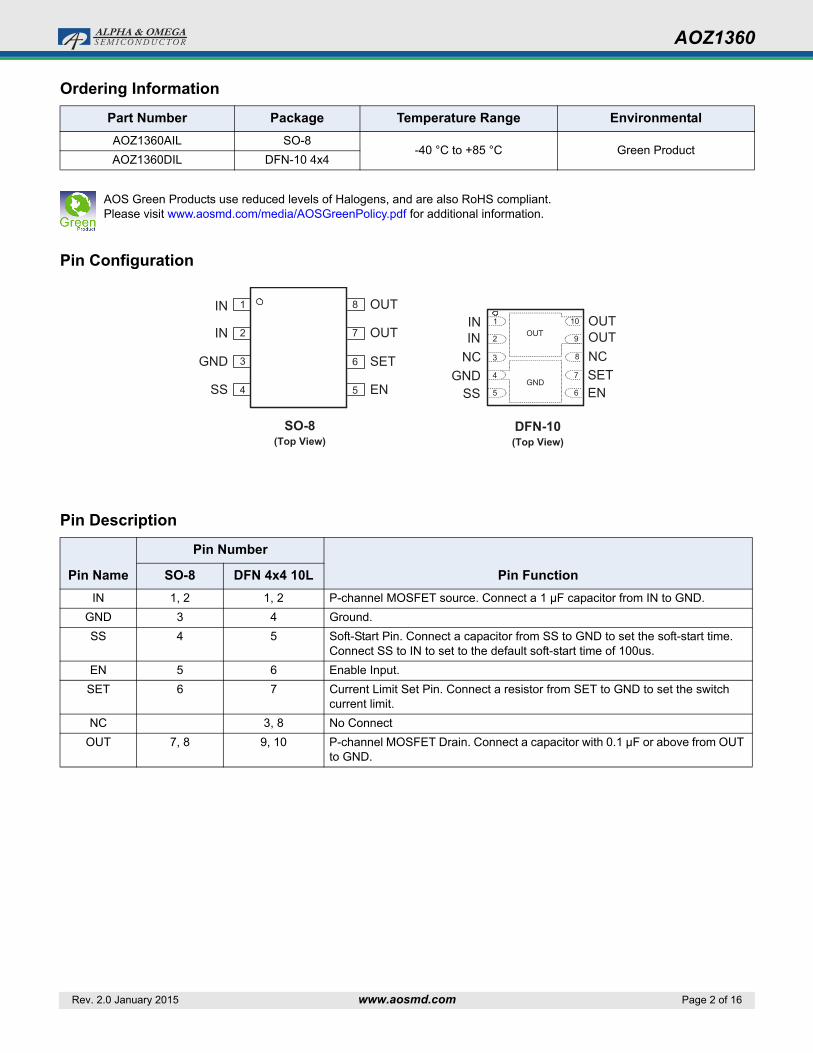
Pin Configuration
Pin Description
Part Number Package Temperature Range Environmental
AOZ1360AIL SO-8-40 °C to +85 °C Green Product
AOZ1360DIL DFN-10 4x4
Pin Name
Pin Number
Pin FunctionSO-8 DFN 4x4 10L
IN 1, 2 1, 2 P-channel MOSFET source. Connect a 1 µF capacitor from IN to GND.
GND 3 4 Ground.
SS 4 5 Soft-Start Pin. Connect a capacitor from SS to GND to set the soft-start time. Connect SS to IN to set to the default soft-start time of 100us.
EN 5 6 Enable Input.
SET 6 7 Current Limit Set Pin. Connect a resistor from SET to GND to set the switch current limit.
NC 3, 8 No Connect
OUT 7, 8 9, 10 P-channel MOSFET Drain. Connect a capacitor with 0.1 µF or above from OUT to GND.
SO-8(Top View)
DFN-10(Top View)
IN
IN
NESS
OUT1
2
8
GND 3
OUT7
SET6
4 5
ININ
SS EN
OUT
GND
OUT
SETNC NC
1
2
4
6
9
3 8
7
5
10
GND
OUT
AOZ1360
Rev. 2.0 January 2015 www.aosmd.com Page 3 of 16
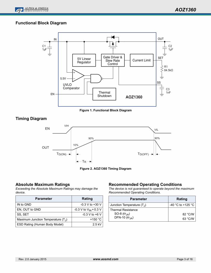
Functional Block Diagram
Figure 1. Functional Block Diagram
Timing Diagram
Figure 2. AOZ1360 Timing Diagram
Absolute Maximum RatingsExceeding the Absolute Maximum Ratings may damage the device.
Recommended Operating ConditionsThe device is not guaranteed to operate beyond the maximum Recommended Operating Conditions.
IN OUT
SET
SS
EN
5.5V
Gate Driver &Slew Rate
Control
5V LinearRegulator
ThermalShutdown
Current Limit
UVLOComparator
AOZ1360
C11μF
C2
R184.5kΩ
1μF
C31nF
10%
90% 90%
VIL
VIHEN
TD(ON)
TR
OUT
TD(OFF)
Parameter Rating
IN to GND -0.3 V to +30 V
EN, OUT to GND -0.3 V to VIN + 0.3 V
SS, SET -0.3 V to +6 V
Maximum Junction Temperature (TJ) +150 °C
ESD Rating (Human Body Model) 2.5 kV
Parameter Rating
Junction Temperature (TJ) -40 °C to +125 °C
Thermal Resistance SO-8 (JA) DFN-10 (JA)
82 °C/W
63 °C/W

AOZ1360
Rev. 2.0 January 2015 www.aosmd.com Page 4 of 16
Electrical CharacteristicsVIN = 12V, TA = 25°C unless otherwise stated.
Symbol Parameter Conditions Min. Typ. Max Units
VIN Input Supply Voltage 5.5 28 V
VUVLO Undervoltage Lockout Threshold
IN rising 4.9 5.4 V
VUVHYS Undervoltage Lockout Hysteresis
400 mV
IIN_ON Input Quiescent Current EN = IN, no load 220 400 A
IIN_OFF Input Shutdown Current EN = GND, no load 1 A
ILEAK Output Leakage Current EN = GND, no load 1 A
RDS(ON) Switch On Resistance AOZ1360AI VIN = 12 V 22 35 m
RDS(ON) Switch On Resistance AOZ1360AI VIN = 5.5 V 33 43 m
ILIM Current Limit RSET = 84.5 k 2 2.7 3.4 A
VEN_L Enable Input Low Voltage 0.8 V
VEN_H Enable Input High Voltage 2.0 V
VEN_HYS Enable Input Hysteresis 100 mV
IEN_BIAS Enable Input Bias Current 1 A
Td_on Turn-On Delay TimeEN_50% to OUT_10%
RL = 120 , CL = 1 F, SS = Floated 220 s
tON Turn-On Rise TimeOUT_10% to 90%
RL = 120 , CL = 1 F, SS = Floated 280 s
RL = 120 , CL = 1 F, CSS = 1 nF 360
tOFF Turn-Off Fall Time RL = 120 , CL = 1 F, SS = Floated 280 s
TSD Thermal Shutdown Threshold 130 C
TSD_HYS Thermal Shutdown Hysteresis 30 C
AOZ1360
Rev. 2.0 January 2015 www.aosmd.com Page 5 of 16
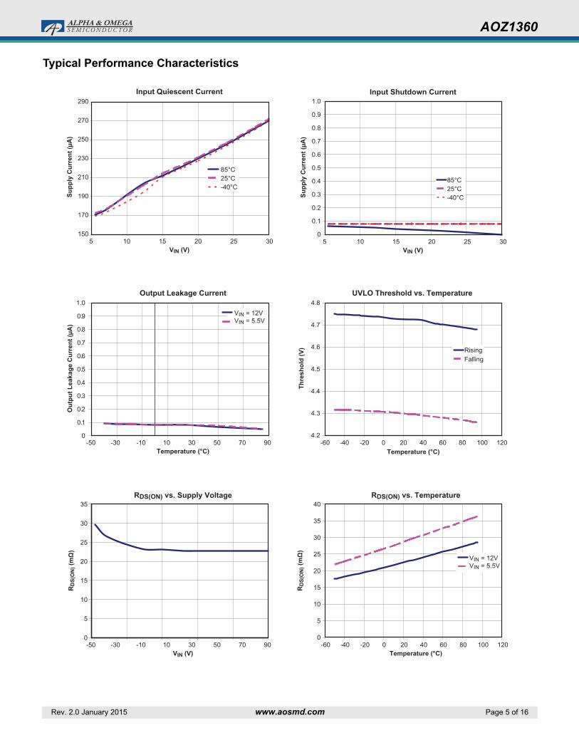
Typical Performance Characteristics
150
170
190
210
230
250
270
290
5 10 15 20VIN (V)
Input Quiescent Current
Supp
ly C
urre
nt (μ
A)
25 30
0
0.1
0.2
0.3
0.4
0.5
0.6
0.7
0.8
0.9
1.0
85°C25°C-40°C
85°C25°C-40°C
0
0.1
0.2
0.3
0.4
0.5
0.6
0.7
0.8
0.9
1.0
4.2
4.3
4.4
4.5
4.6
4.7
4.8
-60 -40 -20 0 20 40 60 80 100 120
RisingFalling
0
5
10
15
20
25
30
35
0
5
10
15
20
25
30
35
40
-60 -40 -20 0 20 40 60 80 100 120
5 10 15 20VIN (V)
Input Shutdown Current
Supp
ly C
urre
nt (μ
A)
25 30
VIN = 12VVIN = 5.5V
10 30 50 70 90-10-30-50Temperature (°C)
Output Leakage Current
Out
put L
eaka
ge C
urre
nt (μ
A)
10 30 50 70 90-10-30-50VIN (V)
RDS(ON) vs. Supply Voltage
RD
S(O
N) (
mΩ
)
Temperature (°C)
RDS(ON) vs. Temperature
RD
S(O
N) (
mΩ
)
Temperature (°C)
UVLO Threshold vs. TemperatureTh
resh
old
(V)
VIN = 12VVIN = 5.5V
AOZ1360
Rev. 2.0 January 2015 www.aosmd.com Page 6 of 16
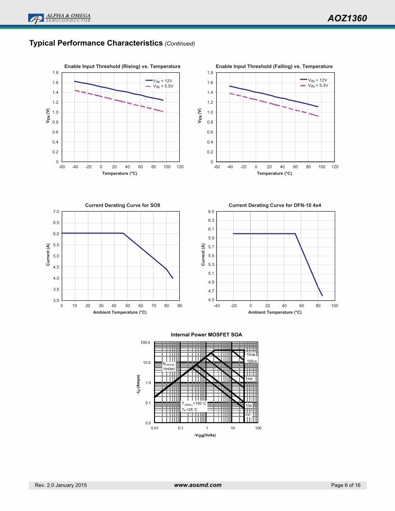
Typical Performance Characteristics (Continued)
0
0.2
0.4
0.6
0.8
1.0
1.2
1.4
1.6
1.8
0
0.2
0.4
0.6
0.8
1.0
1.2
1.4
1.6
1.8
-60 -40 -20 0 20 40 60 80 100 120
Enable Input Threshold (Rising) vs. Temperature
V EN
(V)
Enable Input Threshold (Falling) vs. Temperature
V EN
(V)
Temperature (°C)-60 -40 -20 0 20 40 60 80 100 120
Temperature (°C)
VIN = 12VVIN = 5.5V
VIN = 12VVIN = 5.5V
7.0
6.5
6.0
5.5
5.0
4.5
4.0
3.5
3.0
6.5
6.3
6.1
5.9
5.7
5.5
5.3
5.1
4.9
4.7
4.50 10 20 30 40 50 60 70 80 90
Current Derating Curve for SO8 Current Derating Curve for DFN-10 4x4
Cur
rent
(A)
Ambient Temperature (°C)
Cur
rent
(A)
Ambient Temperature (°C)-40 -20 0 20 40 60 80 100
0.0
0.1
1.0
10.0
100.0
0.01 0.1 1 10 100
-ID
(Am
ps)
-VDS(Volts)
10ms
10s
1ms
DC
RDS(ON)
limited
TJ(Max) =150 CTA =25 C
100m
Internal Power MOSFET SOA
AOZ1360
Rev. 2.0 January 2015 www.aosmd.com Page 7 of 16
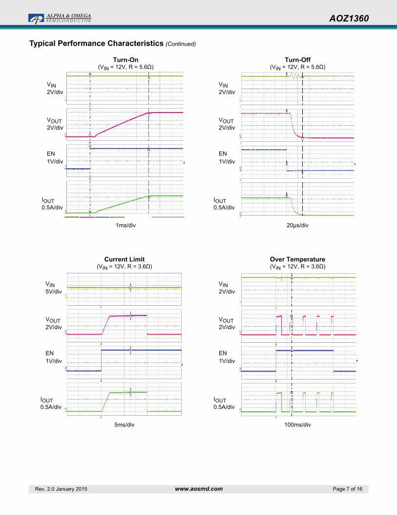
Typical Performance Characteristics (Continued)
Turn-On(VIN = 12V, R = 5.6Ω)
1ms/div
VIN2V/div
VOUT2V/div
EN1V/div
IOUT0.5A/div
Turn-Off(VIN = 12V, R = 5.6Ω)
20μs/div
VIN2V/div
VOUT2V/div
EN1V/div
IOUT0.5A/div
Over Temperature(VIN = 12V, R = 3.6Ω)
100ms/div
VIN2V/div
VOUT2V/div
EN1V/div
IOUT0.5A/div
Current Limit(VIN = 12V, R = 3.6Ω)
5ms/div
VIN5V/div
VOUT2V/div
EN1V/div
IOUT0.5A/div

AOZ1360
Rev. 2.0 January 2015 www.aosmd.com Page 8 of 16
Detailed Description
Introduction
The AOZ1360 is a 35 m P-channel high-side load switch with adjustable soft-start slew-rate control, programmable current limit and thermal shutdown. It operates with an input voltage range from 5.5 V to 28 V.
Enable
The EN pin is the On/Off control for the output switch.It is an active-high input. The EN pin is active after VIN is above the UVLO threshold of 4.9 V. Conversely, the EN pin will be deactivated if the VIN falls below the UVLO of 2.0V. The EN pin must be driven to a logic high or logic low state to guarantee operation. While disabled, the AOZ1360 only draws approximately 1 µA supply current. The EN is a high impedance input with an ESD protection diode to ground and should not be forced below ground. This input level is compatible with most microcontroller outputs and other logic families.
Under-Voltage Lockout (UVLO)
The under-voltage lockout (UVLO) circuit of the AOZ1360 monitors the input voltage and prevents the output MOSFET from turning on until VIN exceeds 4.9 V.
Adjustable Soft-Start Slew-Rate Control
When the EN pin is high, the slew rate control circuitry applies voltage on the gate of the PMOS switch in a manner such that the output voltage and current is ramped up linearly until it reaches the steady-state load current level. The slew rate can be adjusted by an external capacitor connected between the SS pin and ground.
The slew rate rise time, Ton, can be set using the following equation:
Programmable Current Limit
The current limit is programmed by an external resistor connected between the SET pin and ground. This sets a reference voltage to the current limit error amplifier that compares it to a sensed voltage that is generated by passing a small portion of the load current through an internal amplifier. When the sensed load current exceeds the set current limit, the load current is then clamped at the set limit and the Vout drops to whatever voltage is necessary to clamp the load current. The AOZ1360 will stay in this condition until the load current no longer exceeds the current limit or if the thermal shutdown protection is engaged.
Thermal-Shutdown Protection
During current limit or short circuit conditions, the PMOS resistance is increased to clamp the load current. This increases the power dissipation in the chip causing the die temperature to rise. When the die temperature reaches 130 °C the thermal shutdown circuitry will shutdown the device. There is a 30 °C hysteresis after which the device will turn back on and go through soft start. The thermal shutdown will cycle repeatedly until the short circuit condition is resolved or the enable pin is pulled LOW externally.
TonCss VIN
30A--------------------------=

AOZ1360
Rev. 2.0 January 2015 www.aosmd.com Page 9 of 16
Application Information
Input Capacitor Selection
The input capacitor prevents large voltage transients from appearing at the input and provides the instantaneous current needed each time the switch turns on. The input capacitor also limits input voltage drop and prevents high-frequency noise on the power line from passing through the output of the power side. The choice of input capacitor is based on its ripple current and voltage ratings rather than the actual capacitance value. The input capacitor should be located as close to VIN as possible. A 1 µF ceramic cap is recommended. However, higher capacitor values will further reduce the voltage drop at the input.
Output Capacitor Selection
The output capacitor acts in a similar way. A small 0.1 µF capacitor prevents high-frequency noise from going into the system. Also, the output capacitor has to supply enough current for any large load that may occur during system transients. This bulk capacitor must be large enough to supply fast transient load in order to prevent the output from dropping.
Current Limit Setting
The current limit is set by an external resistor connected to the SET pin. Refer to Figure 3 for current limit settings.
Figure 3
Slew Rate Setting
Slew rate is set by changing the capacitor value on the SS pin of the device. A capacitor connected between the SS pin and ground will reduce the output slew-rate. The capacitive range is 0.001 µF to 0.1 µF. Refer to Figure 4.
Figure 4. Output Slew Rate Adjustment vs. Capacitance
Power Dissipation Calculation
Calculate the power dissipation for normal load condition using the following equation:
PD = RON x (IOUT)2
The worst case power dissipation occurs when the load current hits the current limit due to over-current or short circuit faults. The power dissipation under these conditions can be calculated using the following equation:
PD = (VIN – VOUT) x ILIMIT
7
6
5
4
3
2
1
035 45 55 65 75 85 95 105
AOZ1360 Rset vs ILIM
ILIM (A)
RSET (kΩ)
0
5
10
15
20
25
30
35
40
45
0 0.02 0.04 0.06 0.08 0.1Capacitance (μF)
Slew Rate(ms)

AOZ1360
Rev. 2.0 January 2015 www.aosmd.com Page 10 of 16
Layout GuidelinesProper PCB layout is important for improving the thermal and overall performance of the AOZ1360. To optimize the switch response time for outputting short-circuit conditions, keep all traces as short as possible. This will also reduce the effect of unwanted parasitic inductance.
Place the input and output bypass capacitors as close as possible to the IN and OUT pins. The input and output PCB traces should be as wide as possible for the given PCB space. Use a ground plane to enhance the power dissipation capability of the device.
Figure 5. AOZ1360AI (SO-8) Layout Figure 6. AOZ1360DI (DFN4x4 10L) Layout
C2C1
C3
R1
1
2
4
6
9
3 8
7
10
NC
OUT
OUT
NC
OUT
GNDGND
IN
IN
SET
ENGND
5SS
C2C1
GND
GND
EN
3
5
7
OUT
2
1
IN
IN
OUT
8
C3
R1SS
SET
4
6

AOZ1360
Rev. 2.0 January 2015 www.aosmd.com Page 11 of 16
Package Dimensions, SO-8L
Notes:1. All dimensions are in millimeters.2. Dimensions are inclusive of plating3. Package body sizes exclude mold flash and gate burrs. Mold flash at the non-lead sides should be less than 6 mils.4. Dimension L is measured in gauge plane.5. Controlling dimension is millimeter, converted inch dimensions are not necessarily exact.
SymbolsAA1A2bcDEe
E1hLθ
Dimensions in millimetersRECOMMENDED LAND PATTERN
Min.1.350.101.250.310.174.803.80
5.800.250.400°
D
C
L
h x 45
7 (4x)
b
2.20
2.87
5.74
0.800.635 UNIT: mm
1.27
A1
A2 A0.1
θ
Gauge Plane Seating Plane
0.25e8
1
EE1
Nom.1.65—
1.50——
4.903.90
1.27 BSC6.00———
Max.1.750.251.650.510.255.004.00
6.200.501.278°
SymbolsA
A1A2bcDEe
E1hLθ
Dimensions in inchesMin.0.0530.0040.0490.0120.0070.1890.150
0.2280.0100.016
0°
Nom.0.065
—0.059
——
0.1930.154
0.050 BSC0.236
———
Max.0.0690.0100.0650.0200.0100.1970.157
0.2440.0200.050
8°
AOZ1360
Rev. 2.0 January 2015 www.aosmd.com Page 12 of 16
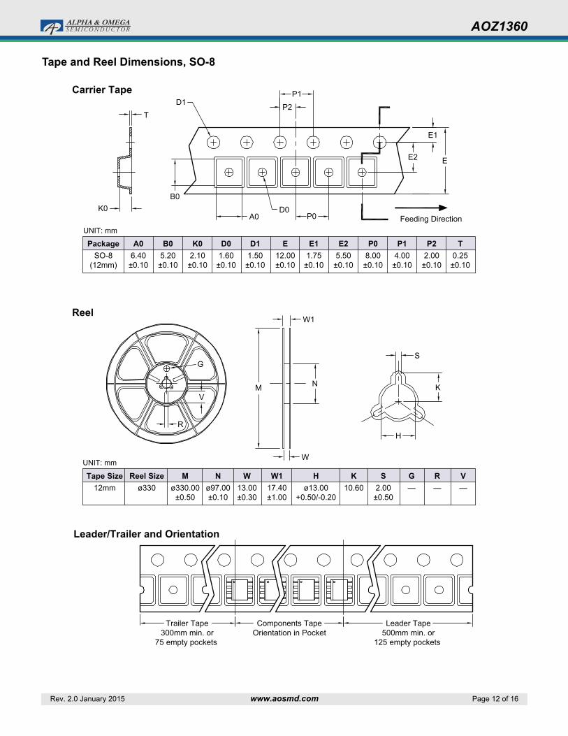
Tape and Reel Dimensions, SO-8
Carrier Tape
Reel
Tape Size12mm
Reel Sizeø330
Mø330.00
±0.50
PackageSO-8
(12mm)
A06.40±0.10
B05.20±0.10
K02.10±0.10
D01.60±0.10
D11.50±0.10
E12.00±0.10
E11.75±0.10
E25.50±0.10
P08.00±0.10
P14.00±0.10
P22.00±0.10
T0.25±0.10
Nø97.00±0.10
K0
UNIT: mm
B0
G
M
W1
S
K
H
N
W
V
R
Trailer Tape300mm min. or
75 empty pockets
Components TapeOrientation in Pocket
Leader Tape500mm min. or
125 empty pockets
A0
P1
P2
Feeding DirectionP0
E2
E1
E
D0
TD1
W13.00±0.30
W117.40±1.00
Hø13.00
+0.50/-0.20
K10.60
S2.00±0.50
G—
R—
V—
Leader/Trailer and Orientation
UNIT: mm

AOZ1360
Rev. 2.0 January 2015 www.aosmd.com Page 13 of 16
Package Dimensions, DFN-10L, 4x4
SeatingPlane
BA
C
4
6
5
3
2
Notes:
1. All dimensions are in millimeters.2. The dimensions with * are just for reference.
3. The location of the terminal #1 identifier and terminal numbering convention conforms to JEDEC publication 95 SPP-002.
4. Dimension b applies to metallized terminal and is measured between 0.15mm and 0.30mm from the terminal tip. If the terminal has the optional radius on the other end of the terminal, then dimension b should not be measured in that radius area.
5. Coplanarity applies to the terminals and all other bottom surface metallization.
6. Drawings shown are for illustration only.
ddd
eee
b
e
L
E1
D2
A1A
A3
D1
Pin #1 IDA
L1
L3
10x
INDEX AREA(D/2xE/2)
Chamfer 0.20
Unit: mm
*
L4
L4
*
0.35 TYP
0.38
*
6 10
Pin 1
D/2
D/2
D
E
15
5 1
10 6
Chamfer 0.20
0.02
Pin #1 IDA
1.78 1.42
0.30
0.30
2.30
0.65 Typ.0.65 Typ.
1.153.55
E1/2
L2
TOP VIEW BOTTOM VIEW
SIDE VIEW
RECOMMENDED LAND PATTERN
SymbolsA
A1A3bD
D1D2E
E1eL
L1L2L3L4
aaabbbcccdddeee
Dimensions in millimetersMin.0.700.00
0.303.951.581.223.952.20
0.50—
0.28
Nom.0.750.02
0.203 REF0.354.001.681.324.002.30
0.65 BSC0.550.020.38
0.85 REF0.30 REF
0.150.100.100.080.05
Max.0.800.05
0.404.051.781.424.052.40
0.600.120.48
SymbolsA
A1A3bD
D1D2E
E1eL
L1L2L3L4
aaabbbcccdddeee
Dimensions in inchesMin.0.0280.000
0.0120.1560.0620.0480.1560.087
0.020—
0.011
Nom.0.0300.001
0.008 REF0.0140.1570.0660.0520.1570.091
0.026 BSC0.0220.0010.015
0.033 REF.0.012 REF
0.0060.0040.0040.0030.002
Max.0.0310.002
0.0160.1590.0700.0560.1590.094
0.0240.0050.019

AOZ1360
Rev. 2.0 January 2015 www.aosmd.com Page 14 of 16
Tape and Reel Dimensions, DFN-10L, 4x4
PackageDFN 4x4(12mm)
A0 B0 K0 E E1 E2D0 D1 P0 P1 P2 T4.35
±0.10 ±0.101.10
Min.1.50 1.50
+0.1/-0.0 ±0.312.0
±0.101.75
±0.055.50
±0.108.00
±0.104.00
±0.052.00
±0.050.30
R
VM
N
GS
WNM
ø79.0ø330.0±2.0
12.412 mm
Tape Size VRSK
±0.52.010.5
G
— — —
HW1
ø13.0±0.5
17.0
H
K
W
W1
Reel Sizeø330
UNIT: MM
UNIT: MM
±1.0 +2.0/-0.0 +2.6/-0.0
D1 P1
E1
E2E
P2
K0
T
A0P0
B0
D0
CL
±0.2
±0.104.35
Carrier Tape
Reel
Trailer Tape300mm min. or
75 empty pockets
Components TapeOrientation in Pocket
Leader Tape500mm min. or
125 empty pockets
Leader/Trailer and Orientation
Feeding Direction
AOZ1360
Rev. 2.0 January 2015 www.aosmd.com Page 15 of 16
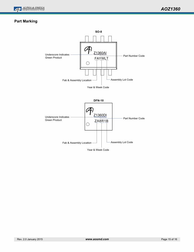
Part Marking
Z1360AI FAY
Part Number Code
Assembly Lot CodeFab & Assembly Location
Year & Week Code
WLT
Underscore Indicates Green Product
SO-8
Z1360DI
ZA8R1BPart Number Code
Assembly Lot CodeFab & Assembly Location
Year & Week Code
DFN-10
Underscore Indicates Green Product

AOZ1360
Rev. 2.0 January 2015 www.aosmd.com Page 16 of 16
As used herein:
1. Life support devices or systems are devices or systems which, (a) are intended for surgical implant into the body or (b) support or sustain life, and (c) whose failure to perform when properly used in accordance with instructions for use provided in the labeling, can be reasonably expected to result in a significant injury of the user.
2. A critical component in any component of a life support, device, or system whose failure to perform can be reasonably expected to cause the failure of the life support device or system, or to affect its safety or effectiveness.
LEGAL DISCLAIMER
Alpha and Omega Semiconductor makes no representations or warranties with respect to the accuracy or completeness of the information provided herein and takes no liabilities for the consequences of use of such information or any product described herein. Alpha and Omega Semiconductor reserves the right to make changes to such information at any time without further notice. This document does not constitute the grant of any intellectual property rights or representation of non-infringement of any third party’s intellectual property rights.
LIFE SUPPORT POLICY
ALPHA AND OMEGA SEMICONDUCTOR PRODUCTS ARE NOT AUTHORIZED FOR USE AS CRITICAL COMPONENTS IN LIFE SUPPORT DEVICES OR SYSTEMS.


![THz Communications An Option for Wireless Networks …¼rner.pdf0.2 0.4 0.6 0.8 1 eit Oberflächenhöhe [mm] Raufaser 100 150 200 250 300 350 400 450 0 0.2 0.4 0.6 0.8 1 f [GHz] or](https://static.fdocuments.in/doc/165x107/5ee176cbad6a402d666c5672/thz-communications-an-option-for-wireless-networks-rnerpdf-02-04-06-08-1-eit.jpg)