ANSYS for Computer - ANSYS Customer Portal Login for Tablet Computer Design Presenter name: Greg...
43
© 2011 ANSYS, Inc. October 12, 2011 1 ANSYS for Tablet Computer Design Presenter name: Greg Pitner
-
Upload
phungnguyet -
Category
Documents
-
view
229 -
download
3
Transcript of ANSYS for Computer - ANSYS Customer Portal Login for Tablet Computer Design Presenter name: Greg...

© 2011 ANSYS, Inc. October 12, 20111
ANSYS for Tablet Computer Design
Presenter name: Greg Pitner

© 2011 ANSYS, Inc. October 12, 20112
• Shopping, reading, emailing, accessing social network, playing games
• Schools, operating rooms, sports events
Tablets in our daily lives
Pictures source: www.istockphoto.com

© 2011 ANSYS, Inc. October 12, 20113
ProblemPredict the performance of a tablet design while meeting strict electrical standards and design specifications
SolutionAutomated modeling and optimized analysis using ANSYS Electromagnetics tools allows for system simulation approach
ResultDetailed and accurate system simulation approach enables tablets to be put on market on time with reduced testing costs
ANSYS for Tablet Designs
Pictures source: www.istockphoto.com

© 2011 ANSYS, Inc. October 12, 20114
3D CAD
Layout
Virtual Prototype
Vendor SpecificDriver/Receiver Models
Vendor SpecificVRM Models
Electronics
Virtual Compliance
VirtualSystem
ElectromagneticExtraction
Mechanical andThermal
Virtual System Prototyping

© 2011 ANSYS, Inc. October 12, 20115
Design Aspects• Touchscreen• Tablet Case• Packages • Flex circuitry• Antenna• ESD• EMI
Tablets Design Challenges

© 2011 ANSYS, Inc. October 12, 20116
Design Aspects• Touchscreen• Tablet Case• Packages • Flex circuitry• Antenna• ESD• EMI
Tablets Design Challenges

© 2011 ANSYS, Inc. October 12, 20117
No moving parts present • Use a thin layer of ITO (indium tin oxide) to sense the presence of a finger by capacitive coupling.
• Capacitive sensors are mounted underneath of hardened glass • Finger adds a measurable capacitive change in the touch sensor• Change in sensor capacitance relies on RC time constant change
Capacitive Touchscreen

© 2011 ANSYS, Inc. October 12, 20118
Model size, complexity and ….• Simulate “projected” and/or “mutual‐capacitance”• Include Skin and Proximity Effects• Build detailed 3D model
Touchscreen Design Challenges

© 2011 ANSYS, Inc. October 12, 20119
Parameterized Example 10x10 electrodes model
Capacitive Touchscreen

© 2011 ANSYS, Inc. October 12, 201110
Adaptive Mesh Refinement• Automatically tunes the mesh to the electrical performance of the
device. This ensures simulations are correct the first time.
Mesh Convergence• Real‐Time update of performance per adaptive solution
Automatic and Robust Adaptive Meshing
Initial Mesh
Refined Mesh
© 2011 ANSYS, Inc. October 12, 201111
Accuracy of Q3D Capacitance solution• Automated Meshing Refinement
Capacitive Touchscreen

© 2011 ANSYS, Inc. October 12, 201112
RLGC values, including coupling effects
Solution Time (10x10 electrodes model)• 2 hrs 45 min• Supports all available cores
Results
© 2011 ANSYS, Inc. October 12, 201113
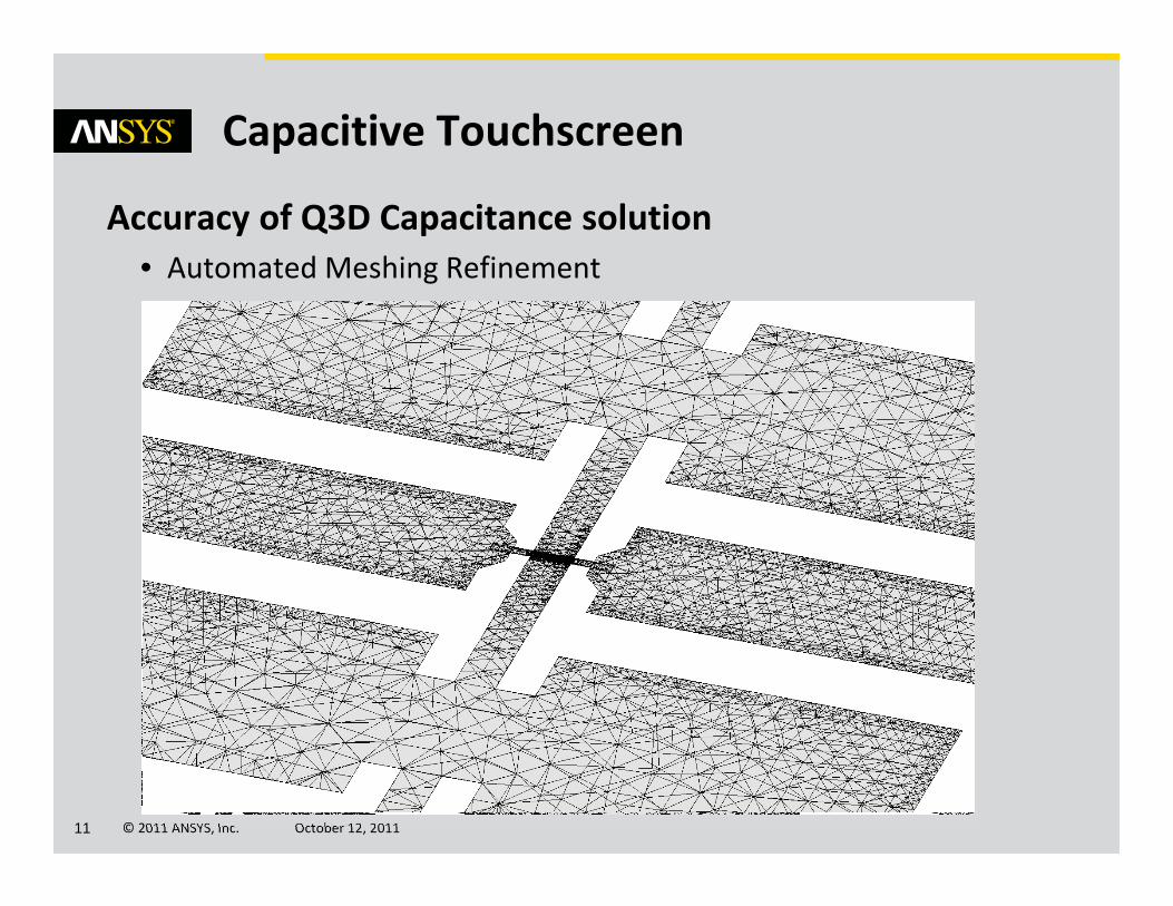
Focus on• Area of contact • Glass thickness
Finger Tip Effect

© 2011 ANSYS, Inc. October 12, 201114
Receiver Signal
Electrode scanning change at contacted ITO (Indium Tin Oxide) position
Non‐contact
Proximity Effects (0.1mmGap)
Contact!

© 2011 ANSYS, Inc. October 12, 201115
Design Aspects• Touchscreen• Tablet Case• Packages • Flex circuitry• Antenna• ESD• EMI
Tablets Design Challenges

© 2011 ANSYS, Inc. October 12, 201116
• Perform Drop test of Tablet PC from height of 4 feet onto a concrete floor at an angle of 45 degree using ANSYS Explicit Dynamics
• The geometry of the Table PC was created from scratch using ANSYS DesignModeler• The parts are simplified representations of parts in an actual Tablet PC.
Tablet Computer Case

© 2011 ANSYS, Inc. October 12, 201117
• The geometry of the Table PC was created from scratch using ANSYS DesignModeler
Tablet Case Project Schematic

© 2011 ANSYS, Inc. October 12, 201118
• Meshing:– ANSYS Workbench meshing with Explicit Dynamics preference is used to create a mesh.
– Total number of elements ~25,000
• Analysis settings:– Analysis is solved for 4 e‐4 seconds.– Initial velocity of 4.9 m/sec is assigned to the Tablet
– Parts that are in contact but may separate due to the drop test are assigned bonded contacts.
– Bonded contacts are modeled as breakable based on stress criteria for debonding.
Drop test

© 2011 ANSYS, Inc. October 12, 201119
Equivalent Stress Contours Back Cover Off
Equivalent Stress Contours Front
Drop Test Simulation Results

© 2011 ANSYS, Inc. October 12, 201120
Stress Modeling using ANSYS Mechanical includes• Joints to capture the kinematics• Visco‐elastic material• Contact non‐linearity• Rigid flexible interaction
Stress Modeling Analysis

© 2011 ANSYS, Inc. October 12, 201121
Design Aspects• Touchscreen• Tablet Case• Packages• Flex circuitry• Antenna• ESD• EMI
Tablets Design Challenges
© 2011 ANSYS, Inc. October 12, 201122
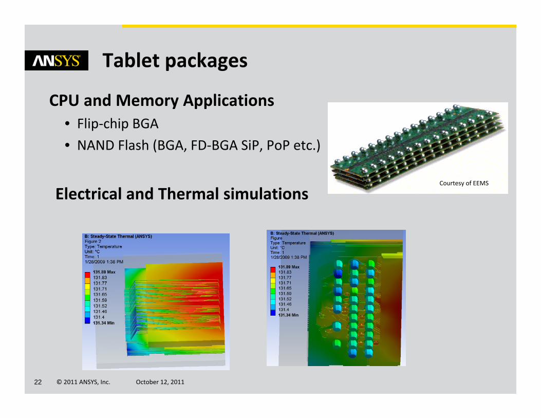
CPU and Memory Applications• Flip‐chip BGA• NAND Flash (BGA, FD‐BGA SiP, PoP etc.)
Electrical and Thermal simulations
Tablet packages
Courtesy of EEMS

© 2011 ANSYS, Inc. October 12, 201123
Design Challenges• Accurate SYZ and RLGC solution• Dealing with multiple vendors
Solution• Automated merging capabilities• Full‐wave and Quasi‐static solution
Tablet packages
Courtesy of EEMS

© 2011 ANSYS, Inc. October 12, 201124
Inside of Cadence SiP and APD and Allegro• Setup of the HFSS ready to solve project in the Cadence environment• Signal and pwr/gnd net selection• Auto port creation on solderballs and bumps/bondwires• Plane Extent and HFSS Solution Setup Options
HFSS in Cadence
HFSS Solution in progress
© 2011 ANSYS, Inc. October 12, 201125
Design Aspects• Touchscreen• Tablet Case• Packages • Flex circuitry• Antenna• ESD• EMI
Tablets Design Challenges

© 2011 ANSYS, Inc. October 12, 201126
Parameterized Transmission line model• Accurate Zo analysis• Trace spacing and offsets• Solid vs. patterned ground
FLEX circuit analysis
HFSS Transient

© 2011 ANSYS, Inc. October 12, 201127
Interconnect Transmission line model• Trace Thickness and Width• Trace to Ground Space• Ground Shape (Solid vs. Meshed)
– Reduce the Interference with High Speed signal Traces or noisy LCD surface
FLEX circuit analysis

© 2011 ANSYS, Inc. October 12, 201128
Flex Optimization analysis• Impact of multiple variables on overall designs• Goal driven optimization
Design of Experiments
Parametric HFSS Design
WB DX Setup
Response Surface ‐ TDR

© 2011 ANSYS, Inc. October 12, 201129
Design Aspects• Touchscreen• Tablet Case• Packages • Flex circuitry• Antenna• ESD• EMI
Tablets Design Challenges

© 2011 ANSYS, Inc. October 12, 201130
Antenna Design Challenges• Location, Beam Forming• Antenna type• Human Body Effect
– Hand, Body
• Operation Environments– Metal Desk– Wooden Desk– Human lap
Tablet Antenna

© 2011 ANSYS, Inc. October 12, 201131
Antenna Design Challenges• Location, Beam Forming• Human Body Effect
– Hand holding tablet at different locations– Close to antenna and away from antenna
Tablet Antenna
Radiation Efficiency @2.4Ghz :0.967907 Radiation Efficiency @2.4Ghz : 0.480466

© 2011 ANSYS, Inc. October 12, 201132
Antenna Design Challenges• Operation Environments
– Human Tissue– Metal Desk– Wooden Desk
Tablet Antenna
Human Tissue Metal Desk
Wooden Desk
Radiation Efficiency @2.4Ghz : 0.994337
Radiation Efficiency @2.4Ghz : 0.993303Radiation Efficiency @2.4Ghz : 0.777207

© 2011 ANSYS, Inc. October 12, 201133
Design Aspects• Touchscreen• Tablet Case• Packages • Flex circuitry• Antenna• ESD• EMI
Tablets Design Challenges

© 2011 ANSYS, Inc. October 12, 201134
Circuit and Numerical Modeling of ESD Coupling to Shielded CablesHFSS Transient solver for numerical Modeling ESD approach
0.00 5.00 10.00 15.00 20.00 25.00 30.00Time [ns]
-1.00
0.00
1.00
2.00
3.00
4.00
5.00
6.00
V(Vo
ltage
1) [k
V]
HFSSDesign1Input Voltage ANSOFT
Curve InfoV(Voltage1)
Setup1 : Transient
ESD Analysis
Courtesy of: HUWIN

© 2011 ANSYS, Inc. October 12, 201135
ESD Gun Simulation Results
0.00 10.00 20.00 30.00 40.00 50.00 60.00Time [ns]
0.00
5.00
10.00
15.00
20.00
25.00
Cur
rent
(A) [
A]
HFSSDesign1Peak Current VS Applied Voltage ANSOFT
Curve Infomag(I(R1,Voltage1))
Importedmag(I(R1,Voltage1))_1
Importedmag(I(R1,Voltage1))_2
Importedmag(I(R1,Voltage1))_3
Imported
: 6kV: 5kV: 4kV: 2kV
Applied Voltage (kV)
Peak Current (A)IEC 61000‐4‐2 (ESD Test)
Peak Current (A)Simulation Results
2 7.5 7.754 15 15.55 18.75 19.36 22.5 23.25
Courtesy of: HUWIN

© 2011 ANSYS, Inc. October 12, 201136
ESD Gun Simualtion Time length:0 ns ~ 118 ns
ESD Gun and Metal Plate
ESD Animation
Courtesy of: HUWIN

© 2011 ANSYS, Inc. October 12, 201137
ESD gun applied on 1 driver and 1 receiver full length electrode
ESD Gun on Tablets touch electrodes

© 2011 ANSYS, Inc. October 12, 201138
ESD Gun Simulation Time length:0 ns ~ 118 ns
ESD Gun effect on Tablets touch electrodes

© 2011 ANSYS, Inc. October 12, 201139
ESD Current
ESD Gun current injected on touch electrodes

© 2011 ANSYS, Inc. October 12, 201140
Design Aspects• Touchscreen• Tablet Case• Packages • Flex circuitry• Antenna• ESD• EMI
Tablets Design Challenges

© 2011 ANSYS, Inc. October 12, 201141
EMI Design Challenges• Entire PCB + Case• Driver & Receiver• Near field, Farfield• Immunity
Tablet EMI
: Digital source Termination
Slot
=
+

© 2011 ANSYS, Inc. October 12, 201142
EMI Design Results• Near Field and Far Field Spectrum
Tablet EMI
Simulation vs. Measurement
Simulation
Measurement

© 2011 ANSYS, Inc. October 12, 201143
Tablet Design Simulations were performed using• Touchscreen – Q3D Extractor and DesignerSI• Tablet Case – ANSYS Explicit Dynamic and ANSYS Mechanical• Packages –
– Electrical: HFSS in Cadence, Q3D Extractor and TPA– Thermal: ANSYS Icepak
• Flex circuitry – HFSS and Q3D Extractor• Antenna ‐ HFSS• ESD ‐ HFSS Transient and DesignerSI• EMI – HFSS, SIwave and DesignerSI
Tablets Design Solution