
ANNUAL REPORT 2017 - JARA
171
AN INITIATIVE OF ANNUAL REPORT 2017 Fundamentals of Future Information Technology
Transcript of ANNUAL REPORT 2017 - JARA

AN INITIATIVE OF
ANNUAL REPORT 2017Fundamentals of Future Information Technology
Annu
al R
epor
t 201
7
JARA-FIT Jülich Aachen Research Alliancefor Fundamentals of Future Information Technology
OFFICEForschungszentrum Jülich GmbH | 52425 Jülich, GermanyPhone: ++49-2461-61-3107 | Email: [email protected]

Publication Details
JARA-FITJülich Aachen Research Alliancefor Fundamentals of Future Information TechnologyAnnual Report 2017
Published by:Forschungszentrum Jülich GmbH, 52425 JülichRWTH Aachen University, 52062 Aachen
Publication supported by the Excellence Initiative of the German federal and state governments.
Editors:Dr. Wolfgang SpeierManaging Director JARA-FITForschungszentrum Jülich GmbH52425 JülichGermanyPhone: ++49-2461-61-3107
Prof. Dr. Stefan TautzScientific Director JARA-FITPeter Grünberg Institute – Functional Nanostructures at Surfaces Forschungszentrum Jülich GmbH52425 JülichGermanyPhone: ++49-2461-61-4561
Prof. Dr. Matthias Wuttig Scientific Director JARA-FIT I. Institute of Physics A RWTH Aachen University 52074 Aachen Germany Phone: ++49-241-8027155
Contact:Dr. Wolfgang [email protected]
Layout:Ulrike Adomeit Silke Schilling
Year of publication: 2018 Cover pictures refer to the following selected research reports (From left to right)
Background: ©Sashkin/stock.adobe.com | S. Weiß et al., Understanding the photoemission distribution of strongly interacting molecular overlayers, p. 123 | F. Lüpke et al., Electrical resistance of individual defects at a topological insulator surface, p. 101 | M. Paßens et al., Interface-driven formation of a two-dimensional dodecagonal fullerene quasicrystal, p. 55 | A. Meledin et al., Direct visualization of GeTe-Sb2Te3 superlattice defects, p. 752018

JARA-FIT Annual Report 2017
JARA-FIT Jülich Aachen Research Alliance for
Fundamentals of Future Information Technology
Annual Report 2017
Forschungszentrum Jülich
RWTH Aachen University

JARA-FIT Annual Report 2017
2

JARA-FIT Annual Report 2017
1
Dear Reader,
you hold the Xth edition of the JARA-FIT Annual Report in your hands. We look back on ten years during which JARA-FIT has established itself as the collaborative effort of the RWTH Aachen University and Forschungszentrum Jülich devoted to the field of future information technology. This has kept us pretty busy and we succeeded in attracting excellent scientists, in establishing two new joint institutes, in creating high-end facilities, in acquisition of collaborative projects, and, most important, in conducting excellent and highly visible research. In those ten years, scientists involved in JARA-FIT have received more than ten grants from the European Research Council and have become involved in two European flagship programmes. JARA-FIT has been founded in the early days of the national Excellence Initiative and we have therefore been proud to be asked to present our ideas in the context of two excellence clusters of the current round of the German Excellence Strategy. It is our firm believe that two of the major trends we envisaged, namely quantum computing and neuromorphic computing, will play an important role in the future of information technology.
The core of the booklet, which you just opened, contains short scientific reports that illustrate the work that scientists of JARA-FIT have carried out and published in 2017. By looking at the publication list at the end of the booklet you may convince yourself that these reports constitute only a small selection of what has been actually achieved. It is our hope that you will find the selected research reports an interesting read.
While being busy with our research, writing proposals or presenting our ideas, the world seemed to have come suddenly to a hold when we heard that Peter Grünberg had passed away on April 7th this year. Peter Grünberg was like a spiritus rector for us, considering his curiosity-driven personal endeavour to gain a fundamental understanding of solid state phenomena, his anticipation of the potential application of his discovery and the impact he made on information technology. Peter Grünberg received the Nobel Prize together with Albert Fert in 2007. In fact, JARA had just been founded a couple of weeks before the Nobel prize was announced. We will continue to work hard on his behalf to advance the fundamentals of future information technology. It feels just right that our institute in Jülich that explores the limits of what future information technology can achieve carries his name.
Wolfgang Speier Stefan Tautz Matthias Wuttig Managing Director Scientific Director Scientific Director

JARA-FIT Annual Report 2017
2
Contents JARA-FIT Highlights .............................................................................................. 5
General Information .......................................................................................... 11 JARA-FIT Members........................................................................................................................... 12
JARA-FIT Institutes ........................................................................................................................... 14
Selected Research Reports ................................................................................. 23 Self-assembled QDs for optical read out of spin qubits .................................................................. 25
Tunnel FETs: Toward III-V hetero-structure band-to-band tunnel FETs .......................................... 27
Effective masses, lifetimes and optical conductivity in Sr2RuO4: Spin-orbit and Coulomb interaction effects. .......................................................................................................................... 29
Unexpected Ge-Ge contacts in two-dimensional Ge4Se3Te and an analysis of their chemical cause ................................................................................................................................ 31
Antiskyrmions stabilized at interfaces by anisotropic Dzyaloshinskii-Moriya interactions ............. 33
Spin dynamics of the magnetocaloric compound MnFe4Si3 ............................................................ 35
Spin Structure of MnO Nanoparticles, powder and single crystal ................................................... 37
Magnetic excitations in the ground state of Yb2Ti2O7 ..................................................................... 39
Strain and electric-field control of magnetism in supercrystalline iron oxide nanoparticle–BaTiO3 composites .................................................................................................... 41
Atomic resolution imaging of YAlO3: Ce in the chromatic and spherical aberration corrected PICO electron microscope ............................................................................................... 43
[NiAs]-type polymorph of FeN ......................................................................................................... 45
POWTEX and multi-dimensional Rietveld refinement of neutron time-of-flight powder diffraction .......................................................................................................................... 47
2D or Not 2D: Strain tuning in weakly coupled heterostructures .................................................... 49
Pairing and chiral spin density wave instabilities on the honeycomb lattice ..................................... 51
High-resolution patterning by extreme ultraviolet interference lithography with a compact exposure tool ................................................................................................................. 53
Interface-driven formation of a two-dimensional dodecagonal fullerene quasicrystal .................. 55
Influence of ion specific effects on the immobilization of gold nanoparticles on metal surfaces ... 57
TiO2 nanoparticle monolayers: self-assembly and resistive switching ............................................ 59
Single crystalline superstructured stable single domain magnetite nanoparticles ......................... 61
Direct imaging of a zero-field target skyrmion and its polarity switch in a chiral magnetic nanodisk .......................................................................................................................... 63
Dynamical amplification of magnetoresistances and Hall currents up to the THz regime ............. 65
Entropy production in photovoltaic cell .......................................................................................... 67
CVD graphene for inverted spin valve devices fabricated by dry-transfer methods ....................... 69
Tailoring mechanically tunable strain fields in graphene ............................................................... 71
Nanosized conducting filaments formed by atomic-scale defects in redox-based resistive switching memories .......................................................................................................... 73
Direct visualization of GeTe-Sb2Te3 superlattice defects ................................................................. 75

JARA-FIT Annual Report 2017
3
Vertex parametrization for the constrained functional renormalization group .......................... 77
Viability and challenges of low–temperature control electronics for spin qubits .............................. 79
Transferring a quantum state from a photonic qubit to a gate–defined quantum dot...................... 81
Strain relaxation and ambipolar electrical transport in GaAs/InSb core-shell nanowires .............. 83
Surface space charge formation in donor doped SrTiO3 ................................................................. 85
Spectroscopic indications of tunnel barrier charging as the switching mechanism in memristive devices .......................................................................................................................... 87
Defect-control of electron transport in 2D oxide heterostructures ................................................. 89
Oxygen vacancy ordering in epitaxial double-perovskite catalysts ................................................ 91
Processes and effects of oxygen and moisture in resistively switching TaOx and HfOx ................... 93
Improved switching stability and the effect of an internal series resistor in HfO2/TiOx bilayer ReRAM cells .................................................................................................................................... 95
Pinning of a magnetic domain wall at atomic scale defects ........................................................... 97
112 Gbps 8-channel WDM silicon photonics transceiver with SOA and semiconductor mode-locked laser ................................................................................................................................................ 99
Electrical resistance of individual defects at a topological insulator surface................................ 101
Holographic masks for computational proximity lithography with EUV radiation ....................... 103
Magnetic subunits within a single molecule-surface hybrid ......................................................... 105
A chemically driven quantum phase transition in a two-molecule Kondo system ........................ 107
Ultrahigh vacuum mask aligner with capacitive readout ............................................................. 109
Development of an Al(Ga)N/GaN electro-optic modulator for UV-Vis ......................................... 111
Electron energy loss spectroscopy with parallel readout of energy and momentum ................... 113
Interfacial electrochemistry in liquids probed with photoemission electron microscopy ............. 115
Length-scale issues in utilization of model systems: The case of ceria/Cu(111) ............................. 117
Advances in information technology for neuroscience ................................................................. 119
Charge transfer and orbital level alignment at inorganic/organic interfaces: The role of dielectric interlayers ...................................................................................................................... 121
Understanding the photoemission distribution of strongly interacting molecular overlayers ..... 123
Control of morphology and formation of highly geometrically confined magnetic skyrmions ..... 125
Controlling the growth of multiple ordered heteromolecular phases by utilizing intermolecular repulsion ............................................................................................................... 127
Epitaxy of Si-Ge-Sn-based hetero-structure light emitters ............................................................ 129
Graphene bioelectronics ............................................................................................................... 131
Neuronal polarity by controlling Axon elongation or dendritic branching ................................... 133
Coulomb-engineering of two-dimensional semiconductors for new non-classic light sources ..... 135
GISAXS on resistively switching SrTiO3 .......................................................................................... 137
Using infrared nanoscopy to analyze the electronic properties at grain boundaries in Sr1-xLaxTiO3 ceramics ..................................................................................................................... 139
1S1R-based connection-centric architecture for the realization of 2-ary logic functions ............. 141
Publications ................................................................................................. 143

JARA-FIT Annual Report 2017
4

JARA-FIT Annual Report 2017
5
JARA-FIT Highlights Foundation of the “Aachen Graphene & 2D-Materials Center”
The Aachen Graphene & 2D-Materials Center, a joint research center of RWTH Aachen University and AMO GmbH, started its work in July 2017. The Aachen Graphene & 2D-Materials Center integrates the already ongoing activities of several research groups at RWTH Aachen University and AMO GmbH in the fields of physics, material science and electrical engineering with the primary goal to efficiently bridge the gap between fundamental science and applications.
The founding members are JARA-FIT members Christoph Stampfer (spokesman of the center) and Markus Morgenstern together with Max Lemme (AMO and RWTH Aachen University), Renato Negra (RWTH Aachen University) and Daniel Neumaier (AMO, Aachen University). Meanwhile, two additional JARA-FIT members, Joachim
Knoch and Andrei Vescan, have joined the Center.
The mission of the Aachen Graphene & 2D-Materials Center is to exploit the unique properties of graphene, two-dimensional (2D) materials and 2D-heterostructures from a fundamental and applied point of view. The activities of the Center will address the challenges of future technology including high-frequency electronics, flexible electronics, energy-efficient sensing, photonics as well as spintronics and valleytronics, for which graphene and related 2D-materials have proven to be a unique enabling platform. Therefore, the center brings together the complementary expertise of Aachen’s world leading research groups and puts the Aachen Graphene & 2D-Materials Center in a leading position in Germany and Europe. For more details see http://www.graphene.ac/ .
As one of the first activities the center hosted a Graphene Flagship meeting with 150 experts from all over Europe of the “Electronics and Photonics Integration“ division focusing on the current state of research as well as on future objectives.
JARA-FIT and the German Excellence Strategy The aim of the Excellence Strategy is to strengthen Germany’s position as an outstanding place for research in the long term and further improve its international competitiveness. It continues the development of German universities successfully begun with the Excellence Initiative by supporting research of the highest standard, enhancing research profiles, and facilitating cooperation in the research system.
On the basis of the administrative agreement reached by the federal and state governments in June 2016, the DFG and the German Council of Science and Humanities launched the Excellence Strategy with the implementation of two funding lines: (1) Clusters of Excellence (EXC) for project-based funding in internationally competitive fields of research at universities or university consortia (funding to commence January 2019). (2) Universities of Excellence (EXU) to strengthen universities as individual institutions or as university consortia in the long term and further develop their leading international role on the basis of successful Clusters of Excellence (funding to begin by November 2019).
In 2017 the proposals for Clusters of Excellence have been developed and submitted to the DFG in February 2018. JARA-FIT has contributed to two proposals:
• Neuro-Inspired Computing: From Novel Materials to New Computing Paradigms Spokesperson: JARA-FIT director Matthias Wuttig. The idea of this drafted Cluster of Excellence is to develop novel computers whose structure and technology is inspired by neural networks. By contrast with traditional computers, these will be much more energy-efficient and capable of completing cognitive tasks.
• ML4Q – Matter and Light for Quantum Computing Joint proposal of University of Cologne (coordinating university), University of Bonn, Forschungszentrum Jülich (JARA-FIT member Detlev Grützmacher as site representative for Jülich) , RWTH Aachen University (JARA-FIT member Hendrik Bluhm as site representative for Aachen).

JARA-FIT Annual Report 2017
6
Initially the laws of quantum mechanics were formulated as descriptions of atoms and molecules. Their use for communication and computing in quantum information processing opens up new possibilities such as the secure transmission of information as well as dramatic increases in performance that cannot be obtained using more traditional approaches. The drafted Cluster of Excellence seeks to lay the foundations for realizing this vision.
Starting Grants for JARA-FIT scientist Christian Wagner The European Research Council (ERC) has awarded funding in the form of Starting Grants to young JARA-FIT scientist Christian Wagner at Forschungszentrum Jülich. The renowned research prizes honours his project “CM3 – Controlled Mechanical Manipulation of Molecules” and provides financial support with 1,5 Mio. Euro.
The idea to freely control the atomic-scale structure of matter has intrigued scientists for many decades. The low-temperature scanning probe microscope (LT SPM) is ideally suited for this task since it allows the rearrangement of atoms and molecules on a surface. There is, however, no generic SPM-based method for the manipulation of molecules beyond lateral rearrangement yet. The goal of the Wagner group is to develop controlled mechanical manipulation of molecules (CM³) in which a LT SPM is used to handle large organic molecules in three dimensions with optimal
control over position, orientation and shape.
Christian Wagner wants to exploit the capabilities of his molecular manipulation lab (MoMaLab), which already allows intuitive and fast manipulation of molecules using motion tracking and a fully immersive head-mounted display (Oculus rift). The grand challenge that he will address is a method to identify the precise molecular conformations in real time during manipulation from measured data. To this end he wants to pursue an interdisciplinary approach that combines molecular simulations, machine learning, control theory, and newly developed AFM instruments.
CM³ could become a game-changing technique for research on molecular properties and molecular-scale engineering, because it will combine fully deterministic manipulation with broad access to molecular degrees of freedom. Christian Wagner plans to demonstrate the effectiveness of the approach in experiments that advance our understanding in the field of molecular electronics and our ability to assemble nanostructures from individual molecules, even in the third dimension.
Ernst Ruska-Centrum 2.0 evaluated as Large-scale Research Infrastructures The German Council of Science and Humanities was requested by the German Federal Ministry of Education and Research (BMBF) to carry out a science-driven evaluation of large-scale research infrastructures for inclusion in a national roadmap. The German Council of Science and Humanities carried out its evaluation process by a mandated committee. The “Report on the Science-driven Evaluation of Large-scale Research Infrastructure Projects for Inclusion in an National Roadmap” was published in July 2017 (https://www.wissenschaftsrat.de/download/archiv/6410-17_engl.pdf). The evaluation report is primarily intended for the BMBF, with concrete recommendations on the further development of the proposals also for the responsible institutions for the research infrastructure projects, the majority of which are funded jointly by the federal and state governments on the basis of Article 91b of the Basic Law. It is also addressed to the scientific communities, research organisations and political actors at national, European and international level.

JARA-FIT Annual Report 2017
7
For the field of materials research RWTH Aachen University and Forschungszentrum Jülich proposed to establish the Ernst Ruska Centre 2.0 as the National Research Infrastructure for Ultra-High-Resolution Electron Microscopy (ER-C 2.0). The intention is to study structures at atomic and molecular level with the aid of next-generation electron microscopes. In addition to a focus on hard matter and material physics, the purpose of ER-C 2.0 would be to enable the analysis of soft matter and its application in the life sciences.
The committee came to the conclusion that ER-C 2.0 would significantly expand opportunities to analyse inorganic and biological matter. With its combination of instruments, this research infrastructure would develop scientifically highly innovative capacity and is expected to enable a substantial technology leap. The expected contributions are considered of very high value for materials and life sciences. Moreover, the ER-C 2.0 would continue to significantly expand the leading position of its responsible institutions in the field of electron microscopy and would be able to develop into a unique infrastructure that attracts researchers from around the world. Finally, it was concluded that technology development at the highest level would be pursued, boosting the international visibility and attractiveness of Germany as a location of science and research.
2nd Sino-German Symposium on Advanced Electron Microscopy and Spectroscopy in Materials Science The second Sino-German Symposium on Advanced Electron Microscopy and Spectroscopy in Materials Science was held in Xi’an Jiaotong University in Xi’an, China. The event attracted 90 participants from more than 25 research institutes and universities, including more than 50 students and young scholars. During 12 scientific sessions that comprised more than 40 presentations given by invited experts from China, Germany, Denmark, Australia and the United States, the participants discussed current developments and challenges in advanced and in situ electron microscopy and spectroscopy, including aberration-corrected electron microscopy, in situ characterisation methods, correlative methods, and their applications to current and future materials science problems and to the processing of materials for the future development of materials and devices.
The symposium presented insights into many current research areas related to materials for energy technology, nanotechnology, future nanoelectronics, transport, product development, and the environment. The novel developments in instrumentation and materials that were presented documented the impressive progress that has been made possible by applying aberration-corrected electron microscopy to the characterisation and understanding of novel materials and devices and their properties. It was shown that correlative approaches that involve the application of different characterisation techniques to the same problem and the use of in situ and environmental transmission electron microscopy can be used to provide an improved understanding of the fundamental properties of structures and mechanisms and of reactions in materials and on surfaces on the atomic and molecular scale. The four day symposium was organised by JARA-FIT member Rafal Dunin-Borkowski from the Ernst Ruska-Centre for Microscopy and Spectroscopy with Electrons in Forschungszentrum Jülich, Wolfgang Jäger from the Christian-Albrechts-Universität zu Kiel as well as Chunlin Jia and Zhiwei Shan from the School of Materials Science and Engineering in Xi’an Jiaotong University.

JARA-FIT Annual Report 2017
8
A wide spectrum of methodological and materials research topics was covered, including (1) novel instrumentation and imaging and spectroscopic methods in aberration-corrected high-resolution and scanning transmission electron microscopy (TEM) and related novel developments, such as electron ptychography and electron wavefront engineering, (2) advances in high-resolution and scanning TEM and in simulations of atomically-resolved elemental maps, (3) advances in electron spectroscopy and spectrum imaging for probing plasmonic properties of nanomaterials, the electronic structure of interfaces, and magnetic circular dichroism, (4) imaging of fields using differential phase contrast imaging and quantitative off-axis holography for the characterization of the electrical and magnetic properties of materials and devices, (5) in situ and environmental transmission electron microscopy, involving nanometre-scale investigations of materials, reactions and processes at different temperatures in gases and liquids, and the development of novel methods and instrumentation for the in situ manipulation and measurement of nanomaterials, (6) novel developments in oxides and ferroics, (7) applications of electron microscopy and spectroscopy and correlative scanning TEM-atom probe tomography to advanced materials research on structural and functional materials, including two-dimensional materials, soft materials, materials for applications in bioscience, materials for hydrogen storage, materials for solar cells, catalytic materials, nanostructured and nanoporous functional materials, devices, metallic alloys, composite materials, and structural materials for industrial engineering.
Humboldt Research Award for Visiting Professor at the ER-C Leslie John Allen, Visiting Professor at the Ernst Ruska-Centre for Microscopy and Spectroscopy with Electrons (ER-C) in Jülich, was presented with a Humboldt Research Award for his work on understanding ultra-high resolution electron microscopy. The physicist from the University of Melbourne, Australia, who joined the Jülich research team in May 2017, was honoured with the prize at the annual meeting in Berlin of the Alexander von Humboldt Foundation. The Foundation grants the award in recognition of the entire achievements to date of academics from abroad whose fundamental discoveries, insights or new theories have had a lasting impact on their discipline, and who are expected to continue with their innovative, cutting-edge achievements in the future. Leslie John Allen is a theoretical physicist and has made significant contributions to understanding how atomic resolution transmission electron microscopes produce images of materials. Using these instruments, it was possible to determine the type and number of single atoms in given samples. The award supports his visits to Germany and gives the opportunity to undertake his research at the ER-C.
Helmholtz International Fellow Award Goes to France Jean-Michel Hartmann from the Grenoble institute CEA-Leti received a Helmholtz International Fellow Award in 2017. The laureates from all over the world should have particularly excelled in research areas that are important to the Helmholtz Association. The aim of the prize is to intensify collaboration: in addition to prize money, the scientists receive invitations to a research stay at one or several Helmholtz centres. Forschungszentrum Jülich had nominated the physicist Jean-Michel Hartmann for the prize. For more than ten years, the scientist has been working in close cooperation with one of the institutes in JARA-FIT, Peter Grünberg Institute – Semiconductor Nanoelectronics, investigating silicon-based nanoelectronics and optoelectronics.

JARA-FIT Annual Report 2017
9
Autumn School on Correlated Electrons More than 100 young researchers working in the field of strongly correlated materials convened in Jülich during 25. – 29. September 2017. Continuing its successful tradition, the seventh Autumn-School on Correlated Electrons offered lectures by internationally recognized scientists. The format of 90-minute lectures plus ample time for discussions provided a thorough introduction to modern areas of research with the aim at bringing young investigators quickly up to speed for pursuing original research of their own. The School was led by JARA-FIT member Eva Pavarini from the Institute for Advanced Simulation (IAS) and Erik Koch from the Jülich Supercomputer Centre (JSC).
The lectures addressed the physics of strongly correlated matter, focusing on the nature of the insulating, metallic, and superconducting state as well as the transitions between them. After an introduction to the fundamental challenges in correlation physics, the criteria and geometrical theories for distinguishing the fundamental states of matter were introduced. Advanced lectures addressed the characteristic effects found in insulators, metals, and superconductors. The programme was completed by a set of lectures introducing modern approaches to correlation problems.
Students enthusiastically took the opportunity to discuss with the outstanding scientists at the school. In addition, a poster session allowed them to present their projects and expand their network in the global research community, represented by participants from, besides Germany and the EU, Iran, Cameroon, Saudi Arabia, India, China, Brazil, the USA, and Canada. Moreover, a number of international participants were supported by the Institute for Complex Adaptive Matter (ICAM).
To enhance the impact of the courses, comprehensive lecture notes were published as a book that was distributed at the beginning of the school. These lecture notes will help to fill the acute gap between introductory textbooks and the research literature, as is evident from the high demand also outside the school. To be as widely accessible as possible, the lecture notes have been made available via Open Access.

JARA-FIT Annual Report 2017
10

JARA-FIT Annual Report 2017
11
General Information

JARA-FIT Annual Report 2017
12
JARA-FIT Members
Prof. Dr. St. Appelt, Lehrstuhl für Technische und Makromolekulare Chemie, Lehr- und Forschungsgebiet Niederfeld-NMR (Methoden der NMR),
RWTH Aachen University Zentralinstitut für Engineering, Elektronik und Analytik - Systeme der Elektronik,
Forschungszentrum Jülich Prof. Dr. H. Bluhm, JARA-FIT Institut für Quantum Information, RWTH Aachen University and
Forschungszentrum Jülich II. Physikalisches Institut – Quantum Technology Group, RWTH Aachen University
Prof. Dr. S. Blügel, Peter Grünberg Institut/Institute for Advanced Simulation – Quanten-Theorie der
Materialien, Forschungszentrum Jülich Prof. Dr. Th. Brückel, Peter Grünberg Institut/Jülich Centre for Neutron Science – Streumethoden,
Forschungszentrum Jülich Prof. Dr. D. P. DiVincenzo, JARA-FIT Institut für Quantum Information, RWTH Aachen University and
Forschungszentrum Jülich Peter Grünberg Institut/Institute for Advanced Simulation – Theoretische Nanoelektronik, Forschungszentrum Jülich
Prof. Dr. R. Dronskowski, Lehrstuhl für Festkörper- und Quantenchemie und Institut für Anorganische Chemie,
RWTH Aachen University Prof. Dr. R. Dunin-Borkowski, Peter Grünberg Institut – Microstrukturforschung, Forschungszentrum Jülich
Ernst Ruska-Centre für Mikroskopie und Spektroskopie mit Elektronen Prof. Dr. D. Grützmacher, Peter Grünberg Institut – Halbleiter-Nanoelektronik, Forschungszentrum Jülich Prof. Dr. S. Grün, Institut für Neurowissenschaften und Medizin, Computational and Systems Neuroscience
Forschungszentrum Jülich Prof. Dr. C. Honerkamp, Institut für Theoretische Festkörperphysik, RWTH Aachen University Prof. Dr. L. Juschkin, Lehr- und Forschungsgebiet Experimentalphysik des Extrem-Ultraviolett,
RWTH Aachen University Prof. Dr. P. Kögerler, Institut für Anorganische Chemie (Molekularer Magnetismus), RWTH Aachen University
Peter Grünberg Institut – Elektronische Eigenschaften, Forschungszentrum Jülich Prof. Dr. U. Klemradt, II. Physikalisches Institut B, RWTH Aachen University Prof. Dr. J. Knoch, Institut für Halbleitertechnik, RWTH Aachen University Prof. Dr. P. Loosen, Lehrstuhl für Technologie Optischer Systeme, RWTH Aachen University
Fraunhofer-Institut für Lasertechnik, Aachen Prof. Dr. S. Mantl, Peter Grünberg Institut – Halbleiter-Nanoelektronik, Forschungszentrum Jülich Prof. Dr. M. Martin, Institut für Physikalische Chemie, RWTH Aachen University Prof. Dr. J. Mayer, Gemeinschaftslabor für Elektronenmikroskopie, RWTH Aachen University
Ernst Ruska-Centre für Mikroskopie und Spektroskopie mit Elektronen Prof. Dr. R. Mazzarello, Institut für Theoretische Festkörperphysik, RWTH Aachen University Prof. Dr. V. Meden, Institut für Theorie der Statistischen Physik, RWTH Aachen University Prof. Dr. Chr. Melcher, Lehrstuhl I für Mathematik, RWTH Aachen University Prof. Dr. W. Mokwa, Institut für Werkstoffe der Elektrotechnik 1 – Mikrostrukturintegration,
RWTH Aachen University

JARA-FIT Annual Report 2017
13
Prof. Dr. M. Morgenstern, II. Physikalisches Institut B, RWTH Aachen University Prof. Dr. A. Offenhäusser, Peter Grünberg Institut/Institute of Complex Systems – Bioelektronik,
Forschungszentrum Jülich Prof. Dr. E. Pavarini, Peter Grünberg Institut/Institut for Advanced Simulation, Forschungszentrum Jülich Prof. Dr. R. Poprawe Fraunhofer-Institut für Lasertechnik, Aachen Prof. Dr. G. Roth, Institut für Kristallographie, RWTH Aachen University Prof. Dr. H. Schoeller, Institut für Theorie der Statistischen Physik, RWTH Aachen University Prof. Dr. U. Simon, Institut für Anorganische Chemie, RWTH Aachen University Prof. Dr. C. Stampfer, II. Physikalisches Institut A, RWTH Aachen University
Peter Grünberg Institut – Halbleiter-Nanoelektronik, Forschungszentrum Jülich Prof. Dr. C. M. Schneider, Peter Grünberg Institut – Elektronische Eigenschaften, Forschungszentrum Jülich Prof. Dr. T. Taubner, I. Physikalisches Institut A, RWTH Aachen University Prof. Dr. F. St. Tautz,Peter Grünberg Institut – Funktionale Nanostrukturen an Oberflächen,
Forschungszentrum Jülich Prof. Dr. B.M. Terhal, Institut für Quanteninformation, RWTH Aachen University (till August 2017) Prof. Dr. A. Vescan, Lehr- und Forschungsgebiet GaN-Bauelementtechnologie, RWTH Aachen University Prof. Dr. R. Waser, Institut für Werkstoffe der Elektrotechnik 2, RWTH Aachen University
Peter Grünberg Institut – Elektronische Materialien, Forschungszentrum Jülich Prof. Dr. M. Wegewijs, Peter Grünberg Institut – Theoretische Nanoelektronik, Forschungszentrum Jülich Prof. Dr. S. Wessel, Institut für Theoretische Festkörperphysik, RWTH Aachen University Prof. Dr. J. Witzens, Institut für Integrierte Photonik, RWTH Aachen University Prof. Dr. M. Wuttig, I. Physikalisches Institut A, RWTH Aachen University

JARA-FIT Annual Report 2017
14
JARA-FIT Institutes
Zentralinstitut für Engineering, Elektronik und Analytik: Systeme der Elektronik (ZEA-2), Forschungszentrum Jülich & Institut für Technische und Makromolekulare Chemie (ITMC), RWTH Aachen University St. Appelt
Our research revolves around spin order generation, the manipulation, measurement and transfer of spin order by combining Hyperpolarization technology with Nuclear Magnetic Resonance (NMR) spectroscopy. Starting from states with high spin orders, like nuclear singlet states or highly premagnetized (hyperpolarized) spin systems, we investigate the field dependancy of the complexity, and thus information content, of corresponding NMR spectra in very low magnetic fields. Our research includes chemical synthesis as a means for substrate generation and optimization of spin order transfer, the development and construction of new hardware for mobile NMR spectroscopy as well as the investigation of the underlying quantum mechanical principles of coupled spins in low magnetic fields.
Peter Grünberg Institut / Institute for Advanced Simulation – Quantum Theory of Materials, Forschungszentrum Jülich S. Blügel
The Institute for Scattering methods develops and uses scattering methods (neutron- as well as synchrotron x-ray-scattering) to investigate ordering phenomena and the corresponding fluctuations and excitations in (nano-) magnetic and highly correlated electron systems. We relate this microscopic information to macroscopic physical properties and functionalities to obtain an understanding of the underlying mechanisms and to optimize material systems for possible applications in future information- or energy-technologies. Research ranges across a wide spectrum, from novel quantum materials through frustrated and topological magnets, magnetic nanoparticles and thin film heterostructures to multiferroic and magnetocaloric materials.
JARA-FIT Institute for Quantum Information, RTWH Aachen University and Forschungszentrum Jülich H. Bluhm and D.P. DiVincenzo
This institute combines the forces of theoretical and experimental research in quantum information science, with the overarching goal of making key advances towards to the achievement of large-scale quantum computation. In addition, many fundamental principles of quantum information are investigated here. On the theory side, new principles for the implementation of quantum computation in noisy systems, with attention on the careful design of multi-qubit couplings, are studied. This includes the investigation of Majorana qubits realized in semiconductor nanowires. Protocols for error correction codes and fault tolerance in quantum computation are investigated. New applications of the theory of quantum entanglement are developed. Both theory and experiment focuses on highly coherent two-level quantum systems in semiconductor quantum dots for quantum information processing, exploring the physics governing these devices as well as pushing forward their technological development. Key topics include high fidelity control, decoherence measurements and multi-qubit circuits.
II. Physikalisches Institut, Quantum Technology Group, RWTH Aachen University H. Bluhm
Operationally, the quantum technology group is the experimental part of the JARA-Institute for Quantum Information. In addition to the quantum computing related activities mentioned above, it is pursuing scanning SQUID microscopy at ultra-low temperatures for magnetic imaging and ultra-sensitive magnetic measurements on mesoscopic structures.
Peter Grünberg Institut / Jülich Centre for Neutron Science - Streumethoden, Forschungszentrum Jülich Th. Brückel
At the Institute of Scattering Methods, we focus on the investigation of structural and magnetic order, fluctuations and excitations in complex or nanostructured magnetic systems and highly correlated electron systems. Our research is directed at obtaining a microscopic atomic understanding based on fundamental
JARA-FIT Annual Report 2017
15
interaction mechanisms. The aim is to relate this microscopic information to macroscopic physical properties. To achieve this ambitious goal, we employ the most advanced synchrotron X-ray and neutron scattering methods and place great emphasis on the complementary use of these two probes. Some of our efforts are devoted to dedicated sample preparation and characterization from thin films and multilayers via nano-patterned structures to single crystals for a wide range of materials from metals to oxides.
Peter Grünberg Institut / Institut for Advanced Simulation – Theoretische Nanoelektronik, Forschungszentrum Jülich D. P. DiVincenzo, group leaders G. Catelani, T. Costi, E. Pavarini, M. Wegewijs
The behavior of interacting electrons in nano-scale structures is a primarly focus. The Kondo effect, involving the interaction of an isolated spin impurity with conduction electrons, or the formation and transport of high-spin complexes forming spin quadripoles, are particular areas of expertise. Novel computational techniques permit accurate calculations with thousands of atoms, and in complex multi-functional perovskites. Correlated electrons also form the basis of the physical creation of qubits, and the coherence and dynamics of such qubits, and mutiqubit systems, is being investigated.
Lehrstuhl für Festkörper- und Quantenchemie und Institut für Anorganische Chemie, RWTH Aachen University R. Dronskowski
The chair is specialized in the fields of synthetic and quantum-theoretical solid-state chemistry, bordering with materials science, physics, and crystallography. In detail, we synthesize novel, sometimes extremely sensitive, compounds (nitrides, carbodiimides, guanidinates, intermetallics, small molecules etc.) and elucidate their compositions and crystal structures by means of X-ray and neutron diffractional techniques. The characterization of their physical properties such as electronic transport and magnetism also plays an important role. We regularly perform solid-state quantum-chemical calculations from first principles to yield the electronic structures and to extract the important chemical bonding information needed to thoroughly understand the interplay between chemistry and physics (LOBSTER code). In particular, ab initio steel, phase-change materials, phase prediction, theoretical thermochemistry, and finite-temperature vibrational properties (ab initio ORTEP) are being studied. In addition, we are engaged in constructing the POWTEX time-of-flight neutron diffractometer at Garching.
Peter Grünberg Institut – Mikrostrukturforschung & Ernst Ruska-Centre for Microscopy and Spectroscopy with Electrons, Forschungszentrum Jülich R. E. Dunin-Borkowski The institute works on topical fields in solid state physics. Strategically, two directions are followed: first, to make key contributions to the development and application of ultra-high-resolution and in situ transmission electron microscopy, with a strong focus on aberration-corrected electron optics for the highest spatial resolution quantitative imaging of structural, spectroscopic and functional properties and, second, to synthesise selected materials and to study their physical properties. Examples of materials systems that are studied are high temperature superconductors and novel complex metallic alloys. The high temperature superconductors provide the basis for the institute's work on SQuID sensors. The head of the institute is co-director of the Ernst Ruska-Centre for Microscopy and Spectroscopy with Electrons.
Institute of Neuroscience and Medicine - Computational and Systems Neuroscience (INM-6) and Institute for Advanced Simulation – Theoretical Neuroscience (IAS-6), Forschungszentrum Jülich S. Grün together with M. Diesmann, A. Morrison, M. Helias, S. van Albada, A. Stein
The institute is specialized in the integration of experimental data on the structure and the dynamics of the brain into mathematical models and in overcoming bottlenecks in simulation technology and scientific workflows. The group “Statistical Neuroscience” led by Sonja Grün focuses on the development and application of methods to analyze multi-channel activity data in close contact to experimental groups. A focus is the connection between neuronal activity data recorded on different temporal and spatial scales and on the structure of correlations of spiking activity. The group “Theoretical Neuroanatomy” headed by van Albada focuses on the collation and analysis of microscopic and macroscopic anatomical data, informing large-scale dynamical models of the mammalian brain at cellular and synaptic resolution that are simulated using supercomputers. Comparison of the model dynamics with experimentally measured activity further constrains the inferred connectivity. The group “Computational Neurophysics” headed by

JARA-FIT Annual Report 2017
16
Markus Diesmann focuses on bottom-up approaches in order to integrate physiological and anatomical data into models. This also requires the development of simulation technology for neural networks. The group “Computation in Neural Circuits” led by Abigail Morrison investigates mechanisms underlying neural computation through the development of models on the level of networks of spiking neurons. It applies a predominantly top-down approach to discover functional constraints on structure, plasticity and dynamics, particularly with respect to learning and memory. The secondary focus is on simulation technology for high-performance computers. Recent research indicated that a much deeper understanding of the correlation structure of neuronal networks may be possible by the import of theoretical tools of modern physics into neuroscience, and a systematization of the theory of neuronal networks. To this end, the group “Theory of Multi-Scale Neuronal Networks” (Helias) focuses on the investigation of mechanisms shaping the correlated and oscillatory activity in neuronal networks with structured connectivity on several spatial scales. This requires the development of quantitative theoretical descriptions, adapted from statistical physics, combined with direct simulations of neuronal networks at cellular resolution. The Bernstein Coordination Site (BCOS) headed by Alexandra Stein, located at the University of Freiburg, is an administrative unit that coordinates the activities of the national Bernstein Network Computational Neuroscience.
Peter Grünberg Institut – Halbleiter-Nanoelektronik, Forschungszentrum Jülich D. Grützmacher
The institute’s research activities are based on its competence in semiconductor heterostructure and nanostructure research, both in fundamental and device physics as well as in material and process development. They address two major fields. (1) Energy efficient information technology (Green-IT). Here compound semiconductors and group IV alloys are employed for innovative devices, to exploit novel physical phenomena and thereby contribute to progress in future optical communication, data storage and advances in nanotechnology. (2) Exploring Quantum Systems on the Nanoscale. Special emphasis is put on nanostructures consisting of semiconductors, topological insulators and other layered materials as well as hybrid structures of them with magnetic and superconducting materials for the conceptual development of devices for quantum information technology.
JARA-FIT Institute for Energy-efficient Information Technology (Green IT), RTWH Aachen University and Forschungszentrum Jülich D. Grützmacher, R. Waser, M. Wuttig
The institute develops novel devices and architecture concepts for merging logic and storage components on computer chips. The institute bring together expertise from physics, nanotechnology and electrical engineering in Jülich and Aachen in order to combine ultra-low power logic with novel energy-efficient memristive devices at the nanometer-scale.
Institut für Theoretische Festkörperphysik, RWTH Aachen University C. Honerkamp, R. Mazzarello, S. Wessel
The research groups in this institute study many-particle interactions in solids, ranging from quantum effects in magnetic systems over electron correlation effects leading to unconventional superconductivity and magnetism to the dynamics of structural phase transitions. Recent work has focused on interaction effects in graphene systems, topological insulators, pnictide high-temperature superconductors and chalcogenide phase-change materials. The powerful theoretical methods employed and developed here comprise quantum Monte Carlo techniques, the functional renormalization group, density-functional theory and molecular dynamics.
Lehr- und Forschungsgebiet Experimentalphysik des Extrem-Ultraviolett, RWTH Aachen University L. Juschkin (till April 2018)
The research in the field of extreme ultraviolet (EUV) radiation is a major contribution for nanoelectronics and future developments in information technology. At the Chair for Experimental Physics of EUV different aspects related to the EUV radiation are investigated ranging from generation and characterization of EUV, to wave propagation and light-matter interaction as well as developing new methods and applications. In combination of EUV interference lithography and the self-organized growth of nanostructures novel materials are prepared, and their properties are analyzed. Moreover, in cooperation with the Fraunhofer Institute for Laser Technology in Aachen different concepts of EUV sources are investigated. On the application side, a series of measurement procedures for which the specific features of EUV radiation can be used, for example, the EUV microscopy and spectroscopic reflectometry, are investigated.

JARA-FIT Annual Report 2017
17
II. Physikalisches Institut (IIB) – Röntgenstreuung und Phasenumwandlungen, RWTH Aachen University U. Klemradt
Our research is centered at the investigation of nanoscale structures and fluctuations, with focus on nanoparticles, polymer-based nanocomposites and ferroic materials. Of particular interest are phase transitions in smart materials like shape memory alloys. The main experimental tools are X-ray scattering and acoustic emission spectroscopy. We use both laboratory tubes and international synchrotron facilities for X-ray experiments. Core techniques are small angle X-ray scattering (SAXS), grazing incidence scattering (GISAXS and reflectometry), and photon correlation spectroscopy using coherent X-rays (XPCS).
Institut für Halbleitertechnik, RWTH Aachen University J. Knoch
The institute carries out research on semiconductor technology and device with a special focus on low power and energy harvesting technologies with the long-term vision of energy autonomous systems. To be specific, we work on nanoelectronics transistor devices based on Si- and III-V nanowires as well as on carbon nanotubes and graphene particularly aiming at a realization of so-called steep slope switches that enable a significant reduction of the power consumption of highly integrated circuits. In addition, the institute has broad experience in the science and engineering of Si wafer-based solar cells and also performs research on Si-based third generation photovoltaic cells. A combination of our know-how in micro- and nanotechnology with the solar cell technology is used to investigate and realize novel concepts for energy harvesting and storage based e.g. on efficient direct solar water splitting.
Institut für Anorganische Chemie – Molekularer Magnetismus, RWTH Aachen University & Peter Grünberg Institut – Elektronische Eigenschaften (Molekularer Magnetismus), Forschungszentrum Jülich P. Kögerler
The Molecular Magnetism Group focuses on the chemistry and fundamental physics of discrete and networked magnetically functionalized inorganic molecules. Based on its experience with the control and understanding of magnetic characteristics of purely molecular origin, the group synthesizes magnetic materials based on transition metal clusters that exhibit a complex interplay of charge transport and static/ dynamic magnetic properties such as phase transitions, hysteresis, or quantum tunneling. To functionally combine magnetic state switching and charge transport in systems for FIT spintronic devices, the molecule-surface interface is addressed, in particular employing pre-synthesized contact groups for precise electrical access to an individual molecule in e.g. a gated environment.
Lehrstuhl für Technologie Optischer Systeme, RWTH Aachen University (RWTH-TOS) & Fraunhofer-Institut für Lasertechnik ILT, Aachen P. Loosen
Extreme ultraviolet radiation (XUV, 1-50 nm, or EUV at 13.5 nm) enables new optical, analytical and manufacturing technologies because of its characteristic interaction with matter, its short wavelength and recent progress on light sources and optical components (e.g. EUV lithography). XUV tools are already deployed by the semiconductor industry, which significantly pushes the further development of XUV technology. Future applications which will support scientific progress in a variety of fields such as nanoelectronics or biotechnology are also within the scope of our research. Activities include structuring on a nanometer scale using interference lithography, XUV microscopy for imaging of dynamic processes or at-wavelength inspection of multilayer mask-blanks for hidden defects, and characterization of thin film coated surfaces using grazing-incidence reflectometry.
Institut für Physikalische Chemie (IPC), RWTH Aachen University M. Martin
The institute’s research activities are based on its competence in the physical chemistry of solids with a special emphasis on defects and diffusion in inorganic solids, in particular oxides. Within JARA-FIT two major fields are addressed. (1) Ionic transport: transport of oxygen ions in the bulk, across and along grain boundaries and in space charge zones is investigated by means of secondary ion mass spectrometry (SIMS), density functional theory and Monte Carlo simulations. (2) Electronic transport: amorphous and highly non-stoichiometric oxides are investigated concerning correlations between structure, electrical conductivity, and electronic structure with a view to applications in resistive switching.

JARA-FIT Annual Report 2017
18
GFE – Gemeinschaftslabor für Elektronenmikroskopie & Ernst Ruska-Centre for Microscopy and Spectroscopy with Electrons, RWTH Aachen University J. Mayer
GFE is a central facility of RWTH Aachen University and has state-of-the-art equipment in the fields of transmission electron microscopy, scanning electron microscopy, electron microprobe analysis, focused ion beam instruments and atomic force microscopy. GFE provides services for a large number of institutes from RWTH Aachen University and a broad range of industrial companies. In the field of information technology, GFE participates in research projects on nonvolatile memories and on nanoscale CMOS devices. The head of the GFE is co-director of the Ernst Ruska-Centre for Microscopy and Spectroscopy with Electrons and coordinates the RWTH user activities and contribution to the Centre.
Institut für Theorie der Statistischen Physik, RWTH Aachen University V. Meden, H. Schoeller, M. Wegewijs
The members of the institute are investigating the spectral and transport properties of low-dimensional quantum systems in contact with heat and particle reservoirs. The research focuses on the development of many-body methods for strongly correlated mesoscopic systems in nonequilibrium (quantum field theory and renormalization group in nonequilibrium) as well as on the application to experimentally realizable physical systems like semiconductor quantum dots, quantum wires (e.g. carbon nanotubes), and molecular systems.
Lehrstuhl I für Mathematik, RWTH Aachen University Ch. Melcher
The research at our institute has a focus on nonlinear partial differential equations from mathematical physics and materials science. We are particularly interested in the emergence and dynamics of patterns and topological solitons in models from micromagnetics and Ginzburg‐Landau theory. Using tools from functional and multiscale analysis, our aim is to capture the qualitative behavior of solutions to such complex theories and, if possible, to identify simpler models, whose behavior is easier to understand or simulate.
Institute of Materials in Electrical Engineering I, RWTH Aachen University W. Mokwa (till September 2018)
The institute´s research activities are focused on the development of micro systems for medical and life science applications. Main activities lie on coupling of biological systems to technical systems, development of "intelligent" implants and prostheses and micro fluidic systems for biotechnology and medical diagnostics. For the development of these systems silicon and thin film technologies, silicon micromechanics, micro electroplating, soft lithography as well as sophisticated packaging technologies are used in a clean room of about 600 m2.
II. Physikalisches Institut (IIB) – Rastersondenmethoden, RWTH Aachen University M. Morgenstern
The research group develops scanning probe methods working in particular at low temperatures down to 0.3 K and in high magnetic fields up to 14 T in order to investigate the electronic structure of interacting electron systems and systems relevant for nanoelectronic applications. Thereby, we exploit the advantage of mapping the electronic structure down to the atomic scale at an energy resolution down to 0.1 meV, but also use the scanning probes for the excitement of the systems under study, which is probed with ps time resolution. Current topics of interest are topological insulators and Majorana fermions, electronic and mechanic properties of graphene, quantum Hall physics in graphene and III-V-materials, confined wave functions in quantum dots, nanomagnetic systems, and phase change materials.

JARA-FIT Annual Report 2017
19
Peter Grünberg Institut / Institute of Complex Systems – Bioelektronik, Forschungszentrum Jülich A. Offenhäusser
Biological signal processing and their utilization requires investigations of correlated biological events with high spatiotemporal resolution. Our research is focused on the development of bioelectronic devices and tools which exploit biology in conjunction with electronics encompassing for example, biomaterials for information processing, sensors, actuators, and biomedical devices. A key aspect is the interface between biological materials and electronics. The two main themes are “biosensing” and “neuroelectronics”.
Institute of Crystallography, RWTH Aachen University G. Roth
The institute's research profile covers the topics synthesis, structure and properties of novel materials. The synthetic activities include the preparation of new or crystal-chemically modified compounds with interesting properties in bulk poly- or single-crystalline form. Crystal and magnetic structures are studied by powder and single crystal X-ray as well as neutron diffraction methods (outstation at FRM-II/Garching) with special emphasis on complex, defect dominated systems such as partially disordered, incommensurately modulated structures and composite crystals. Among the materials recently studied are superconductors (modulated CaAlSi), fullerenes (C70 high pressure polymer), spin-chain-compounds (vanadates and cuprates) and pyroxene-type multiferroics.
II. Physikalisches Institut (IIA), RWTH Aachen University C. Stampfer
Our research activities are focused on 2D materials like graphene, hexagonal boron nitride, and transition metal dichalcogenides. In particular, we are interested in combining these materials to create so-called van der Waals heterostructures. In these systems we investigate, for example, charge transport through both 1D and 0D structures (nanoribbons and quantum dots), ballistic transport, proximity-induced superconductivity, spin dynamics. Furthermore, we develop nanoelectromechanical systems, which allows to investigate the interaction between charge and mechanical degrees of freedom. Finally, we also use optical techniques such as confocal Raman spectroscopy to investigate strain-induced phenomena in graphene or the time-resolved magneto-optical Kerr effect to investigate spin dynamics in 2D semiconductors. Potential applications of our research include ultra-fast electronics, new spin-based nanoelectronic device concepts and applied quantum technologies.
Peter Grünberg Institut – Elektronische Eigenschaften, Forschungszentrum Jülich C. M. Schneider
The institute is engaged in the study of electronic and magnetic phenomena in novel materials and is one of the birthplaces of spintronics. Present research concentrates on the fundamental aspects, properties, and control of spin textures, spin transfer, and spin dynamics in a wide range of material classes down to the molecular level. The activities include the development of novel synchrotron- and laser-based microscopy and spectroscopy techniques for the study of static properties and highly dynamic processes in condensed matter systems. Further important research fields comprise nanomagnetism and molecular spintronics, which may form a bridge to quantum information processing.
Institut für Anorganische Chemie (IAC), RWTH Aachen University U. Simon
Our research is devoted to electrofunctional and biofunctional inorganic nanostructures.
One focus is on the wet chemical preparation and characterization of tailored ligand stabilized metal nanoparticles of different geometries, i.e. nanospheres, nanorods and hollow nanospheres, as well as distinct nanoparticle assemblies. The utilization of these structures as building blocks for nanoelectronic devices is surveyed. Molecules exhibiting distinct functionalities, e.g. diode-like characteristics or molecules allowing self-organization, thereby allow to access new functional properties. Our characterization involves conventional spectroscopic techniques, dynamic light scattering, electron microscopy, and electrical local probe measuring techniques. We extend our investigations also to the uptake mechanism into cells and the impact on biological systems in order to explore their application potential in diagnostics and therapy.
JARA-FIT Annual Report 2017
20
The second focus is on the wet chemical synthesis of metal oxide and chalcogenide nanostructures, which are applicable as sensor materials, catalysts, electrode materials for Li-ion batteries or as resistive switching elements. In the latter context the development of chemically-based bottom-up approaches for the fabrication of resistively switching nanostructures is explored by in situ SEM. This topic aims at understanding the switching and structural consequences of the resistive switching process by using individual nanoparticles as model systems.
I. Physikalisches Institut (IA), Metamaterialien und Nano-Optik, RWTH Aachen University T. Taubner
Our research is focused on the development and application of new infrared imaging and spectroscopic techniques with enhanced resolution and sensitivity. Specifically, we use and further develop scattering-type Scanning Near-field Optical Microscopy (s-SNOM) and related concepts like superlenses for imaging and spectroscopy below the diffraction limit of light. The use of infrared light enables us to gain information on the local chemical composition, the structural properties and the distribution of free carriers in individual nanostructures at nanoscale resolution. Additionally, we explore the use of resonant nanostructures to enhance the sensitivity of infrared spectroscopy and to create actively tunable optical devices by combining them with phase-change materials.
Peter Grünberg Institut – Funktionale Nanostrukturen an Oberflächen, Forschungszentrum Jülich F. St. Tautz
Our research tackles fundamental issues in the quest towards functional nanostructures at surfaces, with a particular emphasis on nanoelectronics. Since our focus is placed on molecular materials, an important aspect of our work covers the structural investigations and spectroscopy of complex molecular adsorbates on metal, semiconductor and insulator surfaces. Based on these interface studies, the growth of thin films and nanostructures is investigated. Here, our work is directed towards hybrid materials, comprising both organic and inorganic components. Charge transport, being the most important function in the context of nanoelectronics, transport experiments on single molecules and nanostructures round off our activities. It is a specific asset of our institute that we combine well-established surface techniques with the development of new experimental methods.
Lehr- und Forschungsgebiet GaN-Bauelementtechnologie, RWTH Aachen University A. Vescan
GaN Device Technology is performing fundamental and application-oriented research on the deposition and characterization of compound and organic semiconductor materials as well as on electronic and optoelectronic devices. Major research goals are the development of energy-efficient devices for power and RF electronics, displays, solid-state lighting and next-generation photovoltaics.The III-nitride activities include investigation and development of practical technological building blocks for (opto-)electronic devices and also address fundamental issues of materials growth and device physics. In the field of organic semiconductors, we focus on deposition technologies like organic vapor phase deposition (OVPD), device processing and the development of advanced OLED structures. A special focus is on hybrid structures and the specific properties of inorganic-organic heterojunctions for photovoltaics.
Institut für Werkstoffe der Elektrotechnik 2, RWTH Aachen University & Peter Grünberg Institut - Elektronische Materialien, Forschungszentrum Jülich R. Waser
We focus on the physics and chemistry of electronic oxides and organic molecules, which are promising for potential memory, logic, and sensor functions. Our research aims at a fundamental understanding of nanoelectronic functions based on electrochemical redox processes, memristive phenomena, space charge effects, and ferroelectricity and at the elucidation of their potential for future device applications, in particular for neuromorphic computing. For this purpose, our institute provides a broad spectrum of facilities ranging from dedicated material synthesis, atomically controlled film deposition methods, molecular self-assembly routes, and integration technologies, to the characterization of processes, structures, and electronic properties with atomic resolution.
JARA-FIT Annual Report 2017
21
Institute of Integrated Photonics, RWTH Aachen University J. Witzens
Integration of photonic components and systems in Silicon allows the realization of complex optical systems at the chip scale. At the Institute of Integrated Photonics we are working on the development of Silicon Photonics devices and systems with activities ranging from material science, core device development to system integration. Current activities focus on the development of cost effective, compact and low power electro-optic transceivers based on semiconductor mode-locked lasers, low power and low drive voltage electro-optic modulators, integrated light sources (on-chip comb generation with parametric conversion, GeSn based light sources), and misalignment tolerant fiber-to-chip and laser-to-chip couplers, as well as visible wavelength SiN based photonic integrated circuits for life science applications.
I. Physikalisches Institut (IA), RWTH Aachen University M. Wuttig
The institute’s research activities are focused on the development of novel materials for advanced optoelectronic applications. In particular, materials for optical and electronic data storage have been developed in the last few years. For this class of materials, so-called phase change materials, we have established design rules and an atomistic understanding of essential material properties. This work has enabled novel functionalities of phase change materials in applications as non-volatile memories and is part of the SFB 917 (Nanoswitches). Recently, we could demonstrate that some crystalline phase change materials can possess very high levels of disorder, which gives rise to highly unconventional transport properties. Organic materials are a second focus, where we work on routes to tailor material properties for optoelectronic applications ranging from displays, to solar cells and electronic devices.

JARA-FIT Annual Report 2017
22

JARA-FIT Annual Report 2017
23
Selected Research Reports

JARA-FIT Annual Report 2017
24

JARA-FIT Annual Report 2017
25
Self-assembled QDs for optical read out of spin qubits S. Schaal1, M. Löbl2, M. Rößler1, B. Jöcker1, F. Liu1, T. Descamps1, H. Bluhm1, and B. E. Kardynał2 1 II. Physikalisches Institut, RWTH Aachen University, Germany 2 Peter Grünberg Institut-9, Forschungszentrum Jülich, Germany The objective of this JARA seed fund project is to establish technological platform for conversion between photon and spin qubits. We consider singlet-triplet spin qubit in double gated quantum dot (DGQD) as it can be controlled electrically. We use tunnel coupled self-assembled quantum dots (SAQDs) as photon qubit receivers. The analysis of the spin transfer process sets the design rules for the required GaAs-based heterostructures and devices. In order to verify the design and realize optical interfaces for spin qubits, we develop device fabrication methods.
Spin qubits have been demonstrated in a number of solid state systems and their performance is constantly improving with our understanding of sources of spin state decoherence. Spin qubits implemented in semiconductor devise have many advantages of the standard microelectronic devices: they can be controlled either electrically or optically and they are compatible with standard microelectronic fabrication techniques. Both electrically and optically controlled spin qubits reach long coherence times, however only electrically controlled qubits are scalable and therefore suitable for building multi-qubit quantum processors. Optically controlled spin qubits on the other hand have been shown to realize spin–photon polarization state conversion or entanglement, which could both be used to connect remote quantum computers into networks. Spin–photon polarization state conversion could also enable realization of a quantum repeater, a functional equivalent of optical amplifiers in optic fiber telecommunication, which is needed to extend a distance of transmission of photon qubits in quantum key distribution systems. In both cases, in order to ensure error free operation, a conversion of the photon qubit into the spin qubit would need to be followed by post processing in a quantum processor with up to a hundred qubits, such as can be realized with electrically controlled spin qubits. A direct bandgap group III-arsenide semiconductor heterostructures have been shown to host electrically controlled and optically controlled spin qubits and are thus a natural choice to develop optically addressable quantum processor.
Here we propose to couple optically and electrically controlled qubits in a single device in order to convert a photon qubit into a spin in the electrically controlled spin qubit. In particular, we
consider electrically controlled singlet-triplet spin qubit in a gated double quantum dot (GDQD) and an optically addressable spin qubit in a self-assembled InAs quantum dot (SAQD) in GaAs/AlGaAs heterostructure, as shown in Figure 1. We chose Stransky-Krastanow InAs quantum dots as a photon qubit receiver since it is the most mature technology for SAQDs.
Our detailed modelling of the system of coupled quantum dots using realistic physical parameters for both qubits shows that spin transfer between them can be achieved with fidelities of over 90%. This is possible in the presence of strong coupling between electronic states of the component devices under resonant optical excitation. This requires that InAs quantum dots are placed in a close vicinity of the two dimensional electron gas in GaAs. This also requires a precise lateral alignment of the two qubits. In addition, several aspects of the device design have to be addressed in order to maintain long coherence times in the GDQD near InAs quantum dots and in the presence of the optical radiation field. These are a subject of this report.
Since layers of InAs contain randomly distributed QDs of varied size, a QD with desired properties must be selected and its position marked prior to the device fabrication. We do it by hyperspectral imaging and photoluminescence mapping of chips with predefined alignment marks before defining
FIG. 1: A schematic diagram of a studied device. It is based on GaAs (light blue)/ Al0.33Ga0.67As (dark blue) heterostructure with a layer of InAs QDs embedded in GaAs. Two dimensional electron gas (2DEG) is formed at the lower GaAs/Al0.33Ga0.67As interface (shown in the graph of the conduction band along z-direction). In the device, a SAQD (a red disc) is aligned with the pattern of metal gates (grey lines on the surface) defining GDQD in 2DEG. Electrons with qubit encoded in the spin can tunnel between the SAQD and the right quantum dot of GDQD, where they are entangled wih a spin in the left quantum dot.

JARA-FIT Annual Report 2017
26
the GDQD. Photoluminescence (PL) for this purpose is excited with a laser beam with the photon energy above GaAs band gap. The laser beam focused to 1.5 µm diameter spot is scanned across the surface of the sample with a 0.4 µm step. The measurement is performed at 10 K to reduce thermal escape of charge carriers. A typical PL spectrum from one pixel of the map obtained from a chip with low density SAQDs is show in Figure 2.
FIG. 2: a) A broadband photoluminescence spectrum of a selected quantum dot shows that it is well isolated spectrally from other quantum dots in the area of a laser spot. Photoluminescence from thin InAs quantum well (wetting layer) at 860-880 nm is also excited in this measurement. b) A map of PL in the spectral range marked by cursors in a) from the area around the selected quantum dot (centre of the map) after the alignement test structure (dark blue box) was fabricated. Cross hair cursor marks the position from which PL spectrum in a) is shown .
Since excitons are generated in GaAs bulk, their capture in both quantum dots and a wetting layer gives a full spectral and spatial image of the exciton localization sites. An analysis of the maps identifies SAQDs suitable for optical interfaces. The required quantum dot can be isolated with the low pass filter from the surrounding dots in the area illuminated by diffraction limited photon beam. Finally, the location of selected quantum dot is determined by fitting a Gaussian function representing laser beam spot. The coordinates of the centre of the fitted function relative to the positions of alignment marks seen in the same image are later used for the alignment. Using this technique, we achieve a 200 nm precision of alignment, currently limited by the used laser beam scanning step size.
Once the alignment procedure has been developed, devices with SAQGs aligned to GDQDs have been fabricated. Characterization of the gated double quantum dot in such a device revealed a large impact of the layer of InAs on the gate characteristics. In comparison with typical characteristics of point contacts used to define the DGQDs, the characteristics measured in the devices with a layer of InAs show large fluctuations in transimpedance when two dimensional gas is being depleted (see Figure 3).
FIG. 3: An example of transimpedance characteristics of one split gate of the gated double quantum dot in a wafer with InAs layer. Oscillations in the transimpedance reveal disordered electrostatic potential landscape.
Such oscillations indicate a presence of unintentional quantum dots in the one dimensional electron channels formed as a result of potential fluctuations. Oscillations were observed for all the split gates rendering the definition of the GDQD difficult. The universal presence of the oscillations in transimpedance of the split gates suggests a presence of multiply electron traps in the area of the GDQD most likely associated with the InAs wetting layer.
In conclusion, the results of this project constitute an initial step in the development on the spin-photon qubit interface for gated double quantum dots. Main aspects of device fabrication, namely selection and positioning of the self-assembled quantum dot have been established. While we successfully fabricated the devices, their electrical characteristics were not compatible with stable spin qubit operation. Following up from this seed project, we continue exploring other device designs. In one project, we study interfacing GDQDs with SAQDs grown using different methods that eliminate strain and wetting layer of Stransky-Krastanow SAQDs, which are most likely responsible for the disorder seen in the original device. In another project we create exciton traps laterally aligned with the GDQD. Such exciton traps are created using electrostatic confinement as shown in Figure 4.
FIG. 4: (a) A schematic diagram of the optically-active GDQD. A single exciton (black and white spheres) is confined in z-direction by a GaAs quantum well and in x-y plane by an electrostatic potential (red curve) defined by two local gates (yellow). (c)A spatial PL map measured at Vc = -2.3 V. The color scale corresponds to the energy of the PL peak. A clear red-shift of the PL peak is observed at the position of the metal gates (central gate diameter = 1 um), indicating a lateral electrostatic confinement could be formed.
Project financed by JARA-FIT Seed Funds as part of the Excellence Initiative II of the Deutsche Forschungsgemeinschaft (DFG).
PL C
ount
s (a.
u.)
Wavelength (nm) 860 880 900 920 940 960 980
7
3
5
2
4
6
a)
2
b)
b)
8

JARA-FIT Annual Report 2017
27
Tunnel FETs: Toward III-V hetero-structure band-to-band tunnel FETs T. Rieger1, T.Grap2, M. Müller2,3, M.I.Lepsa1, D. Grützmacher1, and J.Knoch2 1 Peter Grünberg Institut-9, Forschungszentrum Jülich, Germany 2 Institute of Semiconductor Electronics, RWTH Aachen University, Germany 3 Intelligent Microsystems Chair, TU Dortmund, Germany One-dimensional (1-D) materials such as nanowires have attracted a great deal of attention as buildings blocks of future nanoelectronics systems. This interest is in part due to the small geometry that allows realizing optimum scalability of the devices due to the strong electrostatic gate control in e.g. wrap-gate device structures. In addition, nanowires enable one-dimensional electronic transport that has a number of benefits such as a rather long mean free path for scattering or the prospect for highly linear transfer characteristics. Furthermore, the combination of 1-D transport and excellent gate control enables a tight control over the potential distribution within the device. A promising application to this are band-to-band tunneling FETs (TFETs), which exhibit steeper slopes than conventional MOSFETs and therefore enable further reduction of the supply voltage. This is the reason why TFETs are intensely investigated for their use in low power and low standby-power logic applications, ultra-low power specialized analog ICs, and low-power SRAM architectures.
Recently, intensive research has been devoted world-wide to the exploration of band-to-band tunnel field-effect transistors (TFETs). The reason for this is that TFETs are considered as one of the most promising candidates for ultra-low power nanoelectronics devices since they potentially enable a superior switching behavior with an inverse subthreshold slope steeper than 60mV/dec. Studying the particular device behavior, it was found that optimum performance of a TFET can be expected when the band gaps in source and channel act as band-pass filter providing an effective cooling of the source Fermi function which can in principle be realized in 1-D nanowires (NWs) with ultrathin diameter in a wrap-gate device configuration. An elegant solution is the source/drain doping by means of electrostatic potentials. For the implementation of TFETs, three individually controllable gates are required. Therefore, the development, manufacturing and characterization of a novel “Buried Triple-Gate" (BTG) structure for the realization of electrostatic doping is the first key aspect in order to manipulate the NW electro-statics. As material system, the combination of InAs and GaSb into a core-shell NW structure is suitable for the fabrication of performant TFETs.
FIG. 1: SEM image of the buried tri-gate structure.
On one hand, the heterostructure realized from the two semiconductors has an appropriate band alignment (broken gap) and on the other hand they are almost lattice matched resulting in (nearly) coherent epitaxial growth.
The BTG structure used here for electrostatic doping consists of an aluminum center gate which is insulated from the surface with a thin Al2O3 dielectric. The side-gate regions consist of heavily n-doped silicon, surrounded by a silicon dioxide layer, insulating it from the center gate as shown in Fig. 1. Furthermore, a meander-like loop, which covers up to 80% of the wafers surface, maximizes the possibilities of NWs covering the BTG structure (see Fig. 2). With this layout Müller et al. [1] were able to demonstrate the performance of electrostatic doping in graphene.
FIG. 2: Meander layout with contact pads and NW illustrated.

JARA-FIT Annual Report 2017
28
Silicon on insulator (SOI) wafers are the starting material for the fabrication of the BTG. The process begins with the implantation of phosphorus with a peak implantation depth of 104 nm. In the following a thin oxide is grown by dry thermal oxidation. After a photo lithography of the BTG meander is carried out, buffered oxide etch (BOE) is used to reproduce the resist pattern in the oxide. In the following step hot TMAH etches the top-Si layer selectively forming trenches with an edge slope of 54.7°. After removing the oxide mask with BOE, wet thermal oxidation is carried out to oxidize the silicon side-gates. The fabrication of the center gate is done by a sputter-deposition of aluminum followed by a chemical-mechanical planarization (CMP) in order to remove the Al overburden yielding an overall planar surface. At last, the gate dielectric Al2O3 is deposited using ALD.
FIG. 3: SEM micrograph InAs/GaSb core-shell NWs.
The InAs/GaSb core–shell NWs are grown on Si (111) substrates by MBE using As and Sb valved crackers [2]. Prior to growth, the Si substrates are cleaned using hydrofluoric acid and reoxidized in hydrogen peroxide [3]. The InAs core is grown at a temperature of 490 °C with In and As4 fluxes of 0.035 μm h−1 and 10−5 mbar, respectively. These conditions result in a self-seeded growth of InAs NWs via a vapour-solid growth mechanism, without foreign catalyst. Subsequently, the substrate temperature is decreased to 360°C and the growth of the GaSb shell is carried out with a Ga rate of 0.1 μm h−1 and a Sb flux varying 2x10⁻⁸ mbar. The growth of the GaSb shell was initiated by first providing solely Sb for 2 min and then opening the Ga shutter. This sequence should firstly create an InSb-like interface and secondly remove the As from the chamber before GaSb is grown. Using the optimized growth conditions the growth rate of GaSb shell is ~23 nm. Fig. 3 shows an SEM micrograph of InAs/GaSb core-shell NWs. The shell overgrowth is found to transform the cross-sectional shape of the NWs from hexagonal to dodecagonal with a combination of 110 and 211 side facets. The low lattice mismatch (0.6%) between InAs and GaSb combined with the one-dimensional geometry results in misfit dislocation free core–shell NWs for shell thicknesses of at least 40 nm (see Fig. 4), twice as high as for layered systems.
FIG. 4: HRTEM image of the InAs/GaSb interface.
FIG. 5: InAs/GaSb Core-shell NW. AZ 726 MIF used to etch away the GaSb-shell below the center contact.
The InAs/GaSb NW are mechanically transferred onto the buried tri-gate structure. The electrodes are realized by e-beam lithography using a PMMA stack consisting of PMMA 200K/950K. The GaSb-shell of the NW is contacted with a Ni by lift off. Following, the GaSb-shell is removed from the NW in an etching step with developer (AZ 726 MIF, fig. 5). Finally, the InAs-core is contacted with Ni using overlay e-beam lithography.
Project financed by JARA-FIT Seed Funds as part of the Excellence Initiative II of the Deutsche Forschungsgemeinschaft (DFG).
[1] M. R. Müller, A. Gumprich, F. Schütte, K. Kallis, U.Künzelmann, S. Engels, C. Stampfer, N. Wilck and J. Knoch, Microelectron. Eng. 119, 95 (2014).
[2] T. Rieger, D. Grützmacher, M.I. Lepsa, Nanoscale 7, 356 (2015)
[3] T. Rieger, D. Grützmacher, and M. I. Lepsa, Phys. Status Solidi-RRL 7, 840 (2013).
JARA-FIT Annual Report 2017
29
Effective masses, lifetimes and optical conductivity in Sr2RuO4: Spin-orbit and Coulomb interaction effects. E. Sarvestani1, G. Zhang1, E. Gorelov1,2, and E. Pavarini1 1 Institute for Advanced Simulation-3, Forschungszentrum Jülich, Germany 2 European XFEL GmbH, 22671 Hamburg, Germany We study the low-energy electronic properties and the optical conductivity of the layered ruthenate Sr2RuO4. We use the LDA+DMFT method. We investigate the interplay of spin-orbit, crystal-field, and Coulomb interactions, including the tetragonal terms of the Coulomb tensor. We show that the spin-orbit interaction is multifaced; depending on the parameter regime, filling, and temperature, it can either enhance or reduce the effective strength of correlations. We compare the results based on the two common approximations for the screened Coulomb parameters, the so-called constrained random-phase- and local-density- approximation (cRPA and cLDA). We show that the experimental Drude peak is better reproduced by cRPA parameters, hinting to relatively small mass renormalizations. We find that including the spin-orbit interaction is, however, important for the realistic description.
The layered perovskite Sr2RuO4 is a correlated system with exceptional electronic properties and it has been suggested as a possible case of a p-wave superconductor. It is built of tetragonally elongated RuO6 octahedra forming layers; the latter repeat along the c axis, separated by a distance and alternately shifted parallel to the ab plane. Due to its remarkable properties, Sr2RuO4 has been studied for decades. Theoretically, Sr2RuO4 is especially intriguing because several competing interactions have similar strength. In such a situation it becomes a challenge to disentangle the key mechanisms from the rest; indeed, our understanding of this material was revised various times in the last decades.
Due to the perovskite structure, the low-energy states have mostly Ru 4d t2g character, with nominal configuration t2g
4; the tetragonal (D4h) distortion splits the t2g states into a xy singlet (lower in energy) and a (xz,yz) doublet; the crystal-field splitting ɛCF=ɛxz/yz−ɛxy is small (~120 meV), however. The layered structure yields rather different bandwidth for the xy and (xz,yz) electrons, with Wxy>Wxz/yz. As first guess, one could naively think that Sr2RuO4 is already well described by density-functional theory in the local-density approximation (LDA).
However, already early calculations based on dynamical mean-field theory (DMFT) suggested that Sr2RuO4 should rather be regarded as a
correlated system. In addition, recent ab-initio estimates of the average screened Coulomb repulsion show that the latter is comparable with the t2g bandwidth, supporting the view of Sr2RuO4 as a correlated metal. Furthermore, experimentally, it has been found that when Sr is replaced by the isoelectronic Ca, the systems even becomes a Mott insulator below a critical temperature. Later on, it was understood that the (small) crystal-field splitting ɛCF~300 meV , together with the bandwidth mismatch, Wxz/Wxy∼0.5, are key to explain this metal-insulator transition [1]. Finally, in the last years it has been pointed out the remarkable role of the Hund's rule coupling J in enhancing the effective masses, thus making the ruthenates strongly correlated. This led to reclassify Sr2RuO4 as Hund's rather than Mott's metal. All these works have clarified essential aspects of the physics of Sr2RuO4, but others remain not fully understood, in particular, the effect of two interactions: The spin-orbit coupling and the tetragonal Coulomb terms. These interactions are small but they are comparable with the crystal-field splitting and the hopping integrals. It has been shown already at the level of LDA that the spin-orbit (SO) interaction plays a key role at the Fermi surface. Realistic many-body calculations based on the state-of-the-art approach, the LDA+DMFT method, remained however a challenge for a long time. This is in particular due to the infamous sign problem of DMFT quantum Monte Carlo (QMC) solvers, which can become unmanageable in the presence of spin-orbit interaction. Recently, we have generalized the continuous-time interaction-expansion (CT-INT) QMC DMFT solver to Hamiltonians of any symmetry, including the spin-orbit interaction and general Coulomb vertex; in the cases we studied, we could improve computational efficiency and stability via appropriated basis choices [2]; the sign problem remains manageable in all calculations we performed so far. This allows us to perform realistic LDA+DMFT calculations including spin-orbit effects. By using this approach, we have shown that, for a proper description of the Fermi surface of Sr2RuO4 it is necessary to include in the Hubbard model several terms: The rotationally invariant [O(3)-symmetry] part of the Coulomb interaction, the D4h Coulomb terms plus the spin-orbit interaction. The latter is enhanced by

JARA-FIT Annual Report 2017
30
Coulomb effects. In the light of these new insights, we thus reanalyzed several electronic properties of Sr2RuO4 [3].
In the LDA+DMFT scheme adopted in this work, first we calculate the electronic structure in the local-density approximation by using the full-potential linearized augmented plane-wave method as implemented in Wien2k code. Then, via the maximally-localized Wannier function method and t2g projectors, we construct localized t2g-like Wannier functions centered at Ru atoms spanning the t2g bands. Using these Wannier orbitals we build the corresponding generalized Hubbard Hamiltonian. We solve the latter with DMFT using CT-INT QMC as the quantum-impurity solver. We perform calculations with a 6 × 6 self-energy matrix in spin-orbital space.
Figure 1 shows the orbital-resolved mass enhancement m∗/m and the quasi-particle scattering rate obtained with our approach, with and without spin-orbit coupling. The figure shows the remarkably strong temperature-dependence of all these parameters. Furthermore, switching from the cRPA to the cLDA Coulomb parameter set, not only places the two systems sizably more inside the strong-correlation region, but it also yields a larger mass-enhancement anisotropy. The effect of the spin-orbit interaction is small at high temperatures. It becomes however important at low temperature, where surprisingly, it reduces the effective strength of correlations.
FIG. 1: Temperature-dependence of the mass enhancement and of the effective quasi-particle scattering rate for Sr2RuO4. Full symbols: LDA+DMFT results with spin-orbit coupling. Empty symbols: LDA+DMFT results without spin-orbit coupling. Squares: results for xz/yz orbitals.
Our numerical results for the orbital conductivity are shown in Fig. 2, where they are compared with experiments. LDA+DMFT cRPA calculations with no spin-orbit interaction (gray lines) are in line with previous similar calculations.
FIG. 2: Optical conductivity of Sr2RuO4, calculated with the LDA+DMFT approach. Dashed Lines: no spin-orbit interaction. Full lines: with spin-orbit interaction. Gray: cRPA parameters. Black: cLDA parameters. Experimental data [3] are shown as squares. The arrow indicates the frequency at which ω ∼ 2πkB T .
At high energy the effect of increasing Coulomb parameter strength from the cRPA to the cLDA values is minor; the differences appear mostly in the low- and intermediate-energy and temperature regime. Fig. 2 shows that already at 290 K, compared to the cLDA result, the cRPA static in-plane conductivity is sizably closer to the experimental value reported in Ref. [3]. Switching on the spin-orbit coupling yields only small changes at this temperature. It becomes however crucial at lower temperatures, where it enhances the Drude peak and the thermal foot at 2πkBT.
In conclusion, we have shown that for a realistic description of the Sr2RuO4 including the spin-orbit interaction is important. We have shown that in t2g systems, the spin-orbit interaction can either increase or decrease the strength of correlation effects, depending on the parameters, the filling, and the energy scale. It affects not only the shape of the Fermi surface but also the height of the low-energy Drude peak as well as the strength of the thermal foot. We think that these kind of effects are likely to play an important role in other t2g systems with relevant spin-orbit couplings. For further details refer to [4].
[1] E. Gorelov, M. Karolak, T. O. Wehling, F. Lechermann, A. I. Lichtenstein, and E. Pavarini, Phys. Rev. Lett. 104, 226401 (2010).
[2] G. Zhang, E. Gorelov, E. Sarvestani, and E. Pavarini, Phys. Rev. Lett. 116, 106402 (2016).
[3] D. Stricker, J. Mravlje, C. Berthod, R. Fittipaldi, A.Vecchione, A. Georges, and D. van der Marel, Phys. Rev. Lett. 113, 087404 (2014).
[4] E. Sarvestani, G. Zhang, E. Gorelov, and E. Pavarini, Phys. Rev. B 97, 085141 (2018).

JARA-FIT Annual Report 2017
31
Unexpected Ge-Ge contacts in two-dimensional Ge4Se3Te and an analysis of their chemical cause M. Küpers1, P. M. Konze1, S. Maintz1, S. Steinberg1, A. M. Mio2, O. Cojocaru-Mirédin2, M. Zhu2, M. Müller3, M. Luysberg4, J. Mayer3, M. Wuttig2, and R. Dronskowski1 1 Institut für Anorganische Chemie, RWTH Aachen University, Germany 2 I. Physikalisches Institut, RWTH Aachen University, Germany 3 Gemeinschaftslabor für Elektronenmikroskopie, RWTH Aachen University, Germany 4 Ernst-Ruska-Center, Forschungszentrum Jülich, Germany The existence of a hexagonal phase in the ternary Ge–Se–Te system has been suggested in the 1960s, albeit its structure remaining unknown. We have succeeded in growing single crystals by chemical transport, and subsequently solved the Ge4Se3Te crystal structure. Remarkably, its layered van-der-Waals-like character with weak chalcogenide–chalcogenide interactions also displays unexpected Ge–Ge contacts. These contacts are studied using chemical-bonding analysis, in particular the newly introduced density-of-energy (DOE) function. Germanium telluride (GeTe) is a simple ferroelectric and used as an active ingredient in phase-change based data storage materials (PCM) [1]. While such materials are traditionally employed in optical data storage, implementations in storage class memories are seeing first use cases. To improve their performance, chalcogenide superlattices (CSL) or chemically synthesized nanocrystals are being examined to break the limits of traditional PCMs. Instead of walking the pseudo-binary line from GeTe towards Sb2Te3, we here report a compound found in the pseudo-binary and sparsely studied system GeTe–GeSe.
At room temperature, this system contains three phases: α-GeTe, α-GeSe, and a hexagonal phase for a GeSe content between 50 and 90 %, first found in the 1960s by Muir and Cashman [2]. Although chemical transport was mentioned, the full structure remained unknown until today. We present single-crystal growth (Figure 1a) and the refined crystal structure of Ge4Se3Te, a seemingly two-dimensional (2D) van-der-Waals-like material, showing initially unexpected Ge–Ge interactions [3].
The unit cell (Figure 1c) comprises two A–Ge–Ge–A layers (with A being Se and Te in a 3:1 ratio). Within each layer, Ge is coordinated in a distorted octahedron made up from A and Ge. Because of the unique layer stacking, Ge4Se3Te can be categorized as a new type in the class of 2D (half-) metal-chalcogenides. Here, one finds a large structural variety with many phases adopting
hexagonal symmetry including layers of chair-configurated metal–chalcogenide-rings.
In addition, many of these 2D structures, like those found in the GeTe/Sb2Te3-system, are dominated by strong metal–chalcogenide-interactions while only very few compounds exhibit metal–metal bonds, for example gallium or indium sulfides/selenides. Therefore, to support the results of diffraction experiments real space was probed using scanning transmission electron microscopy (STEM) and local energy dispersive X-ray spectroscopy (EDS) which confirmed the presence of the A–Ge–Ge–A layering in Ge4Se3Te.
Figure 1 (b--c) shows the structural relationship of α-GeTe, Ge4Se3Te, and β-GaSe. At the Te-rich end, the solid solution crystallizes in the rhombohedral Peierls-distorted α-GeTe structure (Figure 1b) with quasi-octahedral Ge–Te
FIG. 1: A single crystal of Ge4Se3Te (a) grown with GeI4 at 400 °C. Comparison of the Ge4Se3Te crystal structure (c) with the related structures of α-GeTe (b) and β-GaSe (d). Each structure is built up of 2D hexagonal sheets (lined boxes). GeTe shows a regular alignment of the sheets along c. By flipping every 2nd sheet, the structure of Ge4Se3Te results. β-GaSe also has a layered structure built with tetrahedrally coordinated metal. Reproduced from Ref. [3]. © 2017 Wiley-VCH, Weinheim.

JARA-FIT Annual Report 2017
32
coordination and shorter/longer Ge–Te bonds. Although Ge4Se3Te (Figure 1c) includes the same sheets as GeTe, it is the partial substitution of Te against Se which implies an imaginary “flip” of every second GeTe layer to generate the newly found structure with 3 × 2.62 Å for Ge–Se/Te and the unexpected 3 × 2.94 Å for Ge–Ge. The relation to GaSe is shown in Figure 1d where just a shift of one sheet in the ab-plane switches between the GaSe and Ge4Se3Te motifs. GaSe crystallizes in Se–Ga–Ga–Se layers with tetrahedrally coordinated Ga atoms with the leftover electron of Ga(II) paired between single-bonded Ga neighbors at 2.44 Å.
The Ge–Ge contacts are exceptional, and the strength of such interactions must be clarified, for example by density-functional theory. First, to examine the structural stability phonon calculations were performed, whose results showed another surprise: The rather untypical structure is dynamically stable for all compositions, namely GeSe, Ge4Se3Te, and GeTe. This is in line with what has been proposed as active ingredients in interfacial phase-change materials, which do not switch between a crystalline and an amorphous but between two crystalline phases [4]. Therefore, Ge4Se3Te could be a promising structural candidate for such new types of PCMs.
However, the question remains as to why we find Ge–Ge contacts in Ge4Se3Te and why they are not found in GeTe. To analyze the electronic structure we partition the band energy using the crystal orbital Hamilton population (COHP) [5-6]. The results are shown in Figure 2, where we show the COHP of Ge4Se3Te in its own structure (left) and in the Peierls-distorted motif of α-GeTe (middle), as well as GeTe in the Ge4Se3Te structure (right). Below the Fermi level, all cases show antibonding Ge–chalcogenide states, as often seen in PCMs. However, they are significantly larger in the case of Ge4Se3Te in the wrong α-GeTe structure, where, to reduce these antibonding states, nature would typically expel Ge atoms to lower the Fermi level and depopulate the unfavorable states.
Here, nature solves this problem of unfavorable excess electrons by putting Ge4Se3Te in its own P63mc crystal structure, where the formerly antibonding Ge–chalcogenide interactions are weaker since the electrons have been reshuffled into bonding Ge–Ge states (Figure 2a, left, shown in red).
Meanwhile the COHP of GeTe in the Ge4Se3Te structure looks incredibly similar to the one of Ge4Se3Te in its own structure. In order to better visualize why GeTe is not found in this P63mc structure, we introduce the density-of-energy (DOE) function which comprises all off-site (inter-atomic, COHP) and on-site (atomic) contributions, and energetically resolves the entire band energy. Figure 2b shows the DOE for the P63mc structure, and a clear distinction can be made while comparing GeTe and Ge4Se3Te. GeTe does not fit into the P63mc structure (Figure 2b, right) because there is a lack of stabilizing energy contributions at
low energies and too strongly destabilizing ones just below εF. Only when Ge4Se3Te is put into the correct P63mc structure (Figure 2b, left), there is significant loss of destabilizing contributions, as already suggested by the Ge–Ge COHP curve directly above.
In conclusion, we have synthesized single crystals, determined the structure, and analyzed the chemical bonding of Ge4Se3Te. Besides weak van-der-Waals-like chalcogenide–chalcogenide interactions, the structure includes unexpected, bonding Ge–Ge contacts, which reshuffle electrons from antibonding Ge–Te into bonding Ge–Ge contacts, thereby lowering the energy. The analysis of the density-of-energy (DOE) function clarifies the importance of both off-site and on-site energetic contributions for phase stability.
[1] M. Wuttig, N. Yamada, Nat. Mater. 6, 824 (2007). [2] J. A. Muir, R. J. Cashman, J. Phys. Chem. Solids
28, 1009 (1967). [3] M. Küpers, P. M. Konze, S. Maintz, S. Steinberg, A.
M. Mio, O. Cojocaru-Mirédin, M. Zhu, M. Müller, M. Luysberg, J. Mayer, M. Wuttig, and R. Dronskowski, Angew. Chem. Int. Ed. 56, 10204 (2017).
[4] J. Tominaga, A. V. Kolobov, P. Fons, T. Nakano, S. Murakami, Adv. Mater. Interfaces 1, 1300027 (2014).
[5] R. Dronskowski, P. E. Blöchl, J. Phys. Chem. 97, 8617 (1993).
[6] S. Maintz, V. L. Deringer, A. L. Tchougréeff, R. Dronskowski, J. Comput. Chem. 37, 1030 (2016).
FIG. 2: a) COHP bonding analysis of Ge4Se3Te and GeTe in the two crystal structures of Ge4Se3Te (P63mc) and GeTe (R3m). b) DOE analysis of the same problem but covering all atomic and bonding interactions; the DOE energy integrals are shown as blue lines. Reproduced from Ref. [3]. © 2017 Wiley-VCH, Weinheim.

JARA-FIT Annual Report 2017
33
Antiskyrmions stabilized at interfaces by anisotropic Dzyaloshinskii-Moriya interactions M. Hoffmann1, B. Zimmermann1, G. P. Müller1,2, D. Schürhoff1, N. S. Kiselev1, C. Melcher3, and S. Blügel1 1 Peter Grünberg Institut and Institute for Advanced Simulation, Forschungszentrum Jülich, Germany 2 Science Institute of the University of Iceland, VR-III, Reykjavík, Iceland 3 Department of Mathematics I, RWTH Aachen University, Germany Chiral magnets are an emerging class of topological matter harbouring localized and topologically protected vortex-like magnetic textures called skyrmions, which are currently under intense scrutiny as an entity for information storage and processing. Here, on the level of micromagnetics we rigorously show that chiral magnets can not only host skyrmions but also antiskyrmions as least-energy configurations over all non-trivial homotopy classes. We derive practical criteria for their occurrence and coexistence with skyrmions that can be fulfilled by (110)-oriented interfaces depending on the electronic structure. Relating the electronic structure to an atomistic spin-lattice model by means of density-functional calculations and minimizing the energy on a mesoscopic scale by applying spin-relaxation methods, we propose a double layer of Fe grown on a W(110) substrate as a practical example. We conjecture that ultrathin magnetic films grown on semiconductor or heavy metal substrates with C2v symmetry are prototype classes of materials hosting magnetic antiskyrmions.
Chiral magnetic skyrmions are currently the subject of intense scientific investigations. The topological protection of their magnetic structure and particle-like properties with a well-defined topological charge offer good conditions for skyrmions becoming the new information-carrying particles in the field of spintronics and this explains the additional motivation of their current intensive investigation.
Skyrmions in chiral magnets may appear as isolated solitons or condensed in regular lattices. Their stability results from the Dzyaloshinskii-Moriya interaction (DMI), which breaks the chiral symmetry of the magnetic structure. The energy and size is determined by the competition between the Heisenberg, Dzyaloshinskii-Moriya, and Zeeman interaction together with the magnetic anisotropy energy (MAE). The DMI results from the spin-orbit interaction and is only non-zero for solids lacking bulk or structure inversion symmetry. For applications in spintronics, skyrmions stabilized in systems with surface or interface induced DMI seem to be more promising than bulk systems with DMI. For these systems the dipolar interaction
between magnetic moments is typically of minor importance and is added as an additional on-site contribution to the magnetic anisotropy energy of the interface. Taking the micromagnetic view of the DMI, which is valid in the limit of slowly varying magnetic textures, with the prototypical examples of interfacial or cubic DMI, it may not be surprising that the community focuses primarily on the realization of skyrmions (Q = -1) rather than antiskyrmions characterized by Q = +1 (see Fig. 1), assuming a ferromagnetic background pointing in positive z direction, where Q(m) is the topological charge or S2 winding number. For skyrmionic configurations with a well-defined skyrmion center, it is instructive to take into account the index or S1 winding number v, which assumes the same integer value for every oriented Jordan curve enclosing the skyrmion core. In this case, v can be considered as a secondary topological charge and the defining index to distinguish between skyrmion (v = 1) and antiskyrmion (v = -1) independently of the background state. The classical Skyrme problem exhibits a reflection symmetry, and the particle and antiparticle with the topological charges Q = ±1 exist with the same minimal energy. This is different for chiral magnetic skyrmions, where this degeneracy is lifted as a consequence of chiral symmetry breaking. In the context of cubic DMI it has been shown that corresponding antiskyrmionic configurations have a strictly higher energy. In fact, the DMI densities can be mapped onto each other by a rigid (90 degree) rotation in horizontal spin space and can be considered equivalent. A close inspection of those proofs and simulations verifying that the lowest-energy magnetization configuration of non-trivial topology is attained for Q = -1, reveals that a
FIG. 1: Schematic representation of a Néel-like skyrmion (left) and an antiskyrmion (right). While a skyrmions shows one rotational sense along any direction, multi-chirality can be seen in the antiskyrmion (4 directions with different Néel- and Bloch-like rotation are highlighted).
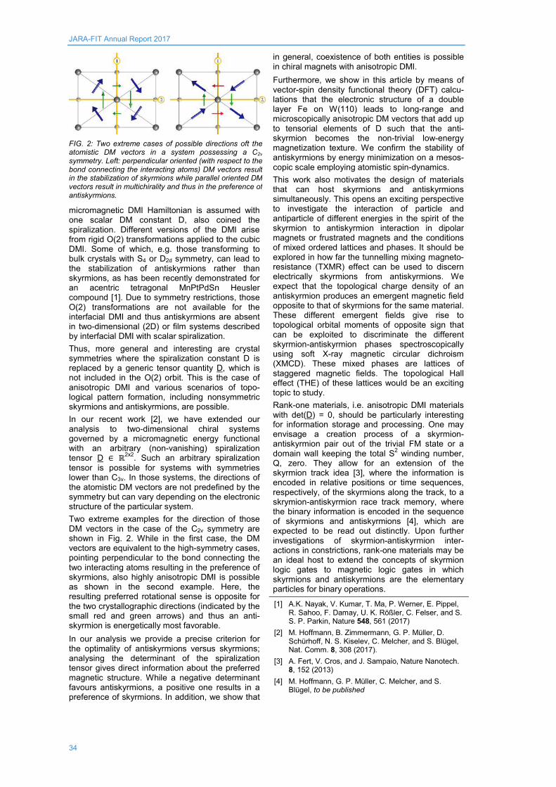
JARA-FIT Annual Report 2017
34
micromagnetic DMI Hamiltonian is assumed with one scalar DM constant D, also coined the spiralization. Different versions of the DMI arise from rigid O(2) transformations applied to the cubic DMI. Some of which, e.g. those transforming to bulk crystals with S4 or D2d symmetry, can lead to the stabilization of antiskyrmions rather than skyrmions, as has been recently demonstrated for an acentric tetragonal MnPtPdSn Heusler compound [1]. Due to symmetry restrictions, those O(2) transformations are not available for the interfacial DMI and thus antiskyrmions are absent in two-dimensional (2D) or film systems described by interfacial DMI with scalar spiralization. Thus, more general and interesting are crystal symmetries where the spiralization constant D is replaced by a generic tensor quantity D, which is not included in the O(2) orbit. This is the case of anisotropic DMI and various scenarios of topo-logical pattern formation, including nonsymmetric skyrmions and antiskyrmions, are possible. In our recent work [2], we have extended our analysis to two-dimensional chiral systems governed by a micromagnetic energy functional with an arbitrary (non-vanishing) spiralization tensor D ∈ ℝ2x2. Such an arbitrary spiralization tensor is possible for systems with symmetries lower than C3v. In those systems, the directions of the atomistic DM vectors are not predefined by the symmetry but can vary depending on the electronic structure of the particular system. Two extreme examples for the direction of those DM vectors in the case of the C2v symmetry are shown in Fig. 2. While in the first case, the DM vectors are equivalent to the high-symmetry cases, pointing perpendicular to the bond connecting the two interacting atoms resulting in the preference of skyrmions, also highly anisotropic DMI is possible as shown in the second example. Here, the resulting preferred rotational sense is opposite for the two crystallographic directions (indicated by the small red and green arrows) and thus an anti-skyrmion is energetically most favorable. In our analysis we provide a precise criterion for the optimality of antiskyrmions versus skyrmions; analysing the determinant of the spiralization tensor gives direct information about the preferred magnetic structure. While a negative determinant favours antiskyrmions, a positive one results in a preference of skyrmions. In addition, we show that
in general, coexistence of both entities is possible in chiral magnets with anisotropic DMI. Furthermore, we show in this article by means of vector-spin density functional theory (DFT) calcu-lations that the electronic structure of a double layer Fe on W(110) leads to long-range and microscopically anisotropic DM vectors that add up to tensorial elements of D such that the anti-skyrmion becomes the non-trivial low-energy magnetization texture. We confirm the stability of antiskyrmions by energy minimization on a mesos-copic scale employing atomistic spin-dynamics. This work also motivates the design of materials that can host skyrmions and antiskyrmions simultaneously. This opens an exciting perspective to investigate the interaction of particle and antiparticle of different energies in the spirit of the skyrmion to antiskyrmion interaction in dipolar magnets or frustrated magnets and the conditions of mixed ordered lattices and phases. It should be explored in how far the tunnelling mixing magneto-resistance (TXMR) effect can be used to discern electrically skyrmions from antiskyrmions. We expect that the topological charge density of an antiskyrmion produces an emergent magnetic field opposite to that of skyrmions for the same material. These different emergent fields give rise to topological orbital moments of opposite sign that can be exploited to discriminate the different skyrmion-antiskyrmion phases spectroscopically using soft X-ray magnetic circular dichroism (XMCD). These mixed phases are lattices of staggered magnetic fields. The topological Hall effect (THE) of these lattices would be an exciting topic to study. Rank-one materials, i.e. anisotropic DMI materials with det(D) = 0, should be particularly interesting for information storage and processing. One may envisage a creation process of a skyrmion-antiskyrmion pair out of the trivial FM state or a domain wall keeping the total S2 winding number, Q, zero. They allow for an extension of the skyrmion track idea [3], where the information is encoded in relative positions or time sequences, respectively, of the skyrmions along the track, to a skrymion-antiskyrmion race track memory, where the binary information is encoded in the sequence of skyrmions and antiskyrmions [4], which are expected to be read out distinctly. Upon further investigations of skyrmion-antiskyrmion inter-actions in constrictions, rank-one materials may be an ideal host to extend the concepts of skyrmion logic gates to magnetic logic gates in which skyrmions and antiskyrmions are the elementary particles for binary operations.
[1] A.K. Nayak, V. Kumar, T. Ma, P. Werner, E. Pippel, R. Sahoo, F. Damay, U. K. Rößler, C. Felser, and S. S. P. Parkin, Nature 548, 561 (2017)
[2] M. Hoffmann, B. Zimmermann, G. P. Müller, D. Schürhoff, N. S. Kiselev, C. Melcher, and S. Blügel, Nat. Comm. 8, 308 (2017).
[3] A. Fert, V. Cros, and J. Sampaio, Nature Nanotech. 8, 152 (2013)
[4] M. Hoffmann, G. P. Müller, C. Melcher, and S. Blügel, to be published
FIG. 2: Two extreme cases of possible directions oft the atomistic DM vectors in a system possessing a C2v symmetry. Left: perpendicular oriented (with respect to the bond connecting the interacting atoms) DM vectors result in the stabilization of skyrmions while parallel oriented DM vectors result in multichirality and thus in the preference of antiskyrmions.
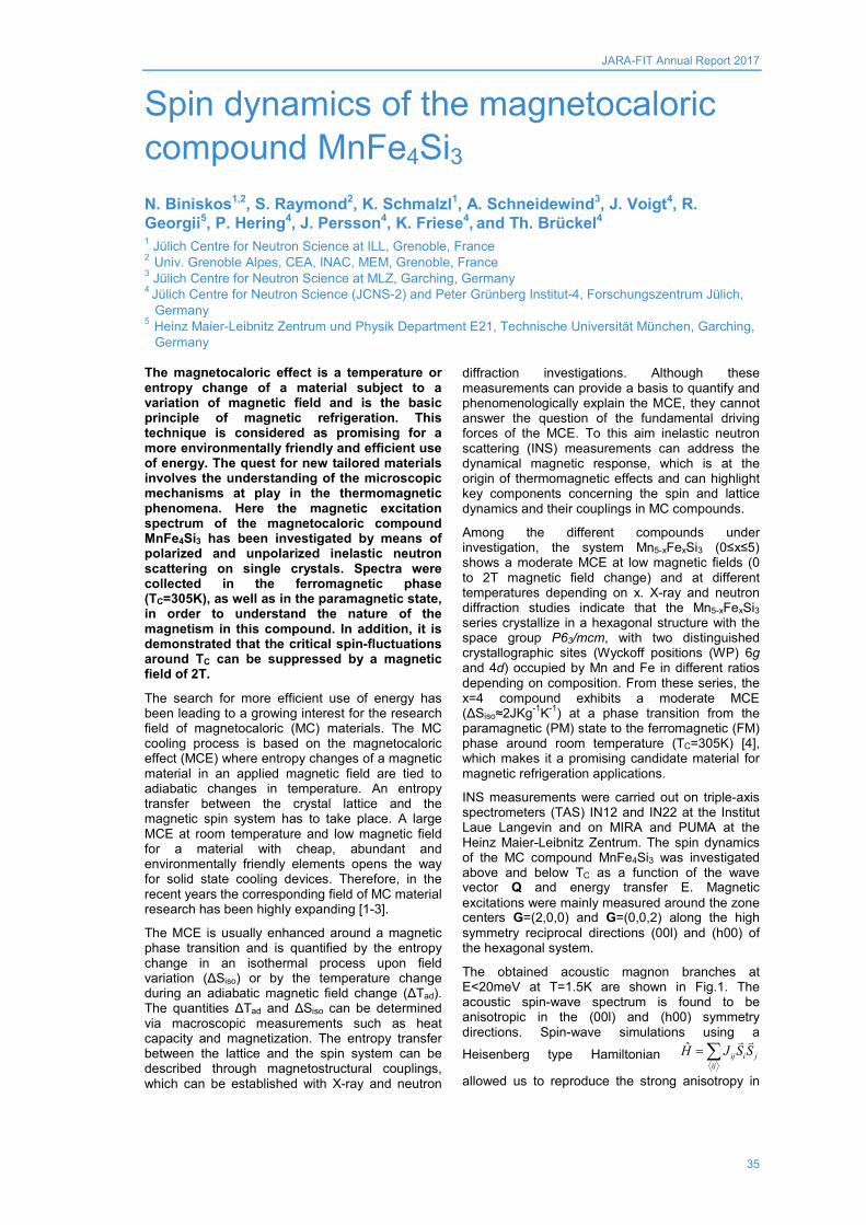
JARA-FIT Annual Report 2017
35
Spin dynamics of the magnetocaloric compound MnFe4Si3 N. Biniskos1,2, S. Raymond2, K. Schmalzl1, A. Schneidewind3, J. Voigt4, R. Georgii5, P. Hering4, J. Persson4, K. Friese4, and Th. Brückel4 1 Jülich Centre for Neutron Science at ILL, Grenoble, France 2 Univ. Grenoble Alpes, CEA, INAC, MEM, Grenoble, France 3 Jülich Centre for Neutron Science at MLZ, Garching, Germany 4 Jülich Centre for Neutron Science (JCNS-2) and Peter Grünberg Institut-4, Forschungszentrum Jülich,
Germany 5 Heinz Maier-Leibnitz Zentrum und Physik Department E21, Technische Universität München, Garching,
Germany The magnetocaloric effect is a temperature or entropy change of a material subject to a variation of magnetic field and is the basic principle of magnetic refrigeration. This technique is considered as promising for a more environmentally friendly and efficient use of energy. The quest for new tailored materials involves the understanding of the microscopic mechanisms at play in the thermomagnetic phenomena. Here the magnetic excitation spectrum of the magnetocaloric compound MnFe4Si3 has been investigated by means of polarized and unpolarized inelastic neutron scattering on single crystals. Spectra were collected in the ferromagnetic phase (TC=305K), as well as in the paramagnetic state, in order to understand the nature of the magnetism in this compound. In addition, it is demonstrated that the critical spin-fluctuations around TC can be suppressed by a magnetic field of 2T.
The search for more efficient use of energy has been leading to a growing interest for the research field of magnetocaloric (MC) materials. The MC cooling process is based on the magnetocaloric effect (MCE) where entropy changes of a magnetic material in an applied magnetic field are tied to adiabatic changes in temperature. An entropy transfer between the crystal lattice and the magnetic spin system has to take place. A large MCE at room temperature and low magnetic field for a material with cheap, abundant and environmentally friendly elements opens the way for solid state cooling devices. Therefore, in the recent years the corresponding field of MC material research has been highly expanding [1-3].
The MCE is usually enhanced around a magnetic phase transition and is quantified by the entropy change in an isothermal process upon field variation (ΔSiso) or by the temperature change during an adiabatic magnetic field change (ΔTad). The quantities ΔTad and ΔSiso can be determined via macroscopic measurements such as heat capacity and magnetization. The entropy transfer between the lattice and the spin system can be described through magnetostructural couplings, which can be established with X-ray and neutron
diffraction investigations. Although these measurements can provide a basis to quantify and phenomenologically explain the MCE, they cannot answer the question of the fundamental driving forces of the MCE. To this aim inelastic neutron scattering (INS) measurements can address the dynamical magnetic response, which is at the origin of thermomagnetic effects and can highlight key components concerning the spin and lattice dynamics and their couplings in MC compounds.
Among the different compounds under investigation, the system Mn5-xFexSi3 (0≤x≤5) shows a moderate MCE at low magnetic fields (0 to 2T magnetic field change) and at different temperatures depending on x. X-ray and neutron diffraction studies indicate that the Mn5-xFexSi3 series crystallize in a hexagonal structure with the space group P63/mcm, with two distinguished crystallographic sites (Wyckoff positions (WP) 6g and 4d) occupied by Mn and Fe in different ratios depending on composition. From these series, the x=4 compound exhibits a moderate MCE (ΔSiso≈2JKg-1K-1) at a phase transition from the paramagnetic (PM) state to the ferromagnetic (FM) phase around room temperature (TC=305K) [4], which makes it a promising candidate material for magnetic refrigeration applications.
INS measurements were carried out on triple-axis spectrometers (TAS) IN12 and IN22 at the Institut Laue Langevin and on MIRA and PUMA at the Heinz Maier-Leibnitz Zentrum. The spin dynamics of the MC compound MnFe4Si3 was investigated above and below TC as a function of the wave vector Q and energy transfer E. Magnetic excitations were mainly measured around the zone centers G=(2,0,0) and G=(0,0,2) along the high symmetry reciprocal directions (00l) and (h00) of the hexagonal system.
The obtained acoustic magnon branches at E<20meV at T=1.5K are shown in Fig.1. The acoustic spin-wave spectrum is found to be anisotropic in the (00l) and (h00) symmetry directions. Spin-wave simulations using a
Heisenberg type Hamiltonian ˆij i j
ijH J S S= ∑
allowed us to reproduce the strong anisotropy in

JARA-FIT Annual Report 2017
36
the two hexagonal directions and to extract the dominant in-plane (2SJ1=-4meV) and out-of-plane (2SJ2=-18meV) FM interactions of the system [5].
FIG. 1: Acoustic spin-waves of MnFe4Si3 at 1.5K along the (00l) and (h00) high symmetry hexagonal directions. Red lines correspond to spin-wave simulations.
To get insight into the spin dynamics above TC, the PM scattering was investigated at 1.036∙TC=316K. The obtained q-dependent susceptibility χq is shown in Fig.2. χq decreases faster along the (00l) direction compared to (h00), indicating a shorter inverse spin correlation length κq. A Lorentzian fit for χq gives the values 0.054(3)Å-1 and 0.14(1)Å-1 for κq along the (00l) and (h00) directions, respectively. The bare inverse spin correlation length κ0 for a Heisenberg model within the mean-field approximation can be calculated by
0C
C
TT T
κ κ=−
. The calculated values κ0 for the
(h00) and (00l) directions are 0.74(5) Å-1 and 0.284(16)Å-1, respectively. Comparing the corresponding spin correlation lenghts ξ0=κ0
-1 with the lattice parameters a and c, one can expect a localized feature of the magnetism of MnFe4Si3 [5].
FIG. 2: q-dependent susceptibility χq of MnFe4Si3 at 316K along the (00l) and (h00) high symmetry hexagonal directions. Red lines correspond to Lorentzian fits.
Short-range magnetic correlations in the PM state were also observed in Fe2P-based MC
compounds. However, their importance concerning the MCE is not clearly demonstrated. Therefore, we investigated the evolution of elastic scattering as a function of magnetic field near TC (see Fig.3) at the lowest accessible Q range with TAS. In this very low Q range, the contribution to the intensity in the spectra is mainly due to magnetic scattering. It is demonstrated that the critical scattering is suppressed by a magnetic field of 2T. To get insight into the observed behavior a comparison with a model that estimates the q-dependent susceptibility under a finite external magnetic field using the Landau theory for the magnetic fluctuations was employed [5]. The obtained calculation for the field-dependent susceptibility χq(H,TC) is shown in the inset of Fig.3 and describes qualitatively well the experimental data.
FIG. 3: Evolution of elastic scattering of MnFe4Si3 at 300K as a function of magnetic field. Dashed lines are guides for the eyes. The inset shows a calculation of the field dependence of χq(H,TC).
Here, we show with INS on MnFe4Si3 single crystals that: i) a strong anisotropy between the in- and out-of-plane magnetic exchange interactions is observed in the FM phase, ii) the spin correlation lengths measured in the PM state point to short-range order if compared to typical distances and iii) the critical fluctuations around TC can be suppressed by a magnetic field of 2T.
So far it is not clear which ingredient is favorable to produce a large MCE. Nonetheless, this study suggests that the strong response of the critical fluctuations in the PM state to a magnetic field of 2T is an important feature.
[1] O. Tegus et al., Nature 415, 150-152 (2002) [2] N. H. Dung et al., Adv. Energy Mater. 1, 1215
(2011) [3] X. Moya et al., Nature materials 13, 439 (2014) [4] Songlin et al., J. Alloys Compounds 334, 249
(2002) [5] N. Biniskos et al., Phys. Rev. B 96, 104407 (2017)

JARA-FIT Annual Report 2017
37
Spin Structure of MnO Nanoparticles, powder and single crystal X. Sun1, A. Klapper1, E. Feng2, Y. Su2, K. Nemkovski2, H. Bauer3, A. Schilmann3, O. Köhler3, W. Tremel3, O. Petracic1, and Th. Brückel1 1 Jülich Centre for Neutron Science (JCNS-2) and Peter Grünberg Institut-4, Forschungszentrum Jülich,
Germany 2 Jülich Centre for Neutron Science at MLZ, Garching, Germany 3 Institut für Anorganische Chemie und Analytische Chemie, Johannes Gutenberg-Universität Mainz,
Mainz, Germany
As one of the first studied materials using neutron scattering, MnO has been intensely investigated both in nanoparticle (NP) and bulk form. Despite numerous studies, its spin structure is still not well-understood. Zero field cooled (ZFC) magnetization measurements of MnO NPs show a low temperature peak at ~ 25 K instead of the expected feature at the Néel temperature of MnO. However, polarized neutron scattering shows the expected behavior of the antiferromagnetic (AF) order parameter vanishing around 118 K. We conclude that the magnetic behavior of MnO particles can be explained by a superposition of superparamagnetic (SPM)-like thermal fluctuations of the AF-Néel vector inside the AF core and a magnetic coupling to a ferrimagnetic (FiM) Mn2O3 or Mn3O4 shell. Interestingly, ZFC curves of MnO powder and a single crystal show also a peculiar peak at low temperatures similar to the low temperature peak observed in MnO NPs. However, these peaks originate from either a small amount of nanosized particles or FiM Mn2O3 or Mn3O4 impurities. Magnetic NPs have attracted considerable interest for decades both in fundamental research and industry. This is due to their potential applications in magnetic data storage, ferrofluidic systems and medicine [1-4]. With decreasing particle size, they may show novel magnetic, electronic and optical properties due to finite size or surface effects. In this report, we focus on MnO NPs, which is a text-book antiferromagnet (AF) with a bulk Néel temperature of 118 K. Above its TN, it is paramagnetic and has a rocksalt crystal structure [5].
Fig. 1 shows the ZFC/Field cooled (FC) magnetization curves of MnO NPs with 12 nm diameter compared to bulk samples (powder and single crystal). At about 25 K, a peak can be found in the ZFC curve of NPs (Fig. 1(a)). However, no feature indicating the Néel temperature at 118 K could be found. This is usually attributed to SPM behavior. However, the field dependence of the peak temperature shows only a weak decrease even up to 1 T (data not shown). Such weak field dependence is very different from that of SPM systems. There, the blocking temperature
decreases rapidly with an increasing magnetic field and disappears at a few hundred or thousand mT. A stability of this peak temperature is usually expected only for AF systems, because most AFs have a very high critical field.
FIG. 1: ZFC/FC magnetization curves of (a) 12nm MnO NPs, (b) MnO powder and (c) MnO single crystal measured at 100mT. Insets in panel (a) and (c) are enlarged views near the Néel temperature. (d) and (e) show the SEM images of MnO NPs with 12nm diameter and MnO powder, respectively. (f) shows a photo of one piece of the MnO single crystal.
To confirm the AF order of MnO NPs, polarized neutron scattering was performed using the DNS instrument at MLZ. As can be seen in Fig. 2(a), the magnetic component (red circles) could be successfully separated from the nuclear coherent (black squares) and spin-incoherent (blue triangles) components despite the extremely small amount of sample (50 mg), as well as the hydrogen contained in the oleic acid shell covering the particles. This could only have been achieved with the help of polarization analysis. By measuring the temperature dependence of the intensity of the magnetic (1
21212) Bragg peak, the
expected behavior of the AF order parameter that vanishes between 100 and 140 K can be observed, i.e. near the bulk TN = 118 K of MnO (Fig. 2(b)). The magnetic (1
21212) Bragg peak was
fitted with a pseudo-Voigt function.

JARA-FIT Annual Report 2017
38
FIG. 2: (a) Separated neutron-scattering contributions of 12 nm MnO NPs from polarized neutron scattering measured at 4 K. (b) Temperature dependence of the integrated intensity of the AF (1
21212) Bragg peak. The red
line is a guide to the eye assuming the bulk TN of 120 K and a continuous transition. The inset (i) in (b) shows the magnetic (1
21212) Bragg peaks at different temperatures.
The inset (ii) in (b) displays the magnetic correlation length as a function of temperature. (Reprinted figure with permission from [6] Copyright (2017) by the American Physical Society.)
The instrument resolution of DNS is considered as the width of the Gaussian profile, and the broadening due to the nano-size of the particles as the width of the Lorentzian profile. Using the Scherrer formula, the magnetic correlation lengths ξ of MnO can be obtained. In the inset of Fig. 2(b), a T vs ξ curve can be found. At low temperatures, the magnetic correlation length is about 6-7 nm for 12 nm NPs. This is possibly due to disordered surface spins, an AF domain state, or the presence of an oxidized Mn2O3 or Mn3O4 shell. As the temperature increases, the correlation length decreases due to thermal fluctuation.
Interestingly, a low temperature peak was also found in the ZFC magnetization curves of bulk MnO samples in addition to the expected feature indicating the PM-to-AF phase transition at TN (Fig.1(b) and (c)) [7]. Therefore, this peak might originate intrinsically from the frustrated superexchange interactions in MnO. For the powder sample, this peak shows similar behavior to that for the NPs. The AF order parameter shows no feature near this peak temperature in the polarized neutron scattering. It is likely, that this low temperature peak is due to the nano-sized particles between or attached to the large powder particles (Fig.1(e)). For the single crystal, the low temperature peak is relatively sharp compared to the one observed for NPs and powder and shows a greater resemblance to the behavior of a ferromagnet (FM) or ferrimagnet (FiM). Moreover, the temperature of 40K agrees roughly with the Curie temperature of Mn3O4 (42K). A decrease in the order parameter near the expected Q-value of
the (2 0 2) and (2 1 1) Bragg peaks of FiM Mn3O4 was found in the neutron scattering. However, no peak is observed below TN of MnO in single phase powder sample after an annealing procedure. We conclude that this peak originates from nanosized particles for powder samples or a small quantity of FiM Mn2O3 or Mn3O4 impurities at the interfaces between MnO crystal twins, respectively.
FIG. 3: Model to explain the magnetism in MnO NPs: the MnO core shows antiferro-SPM (AF-SPM) behavior while it is exchange coupled to a ferrimagnetic Mn2O3 or Mn3O4 shell.
Summarizing our findings, the magnetic behavior of MnO NPs can be explained by a superposition of superparamagnetic-like thermal fluctuations of the AF-Néel vector inside the AF core and a magnetic coupling to a ferromagnetic/FiM Mn2O3 or Mn3O4 shell as shown in Fig. 3. Above TN ≈ 118 K, the system is paramagnetic. Magnetometry result shows a Curie-Weiss behavior in the magnetization curve, and the neutron scattering shows no AF order. At a temperature between Tp and TN, the AF-Néel vectors inside the NPs fluctuate similar to a SPM system. This can be called an AF-SPM state. In this case, the AF order can be measured using neutron scattering, which has a probing time of ~ps. Magnetometry probes at a time scale of ~s. During this time, only a fluctuating AF order can be “seen”. Therefore, an average magnetization of zero is measured. Below Tp, both magnetometry and neutron scattering observe a “blocked” AF state. In neutron scattering, the AF order parameter continues increasing as the temperature decrease. In magnetometry, the crossover between the blocked and unblocked states is marked by a peak similar to a SPM. For bulk MnO, the low temperature peak found in the ZFC curves of MnO powder and single crystal samples are due to nanosized particles or partially oxidized Mn2O3 or Mn3O4 impurities, respectively.
[1] S. Sun, Adv. Mater. 18, 393 (2006) [2] M. Zahn, J. Nanoparticle Res. 3, 73 (2001) [3] S. Bedanta, A. Barman, W. Kleemann, O. Petracic,
and T. Seki, J. Nanomater. 2013, 1 (2013) [4] B. D. Terris and T. Thomson, J. Phys. D. Appl.
Phys. 38, R199 (2005) [5] C. G. Shull, W. A. Strauser, and E. O. Wollan,
Phys. Rev. 83, 333 (1951) [6] X. Sun, A. Klapper, Y. Su, K. Nemkovski, A.
Wildes, H. Bauer, O. Köhler, A. Schilmann, W. Tremel, O. Petracic, and T. Brückel, Phys. Rev. B 95, 134427 (2017)
[7] X. Sun, E. Feng, Y. Su, K. Nemkovski, O. Petracic, and T. Brückel, J. Phys. Conf. Ser. 862, 12027 (2017).
JARA-FIT Annual Report 2017
39
Magnetic excitations in the ground state of Yb2Ti2O7 V. Peçanha Antonio1,2, E. Feng1, Y. Su1, V. Pomjakushin3, F. Demmel4, L.-J. Chang5, R. Aldus1, Y. Xiao6, M. R. Lees7, and Th. Brückel6,1 1 Jülich Centre for Neutron Science (JCNS) at MLZ, Germany 2 Physik-Department, Technische Universität München, Germany 3 Laboratory for Neutron Scattering and Imaging (LNS), Paul Scherrer Institute, Switzerland 4 ISIS Facility, Rutherford Appleton Laboratory, United Kingdom 5 Department of Physics, National Cheng Kung University, Taiwan 6 Jülich Centre for Neutron Science (JCNS-2) and Peter Grünberg Institut-4, Forschungszentrum Jülich,
Germany 7 Department of Physics, University of Warwick, United Kingdom Frustrated magnets constitute a sui-generis class of magnetic materials. Due to their exotic excitations, they are of interest for the development of future quantum technologies. The frustration, which arises as a direct consequence of the lattice geometry, is the mechanism that, in theory, may inhibit long-range order at temperatures as low as absolute zero. The pyrochlore family of compounds is the most studied class of frustrated magnets in three dimensions. Paradoxically, pyrochlores are mainly interesting due to their magnetic ground states, which in general, and despite the frustration, are magnetically ordered. In this work, we study a prominent member of the pyrochlore family: the titanate Yb2Ti2O7. Until recently, it was believed that Yb2Ti2O7 evaded long-range order. We show that the compound does order around 280 mK, where a sharp cusp in the heat capacity is observed. Moreover, we present high-resolution neutron inelastic data at zero magnetic field that shows the magnetic excitations in Yb2Ti2O7 with unprecedented details for a powder sample of the compound.
A system is said to be frustrated when the energies of all competing interactions cannot be simultaneously minimized. The compounds of chemical formula A2B2O7, where A is a rare earth and B is a transition metal, known as pyrochlores, represent an important class of frustrated materials. Their crystallographic lattice of corner-sharing tetrahedra, forming in the cubic Fd-3m crystallographic space group, is an essential requirement for the material to present geometrical frustration. Pyrochlore compounds are expected to host many exotic phases of matter. One of the most celebrated is the classical spin-ice phase: spin-ice compounds present a frozen glassy two-in-two-out short range magnetic structure, where, due to strong Ising single-ion anisotropy, two magnetic moments point to the centre of one tetrahedra motif and two point out. Beyond the spin-ice state, pyrochlores present an extensive roster of magnetic structures at very low temperatures, from antiferromagnetic-XY to collinear ferromagnetic states.
The latter is the case of the compound we present here. Yb2Ti2O7 has been for many years an elusive puzzle in the pyrochlore titanate series. Many characteristics of this compound were misunderstood, mainly because the low temperature magnetic behaviour of ytterbium titanate is strongly sensitive to the sample quality. By quality we mean not only phase formation and crystallinity, but also stoichiometry. For this reason, probing the sample precise composition becomes an indispensable prerequisite and, being so, it was the first step performed in this work. By means of Rietveld refinements of neutron diffraction data, we show that our sample can be regarded as a very good exemplar of Yb2Ti2O7, with a small deviation in the stoichiometry (at most 1% of B sites are occupied by Yb3+ ions).
Following sample characterization, we also checked the heat capacity anomaly displayed by our sample. To determine the heat capacity anomaly temperature and sharpness has been shown to be one of the most efficient methods to also determine the sample quality. Non-stoichiometric single-crystalline samples usually display broader anomalies at variable temperature ranges. Powders, on the other hand, display the anomaly between 260 and 280 mK. The heat capacity anomaly measured on our sample, at zero and small magnetic fields, is shown in FIG. 1. The shift of the anomaly to higher temperatures, as well as the broadening of the peak with increasing field, are a good indicative that the sample indeed undergoes a ferromagnetic phase transition at 280 mK. Neutron diffraction measurements at low temperatures were carried out on the same sample at the instruments DNS, at MLZ in Germany, and OSIRIS, at ISIS in United Kingdom. Both results are consistent with the development of an essentially collinear ferromagnetic structure, with spins pointing along the equivalent [100] cubic axes. This structure, curiously, is unique in the whole pyrochlore family, in which another sister compounds with different A and B sites are included. Due to the single ion anisotropy, usually the ordered magnetic moments point either along the Z-axis, i.e. the [111] direction or the line that

JARA-FIT Annual Report 2017
40
connects the centres of two adjacent tetrahedra, or along the plane perpendicular to it, forming the class of XY pyrochlores. We show also in Fig. 1 the diffraction pattern obtained at OSIRIS. With considerable better resolution, we can estimate a correlation length of at least ~ 800 Å, which means that the ferromagnetic structure is genuinely long-ranged.
FIG. 1: On the left, heat capacity measured at zero and several small magnetic fields. The sharp anomaly broadens and shifts to higher temperatures, characteristic of a ferromagnetic phase transition. On the right, diffraction patterns measured at DNS (top panel) and OSIRIS (bottom). Note the different momentum transfer scale. The magnetic structure can be regarded as a collinear ferromagnet, which is depicted in the left bottom. Based on the resolution of OSIRIS, we calculate a correlation length of 800 Å of the magnetic structure at 50 mK.
Additional information about the magnetism at low temperatures in Yb2Ti2O7 can be obtained using high-resolution inelastic neutron scattering. We show in Fig. 2 the colour contour plots of the spectra measured at different temperatures.
FIG. 2: Color contour plots of the spectra measured for Yb2Ti2O7 at (a) 10 K, (b) 2.5 K, (c) 500 mK and (d) 50 mK.
Intentionally, we display here four spectra that represent specific temperature intervals where different magnetic correlations are manifested. At 10 K, the sample behaves as a classical paramagnet and few inelastic signal is observed. At 2.5 K, an intensity increase in the low energy, low momentum transfer |Q| region of the spectra can be seen. It develops further with decreasing temperature, appearing considerably stronger at 500 mK. Another interesting feature, also clear at 500 mK, is some higher energy, broad, diffuse
scattering. It corresponds to the so-called continuum of scattering in Yb2Ti2O7, and the reason for its presence is still uncertain. However, it is clear that the continuum develops already much above the sharp phase transition temperature [see Fig. 3 panels (g)-(h)]. The most obvious difference between the spectrum at 500 mK and the one at 50 mK is the gap that opens at low-|Q|. This strong branch, around 0.2 meV is the single reminiscent of conventional spin-wave excitations in the apparent conventional ferromagnetic state of this compound.
FIG. 3: Representative cuts performed along energy [(a)-(g)] and |Q| axis. The intervals in energy and momentum transfer were chosen to highlight important features measured on the Yb2Ti2O7 spectra.
In Fig. 3, we display some representative cuts along the energy axis [panels (a)-(g)]. From panels (a)-(c) we show the evolution of the paramagnetic fluctuations (green shaded area) with decreasing temperature at low-|Q|. The narrowing of the line shape at the neutron energy gain side (i.e. negative energy side) is consequence of the Principle of Detailed Balance. In panels (d)-(f), we show several cuts, performed at different momentum transfer intervals, at 50 mK. Those figures display clearly all the excitations present at low temperature in our Yb2Ti2O7 sample. The most evident is the strong gapped excitation at low-|Q| (red dashed area). Also evident at higher momentum transfers is a second sharp mode at 0.1 meV and the broad continuum (blue dashed area). Underneath all the aforementioned excitations, at the lowest temperature measured a remnant paramagnetic scattering survives deep in the ordered phase.
In conclusion, basically all the dynamics measured in our Yb2Ti2O7 sample, including the persistent paramagnetic scattering at a temperature as low as 50 mK, are exotic and, ultimately, also unique in Yb2Ti2O7. Our work points out the complicated physics encoded in frustrated magnets. The unconventional coexistence of long-range order with persistent paramagnetic fluctuations and a continuum of scattering constitutes a still unsolved, challenging puzzle in modern condensed matter physics.
[1] V. Peçanha-Antonio, E. Feng, Y. Su, V. Pomjakushin, F. Demmel, L.-J. Chang, R. J. Aldus, Y. Xiao, M. R. Lees, and T. Brückel, Phys. Rev. B 96, 214415 (2017).

JARA-FIT Annual Report 2017
41
Strain and electric-field control of magnetism in supercrystalline iron oxide nanoparticle–BaTiO3 composites L.-M. Wang1, O. Petracic1, E. Kentzinger1, U. Rücker1, M. Schmitz1, X.-K. Wei2, M. Heggen2, and Th. Brückel1 1 Jülich Centre for Neutron Science (JCNS-2) and Peter Grünberg Institut-4, Forschungszentrum Jülich,
Germany. 2 Ernst Ruska-Centre for Microscopy and Spectroscopy with Electrons and Peter Grünberg Institute-5, Forschungszentrum Jülich, Germany Magnetoelectric (ME) materials are promising candidates for electric field controlled memory elements. The ability of a purely electric manipulation of the magnetization offers the opportunity to design energy efficient magnetoelectric random access memories (MERAMs) [1]. We reported the manipulation of the magnetism of self-assembled iron oxide nanoparticle (NP) monolayers on top of BaTiO3 (BTO) single crystal. Strain induced magnetoelectric coupling (MEC) is observed. Cross-sectional scanning transmission electron microscopy (STEM) provide information about the layer structure of the sample. This work opens up viable possibilities for fabricating novel electronic devices by self-assembly techniques.
Magnetoelectric (ME) materials are systems where a magnetic field can manipulate the polarization or an electric field the magnetization. They have stimulated great research interest due to their potential applications in spintronics or multifunctional devices. Moreover, the possibility to switch the magnetization via an electric field could reduce the energy consumption to write data in electronic devices and offers the possibility to scale down magnetic random access memories (MRAMs) further.
However, ME systems based on nanoparticles (NPs) are very limited. NPs can be considered as building blocks for artificial super-structures. One prominent route is to employ the self-organization of NPs into regular arrangements, so called “supercrystalline lattices” or “supercrystals”. Such systems are particularly interesting because of their prospective applications as multifunctional materials. Ferromagnetic (FM) – ferrolelectric (FE) or ferrimagnetic (FiM)–FE composites based on magnetic NPs are promising novel candidates for artificial nanoscale multiferroic devices. However, there are several open questions, e.g. what is the exact mechanism of MEC in such nanocomposites? How can it be tuned and optimized? Therefore, we investigated strain and electric field mediated magnetoelectric coupling (MEC) in a model system composed of a monolayer of self-assembled iron oxide NPs coupled to a BTO substrate.
Structural characterization of the NP ordering was also performed using SEM as displayed in Fig. 1(a) for the uncoated system. Fig. 1(b and c) show the results of different sample processing steps, i.e. after oxygen plasma etching to remove the oleic acid shells (Fig. 1b) with the 8 nm Ti layer between the substrate and NPs, and after coating the NPs with a 25 nm Au layer (Fig. 1c). The Au coating almost covers perfectly the NP layer as a percolated Au network embedding the NPs. This is evidenced by our STEM/EDX observation.
FIG. 1: (a) Zoomed-in on-top view of the BTO/NP sample observed by SEM. (b) A similar sample but with an 8 nm Ti layer deposited before spincoating the NPs. Moreover, the sample was treated in oxygen plasma (sample BTO/Ti/NP). (c) The same sample after deposition of a 25 nm Au capping layer on top of the NPs (sample BTO/Ti/NP/Au). (d–i) Z-Contrast high-angle annular-dark-field STEM image showing the stacking sequence of different layers in the BTO/Ti/NP/Au sample and the simultaneously collected EDX maps of Fe (blue), Au (pink), O (yellow), Ti (green) and Ba (red), respectively.
Fig. 1(d) shows the morphology of the multilayer system viewed along the cross-sectional direction. The upper white area represents hereby the Au layer. The elemental maps (Fig. 1(e–i)) detected by EDX clearly identify the Au/NP, NP/Ti and Ti/BTO interfaces, in which the BTO/Ti and Ti/NP interfaces are further manifested by the dark-contrast that the top surface of the Ti layer is oxidized while the bottom surface is oxygen-free, i.e. the dark band at the Ti/BTO interface indicating a pure metallic Ti layer. In addition, the coverage of the Au layer of about half of the particle diameter is revealed from the Fe and Au maps, see Fig. 1(e and f). For these three sample structures we measured the magnetic moment as a function of temperature for (a) the untreated NP

JARA-FIT Annual Report 2017
42
monolayer on top of the BTO substrate (BTO/NP), (b) the oxygen plasma treated NP monolayer deposited onto a Ti buffered BTO substrate (BTO/Ti/NP), and (c) the complete system, where the NPs are embedded in an Au top layer (BTO/Ti/NP/Au). The comparison of the data from the three systems yields several interesting observations. For the sample BTO/NP, the FC and FW curves are basically identical to each other and only a slight kink at the R–O phase transition at 190 K can be seen (Fig. 2a). No MEC is expected here. We attribute this kink to the magnetic response of the dipolarly coupled NPs to a change of the BTO corrugation and hence to the slight positional rearrangement of the NPs.
FIG. 2: (a–c) In-plane magnetic moment vs. temperature during field warming (FW) and during subsequent field cooling (FC) in 5 mT for the three types of samples, (a) BTO/NP, (b) BTO/Ti/NP and (c) BTO/Ti/NP/Au as depicted schematically in the insets. (d) Out-of-plane magnetic moment under the same conditions to be compared to (c). The vertical grey bars indicate the temperature region, where bulk BTO has first order phase transitions from tetragonal (T) to orthorhombic (O) to rhombohedral (R).
For the sample BTO/Ti/NP, the FC and FW curves show magnetization steps near the R–O transition at 190 K and the O–T transition at 287 K (Fig. 2b). We assume that strain mediated MEC is responsible for the observed magnetization changes. The results obtained on the BTO/Ti/NP/Au sample also display magnetization jumps but with a significantly enhanced amplitude as shown in Fig. 2(c). Our interpretation is that the embedding Au layer effectively mediates the strain produced by the BTO substrate onto the NPs and hence increases the MEC between BTO and NPs. Second, one should note the sign of the magnetization changes and the relative amplitudes at the phase transition temperatures. The FC curve hereby displays an about three times larger jump compared to the FW curve. At the T–O transition at around 280 K the FC curve shows a negative magnetization step, whereas FW is basically unaffected.
We demonstrate that the magnetization of the Au/BTO/Ti/NP/Au system (with a thin BTO substrate) can be influenced by DC and AC electric fields. Fig. 3(a) shows the magnetic
moment as a function of the applied DC electric field at room temperature. A typical butterfly shaped curve was obtained as expected from in-plane strain mediated MEC in ME composites.
FIG. 3:(a) Magnetic moment vs. applied electric field of the sample Au/BTO/Ti/ NP/Au at 300 K and 5 mT. The black data points were measured with increasing DC field from −20 to +20 kV cm-1, the red data points were measured in the reversed sequence (b) ME coefficient αME vs. temp. measured in an AC electric field with
f = 1 Hz, Emax = 3.2 kV cm-1 and a constant magnetic field of 5 mT.
Clearer evidence of a true MEC in contrast to possible artifacts is provided by probing the converse ME effect using magnetoelectric ac susceptibility (MEACS). The MEACS coefficient, αME, as a function of temperature is displayed in Fig. 3(b). The same sample as above, Au/BTO/Ti/NP/Au, was measured upon cooling using a frequency of 1 Hz and an AC electric field amplitude of 3.2 kV cm−1. The frequency and amplitude are chosen in such a way that the largest signal is observed while the electric field amplitude still probes the linear response regime which can be seen in Fig. 5(a). The curve shows two clear jumps in the BTO phase transition regions at 190 K and 280 K. Deep inside each phase the MEACS signal, being a direct probe of the MEC strength, is approximately constant. This is expected because inside a phase only a negligible change of strain occurs by lattice expansion. However, near the BTO phase transitions a large change of the MEC and hence a jump in the MEACS signal is observed due to the step-like transformation of the BTO lattice parameters, the change in the domain structure and consequently the change in the BTO surface morphology.
In conclusion, an efficient MEC effect with a large ME coefficient, between a supercrystalline monolayer of iron oxide NPs and a BTO substrate was demonstrated. The mechanism of the MEC effect can be understood as strain mediated coupling. The figures are reproduced from [3] with permission from the Royal Society of Chemistry.
[1] Barthélémy A, Bibes M., Nature Materials 7, 425 (2008)
[2] H. K. D. Kim, L. T. Schelhas, S. Keller, J. L. Hockel, S. H. Tolbert and G. P. Carman, Nano Letter 13, 884 (2013).
[3] L.-M. Wang, O. Petracic, E. Kentzinger, U. Rücker, M. Schmitz, X.-K. Wei, M. Heggen, Th. Brückel, Nanoscale 9, 35 (2017).

JARA-FIT Annual Report 2017
43
Atomic resolution imaging of YAlO3: Ce in the chromatic and spherical aberration corrected PICO electron microscope L. Jin1, J. Barthel1,2, C.L. Jia1,3, and K.W. Urban1,3 1 Ernst Ruska-Centre for Microscopy and Spectroscopy with Electrons, Forschungszentrum Jülich,
Germany 2 Gemeinschaftslabor für Elektronenmikroskopie, RWTH Aachen University, Germany 3 School of Electronic and Information Engineering and State Key Laboratory for Mechanical Behaviour of
Materials, Xi’an Jiaotong University, China The application of combined chromatic and spherical aberration correction in high-resolution transmission electron microscopy enables a significant improvement of the spatial resolution down to 50 pm. We demonstrate that such a resolution can be achieved in practice at 200 kV. The Y-Y-atom pairs in [010] projected yttrium orthoaluminate are successfully imaged together with the Al and the O atomic columns. Although the 57 pm pair separation is well demonstrated, separations between 55 pm and 80 pm are measured. This observation is tentatively attributed to structural relaxations and surface reconstruction in the very thin samples used. Quantification of the resolution limiting effective image spread is achieved based on an absolute match between experimental and simulated image intensity distributions, suggesting an instrumental resolution of 52 pm for the present experiment.
In a spherical aberration (CS) and chromatic aberration (CC) corrected electron microscope, the two major resolution limitations of previous instrument generations due to partial spatial and partial temporal coherence are significantly reduced. The spatial resolution of such an instrument is limited by an incoherent image spread which dampens linear and non-linear contributions at the same image frequency by an equal amount. This is an essential qualitative difference compared to the previously dominating partial temporal coherence effects, which in general cause a different dampening of linear and non-linear contributions. Besides, the typical sources of image spread, such as mechanical vibrations of the specimen holder and electrical instabilities of beam deflectors, thermal magnetic field-noise, also known as Johnson noise, is currently considered as the major contribution to the image spread in the C-COR setup. The C-COR allows unwanted coherent axial aberrations of the imaging system to be reduced effectively up to the fourth order (C4), leading to optimum phase-contrast transfer up to the information limit by
adjusting also the fifth-order spherical aberration (C5). The PICO microscope is equipped with an advanced version, C-COR+, of the image corrector. It is optimized for an as low as possible level of Johnson noise thus providing an improved resolution compared to that of C-COR at 200 kV.
In order to allow a comparison of the performance of different instruments, resolution has inevitably to be defined universally and independent of sample parameters. In reality, however, these parameters may be decisive for the direct perception of resolution in practical work. On the other hand, today, where information limits in the range of 50 pm are characterizing transmission electron microscopy (TEM), the dilemma of an insufficient image-signal separation due to sample parameters applies quite frequently and contrast simulations have become compulsory for image interpretation. These calculations are providing also an indirect access to the value of a microscope’s spatial resolution. However, a necessary condition in order to be able to extract the instrument resolution based on image simulations is a quantitative comparison of experimental intensities with calculated values on the same absolute scale. This has just recently been achieved. Within this numerical forward modeling of the imaging process in TEM the real atomic separation in the sample can be determined irrespective of whether this is directly visible in the images.
Here, we report on imaging b-axis oriented orthorhombic Ce-doped yttrium orthoaluminate (also known as yttrium-aluminium perovskite, YAP) with the Jülich PICO microscope operated at an acceleration voltage of 200 kV in TEM mode. We present details of the imaging experiments illustrating the performance of an instrument at the limit of what can be optically achieved today.
Our TEM images were taken employing the negative CS imaging (NCSI) technique on a 4k × 4k Gatan Ultrascan 4000 UHS camera at a sampling rate of 4.3 pm/pixel. Optimum contrast transfer for NCSI conditions considering third-order (C3) spherical aberration and C5 was treated.

JARA-FIT Annual Report 2017
44
Negative phase contrast, providing bright image contrast at atomic positions against a dark background, is obtained over a certain range of sample thicknesses for a negative value of C3 combined with a positive value of C5 and a positive defocus value C1 (overfocus).
FIG. 1:. Schematic view of 2×2×2 orthorhombic unit cells along the crystallographic b = [010] zone axis of YAP. The 57 pm Y-Y-atom pair separation is indicated. For the close O-Al-pairs the separation is 45 pm.
The YAP has the orthorhombic Pnma structure with lattice parameters a = 0.5330 nm, b = 0.7375 nm and c = 0.5180 nm [1]. Fig. 1 shows schematically the projection of 2×2×2 unit cells of the structure along the crystallographic b = [010] zone axis. Both the Y-Y-atom pairs and the O-Al-O atom arrangement occur in two different orientations, where the latter is due to opposing rotations of corner-sharing oxygen octahedra as indicated by the circular arrows. Our simulated HRTEM images along this axis evidenced that there is a range of defocus and thicknesses values that allow the separation of the close Y-Y-atom pairs to be directly imaged.
Fig. 2(a) displays an experimental image. The schematic in the upper left corner depicts the projection according to Fig. 1. In this original unfiltered image, both the Y-Y-atom pair and the oxygen atoms are resolved with rather high contrast. Also the two different orientations of the projected O-Al-O arrangement are clearly visible. Frequently one of the two Y-atom columns forming a pair shows stronger contrast compared to the other. As confirmed by contrast simulations this indicates a difference of ±1 atom in length of the two columns. Individual Y-atom pair separations were measured by locally fitting two Gaussian functions to the image intensity distribution. The apparent pair distances vary between 55 pm and 80 pm with a mean value of 69 pm and a standard deviation of 8 pm, c.f. Fig. 2(b). We note that the 57 pm atom pair separation is clearly resolved for both pair orientations as shown in Fig. 2(a) and (c). The substantial deviation from the bulk structure is attributed to lattice relaxation in the thin sample (1.7 nm) used.
Quantification of the resolution limiting effective image spread is achieved by iteratively matching the experimental image with simulations at an absolute contrast level. From this contrast transfer
limitation, we deduce an instrumental resolution of 52 pm for the present experiment.
FIG. 2:. (a) Experimental image along the b = [010] axis (unfiltered original). The schematic in the upper left corner depicts the projection according to Fig. 1 (projected oxygen octahedra indicated by blue lines). The Y-Y-atom pairs, the O-Al-O atom arrangement and the isolated O atoms are resolved. (b) Distribution of atom-pair separations in the image determined from Gaussian fits, where sd denotes the standard deviation of the data. (c) Example line profiles through Y-Y-atom pairs as marked yellow in (a) including the fitted Gaussian functions (red curves) and their sum (black curve), which demonstrate the resolution of a 68 pm and a 57 pm separation.
Finally, we would like to acknowledge an earlier brief report on YAlO3:Ce imaging by high-angle annular dark-field scanning TEM (STEM) [2]. Coherent TEM and incoherent STEM with 200 keV electrons show here comparable resolving power, as the close Y-Y separation can be directly observed in images obtained by either technique. However, in contrast to STEM, imaging by NCSI TEM shows also the oxygen atoms.
In conclusion, by application of combined CC and CS correction, the spatial resolution of transmission electron microscopes is significantly improved. This is demonstrated here by resolving the Y-Y-atom pairs in b-axis oriented YAlO3:Ce with a nominal separation of 57 pm in images recorded at 200 kV with the Jülich CC and CS corrected PICO microscope. To the best of our knowledge, this demonstrates the highest direct resolution in coherent TEM atomic imaging in materials at 200 kV to date [3].
[1] N.L. Ross, J. Zhao, and R.J. Angle, J. Solid State Chem. 177, 1276 (2004)
[2] T. Kishida, M. Koschan, M. zhuravleva, C.L. Melcher, G. Duscher, and M.F. Chisholm, Microsc. Microanal. 20 (suppl 3), 132 (2014)
[3] L. Jin, J. Barthel, C.L. Jia, and K.W. Urban, Ultramicroscopy 176, 99 (2017)

JARA-FIT Annual Report 2017
45
[NiAs]-type polymorph of FeN W. P. Clark1, S. Steinberg2, R. Dronskowski2, C. McCammon3, I. Kupenko4, M. Bykov3, L. Dubrovinsky3, L. G. Akselrud5, U. Schwarz5, and R. Niewa1
1 Institute of Inorganic Chemistry, University of Stuttgart, Germany 2 Institute of Inorganic Chemistry, RWTH Aachen University, Germany 3 Bayerisches Geoinstitut, University of Bayreuth, Germany 4 European Synchrotron Radiation Facility (ESRF), Grenoble, France 5 Max Planck Institute for Chemical Physics of Solids, Dresden, Germany Explorations of the high-pressure, high-temperature regimes for the economically relevant Fe−N system led to the discovery of an unprecedented form of FeN crystallizing with the nickel arsenide type of structure. In addition to the crystal structure, the magnetic properties and electronic structure of the new [NiAs]-type FeN were determined.
Determining the components and the physical properties of the iron−nitrogen system has attracted an enormous attention among materials scientists [1]. This quest was triggered by the ability of certain iron nitrides to serve as coatings for steel-based materials and as feasible magnetic recording media [1]. To date, examinations of the components for this system have solely resulted in the iron-rich nitrides Fe16N2, Fe8N, Fe4N, Fe3N, Fe2N, besides FeN [1]. To gain access to the nitrogen-rich components of this very system, explorations employing high temperatures and pressures have been conducted. In the course of these investigations, an unprecedented modification of equiatomic FeN has been discovered [2].
FIG. 1: Representations of the coordination polyhedra in the crystal structure of the [NiAs]-type polymorph of FeN: the nitrogen atoms (green) are surrounded by trigonal iron prisms, while the iron atoms (gray) reside in the centers of nitrogen octahedra. Reprinted with permission from reference [2].
Previous investigations on the equiatomic FeN proposed two different structure models based on the zinc-blende type and the rock-salt type for FeN [3]. The new form of FeN crystallizes with the
[NiAs] structure type (P63/mmc; at p = 0.0001 GPa; a = 2.80 Å; c = 5.02 Å; V = 34.05 Å3; Fig. 1) and was obtained from high-pressure and -temperature reactions. In particular, the [NiAs]-type of FeN was yielded from reactions of 57Fe or 57Fe2N with nitrogen which was utilized as both pressure medium and reactant at pressures ≥ 10 GPa and temperatures of 1300 K. The crystal structure of the nitride was determined based on Rietveld refinements of powder X-ray diffraction patterns that were collected using synchrotron radiation. Furthermore, the magnetic properties of the reactants and the diverse products were monitored by means of synchrotron source Mößbauer spectroscopy experiments.
FIG. 2: Mößbauer spectra at different pressures prior to as well as after laser heating. Black: 57Fe reactant in nitrogen medium at 5.3 GPa prior to laser heating; Red: formation of 57Fe2N/57Fe3N1+x after laser heating at 5.3 GPa; Green: multiplet of [NiAs]-type 57FeN after laser heating; Blue: Reformation of 57Fe2N/57Fe3N1+x after laser heating at pressures ≤ 10 GPa. Reprinted with permission from reference [2].
An inspection of the Mößbauer spectra (Fig. 2) revealed that an iron nitride with a composition close to Fe2N/Fe3N1.4 is obtained for temperatures up to 1300 K and pressures ≤ 10 GPa, while a magnetic sextet corresponding to the [NiAs]-type FeN is observed after annealing at temperatures ≥ 1300 K and pressures ≥ 10 GPa. This magnetic hyperfine splitting indicates a magnetic ground state for the [NiAs]-type FeN. Notably, additional laser heating of the [NiAs]-type FeN results in a transformation of FeN into Fe2N/Fe3N1.4 at a pressure ≤ 10 GPa. The crystal structure of the new FeN is composed of hexagonal close-packed layers of nitrogen atoms with iron atoms residing in all octahedral voids for the equiatomic composition (Figure 1).

JARA-FIT Annual Report 2017
46
FIG. 3: a) Energy−volume curves and b) pressure-dependent enthalpies of the [ZnS]-type and [NiAs]-type FeN; c) and d): non-spin-polarized DOS and –pCOHP curves of the [NiAs]-type FeN; e) and f): spin-polarized DOS and –pCOHP curves of the [NiAs]-type FeN. Reprinted with permission from reference [2].
More specifically, the nitrogen atoms reside in trigonal prisms assembled by the iron atoms, while the iron atoms are surrounded by nitrogen octahedra sharing common faces along the c axis.
Previous research on the electronic structures of the zinc blende type and rock salt type FeN showed that the former type of structure should be preferred [4]. A comparison of the energy-volume curves and pressure-dependent enthalpies for the zinc blende type and [NiAs]-type FeN (Figure 3) indicates that the zinc blende type is more favorable for the equiatomic iron nitride. To identify the reasons for this structural preference at the atomic scale, we followed up with an analysis of the electronic structure for the new polymorph of FeN.
The features at the Fermi level, EF, in the non-spin-polarized densities-of-states (DOS) and projected crystal orbital Hamilton population (pCOHP) curves clearly point to an electronically unfavorable situation for the [NiAs]-type FeN (Figure 3). In particular, the electronically unfavorable situation which is denoted by the position of EF at a maximum of the DOS and antibonding Fe−N interactions may be alleviated by approaching a magnetic state [5]. Indeed, the Fermi level falls in a pseudogap of the spin-polarized DOS of [NiAs]-type FeN – a typical fingerprint hinting to a ferromagnetic instability [5]. This outcome agrees well with experimentally determined magnetic
hyperfine splitting of [NiAs]-type FeN (Figure 2). A comparison of the integrated values of the projected COHP curves (IpCOHP) of [NiAs]-type FeN to those of the zinc blende type FeN [2] reveals that the latter form comprises shorter Fe−N contacts providing larger −IpCOHP values relative to those in the [NiAs]-type FeN. Thus, it can be inferred that the tendency to adopt the zinc blende type stems from the attempt to maximize the overall bonding at the atomic scale.
This work was supported by the Fonds der Chemischen Industrie e.V. through a Liebig-Stipend to S.S.. Furthermore, we wish to thank R. Rüffer and the staff members of the European Synchrotron Radiation Facility for the support regarding the use of the beamline ID18 (project no. CH-4383).
[1] S. Bhattacharyya, J. Phys. Chem. C 119, 1601, (2015)
[2] W. P. Clark, S. Steinberg, R. Dronskowski, C. McCammon, I. Kupenko, M. Bykov, L. Dubrovinsky, L. G. Akselrud, U. Schwarz, and R. Niewa, Angew. Chem. Int. Ed. 56, 7302, (2017)
[3] H. Nakagawa, S. Nasu, H. Fujii, M. Takahashi, and F. Kanamaru, Hyperfine Interact. 69, 455, (1991)
[4] B. Eck, R. Dronskowski, M. Takahashi, and S. Kikkawa, J. Mater. Chem. 9, 1527, (1999)
[5] G. A. Landrum and R. Dronskowski, Angew. Chem. Int. Ed. 39, 1560, (2000)

JARA-FIT Annual Report 2017
47
POWTEX and multi-dimensional Rietveld refinement of neutron time-of-flight powder diffraction P. Jacobs1, A. Houben1, W. Schweika2,3, A. L. Tchougréeff1, and R. Dronskowski1 1 Institute of Inorganic Chemistry, RWTH Aachen University, Germany 2 European Spallation Source ESS, Lund, Sweden 3 Jülich Center for Neutron Science (JCNS) and Peter Grünberg Institute-4, Germany POWTEX is an instrumentation project for time-of-flight neutron powder-diffraction and texture studies at the research reactor FRM II. The instrument components, e.g., the tailor-made, innovative 10B-detector system, have been designed, significantly advanced, manufactured and tested. Concurrently, the development of a multi-dimensional Rietveld refinement method has been worked out to fully exploit the possibilities of the new instrument concepts.
POWTEX (see Figure 1) is a time-of-flight (TOF) neutron powder-diffractometer awaiting on-site construction and commissioning phase at MLZ/FRM II. Funded by Germany’s Federal Ministry of Education and Research (BMBF), it is built by RWTH Aachen University and Forschungszentrum Jülich, with contributions for texture analysis and dedicated sample environments from Göttingen University.
For powder diffraction, POWTEX aims for short measurement times and large sample throughput. It will give access to in situ chemical experiments, e.g., to characterize phase transitions as a function of T, p, and B0. The diffractometer will accommodate large sample environments, e.g., a unique uniaxial deformation apparatus (Göttingen). For texture analysis, in situ deformation, annealing, simultaneous stress, etc., the large-area detector drastically reduces the need for sample tilting/rotation.
The double-elliptic neutron-guide system with the octagonal cross-section and a changing super-mirror coating [1] focuses the neutrons on the sample with sizes of about 1×1 cm2 while reducing neutron background and providing a smooth and Gaussian-like divergence-distribution of the neutron-beam, which is very beneficial and TOF-untypical, for the Rietveld refinement process (see
below). SwissNeutronics delivered the guide in early 2014.
The chopper system is certainly another essential part of a time-of-flight diffractometer, which is built by the chopper group of the ZAT at the Forschungszentrum Jülich. The double-disk pulse-chopper located at the other focal point of the elliptic guide features chopper-disks with a diameter of 75 cm made from carbon-reinforced plastics on magnetic bearings at a very small distance of 5 mm between the two disks. Together with the small slit size (1×1 cm2) it effectively forms an “eye of a needle” in space and time, which again reduces the neutron background at the sample and allows for a sharp pulse structure. Again, the latter is important for the Rietveld refinement, since the time-resolution mainly defines the regime of the best resolution at high 2θ values (back-scattering) allowing to separate two neighboring reflections.
For sure, the innovative large-area 10B-detector system [2] manufactured by CDT GmbH, Heidelberg, is the very heart of POWTEX. The main detector parameters (resolution, efficiency) were tailored to the needs of POWTEX. While the detectors on the surface of the cylindrical shape were manufactured and are running pre-commissioning tests, the detectors in the forward and backscattering positions (cylinder bottom) are in series production. The compact, cylinder-shaped design with almost no blind spots allows a cost-efficient and remarkably large-area coverage of 9 sr producing angular- and wavelength-dispersive diffraction patterns (intensity as function of 2θ and λ). Next to the mentioned detector parameters, the cylinder-shape of POWTEX (and other large-area TOF-diffractometers, e.g., DREAM at ESS, built upon the POWTEX concept) has a major influence on the Rietveld refinement process. The compact
FIG. 1: The POWTEX instrument and its main instrument components.

JARA-FIT Annual Report 2017
48
design results in a strong variation of the resolution (Δd/d), i.e., for one specific dhkl measured at different detector-positions (2θ) and wavelengths (λ).
Indeed, the varying resolution of individual reflections necessitates an extension to the traditional Rietveld method allowing the refinement of multi-dimensional data sets (see Figure 2).
FIG. 2: Top: Three-dimensional plot of an angular- and wavelength-dispersive data set of diamond obtained from the POWGEN instrument (SNS, Oak Ridge). Bottom: Two-dimensional color-coded Q vs. 2θ plot of the same data set.
The current approach at existing TOF instruments is to reduce, transform and integrate these data sets to the well-known one-dimensional diffraction patterns that can be routinely treated using standard Rietveld refinement packages. Depending on the instrument design, a significant amount of the originally available information is forever lost in the data reduction process. Furthermore, regions of varying resolution (peak width) and peak shapes are integrated to single reflections, which will lead to a complex overall peak shape in the reduced pattern, which are usually more complicated to refine.
Recently, we introduced an alternative approach [3] using the diffraction data in their pristine form by implementing a two-dimensional description of the peak shape/width variation. This is achieved by analyzing (fitting) the usual reference samples (e.g., diamond or NAC) for the so-called analytical and now two-dimensional instrument resolution function. In our approach we choose an alternate orthogonal, coordinate systems formed by a new variable called d⊥ (d perpendicular) and the d-spacing. This coordinate system seems a natural choice (among possibly others) as the curve defined by a single d⊥-value is intersecting all reflections of a given diffraction pattern orthonormally, i.e., with the smallest possible width. As a further enhancement, we devised a resolution-adopted binning scheme, which has an impact on the refinement stability by achieving an optimized data-point density. Making use of these new features, we derived a multi-dimensional and fundamental (instead of the usually used arbitrary
analytical) profile function that is based on instrumental parameters, experimental setup and sample geometry.
Additional peak width contributions originating from the sample can now be separated more precisely from instrumental effects.
A two-dimensional Rietveld refinement using the above technique is shown in Figure 3.
FIG. 3: Results of a Rietveld refinement using a more-dimensional data set (simulated pattern for a NAC sample based on the POWTEX instrument using the VITESS program package). Top: Measured (simulated) pattern. Middle: Calculated (refined) pattern. Bottom: Difference plot.
Although the future POWTEX instrument as well as the DREAM instrument at the ESS, because of their designs, will have a truly large benefit from the 2D approach, even for other instruments a major improvement regarding the right description of the instrumental resolution can be gained.
We are looking forward to the commissioning of POWTEX as a powerful instrument for chemist, physicists and geologist alike, optimized for performance regarding measurement speed, medium resolution and data analysis.
[1] A. Houben, W. Schweika, Th. Brückel, and R. Dronskowski, Nucl. Instr. and Meth. A 680, 124 (2012)
[2] G. Modzel, M. Henske, A. Houben, M. Klein, M. Köhli, P. Lennert, M. Meven, C.J. Schmidt, U Schmidt, and W. Schweika, Nucl. Instr. Meth. A 743, 90 (2014)
[3] P. Jacobs, A. Houben, W. Schweika, A. L. Tchougréeff, and R. Dronskowski, J. Appl. Crystallogr. 48, 1627 (2015)
[4] P. Jacobs, A. Houben, W. Schweika, A. L. Tchougréeff, and R. Dronskowski, J. Appl. Crystallogr. 50, 866 (2017)

JARA-FIT Annual Report 2017
49
2D or Not 2D: Strain tuning in weakly coupled heterostructures R. Wang1, F. R. L. Lange2, M. Pohlmann2, St. Cecchi1, M. Hanke1, M. Wuttig2,3, and R. Calarco1 1 Paul-Drude-Institut für Festkörperelektronik, Berlin, Germany 2 I. Physikalisches Institut, RWTH-Aachen, Germany 2 JARA-Institut Green IT, Forschungszentrum Jülich and RWTH Aachen, Germany A route to realize strain engineering in weakly bonded heterostructures is presented [1]. Such heterostructures, consisting of layered materials with a pronounced bond hierarchy of strong and weak bonds within and across their building blocks respectively, are anticipated to grow decoupled from each other. Hence, they are expected to be unsuitable for strain engineering as utilized for conventional materials which are strongly bonded isotropically. Here, it is shown for the first time that superlattices of layered chalcogenides (Sb2Te3/GeTe) behave neither as fully decoupled two-dimensional (2D) materials nor as covalently bonded three-dimensional (3D) materials. Instead, they form a novel class of 3D solids with an unparalleled atomic arrangement, featuring a distribution of lattice constants, which is tunable.
Two-dimensional (2D) materials are a rapidly growing research field, driven by their outstanding properties. Common to all of these 2D materials is a pronounced bond hierarchy, featuring strong bonds within the 2D building blocks, while weak bonds, which are denoted vdW gaps, link adjacent blocks [2]. One example for such materials are the quintuple layered V2-VI3 chalcogenides (e.g., Sb2Te3, Bi2Te3, and Bi2Se3). Also septuple, nontuple, and more complex layered systems can be created when alloying the latter class of materials with IV-VI chalcogenides like GeTe, SnTe, or PbTe.
The weak interlayer interaction allows the growth of heterostructures and superlattices of dissimilar 2D materials without epitaxial guidance (vdW epitaxy) [3]. Yet, it also creates adverse side effects such as poor adhesion and wetting [3,4]. More importantly, the weak coupling impedes strain engineering [5–8]. The engineering of strain is an elegant concept to tailor physical properties without changing composition. Heteroepitaxial growth provides a versatile platform to create such strained films on appropriately chosen substrates. With this goal in mind, we have investigated GeTe/Sb2Te3 superlattices (SLs). Here we show that such SLs, where a classical three-dimensional (3D) material (GeTe) is sandwiched between 2D blocks of Sb2Te3, behave neither as true 2D nor as 3D systems (see Fig. 1) but form a novel class of solids, instead.
FIG. 1: a) (Middle) 110 lattice plane spacing calculated from RHEED streak spacing, monitored during growth of SL 3/3. The light blue and orange dashed lines indicate whether Sb2Te3 or GeTe is being deposited. (Left and right) Extreme hypothetical cases with no coupling and full coupling between the blocks, respectively. b) Corresponding schematic of each case in the context of the spring-and-stick model. To implement both extreme cases in the model, a coupling constant ε with 0 ≤ ε ≤ 1 is introduced where ε = 0 and 1 refers to the 2D and 3D case, respectively.
To understand the unusual behavior of GeTe/Sb2Te3 SLs, we compare them to the cases of ideal 2D and 3D coupled structures. For vanishing coupling between adjacent blocks, each block in such a SL will deploy its own unstrained lattice constant as depicted in Figure 1a (left panel). In case of a full 3D coupling however, the lattice constant will exhibit an asymptotically dampened oscillation, which is governed by the elastic equilibrium of the participating species (Figure 1a, right panel). In case of GeTe/Sb2Te3 SLs, at the beginning of the growth, the measured lattice spacing jumps immediately from the starting Sb-passivated Si surface [(Si (111)-(√3 × √3) R30°-Sb)] to the relaxed value of Sb2Te3. Hence, the first Sb2Te3 layer grows directly with its natural lattice constant and is thus unstrained. Interestingly, in our experiments we find from the evolution of the in-plane lattice constant during growth, that GeTe/Sb2Te3 SLs exhibit fingerprints of both 2D and 3D behavior (middle panel of Figure 1a). Similarly as for 2D behavior, we observe oscillations with a constant amplitude, but the values never reach the respective unstrained lattice parameters and are not asymptotically dampened.

JARA-FIT Annual Report 2017
50
To explain these observations, the experimental data have been modeled assuming elastic energy minimization in the growing film. Therefore, a spring model has been developed in reference to similar models that were proven to describe physical properties in crystalline solids such as vibrational and thermal properties. In this first-order approximation, each fundamental building block (Sb2Te3 quintuple layer or GeTe bilayer) is modeled by springs with given spring and intrinsic lattice constants (see Figure 1b). The periodic structure of the SL is then accounted for by alternately repeating each sublayer, consisting of one or more building blocks. The number of springs in the sublayers is thus representative of their thickness. However, we still need to describe the coupling across the sublayers, and in particular the vdW gaps, adequately. To account for the bonding hierarchy typical of 2D materials, a coupling constant ε with 0 ≤ ε ≤ 1 is introduced, where the extreme values of 0 and 1 refer to the ideal 2D and 3D case, respectively. In a 3D heterostructure, the equilibrium length is given by the ratio of spring constants and layer thicknesses (right-hand side panel of Figure 1b). In a 2D heterostructure, since there is no coupling at all between adjacent blocks, each block possesses its own unstrained lattice constant.
FIG. 2: (Left) Distribution of the in-plane lattice constant in the as-grown film predicted by our model, depicted here for the SL 6/3 case. The solid red squares display the in-plane lattice constant as a function of layer thickness of the as-grown film where z = 0 is the substrate/film interface. As reference, also the modeled RHEED signal during growth (dashed dark gray) and the position of the vdW gaps (vertical green lines) are displayed. Owing to the vdW gaps, the Sb2Te3 blocks (light blue) develop a distribution of in-plane lattice constants (see histogram on the right), while GeTe (orange) essentially reveals a single lattice constant.
Within this model, the experimentally obtained RHEED data can only be reproduced by a partial coupling, that is, values of ε between the extreme cases of 2D (ε = 0) and 3D growth (ε = 1). Thus, the model is no longer purely elastic. In the case of a partially 2D bonded material, we anticipate that the as-grown SL develops a distribution of lattice constants, as the fundamental building blocks are most strongly influenced by their nearest neighbors. Hence, we employ the simulation to calculate the in-plane lattice constants of the as-grown SLs. This is displayed exemplarily for a SL of 6 nm Sb2Te3 and 3 nm GeTe in Figure 2, which contrasts the RHEED data (in-plane evolution of
lattice constant during growth) with the distribution of in-plane lattice constants in the SL after deposition. As can be seen, the calculated lattice constants (solid red squares) indeed obey a wide distribution with values well between the extremes of the experimentally obtained RHEED data (dashed dark gray line). The simulations predict a jump in lattice constant at each vdW gap, while a single lattice constant characterizes the block between two vdW gaps. The lattice constants follow a periodic sequence, except for regions of broken periodicity (i.e., substrate–film interface (z = 0 nm) and the film surface (z ≈ 40 nm)). This pattern of lattice constants can be readily understood within our model. The distribution of lattice constants in Figure 2 is attributed to the partial coupling between Sb2Te3 blocks. This is highlighted by making a histogram of the lattice constants, sorted by blocks of Sb2Te3 (light blue) and GeTe (orange), respectively. Owing to their 3D character, the blocks of GeTe only develop a single lattice constant throughout the whole SL stack, while the Sb2Te3 blocks show several different lattice constants caused by the coupling loss at the vdW gaps between adjacent blocks.
In conclusion, we have presented evidence that p-bonded V2VI3 as well as their alloys devise a gap of non pure vdW nature between the two chalcogenide atoms. This nonzero coupling distinguishes these materials from classical 2D compounds like graphene or TMDCs. Moreover, the larger coupling across the gap allows the tuning and engineering of strain. Most importantly, SLs of this class of materials develop a tunable distribution of in-plane lattice constants. Such a distribution of lattice constants within one solid has no precedent and is clearly beyond reach in classical 3D coupled solids. Therefore, heterostructures of such partially coupled 2D materials form a novel class of crystalline solids, which neither exhibit pure 2D nor 3D behavior but constitute an interesting and novel in-between state.
[1] R. Wang, F.R.L.Lange, S. Cecchi, M. Hanke, M. Wuttig, and R. Calarco, Adv. Funct. Mater. 28, 1705901 (2018).
[2] J. A. Wilson and A. D. Yoffe, Adv. Phys. 18, 193 (1969)
[3] A. K. Geim and I. V. Grigorieva, Nature 499, 419 (2013)
[4] H. Yuan et al., ACS Appl. Mater. Interfaces 7, 1180 (2015)
[5] B. A. Parkinson, F. S. Ohuchi, K. Ueno, and A. Koma, Appl. Phys. Lett. 58, 472 (1991)
[6] J. Kang, J. Li, S.-S. Li, J.-B. Xia, and L.-W. Wang, Nano Lett. 13, 5485 (2013)
[7] H. Fang et al., Proc. Natl. Acad. Sci. 111, 6198 (2014)
[8] B. Sachs, T. O. Wehling, M. I. Katsnelson, and A. I. Lichtenstein, Phys. Rev. B 84, 195414 (2011)

JARA-FIT Annual Report 2017
51
Pairing and chiral spin density wave instabilities on the honeycomb lattice Tao Ying1,2 and Stefan Wessel1 1 Institut für Theoretische Festkörperphysik, RWTH Aachen University, Germany 2 Department of Physics, Harbin Institute of Technology, 150001 Harbin, China Using finite-temperature determinantal quantum Monte Carlo calculations, we examined the pairing susceptibilities in the Hubbard model on the honeycomb lattice, focusing on doping levels onto and away from the van Hove singularity (VHS) filling. From analyzing the temperature dependence of pairing susceptibilities in various symmetry channels, we found the singlet 𝒅 + 𝒊𝒅-wave to be the dominant pairing channel both at and away from the VHS filling.
We furthermore investigated the electronic susceptibility to a specific chiral spin density wave (SDW) order, which we find to be similarly relevant at the VHS, while it extenuates upon doping away from the VHS filling. At charge neutrality, corresponding to a half-filled lattice in the Hubbard model description of graphene’s π-electron system, a vanishing density of states at the Fermi level (the Dirac points) renders a semi-metallic state stable against instabilities from electron-electron interactions, even in the intermediate coupling regime. In contrast, upon doping well away from the Dirac points through chemical doping or electrical gating, correlation effects are expected to no longer be limited to the strong interaction regime. Indeed, various possible phases, such as superconducting instabilities, magnetism or charge/spin density waves have been considered to emerge in doped graphene: Several theoretical studies focused on superconducting states of correlated electrons on the honeycomb lattice of graphene, mainly within a local Hubbard model description (cf., e.g., Ref. [1] for a review). For example, based on mean field theory, Black-Schaffer et al. [2], suggest that graphene may become a 𝒅 + 𝒊𝒅-wave superconductor over a wide range of doping, while other works suggest extended s-wave and 𝑝 + 𝑖𝑝-wave pairing states or 𝑓-wave pairing. In general, this problem is thus far from having reached a conclusion. An even more peculiar condition is obtained upon doping the electronic system onto the van Hove singularity (VHS), where the non-interacting extended Fermi surface exhibits perfect nesting. As a consequence, the pairing mechanism may be different from the one at more generic doping levels and furthermore the electronic system might even host other types of orders, such as a Pomeranchuk instability [3] or a chiral spin density wave (SDW) order [4]. This states of affairs motivated us to examine this problem using finite-temperature determinantal quantum Monte Carlo
(FT-DQMC), an essentially un-biased numerical algorithm.
FIG 1: Temperature dependence of the effective pairing susceptibilities at the VHS filling (𝜌 = 0,75) on the 𝐿 = 10,12 and 14 lattices (with 2𝐿2 sites) for (a) 𝑈 𝑡⁄ = 1 and (b) 𝑈 𝑡⁄ = 2.
In order to probe for superconducting instabilities, we examined the system’s susceptibility towards various previously proposed pairing channels for this model [5]. In particular, we consider the nearest-neighbor (NN) extended 𝑠-wave, 𝒅 + 𝒊𝒅-wave and 𝑝 + 𝑖𝑝-wave pairing correlations, and consider also next-nearest-neighbor (NNN) 𝒅 + 𝒊𝒅-wave, 𝑝 + 𝑖𝑝-wave and 𝑓-wave pairings. Within the QMC simulations, we can directly access the temperature dependence of the pairing susceptibilities for the various channels. These pairing susceptibilities are however strongly affected by the enhanced response of the free system at 𝑈 = 0. We thus required to examine the various pairing channels based on the effective pairing interaction vertex. Here, we only discuss our results at the VHS filling, focusing on the larger system sizes 𝐿 = 10,12 and 14, cf. the data shown in Fig. 1. We find – consistently among these larger system sizes – that the dominant pairing channel switches from the 𝑓-wave, which we observed on the 𝐿 = 6 system (not shown here, cf. [5]), to the NN and NNN 𝒅 + 𝒊𝒅-wave pairings when the lattice size is increased. The reason for this behavior may be the fact that on these larger lattice sizes, we resolve a more narrow grid of momenta within the Brillouin zone, thus better resolving the effective interactions near the momenta corresponding to the VHS in the density of states (DOS) – which is most important at the VHS filling. Another reason for this size dependence may be that due to the enhanced

JARA-FIT Annual Report 2017
52
DOS at the VHS filling, other electronic instabilities compete with superconductivity. Indeed, based on a recent mean-field theory [4] and fRG calculations, a particular interesting chiral SDW state was argued to form the leading magnetic instability of the Hubbard model at the VHS filling. In the following section, we examine this scenario based on FT-DQMC simulations.
The chiral SDW state considered in Refs. [4] is characterized by the three independent nesting vectors 𝐐𝑖 , 𝑖 = 1,2,3 of the free-system’s Fermi surface at the VHS filling, which (folded back to the first Brillouin zone) correspond to the three independent M points at the centers of the Brillouin zone edges. In terms of the reciprocal lattice vectors 𝐛1 and 𝐛2, these are 𝐐1 = 1
2 𝐛1, 𝐐2 =
12
𝐛2, 𝐐3 = 12
(𝐛𝟏 + 𝐛𝟐). For lattice sites on the 𝐴 and 𝐵 sublattices within a unit cell centered at position 𝐑, the mean-field expectation values of the local spin operator in the chiral SDW state are proportional (up to a global rotation in spin space) to the local direction vectors
3 1 213
ˆ ˆˆ( )i i iA cSDW< > ze xe ye⋅ ⋅ ⋅
, = + +Q R Q R Q RRS
and
3 1 213
ˆ ˆˆ( )i i iB cSDW< > ze xe ye⋅ ⋅ ⋅
, = − −Q R Q R Q RRS
, where the 𝑥, 𝑦 and are the three mutually orthogonal unit vectors in spin space [4]. This state exhibits four different spin directions 𝑥 + 𝑦 + , −𝑥 − 𝑦 + , 𝑥 − 𝑦 − and −𝑥 + 𝑦 − , the magnetic unit cell thus contains eight lattice sites, and we require 𝐿 to be even in order to accommodate this spin structure within the finiterhombic clusters. In order to probe for this chiral SDW within the FT-DQMC simulations, we monitor a corresponding structure factor
†1 ( ) ( )scSDW NS < M M >= ∑ ∑R RR R
in terms of the projections 𝑀𝐑 = 𝑀𝐑,𝐀 + 𝑀𝐑,𝐁, with 𝑀𝐑,𝐀(𝐁) = 𝐒𝐑,𝐴(𝐵) ∙ ⟨𝐒𝐑,𝐴(𝐵)⟩𝑐𝑐𝑐𝑐 of the local spin operators onto the chiral SDW texture. Here, 𝐒𝐑,𝐴(𝐵) denote the local spin operator on the 𝐴(𝐵) sublattice site within the unit cell at position 𝐑; for a lattice site at position 𝐢 this is given as †1
2 c cα α β βα βσ, , ,,
= ∑i i iS in terms of fermionic operators and the vector 𝛔 of Pauli matrices. In the following, we consider for comparison also the corresponding antiferromagnetic structure factor 𝑆𝐴𝐴 for the antiferromagnetic Néel state. The antiferromagnetic Néel state is well known to emerge in the half-filled system for sufficiently strong interactions. However, here we first focus on the behavior of the chiral SDW structure factor considering the two specific electronic densities 𝜌 = 0.75 and 𝜌 = 0.4 as above. In Fig. 2, we show the FT-DQMC results for 𝑆𝑐𝑐𝑐𝑐 as functions of 𝑇 for the two densities 𝜌 = 0.75 and 𝜌 = 0.4 at both 𝑈 𝑡⁄ = 1 and 𝑈 𝑡⁄ = 2 on the 𝐿 = 6 lattice. For 𝑈 𝑡⁄ = 2 we also performed simulations on the 𝐿 = 12 lattice (as well as on the 𝐿 = 10 and 14 system for 𝜌 = 0.75) in order to examine finite-size effect in 𝑆𝑐𝑐𝑐𝑐. We find that upon lowering the temperature, 𝑆𝑐𝑐𝑐𝑐 increases at 𝜌 = 0.75, whereas it does not significantly increase, but is even
weakly suppressed at 𝜌 = 0.4. We furthermore observe a mild increase of 𝑆𝑐𝑐𝑐𝑐 with system size 𝐿 at the VHS filling 𝜌 = 0.75. Since the corresponding magnetic instabilities can occur only at 𝑇 𝑡 = 0⁄ (due to the SU(2) symmetry of the Hubbard Hamiltonian), these results suggest that the chiral SDW order, while possibly relevant at 𝜌 = 0.75, is not favored at 𝜌 = 0.4. A similar picture also emerges from analyzing the corresponding chiral SDW susceptibility [5].
FIG 2: Temperature dependence of the structure factor 𝑆𝑐𝑐𝑐𝑐 at 𝜌 = 0,75 and 𝜌 = 0,4, for (a) 𝑈 𝑡⁄ = 1 on the 𝐿 = 6 lattice and (b) 𝑈 𝑡⁄ = 2 for lattice sizes 𝐿 =6,10,12,14.
Due to the sign problem, we were restricted to the weak coupling regime at the VHS filling, while at lower fillings beyond the VHS, we also accessed the weak to intermediate coupling regime. In both cases, we find NN and NNN 𝑑 + 𝑖𝑑-wave pairing as the dominant pairing channels on the larger system sizes [5]. However, at the VHS filling, we observed strong finite-size effects in the dominant pairing symmetry. This may be taken as indication, that at this filling, due to the logarithmically diverging density of state and a nested Fermi surface also other electronic instabilities may be relevant. In fact, we observe from measuring appropriate structure factors and magnetic susceptibilities that a previously proposed chiral spin density wave state shows a robust enhancement near the VHS filling, but weakens quickly upon doping away from the VHS point. For the future, it will be interesting to extend also previous dynamical cluster approximation studies [6] to consider the competition among the superconducting and magnetic instabilities of the doped honeycomb lattice Hubbard model.
[1] A. M. Black-Schaffer, and C. Honerkamp, J. Phys.: Condens. Matter 26, 423201 (2014)
[2] A. M. Black-Schaffer, and S. Doniach, Phys. Rev. B 75, 134512 (2007)
[3] B. Valenzuela and M. A. H. Vozmediano, New J. Phys. 10, 113009 (2008)
[4] Li, Europhys. Lett. 97, 37001 (2012). Tao17T. Ying and S. Wessel, Phys. Rev. B , 075127 (2017).
[5] T. Ying and S. Wessel, Phys. Rev. B 97, 075127 (2017).
[6] Y. Xu, S. Wessel, and Z. Y. Meng, Phys. Rev. B 94, 115105 (2016)

JARA-FIT Annual Report 2017
53
High-resolution patterning by extreme ultraviolet interference lithography with a compact exposure tool S. Brose1, S. Danylyuk1, L. Bahrenberg1, L. Juschkin2,3, and P. Loosen1,4 1 Chair for Technology of Optical Systems, RWTH Aachen University, Germany 2 Chair for the Experimental Physics of the EUV, RWTH Aachen University, Germany 3 Peter Grünberg Institut-9, Forschungszentrum Jülich, Germany 4 Fraunhofer Institute for Laser Technology, Aachen, Germany High-resolution nanopatterning techniques are in high demand for various applications in academia and industrial research, reaching from pre-patterning of substrates to resist characterization, development and its processing optimization. In photon-based lithography the quality of the resist pattern is directly related to the quality of the aerial image that is utilized for the exposure of the photoresist. Approaches that are based on interference effects can provide very homogeneous intensity modulations over large areas. The intensity modulation in mask-based interference approaches is defined only by the transmission mask and the source emission properties since there are no additional optical elements necessary. The realization of such approaches with short wavelength radiation allows for high-quality nanopatterning on the 10-nm-scale. Additionally, interference effects can lead to more relaxed transmission mask fabrication requirements since mask defects can be compensated and structure sizes on wafers is typically smaller than those on masks.
The Extreme Ultraviolet (EUV) Laboratory Exposure Tool (EUV-LET) is developed at RWTH Aachen University, Chair for Technology of Optical Systems (RWTH-TOS), in cooperation with Fraunhofer Institute for Laser Technology (Fraunhofer ILT) and Bruker ASC GmbH. The main components of the compact exposure tool are a discharge-produced plasma (DPP) source, efficient phase-shifting masks and a high-precision positioning system for mask and wafer inside of a vacuum vessel (Fig. 1). By varying and controlling the distance between mask and wafer, the tool can be used for proximity [1] and interference lithography [2, 3]. The main purpose of this compact nanopatterning setup is the operation in research facilities and small batch production, where the fabrication of dense high-resolution periodic arrays over large areas (~cm²) is required. The method can be used to create highly efficient nanostructured AR-coatings, wire-grid polarizers and templates for directed self-assembly of highly uniform quantum dot arrays.
EUV radiation is created by the commercially available xenon/argon DPP source which is
developed at Fraunhofer ILT. Broadband EUV radiation is emitted in a wavelength range from 10 nm to 20 nm and the working wavelength can be selected by spectral filtering or variation of the working gases. The EUV-LET is optimized for a working wavelength of 10.9 nm (3.1 % bandwidth) to achieve a maximized throughput and fulfill the coherence requirements for interference lithography [4]. Source monitoring is realized by a diode-based dose monitor with a full range transmission filter in combination with a compact in-line transmission grating spectrograph (TGS) that is used for measuring the spectral distribution of the source in between exposures (s. Fig. 1).
FIG. 1: Photograph of the EUV Laboratory Exposure Tool (EUV-LET). The main components are labeled in the schematic drawing (inset).
The required transmission masks are the key component in this approach and need to be fabricated for each structure half-pitch (HP). Simple and robust fabrication technologies are developed at Helmholtz Nanoelectronic Facility (HNF), Research Center Jülich [5], in order to create amplitude [6] and phase-shifting masks [7] for proximity and interference lithography. An efficient fabrication of the masks is achieved by minimizing the required number of process steps. Optimized parameters for the electron beam lithography of the polymer layer (1:1 copolymer of α-chloromethacrylate and α-methylstyrene, C13H15ClO2) on top of an ultrathin SiNx-membrane with 30 nm thickness lead to high-aspect ratio mask structures down to 30 nm half-pitch. The polymer contrast is enhanced by a cold development procedure and pattern collapse

JARA-FIT Annual Report 2017
54
(induced by capillary forces) is minimized by isopropanol evaporation. This results in a process flow consisting of four main-steps (s. Fig. 2).
FIG. 2: Top: Process flow for the developed mask fabrication process. Bottom: Top-down SEM image of 30 nm HP mask. Right side: Cross-sectional SEM images of fabricated mask structures with HPs of 30 nm (b), 40 nm (c) and 50 nm (d).
The spin-on polymer thickness is optimized to achieve a maximum first diffraction order efficiency of up to 42 % (intensities into all 1st diffraction orders) providing sufficient aerial image contrast at the exposure distances and resulting in a maximal process latitude. Measurements of the achieved diffraction efficiencies and the expected aerial image contrast are carried out directly within the EUV-LET. A high yield of the patterning process is established by an in-line mask inspection procedure before exposure.
An ultimate resolution is achieved by utilization of the achromatic Talbot effect, which is an effective method when broadband radiation is used since all diffraction orders contribute to the intensity modulation. The intensity modulation is stationary and achromatic within the distance window, which is mainly defined by the spatial coherence in the mask plane and the spectral bandwidth of EUV radiation. The distance window appears at short distance behind the mask and has a depth of field of 10 µm to 20 µm (s. Fig. 3).
FIG. 3: Schematic drawing of achromatic Talbot lithography approach (left). Calculated distance window for the EUV-LET (right).
By positioning the resist-coated wafer within the distance window, a pattern demagnification of a factor of √2 can be achieved for 2D structures (s. Fig. 4).
FIG. 4: Typical exposure results in achromatic Talbot distance. Compared to the mask half-pitch, the wafer half-pitch is reduced by a factor of √2 (and tilted by 45°).
Scalable single exposure fields of several square millimeters are exposed and repeated laterally to cover even larger areas. The unusable field stitching border, caused by mask edge diffraction is typically below 3 µm thanks to close mask-to-wafer distances during exposures. Exposure times are less than a minute for an EUV-Resist with a sensitivity of 15 mJ/cm², demonstrating the high-throughput of the developed method.
With the available photoresists and mask fabrication technology we have demonstrated 37.5 nm lines-and-spaces and 28 nm half-pitch hole arrays, setting so far a world record for structure sizes produced by achromatic Talbot lithography and approaching the theoretical resolution limit of 10 nm half-pitch [8].
[1] G. Kunkemöller, T. Maß, A. Michel, H. Kim, S. Brose, S. Danylyuk, T. Taubner, and L. Juschkin, Optics Express 23(20), 25487 (2015)
[2] S. Brose, J. Tempeler, S. Danylyuk, P. Loosen, and L. Juschkin, J. Micro/Nanolith. MEMS MOEMS 15(4), 043502 (2016)
[3] S. Brose, S. Danylyuk, J. Tempeler, H. Kim, P. Loosen, and L. Juschkin, Proc. of SPIE 9776, 97760R (2016)
[4] K. Bergmann, S. Danylyuk, and L. Juschkin, J. Appl. Phys. 106, 073309 (2009)
[5] Forschungszentrum Jülich, HNF - Helmholtz Nano Facility, Journal of large-scale research facilities 3, A112 (2017)
[6] S. Brose, S. Danylyuk, L. Juschkin, C. Dittberner, K. Bergmann, J. Moers, G. Panaitov, S. Trellenkamp, P. Loosen, and D. Grützmacher, Thin Solid Films 520, 5080 (2012)
[7] S. Brose, S. Danylyuk, L. Bahrenberg, R. Lebert, P. Loosen, and L. Juschkin, Proc. of SPIE 10450, 104502A (2017)
[8] S. Danylyuk, P. Loosen, K. Bergmann, H. Kim, and L. Juschkin, J. Micro/Nanolith. MEMS MOEMS 12(3), 033002 (2013)

JARA-FIT Annual Report 2017
55
Interface-driven formation of a two-dimensional dodecagonal fullerene quasicrystal M. Paβens1, V. Caciuc2, N. Atodiresei2, M. Feuerbacher3, M. Moors1, R.E. Dunin-Borkowski3, S. Blügel2, R. Waser1,4, and S. Karthäuser1 1 Peter Grünberg Institut-7, Forschungszentrum Jülich, Germany 2 Peter Grünberg Institut-1 and Institute for Advanced Simulation-1, Forschungszentrum Jülich, Germany 3 Peter Grünberg Institut-5 and Ernst Ruska-Centre for Microscopy and Spectroscopy with Electrons,
Forschungszentrum Jülich, Germany 4 Institute of Electronic Materials (IWE II), RWTH Aachen University, Germany Quasicrystals (QCs) lack real-space periodicity and possess symmetry axes that are forbidden in periodic crystals. They exhibit rotational symmetry axes such as fivefold, eightfold, tenfold and twelvefold. We investigated the formation of a two-dimensional dodecagonal fullerene quasicrystal on a Pt3Ti(111) surface, which can be described in terms of a square–triangle tiling. Employing density functional theory calculations, we identify the complex adsorption energy landscape of the Pt-terminated Pt3Ti surface that is responsible for the quasicrystal formation. We demonstrate the presence of quasicrystal-specific phason strain, which provides the degree of freedom required to accommodate the quasicrystalline structure on the periodic substrate. Our results reveal detailed insight into an interface-driven formation mechanism and open the way to the creation of tailored fullerene quasicrystals with specific physical properties.
In the present contribution we report on fullerenes (C60) adsorbed on a Pt3Ti(111) single crystal
terminated by two layers of Pt [1,2]. The resulting fullerene monolayer is characterized by low-energy electron diffraction (LEED) and scanning tunnelling microscopy (STM) supported by density functional theory (DFT) calculations. We will show that rather unforeseen domains of apparently dodecagonal fullerene QCs emerge and discuss the formation mechanism. More precisely, the self-assembly of fullerenes at 320 K results in a monolayer with non-periodic and hexagonal domains. The analysis of four, large-scale STM images revealed that on average the non-periodic domains cover 60–70% of the surface area. However, these domains without real-space periodicity exhibit 12-fold symmetry and a discrete diffraction pattern. Therefore, we interpret them as two-dimensional dodecagonal QCs. This finding is highly unexpected since fullerenes otherwise form periodic structures on (111) surfaces of various metals [3]. This behaviour is strikingly different from that associated with the templated growth of fullerenes [4], the self-assembly of molecular 2D QCs driven by hydrogen bonding or metal-organic network formation.
FIG. 1: Low-temperature UHV-STM image (scale bar, 5 nm; Uset = 2.03 V, Iset = 0.47 nA, 77 K) of a fullerene monolayer deposited on a Pt3Ti(111) single crystal terminated by two layers of Pt showing two differently oriented hexagonal (Hex1, Hex2) domains and one QC domain. Within the latter domain, two dodecagons with their inner hexagons rotated by 30° are marked.
The 2D dodecagonal structure formed by fullerenes can be represented by a square–triangle tiling. Local structural units of the square–triangle tiling are characterized by their vertex configuration, which can be represented by the Schläfli symbols nm, where n denotes the kind and m the multiplicity of a polygon at a given vertex. The tiling representation of a QC fullerene domain is depicted in Fig. 2a. Fig. 2b and 2c show three different types of local vertex configurations that are specific to dodecagonal QCs. Furthermore, a fast Fourier transform (FFT) of the QC domain in Fig. 1 displays two rings of 12 peaks, demonstrating the presence of dodecagonal rotational order. The dodecagonal QC can be decomposed into different local areas corresponding to different types of approximants. The colour coding in Fig. 2a demonstrates the presence of local areas of 8/3 approximant (37%), 32.4.3.4 approximant (8%) and 36 approximant (10%), as well as some defects (4%) and consecutive squares (11%). Boundaries that can be assigned to either of two neighbouring approximants are referred to as transition regions

JARA-FIT Annual Report 2017
56
(30%). The coloured regions in Fig. 2a exhibit that the different approximants are randomly distributed.
FIG. 2: (a) Square–triangle tiling extracted from QC domain shown in FIG 1 with (b, c) three different types of local vertex configurations around one fullerene marked in green colour together with a FFT of the QC domain with a 12-fold symmetry.
Since a direct geometrical origin for the formation of dodecahedral symmetry can be excluded, we analysed with the help of DFT calculations the energetic landscape given by the adsorption energies of a fullerene molecule adsorbed on the 2Pt–Pt3Ti(111) surface. A remarkable result is that the Ti atoms beneath the two Pt overlayers affect the adsorption energies on otherwise similar positions on the first atomic layer. It is important to note that the distances between the energetically avoured adsorption sites do not correspond to the preferred C60-C60 intermolecular distance. However, these adsorption sites are threefold degenerate, indicating that fullerenes have a degree of freedom to adjust their nearest-neighbour distance within a surface area of 0.132 nm2 (Fig. 3).
FIG. 3: The image shows from top to bottom: the (Pt3Ti) structure, the two Pt-overlayers, the energetically preferred adsorption sites (blue points) and the schematic construction of the 2D fullerene QC.
As a direct consequence of this substrate-induced complex adsorption energy landscape, a QC monolayer results while optimizing the fullerene-substrate interactions. The origin of the observed 2D quasicrystalline structure can thus be assigned to interfacial interactions between the self-assembled monolayer of fullerenes and the periodic 2Pt–Pt3Ti(111) surface. Therefore, C60 on 2Pt–Pt3Ti(111) belongs to a new and previously unknown class of dodecagonal QCs2.
Our study demonstrates the generation of QCs by tuning an adsorption-energy landscape through the introduction of suitable atoms in subsurface layers of a periodic substrate. This concept can be applied to other organic molecules, such as endo- fullerenes and functionalized fullerenes. Our results have significant implications for the directed synthesis of a wide variety of quasicrystalline structures, whose physical properties are tuneable by the choice of substrate or adsorbed molecules.
[1] M. Paßens, V. Caciuc, N. Atodiresei, M. Moors, S. Blügel, R. Waser,and S. Karthäuser, Nanoscale 8, 13924 (2016)
[2] M. Paßens, V. Caciuc, N. Atodiresei, M. Feuerbacher, M. Moors, R.E. Dunin-Borkowski, S. Blügel, R. Waser, and S. Karthäuser, Nature Communication 8, 15367 (2017)
[3] M. Paßens, R. Waser, and S. Karthäuser, Beilstein J. Nanotechnol. 6, 1421 (2015)
[4] V. Fournée et al., ACS Nano 8, 3646 (2014)
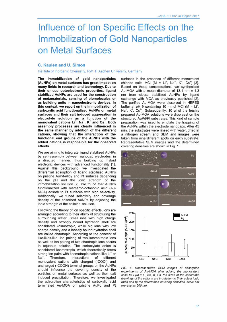
JARA-FIT Annual Report 2017
57
Influence of Ion Specific Effects on the Immobilization of Gold Nanoparticles on Metal Surfaces C. Kaulen and U. Simon Institute of Inorganic Chemistry, RWTH Aachen University, Germany The immobilization of gold nanoparticles (AuNPs) on metal surfaces has great impact on many fields in research and technology. Due to their unique optoelectronic properties, ligand stabilized AuNPs are used for the construction of metamaterials, sensing of biomolecules or as building units in nanoelectronic devices. In this context, we report on the immobilization of carboxylic acid functionalized AuNPs on metal surfaces and their salt induced aggregation in electrolyte solution as a function of the monovalent cations Li+, Na+, K+ and Cs+. Both assembly processes are clearly influenced in the same manner by addition of the different cations, showing that the interaction of the functional end groups of the AuNPs with the added cations is responsible for the observed effects.
We are aiming to integrate ligand stabilized AuNPs by self-assembly between nanogap electrodes, in a directed manner, thus building up hybrid electronic devices with advanced functionality [1]. Against this background, we investigated the differential adsorption of ligand stabilized AuNPs on pristine AuPd-alloy and Pt surfaces depending on the pH and the ionic strength of the immobilization solution [2]. We found that AuNPs functionalized with mercapto-octanonic acid (Au-MOA) adsorb to Pt surfaces with high selectivity. Additionally, we tuned selectivity and coverage density of the adsorbed AuNPs by adjusting the ionic strength of the colloidal solution.
Following the theory of ion specific effects, ions are arranged according to their ability of structuring the surrounding water. Small ions with high charge density and strongly bound hydration shell are considered kosmotropic, while big ions with low charge density and a loosely bound hydration shell are called chaotropic. According to the concept of like-likes-like, ion pairing of two kosmotropic ions as well as ion pairing of two chaotropic ions occurs in aqueous solution. The carboxylate anion is considered kosmotropic, which theoretically forms strong ion pairs with kosmotropic cations like Li+ or Na+. Therefore, interactions of different monovalent cations with charged (-COO-) and uncharged (-COOH) terminal groups on the AuNPs should influence the covering density of the particles on metal surfaces as well as their salt induced precipitation. Therefore, we investigated the adsorption characteristics of carboxylic acid terminated Au-MOA on pristine AuPd and Pt
surfaces in the presence of different monovalent chloride salts MCl (M = Li+, Na+, K+, Cs+) [3]. Based on these considerations, we synthesized Au-MOA with a mean diameter of 13.1 nm ± 1.3 nm from citrate stabilized AuNPs by ligand exchange with MOA as previously published [2]. The purified Au-MOA were dissolved in HEPES buffer at pH 9 containing 10 mmol MCl (M = Li+, Na+, K+, Cs+). Subsequently, 10 µl of the freshly prepared Au-MOA solutions were drop cast on the structured AuPd/Pt substrates. This kind of sample preparation was used to emulate the trapping of the AuNPs within the electrode nanogaps. After 45 min, the substrates were rinsed with water, dried in a nitrogen stream and SEM and images were taken from nine different spots on each substrate. Representative SEM images and the determined covering densities are shown in Fig. 1.
FIG. 1: Representative SEM images of adsorption experiments of Au-MOA after adding the monovalent salts MCl (M = Li, Na, K, Cs, the sizes of the schematic drawings of the cations are in relation to their actual ionic radii) and b) the determined covering densities, scale bar represents 500 nm.
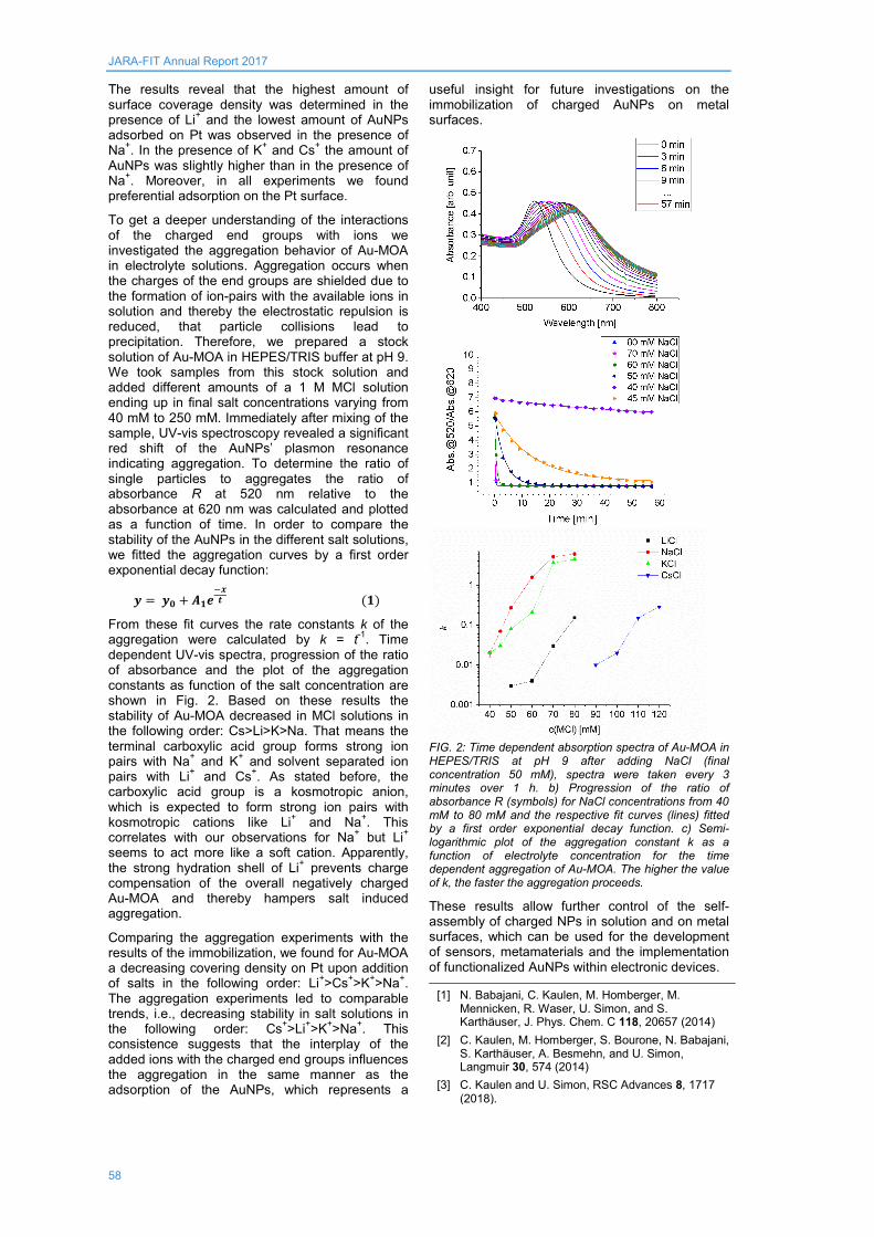
JARA-FIT Annual Report 2017
58
The results reveal that the highest amount of surface coverage density was determined in the presence of Li+ and the lowest amount of AuNPs adsorbed on Pt was observed in the presence of Na+. In the presence of K+ and Cs+ the amount of AuNPs was slightly higher than in the presence of Na+. Moreover, in all experiments we found preferential adsorption on the Pt surface.
To get a deeper understanding of the interactions of the charged end groups with ions we investigated the aggregation behavior of Au-MOA in electrolyte solutions. Aggregation occurs when the charges of the end groups are shielded due to the formation of ion-pairs with the available ions in solution and thereby the electrostatic repulsion is reduced, that particle collisions lead to precipitation. Therefore, we prepared a stock solution of Au-MOA in HEPES/TRIS buffer at pH 9. We took samples from this stock solution and added different amounts of a 1 M MCl solution ending up in final salt concentrations varying from 40 mM to 250 mM. Immediately after mixing of the sample, UV-vis spectroscopy revealed a significant red shift of the AuNPs’ plasmon resonance indicating aggregation. To determine the ratio of single particles to aggregates the ratio of absorbance R at 520 nm relative to the absorbance at 620 nm was calculated and plotted as a function of time. In order to compare the stability of the AuNPs in the different salt solutions, we fitted the aggregation curves by a first order exponential decay function:
𝒚 = 𝒚𝟎 + 𝑨𝟏𝒆−𝒙𝒕 (𝟏)
From these fit curves the rate constants k of the aggregation were calculated by k = t-1. Time dependent UV-vis spectra, progression of the ratio of absorbance and the plot of the aggregation constants as function of the salt concentration are shown in Fig. 2. Based on these results the stability of Au-MOA decreased in MCl solutions in the following order: Cs>Li>K>Na. That means the terminal carboxylic acid group forms strong ion pairs with Na+ and K+ and solvent separated ion pairs with Li+ and Cs+. As stated before, the carboxylic acid group is a kosmotropic anion, which is expected to form strong ion pairs with kosmotropic cations like Li+ and Na+. This correlates with our observations for Na+ but Li+ seems to act more like a soft cation. Apparently, the strong hydration shell of Li+ prevents charge compensation of the overall negatively charged Au-MOA and thereby hampers salt induced aggregation.
Comparing the aggregation experiments with the results of the immobilization, we found for Au-MOA a decreasing covering density on Pt upon addition of salts in the following order: Li+>Cs+>K+>Na+. The aggregation experiments led to comparable trends, i.e., decreasing stability in salt solutions in the following order: Cs+>Li+>K+>Na+. This consistence suggests that the interplay of the added ions with the charged end groups influences the aggregation in the same manner as the adsorption of the AuNPs, which represents a
useful insight for future investigations on the immobilization of charged AuNPs on metal surfaces.
FIG. 2: Time dependent absorption spectra of Au-MOA in HEPES/TRIS at pH 9 after adding NaCl (final concentration 50 mM), spectra were taken every 3 minutes over 1 h. b) Progression of the ratio of absorbance R (symbols) for NaCl concentrations from 40 mM to 80 mM and the respective fit curves (lines) fitted by a first order exponential decay function. c) Semi-logarithmic plot of the aggregation constant k as a function of electrolyte concentration for the time dependent aggregation of Au-MOA. The higher the value of k, the faster the aggregation proceeds.
These results allow further control of the self-assembly of charged NPs in solution and on metal surfaces, which can be used for the development of sensors, metamaterials and the implementation of functionalized AuNPs within electronic devices.
[1] N. Babajani, C. Kaulen, M. Homberger, M. Mennicken, R. Waser, U. Simon, and S. Karthäuser, J. Phys. Chem. C 118, 20657 (2014)
[2] C. Kaulen, M. Homberger, S. Bourone, N. Babajani, S. Karthäuser, A. Besmehn, and U. Simon, Langmuir 30, 574 (2014)
[3] C. Kaulen and U. Simon, RSC Advances 8, 1717 (2018).

JARA-FIT Annual Report 2017
59
TiO2 Nanoparticle Monolayers: Self-Assembly and Resistive Switching D. O. Schmidt1, N. Raab2, M. Noyong1, V. Santhanam3, R. Dittmann2, and U. Simon1 1 Institute of Inorganic Chemistry, RWTH Aachen University, Germany 2 Peter Grünberg Institut-7, Forschungszentrum Jülich GmbH, Germany 3 Department of Chemical Engineering, Indian Institute of Science, Bangalore, India Resistively switching is considered as highly promising technology for advanced non-volatile data storage. Up to now devices are fabricated following top-down routes that apply thin films sandwiched between electrodes. Previously we demonstrated that resistive switching (RS) is also feasible on chemically synthesized nanoparticles (NPs) having diameters in the 50 nm range. We now developed this approach further to the sub-10 nm range and thereby go below the size range achievable by means of lithographic techniques. In this work, we report RS of sub-10 nm TiO2 NPs that were self-assembled into monolayers and transferred onto metallic substrates. We electrically characterized these monolayers in regard to their RS properties by means of a nanorobotics system in a scanning electron microscope, and found features typical of bipolar resistive switching.
The increasing demand for digital data storage will require new, non-volatile data storage technologies in the near future. Resistive random access memories (RRAM) are promising candidates for such applications [1,2]. They rely on resistive switching (RS), which results from a resistance change of a functional layer sandwiched between metal electrodes. RRAM devices are typically composed of a metal–insulator–metal layer structure, mainly in the form of thin films that are structured by means of lithographic (top–down) techniques. As an alternative approach, nanoparticle (NP) thin films formed via chemical synthesis and assembly can be utilized as a functional layer in RS devices. Such a bottom–up approach in principle allows the fabrication of cell dimensions that exceed the size limits of top–down approaches. From a technological point of view, NPs can be synthesized via inexpensive methods and under mild reaction conditions. Subsequently, the NPs can be deposited on the electrodes using solution-based techniques that are suitable for organic or polymeric substrates, thus leading to flexible memory devices.
Recently, we reported the RS of individual TiO2 NPs with sizes as small as 50 nm [3]. In order to go below the size range achievable by means of lithographic techniques, we present now the synthesis and the self-assembly of sub-10 nm TiO2 NPs and their resistive switching properties.
The synthesis of the sub-10 nm TiO2 NPs followed a procedure first reported by Dinh et al. [4]. For this
purpose, titanium butoxide was used as titanium precursor, oleylamine and oleic acid were used as capping agents. Spherical NPs with anatase structure were obtained. For self-assembly and monolayer formation, the TiO2 NPs were dispersed in an organic solvent and were dropped on a water surface with a controlled surface curvature. Due to the evaporation of the organic solvent, a self-assembled monolayer was formed on the water surface. As can be derived from Fig. 1, extended continuous self-assembled NP monolayer films of approximately 1 µm2 in size were formed with close packing. Fourier transformation by means of the Software ImageJ (Version 1.43u) revealed the hexagonal symmetry of the particle packing with a center-to-center spacing of ca. (9 ± 1) nm, which corresponds to the dimensions of the NPs, plus the approximately 2 nm length of the oleic acid and oleylamine ligands.
FIG. 1: Exemplary TEM images of the self-assembled TiO2 NP film with decreasing magnification (a,b). The inset in (b) shows the fast Fourier transformation of the black highlighted area of the monolayer. Reprinted from [3].
For the RS experiments, the monolayers were transferred to Pt/Ir substrates by means of microcontact printing.
Images derived from TEM and AFM measurements indicate that the monolayers were successfully transferred to the Pt/Ir substrates. Fig.

JARA-FIT Annual Report 2017
60
2 displays an exemplary AFM image including the respective height profile.
FIG. 2: Exemplary AFM image of a TiO2 NP film after transferring to Pt/Ir surface (a) and the corresponding height profile (b). Reprinted from [3].
For the electrical measurements, a nanorobotics system in a FE-SEM was applied [5]. Prior to the switching experiments, oxygen plasma cleaning was applied to remove the oleylamine/oleic acid ligands. As top electrodes, we used Pt/Ir coated AFM tip. While the voltage was applied to the tip, the planar Pt/Ir bottom electrode was set to ground. A schematic illustration of the experimental setup and an exemplary SEM image are displayed in Fig. 3a, b, respectively.
FIG. 3: Schematic illustrations of the (Pt/Ir)/TiO2 NP film/(Pt/Ir tip) device (a). Exemplary SEM image of a TiO2 NP film on the Pt/Ir surface, exhibiting mono- and multilayers. On the left hand side, the Pt/Ir coated tip electrode is visible (b). Reprinted from [3].
The RS properties were tested with a current compliance of up to 10 µA to protect the TiO2 NP layer, as well as the metal coating of the measurement tips. The I–V curve shown in Fig. 4 was recorded on a TiO2 NP monolayer. It exhibits typical bipolar resistive switching (BRS) with a SET process of the device from the high resistance state (HRS) into the low resistance state (LRS) at a voltage of ca. −2.5 V. The RESET process occurred over a voltage range from 1.0 V to approximately 2.8 V, and switched the device back
into the HRS. As exemplary shown in Fig. 4, in most experiments, we observed counter eight wise switching polarity, whereby hysteresis and the current are larger at a negative voltage polarity compared with the positive voltage polarity.
FIG. 4: I–V curve recorded on a TiO2 NP monolayer exhibiting bipolar resistive switching (BRS) properties. The arrows and letters besides the plotted curves depict voltage sweep direction. Reprinted from [3].
In general, the switching polarity of a BRS device is determined by a microstructurally asymmetric cell design, or a voltage/current-controlled electroforming process. The underlying switching mechanism for valence change memories is generally explained by a formation and rupture of a conductive filament inside the insulating TiO2 matrix due to the redistribution of oxygen vacancies under an applied electric field, and the effect of Joule heating. This gives rise to a resistance hysteresis exhibiting the counter eight wise polarity.
In summary, we synthesized TiO2 NPs with a size below 10 nm by a solvothermal method. Self-assembly of TiO2 NP monolayers was achieved with dense packed monolayers in an area of 1 µm2. As the TiO2 NP films were prepared on a water surface, they had to be transferred onto metallic surfaces in order to subsequently electrically characterize the NPs. We successfully executed a microcontact printing to transfer the self-assembled film to Pt/Ir surfaces that acted as bottom electrodes during resistive switching experiments. The electrical characterization of the self-assembled TiO2 NP films on Pt/Ir bottom electrodes was performed by means of a nanorobotics setup SEM and revealed BRS-like behavior.
[1] R. Waser, R. Dittmann, G. Staikov, and K. Szot, Adv. Mater. 21, 2632 (2009).
[2] D. Ielmini, R. Waser, in Resistive Switching: From Fundamentals of Nanoionic Redox Processes to Memristive Device, Applications, 1st ed.; Wiley-VCH: Weinheim, Germany (2016).
[3] D. O. Schmidt, N. Raab, M. Noyong, V. Santhanam, R. Dittmann, and U. Simon, Nanomaterials 7(11), 370 (2017)
[4] C.-T. Dinh, T.-D. Nguyen, F. Kleitz, and T.-O. Do, Nanocrystals. ACS Nano 3, 3737 (2009)
[5] M. Noyong, K. Blech, A. Rosenberger, V. Klocke, and U. Simon, Meas. Sci. Technol. 18, N84 (2007)
a)
b)

JARA-FIT Annual Report 2017
61
Single crystalline superstructured stable single domain magnetite nanoparticles V. Reichel1, A. Kovács2, M. Kumari3, É. Bereczk-Tompa4, E. Schneck1, P. Diehle2, M. Pósfai4, A. M. Hirt3, M. Duchamp2, R. E. Dunin-Borkowski2, and D. Faivre1 1 Department of Biomaterials, Max Planck Institute of Colloids and Interfaces, Potsdam, Germany 2 Ernst Ruska-Centre for Microscopy and Spectroscopy with Electrons and Peter Grünberg Institute,
Forschungszentrum Jülich, Germany 3 Institute of Geophysics, ETH-Zürich, Switzerland 4 Department of Earth and Environmental Sciences, University of Pannonia, Veszprém, Hungary Magnetite nanoparticles exhibit magnetic properties that are size and organization dependent and, for applications that rely on their magnetic state, they usually have to be monodisperse. Forming such particles, however, has remained a challenge. We synthesize 40 nm particles of magnetite in the presence of polyarginine and show that they are composed of 10 nm building blocks, yet diffract like single crystals. We use both bulk magnetic measurements and magnetic induction maps recorded from individual particles using off-axis electron holography to show that each 40 nm particle typically contains a single magnetic domain. The magnetic state is therefore determined primarily by the size of the superstructure and not by the sizes of the constituent sub-units. Our results fundamentally demonstrate the structure – property relationship in a magnetic mesoparticle [1].
Magnetite is a ubiquitous iron oxide mineral that is found on Earth and in planetary settings, as well as in the biological world. Magnetite nanoparticles have numerous industrial and technological applications, which often require well-defined magnetic behaviour. The magnetic properties of magnetite are dependent on Néel relaxation, which in turn depends on particle size, morphology and interparticle interactions, as well as on the temperature and time-scale of the measurement. For example, for a measurement time of 100 ms at room temperature, isolated equidimensional magnetite particles that have diameters of less than approximately 25 nm are superparamagnetic (SP), i.e., the directions of their magnetic moments change due to thermal fluctuations on the order of the measurement time. Particles with diameters of approximately 25 to 80 nm are typically magnetized homogeneously and considered to be stable single domain (SSD), i.e., thermally blocked, magnetic states with uniform magnetization. Particles that are larger than 80 nm are usually multi-domain (MD), i.e. each particle is split into magnetic domains. Synthesized magnetite nanoparticles are generally considered to be individual magnetic units. However, magnetite
superstructures have been reported that are based on sub-units potentially too large to display SP behaviour, while the particles themselves are too large to display SSD behaviour. Here, we show that the addition of polyarginine to aqueous solution [2] mostly leads to the formation of 40 nm monodisperse magnetite particles that are made from 10 nm sub-domains, yet possess true SSD properties.
FIG. 1: (a) HAADF STEM and (b) BF TEM images of magnetite particles assembled into chains. The particles display light and dark contrast in (a) and (b), respectively. The web-like feature in the background in (b) is a lacey C support film. The inset in (b) shows the particle size distribution, as measured from TEM images.
Transmission electron microscopy (TEM) is used to study the sizes, shapes, structures and compositions of the particles, as well as the crystallographic orientations of individual nanocrystals within particles. The nanoparticles were found to distribute themselves into two-dimensional clusters or self-organized chains when deposited on TEM grids (Fig. 1(a) and (b)). The measured size distribution of the particles indicates that they are monodisperse, with a mean diameter of 36.7 ± 3.7 nm (inset to Fig. 1(b)).
We use off-axis electron holography (EH) in the TEM to study the magnetic induction associated with individual magnetite particles arranged in rings and chains, in order to examine the magnetization states within the mesocrystals and

JARA-FIT Annual Report 2017
62
interactions between them. A representative magnetic induction map recorded from a ring of six magnetite particles demonstrates that each particle contains a single magnetic domain (Fig. 2(a)), while the ring configuration of the particles constrains the magnetic field to form a flux-closed state. A similar magnetic induction map of a chain configuration also indicates that most of the particles are single magnetic domains, with the direction of the magnetic induction now determined by the overall direction of the chain (Fig. 2(b)). Two of the largest (ca. 50 nm) particles that are visible in Fig. 2(b), however, appear to have multi-domain states, as suggested by the changes in the directions of the contour lines and colours within them. Each 40 nm magnetite particle can be regarded as a “magnetic mesoparticle”. It is composed of a number of SP sub-units but its magnetic properties are determined by the size of the superstructure, rather than that of its components, reminiscent of the structural properties of mesocrystals.
We also analyse the bulk magnetic properties of the sample. The nanoparticles showed a thin hysteresis loop, with a coercivity Hc of 4.2 mT. The magnetization is saturated by 200 mT, while the ratio of saturation remanent magnetization (Mrs) to saturation magnetization (Ms) is 0.29. A backfield isothermal remanent magnetization (IRM) curve is saturated by approximately 150 mT. These results indicate that the synthesized magnetite is pure and shows no significant degree of oxidation.
We speculate on the possible mechanism that results in the controlled organization of the sub-units. We performed syntheses over prolonged periods of time (up to 5 h), but did not observe particle growth. the formation of our particles does not occur by simple stabilization of primary particles by polyarginine but is thought to occur in a three-stage process, whereby the particles first form and then aggregate into magnetite nanoparticles (our sub-units) with sizes of approximately 10 nm. This size agrees well with the sizes of the sub-units observed in the 40 nm particles. The sub-units possibly aggregate via oriented attachment. A potential reason for this behaviour is that the magnetite surface is negatively charged at the pH of our synthesis whereas the guanidine group of polyR is positively charged. As a result, polyR may serve as an “electrostatic glue” for the aggregation of the sub-units, similarly to what has been observed for ellipsoid hematite particles. The uniform sizes of our particles demonstrate that the synthesis method leads to SSD magnetite particles with a narrow particle size distribution, despite the fact that the particles are made of smaller SP sub-units.
FIG. 2: Magnetic induction maps recorded in magnetic field-free-conditions using off-axis electron holography from (a) a ring and (b) a chain of magnetite particles. The colours and contours show the direction and strength of the projected in-plane magnetic flux density, respectively. A colour wheel is shown as an inset at the lower left corner of each image. The magnetic phase contour spacing is 2π/256 radians in each image. The white arrows indicate the direction of the magnetic induction in each particle. A thin white line marks the outer edge of each particle.
In summary, we have used 40 nm magnetite particles composed of ca. 10 nm sub-units as a model system to study the relationship between the structures and magnetic properties of nanoscale magnetite particles. We have shown that the magnetic properties of each magnetite mesocrystal are dominated by those of the superstructure.
[1] V. Reichel et al., Scientific Reports (Nature) 7, 45484 (2017)
[2] J. Baumgartner et al., Nat. Mater. 12, 310 (2017)

JARA-FIT Annual Report 2017
63
Direct imaging of a zero-field target skyrmion and its polarity switch in a chiral magnetic nanodisk F. Zheng1, H. Li2, S. Wang3,4, D. Song5, C. Jin3,4, W. Wei3,4, A. Kovács1, J. Zang2, M. Tian3,4, Y. Zhang3,4, H. Du3,4, and R. E. Dunin-Borkowski1 1 Ernst Ruska-Centre for Microscopy and Spectroscopy with Electrons and Peter Grünberg Institute,
Forschungszentrum Jülich, Germany 2 Department of Physics, University of New Hampshire, Durham, USA 3 The Anhui Key Laboratory of Condensed Matter Physics at Extreme Conditions, High Magnetic Field
Laboratory, Chinese Academy of Sciences and University of Science and Technology of China, Hefei, China
4 Collaborative Innovation Center of Advanced Microstructures, Nanjing University, Jiangsu Province, China
5 National Center for Electron Microscopy in Beijing, Key Laboratory of Advanced Materials (MOE) and the State Key Laboratory of New Ceramics and Fine Processing, School of Materials Science and Engineering, Tsinghua University, Beijing, China
A target skyrmion (Sk) is a flux-closed spin texture that has two-fold degeneracy and is promising as a binary state in next generation universal memories. Although its formation in nanopatterned chiral magnets has been predicted, its observation has remained challenging. We use off-axis electron holography (EH) to record images of target Sks in a nanodisk of the chiral magnet FeGe. We compare experimental measurements with numerical simulations, demonstrate switching between two stable degenerate target Sk ground states that have opposite polarities and rotation senses and discuss the observed switching mechanism [1].
Magnetic Sks, which are characterized by topological indices, exhibit novel dynamics and are of interest as carriers of binary digits or logic elements in future spintronic devices. The engineering difficulty and energy consumption of such devices would be reduced by the realization of zero-field Sk states. The stabilization of Sks in chiral magnets usually results from a combination of ferromagnetic exchange, anti-symmetric chiral Dzyaloshinskii-Moriya (DM) interactions and the presence of an externally applied magnetic field, with the first two coupling terms giving rise to a spin helix ground state. However, a zero-field Sk is predicted to be possible in a nanopatterned structure because the magnetostatic energy then prefers a flux-closed state. This exotic topological texture is termed target skyrmion.
A major obstacle that hinders the imaging of the magnetic texture of a target Sk is the fact that the size of the nanodisk that supports it must be comparable to the size ask of the Sk itself (<100 nm). The study of smaller samples by Lorentz transmission electron microscopy (TEM) has been hindered both by sample preparation and by limitations in the spatial resolution of magnetic
imaging techniques. Such unwanted contributions to the recorded contrast can be eliminated more easily when using off-axis electron holography (EH) in the TEM [2]. EH has been used to provide direct access to magnetic phase shift and projected in-plane magnetization of FeGe thin films with nm spatial resolution [3].
FIG. 1: ( a, b) Magnetization configurations of two-fold-degenerate target skyrmions for p = -1 and p = +1, respectively. (c, d) In-plane magnetization in the target skyrmions in (a) and (b), respectively with colors and arrows used to indicate the rotational sense of the in-plane magnetization, according to the color wheel shown. The black dashed lines in (a) and (b) and the thin red lines in (c) and (d) mark the boundaries between the skyrmions and the circular edge twists.
A target Sk consists of a central Sk surrounded by one or more concentric helical stripes (Fig. 1) and

JARA-FIT Annual Report 2017
64
can be regarded as a curved spin helical state. From the center of the disk to its boundary, the out-of-plane component of the magnetic moment rotates by an angle ϕ that is larger than the value of π for a typical Sk. As a result of the boundary confinement, the outermost spin helix, which is termed an edge twist, may correspond to an irrational fraction of a period. There are two parameters—the polarity p and the circularity c — to describe the direction of the out-of-plane magnetization at the center of a target Sk and the rotational sense of its in-plane magnetization, respectively. The out-of-plane magnetization at the core can point either up (p=+1) or down (p=-1), while the in-plane magnetization can rotate either clockwise (c=+1) or counterclockwise (c=-1). The circularity c of the center Sk and the edge twist have opposite values. As a result of the fixed handedness and sign of the DM interaction, c is determined uniquely once p has been defined. In zero magnetic field, two degenerate configurations with opposite magnetization are possible as a result of the quadratic nature of the Heisenberg and DM interactions.
The first image in Fig. 2(a), also final in Fig. 2(b), shows a representative magnetic induction map of the nanodisk recorded using EH after zero-field cooling (ZFC). The central region with circularity c=-1 is a complete Sk surrounded by an edge twist for which c=+1. We label this target Sk Type 1. As mentioned above, target Sk with opposite polarity have the same energy in zero magnetic field. The same ZFC annealing procedure was used to obtain a magnetic state in which the central Sk corresponded to c=+1 (first image in Fig. 2(b)). This target Sk is labeled Type 2. In order to switch between two degenerate states, we applied a magnetic field B perpendicular to the disk. For the Type 1, an increase in applied magnetic field shrinks the central Sk, while both c and p are unchanged during the magnetization process until a saturated magnetic state is achieved at large B (Fig. 2(a)) indicating that the polarity of this target Sk is p=−1. Interestingly, the size of the central Sk exhibits a non-monotonic dependence on applied magnetic field and has a maximum value of 110 nm at B=134 mT, which is almost 1.5 times ask.
A different process is observed for a Type 2 target Sk, as shown in Fig. 2(b). At low values of B between 0 and 67 mT, the size of the central Sk decreases, while that of the edge twist increases. Above a threshold value of B=134 mT, expansion of the edge twist cannot be sustained and it splits into a half-period spin helix and a new edge twist outside it. Not considering the new edge twist, the newly formed spin texture is referred to as a 2π vortex because the rotation angle ϕ from the center to the edge is exactly 2π. The circularity (c=−1) in the new half period helix is opposite to that of the central Sk, while for the new edge twist c=+1. When the external field exceeds 200 mT, the central Sk shrinks and ultimately disappears. At the same time, the half-period circular helix takes over and evolves into a new Sk by collapsing its inner ring to a single point. The circularity of the newly formed central Sk is c=−1, which follows the initial
circular edge twist at B=0 mT. c is then opposite to that of the initial target Sk. As a result of the relationship between the polarity and the circularity, the polarity is also switched. The switching field Bs from an initial 2π vortex to the new π vortex is ~220 mT. Once the polarity reversal of the target Sk has been achieved, a decrease in the field does not change the polarity (final image in Fig. 2(b)).
FIG. 2: Magnetic induction maps recorded using off-axis electron holography showing target skyrmions in an FeGe nanodisk for different applied magnetic fields. (a) Target skyrmion of Type 1 with p = -1. The circularity and polarity persist during the entire magnetization process. (b) Target skyrmion of Type 2 with p = +1. In an intermediate applied field, a new half-period curved spin helix forms between the central skyrmion and the edge twist (panel b, H ~ 134, 167 and 200 mT). In a higher applied field, the target skyrmion evolves to the other type (panel b, H ~ 233 and 267 mT). The thick white arrows show the direction of rotation of the projected in-plane magnetic induction. ⊙ and represent up and down orientations, respectively.
We performed numerical simulations using a spin model for a 3D isotropic chiral magnet, in order to understand the spin arrangement and magnetic phase transitions in more detail. The results show that the target Sk always has a lower energy than any other magnetic state, indicating that the ground state is consistent with the experimental results, and also confirm that both the demagnetization energy and the magnetization variation normal to the disk plane stabilize a zero-field target Sk.
In summary, We have directly observed zero-field target skyrmions in a chiral magnet FeGe in a strongly confined nanodisk geometry using state-of-the-art off-axis electron holography. In the presence of an external magnetic field applied perpendicular to the nanodisk, the two types of target Skyrmion can be switched.
[1] F. Zheng et al., Phys. Rev. Lett. 119, 197205 (2017).
[2] P. A. Midgley and R. E. Dunin-Borkowski, Nat. Mater. 8, 271 (2009).
[3] A. Kovács et al., Appl. Phys. Lett. 111, 192410 (2017).

JARA-FIT Annual Report 2017
65
Dynamical amplification of magnetoresistances and Hall currents up to the THz regime F. S. M. Guimarães1, M. dos Santos Dias1, J. Bouaziz1, A. T. Costa2, R. B. Muniz2, and S. Lounis1 1 Peter Grünberg Institut and Institute for Advanced Simulation, Forschungszentrum Jülich, Germany 2 Instituto de Física, Universidade Federal Fluminense, Niterói, Brazil The relativistic interaction between the spin and orbital degrees of freedom is the origin of a multitude of fascinating phenomena. Understanding these inherently dynamical processes is crucial to improve present-day reading and writing technology. On the one hand, the flow of electrons (the electric current) is influenced by the direction of the magnetization, giving rise to magneto-resistive effects. These are used in sensing devices for reading information stored in magnetic media. On the other hand, electric currents can apply (spin-orbit) torques on a magnetic unit, setting it into precessional motion or even switching its orientation. In this work, we investigate Co/Pt and Fe/W bilayers to uncover how the dynamical current-induced magnetic excitations, reaching the THz range, influence the flow of electrons through the system. Using a material-specific approach based on first-principles calculations, we prove that in-phase and out-of-phase processes can greatly magnify or suppress longitudinal and transverse currents, impacting all kinds of magnetoresistances and Hall effects.
In Ref. [1], we study how the electric current induces magnetization dynamics, and its intrinsic feedback to the current that drives it. To this end, we consider metallic bilayer heterostructures, consisting of a ferromagnetic (FM) metal deposited on a heavy metal (HM) substrate, combining magnetism with a strong spin-orbit interaction (SOI). The system is under the influence of a time-dependent uniform electric field given by 𝐄(𝑡) =Re[𝐸0𝑒𝑖𝑖𝑖𝐱], where 𝐸0 is the field amplitude and 𝜔 its angular frequency. An electric current may be measured along the longitudinal (x) or along the transverse (y) direction. The induced first order currents flowing through the system can be summarized in vector form as
𝐈C(𝑡) = Re𝐼𝑖,∥𝐱 + 𝐼𝑖,⊥𝐲𝐸0𝑒𝑖𝑖𝑖, (1)
where both longitudinal and transverse components are composed by in-phase 𝐼𝑖′ and out-of-phase 𝐼𝑖′′ components, i.e., 𝐼𝑖 = 𝐼𝑖′ + 𝑖𝐼𝑖′′.
A schematic setup and our choice of axes are depicted in Fig. 1. The total electric current flowing across the system can be split into two parts: 𝐈C(𝑡) = 𝐈C0(𝑡) + 𝐈C
dyn(𝑡), where the first term is the
current driven directly by the electric field, and the second is the dynamical part produced by the magnetization precession. The frequency dependence of 𝐈C0(𝑡) can be well described by the Drude model in metallic materials, and exhibits very little variation in the energy range we are interested in (on the order of a few meV).
FIG. 1: Spin-orbit-related mechanisms in a ferromagnetic/heavy metal bilayer. (a) An ac electric field is applied to the sample, driving a charge current through the system and generating an oscillatory spin accumulation 𝛿𝒔 ∝ 𝒛 × 𝑬(𝑡) on the surfaces of the heavy metal (HM). (b-d) At the interface between the heavy metal and the ferromagnetic (FM) layer, 𝛿𝒔 interacts with its magnetization 𝒎0. Depending on the direction of 𝒎0, the magnetization can be set into precession, pumping charge and spins back into the heavy metal, thereby contributing to the (longitudinal and/or transverse) current flowing across the system.
The dynamical contribution, 𝐈Cdyn(𝑡), which is the
main focus of this work [1], originates from a combination of several mechanisms as follows: Due to the SOI, an oscillatory spin accumulation is induced at the heavy metal surfaces, as illustrated in Fig. 1a. Different processes contribute to the accumulation, such as the flow of a transverse spin current (spin Hall effect) that reaches the edges, or a change in the electronic occupations induced by the external field (Rashba-Edelstein or inverse spin galvanic effect). Then, spin-orbit torques may set the magnetic moment of the FM layer into precessional motion, depicted in Figs. 1(b-d). Note that when 𝐦0 ∥ 𝐲, no precession is induced. Finally, spin pumping followed by inverse spin Hall effect and charge pumping generated by spin- galvanic effects produce the additional charge current 𝐈C
dyn(𝑡), as shown in Figs. 1(c,d).

JARA-FIT Annual Report 2017
66
The behavior of the longitudinal and transverse in-phase currents, 𝐼𝑖,∥ and 𝐼𝑖 ,⊥ respectively, calculated as functions of the applied electric field frequency, for different thicknesses of the Pt substrate in a Co/Pt(001) bilayer is shown in Fig. 2. A drastic variation is observed for the currents as the frequency is varied. The structures manifested in the currents are related to the ferromagnetic resonances of the magnetic layers, located at frequencies determined by the magnetic anisotropy. They induce substantial changes owing to the pumping mechanisms described earlier, which clearly affect both the longitudinal and transverse currents. The thickness-dependent variations reflect quantum well effects present in out atomically thin films.
The excitation of the spin waves and, therefore, the pumping effects depend on the relative angle between the magnetization and the induced spin accumulation at the interface of the bilayer. By
applying a large magnetic field to orient the magnetization along any chosen direction, we calculate the angular dependencies of the in-phase longitudinal and transverse currents as a function of the frequency. In Fig. 3, we show this result as a colorcoded map when the magnetization is rotated in the xy-plane. Note that when 𝐦0 ∥ 𝐲, the precession is not excited (Fig. 1b) and no enhancement is obtained. On the lower plots we display cuts for the static field and in the vicinity of the resonance frequency to demonstrate the substantial increase obtained in the currents.
To conclude, we remark that taking into account the dephasing between the processes is crucial for a correct description of the dynamical quantities. In Ref. [1], we demonstrate that the spin Hall angle, a common quantity used to quantify the conversion between charge and spins currents, is better described as a complex number instead of a real
one. We also present results on Fe/W(110) bilayers that exhibits remarkably distinct modifications and intricate angular dependencies.
We gratefully acknowledge the computing time granted by the JARA-HPC Vergabegremium and VSR commission on the supercomputers JURECA and JUQUEEN at Forschungszentrum Jülich. We thank the support of CNPq (Brazil) and Alexander von Humboldt foundation (Germany). This work was funded by the HGF-YIG Programme VH-NG-717 (Functional Nanoscale Structure and Probe Simulation Laboratory-Funsilab) and the European Research Council (ERC) under the European Union's Horizon 2020 research and innovation programme (ERC-consolidator grant 681405 – DYNASORE).
[1] F. S. M. Guimarães, M. dos Santos Dias, J. Bouaziz, A. T. Costa, R. B. Muniz, and S. Lounis, Sci. Rep. 7, 3686 (2017)
FIG. 3: Dependence of the charge currents on the direction of the magnetization and on the frequency of the applied electric field. (a) Longitudinal and (b) transverse currents for Co/Pt(001), illustrated as a colormap (top) and cuts (bottom) corresponding to an applied dc field (dashed lines) and close to the resonance frequency (solid lines).
FIG. 2: Dependence of the charge currents on the frequency of the applied electric field. (a) Longitudinal and (b) transverse in-phase currents calculated for monolayers of Co/Pt(001) as functions of the frequency, for different number of layers of Pt. The magnetization is normal to the surface due to the easy axis anisotropy of the system.

JARA-FIT Annual Report 2017
67
Entropy production in photovoltaic cell M.H. Ansari Peter Grünberg Institut-2, Forschungszentrum Jülich, Germany Industrial photocell technology has reached a saturation in producing maximum power in converting solar energy to electricity. With the developments of quantum technology and the possibility to make artificial atoms with long coherent times, it is attractive to study how quantum technology can help increase the efficiency. An important measure of thermodynamics is entropy production. We evaluate the entropy production of a photovoltaic cell that is modelled by four electronic levels resonantly coupled to thermally populated field modes at different temperatures. We show that entropy flow in the cell depends on the quantum coherence time and the degeneracy lifting in the ground states. Interestingly, we identify a lower bound for entropy production, which sets limitations on the statistics of dissipated heat in the photocells. We characterize regimes where reversal flow of entropy can take place in the opposite direction that heat flows. This opens up the possibility to engineer photocells with enhanced output power.
In the past decade a number of physical quantities, such as charge and spin, have been accurately measured in quantum systems, and these measurements have found practical applications in superfast computation. More recently, energy flow has also been measured with high precision on superconducting circuits, although in the preliminary step and in absence of full quantum features [1].
Quantum heat engines (QHE) have been recently studied and already found applications in various physical systems such as light-harvesting biocells, photovoltaic cells, laser industry, [2]. The QHE of our interest here has been introduced by Scully [2], which has four energy levels, two nearly degenerate ground states and the other two excited states. This quantum system, Fig. 1, is weakly coupled to two large heat reservoirs kept at temperatures Tc and Th and externally driven by a frequency equal to the energy difference of the two excited states. Heat dissipations has been previously studied for this QHE and showed lasing without inversion and elevated output working power [3].
A semiclassical approach has been taken to predict the entropy production, then the classical second law of thermodynamics has also been used to estimate the work produced by the cells. We noticed, however, that there are a number of limitations and inconsistencies in these analysis. Entropy is one of the central quantities in thermodynamics, whose consistent evaluation determine many features of the heat engines. In
quantum theory evaluating entropy production sometimes contradicts classical evaluation. The reason is mainly in that entropy is nonlinear in density matrix; S=-kB Tr(𝜌 ln(𝜌)), with 𝜌 being density matrix. Recently a consistent formalism has been proposed to evaluate entropy production in quantum systems in the weak coupling regime. [4]. An exact correspondence is also found to link this entropy production to the full counting statistics of heat dissipation in the quantum system [5].
FIG. 1: A photovoltaic cell: A doubly-degenerate ground states (with detuning 𝛿) resonantly coupled to two classical heat reservoirs kept at different temperatures and driven with frequency equal to energy different between two excited states.
Here, we use the new formalism to consistently evaluate entropy production for the photovoltaic cell [6]. Using the exact correspondence between entropy production and statistics of energy transfer we understand exactly how energy is transferred in the QHE and how work is produced. The interesting feature that makes our work distinct from other approaches is that here we are faithful to quantum mechanics and do not take anything from classical physics for granted in quantum system. Our result shows interesting features in the entropy flow that cannot be determined from semiclassical analysis.
We find that entropy production is the difference of two parts: a linear production and a nonlinear production. The linear part depends on energy level population probabilities and the nonlinear term depends quadratically on off-diagonal elements of density matrix. For intermediate values of driving force amplitude, the nonlinear entropy production is equally as important as other terms. Fig. 2 the nonlinear entropy production is denoted with (blue curves) Fc and the linear entropy production with (red curves) Fi. The linear part turns out to be total entropy production semiclassical analysis predicts, this obviously semiclassical analysis ignores an important

JARA-FIT Annual Report 2017
68
contribution from quantum physics. We find that the total entropy production of this quantum heat engine has non-vanishing nonlinear terms; thus dS/dt=Fi-Fc.
FIG. 2: The linear (semiclassial) part Fi and nonlinear part Fc of entropy flow as the function of cold reservoir temperature for two different quantum coherence times 𝜏=5 and 10𝜇s.
We also find that quantum coherence time affects entropy production in these cells. A cell with lower coherence time can much faster produce entropy. We compare two different cells with different coherent times of t = 5 and 10 ms. As shown in Fig. 2, in a cell with longer coherence time entropy production takes place with a completely different rate that what semiclassical approach predicts. This variation will modify the amount of work in terms of electric power that is produced by these cells. Depending on what is the cell coherence time its maximum power reach as well as engine efficiency get updated.
Another prediction of our analysis is that by lifting the degeneracy 𝜹 of the two ground states by a very small amount, entropy production can change by a large amount. Fig. 3 shows semiclassical and nonlinear entropy flows for two QHEs with 𝜹=0 (dotted) and 0.07Eh (solid). Lifting the degeneracy will shift entropy production down, which means that for small Tc the flow of entropy from cold to hot will take place faster, and for large Tc the flow from hot to cold bath will be slower. The nonlinear production in this case is almost negligible except at very cold Tc.
As shown in Fig. 2 and 3 at a turning temperature (Tturn) the sign of entropy flow changes. This is in fact mainly due to the contribution of quantum coherence (off-diagonal elements of density matrix). If the cold reservoir temperature Tc<Tturn entropy flow is negative, which can be interpreted that entropy flows from hot to cold reservoirs. However if Tc>Tturn it changes the direction and flows from cold to hot. Here we are assuming Th is normalized to 1.
Another interesting feature of entropy production that we find from our analysis is that from Fig. 2 changing coherence time does not influence the turning temperature Tturn. However lifting degeneracy from 0 to the small amount of 0.07Eh will increase turning temperature Tturn by almost 20%. The reason is mainly in the fact that lifting degeneracy will reduce quantum coherence of ground states. Given that quantum coherence is mainly the reason for entropy reversal flow the increases of turning temperature is effectively to compensate quantum coherence reduction.
FIG. 3: The linear (semiclassial) part Fi and nonlinear part Fc of entropy flow for two different degeneracy lifting energy values 𝜹=0 and 0.07Eh .
We also find a condition that if satisfied quantum coherence will be influential on the photovoltaic cell functionality, otherwise the cell remains mainly semiclassical. This indicates the presence of a lower bound on entropy production below which no quantum effect is expected. Such a lower bound can only be found due to the presence of the nonlinear entropy production that we found to exist in these cells [6].
Further progress can be made to evaluate the dependence of work production of these cells as a function of quantum features of the cells, such as quantum coherence time. This will indicate the physical domain of parameters to fabricate more efficient cells with higher maximum powers production.
[1] J.P. Pekola, Nature Physics 11, 118 (2015) [2] K.E. Dorfmana, D.V. Voroninea, S. Mukamelc,
M.O. Scully, Proc. Natl. Acad. Sci. USA 2746 (2013)
[3] M.O. Scully, K.R. Chapin, K.E. Dorfman, M.B. Kim, A. Svidzinsky, Proc. Natl. Acad. Sci. USA 108, 15097 (2011)
[4] M. H. Ansari, Yu. V. Nazarov, Phys. Rev. B 91, 104303 (2015)
[6] M.H. Ansari, Phys. Rev. B 95, 174302 (2017)

JARA-FIT Annual Report 2017
69
CVD graphene for inverted spin valve devices fabricated by dry-transfer methods M. Drögeler1, L. Banszerus1,2, F. Volmer1, T. Taniguchi3, K. Watanabe3, C. Stampfer1,2, and B. Beschoten1 1 II. Institute of Physics, RWTH Aachen University, Germany. 2 Peter Grünberg Institute-9, Forschungszentrum Jülich, Germany. 3 National Institute for Materials Science, Namiki, Tsukuba, Japan. Integrating high-mobility graphene grown by chemical vapor deposition (CVD) into spin transport devices is one of the key tasks in graphene spintronics [1]. We make use a van der Waals pickup technique to transfer CVD graphene by hexagonal boron nitride (hBN) from the copper growth substrate onto predefined Co/MgO electrodes to build inverted spin valve devices. Two approaches are presented: (i) a process where the CVD-graphene/hBN stack is first patterned into well-defined geometries and then transferred by a second larger hBN crystal onto spin valve electrodes and (ii) a direct transfer of a CVD-graphene/hBN stack. We report record high spin lifetimes in CVD graphene of up to 1.75 ns at room temperature. Overall, the performances of our devices are comparable to devices fabricated from exfoliated graphene also revealing nanosecond spin lifetimes. We expect that this dry transfer method paves the way towards more advanced device geometries not only for spintronic applications but also for CVD-graphene-based nanoelectronic devices for which patterning of the CVD graphene into sophisticated geometries may be required to unlock further device functionalities. In the field of graphene spintronics, the introduction of a van der Waals pick-up technique to protect graphene by hBN has led to a tremendous improvement in spin and charge transport properties. So far the best device performance has been achieved for exfoliated graphene which was picked up by a large hBN crystal and subsequently transferred on pre-patterned Co/MgO electrodes yielding spin lifetimes of 12 ns, spin diffusion lengths of 30 µm, combined with charge carrier mobilities of more than 20,000 cm2/(Vs) at room temperature [2]. In contrast, state-of-the-art CVD-graphene-based spin valve devices exhibit minor charge and spin transport properties with spin lifetimes typically below 1 ns and carrier mobilities up to 2,000 cm2/(Vs) [3,4]. This is most likely caused by a wet transfer process, which was used in these studies to delaminate CVD graphene from the growth substrate (Cu foil). Here, we show inverted spin valve devices based on dry-transferred CVD-graphene. CVD-graphene
is grown by low pressure chemical vapor deposition on the inside of a copper enclosure which typically results in large graphene flakes of up to a few hundred micrometers (see Fig. 1e) [6]. The flakes are stored under ambient conditions for some days to allow for oxidation along the copper-to-graphene interface. This oxidation weakens the graphene-to-copper adhesion which allows the subsequent pick-up of the CVD graphene (Fig. 1a). This is done by an hBN crystal which was exfoliated onto a stack of polydimethylsiloxane (PDMS), polyvinylalcohol (PVA) and polymethylmethacrylate (PMMA). As the CVD graphene gets ripped along the outer edges of the hBN crystal, this CVD-graphene/hBN stack has the arbitrary shape of the exfoliated hBN flake. Therefore, we transfer this stack onto a clean Si/SiO2 substrate, dissolve the polymer stack in deionized water (DI), acetone and isopropanol and subsequently etch a well-defined geometry (Fig. 1b) by reactive ion etching (RIE). The desired shape of the graphene/hBN stack is defined by an aluminum hard mask made by electron beam lithography and a lift-off process and subsequently etched by RIE in an Ar/SF6 plasma (Fig. 1b). After the etching, the aluminum is removed using tetramethylammonium hydroxide (TMAH). In a next step, we pick up the CVD-graphene/hBN bar with a second, larger hBN crystal (Fig. 1c) and place the whole stack onto prepatterned Co/MgO electrodes (see Fig. 1d). The magnetic electrodes are fabricated on a Si++/SiO2 substrate (see Fig. 1d) using standard electron beam lithography, molecular beam epitaxy and a lift-off process. The electrodes consist of 35 nm Co followed by 1.0 nm of MgO. The latter is used as a spin injection and detection barrier.
An optical image of a device which was fabricated using this kind of process is shown in Fig. 1f. The yellow stripe in the center of the electrode structure represents the patterned graphene/hBN bar whereas the larger hBN crystal which was used for the transfer of the patterned hBN/Gr-stack shows up as the blue large flake. It is important that throughout the whole process the CVD graphene (see Fig. 1e) is protected by the hBN against solvents, polymers and the metal hard mask which is used for the RIE-etching step. Again, we first exfoliate hBN on a stack of PMMA/PVA/PDMS.

JARA-FIT Annual Report 2017
70
FIG. 1 (a)–(d) Illustration of the two different fabrication processes. (a) After the growth of the CVD-graphene on a copper foil, it is picked up with hBN. (b) The CVD-graphene/hBN stack is deposited on Si/SiO2 and the stack (dotted line) is etched by reactive ion etching to pattern the desired shape. (c) The etched hBN/graphene bar is picked up using a second hBN crystal and (d) placed on pre-structured Co/MgO electrodes. (e) Optical image of CVD-graphene on the copper foil after oxidation of the graphene-to-copper interface. (f) Optical image of a finished CVD-graphene spin valve fabricated by the etching technique. (g) Optical image of a CVD-graphene spin valve device fabricated by the stamping technique where the graphene is ripped from the CVD flake along the outer edges of an hBN stamp and directly deposited on the pre-patterned Co/MgO electrode structure. (h) Spin lifetime vs. gate voltage measured at a temperature of 300 K.
For the stamping the respective edges of the CVD and the hBN crystal are aligned in such a way that the overlap region of both flakes defines a stripe in the CVD graphene (see dashed line in Fig. 1a and label "hBN (ii)"). The pick-up of the stripe is feasible since there is only a strong adhesion between graphene and hBN but not between PMMA and graphene. Thereafter, the stack of PDMS/PVA/PMMA/ hBN/graphene is aligned and transferred to a predefined Co/MgO electrode structure. In a last step the whole stack is put in acetone and isopropanol to remove the polymer.
An optical image of one final device fabricated by this second process is shown in Fig. 1g. Although the graphene flake is not visible through the thick hBN crystal, confocal Raman spectroscopy is able to map the exact position and shape of the CVD-graphene flake below the top hBN. A corresponding Raman map of graphene’s 2D peak is depicted in the inset of Fig. 1g.
CVD-graphene-based spin valve devices fabricated by one of these two processes show comparable spin transport properties to devices based on exfoliated graphene [5].
The room temperature spin lifetimes of typical devices show the well-known V-shape dependence as a function of back gate voltage, i.e. charge carrier density (see Fig. 1h) with values reaching 1.75 ns. This value is the longest spin lifetime measured for CVD graphene by now and compares well to the average values obtained for inverted spin valve devices where we use exfoliated graphene flakes [2].
The nanosecond spin lifetimes indicate that there is no significant spin scattering at, for example, copper residues on the surface of the transferred CVD graphene which might be expected as a result from the CVD growth in the copper enclosures [7,8].
[1] S. Roche, J. Åkerman, B. Beschoten, J.-C. Charlier, M. Chshiev, S. P. Dash, B. Dlubak, J. Fabian, A. Fert, M. Guimarães, F. Guinea, I. Grigorieva, C. Schönenberger, P. Seneor, C. Stampfer, S. O. Valenzuela, X. Wainta, and B. van Wees, 2D Materials 2, 030202 (2015)
[2] M. Drögeler, C. Franzen, F. Volmer, T. Pohlmann, L. Banszerus, M. Wolter, K. Watanabe, T. Taniguchi, C. Stampfer, and B. Beschoten, Nano Lett. 16, 3533 (2016)
[3] A. Avsar, T.-Y. Yang, S. Bae, J. Balakrishnan, F. Volmer, M. Jaiswal, Z. Yi, S. R. Ali, G. Güntherodt, B. H. Hong, B. Beschoten, and B. Özyilmaz, Nano Lett. 11, 2363 (2011)
[4] M. V. Kamalakar, C. Groenveld, A. Dankert, and S. P. Dash, Nat. Commun. 6, 6766 (2015)
[5] M. Drögeler, L. Banszerus, F. Volmer, T. Taniguchi, K. Watanabe, B. Beschoten, and C. Stampfer, Appl. Phys. Lett. 111, 152402 (2017)
[6] L. Banszerus, M. Schmitz, S. Engels, J. Dauber, M. Oellers, F. Haupt, K. Watanabe, T. Taniguchi, B. Beschoten, C. Stampfer, Sci. Adv., 1, e1500222 (2015)
[7] J. Balakrishnan, G. K. W. Koon, A. Avsar, Y. Ho, J. H. Lee, M. Jaiswal, S.-J. Baek, J.-H. Ahn, A. Ferreira, M. A. Cazalilla, A. H. Castro Neto, and B. Özyilmaz, Nat. Commun. 5, 4748 (2014)
[8] T. Frank, S. Irmer, M. Gmitra, D. Kochan, and J. Fabian, Phys. Rev. B 95, 035402 (2017)

JARA-FIT Annual Report 2017
71
Tailoring mechanically tunable strain fields in graphene G. J. Verbiest1, M. Goldsche1,2, J. Sonntag1,2, T. Khodkov1,2,*, S. Reichardt3, Chr. Neumann1,2, T. Ouaj1, N. von den Driesch2, D. Buca2, and C. Stampfer1,2 1 II. Institute of Physics, RWTH Aachen University, Germany. 2 Peter Grünberg Institute-9, Forschungszentrum Jülich, Germany. 3 Physics and Materials Science Research Unit, University of Luxembourg, Luxembourg *Current address: ICFO, Barcelona, Spain There are a number of theoretical proposals based on strain engineering of graphene and other two-dimensional materials, however purely mechanical control of strain fields in these systems has remained a major challenge. The two approaches mostly used so far either couple the electrical and mechanical properties of the system simultaneously or introduce some unwanted disturbances due to the substrate. Here, we report on silicon micro-machined comb-drive actuators to controllably and reproducibly induce strain in a suspended graphene sheet, in an entirely mechanical way. We use spatially resolved confocal Raman spectroscopy to quantify the induced strain, and we show that different strain fields can be obtained by engineering the clamping geometry, including tunable strain gradients of up to 1.4 %/µm. Our approach also allows for multiple axis straining and is equally applicable to other two-dimensional materials, opening the door to investigate their mechanical and electro-mechanical properties. Our measurements also clearly identify defects at the edges of a suspended graphene sheet as being weak spots responsible for its mechanical failure. Strain is commonly induced in graphene by pulling on suspended sheets with an electrostatic gate [1] or by bending a flexible substrate [2]. These two approaches mostly used so far either couple the electrical and mechanical properties of the system simultaneously or introduce some unwanted disturbances due to the substrate [1, 2]. This lack of independent control over strain fields poses a great challenge for any application based on strain engineered graphene. Moreover, engineering truly controllable local strain patterns in graphene has not been achieved so far. Our comb-drive (CD) actuators give independent control and allow for engineered strain fields. The CD actuators with integrated graphene (schematic in Fig. 1a) are based on surface micromachining of silicon-on-insulator substrates and on transferring mechanically exfoliated graphene flakes [3]. Crucially, we use a polymethyl-methacrylat (PMMA) membrane to place the graphene flake onto the CD devices, which is then used to clamp the graphene flake by locally cross-linking it. After dissolving the remaining PMMA, we use hydrofluoric acid to suspend the complete device. Figure 1b shows a
false color scanning electron microscope (SEM) image of such a device. The actuator consists of a suspended body that is connected by four springs to fixed anchors. The suspended body has multiple interdigitated fingers with a fixed body. Due to the unequal distances between the fingers, a potential difference Va between them gives rise to an electrostatic force F=ηVa
2, where 2η is the capacitive coupling. Our devices controllably reach a maximum displacement of 60 nm, which translates into ≈6% of strain in the suspended part of the graphene flake.
FIG. 1 (a) Schematic illustration of a comb-drive actuator that applies uniaxial strain to the graphene flake by moving in the direction of the white arrow. The fixed part is resting on the substrate whereas the suspended part is freely hanging and is held by V-shaped springs (see black arrow). (b) False color scanning electron microscope (SEM) image of a measured device, in which the cross-linked PMMA clamping (yellow) of the graphene (pink) is highlighted.
We use spatially resolved confocal Raman spectroscopy to quantify the induced strain [4]. Usually, we do not observe a D peak (characteristic for defective graphene) on the suspended part of the investigated graphene sheets. The force F applied to the suspended graphene flake results in a red shift of the G and 2D peak at frequency ωG and ω2D with increasing |Va| due to strain (see Fig. 2a). When sweeping Va back and forth many times, we observe no hysteresis and hence no noticeable sliding or slipping of the clamped graphene [5]. The actuator thus induces strain in a controllable and reproducible fashion. The center frequencies as a function of Va show a clear parabolic dependence (Fig. 2a) reflecting a linear stress−strain relation. We can thus use the value of ∂ω2D/∂ϵ = −83 cm−1/% reported in the literature to translate the relative ω2D shift into induced strain ∆ϵ [2]. Figure 2b shows a typical example of a mechanical failure. This particular graphene sheet teared while approaching Va = −24 V. This releases all strain,
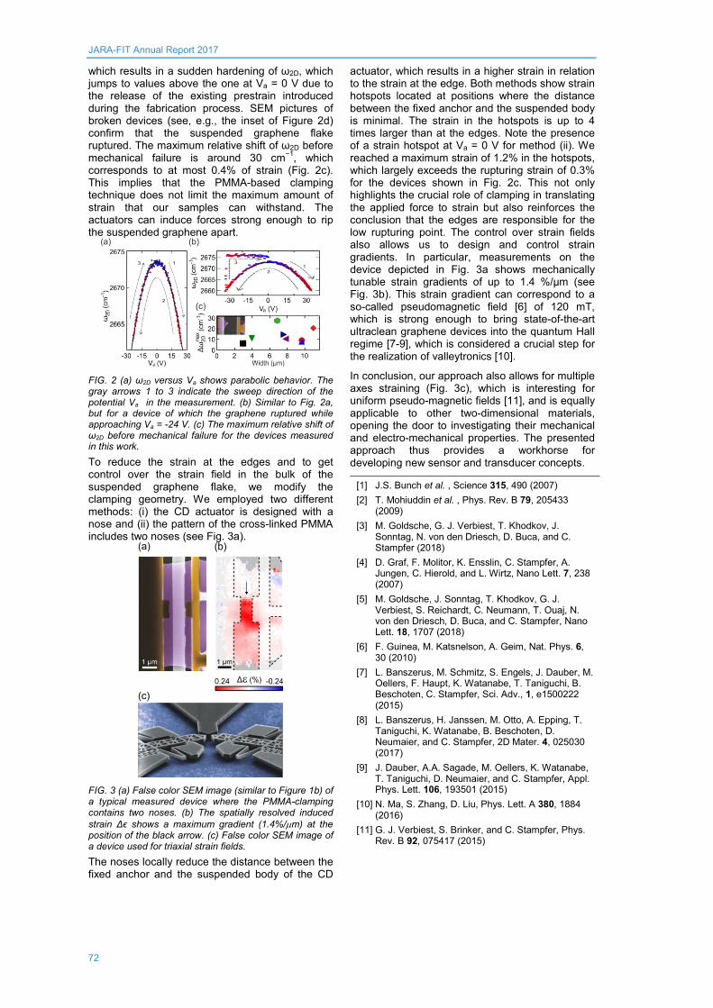
JARA-FIT Annual Report 2017
72
which results in a sudden hardening of ω2D, which jumps to values above the one at Va = 0 V due to the release of the existing prestrain introduced during the fabrication process. SEM pictures of broken devices (see, e.g., the inset of Figure 2d) confirm that the suspended graphene flake ruptured. The maximum relative shift of ω2D before mechanical failure is around 30 cm−1, which corresponds to at most 0.4% of strain (Fig. 2c). This implies that the PMMA-based clamping technique does not limit the maximum amount of strain that our samples can withstand. The actuators can induce forces strong enough to rip the suspended graphene apart.
FIG. 2 (a) ω2D versus Va shows parabolic behavior. The gray arrows 1 to 3 indicate the sweep direction of the potential Va in the measurement. (b) Similar to Fig. 2a, but for a device of which the graphene ruptured while approaching Va = -24 V. (c) The maximum relative shift of ω2D before mechanical failure for the devices measured in this work.
To reduce the strain at the edges and to get control over the strain field in the bulk of the suspended graphene flake, we modify the clamping geometry. We employed two different methods: (i) the CD actuator is designed with a nose and (ii) the pattern of the cross-linked PMMA includes two noses (see Fig. 3a).
FIG. 3 (a) False color SEM image (similar to Figure 1b) of a typical measured device where the PMMA-clamping contains two noses. (b) The spatially resolved induced strain Δϵ shows a maximum gradient (1.4%/µm) at the position of the black arrow. (c) False color SEM image of a device used for triaxial strain fields. The noses locally reduce the distance between the fixed anchor and the suspended body of the CD
actuator, which results in a higher strain in relation to the strain at the edge. Both methods show strain hotspots located at positions where the distance between the fixed anchor and the suspended body is minimal. The strain in the hotspots is up to 4 times larger than at the edges. Note the presence of a strain hotspot at Va = 0 V for method (ii). We reached a maximum strain of 1.2% in the hotspots, which largely exceeds the rupturing strain of 0.3% for the devices shown in Fig. 2c. This not only highlights the crucial role of clamping in translating the applied force to strain but also reinforces the conclusion that the edges are responsible for the low rupturing point. The control over strain fields also allows us to design and control strain gradients. In particular, measurements on the device depicted in Fig. 3a shows mechanically tunable strain gradients of up to 1.4 %/μm (see Fig. 3b). This strain gradient can correspond to a so-called pseudomagnetic field [6] of 120 mT, which is strong enough to bring state-of-the-art ultraclean graphene devices into the quantum Hall regime [7-9], which is considered a crucial step for the realization of valleytronics [10].
In conclusion, our approach also allows for multiple axes straining (Fig. 3c), which is interesting for uniform pseudo-magnetic fields [11], and is equally applicable to other two-dimensional materials, opening the door to investigating their mechanical and electro-mechanical properties. The presented approach thus provides a workhorse for developing new sensor and transducer concepts.
[1] J.S. Bunch et al. , Science 315, 490 (2007) [2] T. Mohiuddin et al. , Phys. Rev. B 79, 205433
(2009) [3] M. Goldsche, G. J. Verbiest, T. Khodkov, J.
Sonntag, N. von den Driesch, D. Buca, and C. Stampfer (2018)
[4] D. Graf, F. Molitor, K. Ensslin, C. Stampfer, A. Jungen, C. Hierold, and L. Wirtz, Nano Lett. 7, 238 (2007)
[5] M. Goldsche, J. Sonntag, T. Khodkov, G. J. Verbiest, S. Reichardt, C. Neumann, T. Ouaj, N. von den Driesch, D. Buca, and C. Stampfer, Nano Lett. 18, 1707 (2018)
[6] F. Guinea, M. Katsnelson, A. Geim, Nat. Phys. 6, 30 (2010)
[7] L. Banszerus, M. Schmitz, S. Engels, J. Dauber, M. Oellers, F. Haupt, K. Watanabe, T. Taniguchi, B. Beschoten, C. Stampfer, Sci. Adv., 1, e1500222 (2015)
[8] L. Banszerus, H. Janssen, M. Otto, A. Epping, T. Taniguchi, K. Watanabe, B. Beschoten, D. Neumaier, and C. Stampfer, 2D Mater. 4, 025030 (2017)
[9] J. Dauber, A.A. Sagade, M. Oellers, K. Watanabe, T. Taniguchi, D. Neumaier, and C. Stampfer, Appl. Phys. Lett. 106, 193501 (2015)
[10] N. Ma, S. Zhang, D. Liu, Phys. Lett. A 380, 1884 (2016)
[11] G. J. Verbiest, S. Brinker, and C. Stampfer, Phys. Rev. B 92, 075417 (2015)

JARA-FIT Annual Report 2017
73
Nanosized conducting filaments formed by atomic-scale defects in redox-based resistive switching memories H. Du1,2, C.-L. Jia1,3, A. Koehl3, J. Barthel1,2, R. Dittmann3, R. Waser3,4, and J. Mayer1,2 1 Ernst Ruska-Centrum für Mikroskopie und Spektroskopie mit Elektronen, Forschungszentrum Jülich,
Germany 2 Gemeinschaftslabor für Elektronenmikroskopie, RWTH Aachen University, Germany 3 Peter Grünberg Institute, Forschungszentrum Jülich, Germany 4 Institut für Werkstoffe der Elektrotechnik (IWE 2), RWTH Aachen University, Germany Redox-based resistive switching phenomena are found in many metal oxides and hold great promise for applications in next-generation memories and neuromorphic computing systems. Such kind of resistive switching involves the formation and disruption of electrically conducting filaments through ion migration accompanied by local electrochemical redox reactions. Hence, the conducting filaments are the functional basis of the resistive switching. The underlying mechanism in the conducting filaments is often explained by point defects, but so far clear experimental evidence of such defects is missing. In this work, we apply STEM, monochromated EELS and EDX atomic-scale imaging techniques to quantitatively characterize nanosized conducting filaments in electroformed Au / Fe:SrTiO3 / Nb:SrTiO3 thin film devices, providing direct experimental evidence for the point defect nature of the conducting filaments. Redox-based resistive random-access memories (ReRAM) have attracted great attention in the recent years because of their superior properties over the Si-based Flash memory and their additional potential for applications in neuromorphic computing systems [1]. ReRAM relies on the switchable change in resistance of a metal-insulator-metal structure under externally applied electrical stimuli. An initial electroforming process or the first current voltage cycle presets the pristine device, which can subsequently be switched hysteretically between its conductive ON and less conductive OFF states. The resistive switching process involves the formation and disruption of electrically conducting filaments through the migration of ions along with local electrochemical redox reactions. Depending on the nature of the mobile ions, two distinct fundamental switching mechanisms, electrochemical metallization (ECM) and valence change (VC), have been proposed. The ECM mechanism is related to the generation and migration of metal cations originating from one of the metal electrodes. The VC mechanism, on the other hand, is related to oxygen anion mobility in
the insulator. The thin insulator film in a VC cell is typically a transition metal oxide such as TiO2 and SrTiO3. In these oxides the formation and disruption of electrically conducting filaments are widely explained by a redox process based on the migration of oxygen ions along with the formation of oxygen vacancies (O-vacancies) and reduced metal oxide phases. For both ECM and VC switching mechanisms, the conducting filaments are therefore the key elements. For the well-known prototype VC material SrTiO3, extended defects, such as one-dimensional dislocations and two-dimensional stacking faults, as well as secondary oxygen deficient phases, e.g. Sr2Ti6O13 / SrTi11O20 in polycrystalline films, have been associated with the conducting filaments. The defects essential to the conducting filaments formation and disruption are still under debate. On the basis of an ion migration mechanism resistive switching is necessarily caused by point defects, however, quantification of point defects on atomic scale in a realistic device remains a challenge. X-ray absorption spectroscopy (XAS) has been demonstrated to be a successful technique to explore the Ti valence change and O-vacancies. Nevertheless, by means of XAS it is hardly possible to visualize the local structural details of individual filaments on atomic scale due to the limit of the lateral resolution of the technique (~25 nm). So far clear experimental evidence of conducting filaments formed exclusively by point defects is missing. The question still remains as to whether point defects alone are sufficient for the formation of conducting filaments. Here we apply STEM, EELS and EDX imaging techniques to quantitatively characterize nanosized conducting filaments in electroformed Au / Fe:SrTiO3 / Nb:SrTiO3 thin film devices [2], providing direct experimental evidence for the point defect nature of the conducting filaments. Conducting filaments are identified by a high local concentration of trivalent titanium ions correlating to oxygen vacancies. A high concentration of strontium vacancies and significant lattice distortions also occur in the filaments. Despite a high concentration of defects in the filaments, their general SrTiO3 perovskite structure is essentially

JARA-FIT Annual Report 2017
74
preserved. First insights into the switching mechanism are deduced from a snapshot simultaneously showing multiple nanosized filaments in different evolutionary stages.
FIG. 1: (a) Scheme of the device, (b) Electroforming I-V curve, and (c) Annular bright-field STEM image simultaneously showing multiple conducting filaments with darker contrast than the matrix.
Conducting filaments were created by electrical forming on individual devices by a sweep to +5~V with a current compliance of 10 mA, through which the devices (Fig. 1a) were set into the ON-state. The current voltage curve of the electrical forming process is shown in Fig. 1b. The top Au electrode of the devices was delaminated and replaced by a Pt layer to protect the film from ion beam damage during the TEM sample preparation. The cross-sectional TEM specimens were cut by focused ion beam (FIB) milling across the regions where Ti3+ has been detected by XAS to include the filaments in the TEM samples. The as-cut samples with initial thickness of about 100~nm were stepwise thinned by Ar-ion beam milling at 500–900 V acceleration voltages and inspected by TEM alternatingly until the thickness decreased to about 25 nm. Fig. 1c shows an annular bright field (ABF) STEM image of the cross-section of an electroformed device. We observed V-shaped areas showing darker contrast compared with their surroundings in the ABF image, providing a first indication that these areas are conducting filaments viewed in cross-section. Monochromated EELS spectrum imaging was performed from the region which is shown in Fig. 1c. Two constituent spectra showing distinctly different features of the O-K and Ti-L2,3 edges (Fig. 2a and 2b) were identified from the experimental spectrum data cube by multivariate data analysis using a joint Bayesian algorithm. The algorithm relies on the assumption that each acquired spectrum is a linear combination of constituent spectra plus additive noise. On the basis of the fraction maps, one constituent spectrum is attributed to the normal film matrix and substrate, while the other is ascribed to the defect V-shaped areas. The changes in the fine structures of the O-K (O 1s → 2p) and Ti-L2,3 (Ti 2p → 3d) edges present evidence for a high concentration of O-vacancies and Ti3+ in the V-shaped areas, and hence prove the related areas to be conducting filaments in the device.
FIG. 2: Electron core-loss spectra of (a) O-K edge and (b) Ti-L2,3 edge from normal SrTiO3 and conducting filaments comprising Ti3+. (c) Distribution map of Ti3+ (atomic percentage).
By a linear interpolation from a decrease in crystal-field splitting of the Ti-L2,3 edge about 20 % for 50 at% Ti3+ concentration reported in literature, the maximum Ti3+ concentration in the defect areas observed here is estimated to be 30 at%. This value was used to calibrate the fraction map of the corresponding constituent spectrum thereby transforming it into a Ti3+ distribution map (Fig. 2c). The Ti3+ distribution map clearly reveals four different V-shaped defect areas in the film developed to different stages (Fig. 2c). The shape of the filaments can be explained by the electric field and chemical gradients driving ion drift and chemical diffusion, respectively. Quantitative EDX analysis indicates also considerable Sr- and O-vacancies in the filaments. By taking both Sr-deficiency and static lattice distortion into account, multislice STEM image simulations can qualitatively reproduce the decrease of mean intensity in both ABF and high angle annular dark-field (HAADF) images of the filaments [2]. Intriguingly, atomic resolution STEM imaging reveals that the perovskite lattice is maintained intact at such high defect concentrations and considerable lattice distortions
In conclusion, our work [2], for the first time, provides clear experimental evidence for the existence of multiple nanosized conducting filaments formed solely by atomic-scale point defects in a SrTiO3 based thin film device. The coexistence of a high Ti3+ concentration along with Sr- and O-vacancies in the conducting filaments provides atomic scale explanations for the resistive switching mechanisms. The results shed light on the complexity of the conducting filaments formation that cation and anion defects need to be considered jointly. The presence of multiple nanosized conducting filaments in a single device may provide a mechanism for multi-level resistive switching.
We acknowledge the financial support by the Deutsche Forschungsgemeinschaft, SFB 917 Nanoswitches.
[1] R. Waser, R. Dittmann, G. Staikov, and K. Szot, Adv. Mate. 21, 2631 (2009).
[2] H. Du, C.-L. Jia, A. Koehl, J. Barthel, R. Dittmann, R. Waser, and J. Mayer, Chem. Mater. 29, 3164 (2017).

JARA-FIT Annual Report 2017
75
Direct visualization of GeTe-Sb2Te3 superlattice defects A. Meledin1,2, M. Kaminski3, M. Pohlmann3, M. Wuttig3,4, and J. Mayer1,2 1 Central Facility for Electron Microscopy, RWTH Aachen University, Germany 2 Ernst Ruska-Centre for Microscopy and Spectroscopy with Electrons, Forschungszentrum Jülich GmbH,
Germany 3 I. Institute of Physics, Physics of Novel Materials, RWTH Aachen University, Germany 4 JARA-Institute Energy-efficient Information Technology (Green IT), Forschungszentrum Jülich, Germany GeTe-Sb2Te3 superlattices (SLs) prepared by MBE were investigated by TEM. The seed Sb2Te3 layer as well as individual SL layers are not perfectly flat and contain twin domains. The SLs layers are chemically intermixed with each other, forming additional phases. The presence of all these defects leads to the multiple lattice distortions in the SL film, leading to dislocation formation in the most distorted regions.
The Ge-Sb-Te alloys are widely used in optical storage devices and in non-volatile PCRAM memory [1, 2, 3]. The interfacial phase change memory (iPCM) based on GeTe-Sb2Te3 SLs has recently attracted a lot of interest due to the lower power consumption in PC-RAM devices [4].
The defects in Sb2Te3 have been studied for many years [5]. A detailed description of the pulsed laser deposited (PLD) GeTe-Sb2Te3 superlattice micro- and nano-structure has been presented by Lotnyk at al [6]. In current work using Transmission Electron microscopy (TEM) we explore features of GeTe-Sb2Te3 SLs prepared by molecular beam epitaxy (MBE), therefore we will skip some of the previously described defects. MBE growth method allows precise control of layer thickness down to the atomic scale and results in higher quality structures.
The thin films were deposited by MBE at the Nanocluster in Forschungszentrum Jülich. An Sb2Te3 seed layer was deposited on Si(111) substrates followed by 10 layers of GeTe-Sb2Te3 grown on top of the seed layer. The substrate, a Si(111)-oriented wafer, was prepared in few steps. Firstly, it was chemically cleaned. Secondly, it was thermally treated to form Si(111)-7x7 reconstruction and finally the surface was Sb-passivated [7].
Cross-sectional lamellae for TEM were prepared by Focused Ion Beam (FIB) technique. Before the TEM investigation lamellae were shortly plasma-cleaned in Ar-O atmosphere to remove residual organic surface contamination.
High resolution high angle annular dark field scanning transmission electron microscopy (HAADF STEM) was performed using a probe Cs-corrected FEI Titan TEM, operated at 200kV and 300kV. Figure 1a contains a Z-contrast HAADF STEM image showing the overview of as-grown GeTe-Sb2Te3 based SL.
FIG. 1: Z-contrast HAADF STEM images showing a) an overview of the GeTe-Sb2Te3 superlattice with Sb2Te3 seed layer on Si substrate and b) the twin boundary in the Sb2Te3 seed layer.
The dark contrast area at the bottom corresponds to the low-Z Si substrate. The bright contrast layer, above the Si substrate, is the pure Sb2Te3 seed layer. On top of this layer there are 20 thin dark and bright contrast layers. The darker regions correspond to Ge-rich phase (lower Z), while brighter areas correspond to Sb-rich phase
a)
b)
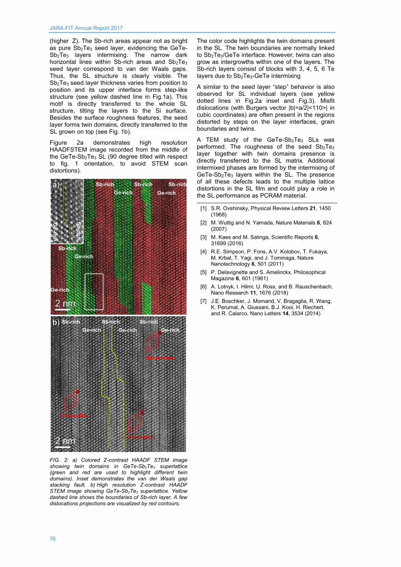
JARA-FIT Annual Report 2017
76
(higher Z). The Sb-rich areas appear not as bright as pure Sb2Te3 seed layer, evidencing the GeTe-Sb2Te3 layers intermixing. The narrow dark horizontal lines within Sb-rich areas and Sb2Te3 seed layer correspond to van der Waals gaps. Thus, the SL structure is clearly visible. The Sb2Te3 seed layer thickness varies from position to position and its upper interface forms step-like structure (see yellow dashed line in Fig.1a). This motif is directly transferred to the whole SL structure, tilting the layers to the Si surface. Besides the surface roughness features, the seed layer forms twin domains, directly transferred to the SL grown on top (see Fig. 1b).
Figure 2a demonstrates high resolution HAADFSTEM image recorded from the middle of the GeTe-Sb2Te3 SL (90 degree tilted with respect to fig. 1 orientation, to avoid STEM scan distortions).
FIG. 2: a) Colored Z-contrast HAADF STEM image showing twin domains in GeTe-Sb2Te3 superlattice (green and red are used to highlight different twin domains). Inset demonstrates the van der Waals gap stacking fault. b) High resolution Z-contrast HAADF STEM image showing GeTe-Sb2Te3 superlattice. Yellow dashed line shows the boundaries of Sb-rich layer. A few dislocations projections are visualized by red contours.
The color code highlights the twin domains present in the SL. The twin boundaries are normally linked to Sb2Te3/GeTe interface. However, twins can also grow as intergrowths within one of the layers. The Sb-rich layers consist of blocks with 3, 4, 5, 6 Te layers due to Sb2Te3-GeTe intermixing
A similar to the seed layer “step” behavior is also observed for SL individual layers (see yellow dotted lines in Fig.2a inset and Fig.3). Misfit dislocations (with Burgers vector |b|=a/2|<110>| in cubic coordinates) are often present in the regions distorted by steps on the layer interfaces, grain boundaries and twins.
A TEM study of the GeTe-Sb2Te3 SLs was performed. The roughness of the seed Sb2Te3 layer together with twin domains presence is directly transferred to the SL matrix. Additional intermixed phases are formed by the intermixing of GeTe-Sb2Te3 layers within the SL. The presence of all these defects leads to the multiple lattice distortions in the SL film and could play a role in the SL performance as PCRAM material.
[1] S.R. Ovshinsky, Physical Review Letters 21, 1450 (1968)
[2] M. Wuttig and N. Yamada, Nature Materials 6, 824 (2007)
[3] M. Kaes and M. Salinga, Scientific Reports 6, 31699 (2016)
[4] R.E. Simpson, P. Fons, A.V. Kolobov, T. Fukaya, M. Krbal, T. Yagi, and J. Tominaga, Nature Nanotechnology 6, 501 (2011)
[5] P. Delavignette and S. Amelinckx, Philosophical Magazine 6, 601 (1961)
[6] A. Lotnyk, I. Hilmi, U. Ross, and B. Rauschenbach, Nano Research 11, 1676 (2018)
[7] J.E. Boschker, J. Momand, V. Bragaglia, R. Wang, K. Perumal, A. Giussani, B.J. Kooi, H. Riechert, and R. Calarco, Nano Letters 14, 3534 (2014)

JARA-FIT Annual Report 2017
77
Vertex parametrization for the constrained functional renormalization group Carsten Honerkamp
Institute for Theoretical Solid State Physics, RWTH Aachen University, Germany
We present an efficient approximation for the low-energy effective electron-electron interaction in multiband lattice systems. This allows us to perform the constrained functional renormalization group (cfRG) with a suitable momentum and frequency discretization. We compute the effective interactions in the low-energy target band of a three-band model with onsite and non-local bare interactions. We show that the cfRG adds important features to the target-band interaction that cannot be found using the constrained random phase approximation (cRPA). The constrained random phase approximation (cRPA) [1–4] has become a widely used approach for the effective interaction in low-energy models for electrons in solids. Starting with a band structure on a wider energy scale, it al lows one to take into account efficiently the screening of the interactions that act in the low-energy window by the electrons in the bands outside this window. As expressed by its naming, the cRPA is an approximate scheme, perturbative in the electron-electron interactions, that consists in selecting a certain class of diagrams. It amounts to an infinite-order summation of a polarization function. The constraint consists in disallowing contributions to this polarization that are purely due to the low-energy bands (also called target bands).
For the cRPA is may be valuable to know whether there are relevant corrections terms. In previous works [5,6], we proposed to use a constrained functional renormalization group scheme (cfRG) to extend the cRPA and hence to include additional diagrams that are neglected in the cRPA into the calculation of the effective interactions (see Fig. 1, right side). The cfRG is an adaptation of the general functional renormalization group framework for interacting fermions [7] to the problem of tailoring effective target-band actions by integrating over the high-energy bands in multiband electron systems. We showed that at least in simple models [6], sizable corrections to cRPA can exist (but do not have to - this depends on the model). However, the frequency and momentum dependencies become quite rich in the cfRG, as the effective interaction of a translationally symmetric model depends on three momenta and three frequencies, in addition to four band or orbital indices. Therefore the cfRG-treatment of more realistic models that embody more definite material properties is facing a
bottleneck of how this wealth of infor- mation can be processed and evaluated efficiently.
In a new work (see Ref. [8] for details) we use the channel- decomposed cfRG for the computation of the effective in teractions in a low-energy target band of a generic three- band model (see Fig. 1 for a plot of the band structure) when the two bands away from the Fermi level are integrated out. We describe the interaction as the nonlocal and orbital-dependent coupling of particle-hole and particle-particle bilinears formed by fields residing in the same one or two orbitals.
FIG. 1: Left: Band structure of the three-orbital model described. The band in the middle is the target band for which the effective interaction is computed. The two outer bands are integrated out in cRPA or cfRG. Right: 5 one-loop dia- grams in the cfRG, with their physical meaning annotated. The cRPA sums only one of these diagrams. Besides restricting the momentum dependence to local bilinears, we also choose, in a first scheme, to concentrate on the orbital-diagonal, i.e. intraorbital bilinears. This approximation is called ’IOBI’ for intraorbital bilinears. The bare interaction can also be expressed with these bilinears. In a second, more general scheme, called two-orbital approximation, we check this assumption and take into account all two- particle interactions that only involve two orbital indices. Here we show results for the effective interactions and for the screening functions in these two approximations. In Fig. 2 we show data for pure intraorbital onsite interactions, with 𝑈 = 6,𝑈′ =0, 𝐽 = 0,𝑉𝑐 = 0. In the upper left plot we show the spatial dependence of the charge interaction for the bare case, the cRPA and the cfRG. The cfRG values in the upper plots are the ones from the two-orbital approximation. Even the bare interaction has acquired non-local contributions because the orbital-to-band transformation is momentum-dependent. The charge onsite term is significantly reduced by the cRPA compared to the bare value, but only slightly by the cfRG. In contrast with this, the cRPA produces an enhanced nearest neighbor repulsion, while the

JARA-FIT Annual Report 2017
78
cfRG lowers the nearest-neighbor repulsion compared to the bare interaction. Similar differences are observed for the effect tive spin interaction. Notably, the spin nearest-neighbor term in cfRG is repulsive, favoring antiferromagnetic alignment. This generation of nonlocal AF couplings was already observed [6].
FIG. 2: Effective target band interactions obtained with cRPA and cfRG, for onsite bare interactions 𝑈 = 6,𝑈′ = 0, 𝐽 = 0,𝑉𝑐 = 0. Upper plots: real space dependence of the effective interactions along the x-direction on the real lattice (charge channel in left plot, spin channel in right plot). Lower plots: static screening functions in the target band in the charge (left) and spin (right) channel as function of the wavevector along the Brillouin zone diagonal. The plots a) and b) in the upper half are for the two-orbital approximation. In the lower plots c) and d) we compare the IOBI approximation, denoted as cfRG(3), with the more general two-orbital cfRG. For the charge channel the curves lie on top of each other in this case.
In the lower panels of Fig. 2 we plot the target-band screening functions in charge and spin channels. Now we also compare the data for the IOBI approximation with that of the two-orbital approximation. For the pure intraorbital onsite repulsion the two-orbital approximation (thick lines) does not change the results of the IOBI (thin lines, if visible). The different spatial variation of the effective interactions in cRPA and both cfRG versions leads to quite different momentum dependencies of the static screening functions 𝜖𝑐ℎ 𝑠𝑠⁄ (). Most notably, the charge screening in cRPA is far stronger than in cfRG for half of the Brillouin zone at larger in line with the differences at small distances in the upper panel. Also, the spin screening function in the cfRG gets smaller than 1 for large 𝑞𝑥 = 𝑞𝑦 → 𝜋, i.e. there we have an enhancement of a staggered interaction component which can be found as well in the distance dependence of the real-space spin interaction in the panel above.
Similar differences exist for a longer-ranged bare interaction. In Fig. 3 we show the same set of data for interac tion parameters that include a density-density repulsion with decay length of 6 lattice sites.
FIG. 3.: Same as in Fig.2 with interaction paramters 𝑈 = 6,𝑈′ = 2, 𝐽 = 0,𝑉𝑐 = 2. Vc measures the strength of a bare Coulomb interaction with screening length of 6 lattice spacings.
Now the target-band onsite charge interaction in cfRG is even larger than the bare one, while the cRPA screens it down. For both cases, the spin interaction is positive on the nearest neighbor site again. The most striking difference is found in the dielectric or charge screening function where 𝜖𝑐ℎ() now becomes smaller than 1 in the cfRG for larger while is rises above 1 for the cRPA. Hence there is significant charge anti-screening for wavevectors near (𝜋,𝜋). The spin screening function dives below 1 as well for → (𝜋,𝜋) in Fig. 3.
Hence, the cfRG static screening properties can be quite different from those in cRPA, at least at small distances of the order of one lattice spacing. Considering the numerical effort, the IOBI or two-orbital approximations with one-frequency parametrization of the frequency de pendence should be on the same scale as cRPA. Therefore, we hope that additional improvements will be feasible and extensions to models with many bands, as may be required in first-principles theory, should become realistic.
The German Research Foundation supported this project via Ho2422/10-1, Ho2422/11-1 and the DFG Research Training Group 1995.
[1] F. Aryasetiawan, M. Imada, A. Georges, G. Kotliar, S. Bier- mann, and A. I. Lichtenstein, Phys. Rev. B 70, 195104 (2004)
[2] T. Miyake, F. Aryasetiawan, and M. Imada, Phys. Rev. B 80, 155134 (2009)
[3] M. Imada and T. Miyake, Journal of the Physical Society of Japan 79, 112001 (2010)
[4] E. Şaşıoğlu, C. Friedrich, and S. Blügel, Phys. Rev. B 83,121101 (2011)
[5] C. Honerkamp, Phys. Rev. B 85, 195129 (2012) [6] M. Kinza and C. Honerkamp, Phys. Rev. B 92,
045113 (2015) [7] W. Metzner, M. Salmhofer, C. Honerkamp, V.
Meden, and K. Schonhammer, Rev. Mod. Phys. 84 (2012)
[8] C. Honerkamp, ArXiv e-prints (2018), arXiv:1805.01669 [cond-mat.str-el]

JARA-FIT Annual Report 2017
79
Viability and challenges of low–temperature control electronics for spin qubits L. Geck1 , A. Kruth1, and H. Bluhm2 1 Central Institute ZEA-2, Electronic Systems, Forschungszentrum Jülich, Germany 2 JARA-FIT Institute Quantum Information, Forschungszentrum Jülich and RWTH Aachen Univer sity,
Germany Quantum computers hold the promise to solve efficiently certain problems that are intractable for classical computers, by using quantum algorithms that exploit fundamental quantum phenomena such are superposition and entanglement [1]. However, to solve practically relevant problems (e.g. factorizing large numbers) a quantum computer would require millions of physical quantum bits or qubits [2]. Current demonstra- tors typically range from a few to a few tens of qubits [3, 4], and scaling up these systems to the size needed for running a full quantum algorithm remains an open daunting task. One aspect that is receiving increasing attention is the scalability of the the (classical) control infrastructure used to manipulate and read–out the qubits. An attractive approach is to develop a customized, highly integrated control system, to be placed at low temperature in the immediate vicinity of the qubits. Here we analyze critically the viability of such an approach, taking as reference the phys- ical requirements of a two-electron spin qubit, and the specifications of a standard commercial 65nm CMOS technology.
A full-blown quantum computer will likely count mil- lions if not billions of qubits. This large number mainly comes from the need of making quantum systems robust against errors due to decoherence, i.e. against the loss of the information stored in the qubits due to the interaction with the environment. This type of errors can be counteracted by redundantly encond- ing of the fragile quantum information to enable er ror correction, but this impose an overhead of 102 to 105 in the number of qubits. Connecting and controlling such a large number of qubits, represents a formidable engineering challange. Current experiments employ room temperature signal generators, whose output is routed via coaxial cables down to the cryostats hosting the qubits, which are operated at temperatures of 20-100 mK. This approach will become however very cumbersome beyond a few hundred qubits at the latest, and seems completely impractical for the large numbers eventually required [5]. For example, 106 UT-34 coaxial cables with a diameter of 0.9 mm2 each correspond to a total cross section of 0.6 m2. Such cabling would impose an unacceptable heat load on the cryogenic end,
and cannot be connected directly to highly integrated qubit chips – current semiconductor technology is limited to die–sizes of about 30 mm. This and other problems related to the use to room-temperature control electronics (e.g. the huge power consumption, which is currently around 1kW per qubit) could be addressed with purpose–built, highly integrated circuits operating at low temperature in the immediate vicinity of the qubits, either on the same chip or with some form of chip-to-chip bonding. Ideally, each qubit would be associated with a control unit provid- ing the required read-out and control functionalities unit, with a footprint corresponding to the average
FIG. 1: a) Block diagram of the control electronics for one qubit. b) Structure of two registers of bias memory with four–bit resolution.
a)
b)
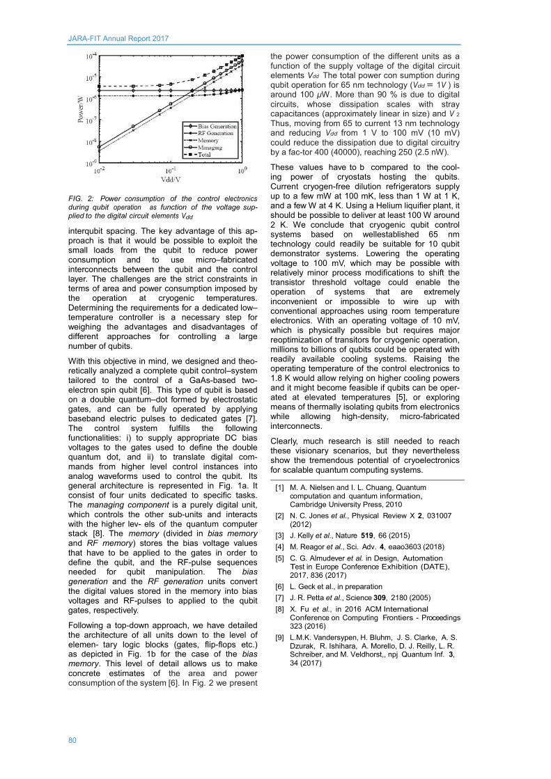
JARA-FIT Annual Report 2017
80
FIG. 2: Power consumption of the control electronics during qubit operation as function of the voltage sup- plied to the digital circuit elements Vdd
interqubit spacing. The key advantage of this ap- proach is that it would be possible to exploit the small loads from the qubit to reduce power consumption and to use micro–fabricated interconnects between the qubit and the control layer. The challenges are the strict constraints in terms of area and power consumption imposed by the operation at cryogenic temperatures. Determining the requirements for a dedicated low–temperature controller is a necessary step for weighing the advantages and disadvantages of different approaches for controlling a large number of qubits.
With this objective in mind, we designed and theo- retically analyzed a complete qubit control–system tailored to the control of a GaAs-based two-electron spin qubit [6]. This type of qubit is based on a double quantum–dot formed by electrostatic gates, and can be fully operated by applying baseband electric pulses to dedicated gates [7]. The control system fulfills the following functionalities: i) to supply appropriate DC bias voltages to the gates used to define the double quantum dot, and ii) to translate digital com- mands from higher level control instances into analog waveforms used to control the qubit. Its general architecture is represented in Fig. 1a. It consist of four units dedicated to specific tasks. The managing component is a purely digital unit, which controls the other sub-units and interacts with the higher lev- els of the quantum computer stack [8]. The memory (divided in bias memory and RF memory) stores the bias voltage values that have to be applied to the gates in order to define the qubit, and the RF-pulse sequences needed for qubit manipulation. The bias generation and the RF generation units convert the digital values stored in the memory into bias voltages and RF-pulses to applied to the qubit gates, respectively.
Following a top-down approach, we have detailed the architecture of all units down to the level of elemen- tary logic blocks (gates, flip-flops etc.) as depicted in Fig. 1b for the case of the bias memory. This level of detail allows us to make concrete estimates of the area and power consumption of the system [6]. In Fig. 2 we present
the power consumption of the different units as a function of the supply voltage of the digital circuit elements Vdd The total power con sumption during qubit operation for 65 nm technology (Vdd = 1V ) is around 100 µW. More than 90 % is due to digital circuits, whose dissipation scales with stray capacitances (approximately linear in size) and V 2
Thus, moving from 65 to current 13 nm technology and reducing Vdd from 1 V to 100 mV (10 mV) could reduce the dissipation due to digital circuitry by a fac-tor 400 (40000), reaching 250 (2.5 nW).
These values have to b compared to the cool- ing power of cryostats hosting the qubits. Current cryogen-free dilution refrigerators supply up to a few mW at 100 mK, less than 1 W at 1 K, and a few W at 4 K. Using a Helium liquifier plant, it should be possible to deliver at least 100 W around 2 K. We conclude that cryogenic qubit control systems based on wellestablished 65 nm technology could readily be suitable for 10 qubit demonstrator systems. Lowering the operating voltage to 100 mV, which may be possible with relatively minor process modifications to shift the transistor threshold voltage could enable the operation of systems that are extremely inconvenient or impossible to wire up with conventional approaches using room temperature electronics. With an operating voltage of 10 mV, which is physically possible but requires major reoptimization of transitors for cryogenic operation, millions to billions of qubits could be operated with readily available cooling systems. Raising the operating temperature of the control electronics to 1.8 K would allow relying on higher cooling powers and it might become feasible if qubits can be oper- ated at elevated temperatures [5], or exploring means of thermally isolating qubits from electronics while allowing high-density, micro-fabricated interconnects.
Clearly, much research is still needed to reach these visionary scenarios, but they nevertheless show the tremendous potential of cryoelectronics for scalable quantum computing systems.
[1] M. A. Nielsen and I. L. Chuang, Quantum computation and quantum information, Cambridge University Press, 2010
[2] N. C. Jones et al., Physical Review X 2, 031007 (2012)
[3] J. Kelly et al., Nature 519, 66 (2015) [4] M. Reagor et al., Sci. Adv. 4, eaao3603 (2018) [5] C. G. Almudever et al. in Design, Automation
Test in Europe Conference Exhibition (DATE), 2017, 836 (2017)
[6] L. Geck et al., in preparation [7] J. R. Petta et al., Science 309, 2180 (2005) [8] X. Fu et al., in 2016 ACM International
Conference on Computing Frontiers - Proceedings 323 (2016)
[9] L.M.K. Vandersypen, H. Bluhm, J. S. Clarke, A. S. Dzurak, R. Ishihara, A. Morello, D. J. Reilly, L. R. Schreiber, and M. Veldhorst,, npj Quantum Inf. 3, 34 (2017)

JARA-FIT Annual Report 2017
81
Transferring a quantum state from a photonic qubit to a gate–defined quantum dot B. Joecker1, Pascal Cerfontaine1, L. Schreiber1, B. Kardynal2, and H. Bluhm1
1 JARA-FIT Institute Quantum Information, Forschungszentrum Jülich and RWTH Aachen University, Germany
2 Peter Grünberg Institut-9, Forschungszentrum Jülich, Germany Interconnecting well–functioning, scalable sta- tionary qubits and photonic qubits could sub- stantially advance quantum communication applications and serve to link future quantum processors. We considered two protocols for transferring the state of a photonic qubit to a single–spin and to a two–spin qubit hosted in gatedefined quantum dots (GDQD). Both protocols are based on using a localized exciton as intermediary between the photonic and the spin qubit. Using effective models to describe the hybrid systems formed by the the exciton and the GDQDs, and applying simple but realistic noise models to analyze the viability of the proposed protocols, we find that they can be completed with a success probability around 90%.
Spin qubits based on GDQD in GaAs/AlxGa1-xAs heterostructures have pioneered the field of quantum information processing by demonstrating all key requirements such as qubit initialization and readout [1], coherent control [2] and two-qubit gates [3]. Moreover, thanks to their similarity to the transistors used in modern computer chips, these top–down fabricated quantum dots have good prospects for realizing large scale quantum processing nodes. However, GDQDs pose a number of challenges when it comes to couple them coherently with light. The problems come from the lack of exciton confinement: while electron states are confined in GDQD, hole states are not. Since in the creation of an exciton the spin of the photo–excited electron is always entangled with the one of the hole, discarding the hole spin inevitably leads to decoherence of the electron spin. This limits considerably the possibility of optically controlling and manipulating spins in GDQDs, and it hinders their applicability in quantum communications. Despite these difficulties, the coherent coupling of photons and spins in GDQDs is an active area of research [4], motivated by the fact that robust spin–photon entanglement is a key requirement for quantum repeaters for long-distance quantum communi- cations [5] as well as for distributed quantum com- puting [6].
We propose using a self–assembled quantum dot (SAQD) as interface between a photonic qubit and a spin qubit in a GDQD. Unlike GDQD, SAQD exhibit excellent optical control of the spin state,
including information transfer between spin and photons [7], but do not represent a scalable qubit model. Combining the strengths of these two systems might allow developing an optically addressable quantum processor. Based on this idea, we analyze the feasibility of two different information transfer protocols, using effective models to describe the hybrid system formed by a bound exciton in the SAQD tunnel coupled to a GDQD.
In the first protocol, we consider the case where the quantum state of the photon is mapped onto the state of a single–spin qubit, as sketched in Fig. 1b. The first step of the protocol is the photoexcitation of an exciton in the SAQD in the Voigt configuration, i.e. in the presence of a strong in-plane magnetic field, which makes all exciton states |↓Ý)x , |↑ß)x , |↑Ý)x , |↓ß)x optically addressable.
FIG. 1: a) Schematic of a GaAs/AlGaAs heterostructure hosting a hybrid device formed by a double quantum–dot tonnel defined by metallic top-gates, which is coupled to a self-assembled quantum dot (red disc). b) Model of a single–level GDQD tunnel coupled to an optically active quantum dot. Here, tc represents the tunnel coupling between the GDQD and the SAQD, ε the energy detuning between the electronic level in the GDQD and in the exciton, and Hex the excitonic exchange interaction in the SAQD. c) Model of a double dot tunnel coupled to a SAQD.

JARA-FIT Annual Report 2017
82
Here, the simple arrow represents the spin state of the photo-excited electron and the double-arrow the one of the photo-excited hole in the SAQD. States with parallel spins can be addressed only with horizontally polarized photons, while eigenstates with antiparallel-spins require vertically polarized photons. The trick to avoid entanglement between electron and hole upon photon-excitation, is to encode information in a way that only involves excitonic-states with the same spin state for the hole, i.e. to map information as follow: ∝ |𝜔1, H) + 𝛽|𝜔2, V) → 𝛼|↑ Ý)𝑥 + 𝛽|↓ Ý)𝑥, where α and β are complex numbers and |𝜔, H(V)) represents a photon state with energy ω and horizontal (vertical) polarization. The next step of the information–transfer process is the adiabatic transfer of the photo–excited electron from the SAQD to the GDQD, 𝛼|° ↑ Ý)𝑥 + 𝛽|° ↓ Ý)𝑥 →𝛼|↑ °Ý)𝑥 + 𝛽|↓ ° Ý)𝑥, where now ° represents an empty electronic state. This can be achieved by tunnel coupling the electron state in the SAQD to a GDQD and by tuning the detuning E between the SAQD and the GDQD (see Fig. 1b), in such a way that it becomes energetically favorable for the electron to occupy the GDQD.
The accuracy of this adiabatic transfer process determines the ultimate viability of the transfer protocol. The first source of errors affecting the adiabatic transfer are non-adiabatic transitions to other states, which can occur if the detuning ε is increased too quickly. Maintaining the probability of non adiabatic transitions below 1% poses an upper limit to the sweep speed vE , which in turn determines the time on which the transfer can be complete. On this timescale, the system is subject to radiative recombination – which causes excitons to decay – and dephasing due to charge and nuclear-spin noise – which cause the loss of information. We take all these factors into account using simple effective models, and we evaluate the performance of the transfer protocol [8]. The results for a set of realistic parameters for the device specification and for the noise sources, are presented in Fig. 2. In this case, radiative recombination and dephasing (quantified by ⟨𝛿𝜑122 ⟩ only marginally limits the probability of a successful transfer, indicating the feasibility of the protocol.
This approach can be extended to transfer infor- mation to a singlet–triplet qubit encoded in a gate- defined double quantum-dot (DD), see Fig. 1c. The advantage of this set-up is that singlet–triplet qubits allow high manipulation fidelities in systems with large hyperfine interaction such as GaAs [2]. However, it is more involved than in the case of the single-spin qubit and, in addition to the steps described above (photo-excitation and adiabatic transfer), it also require a) the initialization of one electron in the double dot and, b) the application of a suitable Rabi pulse to map the transferred state into the chosen computational space [8]. Using
again effective models to describe the system and the main sources of errors, we find that also in this case the information transfer protocol can be completed with a success probability around 90%.
FIG. 2: Performance of the protocol for transferring information to a single spin qubits, for a set of realistic parameters for GaAS-based devices. a) Probability that no optical–recombination occurs during the adiabatic transfer along the branches |° ↑ Ý) → |↑ °Ý) (red) and |° ↓ Ý) → |↓ °Ý) (blue). b) Dephasing due to different noise sources during the adiabatic transfer. The final values are displayed on the right. t is the time elapsed from the beginning of the protocol, with the largest value shown corresponding to its completion.
Our results are based on conservative estimates of the device parameter and leave substantial room for improvements. Nevertheless, they already clearly indicate that the proposed schemes could be implemented with reasonably high success probability.
[1] J. M. Elzerman et al.,Nature 430, 431 (2004), C. Barthel et al., Phys. Rev. Lett. 103, 160503 (2009)
[2] F. H. Koppens, et al.,Nature 442, 766 (2006), S. Foletti et al., Nature Phys. 5, 903 (2009), P. Cerfontaine et al., Phys. Rev. Lett. 113,150501 (2014)
[3] K. C. Nowack et al.,Science 333, 1269 (2011), M. Shulman et al., Science 336, 202 (2012)
[4] H. Kosaka et al., J. Appl. Phys. 109, 102414 (2011), T. Fujita et al., Phys. Rev. Lett. 110, 266803 (2013)
[5] W. Dür et al., Phys. Rev. A, 59, 169 (1999) [6] R. Van Meter et al., Distributed Arithmetic on a
Quantum Multicomputer, Vol. 34 (IEEE Computer Society, 2006)
[7] D. Press et al., Nature 456, 218 (2008), K. De Greve et al., Nature 491, 421 (2012), W. B. Gao, Nature 491, 426 (2012)
[8] B. Joecker et al., in preparation (2018)

JARA-FIT Annual Report 2017
83
Strain relaxation and ambipolar electrical transport in GaAs/InSb core-shell nanowires P. Zellekens1, T. Rieger1, N. Demarina2, A. al Hassan3, F. J. Hackemüller1, U. Pietsch3, T. Schäpers1, D. Grützmacher1, and M. I. Lepsa1 1 Peter Grünberg Institut-9, Forschungszentrum Jülich, Germany 2 Peter Grünberg Institut-2, Forschungszentrum Jülich, Germany 3 Universität Siegen, Festkörperphysik, 57068 Siegen, Germany The growth, crystal structure, strain relaxation mechanisms and room temperature transport characteristics of GaAs/InSb core/shell nanowires are investigated. A combination of different analysis techniques, i.e. scanning electron microscopy (SEM), high resolution transmission electron microscopy (HRTEM), geometric phase analysis (GPA) and x-ray diffraction (XRD) reveals, that these material systems can form stable, radial heterostructures despite the huge lattice mismatch of almost 14%. The lattice strain is thereby relaxed within 3nm around the interface of both materials. Room temperature field-effect measurements reveal an ambipolar behavior, a gate-tunable switch from electron to hole transport. The investigation of multiple wires with different core radii and shell thicknesses showed that there is also a strong size dependency, i.e. a thin shell leads to a more pronounced p-type behavior. Supporting band structure and conductance calculations reveal that this effect can be mainly attributed to a strong asymmetry between the band structure for electrons and holes.
Semiconductor nanowires, fabricated by a bottom-up approach, are promising as building blocks for future nanoscaled electronic devices. Furthermore, they are also interesting objects for studying fundamental quantum phenomena. For semiconductor nanowires mainly low band-gap materials such as InAs, or InSb are used. The underlying reason is that owing to the Fermi level pinning within the conduction band a surface accumulation layer is formed. This ensures conductance even for small nanowire radii. While InSb is an interesting material by itself due to its intriguing electronic properties, i.e. the highest electron mobility of all III/V semiconductors, its properties can be further improved for nanowires by adding a high band gap semiconductor as a core material. In the case of GaAs/InSb core/shell nanowires, the inner part behaves like an insulator, which effectively changes the topology of the electronic system to a geometry, which is quite similar to an Aharonov-Bohm ring [1]. Due to this effect, combined with the strong spin-orbit coupling, GaAs/InSb nanowires are possible components for devices to study quantum
interference or topological effects like Majorana excitations [2].
FIG. 1: Overview and zoomed-in SEM micrographs of GaAs/InSb core/shell nanowires with a shell growth time of 5min (a,d), 30min (b,e) and 90min (c,f).
The GaAs/InSb core/shell nanowires were grown by self-catalyzed molecular beam epitaxy on Si (111) substrates covered by a native SiO2 layer with pinholes. The latter ones act as nucleation centers for the catalyzing Ga droplet. After the formation of the GaAs core, the growth of the surrounding InSb shell is started. In order to get a smooth and conformal layer, the substrate temperature was set to values between 280°C and 320°C. Fig. 1 shows SEM micrographs of wires from three different growth runs. The growth times for the InSb shells were set to 5 (a,d), 30 (b,e) and 90 min (c,f). It can be clearly seen, that for the shortest growth duration the shell is incomplete and rough, which can be attributed both to the island-based growth as well as the huge lattice mismatch of almost 14%. For longer growth times, the roughness is reduced and a coalescent and smooth InSb shell is formed.
Large mismatches between two semiconductors induce a lot of strain inside the lattice and can potentially change the band structure and thereby the electronic properties of the whole structure.

JARA-FIT Annual Report 2017
84
FIG. 2(a,b): HRTEM images for different nucleation spots of InSb on GaAs, superimposed by GPA strain maps. All of them show an abrupt compensation of the lattice mismatch induced strain close to the interface.
However, it is already known, that nanowires can potentially compensate this strain by means of relaxation due to the formation of dislocations. To evaluate the strain relaxation, we used a combination of multiple analysis techniques like XRD and HRTEM. Fig. 2 (a,b) shows a superposition of HRTEM micrograph and GPA strain maps for the nucleation of InSb on the wurtzite phase of GaAs. All of them show an almost abrupt transition of the lattice spacing within 3nm around the interface. A detailed investigation reveal, that the relaxation is mainly driven by the creation of perfect dislocations, Frank partial dislocations and Shockley partial dislocations. Based on these findings, the electronic band structure of the nanowire can be considered as bulk-like [3].
FIG. 3: (a) Gate-dependent IV curves of a GaAs/InSb nanowire with a core radius of 40nm and a shell thickness of 9nm. (b) Transconductance curves of four wires with different shell thicknesses.
In order to probe the electronic properties, the wires were mechanically transferred to pre-patterned highly n-doped Si substrate capped by a 200nm thick SiO2 layer which acts as a gate dielectric. Prior to the deposition of Ti/Au contacts, the nanowires were cleaned in a 1:2 mixture of HCl:H2O in order to remove the native oxide. Fig.3 (a) shows a collection of gate-dependent IV curves for a wire with a core radius of 40nm and a shell thickness of 9nm. It can be clearly seen, that a more negative gate voltage leads to a steeper slope, i.e. an increase of the conductance. This is typical for a system with p-type behavior. However, while a more positive gate voltage first leads to a
reduction of the conductance, at some point the current flow starts to increase again. This so-called ambipolarity can be further tuned by the geometry of the wires. Fig. 3(b) shows the transconductance curves of wires obtained from four different growth runs with varying shell thicknesses. It can be seen, that although all of the wires show an ambipolar behavior, the dominating carrier type changes from p- to n-type if the shell thickness is increased.
FIG. 4: (a,b) Calculated band structures of a nanowire. (a) corresponds to a negative gate voltage, (b) shows the behavior for a positive gate voltage. (c) Calculated conductance of the same wires depicted in Fig. 3(b).
In order to theoretically explain the type of transport for different geometries, the band profile as well as the carrier occupation were calculated by a Schrödinger-Poisson solver. As can be seen in Fig 4(a), the calculations reveal that only the InSb shell is populated by charge carriers, whereas the GaAs core behaves like an insulator. In case of a negative gate voltage, as depicted in Fig. 4(a), the large effective mass of the holes leads to a strong increase in the number of carriers due to the huge number of states close to the valence band. However, for a more positive gate voltage (cf. in Fig. 4b), the number of electrons increases and the systems shows n-type behavior. Due to the smaller effective mass, the states close to the conduction band are much more influenced if the shell thickness is reduced. The confinement induced shift of the states leads to a pronounced p-type behavior, which is clearly visible in the calculated conductance curves depicted in Fig. 4(c).
In conclusion, it could be shown that GaAs/InSb core/shell nanowires can form strain-free heterostructures in which the electronic transport can switched from n- to p-type by means of an external gate voltage.
[1] Ö. Gül, N. Demarina, C. Blömers, T. Rieger, H. Lüth, M. I. Lepsa, D. Grützmacher, and Th. Schäpers, Phys. Rev. B 89, 045417 (2014)
[2] V. Mourik, K. Zuo, S. M. Frolov, S. R. Plissard, E. P. A. M. Bakkers, and L. P. Kouwenhoven, Science 336, 1003 (212)
[3] T. Rieger, P. Zellekens, N. Demarina, A. al Hassan, F.J. Hackemüller, H. Lüth, U. Pietsch, T. Schäpers, D. Grützmacher, and M. I. Lepsa, Nanoscale 9, 18392 (2017)

JARA-FIT Annual Report 2017
85
Surface space charge formation in donor doped SrTiO3 M. Andrä1, F.Dvořák2, M. Vorokhta2, S. Nemšák1, V. Matolín2, C. M. Schneider1, R. Dittmann1, F. Gunkel1,3, D. N. Mueller1, and R. Waser1,3 1 Peter Grünberg Institut-7, Forschungszentrum Jülich, Germany 2 Department of Surface and Plasma Science, MFF UK, Charles University, Prague, Czech Republic 3 Institute of Electronic Materials (IWE II), RWTH Aachen University, Germany Bulk n-SrTiO3 is mostly referred to as a degenerate n-type semiconductor. However, recent research on n-SrTiO3 indicated the existence of a surface space charge layer rendering its surface properties more complex: 1) Marchewka et al. [1] revealed the existence of an electron depletion layer in Pt/Fe:SrTiO3/Nb:SrTiO3 structures extending into the Nb-doped bottom electrode suggested to be acceptor-type interface defects. 2) These findings are complemented by Meyer et al. [2] who recently proposed a high temperature surface oxidation model that proposed electron depletion in the near surface region of n-SrTiO3 in oxidizing conditions with the incorporation of negatively charged surface VSr
'', accompanied by the precipitation of strontium oxide (SrO) at the surface. 3) In addition, Setvin et al. [3] showed the existence of oxygen molecules forming superoxides at TiO2 surfaces below 300 K. Thus, up to now, it is not known, whether possibly chemisorbed charged oxygen molecules such as observed for TiO2, or intrinsic ionic surface defects, namely VSr
'' , can cause the observed surface space charge layer effect in n-SrTiO3 and its dependence on the oxygen partial pressure (pO2).
In order to get further insight on the surface reaction and electrical properties of n-SrTiO3 directly, we used 0.5 w% Niobium doped SrTiO3 thin films homoepitaxially grown on undoped SrTiO3 substrates and analyzed them by in-situ near ambient pressure X-ray photoelectron spectroscopy at a temperature of 770 K and oxygen partial pressures up to 5 mbar. The sample stack and the measurement setup is schematically shown in Fig. 1. Fig. 2 shows the pO2-dependent core level spectra of O 1s and C 1s (a), Ti 2p and Sr 3d (c), as well as the valence band region (d) obtained at room temperature (dashed spectra) and at an elevated temperature of 770 K (solid spectra).
FIG. 1: Schematic illustration of the sample stack as well as the near ambient pressure X-ray photoelectron spectroscopy measurement setup.[3]
FIG. 2: Core level spectra of O1s and C1s (a), Ti2p (b) and Sr3d (c), as well as the valence band region (d) of a 32 nm thick Nb:SrTiO3 film at room temperature (dashed spectra) and 770 K (solid spectra).[3]
Initial spectra were taken at room temperature and UHV (dashed top spectra) on as-prepared samples. As can be seen from the O1s and the C1s spectra (FIG. 2a), a significant amount of carbon adsorbates and contaminants is present at the thin film surface resulting from exposure to air after the PLD growth process and ex-situ transfer into the NAP-XPS setup. Upon heating to 770 K in UHV, a reduction of the carbon adsorbates and contaminants is clearly visible in the O1s and the C1s spectra. Subsequently, the pO2 was increased stepwise from 0.05 mbar to 5 mbar while the temperature of 770 K was maintained. All carbon adsorbates and contaminants are removed from the surface upon heating at a pO2 above 0.05 mbar. With increasing pO2, a significant shift of up to 0.6 eV towards lower binding energies (BE) is detected for all the characteristic core level spectra and the valence band maximum (VBM). Full reversibility of the BE shifts was confirmed by a following set of spectra taken again in UHV

JARA-FIT Annual Report 2017
86
conditions at 770 K (solid circles to dashed circles), pointing towards a reversible underlying surface process, solely governed by the ambient pO2. Neither the small spectral differences in the O1s, the Sr3d, in the Ti2p, nor any spectral changes in the VB spectra allow for an unambiguous interpretation as chemical changes. In fact, any of two scenarios described above (chemisorbed charged oxygen molecules and/or SrO precipitation) may describe the changes in the peak shapes equally well.
Fig. 3 shows the BE values of the core levels (a), the difference between the Fermi energy (EF) and the valence band maximum as well as the estimated temperature dependent position of the conduction band minimum (CBM) (b), and the relative BE shift of the different core level spectra and the VBM with respect to the initial UHV measurements (c) at 770 K. The measured position of the difference between EF and the VBM at an absolute pressure of 10-8 mbar is close to the temperature dependent CBM expected at 770 K (FIG.3b, dashed line), indicating that the Fermi energy of the thin film is close to the conduction band as expected from classical semiconductors. The more the pO2 is increased the more the VBM is shifted towards lower BE, indicating a continuous shift of the Fermi energy deeper into the band gap. The relative shifts of the different core levels nearly overlap on a single line with the one of the VBM, indicating that all peaks shift rigidly with pO2 within the experimental uncertainty. In the rigid band model the apparent BE of the core levels is governed solely by the Fermi energy of the sample. Therefore it is a direct measure of the concentration of the surface electrons at the surface of the sample. Consequently, the measured rigid shift of all core level spectra of SrTiO3 and the VBM can be explained by a mere shift of the Fermi energy at the surface, i.e. an effective change of the conduction band filling.
Fig. 4 illustrates the relative positions of the Fermi energy in UHV conditions and 5 mbar pO2 at 770 K as indicated by the NAP-XPS results. In UHV, the position of the Fermi energy close to the conduction band suggests a bulk-like behavior of the n-SrTiO3 surface, with a constant carrier concentration over the entire thickness of the thin film. In contrast, at increased pO2, the observed relative shift of the Fermi energy into the band gap
indicates a reduction of the electron concentration in the n-SrTiO3 thin film, implying a negative surface charge that is reversibly controlled by varying the ambient oxygen atmosphere. Using a parabolic potential approach the potential profile and the corresponding electrostatic decay length
0d ( 2 ) / (eN)SCR re e= − Φ can be estimated to be
about 7nm at 5mbar O2. Hence, assuming a process limited to the surface it can be inferred that the electron concentration deep in the thin film is given by the niobium dopant concentration. The resulting electron concentration difference between the bulk and the surface of the thin film thus implies the formation of a surface space charge layer and with that, a band bending that can be controlled by varying the pO2. In summary, we investigated the electronic surface structure of donor-doped strontium titanate of homoepitaxial 0.5 wt% donor-doped SrTiO3 thin films by in-situ near ambient pressure X-ray photoelectron spectroscopy at a temperature of 770 K and oxygen pressures up to 5 mbar. Upon exposure to an oxygen atmosphere at elevated temperatures, we observed a rigid binding energy shift of up to 0.6 eV towards lower binding energies with respect to vacuum conditions for all SrTiO3 core level peaks and the valence band maximum with increasing oxygen pressure. The rigid shift is attributed to a relative shift of the Fermi energy towards the valence band concomitant with a negative charge accumulation at the surface, resulting in a compensating electron depletion layer in the near surface region. The negative surface charge may be provided by the formation of cation vacancies or the formation of charged oxygen adsorbates at the surface. Regardless of the process at the surface, our results clearly indicate a pO2-dependent surface space charge formation in donor-doped SrTiO3 in oxidizing conditions.[1]
The presence of such surface layers needs to considered for all devices based on Nb-STO and may contribute to the full understanding of band profiles at oxide/gas phase interfaces.
[1] Marchewka et. al., Scientific Reports 4, 6975 (2014)
[2] R. Meyer et. al., Phys. Rev. B 94, 115408 (2016)
[3] M. Setvin et al. Surf. Sci. 626, 61 (2014), M. Setvin et al., Science 341, 988 (2013)
[4] M. Andrä et. al., APL Materials 5, 056106 (2017)
FIG. 4: Schematic illustration of the relative positions of the Fermi energy in UHV conditions and 5 mbar pO2 at 770 K. The surface carrier concentration in the electronic.[4]
FIG. 3: Position of the characteristic BE of SrTiO3 core levels (a), the energy difference between the Fermi energy and the valence band maximum (b). BE shift relative to measurements in UHV conditions (c).[4]

JARA-FIT Annual Report 2017
87
Spectroscopic indications of tunnel barrier charging as the switching mechanism in memristive devices B. Arndt1, F. Borgatti2, F. Offi3, T. Meiners1, S. Menzel1, K. Skaja1, G. Panaccione4, R. Waser1,5, R. Dittmann1 1 Peter Grünberg Institut-7, Forschungszentrum Jülich, Germany 2 CNR – Istituto per lo Studio dei Materiali Nanostrutturati (ISMN), Bologna, Italy 3 CNISM and Dipartimento di Scienze, Rome, Italy 4 CNR – Istituto Offi cina dei Materiali (IOM), Laboratorio TASC, Trieste, Italy 5 Institute of Electronic Materials (IWE II), RWTH Aachen University, Germany Resistive random access memory is a promising, energy efficient, low power ‘storage class memory’ technology that has the potential to replace both flash storage and on-chip dynamic memory. Whilst the most widely employed systems exhibit filamentary resistive switching, interface type switching systems [1] based on a tunable tunnel barrier are of increasing interest. However, the underlying microscopic switching mechanism is still elusive. We employ interface type switching heterostructures consisting of a yttria-stabilized zirconia (YSZ) tunnel barrier and a praseodymium calcium manganite (PCMO) layer. By combining electrical measurements with in-operando hard x-ray photoelectron spectroscopy (HAXPES), we reveal that an exchange of oxygen ions between PCMO and YSZ causes an electrostatic modulation of the effective height of the YSZ tunnel barrier and is thereby the underlying mechanism for resistive switching in these devices.
The resistively switching YSZ/PCMO layer stack epitaxially grown on SrRuO3 covered SrTiO3 and the electrical setup are sketched in Fig 1(a). The devices exhibit bipolar resistive switching as shown in Fig. 1(b). At positive bias, the device is switched from the low resistive state (LRS) to the high resistive state (HRS). Negative voltages, in turn, lead to a transition from the HRS to the LRS. The device resistance clearly scales inversely with the device area for both HRS and LRS. Because of a variability in the initial behavior, the resistance scaling of the initial state deviates slightly from this ideal trend.
We have performed in-operando hard x-ray core-level photoelectron spectroscopy (HAXPES) to probe the buried YSZ/PCMO interface region, where oxygen migration during switching is expected. Thanks to the larger probing depth (>10 nm) achievable with respect to conventional x-ray photoelectron spectroscopy, HAXPES provides an excellent, nondestructive approach to probe chemical changes and charging effects of interfaces buried inside layered heterostructures. For the in-operando HAXPES measurements we
applied bias voltages in the sweeping direction 0 V +2 V 0 V -3 V 0 V in increments of 0.5 V. During each voltage step, we measured the Rh3d and Zr3d core-levels. The I-V curve of the device measured in the analysis chamber during X-ray exposure is shown in Fig. 1(b). The effects of biasing on the HAXPES spectra (hν = 3.2 keV) are shown in Fig. 1(c) where both the Rh3d and Zr3d core-level spectra consistently shift towards larger (smaller) kinetic energy for negative (positive) applied bias. We evaluated the shifts in peak position relative to the unbiased state by fitting the Zr3d and Rh3d spectra with Voigt and modified Donjach-Sunjich curves, respectively[2].
FIG. 1: Schematic summary of the electrical characteristics and the microscopic mechanisms concluded from the spectroscopic investigations.
As shown in Fig. 1 (d), the Rh3d5/2 peak shift is linear with the voltage and does not show any hysteretic behavior. This linear shift is induced by the voltage drop at the ohmic contact to the metallic Rh layer. Hence it provides a good reference for the observed Zr3d core-level shifts. Interestingly, the Zr3d5/2 core-level exhibits a slight hysteresis. In particular, the relative shift increases in the negative direction during the voltage sweep

JARA-FIT Annual Report 2017
88
from 0 to 2 V and returns during the negative voltage sweep from 0 V to -3 V. Most importantly, at 0 V we observe a remanent relative shift of about 0.2 eV in the Zr3d core-levels, which is negative after the positive voltage sweep and positive after the negative sweep. Since the spectral line shapes detected for the whole sweeping cycle do not change, the observed shifts of the Zr3d core-levels are consistent with the formation of a space charge in the YSZ layer rather than with the occurrence of redox reactions. These in-operando HAXPES measurements were complemented by electron energy loss spectroscopy (EELS) which revealed an increase of the oxygen content in the YSZ layer in the HRS [3].
Fig. 2 provides a schematic overview of device operation concluded from both the in operando HAXPES and the EELS analysis [3]. First, we conclude that the initial state contains a spatially inhomogeneous distribution of oxygen in the YSZ layer which is evened out by the initial positively biasing of the devices (see Fig. 2 (a)-(b)). Concerning the switching between LRS and HRS, we conclude that oxygen ions move into the YSZ layer upon application of a positive bias to the top electrode, leading to an increase of the tunnel barrier height and hence to a decreased tunnel current in the HRS state, as sketched in Fig. 2(c). Conversely, applying a negative bias leads to the LRS state by removing oxygen ions from the YSZ as shown in Fig 2 (d). This modulation of the effective tunnel barrier height is caused by an excess negative charge that accumulates and depletes in the YSZ by the migration of oxygen ions.[4] Negative charges increase the kinetic energy of the photoelectrons and hence shift the spectrum towards lower binding energies; conversely. A more positive charge decreases the kinetic energy of the photoelectrons and the spectrum shifts towards higher binding energies. This direction is consistent with oxygen migration into the YSZ during a positive bias voltage, leading to a barrier region with negative space charge. Upon inversion of the voltage, the oxygen migrates back into the PCMO and the negative space charge reduces again. This reduction results in a remanent peak shift compared to the initial position for the array type sample, as can be seen in Fig. 1 (d). This model of a reversible movement between the YSZ and the PCMO layer is substantiated by our EELS data which confirm a change of the oxygen content in the YSZ layer and a simultaneous reduction of the Pr valence in the HRS.
However, based on our HAXPES analysis, we consider the space charge formation in the YSZ to be the dominant effect and propose the simplified band diagram shown in Fig. 2 (c) and 2 (d), in which the HRS is described by a more negatively charged YSZ layer than the LRS. This model slightly differs from the one suggested in ref. [4] since we have no positively charged region, only a less negatively charged YSZ barrier in the LRS.
We could nicely reproduce our current voltage curves by assuming a tunnel barrier with different electrode materials on either side namely, a YSZ tunnel barrier with Rh on top and PCMO below [3]. The barrier heights used for the LRS were φ1=1.3 eV and φ2= 1.4 eV and for the HRS φ1=1.4 eV and φ2= 1.5 eV, respectively. Although the exact impact of the electrostatic charging of the YSZ tunnel barrier would require elaborate ab-initio calculations, this simple model already confirms that the extent of the change in the resistance of the device is consistent with a change in the mean height of the tunnel barrier.
FIG. 2: Schematic summary of the electrical characteristics and the microscopic mechanisms concluded from the spectroscopic investigations.
In conclusion, our in-operando HAXPES measurements provide conclusive experimental evidence that electrostatic charging of the YSZ takes place, caused by the exchange of oxygen ions between the YSZ tunnel barrier and the PCMO layer. A key advantage of this device type is that the resistive states are solely determined by electron tunneling across the YSZ barrier. This type of resistive switching system is therefore insensitive to stochastic redox and thermal processes, unlike many filamentary-type resistively switching systems. It is instead governed by the properties of a deliberately deposited tunnel barrier, whose properties can be tailored according to technological requirements.
[1] A. Sawa, Mater. Today 11, 28-36 (2008) [2] Neal Fairley and Alan Carrick, The casa cookbook,
Acolyte science Cheshire, UK 1 (2005) [3] B. Arndt, F. Borgatti, F. Offi, M. Phillips, P. Parreira,
T. Meiners, S. Menzel, K. Skaja, G. Panaccione, D. A. MacLaren, R. Waser and R. Dittmann, Advanced Functional Materials 27, 1702282-n/a (2017)
[4] R. Meyer, L. Schloss, J. Brewer, R. Lambertson, W. Kinney, J. Sanchez and D. Rinerson, Proceedings NVMTS, 54 (2008)
JARA-FIT Annual Report 2017
89
Defect-control of electron transport in 2D oxide heterostructures F. Gunkel1,2, R. A. Heinen3, D, N. Christensen4, Y. Chen4, S. Hoffmann-Eifert2, L. Jin5, Ch.-L. Jia5, N. Pryds4, R. Waser1,4, and R. Dittmann4 1 Institute of Electronic Materials (IWE II), RWTH Aachen University, Germany 2 Peter Grünberg Institut-7, Forschungszentrum Jülich, Germany 3 Peter Grünberg Institut-6, Forschungszentrum Jülich, Germany 4 Denmark Technical University (DTU), Roskilde, DK 5 Peter Grünberg Institut-5, Forschungszentrum Jülich, Germany
Low-dimensional electron transport along complex oxide heterointerfaces and the emergence of magnetism in these nominally non-magnetic systems has attracted enormous attention in recent years. In epitaxial systems, the formation of these 2-dimensional electron gases (2DEGs) is attributed to electronic charge transfer triggered by a built-in electric field, which at the same time implies a specific ionic defect structure at the interface (Fig. 1a). [1] In our approach, we discuss implications of defect formation and scattering for the low-dimensional electron transport and magnetism in these systems. As we find, low temperature resistance characteristics, [2,3] electron mobility, [2] as well as magnetic signature [3] of the electron gas can be systematically controlled by thermodynamic means, i.e., the control of the ionic-electronic defect structure. Thermodynamic control of defect structure can hence be used as a tool to intentionally tailor the properties of these electron systems. However, this requires the detailed understanding of the thermodynamics in these nanoscale systems.
In a recent study [1], we provided a comprehensive analysis of the thermodynamic ground states of various 2DEG systems, which were directly probed in high temperature equilibrium conductivity measurements. We were able to unambiguously
FIG. 1: Two classes of 2DEG systems can be distinguished based on the thermodynamic ground states of the system: a,b) Charge-transfer-based systems host a 2DEG in their thermodynamic equilibrium state, while c,d) quenched-state 2DEGs are unstable against thermodynamic equilibration.
FIG. 2: Thermodynamic footprint of different 2DEGs measured in thermodynamic equilibrium with ambient oxygen atmosphere (pO2 is varied over 23 orders of magnitude).
identify two distinct classes of oxide heterostructures: For epitaxial perovskite/ perovskite heterointerfaces (LaAlO3/SrTiO3, NdGaO3/SrTiO3, and (La,Sr)(Al,Ta)O3/SrTiO3), we find the 2DEG formation being based on charge transfer into the interface, stabilized by the electric field in the space charge region (Fig. 1a,b). In contrast, for amorphous LaAlO3/SrTiO3 and epitaxial γ-Al2O3/SrTiO3 heterostructures, the 2DEG formation mainly relies on the formation and accumulation of oxygen vacancies. This class of 2DEG structures exhibits an unstable interface reconstruction associated with a quenched nonequilibrium state. (Fig. 1c,d).
Two classes were distinguished by their thermodynamic footprint, corresponding to a distinct conduction contribution observed at elevated temperature (950K) and in

JARA-FIT Annual Report 2017
90
FIG. 3: Charge-transfer at different oxide hetero-interfaces as characterized from thermodynamic equilibrium characterization.
thermodynamic equilibrium with the surrrounding oxygen atmosphere (Fig. 2). As we find, this conductivity contribution scales with the amount of charge transfer triggered at the particular interface hosting the 2DEG (Fig.3).
At the same time, charge-transfer and the associated thermodynamic processes yield a specific ionic defect structure, primarialy leading to an electron mobility determined by the required charge-transfer at the interface. In our study, we were able to show that the reduced charge-transfer occuring in LSAT/STO as compared to the standard LAO/STO results in a systematic decrease in the concentration of scatter centers formed at the interface (Fig. 4). Based on thermodynamic continuum simulations, we argue that the charge transfer across the interfaces determines the intrinsic electric field established at the interface, which in turn affects both the spatial distribution of electrons and the background distribution of ionic Sr vacancy defects, acting as major scatter centers within the potential well. Easing the charge transfer in LSAT/STO yields an enlarged spatial separation of mobile charge carriers and scattering centers, as well as a reduced driving force for the formation of ionic defects at the nanoscale. As a result electron mobility is systematically increased by a factor of 4 as compared to the LAO/STO reference (Fig. 5).
In order to deliminate the observed effect from strain effects, we moreover compared the transport properties of LSAT/STO with NdGaO3/STO. The lattice mismatch and epitaxial strain are comparable and small in LSAT/STO and NGO/STO, but significantly larger in LAO/STO. Hence, if epitaxial strain is the mobility-limiting factor here, LSAT/STO and NGO/STO should show highly similar properties and only LAO/STO
should exhibit significantly lower electron mobility, which is not the case, as shown in Fig. 5. In contrast, LAO/STO and NGO/STO identically exhibit lower electron mobility, while only LSAT/ STO shows significantly enhanced mobility.
Interestingly, LAO and NGO share the nominal ionic structure having trivalent cations on A- and B-sites of the perovskite lattice, while LSAT nominally comprises a mixture of (La0.18Sr0.82)+2.18 on the A-site and (Al0.59Ta0.41)+3.82 on the B-site. Thus, the ionic structure of LSAT differs from those of LAO and NGO. Therefore, the very similar behavior of LAO/STO and NGO/STO observed in the low-temperature electrical measurements clearly suggests that the nominal ionic charges of the capping layer mediate the electron mobility behavior, rather than epitaxial strain. In fact, as shown experimentally, very similar epitaxial strain (LSAT/STO and NGO/STO) can result in significantly different electron mobility, and significantly different epitaxial strain (LAO/STO and NGO/STO) can result in very similar electron mobility. It is hence the charge-transfer associated to the ionic structure of the involved polar oxide (LAO, NGO, or LSAT) that determines the mobility.
Therefore, we were able to show that thermodynamic defect engineering and management can be very beneficial to obtain dilute 2DEGs at oxide interfaces that have small but finite electrical dipole at their interface. The use of such low-polarity oxides may represent a systematic future direction for mobility enhancements in oxide heterostructures.
[1] F. Gunkel et al., ACS Applied Materials & interfaces, 9 (1), 1086 (2016)
[2] F. Gunkel et al., ACS Applied Mater. & Int. 9 (12), 10888 (2017)
[3] F. Gunkel et al., Phys. Rev. X 6, 031035 (2016)
FIG. 5: Electron mobility observed in the low-temperature regime for 2DEGs established in LSAT/STO, LAO/STO and NGO/STO. LSAT/STO shows a four-fold increase in µn.
FIG. 4: Ionic defect structure as a result of charge-transfer across the interface. Larger charge transfer results in higher amount of scatter centers.

JARA-FIT Annual Report 2017
91
Oxygen vacancy ordering in epitaxial double-perovskite catalysts F. Gunkel1,4, L. Jin2, D. N. Mueller3, C. Hausner1,4, D. S. Bick1, Ch.-L. Jia2, Th. Schneller1, I. Valov4, R. Waser1,4, and R. Dittmann4 1 Institute of Electronic Materials (IWE II), RWTH Aachen University, Aachen, Germany 2 Peter Grünberg Institut-5, Forschungszentrum Jülich, Germany 3 Peter Grünberg Institut-6, Forschungszentrum Jülich, Germany 4 Peter Grünberg Institut-7, Forschungszentrum Jülich, Germany Chemical storage of energy is a key challenge for evolving from large facility fossil energy production to local energy production by means of renewable energy sources. Hydrogen is considered one of the most important media for such energy storage.
One particular focus of research in this field is electrolysis of water, in which hydrogen is produced directly by splitting water molecules into their components oxygen and hydrogen under an applied electrochemical stimulus. While the basic principle of electrolysis and catalysis has been known for decades, the atomistic processes at active oxide surfaces catalyzing the water-splitting reaction are still highly debated, in particular, for the oxygen evolution reaction (OER), reflecting the anodic half-reaction of the water-splitting process (Fig. 1). One of the greatest challenges is the identification and determination of the decisive physical descriptors that promote electrocatalytic performance. This is because the separation of descriptors is often difficult, as typically more than one parameter is being changed at the same time and in an entangled manner when comparing different samples.
FIG. 1: Oxygen evolution reaction occurring during water-splitting reaction in alkaline media. Complex oxide thin films, such as PBCO, are considered as catalyst for the reaction.
In our study, we are aiming to synthesize catalytic complex oxide thin films in form of epitaxial model systems, which do provide a defined geometry with (close-to) atomically flat surfaces, defined crystallographic orientation and atomic structure, as well as clearly characterized physical properties such as electrical conductivity and band alignment, both of which have been proposed to be essential for catalytic performance. In our recent study, we have focused on well-discussed cobaltite double
perovskite catalysts, in particular on (Pr,Ba)CoO3-δ (PBCO). This material comes in different crystallographic polymorphs (Fig. 2), characterized by atomic ordering phenomena, and all of which potentially coexist in catalytic powders.
FIG. 2: Polymorphs of PBCO characterized by atomic disorder (left) and different kinds of atomic ordering involving oxygen vacancies and cations.
Atomic structure and associated energetic position of the oxygen 2p band have been suggested as a major key in obtaining good catalytic activity. So far, however, the different polymorphs of this compounds showing differing atomic structure and band alignment were not investigated separately.
FIG. 3: X-ray diffraction obtained for epitaxial PBCO synthesized at different growth temperature. Half-order superstructure peak occur for samples grown above 900°C indicating atomic ordering.
As we were able to show, using pulsed laser deposition (PLD) we synthesized single-phase PBCO in its disordered polymorph (1st sketch in Fig. 2) as well as in its oxygen-vacancy-ordered polymorph (2nd and 4th sketch in Fig. 2) by controlling the growth temperature during synthesis [1].

JARA-FIT Annual Report 2017
92
The formation of a coherently ordered phase was inferred from clear super-lattice peaks appearing in X-ray diffraction (Fig. 3) as well as by atomic scale analysis using high-resolution scanning tunneling electron microscopy (HRTEM) provided from the Ernst-Ruska Center for Electron Microscopy (PGI5). Using high resolution techniques, we were able to resolve coherent ordering arising from structural oxygen vacancies located in every other CoO2-δ atomic planes (Fig. 4), while the A-site cation sublattice (Pr/Ba) shows no sign of ordering (as inferred from atomically resolved scanning EDX, Fig. 4). After this detailed characterization, the catalytic performance of our catalyst layers with defined atomic structure was tested by cyclic voltammetry (CV) in an electrochemical cell. The corresponding current-density plots are shown in Fig. 5. As we were able to show, the epitaxial catalyst layers indeed show catalytic activity for OER, in good agreement with the performance obtained in the literature for powder and polycrystalline samples [2].
Surprisingly, however, the different polymorphs obtained by control of the epitaxy show identical catalytic performance, although their microstructure on the atomic scale differs dramatically. In fact, despite the enormous differences in microstructure and crystal phase, all epitaxial (100) PBCO thin films show very comparable CV behavior, suggesting that the crystal phase and in particular order and disorder in these films has only a limited effect on the catalytic performance.
The results emphasize the importance of the thin film surface and the catalyst/electrolyte interface, respectively. The structural ordering of PBCO on (100) STO is epitaxially stabilized in parallel to the thin film/substrate interface and thus in parallel to the sample’s surface. Therefore, the surface structures exposed to the electrolyte during OER may be similar in both cases despite the differing
polymorphs of PBCO. In addition, during OER the surface structure of the thin film may furthermore differ from that of the bulk phase, due to solid/liquid interaction, local under-coordination, and leaching effects. In conclusion, we have demonstrated the phase control in epitaxial PBCO thin films, synthesized in a disordered and an ordered (quasi) double-perovskite crystal structure. In the ordered phase, ordering arises from the formation of oxygen vacancies within every second cobalt oxide atomic plane, in absence of A-site cation ordering. The nucleation of the ordered phase is determined by the growth temperature. The epitaxial PBCO thin films show good catalytic activity for OER in alkaline media. As has been demonstrated, the electrochemical activity is independent of the structural and atomistic phase of the PBCO thin films, illustrating the importance of the catalyst’s surface chemistry, while generally questioning rational design rules for OER perovskite catalysts based on bulk arguments. In general, the precise control of physical properties based on epitaxial model systems for OER catalysts will allow for systemic studies of descriptors (here, we have already ruled out atomic structure widely discussed in the literature) as well as for studies on degradation processes, which likely improve our understanding of water electrolysis in the future.
[1] F. Gunkel, L. Jin, D.N. Mueller, C. Hausner, D.S. Bick, C.-L. Jia, T. Schneller, I. Valov, R. Waser, and R. Dittmann, ACS Catalysis 8, 7029 (2017)
[2] D.S. Bick, A. Kindsmüller, G. Staikov, F. Gunkel, D. Müller, T. Schneller, R. Waser, and I. Valov, Electrochemica Acta 218, 156 (2016))
FIG. 4: HR(S)TEM analysis of atomic structure and ordering in PBCO thin films, revealing atomic ordering in the CoO2-δ atomic planes (top right), while scanning EDX analysis (bottom panel) shows no sign of ordering in the A-site cation sublattice.
FIG. 5: Electrocatalytic performance of different polymorphs of PBCO, showing activity for OER, but no sign of improved performance in oxygen-vacancy-ordered catalyst layers. This way atomic structure and band alignment can be discarded as main descriptor of catalysis of OER during water splitting operation.

JARA-FIT Annual Report 2017
93
Processes and effects of oxygen and moisture in resistively switching TaOx and HfOx M. Lübben1, S. Wiefels1, R. Waser1,2, and I. Valov2 1 Institut für Werkstoffe der Elektrotechnik(IWE II), RWTH Aachen University, Germany 2 Peter Grünberg Institut-7, Forschungszentrum Jülich, Germany Foreign components such as dopants and impurities in molecular or ionic form may significantly influence forming/switching processes in redox-based memories. This work presents a systematic study and discussion on effects of oxygen and moisture in Ta2O5 and HfO2 thin films, being two of the most used materials for ReRAMs. Whereas oxygen was found to not affect the device behavior, presence of moisture is profoundly influencing it. It plays a crucial role for the counter electrode reaction, providing additional charged species and enabling the formation of oxygen vacancies, thus determining the forming voltage and the kinetics of this process. The ways for incorporation of moisture within the oxide films and its defect chemistry are discussed. Based on the standard electrode potentials and analysis of the electrochemical processes at both electrodes, it is possible to predict their sequence during switching. The difference using symmetric cells with inert electrodes Pt/MeOx/Pt and asymmetric devices with ohmic electrodes Me/MeOx/Pt is explained by the electrochemical reaction sequence and ability of the ohmic electrode to undergo redox reactions. Upon oxidation the Me electrode can either exchange O2- with the oxide, or can be a source for cations within the MeOx, keeping the balance between oxygen rich/deficient matrix.
Redox-based resistively switching random access memories (ReRAM) are considered to be the most promising candidates for the next generation memory devices and filling the gap as Storage Class Memory between FLASH technology and DRAM. ReRAMs consist of a simple metal-solid electrolyte-metal stack where the information is stored as electronic resistance state of the electrochemical cell. By applying a voltage of different polarity and/or magnitude, formation or rupture of a conductive filament is induced, leading to a non-volatile low-resistive ON state (also denoted as LRS) or high-resistive OFF state (HRS), respectively. The mechanistic details on the electroforming and switching are still under discussion and despite many studies were performed on this topic, no consensus is reached till today [1, 2]. Discussed are effects of interfaces, mixed cation/anion mobility, influences of moisture and ambient conditions. One of the most recent
achievements was the experimental verification that redox processes are preceding and directly responsible for the forming itself [3]. It has been also demonstrated that many of these electrode and transport processes appear to be related to moisture, naturally absorbed within the thin film electrolytes or incorporated during the preparation process. The external access of moisture, and any gas in general is supposed to occur by direct contact of the sample with ambient, from side wall diffusion, or even (under certain conditions) through encapsulating layers.
The forming voltages of pristine Pt/Ta2O5 (20 nm)/Ta(15 nm) and Pt/HfO2(30 nm)/Hf(20 nm) cells were characterized as function of the water partial pressure. The results are shown in Fig. 1. For both oxides the forming voltages decreased by ~60 % with increasing humidity. While the slopes of these dependencies are steep for low humidity levels, the forming voltage becomes nearly constant for high values indicating a saturation of water uptake (or dissociation) by the oxide layers.
FIG. 1: Forming statistics of a) Ta2O5(20 nm)/Ta(15 nm) and b) HfO2(30 nm)/Hf(20 nm) as function of the water partial pressure in the probing chamber. Adapted from [4].

JARA-FIT Annual Report 2017
94
With increasing 𝑝H2Owe observe an increase not only in the total electrical conductivity (electronic + ionic) but also of the electrochemical responses (ionic contribution) (Fig.2). For instance, the current response at 3.5 V increases by a factor of
150 by changing RH from 4 % to 36 %. Also, the intensity of the redox peaks and the charge (peak integral over time) are strongly increased by the moisture. Their peak positions (voltage) depend also on 𝑝H2O. This implies that water is participating in Faraday reactions and most importantly: it is required for their occurrence.
As it can be seen in the CVs several different redox peaks are observed. Each of these peaks correspond to a redox process. The peak positions and integrals, which reflect the electrical charge, and the amount of reacted matter, are plotted over the water partial pressure in Fig. 3.
FIG. 3: Analysis of the peak parameters in Pt/Ta2O5/Pt. a,b) Peak integrals over pH2O. The linear fits are extrapolated to 0 hPa. c,d) Peak voltage positions over pH2O) [4].
The peak integrals, being a measure for the conversion of the reactants, increase linearly with the water partial pressure.
(3)
The shift of the peak position observed in the CVs as a function of the chemical components and particularly on moisture levels as shown in Fig. 2 and Fig. 3 follows the prediction of equation 3. These shifts indicate that recations 1 and 2 are mainly responsible for the observed behaviour.
FIG. 4: Cyclic voltammograms of Pt/HfO2/Pt from vacuum to 66 % RH Adapted from[4].
Similar results were obtained for the HfO2-based cells, as shown in Fig. 4. The electrochemical signals increase with increasing relative humidity, clearly demostrating the role of moisture for the electrochemical processes. As mositure is a switching corrosive agent it is expected that it will strongly influence not only the forming process and the swithcng kinetics, but also the stability of ON and OFF states and the endurance.
In conclusion, we presented results and detailed analysis of the effects of gas environment on the electrochemical processes and switching in two of the most important binary oxides, namely TaOx and HfOx. We have demonstrated, that the forming voltage is a function of the ambient moisture and we performed cyclic voltammetry experiments in controlled atmosphere which enabled us to measure redox reaction peaks as a function of the relative humidity, revealing an important insight into the electrochemical reactions during forming and switching events.
[1] A. Wedig et al., Nat. Nanotechnol. 11, 67 (2016). [2] I. Valov, Semicond. Sci. Tech. 32, 093006 (2017). [3] M. Lübben et al., Adv. Mater. 27, 6202 (2015). [4] M. Lübben, S. Wiefels, R. Waser, and I. Valov, Adv.
Electron. Mater. 4, 1700458 (2018).
2 5 2
22
1 2 5 2 5(Ta O ) (H ) (OH )
4 04 5 5 2(H O) (Ta) (O )
5
/ /
/
a p aRTV V lnF p a a
−
−
⋅ ⋅ = + ⋅ ⋅
FIG. 2: Cyclic voltammograms (CV) of Pt/Ta2O5/Pt in nitrogen atmosphere for relative humidity values from 4 % to 36 %. Each CV shows the third sweep. Upper left inset: Zoom showing detailed redox peaks at the different conditions. Lower right inset: Numbering of the observed peaks after initial cycling in tantalum oxide system [4].

JARA-FIT Annual Report 2017
95
Improved Switching Stability and the Effect of an Internal Series Resistor in HfO2/TiOx Bilayer ReRAM Cells A. Hardtdegen1, C. La Torre2, F. Cüppers1, S. Menzel1, R. Waser1,2, and S. Hoffmann-Eifert1 1 Peter Grünberg Institut-7, Forschungszentrum Jülich GmbH, Germany 2 Institut für Werkstoffe der Elektrotechnik (IWE II), RWTH Aachen University, Germany Bipolar redox-based resistive random access memory cells (ReRAM) are intensively studied for new storage class memory and beyond von Neumann computing applications. However, the considerable variability of the resistance values in ON and OFF state as well as of the SET voltage remain challenging. In this study, we discuss the physical origin of the significant reduction in the switching variability of HfO2-based devices achieved by the insertion of a thin TiOx layer between the HfO2 layer and the oxygen exchange metal layer. Typically, HfO2 single layer cells exhibit an abrupt SET process, which is difficult to control. In contrast, self-compliance effects in the HfO2/TiOx bilayer devices lead to an increased stability of SET voltages and OFF state resistances. The SET process is gradual and the RESET becomes abrupt for higher switching currents. By means of a physics-based compact model for the full description of the switching behavior of the single layer and bilayer device clearly three major effects are identified. The TiOx layer affects the temperature distribution during switching (by modifying the heat dissipation), forms an additional series resistance and changes the current conduction mechanism in the OFF state of the bilayer device compared to the single layer device.
Fast switching, energy-efficient, highly scalable non-volatile memories are required by the industry to comply with the demands of future information technology. One prominent candidate for this purpose is redox-based resistive random access memory (ReRAM). The benefits of ReRAM are the high energy efficiency, speed, and integration density, which is based on its physical principle [1]. A typical valence change-type ReRAM cell consists of two metals and an insulating oxide layer sandwiched in between. One of the most investigated switching materials is HfO2, which enables a high switching speed and a stable endurance. In contrast to these advantages, the use of HfO2 brings difficulties which are needed to be overcome in order to use HfO2 based ReRAM cells for future memory applications. These difficulties are high variabilities regarding the switching voltages and subsequent resistive states. However, these issues have been widely
discussed and can be assigned to intrinsic material properties of HfO2 [2]. An attempt to overcome certain aspects of variability comprises the use of oxide/oxide bilayer devices.
In this work, we follow this approach by integrating atomic layer deposited (ALD) grown HfO2 and TiOx layers into ReRAM cells. The stacking of these bilayer devices is Pt / 3 nm HfO2 / 3 nm TiOx / 10 nm Ti / Pt with a size of about 104 nm2. The new devices reveal stable and bipolar resistive switching with a clearly reduced variability compared to single layer HfO2 based cells. For high current compliances (> 500 µA), the device shows a self-limited ON-state which is attributed to an internal series resistance caused by the TiOX layer. This functionality of the TiOx layer also becomes apparent from the changes in the I-V characteristic. These are an increase of the RESET voltage for higher switching currents, together with a change in the RESET characteristic from gradual to abrupt, combined with a slightly gradual SET behavior. The internal series resistance introduced by the TiOx layer is further quantified by applying an analytical modelling. Finally, its complex influence is discovered from a comprehensive analysis by means of a fully physics-based compact model simulation of the HfO2 single layer and the HfO2/TiOx bilayer switching characteristics. Fig. 1 shows the measured I-V curves of the bilayer device by applying DC voltage sweeps from 1.3 V to -1.3 V
FIG. 1: I-V switching curves for a set of current compliance values. Voltage sweeps between −1.3 V and 1.3 V were performed with current limitation at positive polarity varied from 100 µA (red curve) to 700 µA (violet curve).

JARA-FIT Annual Report 2017
96
to the Ti top electrode, after the devices were electroformed at 3 V. A current compliance series was conducted: After 30 cycles of resistive switching the current compliance was increased from 100 µA (red curve) in steps of 100 µA up to 700 µA (violet curve). Stable bipolar resistive switching is observed for all current compliances with a clearly reduced variability and a transition from an abrupt (100 µA) to a more gradual (700 µA) SET and from a gradual to an abrupt RESET, respectively. Additionally, the RESET voltage shifts to higher values when the current compliance is increased. This can be attributed to an internal series resistor caused by the TiOx layer. The resistance can be analytically calculated by demanding symmetrical SET and RESET voltages. The value is about 1200 Ω including line resistances, which are expected to be ~ 800 Ω for these structures [3].
In order to verify the influence of the TiOx layer on the switching behavior during SET and RESET of the bilayer device, a physics-based compact model simulation is carried out. Fig. 2 shows the equivalent circuit of the electrical model of the device. The detailed model is described in [4]. Fig. 3 shows the direct comparison of the simulated curves to the measured I-V behavior. The simulation reflects all trends observed in the experiment. The change from abrupt to gradual SET behavior is displayed as well as the change from gradual to abrupt RESET behavior and the increase of RESET voltage for higher current compliances. Additionally, comparing the simulation of the bilayer device to the behavior of a pure HfO2-based structure, a more complex influence of the TiOx layer is revealed [4]. First, the self-compliance in the low resistive state evidences the serial resistance effect. Second, the effective thermal resistance is increased compared to a single HfO2-based cell. This shows that the TiOx also acts as a thermal enhanced layer [5]. Third,
the simulation of the OFF resistance state of the bilayer device reveals a deviation from the measured data, which is not observed for the single layer device.
FIG. 3: Comparison of the simulated I-V curves to the experimentally measured I-V curves of the device. The simulation shows all trends and verifies the assumption of an internal series resistor caused by the TiOx layer.
This indicates a significant change in the conduction mechanism in the high resistance state caused by the TiOx layer. The mentioned three effects might also lead to the reduced variability of the HfO2/TiOx bilayer cell compared to the HfO2 cell.
In conclusion, HfO2/TiOx bilayer cells have been suggested and characterized in comparison to HfO2 based single layer ReRAM devices. The additional TiOx layer leads to a significant stabilization of the switching behavior. This comprises a clear reduction in the variability of the SET voltages and the OFF state resistances for the bilayer devices. Additionally, the SET transition develops from abrupt to gradual and the RESET transition changes its character from gradual to abrupt, when the current compliance is raised. This behavior is explained by the TiOx layer causing a resistance serially connected to the resistive switching element. This resistance can be calculated analytically to about 400 Ω. A physics-based compact model simulation was introduced and reveals a very good agreement with the experimental findings, but indicates a change in the conduction behavior of the OFF resistance states between the single and bilayer devices. This will be the topic of future studies to obtain a deeper understanding of the role of the TiOx -layer on the reduction of the variability in the resistive switching behavior of bilayer oxide devices.
[1] R. Waser, R. Dittmann, G. Staikov and K. Szot, Adv. Mater 21, 2632 (2009)
[2] A. Fantini, L. Goux, R. Degraeve, D. J. Wouters, N. Raghavan, G. Kar, A. Belmonte, Y. Chen, B. Govoreanu and M. Jurczak, Proc. 5th Int. Mem. Workshop, 30 (2013)
[3] A. Hardtdegen, C. La Torre, H. Zhang, C. Funck, S. Menzel, R. Waser and S. Hoffmann-Eifert, Proc. 8th Int. Mem. Workshop, 30 (2016)
[4] A. Hardtdegen, C. La Torre, F. Cüppers, S. Menzel, R. Waser and S. Hoffmann-Eifert, IEEE Trans. Electron Devices 65(8), 3229 (2018)
[5] W. Wu, H. Wu, B. Gao, N. Deng, S. Yu and H. Qian, IEEE Electron Device Lett. 38, 1019 (2017)
FIG. 2: Equivalent circuit diagram for the electrical model of the Pt/HfO2/TiOx/Ti/Pt device. The voltage is applied to the top electrode. VSchottky equals the reverse voltage across the diode.

JARA-FIT Annual Report 2017
97
Pinning of a Magnetic Domain Wall at Atomic Scale Defects C. Holl, M. Knol, M. Pratzer, and M. Morgenstern II. Institute of Physics B, RWTH Aachen University, Germany Domain wall memories are key candidates for non-volatile information processing. Since the magnetic textures are usually moved by current pulses, a quantitative understanding of their pinning, which can stop the movement, is crucial. However, detailed experiments on the atomic scale are missing. Here, we use spin-polarized scanning tunneling microscopy (STM) to track the deliberate movement of a magnetic vortex core (zero-dimensional domain wall) within a 3D-rotatable magnetic field. Surprisingly, it turns out that a core consisting of ~104 iron (Fe) atoms gets pinned by a single adsorbate. We observe an eccentric pinning of the vortex core with a pinning strength proportional to the exchange energy density of the core.
Opposed polarized domains form to reduce the stray field energy tied to the magnetic configuration and micromagnetic theory shows, that the domain walls in between, featuring high energy densities, are pinned to regions of weak exchange, anisotropy or magnetization [1]. Earlier experi-ments on domain wall pinning could not resolve the interaction between a domain wall and pinning centers on the atomic scale, because they either used techniques without atomic resolution, or did not have full control over the domain wall position to investigate the interaction strength.
In this work we use the magnetic vortex core in a Fe nano-island as a zero-dimensional, scannable domain wall to study its interaction with surface ad-sorbates. The magnetic vortex is characterized by a curled magnetization on the outskirt of the plate-let and an out-of-plane magnetized core in the center. The core can be positioned laterally in both directions by application of a proportional in-plane magnetic field B‖. Furthermore, it can be com-pressed in diameter by a perpendicular field B⊥ to increase the exchange energy density and, thus, the interaction strength with the defects. Imaging of the island topography, as well as of its magnetic structure is done simultaneously by spin polarized (SP)-STM. This way, the vortex core position and the defect position can be correlated with atomic precision. We observe, that the atomic size adsor-bates can pin the magnetic vortex core with a volume of 300 nm³, if vortex core is squeezed by a perpendicular magnetic field to a diameter of 3.8 nm.
The platelet carrying the magnetic vortex is fabricated by self-organized growth of Fe on the surface of a W(110) single crystal [2]. For this, 10 mono-layers (ML) of Fe are electron beam
evaporated onto the clean substrate at room temperature in a UHV chamber (base pressure 10-
10 mBar). The sample is thermally annealed for 10 min at 710 °C, leading to the formation of elongated islands with lateral dimensions of 200 nm to 2 μm by 150 nm to 750 nm, and an average height of 9.5 nm to 10.5 nm. The areas between the islands are covered with a single pseudomorph ML of Fe.
FIG. 1: Superposition of 450 x 450 nm² STM topography- and simultaneous acquired SP-image of a Fe island. The 3D texture shows the oval platelet of 300 x 220x 10.4 nm³. The color channel shows the spin dependent differential conductance, which is large when the sample spin is parallel to the tip polarization [3]. The tip magnetization is canted, allowing for in-plane sensitivity showing the chiral magnetization of the vortex outskirt and out-of-plane sensitivity showing the vortex core in the center.
Spin polarized STM data is recorded by utilizing an antiferromagnetic tunneling tip [4]. Therefore, we electrochemically etch a poly-crystalline chromium (Cr) bar by insertion into a PtIr loop filled with 2.5M NaOH base. Final in-situ preparation is done by short voltage pulses (30 ms, 10 V) applied between tip and sample during tunneling contact until spin contrast is obtained. The SP-signal is observed by measuring the differential conductance (dI/dV) at Vbias = -2 V and a current setpoint of Iset = 1 nA. This signal exhibits an addend proportional to the dot product of tip- and sample-magnetization. Fig.1 shows typical topography and spin contrast data of a Fe island.
A zoom into the island surface (Fig. 2(a)) with atomic resolution shows two types of defects, oxygen adatoms appearing as depressions (Ø = 0.8 nm, = -25 pm) and atomic Cr appearing as protrusions (Ø = 1 nm, = 50 pm). The former originates in oxygen gas used for substrate cleaning, the latter stems from tip preparation in the island vicinity. To investigate the interaction of the vortex core with these adsorbates, we try to force it by an in-plane field B‖ along the straight path depicted in Fig. 2(a), while observing, how the
JARA-FIT Annual Report 2017
98
actual position deviates from the target path. The path is well-defined under the assumption, that the core in a pinning free environment will move with a constant displacement rate of χ = dr/dB‖ = 1.77 nm/mT (B⊥ = 0 T), so that the core position r is calculated to r = χ·B‖. Verification of start- and end position by SP-images (like Fig. 2(d), but at the positions A and Z in Fig. 2(a)) allow the definition of the target path. Instead of taking full SP-images each step of the core position, we measure the SP-signal at the single remote spot M, while the core passes this point on its way from A to Z. Fig 2(b) shows the resulting signal (red data points), which resembles the real space profile of the shifted core (black solid line extracted from dotted line in Fig. 2(d)). This means, it does not make a difference, whether the core is imaged by a moving tip (real space profile), or a fixed tip images a moved core (data points). It also shows, that the defects do not influence the core motion.
FIG. 2: (a) Atomically resolved island surface with defects (red = protrusions, blue = depressions). The white dashed arrow indicates the core movement from A to Z in a pinning-free environment. (b) Data points measure the SP-signal at remote point M in (a) while the core is moved from A to Z. The solid lines correspond to the real space profiles taken from (d) and (f). (d)-(e) show SP-images of the vortex core squeezed by 3 different perpendicular fields.
In a second step, we reduce the core diameter by a perpendicular magnetic field of B⊥ = -1.5 T from initially 13 nm to 3.8 nm, which increases the exchange energy density from 15 meV/nm³ to 180 meV/nm³. A repetition of the experiment described above with this squeezed core does not yield the real space profile of the core (grey solid line extracted from dotted line in Fig. 2(f)), but the data points (green in Fig. 2(b)) now split into segments of reduced slope. Each segment corresponds to a pinning position, at which the displacement rate is reduced. The steps between the segments indicate the core jumping between pinning positions. Further analysis of this data (not shown) reveals a reduction of the displacement rate from the average value of χ = 3.8 nm/mT (B⊥ = -1.5 T) to the reduced value on the segments of only χ = 0.1 nm/mT.
This reduction in displacement rate is also reproduced quantitatively in a micromagnetic simulation of a Fe-disk (Ø = 280 nm, = 10 nm)
with a hole of 1.1 × 1.1 × 0.5 nm³ in the middle of the top facet serving as pinning center. The simulation also allows the extraction of the pinning energy of 221 meV of this kind of defect. This evaluation (measurement, evaluation of reduced displacement rate, simulation with extraction of pinning energy) was not only done for B⊥ = -1.5 T, but altogether at three perpendicular fields (B⊥ = 0 T, B⊥ = -1.2 T, B⊥ = -1.5 T), which gained the individual pinning energies (21 meV, 116 meV, 221 meV). This pinning energies scale almost perfectly with the exchange energy density in the center of the vortex core (17 meV/nm³, 95 meV/nm³, 177 meV/nm³), which indicated, that the pinning mechanism has to rely on a change in the exchange interaction by the adsorbates.
To show, how the core is pinned by the defects in real-space, we conducted an experiment like the previous one, but recorded 45 full SP-image while the core is moved from start to end position. The result is shown as montage in Fig. 3. All core positions from A to Z are indicated as green points on top of the sample topography. The image shows, that the core positions do not lie equidistantly spaced on a straight line, but cluster next to the adsorbate positions. However, for the previously conducted simulations the core always pins concentric to the adsorbate position, since this is the point of maximum exchange energy density. We assume, that the defects do not just reduce the exchange interaction in the underlying Fe, but do so in anisotropic way (differently along the axes [001] and [1-10]), which might explain the eccentric pinning positions.
FIG. 3: B‖ is swept in 45 equidistant steps (0 mT to 11.7 mT) to move the core from A to Z, while B⊥ is kept at -1.5 T. For each step, a SP-image is recorded, and the core position added as a green spot onto the sample topography image. Additionally, the SP-images after field step 0 (initial state), 11, 22, 33 and 44 (final state) are directly superposed as brightness. The in-plane contrast of these images is subtracted by a core fitting procedure.
In conclusion, the magnetic vortex core in an iron nano-island is pinned by single surface adsorbates. The pinning strength increases with the exchange energy density in the core, which we can vary by squeezing the core with a perpendicular magnetic field. The core does not pin in the center of the adsorbates, which might originate in an anisotropic change of the exchange interaction due to the adsorbates.
[1] D. I. Paul, J. Appl. Phys. 53, 1649 (1982) [2] A. Wachowiak, J. Wiebe, M. Bode, O. Pietzsch, M.
Morgenstern, and R. Wiesendanger, Science 298, 577 (2002)
[3] M. Bode, Rep. Prog. Phys. 66, 523 (2003) [4] A. Li Bassia, C. S. Casari, D. Cattaneo, F. Donati,
S. Foglio, M. Passoni, and C. E. Bottani, Appl. Phys. Lett. 91, 173120 (2007)
JARA-FIT Annual Report 2017
99
112 Gbps 8-channel WDM Silicon Photonics Transceiver with SOA and Semiconductor Mode-Locked Laser A. Moscoso-Mártir1*, A.Tabatabaei-Mashayekh1, J. Müller1, J. Nojić1, R. Setter2, M. Nielsen2, A. Sandomirsky2, S. Rockman2, E. Mentovich2, F. Merget1, A. Garreau3, F. Lelarge3,4, and J. Witzens1 1 Institute of Integrated Photonics (IPH), RWTH Aachen University, Germany 2 Mellanox Technologies, Yokneam, Israel. 3 III-V Lab, Campus de Polytechnique, Palaiseau Cedex, France 4 now at Almae Technologies, Marcoussis, France We demonstrate an integrated 8 by 14 Gbps dense wavelength division multiplexed silicon photonics transceiver that makes use of an external mode-locked laser as a light source and a semiconductor optical amplifier for signal amplification. Remaining components necessary for modulation, filtering and (de-)multiplexing are monolithically integrated in a single chip. The transceiver supports on-off keying data transmission up to 10 km with a BER ranging between 1e-4 and 1e-6 for all channels, proving the feasibility of silicon photonics wavelength division multiplexed links relying on a single section mode-locked laser.
Dense Wavelength Division Multiplexing (DWDM) is considered a key element to increase the data throughput of Silicon Photonics (SiP) transceivers. In recent years, there has been a strong focus on the implementation of compact form factor SiP WDM systems for next generation electro-optic datacenter transceivers. A major challenge associated to DWDM in SiP is the integration of multiple light sources to generate the optical carriers. One of the most pursued solutions consists in using an array of Distributed Feedback (DFB) lasers. Alternatively, a single semiconductor Mode-Locked Laser (MLL) can be used as a compact light source producing a frequency comb with a fixed carrier spacing [1-2], avoiding the integration of multiple light sources. In this paper, an 8-channel WDM transceiver is demonstrated that uses an external MLL as a light source, integrated Resonant Ring Modulators (RRMs), filters and Optical Add-Drop Multiplexers (OADMs), as well as an external Semiconductor Optical Amplifier (SOA) to amplify the optical signal at the Transmitter (Tx) output. The combination of an MLL with an RRM provides high compactness and conceptual simplicity. However, it provides a limited comb line power and increased Relative Intensity Noise (RIN) levels associated with MLLs. The SOA compensates for the limited line power at the expense of nonlinear effects in multi-channel operation occurring in addition to excess noise resulting from Amplified Spontaneous Emission (ASE) [3].
FIG. 1: DWDM transceiver block diagram. (a) Tx side. (b) Rx side.
Even though significant improvements have been made towards hybrid integration based on flip-chip attachment of MLLs for this system [4], MLL/SOA integration and polarization management have not been realized in this transceiver. The proposed transceiver achieves 8 by 14 Gbps DWDM data transmission with performance in line with predictions based on modeling and single channel experiments [1,2], proving the feasibility of this technology.
The block diagram is shown in Fig. 1. The transmitter (Tx) includes an MLL with a 100 GHz (0.8 nm) Free Spectral Range (FSR) that is mounted on a separate stage. Eight consecutive lines from 1550.9 nm to 1556.5 nm with comb line power levels ranging from -2.5 dBm to -1 dBm have been used for WDM transmission. After coupling to the SiP chip, unused comb lines are removed by a wideband Coupled Resonator Optical Waveguides (CROW) filter [5] to ensure that the available SOA output power can be optimally allocated to the modulated lines. The selected carriers are then On-Off-Key (OOK) modulated by an RRM array. The electrical input signal is regenerated by two 4-channel drivers from Mellanox Technologies [1]. Both the CROW filter and the RRMs can be thermally tuned and controlled by reading the power from auxiliary photo-receivers. The Tx transmission spectrum is plotted in Fig. 2 together with the filtered MLL spectrum. Tight fiber bends needed to bring the

JARA-FIT Annual Report 2017
100
fibers to the SiP chip (see Fig. 3(a)) have increased IL per facet to 7 dB.
FIG. 2: Tx transmission and filtered MLL spectra at 25 °C and 257 mA showing 8 RRMs aligned within the pass-band of the CROW filter.
Together with the internal losses from the SiP chip, these produce a Tx attenuation of 16 dB (out of RRM resonance) within the filter pass-band, as seen in Fig. 2.
FIG. 3: (a) Photograph of transceiver board with optical I/O. (b) Detailed view of the silicon photonics chip and high speed components.
The Receiver (Rx) architecture is shown in Fig. 1(b). Light is coupled into the SiP chip using a GC and is then routed to an optical 8-channel demultiplexer implemented in the form of cascaded ring based OADMs, each routing a single WDM channel to an individual drop waveguide connected to a separate germanium photodiode (GePD). Each OADM can be independently thermally tuned to select one of the modulated carriers. GePD outputs are finally wire bonded to two 4-channel Rx chips from Mellanox Technologies [1] before Bit Error Ratio (BER) detection. A photograph of the transceiver including its three optical interfaces (1 fiber array and 2 edge coupler arms) is shown in Fig. 3(a). The board includes the SiP chip, the Tx/Rx high speed electronics and a fanout for the transceiver control signals. The inset (Fig. 3(b)) shows the SiP chip connected with wire-bonds to the drivers, TIAs and the control signal fanout.
We have completed multiple DWDM experiments, but we will present here only the full link using the developed transceiver as both the Tx and the Rx,
with only the commercial SOA interposed in between for simultaneous amplification of the 8 channels. Regenerated electrical signals are sent to the BERTs’ ED for BER evaluation with both PRBS 27-1and PRBS 231-1 data streams, with nearly identical results for both pattern lengths (see Fig. 4).
FIG. 4: Measured BER using the full transceiver at 14 Gbps for PRBS 27-1/231-1 and modeled BER
We have been able to measure BER for the six centermost channels, but not for the two outer channels. All channels were penalized by the offset compensation setting the decision threshold in the center of the eye, a non-optimum threshold here since dominant noise sources are RIN and ASE [3]. The outermost channels were penalized in addition by the high power fluctuations of their carrier comb lines (±1 dB) resulting in the autonomous offset compensation running into its rails. According to out model [2], optimized setting of the decision threshold obtained by skewing the offset compensation away from the mid-point threshold would allow this transceiver to comply with an uncorrected BER of 5e-5 compatible with IEEE standard 802.3bj with a link margin for fiber and connector losses of 6.7 dB and 8.2 dB, respectively for outer and central lines. It could thus easily accommodate a 10 km fiber length between the Tx and the Rx since it only introduces modest losses and no eye distortion. Even assuming laser and SOA operation at 45 °C, link margins of 1.7 dB and 2.7 dB remain, respectively for outer and central lines, providing a margin for connectorization of short distance links.
In conclusion, in this paper we have implemented and characterized an 8 by 14 Gbps DWDM transceiver using a combination of an MLL, RRMs and an SOA that support data transmission with BER between 1e-4 and 1e-6. With some adjustments in the offset compensation set point, this transceiver would comply with an uncorrected BER of 5e-5 compatible with IEEE standard 802.3bj with an interposed fiber link of up to 10 km.
[1] A. Moscoso-Mártir et al., Sci. Rep. 7, 13857 (2017) [2] A. Moscoso-Mártir et al., Sci. Rep. 7, 12004 (2017). [3] J. Witzens, J. Müller, and A. Moscoso-Mártir, IEEE
Photon. J. 10, 7500416 (2018). [4] A. Moscoso-Mártir et al., Proc. 2017 Conf. Las. &
Electro-Opti. Pacific Rim, CLEO-PR (2017) [5] S. Romero-García, A. Moscoso-Mártir, J. Müller, B.
Shen, F. Merget, and J. Witzens, Opt. Express 26, 4723 (2018).

JARA-FIT Annual Report 2017
101
Electrical resistance of individual defects at a topological insulator surface F. Lüpke1, M. Eschbach2, T. Heider2, M. Lanius3, P. Schüffelgen3, D. Rosenbach3, N. von den Driesch3, V. Cherepanov1, G. Mussler3, L. Plucinski2, D. Grützmacher3, C. M. Schneider2, and B. Voigtländer1 1 Peter Grünberg Institut-2, Forschungszentrum Jülich, Germany 2 Peter Grünberg Institut-6, Forschungszentrum Jülich, Germany 3 Peter Grünberg Institut-9, Forschungszentrum Jülich, Germany Three-dimensional topological insulators host surface states with linear dispersion, which manifest as a Dirac cone. Nanoscale transport measurements provide direct access to the transport properties of the Dirac cone in real space and allow the detailed investigation of charge carrier scattering. Here we use scanning tunneling potentiometry (STP) to analyze the resistance of different kinds of defects at the surface of a (Bi0.53Sb0.47)2Te3 topological insulator thin film. We find the largest localized voltage drop to be located at domain boundaries in the topological insulator film, with a resistivity about four times higher than that of a step edge. Furthermore, we resolve resistivity dipoles located around nanoscale voids in the sample surface. Three-dimensional topological insulators (TIs) are prime candidate materials for applications in future electronic devices due to their two-dimensional topological surface states (TSS), in which the spin of the charge carriers is locked perpendicular to their momentum [1]. This electronic structure prohibits 180° backscattering and allows the spin polarization of a current to be controlled by its direction. Among the most promising three-dimensional topological insulators (3D-TI) are the compounds Bi2Se3, Bi2Te3 and Sb2Te3, because of their pronounced band gap of up to 300 meV which makes them applicable at room temperature [1, 2]. The bulk conductivity of these materials is reduced by epitaxial growth of thin films of the ternary compound BiSbTe3 which have proven to have low bulk conductivities and at their surface EF lies inside the band gap of the bulk bands [3,4]. To analyze the charge transport through the TSS in detail, we use locally resolved transport mea-surements, i.e. scanning tunneling potentiometry (STP) [5, 6]. STP allows to map the voltage drop across a conducting sample with lateral and potential resolution down to Å and μV, re-spectively. We implemented STP into the present multi-tip STM setup, as shown in Figure 1 (a) [5]. Two tips inject a lateral current into the sample and a third tip maps the local sample topography and electrochemical potential in the boxed area.
Figure 1(b)-(e) shows the result of a STP measure-ment at the TI surface of a (Bi0.53Sb0.47)2Te3 thin film [6]. The dominant contributions to the voltage drop are an overall linear voltage slope on the terraces and voltage jumps along lines at the sample surface.
FIG. 1: Nanoscale transport measurements at the sample surface. (a) Schematic of the STP measurement setup. (b) Overlay of topography as terrain and potential distribution as color code. We observe an overall linear voltage slope on the terraces and additional voltage jumps located along lines at the sample surface, for example, the one highlighted by the yellow arrow. Scan size: 300 nm. (c) Topography showing two steps at the sample surface. The section indicated by the solid white line is shown in (e). Scale bar, 20 nm. (d) Corresponding potential map with subtracted linear background. Sharp voltage drops are located at the position of topographic steps and along the dotted line which we explain as a domain boundary in the TI film. The corresponding potential section indicated by the solid white line is shown in (e). (e) Black line graph: height profile from (c). Red line graph: potential section from (d). The voltage drops are ΔVstep=0.46(5) mV at the step edge and ΔVDB=1.54(5) mV at the position of the domain boundary (indicated by the vertical dotted line).

JARA-FIT Annual Report 2017
102
A more detailed topography scan is shown in Fig. 2(c), centered at a quintuple layer (QL) step. Figure 2(d) shows the corresponding potential map from which we subtracted the average slope on the terraces to reveal the defect induced fine structure on top of the subtracted average slope on the terraces to reveal the defect induced fine structure in the voltage drop. We observe a voltage drop at the position of the QL step but also an even more pronounced voltage drop at the indicated dotted line, which we assign to a domain boundary between neighboring domains of the TI film. In the corresponding potential section in Fig. 2(e), the voltage drop located at the position of the domain boundary is almost four times larger than that at the step edge.
FIG. 2: Resistivity dipoles around nanoscale voids. (a) STM image of a typical void in the sample surface. Scale bar, 5 nm. (b) Corresponding potential map showing a dipole shaped feature centered at the defect. The lobes of the dipole are aligned with the macroscopic current direction. (c) Resistor network model mask with indicated schematic of the resistors. (d) Calculated potential distribution around the defect resulting from the resistor network model shown in c, after background subtraction. (e) Sections indicated in (a–d). Solid black line: experimental height profile section from a. Solid red line: experimental potential section from (b). Dashed black line: section of the model system shown in (c). Dotted blue line: calculated potential section from (d).
Besides the above line defects, we further observe variations of the local electric potential in the form of resistivity dipoles around nanoscale voids at the sample surface [6]. Resistivity dipoles result from a current flowing around a localized region of increased resistance. Such an observation is of special interest in a TI due to the peculiar TSS properties, which prohibit 180° backscattering from such defects [1]. The topography of a typical void with a diameter of ~5 nm on a terrace of the TI film is shown in Fig. 2(a). Figure 2(b) shows the corresponding potential map, where the potential
slope of the surrounding terrace has been subtracted. The dipole is found to be centered at the defect and its lobes are aligned with the overall orientation of the current. This observation qualitatively agrees with the classical analytic description of resistivity dipoles in diffusive transport, where the amplitude of the dipole depends only on the diameter of the void and the electric field on the surrounding terrace. However, the analytic description considers only circular defects and deviations in shape can have significant impact on the observed dipole amplitude. For a detailed analysis of resistivity dipoles around arbitrarily shaped defects, we therefore use a resistor network model, to analyze the potential distribution around the voids (Fig. 2(c)). In this model too, only the dimensions of the void and the voltage slope on the terrace surrounding the defect, which is well defined in the experimental data, are parameters. The resulting potential distribution around the defect is shown in Fig. 2(d). Fig. 2(e) shows a comparison of theo-retical and experimental results. The experimental potential (red line) shows a pronounced dipole feature. We find that the simulated potential distribution is in excellent agreement with the experimental data without any further parameters involved. We conclude from the fact that we can explain the experimental data by means of a resistor network that we are in the diffusive transport regime. In conclusion, we determined the resistance of several types of nanoscale defects at the surface of a (Bi0.53Sb0.47)2Te3 thin film. We find that significant amounts of resistance are present at surface step edges and domain boundaries of the TI film, which result in a fundamental limit of the resistivity of the TI film and therefore need to be carefully controlled for future application in electronic devices. Generally, this study demonstrates that scanning tunneling poten-tiometry (STP) allows to directly quantify charge transport properties of TIs at the nanoscale.
[1] D. Hsieh, Y. Xia, D. Qian, L. Wray, J. H. Dil, F. Meier, J. Osterwalder, L. Patthey, J. G. Checkelsky, N. P. Ong, A. V. Fedorov, H. Lin, A. Bansil, D. Grauer, Y. S. Hor, R. J. Cava, and M. Z. Hasan, Nature 460, 1101 (2009)
[2] Y. L. Chen, J. G. Analytis, J.-H. Chu, Z. K. Liu, S.-K. Mo, X. L. Qi, H. J. Zhang, D. H. Lu, X. Dai, Z. Fang, S. C. Zhang, I. R. Fisher, Z. Hussain, and Z.-X. Shen, Science 325, 178 (2009)
[3] D. Kong, Y. Chen, J. J. Cha, Q. Zhang, J. G. Analytis, K. Lai, Z. Liu, S. S. Hong, K. J. Koski, S.-K. Mo, Z. Hussain, I. R. Fisher, Z.-X. Shen, and Y. Cui, Nat. Nanotechnol. 6, 705 (2011)
[4] F. Lüpke, S. Just, G. Bihlmayer, M. Lanius, M. Luysberg, J. Doležal, E. Neumann, V. Cherepanov, I. Ošt'ádal, G. Mussler, D. Grützmacher, and B. Voigtländer, Phys. Rev. B 96, 035301 (2017)
[5] F. Lüpke, S. Korte, V. Cherepanov, and B. Voigtländer, Rev. Sci. Instr. 86, 123701 (2015)
[6] F. Lüpke, M. Eschbach, T. Heider, M. Lanius, P. Schüffelgen, D. Rosenbach, N. van den Driesch, V. Cherepanov, G. Mussler, L. Plucinski, D. Grützmacher, C. M. Schneider, and B. Voigtländer, Nat. Commun. 8, 15704 (2017)

JARA-FIT Annual Report 2017
103
Holographic masks for computational proximity lithography with EUV radiation V. Deuter1,2, M. Grochowicz2, S. Brose4, J. Biller2,5, S. Danylyuk4, T. Taubner3, D. Grützmacher1,5, and L. Juschkin2,5 1 Peter Grünberg Institute-10, Forschungszentrum Jülich, Germany 2 Experimental Physics of EUV, RWTH Aachen University, Germany 3 I. Institute of Physics (IA), RWTH Aachen University, Germany 4 Chair for Technology of Optical Systems, RWTH Aachen University, Germany 5 Peter Grünberg Institute-9, Forschungszentrum Jülich, Germany Nanostructuring with short-wavelength radiation is under active investigation both in science and industry. For example, EUV projection lithography has been proven effective for high-volume manufacturing of microchips. In parallel, high-resolution nano-patterning has been demonstrated utilizing interference lithography [1]. However, the former suffers from the complexity of projection optics, and the latter is limited to periodic structures. The presented approach – based on computational lithography methods – is free of imaging optics and allows printing of arbitrary (non-periodic) structures. Taking advantage of iterative designing of synthetic holograms, the described approach is based on creation of dedicated optical structure that can be applied for proximity lithography in the EUV wavelength range. This method, computational proximity lithography, does not require a sophisticated optical system but necessitates numerical computation of a holographic mask, which produces a desired intensity distribution in a wafer plane. We report on the iterative design algorithm and fabrication procedure of a holographic mask for the use in computational proximity lithography with EUV radiation.
EUV lithography has been proven effective for both large scale chip manufacturing and nano-patterning by utilizing diffraction and interference effects. Compared to alternative fabrication techniques, EUV lithography offers significant advantages such as minor proximity effects, absence of charging effects and high throughput due to parallel patterning. Additionally, proximity lithography setups do not require a sophisticated optical system. Proper design of computational proximity lithography masks requires simulations of the near-field light field distribution after passing the mask and of its propagation to the wafer under careful consideration of optical parameters of the system.
Designing holographic masks for the EUV spectral range is a challenging task due to the significantly different optical properties of materials. With visible
light, proximity lithography has been demonstrated using wave-optically designed masks, where the mask for the desired intensity distribution at the wafer plane is designed by numerical solution of this inverse problem [2, 3]. The light field distribution in the plane of the mask can be calculated using phase retrieval methods based on Gerchberg-Saxton algorithm. In EUV range the influence of attenuation on the efficiency of the designed holographic structure (our mask) has to be taken to the account, due to the non-negligible attenuation of materials. As a result, an element modulating both phase and amplitude distributions is obtained.
FIG. 1 Flow chart of the proposed iterative algorithm.
The process can be described as an iterative propagation of the light field between mask and wafer planes with certain applied constrains: limited number of phase levels, minimal element size on the mask due to the fabrication process, resist response function and a correlation between absorption and phase-shift properties of an element. The latter results from the fact that a EUV phase shifting mask modifies both amplitude and phase of the incident wave front.
The algorithm is started in the wafer plane, where the desired intensity distribution is loaded I0 = Itarget and phase ϕ0 is set as random, see Fig. 1. The wavefront is then propagated to the mask plane using angular spectrum of plane waves (ASPW)

JARA-FIT Annual Report 2017
104
method. In the mask plane, the wavefront is discretized, i.e. for each pixel, the obtained phase value is changed to the nearest value of available phase-shift levels and the intensity is adjusted correspondingly. The next step is the propagation back to the wafer plane using ASPW method. At the wafer plane, simulation of the resist exposure is performed for given contrast parameter, and after that evaluation metrics are applied. The next step is loading the target intensity distribution Ii = Itarget leaving the phase unchanged ϕi = ϕi+1. Again, the wavefront is propagated to the mask where all metrics are evaluated and the next iteration starts. If the acceptable tolerance is reached or the maximum number of interations is exceeded, the loop is exited, phase and amplitude are discretized for the last time, resulting in a final structure. The final structure is then translated into a topographical hologram mask design, in which phase and amplitude modulation corresponds to the material thickness for each pixel. The desired pattern in wafer plane is in our case the commonly known elbow test structure, see Fig. 2.
FIG. 2 The elbow test structure conisist of line structures with a feature size of 500 nm and a pitch of 500 nm. Fully exposed resist corresponds to white, non exposed to black.
The simulated holographic mask for this elbow structure with different dimensions consists of arbitrary structures of two-phase levels (Fig. 3 a).
FIG. 3 Comparison between simulated (a) and fabcricated (b) elbow test structure.
For the mask fabrication process a photoresist has been chosen as phase shifting material due to its optimal optical properties (lower absorption with sufficient phase shift). This has allowed direct patterning of arbitrary mask structures with electron beam lithography. For the realization of holographic phase shifting masks we used two phase shifting levels. Additionally, using the photoresist as phase shifting medium, the fabrication process simplifies since no structure transfer is required [4]. The hologram is designed for a wavelength of 13.5 nm and has a pixel size of 50 nm.
The fabrication process of the hologram mask consists of three steps: First, a 30 nm thick SiN-membrane is coated with the phase shifting medium (320 nm CSAR 62 photoresist). Second, the pattern is written by electron lithography. Third, the resist is developed and hard baked. In the fabricated hologram mask in comparison to the calculated design is shown. Here for imaging purposes the CSAR 62 resist was covered with 3 nm Iridium to provide better contrast in SEM.
To cross-check the validity of the developed mask modelling method and correctness of optical constants of the resist material, a mask with simpler structures (two rectangles with a size of 8 µm x 20 µm) is manufactured as described above and exposed at 13.5 nm wavelength with coherent synchrotron radiation at the Paul Scherrer Institute (CH, Villigen). The mask was positioned at 120 µm from the wafer surface both in experiment and simulation. The comparison of the calculated intensity distribution in wafer plane with exposure results is shown in Fig. 4.
FIG. 4: Comparison between simulated intensity distribution at wafer plane (a) and exposure result (b) of two rectangles (8 µm x 20 µm). The developed algorithm is capable of reproducing the exposure result. Based on these results and the successfully developed mask fabrication process, the next task will be to expose the elbow hologram mask with 13.5 nm EUV radiation to check the structuring performance of the mask (320 nm resist thickness, 300 µm mask wafer-distance, 50 nm pixel size). Successful wafer target reproduction would establish this approach as an effective patterning method of arbitrary structures on the nanoscale.
[1] S. Brose, J. Tempeler, S. Danylyuk, P. Loosen, and L. Juschkin, J. Micro/Nanolith. MEMS MOEMS 15(4), 043502 (2016)
[2] T. Weichelt, U. Vogler, L. Stuerzebecher, R. Voelkel, and U. Zeitner, Opt. Express 22 (13), 16310 (2014)
[3] F. Wyrowski, E.-B. Kley, S. Bühling, A. Nellissen, L. Wang, and M. Dirkzwanger, International Symposium on Optical Science and Technology, San Diego (2001)
[4] S. Brose, S. Danylyuk, L. Bahrenberg, R. Lebert, P. Loosen and L. Juschkin, Proc. of SPIE 10450, International Conference on Extreme Ultraviolet Lithography 2017, 104502A (2017)

JARA-FIT Annual Report 2017
105
Magnetic subunits within a single molecule-surface hybrid V. Heß1,2, R. Friedrich3, F. Matthes1, V. Caciuc3, N. Atodiresei3, D. E. Bürgler1, St. Blügel3, and C. M. Schneider1 1 Peter Grünberg Institut-6, Forschungszentrum Jülich, Germany 2 Institut für Anorganische Chemie, RWTH Aachen University, Germany 3 Peter Grünberg Institut-1 and Institute for Advanced Simulation-1, Forschungszentrum Jülich, Germany Magnetic molecule-surface hybrids are ideal building blocks for molecular spintronic devices due to their tailorable magnetic properties and nanoscale size. Here, we demonstrate the formation of multiple intramolecular subunits within a single molecule-surface hybrid by means of spin- polarized scanning tunneling microscopy and ab-initio density functional theory. Our results showcase a possible organic chemistry route of tailoring geometrically well-defined assem- blies of magnetically distinguishable subunits in molecule-surface hybrids.
The adsorption of a nonmagnetic π-conjugated or- ganic molecule on a ferromagnetic surface can lead to the magnetic hardening effect and thus the creation of a so-called magnetic molecule-surface hybrid [1] with a stable magnetization direction and an enhanced coercive field as compared to the clean surface [2]. The magnetic moment, anisotropy, and coercive field of these hybrids sensitively depend on the spin-dependent hybridization of molecular π-orbitals with d-orbitals of the substrate [1, 3], which is governed by the local geometry and chemical bond formation. So far, the possible presence of magnetically distinguishable subunits in a single magnetic molecule-surface hybrid has not been consid- ered. Theoretical work dealing with the chemisorp- tion of a variety of carbon-based molecules [2, 4] showed that the spin-dependent π-d hybridization between molecules and ferromagnetic substrates can enhance the exchange coupling among the involved substrate atoms. Here, we demonstrate that in more complex polyaromatic molecules this effect occurs for each aromatic ring and can indeed induce magnetically distinguishable subunits [5]. To this end, we study nanoscale organic-ferromagnetic hybrid systems formed by depositing polycyclic 2,4,6-triphenyl-1,3,5-triazine (TPT) molecules comprising in total four phenyl and triazine-like rings on 2 monolayers (ML) Fe on W(110). Our combined spin-polarized scanning tunneling microscopy (SP-STM) and density functional theory (DFT) investigation uncovers significant ring-to-ring differences in local density of states (LDOS) and spin polarization as well as magnetic couplings arising from a highly asymmetric adsorption geometry. The advantage of such a intramolecular approach is the possibility of tailoring the arrangement of hybrid magnetic (sub)units and thus their magnetic properties by means of synthetic organic chemistry.
Figure 1(a) shows an overview STM image with submonolayer TPT coverage. The vertical stripes in Figs. 1(a) and 2(a) are characteristic dislocation lines of the 2 ML Fe/W(110) surface. The TPT molecule is easily identified by its characteristic shape [Fig. 1(b)] and is reliably found on defect-free areas. A closer inspection of the TPT appearance [inset in Fig. 1(a)] reveals differences for the peripheral phenyl rings in brightness, size, and shape. The bottom right phenyl ring ("1") appears brightest and almost spherical. In comparison, the left ("2") and the top right ("3") phenyl rings appear smaller and darker. Since in the gas phase geometry all phenyl
rings exhibit the same electronic properties, these differences must arise from the interaction with the 2 ML Fe/W(110) surface. STM measurements of TPT with atomic resolution of the substrate
FIG. 1: (a) Overview STM topography image of TPT on 2 ML Fe/W(110) taken at 5 K. Differently colored boxes mark the four observed chiral adsorption orientations. Inset: Zoom of an adsorbed TPT molecule (Image size 3 × 3 nm2). (b) Topview of the relaxed adsorption geometry of TPT on 2 ML Fe/W(110). (c) Green and black Fe atoms are directly bound to the four aromatic rings labeled 1 to 4.

JARA-FIT Annual Report 2017
106
lattice reveal a completely asymmetric adsorption geometry, for which each aromatic ring exhibits a different binding to the substrate. Our computational investigation of the stability of different adsorption geometries corroborates the experimentally suggested adsorption geometry shown in Fig. 1(b) as having the largest binding energy to the surface. When adsorbed on 2 ML Fe/W(110), one mirror plane of the TPT molecule [red line in Fig. 1(b)] is rotated by ±7 with respect to the [110] direction of the substrate, giving rise to a chiral adsorption geometry. All four resulting chiral adsorption orientations are experimentally observed and marked with differently colored frames in Fig. 1(a). Theoretical STM images calculated in the Tersoff-Hamann approximation nicely reproduce the experimentally observed differences between the aromatic rings.
A spin-polarized STM topography image of the TPT/Fe/W(110) system is shown in Fig. 2(a). TPT appears significantly different on oppositely magnetized domains [dark and bright background in Fig. 2(a)]. TPT on dark domains appears very similar to the spin-integrated case in Fig. 1(a), whereas it is imaged as a mostly black spot with a bright halo on bright domains. These marked differences in appearance indicate a strong spin-dependent hybridization. Spin polarization maps of the TPT/Fe/W(110) system obtained by subtracting SP-STM topography images of TPT on oppositely magnetized domains [1] are shown in Fig. 2(b). For both experiment (left column) and simulation (right column), we find within a given adsorbed molecule different spin polarization with specific features on phenyl rings that are otherwise chemically identical in the gas phase. The comparison of the spin polarization maps in Fig. 2(b) indicates a good qualitative agreement between experiment and theory. The spin polarization is clearly positive above the molecule, i.e. it is inverted with respect to the polarization of the bare Fe surface in agreement with the theoretically predicted and experimentally observed general pz -d hybridization-induced inversion of the spin polarization above nonmagnetic organic molecules chemisorbed on magnetic substrates [1].
TAB. 1: Calculated magnetic moment munit and ex- change coupling constant Junit of the intramolecular magnetic subunits labeled 1 to 4 in Fig. 1(c).
Remarkably, in both experimental and theoretical results a pronounced difference in the spin polarization among the lobes is found. This means that the structural asymmetry outlined above carries over to the magnetic properties of the system.
The spin-dependent hybridization at organic-ferromagnetic interfaces not only induces spin polarization in the chemisorbed molecules, but also modifies the magnetic properties of the involved substrate atoms. The interaction of TPT with the surface is essentially confined to the thirteen Fe atoms in the first layer it is directly bound to [green and black marked atoms in Fig. 1(c)]. Experiments [3] as well as DFT calculations [2, 4] have unambiguously shown that carbon-based adsorbates such as organic molecules and graphene lead to an in-plane magnetic hardening effect, i.e. they enhance the exchange coupling between the magnetic surface atoms that are directly bound to them. Furthermore, in Ref. [2] it was demonstrated that due to this effect the chemisorbed benzene-like ring of paracyclophane gives locally rise to the formation of a strongly exchange coupled hybrid molecule-surface magnetic unit. Based on these grounds and the magnetic non-equivalence of all aromatic rings of TPT on Fe/W(110) outlined in Fig. 2(b), the chemisorbed TPT molecule can be considered to give rise to four molecule-induced magnetic subunits, each consisting of an aromatic ring [labeled 1 to 4 in Fig. 1(c)] and the Fe atoms directly bound to it [marked in green and black in Fig. 1(c)]. We evaluated the magnetic exchange coupling constants between these subunits and of each subunit to its clean Fe environment by generalizing the procedure used in Refs. [2, 4], where the exchange interaction is modeled by a nearest-neighbor Heisenberg Hamiltonian. The calculated magnetic moment munit and exchange coupling constant Junit of each intramolecular magnetic subunit are compiled in Table 1. The coupling constants of all molecule-induced hybrid magnetic subunits are considerably different as they vary by about 15%. This clearly corroborates the formation of multiple distinguishable magnetic subunits within a single molecule-surface hybrid.
[1] N. Atodiresei et al., Phys. Rev. Lett. 105, 066601(2010)
[2] M. Callsen et al., Phys. Rev. Lett. 111, 106805 (2013)
[3] J. Brede et al., Nat. Nanotechnol. 9, 1018 (2014) [4] R. Friedrich et al., Phys. Rev. B 91, 115432 (2015) [5] V. Heß et al., New J. Phys. 19, 053016 (2017)
FIG. 2: (a) SP-STM topography overview image with TPT molecules on oppositely magnetized domains (dark/bright). White arrows indicate the relative align- ment of tip and sample magnetizations. (b) Measured (first column) and simulated (second column) spin polarization (SP) maps at VBias = ±100 mV.

JARA-FIT Annual Report 2017
107
A chemically driven quantum phase transition in a two-molecule Kondo system T. Esat1, B. Lechtenberg2, Th. Deilmann3, Chr. Wagner1, P. Krüger3, R. Temirov1, M. Rohlfing3, F. B. Anders2, and F. St. Tautz1 1 Peter Grünberg Institut-3, Forschungszentrum Jülich, Germany 2 Lehrstuhl für Theoretische Physik II, Technische Universität Dortmund, Germany 3 Institut für Festkörpertheorie, Westfälische Wilhelms-Universität Münster, Germany The magnetic properties of nanostructures that consist of a small number of atoms or molecules are typically determined by magnetic exchange interactions. Recently we showed in ref. [1] that non-magnetic, chemical interactions can have a similarly decisive effect if spin-moment-carrying orbitals extend in space and therefore allow the direct coupling of magnetic properties to wavefunction overlap and the formation of bonding and antibonding orbitals. We demonstrate this for a dimer of metal-molecule complexes on the Au(111) surface. A changing wavefunction overlap between the two monomers drives the surface-adsorbed dimer through a quantum phase transition from an underscreened triplet to a singlet ground state, with one configuration being located extremely close to a quantum critical point.
To demonstrate the novel scenario, we use dimers formed by two metal-molecule complexes that each consist of a 3,4,9,10-perylenetetracarboxylic-dianhydride (PTCDA) molecule, adsorbed on the inert Au(111) surface, and a single Au atom. In each monomer, the 6s electron of the Au atom is transferred onto the molecule into an empty π-orbital that is only weakly coupled to the substrate, and consequently forms a well-defined spin moment delocalized over the entire PTCDA molecule [2]. We investigate the interactions between the spins on both monomers by scanning tunnelling spectroscopy (STS) to detect the ground state of the dimer. Specifically, we show that the dimers are indeed located very close to a quantum critical point (QCP), so that depending on the precise chemistry, distinct ground states (local singlet or local triplet) are realized.
Fig. 1a shows a large scale image of a PTCDA layer on which Au atoms have been deposited. Each bright spot corresponds to an Au-PTCDA complex. On the Au(111) surface, single Au-PTCDA complexes undergo a S=1/2 Kondo effect [2], as revealed by a zero-bias peak in their STS spectra. Fig. 1a also shows dimers which have formed spontaneously upon Au deposition. Some (but not all) of these dimers show broader or even gapped zero-bias peaks (Fig. 1b). This suggests that the local moments on the two monomers interact with each other.
Because of the low symmetry of the monomer the Au atom binds to the PTCDA in one of four positions (Fig. 1c). An analysis of a large collected ensemble of spectra reveals that broadened or gapped zero-bias peaks occur exclusively in the n11, n12 and n32 configurations. The label nij (pij) stands for a dimer consisting of two complexes whose PTCDA backbones are normal (parallel) to each other, with the Au atom in the first (second) complex in position i(j) (see Fig. 1c).
FIG. 1 a, Constant-current STM image after deposition of Au atoms on a PTCDA monolayer on Au(111). b, dI/dV conductance spectra of Au-PTCDA monomers and several dimers, the latter recorded on one of the two Au atoms. Insets: STM images of the corresponding dimers with Au-PTCDA molecules overlayed. c, Herringbone structure of PTCDA on Au(111). The white, grey and red circles indicate hydrogen, carbon and oxygen atoms of PTCDA. Numbers indicate possible Au binding sites. d, Hybridization-induced splitting t of the respective monomer orbitals for the various dimer configurations, calculated in DFT. Symbols refer to dimer's spectral properties, black diamonds: unbroadened Kondo peaks, stars: broadened or gapped zero-bias peaks (colour code matches b).
For atoms on surfaces, gapped zero-bias peaks have been associated with a competition between the Kondo effect and the RKKY or exchange interactions. In this scenario, a clear correlation of the spectra to the distance between the local moments is expected. In the present case, however, such a correlation does not exist. This suggests that the gap formation in the present case is based on a different mechanism.

JARA-FIT Annual Report 2017
108
It has been shown that direct tunnelling between two impurities – that is, the formation of a chemical bond – can also yield a spectral function with a gap at zero bias [3]. A first hint regarding the origin of the gap in the present case comes from the fact that the dimer configuration has a profound influence on the spectra, as depicted in Fig. 1b.
FIG 2: Bonding and antibonding orbitals of the n12 dimer (see Fig. 1c) as obtained from DFT.
Indeed, we find that the moment-carrying monomer valence orbitals hybridize, splitting into a pair of bonding and antibonding states (Fig. 2). The splitting ranges from t=1 meV to 55 meV, suggesting a weak chemical interaction. As Fig. 1d reveals, there exists a strong correlation of a dimer's spectral properties to the orbital splitting t (but not to the Au-Au distance). Only the two largest splittings in n32 and n12 give rise to a gap, whereas an intermediate splitting of ≈30 meV leads to a single broadened zero-bias peak in n11. For all other configurations, the orbital splitting is below 20 meV, and these show zero-bias peaks with essentially the same width as observed for monomers (Fig. 1b).
To describe the physics of the system fully quantitatively we employ a combination of DFT, many-body perturbation theory (MBPT) and the numerical renormalization group (NRG) approach and by using a two-impurity Anderson model. The agreement of the experimental spectra with the NRG result at T=9.5 K (Fig. 3a) is excellent, notably without any fitting parameters. The agreement covers the monomer spectra and the configuration dependence of the dimer spectra – that is, the observation of a single broadened zero bias peak for n11 and gapped peaks for n12 and n32 dimers (Fig. 1b-d). The configuration n11 is located very close to the QCP as nicely revealed by the calculated spectrum at T=0 K in Fig. 3b, which exhibits an extremely narrow gap.
FIG. 3: a, dI/dV spectra from NRG method for different dimer configurations at T=9.5 K. b, As a, but for T=0 K. Colour code matches Fig. 1.
It turns out that a competition between the binding energy gain, due to the chemical interaction between the moment-carrying orbitals, and the gain of additional hybridization energy, due to the strong entanglement between the local moment and the conduction band of the substrate (Kondo effect), is the driving force of a quantum phase transition in the dimer. The magnetic properties of the dimer emerge as a result of this competition, whereas the RKKY interaction turns out to be irrelevant.
We stress that, in the present case, mere changes of the relative orientations of the monomers, and thus tiny changes in the wave function overlap, are enough to drive the system through the QCP from a partially Kondo-screened triplet to a singlet ground state, with one dimer configuration being located extremely close to the QCP. Thus, we have here an extremely sensitive chemical handle on the magnetic properties of a supermolecular architecture.
[1] T. Esat et al., Nature Physics 12, 867 (2016) [2] T. Esat et al., Phys. Rev. B. 91, 144415 (2015) [3] T. Jabben et al., Phys. Rev. B 85, 045133 (2012)

JARA-FIT Annual Report 2017
109
Ultrahigh vacuum mask aligner with capacitive readout P. Bhaskar, S. Mathioudakis, T. Olschewski, F. Muckel, J. R. Bindel, M. Pratzer, M. Liebmann, and M. Morgenstern II. Institut of Physics B, RWTH Aachen University, Germany In situ sample preparation is an integral challenge in surface science. We present a mask aligner driven by three piezo motors which guides and aligns a SiN shadow mask under capacitive control towards a sample surface. The three capacitors for read out are located at the backside of the thin mask such that the mask can be placed µms away from sample while staying parallel to the surface. Samples and masks can be exchanged in-situ and the mask can also be displaced parallel to the surface. We demonstrate an edge sharpness of the deposited structures below 100 nm, which is likely limited by the diffusion of the deposited Au on Si(111).
Nanofabrication is the basis for a multifold of experimental research like mesoscopic physics, solid state based quantum computing, nanoelectromechanical systems (NEMS), or photonics. The most widely used methods are electron beam or optical lithography. However for surface sensitive methods like Scanning Tunneling Microscopy (STM), residues left behind by solvent based resists prove detrimental for the surface quality.
A versatile answer to UHV nanostructuring is shadow mask evaporation, also called stencil lithography. The central challenge beyond the mask fabrication is to bring the mask close enough to the substrate, within a few um, in order to minimize the penumbra during evaporation, albeit avoiding contact with sample to avoid comtamination. One solution is based on the cantilever from a scanning force microscope (SFM). The SFM tip senses the surface while carrying the mask on top [1,2] leading to structures, evaporated through the mask with edge sharpness down to 10 nm, but comes with the instrumental overhead of a fully operational SFM. Piezomotors have also been utilized to move either the sample [3] or the mask [4] in all three dimensions. However, so far, the distance calibration in the small distance range required an initial touching of the mask to the substrate, before the distance can be monitored, e.g., by a field emission current [5]. Again, an edge sharpness in the 10 nm range has been achieved, where diffusion of the deposited material is likely the limiting factor [6,7].
Here, we present a capacitive controlled UHV mask aligner employing three piezo motors for approaching the mask to the substrate. Since the three capacitive sensors are placed directly on the
backside of the 1 µm thick SiN mask, the mask can be aligned with sub-µm precision relative to the substrate on a lateral scale of millimeters. This approach avoids an initial touching of the mask to the sample and requires less instrumental complexity than the SFM based technique. Lateral movement of the substrate relative to the mask, is enabled by an additional, horizontal piezo motor. Edge sharpness of sub-100 nm is possible with this UHV mask aligner, likely limited by the diffusion of Au on the oxidized Si(111) substrate.
FIG. 1: Cross sectional drawing of the mask aligner (side view): (A) piezo-stack, (B) slider for horizontal sample movement, (C) sliding rail, (D) sample stage, (E) sample holder with sample, (F) shadow mask, (G) mask stage, (H) frame for piezomotors, (I) metal cone protecting the piezos from the molecular beam, (J) frame carrying the sample stage, (K) frame carrying the mask stage, (L) magnetic sphere, (M) two plates glued on top of sapphire prism (Al2O3, Ni), (N) pressure plate, (O) sapphire prism. Directions towards evaporator and mounting flange are marked by arrows. Top inset: optical image upper translation stage. Bottom inset: sketch of one of the three piezomotors (same labels as in main image).
A cross section of the corresponding mask aligner is shown in Fig.1. It consists of three modules made from stainless steel. The lower motor module (H, I, M, N, O) contains the three piezoelectric motors (lower inset) [8,9] and enables mounting of the mask aligner to a CF flange. Piezomotors realize the approach of mask to substrate. Each consists of a sapphire prism (O) with a triangular

JARA-FIT Annual Report 2017
110
base of 10 mm and is clamped to a recess with four piezoelectric stacks. Two further piezo-stacks are clamped to the front-end of the sapphire prism via a pressure plate (N). The pressure on this plate is adjusted via a screw, which strains the 0.2 mm thick CuBe spring contacting the plate via a ruby ball (diameter: 2 mm) [10]. Each prism, can be moved independently via slip-stick motion employing a simultaneous saw-tooth voltage to all six piezo-stacks, with typical step sizes of 50-200 nm. The central mask module (F, G, K) lies on top of the three prisms via three magnetic Nd spheres (L). Three capacitive sensors are symmetrically placed around the mask enabling high precision control of the distance to a conductive substrate, while adjusting the mask parallel to the sample surface. The upper sample module (A−E, J and upper inset) can move the sample parallel to the mask using a slider (B) moving with an additional piezomotor.
FIG. 2: Capacitance curves of the three sensors during mask approach to the substrate (points) with fit curves 𝐶(𝑑) = 𝑎 + 𝑏
𝑐+𝑑 (lines)
Typical capacitance curves C(d) of the three sensors on the mask during an approach to a HOPG sample are shown in Fig. 2. They are measured employing an ac voltage while reading out the current response via a lock-in amplifier, leading to a sensitivity of ∼ 0.03 fF. Despite contributing stray capacitances, distances corresponding to a single step of the piezomotor can always be detected reliably at d < 5 µm. This enables an extremely high precision of parallel alignment. To minimize the distance between mask and sample without touching, we approached ten different masks until contact showing that the gradient of the capacitance is a reliable measure, i.e., if 𝑑𝑑
𝑑𝑑 ≅ 4 fF/µm, the mask does not touch and
is closer than d = 3 µm to the substrate.
Using this mask, we performed test evaporations of Au on a Si(111) sample at room temperature. The piezo motors are calibrated ex-situ revealing error bars in the step size of about 5%. Consecutive fields of 9 × 9 circles are evaporated through the mask at a rate R = 0.18 Å/s and pressure p = 5 x 10⁻⁶ Pa.
The evaporated circles are subsequently imaged by SFM. The circle with 7 nm height consists of multiple clusters (diameters 40 − 100 nm). It exhibits sharp edges, and a flat, clean surrounding, revealing successful transfer of the holey mask structure to the sample. The penumbra is calculated by fitting radially averaged profile of the circular pattern. Fig. 3 shows the 2σ widths of the
fitted error functions as a function of d. The theoretical limit ∆ = 𝑑.𝑐
𝑐 (Δ: penumbra, d: mask-
sample distance, D = 0.2 m: source-sample distance and W = 5 mm: source dimension) is provided for comparison (blue line). The offset of the data points with respect to the blue line is close to the cluster size, implying that it is limited by diffusion. We note that even at the safe approach distance of d ≈ 3 µm, the penumbra size is ∆ ∼ 100 nm.
FIG. 3: 2σ widths of the error function fitted to angularly averaged profile lines (penumbra) of the deposited Au circles on Si(111) (black data points). The solid blue line gives the penumbra size expected geometrically for a ballistic path of the atoms during MBE growth. Insets: SFM images of the rims of two deposited circles corresponding to the data points at the green arrow.
In conclusion, we described a UHV mask aligner employing piezo motors and capacitive control for mask-sample alignment. We demonstrate edge sharpness below 100 nm, possibly limited by diffusion of Au on Si(111) at room temperature. The versatility of the mask aligner is given by the in-situ mask and sample exchange and the lateral movement of the sample relative to the mask.
R. Luethi, R. R. Schlittler, J. Brugger, P. Vettiger, [1]M. E. Welland, and J. K. Gimzewski, Appl. Phys. Lett. 75, 1314 (1999)
S. Egger, A. Ilie, Y. Fu, J. Chongsathien, D.-J. [2]Kang, and M. E. Welland, Nano Letters 5, 15 (2005)
P. Zahl, M. Bammerlin, G. Meyer, and R. R. [3]Schlittler, Rev. Sci. Instr. 76, 023707 (2005)
V. Savu, M. A. F. van den Boogaart, J. Brugger, J. [4]Arcamone, M. Sansa, and F. Perez-Murano, J. Vac. Sci. Technol. B 26, 2054, (2008)
W. Steurer, L. Gross, R. R. Schlittler, and G. [5]Meyer, Rev. Sci. Instr. 85, 023706 (2014)
A. Linklater and J. Nogami, Nanotechnol. 19, [6]285302 (2008)
T. N. Tun, M. H. T. Lwin, H. H. Kim, [7]N. Chandrasekhar, and C. Joachim, Nanotechnol. 18, 335301 (2007)
S. H. Pan, S. Behler, M. Bernasconi, and H.-J. [8]Guentherodt, Bull. Am. Phys. Soc. 37, 167 (1990).
S. H. Pan, International Patent Publication Number [9]WO 93/19494 (1993).
J. Wiebe, A. Wachowiak, F. Meier, D. Haude, T. [10]Foster, M. Morgenstern, and R. Wiesendanger, Rev. Sci. Instr. 75, 4871 (2004).
JARA-FIT Annual Report 2017
111
Development of an Al(Ga)N/GaN electro-optic modulator for UV-Vis J. Wieben, C. Beckmann, H. Yacoub, A. Vescan, and H. Kalisch Compound Semiconductor Technology, RWTH Aachen University, Germany A novel planar electro-optical modulator for ultraviolet and visible light is demonstrated. The optical properties of this device can be changed by modulation of its free charge carrier density through an applied bias voltage, which results in a measurable change in the reflectivity of the structure. The control of the density of free charge carriers can either be performed by modulating a space charge region (SCR) in doped material or by accumulation and depletion of a two-dimensional electron gas (2DEG) created by internal polarization fields. In this work, we study this concept on devices based on the gallium nitride (GaN) and aluminum nitride (AlN) material system. We achieve a change in reflectivity of ±1% for -8 V to 3 V applied bias voltage.
Electro-optical modulators are commonly used in a wide variety of applications but for the UV-Vis range, devices like Pockels cells are large, slow, and require several hundred volts to kilovolts for operation. A strong candidate to overcome said challenges are the III-nitrides like indium nitride (InN), gallium nitride (GaN) and aluminum nitride (AlN) with their bandgaps of 0.7 eV, 3.4 eV and 6.1 eV, respectively, spanning the whole UV-Vis spectrum and beyond. Moreover, III-nitrides exhibit strong internal polarization fields that cause a high density of free carriers to accumulate at heterointerfaces forming two-dimensional electron gases (2DEGs). These 2DEGs affect the optical properties of the semiconductors and can be easily controlled by voltages below ±10 V with modulation frequencies in the GHz range. Modulators based on such structures are planar, have a thickness of about 0.5 mm and could be easily implemented on-chip of an integrated optical circuit.
In general, electrically induced changes of the optical properties of a semiconductor can be categorized into four groups [1]: (i) the change of the plasma resonance of the electrons which is influenced by the carrier concentration. (ii) the quantum confined stark effect (QCSE), reducing the effective bandgap in tilted quantum wells. (iii) the Burstein-Moss shift (BMS) which raises the effective bandgap (Eg) at very high carrier concentrations. (iv) bandgap renormalization (BGR) shifting Eg to lower energies by exchange interaction of electrons. To our knowledge, studies of the above effects of different carrier concentrations were only performed with different doping levels on separate samples [2]. In this work, we adopt a different approach through modulating the carrier density by applying a voltage either across the SCR or a 2DEG and
hence locally controlling the majority carrier concentration. The resulting changes in the optical properties are planned to be employed in a prototype of an electro-optical modulator.
To analyze the electro-optical modulation, we use a planar design for reflectivity measurements. Several different GaN/Al(Ga)N structures were grown in an AIXTRON AIX 200/4 RF-S MOVPE system, with in-situ reflectometry and pyrometry for growth rate and temperature monitoring. Fig. 1 shows the general device structure. All samples were grown on sapphire substrates with a buffer layer consisting of 30 nm low-temperature AlN followed by 270 nm high temperature AlN and 2 µm high-temperature GaN. Subsequently, 200 nm Si-doped n-GaN (n = 7*1018 cm-3) were grown to form the bottom contact layer. Afterwards, different interlayers finally capped by a Mg-doped p-GaN (p = 7*1017 cm-3) were deposited. The interlayer between n-GaN and p-GaN was selected to be either: a) unintentionally doped (uid) GaN (nip), b) uid-AlGaN (nAlGaNp) or c) a 9.5 period superlattice (nSLp) with layers of 1.2 nm uid-AlN and 3.2 nm uid-GaN, all with a thickness of about 40 nm. For electro-optical device fabrication, the samples were patterned by optical lithography and reactive ion etching. Metal contacts were deposited by an electron beam evaporator.
FIG 1: Structure of the device
All optical thicknesses of the stacks are designed for possible integration into a distributed Bragg reflector (DBR) with a resonance at a photon wavelength 𝜆 = 405 nm. To fit the Bragg conditions for constructive interference, n-GaN and p-GaN (refractive index nopt
= 2.5) regions have a thickness of 5 4 ⁄ 𝜆 and the undoped regions of n-i-p, nAlGaNp and nSLp have a thickness of 1 4⁄ 𝜆. The SL is a stack of alternating few-nanometers thick AlN and GaN layers and therefore has the optical properties of a classical AlGaN alloy with the respective Al concentration. Furthermore, it provides a higher critical thickness or critical Al concentration than the solid solution. In the GaN n-i-p structure, the undoped region suppresses

JARA-FIT Annual Report 2017
112
leakage current and works as a spacer for thermal Mg diffusion. Here, the charge carrier density can only be modulated by the width of the SCRs in the doped GaN layers. For the nAlGaNp and nSLp structures, the strong polarization fields induce 2DEGs leading to higher charge carrier densities at the AlGaN/GaN interfaces that should enable a stronger modulation of optical properties between the accumulated and the depleted state than the GaN n-i-p structure.
The epitaxial stack was characterized by X-ray diffraction (XRD) Philips X'Pert MPD-MRD 3040/00) right after growth. AlGaN and SL exhibit perfect pseudomorphic growth with (effective) Al concentrations of 24.1% and 37.5%, respectively (see Fig. 2). This leads to a refractive index of nopt = 2.47 for AlGaN and nopt = 2.43 for the SL. The thickness of AlGaN is 43 nm which fits the 1 4 ⁄ 𝜆 condition for 405 nm light, whereas the thickness of the SL is 28 nm, significantly lower than designed. Therefore, a shift of the reflectivity spectrum to lower wavelengths is expected.
FIG 2: a) Measured (solid lines) and simulated (dashed lines) (002) reflex of nAlGaNp and nSLp, (105) reciprocal space map of b) nAlGaNp and c) nSLp
After device fabrication, electrical properties were analyzed by CV characterization (not shown here). All samples have an n-i-p diode-like C-V profile. The characteristic step in the C-V profile at the depletion of a 2DEG cannot be seen neither in nAlGaNp nor nSLp. The electron bulk density results in a sheet density of 1.4*1014 cm-² which is one order of magnitude higher than the expected electron density of the 2DEG. Therefore, the 2DEG is not distinguishable from the bulk electrons. Additionally, the SCR is mainly modulated in the p-doped region since the concentration of free holes is one order of magnitude lower than the electron concentration in the n-doped region.
Electro-optical modulation was measured by white-light reflectometry using a halogen, a deuterium lamp and a DC power source. The modulation of the reflectivity R was calculated by: ∆𝑅(𝑈) 𝑅0⁄ =𝑅(𝑈)−𝑅0
𝑅0 where the reference reflectivity R0 was
measured at 0 V.
Fig. 3 shows the reflectivity modulation of the three samples. Near the GaN bandgap (3.4 eV) at 360 nm, the modulation reaches more than 1%. High noise due to the low intensity of both lamps at 370 nm makes it challenging to analyze this measurement at these wavelengths. To greater wavelengths, the modulation drops but is measurable up to the detection limit of 800 nm.
FIG 3: Change of reflectivity by applied bias voltage for: a) n-i-p, b) nAlGaNp and c) nSLp.
The strongest modulation appears near the bandgaps where the high slope in optical dispersion is most sensitive to changes. The polarity of the voltage changes the sign of the modulation showing that the reflectivity is tuned by the control of the free-carrier density through the applied voltage, and not through ohmic heating by leakage currents, which would be polarity-independent. The differences of the modulation spectra are strongly influenced by noise and thickness variations of the three samples that form individual Fabry–Pérot resonances. Thus, the enhancement of the effect by polarization-induced charges cannot be verified. At reverse bias, when free charge carries are driven out of the SCR, the small oscillations indicate a red-shift of the dispersion through bandgap lowering by the BMS.
Voltage-controlled reflectivity modulation was shown in all sample structures. The modulation does not only occur near the bandgap but is also apparent below the bandgap. This allows absorption-free modulation of reflectivity which is beneficial to device stability and performance. Finally, a resonant structure which is sensitive to the optical changes of this modulator like a DBR will be integrated to enhance the modulation effect in the future.
The authors kindly acknowledge funding by Bundesministerium für Bildung und Forschung (BMBF), Projekt Steuerbare Bragg-Reflektoren (TuneDBR), FKZ 13N14327.
[1] C. F. Klingshirn. Semiconductor Optics. Springer Verlag (1995).
[2] M. Feneberg et al., Phys. Rev. B 90, 075203, (2014).
350 400 450 500 550
-0.01
0.00
0.01
-0.01
0.00
0.01
-0.01
0.00
0.01
wavelength (nm)
nSLp -8 V nSLp 2 V
∆R
(U)/R
0 nAlGaNp -8 V nAlGaNp 2 V
c)
b)
nip -8 V nip 2 V
a)

JARA-FIT Annual Report 2017
113
Electron energy loss spectroscopy with parallel readout of energy and momentum F. C. Bocquet1, H. Ibach1,2, J. Sforzini1, S. Soubatch1, and F. St. Tautz1 1 Peter Grünberg Institut-3, Forschungszentrum Jülich, Germany 2 Peter Grünberg Institut-6, Forschungszentrum Jülich, Germany We introduce a high energy resolution electron source that matches the requirements for parallel readout of energy and momentum of modern hemispherical electron energy analyzers. The system is designed as an add-on device to typical photoemission chambers. Due to the multiplex gain, a complete phonon dispersion of a Cu(111) surface was measured in 7 min with 4 meV energy resolution [1].
It is now more than 50 years ago that the first electron energy loss spectrum of a tungsten surface has been measured. Since then the performances of spectrometers greatly improved, and energy resolutions down to 0.5 meV has been demonstrated. Electron energy loss spectroscopy (EELS) and in particular the high resolution EELS (HREELS) was successfully employed in studies of localized vibrations of adsorbed species, surface phonons, and plasmons, and recently also magnons. In the case of phonon and magnon scattering, the dispersion of the excitation energy as a function of wave vector transfer is of interest, and the intensities are low. Collecting a complete set of data points sufficient to describe the phonon or magnon dispersion in the conventional sequential mode typically requires a day’s work for the most advanced single channel spectrometers,
or several days with a conventional spectrometer. The situation is aggravated by the fact that cross sections for phonon and magnon scattering depend strongly on the electron impact energy with the consequence that experiments must include the search for an optimum value of the impact energy. A parallel detection of electrons of different loss energies and angles would therefore be highly desirable.
Parallel detection of electrons of different kinetic energies traveling in different directions within some (acceptance) angle is nowadays the standard operation mode of hemispherical deflector analyzers, for example, in the analysis of photoemitted electrons. These analyzers use the two-dimensional optical readout of a multichannel plate (MCP). In Ref. [1], we describe a high energy resolution electron source that is designed to be used as an add-on instrument to commercially available photoemission vacuum chambers equipped with a hemispherical analyzer. A typical assembly of the monochromatized electron source with a commercially available photoemission chamber is shown in Fig. 1.
In order to fit commercial photoemission setups, a new lens has been design to bridge the 300 mm distance between the exit slit of the second
FIG. 1: (a) Sketch of the photoemission chamber equipped with the monochromatic electron source (red). The chamber and the electron source chamber are cut in the xz-plane. The optical axes of the hemispherical analyzer lens system, of the photon sources (ultraviolet light and x-ray), of the electron source and the long axes of the electron source exit slit and of the analyzer entrance slit are all in the same xz-plane, the scattering plane. (b) Scattering geometry and definition of vectors and angles. (c) Geometry for θi= 60°. The dashed lines represent the ±15° angular acceptance of the analyzer.

JARA-FIT Annual Report 2017
114
monochromator and the focal point of the analyzer. One further constraint on the new lens system is that the image of the exit slit of the second monochromator must be reduced by a factor 7.5 in order to match the field of view of the analyzer (1×0.04) mm². Using a home-made program to simulate electron trajectories in a static electric field, we developed a design that could match the constraints listed above. Finally, because of the parallel detection of electron on a two-dimensional detector (one direction with energy resolution and one with angular resolution) a live picture of the specular elastic beam can be acquired while optimizing the potential settings of the electron source. Furthermore, this optimization procedure is fully automatized, thus making the search of optimum potential settings easier.
An illustration of the strength of this new design is given in Fig. 2. We demonstrate that the whole surface phonon dispersion of clean Cu(111) in the ΓM direction (with the exception of the very vicinity of the Γ point) can be measured within minutes and in a single spectrum. This is of considerable advantage for inhomogeneous samples, or samples for which the surface is not perfectly flat because the sample does not need to be moved to acquire the phonon dispersion.
FIG. 2: (a) Intensity map of the inelastic electron scattering from the Cu(111) surface in the 𝛤 𝑀 direction. The red lines correspond to the surface phonon dispersion bands calculated by density functional perturbation theory. (b) Intensity of the inelastic electron scattering integrated in the range of 8-9 nm-1.
In [2] we investigate the vibrational properties of Pt- and Pd-phthalocyanine (PtPc and PdPc) molecules on Ag(111) with high resolution electron energy loss spectroscopy. In the mono-layer regime, both molecules exhibit long-range order. The vibrational spectra prove a flat adsorption geometry. The redshift of specific vibrational modes suggests a moderate interaction of the molecules with the substrate. The molecular orbital that is involved in interfacial dynamical charge transfer (IDCT) is the former Eg lowest unoccupied molecular orbital (LUMO) of the molecules that becomes partially occupied upon adsorption. A group-theoretical analysis of the IDCT modes,
based on calculated vibrational frequencies and line shape fits, provides proof for the reduction of the symmetry of the molecule-substrate complex from fourfold D4h to C2v (σv), Cs (σv), or C2 and the ensuing lifting of the degeneracy of the former LUMO of the molecule. The best fit of one vibrational mode showing a IDCT is presented in Fig. 3 for the case of PdPc single layer on Ag(111). The vibration-based analysis of orbital degeneracies, as carried out here for PtPc/Ag(111) and PdPc/Ag(111), is particularly useful whenever the presence of multiple molecular in-plane orientations at the interface makes the analysis of orbital degeneracies with angle-resolved photoemission spectroscopy difficult.
FIG. 3: Best fit of the peak F3 using ωα = 1506 cm−1 − B1g, for the ordered mono-layer PdPc phase on Ag(111). ωα is the eigenfrequency of the vibrational mode α renormalized by coupling with charge transfer in and out of the molecular orbital (coupling to the electron-hole pair continuum). τ is the lifetime of the electron-hole pair excitation. γα is the damping of the vibrational mode α renormalized by the coupling to the electron-hole pair continuum.
In conclusion, we introduced and characterized a new monochromatized electron gun that is compatible with commercial hemispherical analyzers for high resolution electron energy loss spectroscopy. This instrument allows the parallel acquisition of surface excitations with angular resolution. Using this it is possible to measure, e.g., a full phonon dispersion within minutes [1]. This technique can also be used to determine the adsorption-induced symmetry reduction of, e.g, organic molecules [2] when conventional approaches cannot be used.
[1] H. Ibach, F. C. Bocquet, J. Sforzini, S. Soubatch, and F. S. Tautz, Rev. Sci. Instrum. 88, 033903 (2017)
[2] J. Sforzini, F. C. Bocquet, and F. S. Tautz, Phys. Rev. B 96, 165410 (2017)

JARA-FIT Annual Report 2017
115
Interfacial Electrochemistry in Liquids Probed with Photoemission Electron Microscopy S. Nemšák1, T. Duchoň1,2, E. Strelcov3,4, H. Guo3,4, J. Hackl1, A. Yulaev3,4, I. Vlassiouk5, D. N. Mueller1, A. Kolmakov3, and C. M. Schneider1 1 Peter Grünberg Institut-6, Forschungszentrum Jülich, Germany 2 Faculty of Mathematics and Physics, Charles University, Prague, Czech Republic 3 Center for Nanoscale Science and Technology, NIST, Gaithersburg, Maryland, USA 4 Maryland NanoCenter, University of Maryland, College Park, Maryland, USA 5 Oak Ridge National Laboratory, Oak Ridge, Tennessee, USA Studies of the electrified solid-liquid interfaces are crucial for understanding biological and electrochemical systems. Until recently, use of photoemission electron microscopy (PEEM) for such purposes has been hampered by incompatibility of the liquid samples with ultrahigh vacuum environment of the electron optics and detector. Here we demonstrate that the use of ultrathin electron transparent graphene membranes, which can sustain large pressure differentials and simultaneously act as a working electrode, makes it possible to probe electrochemical reactions in operando in liquid environments with PEEM.
The processes at solid/liquid interfaces are of crucial importance in environmental and bio-medical sciences, energy conversion and storage, corrosion, plasmonics and catalysis. The interface between the electrode and electrolyte determines properties of an electrochemical device and its behavior, i.e., its performance and durability. Even though these interfaces have been studied for two centuries, new techniques have emerged in the last decades to clarify their fundamental properties. Photoemission electron microscopy (PEEM) is a well-established and powerful approach with an irreplaceable position in the fields of surface chemistry, micromagnetism, ferroelectrics, multi-ferroics and other disciplines, where spatially resolved chemical, electrical, and magnetic information is of essence. Until recently, PEEM was excluded from studies of solid/liquid interfaces due to major instrumental and experimental difficulties in implementing the common differential pumping approach. One of the ways to overcome these problems in photoemission spectro-microscopy is to build a liquid cell capped with an electron transparent, but molecularly impermeable membrane. Here, we present a significant development in this area: in-operando electro-chemistry of liquids in PEEM. [1]
The multi-channel array (MCA) liquid sample is shown in Figure 1(a). It contains a 500 μm thick glass substrate with thousands of ordered channels with a diameter of 5 μm. The front (imaging) and back sides of the MCA were coated
with thin gold and platinum films (40 nm), respectively, penetrating ≈ 3 μm (Au) and ≈ 200 μm (Pt) deep into the channels. The MCA samples were filled with 0.1-0.5 mol/L solution of CuSO4 balanced with 0.1 mol/L of H2SO4.
FIG. 1: (a) A schematic of the PEEM electrochemical setup; Inset: PEEM image of the graphene capped MCA at the O K-edge energy. Electrolyte filled channels appear brighter compare to dry ones. (b) Averaged XAS Cu L3-edge spectra collected from a graphene-capped channel filled with 0.1 mol/l CuSO4 solution. (c) Normal-ized area of the fitted Cu peaks from (b), plotted against the WE potential.
A bilayer graphene membrane adhered to the gold coating served as a working electrode (WE). The Pt coating served as the counter (CE) and the pseudo-reference electrodes. The potential window (±1 V vs. Pt) was chosen to minimize electro-deposition of copper and avoid water electrolysis.
In-situ electrochemical cycling of the liquid cell was performed by a remotely controlled potentiostat in the aberration-corrected photoemission micro-scope. The top graphene electrode of the cell was connected to the sample “ground” potential of the microscope, the potentiostat applied a voltage bias to the bottom Pt counter electrode. The FZ-Juelich

JARA-FIT Annual Report 2017
116
operated UE56/1-SGM soft X-ray beamline of the BESSY-II synchrotron was used as a photon source.
Fig. 1(b) shows copper L3-edge X-ray absorption spectra averaged over the central part of one of the electrolyte-filled channels. The spectra feature two peaks at 930.8 eV and 932.5 eV that can be assigned to bivalent and monovalent copper ions.
Variation of the WE potential leads to redistribution of peak intensities and a systematic shift of the Cu+ peak position (Fig. 1(b)). An increase of the potential from 0 V to 1 V significantly reduces the bivalent peak, whereas a subsequent decrease in potential back to 0 V and, further, to -1 V, enhances it and suppresses the Cu2+ signal. This process is shown more quantitatively in Figure 1(c), which plots areas of the individual fitted peaks normalized to the total spectral area. The presented data, thus, reflect the ratio of Cu2+/Cu+ concentrations within the probing depth of PEEM – several molecular layers deep beneath the graphene membrane, since the information depth of X-ray absorption measured via partial/total electron yield is on the order of a few nm. Originally (although after several forming voltammetric cycles), the Cu2+ fraction is ≈ 60 %. It rapidly increases with positive applied voltage, at the expense of monovalent copper, reaching 84 % at +1 V, and then decreases to ≈ 50 % on potential reversal back to 0 V. In the cathodic region, the fraction of bivalent copper remains nearly unchanged.
In order to observe the electrochemically induced changes with higher potential resolution, the excitation photon energy was locked at the Cu2+ L3-edge (931 eV) and PEEM imaging of a new sample region was performed as 3 voltammetric cycles were sequentially recorded. The obtained 3-dimensional dataset (partial electron yield intensity at the Cu2+ peak I as a function of time and x-y spatial position) cannot be directly visualized in printed form. Therefore, it was unmixed into two components, using the Bayesian Linear Unmixing algorithm (BLU). The BLU method splits the PEEM dataset into a linear combination of user-defined number of position-independent spectral compo-nents (endmembers - S) and corresponding abundance maps (A), simultaneously filtering out noise (N): I(x,y,t) = S(t)·A(x,y)+N. Spectral endmembers can be functions of time or energy, depending on the original dataset configuration. Fig. 2 shows abundance maps of the electrochemically active component (2a) and background (not active) component (2b) obtained by BLU-treating the temporal PEEM dataset recorded at the photon energy of 931 eV. The background component is due to the detector aperture (the red frame) and empty MCA channels. The electrochemically active component is localized in several electrolyte-filled cells (small red circles in the upper right of Fig. 2(a)) and exhibits a strong correlation with the WE potential (Fig 2(c)). Similar to Figure 1(c), we observed a 3 % increase of the Cu2+ signal at the positive potential. The onset of a rapid increase in the PEEM intensity of
the electrochemical endmember coincides with the initial current rise of the anodic CV peak.
FIG. 2: Copper L3-edge data. Temporal dataset: (a) and (b) are the BLU extracted abundance maps of the electrochemically active and back-ground components, respectively; (c) and (d) are the corresponding BLU endmember components (PEEM intensity vs. time) plotted together with the WE potential variation; (e) A schematic of the anodic processes on the WE (graphene): copper oxidation and sulfate ion adsorption.
To interpret observed data, a diagram in Fig. 2(e) shows the variation of the ionic concentrations in the vicinity of graphene top electrode. With a positive applied bias, a conversion of Cu+ to Cu2+ takes place in parallel with the attraction of SO4
2- groups. We show that although the Cu+ ion is unstable in non-complexing media in the bulk of solution it can be present at the graphene surface, where the PEEM signal originates. The O K-edge response (not shown) is likewise sensitive to graphene potential, which may reveal sorption of sulfate ions. We believe, that the use of graphene-capped multi-channel array platform for PEEM imaging of in-liquid electrochemistry coupled with effective data mining algorithms such as BLU and combinatorial analysis is suitable for many applications dealing liquid-solid-gas interfacial analysis relevant to catalysis, energy, biomedical research, ultrafast PEEM spectromicroscopy, plasmonics and magnetism.
[1] S. Nemsak, E. Strelcov, T. Duchoň, H. Guo, J. Hackl, A. Yulaev, I. Vlassiouk, D.N. Mueller, C. M. Schneider, and A. Kolmakov, Journal of American Chemical Society 139, 18138 (2017)
a)
c)
e)
b)
d)

JARA-FIT Annual Report 2017
117
Length-scale issues in utilization of model systems: The case of ceria/Cu(111) T. Duchon1,2, J. Hackl1, J. Höcker3, K. Veltruská2, V. Matolín2, J. Falta3,4, S. Cramm1, S. Nemšák1, C. M. Schneider1, J. I. Flege3, and S. D. Senanayake5
1 Peter-Grünberg-Institut 6, Forschungszentrum Jülich, Germany 2 Faculty of Mathematics and Physics, Charles University, Prague, Czech Republic 3 Institute of Solid State Physics, University of Bremen, Germany 4 MAPEX Center for Materials and Processes, University of Bremen, Germany 5 Chemistry Department, Brookhaven National Laboratory, Upton, United States Model systems are a powerful tool for elucidating active sites/phases in heterogeneous catalysis, revealing the chemical function of surfaces and identifying fundamental steps of chemical reactions. However, the simplicity of the model sys- tem approach comes at the expense of strong as- sumptions pertaining to the homogeneity of the surface. Using the example of ceria thin films deposited on the Cu(111) surface, we demonstrate that serious violations of the said assumptions can arise from improper consideration of the length-scales of various surface science methods and our understanding of the rich structural non-uniformity that may prevail. Specifically, we reveal crystal defect mediated structures of inhomogeneous copper–ceria mixed phase that grow during the preparation of ceria/Cu(111) model systems. The density of the microsized structures is such that they are relevant to the chemistry but unlikely to be found during investigation at the nanoscale.
The supposition that a model system and its behavior is truly representative of an ideal low index surface is a strong one, and especially so when the available chemical and structural data from the system do not share the same length scale, as is often the case. The most commonly used method for chemical analysis average over areas in the order of mm–µm, while structural analysis that can support the above-mentioned assumption has to resolve features in the order of nm and less. We showcase the caveat on a ceria/Cu(111) system, which has been extensively studied by XPS, LEED, and STM. The growth of ceria on Cu(111) has been thought of as a simple dif- fusion limited process that results in the formation of CeOx(111) epitaxial layers due to the nearly perfect 1.5 lattice coincidence with the substrate. However, a recent observation [1] of the simultaneous nucleation of various ceria phases on the Cu(111) surface (see Fig. 1) has clearly shown the established point of view to be overly simplistic. The surface oxygen chemical potential plays a decisive role in the formation of ceria layers exposing either the (100) or (100) surface. One can thus achieve conditions favorable
to the nucleation of CeOx(100) at the oxygen pressures typically used for the preparation of CeOx(111) by lowering the deposition speed and vice versa. Consequently, it is very hard to disprove a minority CeOx(100) phase on a CeOx(111)/Cu(111) sample if such cannot be observed in a conventional LEED. This in itself poses a problem for utilization of ceria/Cu(111) as a model system due to the chemistry of ceria being face-sensitive [3].
Still, a much more serious issue arises from the presence of defects in the copper substrate. Even though cleaning procedures are described and followed in a proper manner, the existence of microscopic defects, even visible ones such as scratches or dents, on thesingle crystal surface is rarely reported. Taking into account the common practice of reusing single crystals over long periods of time (years), it is quite likely that the majority of published results is from imperfect single crystals. While this is fine for local measurements, such as STM, where a defectree area of the sample is chosen for the analysis, averaging measurements, such as XPS, do not share this luxury. These defects can act as nucleation centers for
FIG. 1: Various microscale phases of ceria growing on the Cu(111) surface at 450 C in 5*10-7 Pa of O2. (a) A 5 µm field of view LEEM image (Ep = 5.2 eV), local LEED patterns of (b) a triangular CeOx(111) island (Ep = 36 eV), (c) a dendritic CeOx(100) island (Ep = 36 eV) and (d) a needle-like ceria structure (Ep = 17 eV). [2]

JARA-FIT Annual Report 2017
118
structures that violate the model system assumption. Fig. 2(a) shows an example of complex agglomerates growing at defects in Cu(111) single crystal during cerium evaporation in oxygen background.
The lateral size of structures such as the one shown in Fig. 2(a) can reach tens of micrometers, but the density depends highly on the quality of the single crystal surface. One can expect the distance between such structures to reach hundreds of micrometers on a reasonably good crystal. While the complicated morphology and low density will make observation of these in STM quite unlikely, their contribution to signals of averaging techniques cannot be overlooked. An important finding is that these can be reproducibly grown at the defect sites after being sputtered away using standard cleaning procedures. Furthermore, the growth proceeds under standard conditions used for the preparation of ceria/Cu(111) system.
Critical for elucidating the effect of the defect- mediated structures on the chemistry over ce- ria/Cu(111) model system is their chemical composition. PEEM measurements at the Cu L edge and Ce M edge shown in Fig. 2(b) reveal the structures to be inhomogeneous constitutes of a mixed Cu–O– Ce phase, with regions of varying ceria stoichiometry and copper content. Perhaps a more significant finding is the fact that the ceria retains its relatively high degree of reduction even in an oxygen ambient (5 × 10⁻⁷ Pa of O2). This is consistent with the properties of a copper-ceria solid solution, which can, un- like pure ceria, preserve cerium atoms in a 3+ state even in oxygen ambient through electronic exchange with copper, i.e. by Ce4++Cu1+→Ce3++Cu2+. It should be noted, that a lower concentration of oxygen vacancies, such as the one in region C, can be ascribed either to a height variation of the structures or charge compensation of the polar CeOx(100) surface.
The presence of copper in the structures can have a huge impact on the chemical processes proceeding over the ceria/Cu(111) model systems as copperceria is a well know catalyst utilized in several industrial processes [4]. In fact, this observation explains discrepancies between different ceria model systems ceria/Cu(111), ceria/Ru(0001), ceria/Rh(111), etc. that have been previously attributed to support related effects that distinguish thin films from bulk-like systems. A widely discussed example of this has been the dissociation of CO [5,6]. It is noteworthy that while the support related effects could be mit- igated by increasing the film thickness, this will not subdue the effects related to the presence of the defect-mediated structures.
FIG. 2: XAS analysis of a defect mediated structure. (a) A mercury-arc lamp PEEM image. (b) XAS spectra of the Cu L3 edge and Ce M5 edge collected from re- gions marked in (a). The red and blue arrows indicate features of specific chemical states. [2].
Our findings draw attention to the caveats of the utilization of model systems in furthering the understanding of fundamental steps of catalyzed chemical reactions. The showcased defect mediated structures highlight the necessity for providing structural and chemical data at the same length-scale when discussing the chemistry of explicit structural features. Especially apparent is also the fact that microscale information, which is often disregarded in the transition from macroscale to nanoscale, should weigh in more heavily when interpreting data from model systems. Putting emphasis on the proper consideration of length-scale in the discussion of mixed data sets can help mitigate the possibility of misinterpreting the structure–reactivity relationship on the basis of model systems.
[1] J. Höcker et al., J. Phys. Chem. C 120, 18248 (2016)
[2] T. Duchon et al., Ultramicroscopy 183, 84 (2017) [3] D. R. Mullins, Surf. Sci. Rep. 70, 42 (2015) [4] T. Montini, Chem. Rev. 116, 5987 (2016) [5] D. R. Mullins et al., Surf. Sci. 513, 163 (2002) [6] M. Happel et al., J. Catal. 289, 118 (2012)

JARA-FIT Annual Report 2017
119
Advances in Information Technology for Neuroscience J. Bahuguna1, D. Dahmen1, J. Ito1, T. Tetzlaff1, A. Morrison1,4,6, M. Helias1,3, M. Diesmann1,2,3, J. Eppler4, M. Denker1, and S. Grün1,5 1 Institute of Neuroscience and Medicine-6 and Institute for Advanced Simulation-6 and JARA Institut
Brain Structure-Function Relationships (INM-10), Forschungszentrum Jülich, Germany 2 Department of Psychiatry, Psychotherapy and Psychosomatics, Medical Faculty, RWTH Aachen
University, Germany 3 Department of Physics, RWTH Aachen University, Germany 4 Simulation Lab Neuroscience, Jülich Supercomputing Centre, Institute for Advanced Simulation, JARA,
Forschungszentrum Jülich, Germany 5 Theoretical Systems Neurobiology, RWTH Aachen University, Germany 6 Institute of Cognitive Neuroscience, Faculty of Psychology, Ruhr-University Bochum, Germany. Computational modeling is an integral aspect of neuroscience for generating and verifying hypotheses that further the understanding of brain function. The field of computational neuroscience, however, faces many challenges that need to be addressed by advances in information technology. The development of biologically realistic neural network models is limited by the efficiency of parallelized simulations when scaled to target sizes of actual brains (human ~ 100 billion). The creation of network models suffers from lack of reliable experimental data (e.g. information on connectivity) as well as large variability across subjects, and requires modeling strategies that account for variability and employ algorithms to estimate the unknown parameters. Furthermore, modeling studies as well as data analyses and workflows often lack reproducibility: often necessary information and software is missing to replicate previous results or generalize results using different approaches. Here we review four information technology advances that address the aforementioned challenges.
Computational modeling provides a powerful tool for simulating and analyzing neuronal networks of the brain. However, modeling neuronal networks of the brain faces many challenges. The first challenge is the sheer size of the networks. A human brain consists of around 100 billion neurons. Whereas this is currently an unfeasible network size to be handled computationally, it is possible to simulate networks of 1 billion neurons using supercomputers. An earlier work from our lab showed that a downscaling of networks is not possible without distorting the network dynamics. Hence, information technology solutions are required in order to minimize the simulation times of such large networks by effectively parallelizing their construction and simulation. The largest fraction of the simulation time is spent on network construction. We have therefore contributed to an open source API for shared multi-processing (OpenMP) with solutions to optimize memory allocation (FIG 1) and reorganization of critical loops during network construction, resulting in an
increase of scalability of large network simulations [1]. The improvements in brain-scale benchmarks are significant: after optimization, the construction of brain-scale networks scales much further, improving speed by more than a factor of 17. This difference allows a reduction in the time required to construct a brain-scale network on the entire supercomputer by about 30,000 core hours. These improvements in network construction are essential for future brain-scale simulations on supercomputers.
Two prominent obstacles one faces in the course of modeling neuronal networks of the densely interconnected areas of the brain are (1) the lack of reliable data describing the strength of these connections and (2) the large variability of measurements over subjects. A good example of where these obstacles hinder modelling approaches is the basal ganglia. This system is associated with multiple functions, including control of voluntary movements and their dysfunction in neurological disorders such as Parkinson’s disease. In order to estimate the missing strengths of the basal ganglia’s connections as well as account for the variability, we used genetic algorithms to generate more than 1,000 possible configurations replicating the electrophysiological activity of rat brain circuits during Parkinsonian and healthy conditions [2]. The advantages of this framework are that firstly, the predictions about the change in effective connectivities between healthy and Parkinsonian state are more robust, being derived from many configurations as opposed to one average configuration. Secondly, the results suggest that structural degeneracy may be the substrate for variability observed in individuals. A detailed analysis of these networks, especially the ones which lie on the boundaries between healthy and diseased, might shed light on how a brain transitions from healthy to Parkinsonian states, and provide hints on therapeutic interventions to transform Parkinsonian states back to healthy ones. Moreover, these analyses can be carried out for every network, yielding an ensemble of possible trajectories spanned by the transitions from healthy to Parkinsonian conditions and vice versa.

JARA-FIT Annual Report 2017
120
FIG. 1: Performance of neuronal network models using different memory allocators. Results obtained by the standard allocator ptmalloc (red) can be optimized by alternative memory algorithms such as tcmalloc (green), tbb (violet) and jemalloc (yellow).
Replication and reproduction of computational results is often hindered by a lack of publicly available software and tools. One example from data analysis is the Unitary Events (UE) analysis, which is a statistical analysis method for extracting significant spike synchrony between neuronal activities. Such synchrony has been shown to be related to function and behavior. Although this method has been recognized as one of the standard tools to analyze temporal coordination of neuronal spiking activities, a publicly available and open source implementation of the method was not available. We developed a Python implementation of the UE analysis (available as a part of the Electrophysiology Analysis Toolbox (Elephant)) and thoroughly tested the code and the analysis workflow through an attempt to reproduce the results of the original publication. Along this reproduction process we encountered various kinds of difficulties, from availability of the original data to the finest detail of the analysis parameter setting. In [3] we reported these difficulties and how we solved them. We finally succeeded in exactly reproducing the original results and identified what pieces of information should be available in order to ensure the reproducibility of a complex data analysis project.
Finally, it is essential to test the robustness of computational results of analyses and simulations
with respect to the assumptions made. For modeling studies of brain networks this includes the level of abstraction in the description of neurons and synapses. Contemporary modeling approaches to the dynamics of neural networks include two important classes of models: biologically grounded spiking neuron models and functionally inspired rate-based units. While mean-field theories are starting to build a bridge between these two classes of models, simulation tools are, however, still restricted to either rate-based or spike-based models only. This situation underlines that bottom-up and top-down strategies, and more generally, the fields of computational neuroscience and cognitive neuroscience, are mostly disjoint. To foster the development of multi-scale models of brain activity combining both modeling strategies and to compare model results of both abstraction levels, we developed a unified simulation framework for the neural simulation tool NEST [4]. This framework enables quantitative validation of mean-field approaches by spiking network simulations; it also provides an increase in reliability by usage of the same simulation code and the same network model specifications for both model classes. It further allows researchers to easily switch between rate-based and spiking neurons in a given network model requiring only minimal changes to the simulation scripts.
In summary, we made significant conceptual and technological advancements to computational neuroscience. Our recent efforts in increasing the scalability of large-scale network simulations contribute to a steady progress towards efficiently simulating full scale brain-size networks. With a framework that allows generation and analysis of multiple network models that can reproduce an experimentally observed dynamical state, we present a method to systematically handle variability found across the measured data. We also identified what aspects should be preserved and made available in order to ensure the reproducibility of a complex data analysis project. And lastly, we developed a common simulation platform for spiking neural networks and rate-based models, thereby allowing exchange and combination of concepts between the two descriptions, a prerequisite for multi-scale modeling approaches to brain dynamics.
[1] T. Ippen, JM. Eppler, HE. Plesser. and M. Diesmann, Front. Neuroinform. 11, 30 (2017)
[2] T. Bahuguna, T. Tetzlaff, A. Kumar, J. Hellgren Kotaleski, and A. Morrison, Front. Comput. Neurosci.11, 79 (2017)
[3] V. Rostami, J. Ito, M. Denker, and S. Grün, Re-science 3, 1 (2017)
[4] J. Hahne, D. Dahmen, J. Schuecker, A. Frommer, M. Bolten, M. Helias, and M. Diesmann, Front. Neuroinform. 11, 34 (2017)
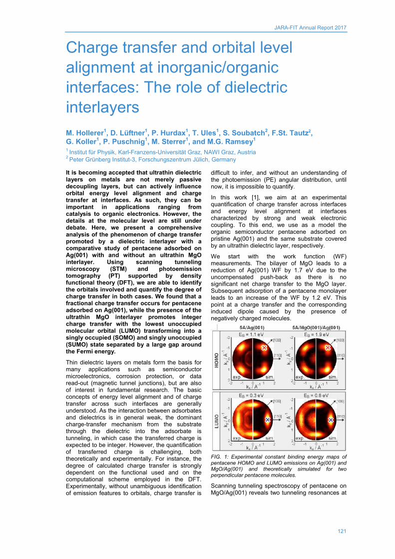
JARA-FIT Annual Report 2017
121
Charge transfer and orbital level alignment at inorganic/organic interfaces: The role of dielectric interlayers M. Hollerer1, D. Lüftner1, P. Hurdax1, T. Ules1, S. Soubatch2, F.St. Tautz2, G. Koller1, P. Puschnig1, M. Sterrer1, and M.G. Ramsey1 1 Institut für Physik, Karl-Franzens-Universität Graz, NAWI Graz, Austria 2 Peter Grünberg Institut-3, Forschungszentrum Jülich, Germany It is becoming accepted that ultrathin dielectric layers on metals are not merely passive decoupling layers, but can actively influence orbital energy level alignment and charge transfer at interfaces. As such, they can be important in applications ranging from catalysis to organic electronics. However, the details at the molecular level are still under debate. Here, we present a comprehensive analysis of the phenomenon of charge transfer promoted by a dielectric interlayer with a comparative study of pentacene adsorbed on Ag(001) with and without an ultrathin MgO interlayer. Using scanning tunneling microscopy (STM) and photoemission tomography (PT) supported by density functional theory (DFT), we are able to identify the orbitals involved and quantify the degree of charge transfer in both cases. We found that a fractional charge transfer occurs for pentacene adsorbed on Ag(001), while the presence of the ultrathin MgO interlayer promotes integer charge transfer with the lowest unoccupied molecular orbital (LUMO) transforming into a singly occupied (SOMO) and singly unoccupied (SUMO) state separated by a large gap around the Fermi energy.
Thin dielectric layers on metals form the basis for many applications such as semiconductor microelectronics, corrosion protection, or data read-out (magnetic tunnel junctions), but are also of interest in fundamental research. The basic concepts of energy level alignment and of charge transfer across such interfaces are generally understood. As the interaction between adsorbates and dielectrics is in general weak, the dominant charge-transfer mechanism from the substrate through the dielectric into the adsorbate is tunneling, in which case the transferred charge is expected to be integer. However, the quantification of transferred charge is challenging, both theoretically and experimentally. For instance, the degree of calculated charge transfer is strongly dependent on the functional used and on the computational scheme employed in the DFT. Experimentally, without unambiguous identification of emission features to orbitals, charge transfer is
difficult to infer, and without an understanding of the photoemission (PE) angular distribution, until now, it is impossible to quantify.
In this work [1], we aim at an experimental quantification of charge transfer across interfaces and energy level alignment at interfaces characterized by strong and weak electronic coupling. To this end, we use as a model the organic semiconductor pentacene adsorbed on pristine Ag(001) and the same substrate covered by an ultrathin dielectric layer, respectively.
We start with the work function (WF) measurements. The bilayer of MgO leads to a reduction of Ag(001) WF by 1.7 eV due to the uncompensated push-back as there is no significant net charge transfer to the MgO layer. Subsequent adsorption of a pentacene monolayer leads to an increase of the WF by 1.2 eV. This point at a charge transfer and the corresponding induced dipole caused by the presence of negatively charged molecules.
FIG. 1: Experimental constant binding energy maps of pentacene HOMO and LUMO emissions on Ag(001) and MgO/Ag(001) and theoretically simulated for two perpendicular pentacene molecules.
Scanning tunneling spectroscopy of pentacene on MgO/Ag(001) reveals two tunneling resonances at

JARA-FIT Annual Report 2017
122
-0.8 and +0.9 V. STM imaging at these voltages shows pentacene molecules oriented along [110] and [1-10] directions with a characteristic contrast resembling the shape of pentacene LUMO. We therefore conclude that molecules are singly occupied with SOMO state below and associated SUMO state above the Fermi energy (FE). The observed charge transfer is confirmed by theoretical calculations. To estimate the SOMO− SUMO gap, we calculated the electronic structure of an isolated molecule using an optimally tuned range-separated hybrid (OT-RSH) functional. The achieved gap (2.1 eV) is close to the one measured with STS (1.7 eV).
While the STM and DFT results are qualitatively in agreement, the unambiguous identification of the states may be problematic, owing to a possible influence of the tip, and the questions regarding the degree of charge transfer and the energy level alignment remain open. To this end, we employed the PT approach [2-4]. The simulations for the PE distribution from the HOMO and LUMO are shown in comparison to experimental constant binding energy (CBE) maps in Fig. 1. The agreement between these maps clearly identifies the corresponding emissions as HOMO and LUMO states and, hence, confirms the charge transfer for pentacene adsorbed on both Ag(001) and MgO/Ag(001). Note that on MgO/Ag(001) the pentacene LUMO is found 0.5 eV further below the FE than on bare Ag(001). Thus MgO film actually promotes charge transfer from the metal into the molecular layer. Moreover, the peak area of the LUMO emission has increased substantially due to the introduction of the MgO dielectric layer (Fig. 2).
FIG. 2: Photoemission spectra of pentacene on Ag(001) (a) and MgO/Ag(001) (b) measured at k positions of the HOMO (red) and LUMO (blue) intensity maxima in the momentum maps (marked with red/blue crosses in Fig.1). Normal emission spectra are shown with black. The peak areas of the HOMO and LUMO emissions are marked with red and blue shadings.
At the emission geometries of Fig. 2, the plane wave final-state simulations predict a HOMO/LUMO intensity ratio of 1.26 given the
orbitals have the same occupation. Assuming the HOMO occupancy to be 2 electrons, the relative experimental peak areas of the emissions can be used to estimate the LUMO filling. Analysis yields approx. 0.7 and 1.0 electrons per molecule for pentacene on Ag(001) and on MgO/Ag(001), correspondingly. This indicates the integer charge transfer to the pentacene LUMO and confirms the observation of a SOMO and SUMO states for all pentacene molecules on MgO/Ag(001) with STM.
With the entire set of experimental results, we can now draw a picture of the energy level alignment. For the bare Ag(001) surface, the measured WF sets the vacuum level (VL) to 4.3 eV above the FE. The adsorption of the MgO thin film reduces VL to 2.6 eV due to a 1.7 eV reduction of the WF caused by the push-back effect. This brings the pentacene LUMO very close to the FE, enabling charge transfer from the substrate into the molecule. While the LUMO stays pinned at the FE, the interface dipole created by the charged molecules leads to an increase of the WF by 1.2 eV and a corresponding shift of the HOMO level by the same magnitude. Because charge transfer through the dielectric barrier occurs by tunneling, the LUMO is occupied by an integer amount of charge, and the resulting singly occupied LUMO is split into a SOMO and a SUMO state separated by a gap of 1.7 eV, as determined by STS.
In conclusion, our study of the adsorption of pentacene on Ag(001) and Ag(001)-supported MgO thin films provides a clear and comprehensive understanding of charge transfer and energy level alignment at these model inorganic/ organic interfaces at a molecular level. The use of MgO(001) as thin dielectric layer enables us to demonstrate the transition from fractional charge transfer at the metal−organic interface to integer charge occupation of the molecular LUMO on an electronically decoupling, low-WF substrate. Our study unambiguously identifies the SOMO and SUMO of the singly charged pentacene anion adsorbed on the thin dielectric MgO layer and introduces an approach that permits the quantitative determination of the frontier orbital occupation.
[1] M. Hollerer, D. Lüftner, P. Hurdax, T. Ules, S. Soubatch, F. S. Tautz, G. Koller, P. Puschnig, M. Sterrer, and M. G. Ramsey, ACS Nano 11, 6252 (2017)
[2] P. Puschnig, S. Berkebile, A. J. Fleming, G. Koller, K. Emtsev, T. Seyller, J. D. Riley, C. Ambrosch-Draxl, F. P. Netzer, and M. G. Ramsey, Science 326, 702 (2009)
[3] P. Puschnig, E.-M. Reinisch, T. Ules, G. Koller, S. Soubatch, M. Ostler, L. Romaner, F. S. Tautz, C. Ambrosch-Draxl, and M. G. Ramsey, Phys. Rev. B 84, 235427 (2010)
[4] P. Puschnig, A. D. Boese, M. Willenbockel, M. Meyer, D. Lüftner, E. M. Reinisch, T. Ules, G. Koller, S. Soubatch, M. G. Ramsey, and F. S. Tautz, J. Phys. Chem. Letters 8, 208 (2017)
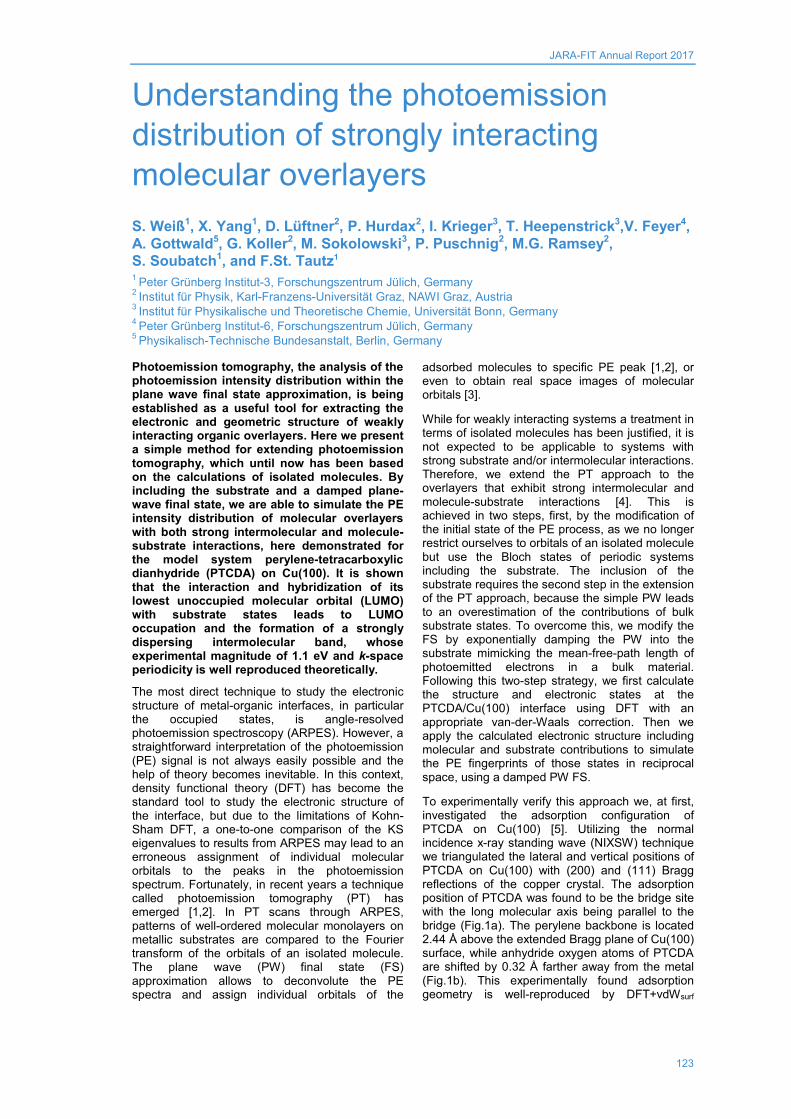
JARA-FIT Annual Report 2017
123
Understanding the photoemission distribution of strongly interacting molecular overlayers S. Weiß1, X. Yang1, D. Lüftner2, P. Hurdax2, I. Krieger3, T. Heepenstrick3,V. Feyer4, A. Gottwald5, G. Koller2, M. Sokolowski3, P. Puschnig2, M.G. Ramsey2, S. Soubatch1, and F.St. Tautz1 1 Peter Grünberg Institut-3, Forschungszentrum Jülich, Germany 2 Institut für Physik, Karl-Franzens-Universität Graz, NAWI Graz, Austria 3 Institut für Physikalische und Theoretische Chemie, Universität Bonn, Germany 4 Peter Grünberg Institut-6, Forschungszentrum Jülich, Germany 5 Physikalisch-Technische Bundesanstalt, Berlin, Germany Photoemission tomography, the analysis of the photoemission intensity distribution within the plane wave final state approximation, is being established as a useful tool for extracting the electronic and geometric structure of weakly interacting organic overlayers. Here we present a simple method for extending photoemission tomography, which until now has been based on the calculations of isolated molecules. By including the substrate and a damped plane-wave final state, we are able to simulate the PE intensity distribution of molecular overlayers with both strong intermolecular and molecule-substrate interactions, here demonstrated for the model system perylene-tetracarboxylic dianhydride (PTCDA) on Cu(100). It is shown that the interaction and hybridization of its lowest unoccupied molecular orbital (LUMO) with substrate states leads to LUMO occupation and the formation of a strongly dispersing intermolecular band, whose experimental magnitude of 1.1 eV and k-space periodicity is well reproduced theoretically.
The most direct technique to study the electronic structure of metal-organic interfaces, in particular the occupied states, is angle-resolved photoemission spectroscopy (ARPES). However, a straightforward interpretation of the photoemission (PE) signal is not always easily possible and the help of theory becomes inevitable. In this context, density functional theory (DFT) has become the standard tool to study the electronic structure of the interface, but due to the limitations of Kohn-Sham DFT, a one-to-one comparison of the KS eigenvalues to results from ARPES may lead to an erroneous assignment of individual molecular orbitals to the peaks in the photoemission spectrum. Fortunately, in recent years a technique called photoemission tomography (PT) has emerged [1,2]. In PT scans through ARPES, patterns of well-ordered molecular monolayers on metallic substrates are compared to the Fourier transform of the orbitals of an isolated molecule. The plane wave (PW) final state (FS) approximation allows to deconvolute the PE spectra and assign individual orbitals of the
adsorbed molecules to specific PE peak [1,2], or even to obtain real space images of molecular orbitals [3].
While for weakly interacting systems a treatment in terms of isolated molecules has been justified, it is not expected to be applicable to systems with strong substrate and/or intermolecular interactions. Therefore, we extend the PT approach to the overlayers that exhibit strong intermolecular and molecule-substrate interactions [4]. This is achieved in two steps, first, by the modification of the initial state of the PE process, as we no longer restrict ourselves to orbitals of an isolated molecule but use the Bloch states of periodic systems including the substrate. The inclusion of the substrate requires the second step in the extension of the PT approach, because the simple PW leads to an overestimation of the contributions of bulk substrate states. To overcome this, we modify the FS by exponentially damping the PW into the substrate mimicking the mean-free-path length of photoemitted electrons in a bulk material. Following this two-step strategy, we first calculate the structure and electronic states at the PTCDA/Cu(100) interface using DFT with an appropriate van-der-Waals correction. Then we apply the calculated electronic structure including molecular and substrate contributions to simulate the PE fingerprints of those states in reciprocal space, using a damped PW FS.
To experimentally verify this approach we, at first, investigated the adsorption configuration of PTCDA on Cu(100) [5]. Utilizing the normal incidence x-ray standing wave (NIXSW) technique we triangulated the lateral and vertical positions of PTCDA on Cu(100) with (200) and (111) Bragg reflections of the copper crystal. The adsorption position of PTCDA was found to be the bridge site with the long molecular axis being parallel to the bridge (Fig.1a). The perylene backbone is located 2.44 Å above the extended Bragg plane of Cu(100) surface, while anhydride oxygen atoms of PTCDA are shifted by 0.32 Å farther away from the metal (Fig.1b). This experimentally found adsorption geometry is well-reproduced by DFT+vdWsurf

JARA-FIT Annual Report 2017
124
calculations [4] used to theoretically determine the electronic properties of PTCDA/Cu(100) interface.
FIG. 1: (a) The adsorption site of PTCDA on Cu(100) and (b) the vertical geometry of PTCDA (side view along the long molecular axis).
Further, we applied ARPES and, in particular, PT to investigate the valence states of PTCDA/Cu(100). We found that the hybridization of the PTCDA LUMO with metal states of copper leads to its occupation and the formation of a highly dispersing intermolecular band (Fig. 2a), whose experimental magnitude and character are well reproduced by the theoretical approach described above. Experimental and theoretical energy distribution maps and constant binding energy (CBE) maps (Fig. 2b) are in good agreement. The observed CBE intensity pattern can be understood as that of an isolated PTCDA molecule modified by intermolecular band dispersion that has been strongly enhanced by molecule-substrate interactions. These strong interactions, which lead to a hybridization of molecule and substrate states, correlate with the small adsorption height of the molecule, with the carbon backbone closest to the metal surface among all other PTCDA adsorption heights measured so far.
In conclusion, we presented a method to simulate the PE intensity distribution of molecular overlayers that exhibit strong intermolecular and molecule-substrate interactions. We show that the initial state of the photoemission process can be approximated by the Bloch states of the entire calculated overlayer-substrate system and the FS by a damped PW.
FIG. 2: (a) Energy distribution map of PTCDA/Cu(100) showing dispersing intermolecular band originated from PTCDA LUMO and (b) experimental (left part) and theoretical (right) constant binding energy maps at the binding energy corresponding to the dispersing LUMO band in (a).
Furthermore, we demonstrate that the method allows the characterization of the electronic structure of an organic/metallic interface beyond a simple assignment of PE peaks to particular molecular orbitals in the PE spectrum. Specifically, we are able to reproduce the observed strong intermolecular dispersion of the molecule’s LUMO, which is significantly enhanced through substrate interactions, in terms of both its momentum map pattern and its bandwidth. As such, our approach extends the PT technique to strongly interacting systems allowing their rather complex photoemission intensity distribution to be simply understood.
[1] P. Puschnig et al., Science 326, 702 (2009) [2] P. Puschnig et al., Phys. Rev. B 84, 235427 (2010). [3] S. Weiß et al., Nat. Comm. 6, 8287 (2015) [4] D. Lüftner et al., Phys. Rev. B. 96, 125402 (2017) [5] S. Weiß et al., Phys. Rev. B. 96, 075414 (2017)

JARA-FIT Annual Report 2017
125
Control of morphology and formation of highly geometrically confined magnetic skyrmions Ch. Jin1,2, Z.-A. Li3,4,5, A. Kovács3, J. Caron3, F. Zheng3, F. N. Rybakov6,7,8, N. S. Kiselev9, H. Du1,10, St. Blügel9, M. Tian1,10, Y. Zhang1,10, M. Farle4,11, and R. E. Dunin-Borkowski3 1 The Anhui Key Laboratory of Condensed Matter Physics at Extreme Conditions, Hefei, China. 2 Department of Physics, University of Science and Technology of China, Hefei, China. 3 Ernst Ruska-Centre for Microscopy and Spectroscopy with Electrons and Peter Grünberg Institute,
Forschungszentrum Jülich, Germany. 4 Faculty of Physics and Center for Nanointegration (CENIDE), University of Duisburg-Essen, Germany. 5 Institute of Physics, Chinese Academy of Sciences, Beijing, China. 6 M.N. Miheev Institute of Metal Physics, Ekaterinburg, Russia. 7 Ural Federal University, Ekaterinburg, Russia. 8 KTH Royal Institute of Technology, Stockholm, Sweden. 9 Peter Grünberg Institute and Institute for Advanced Simulation, Forschungszentrum Jülich, Germany. 10 Collaborative Innovation Center of Advanced Microstructures, Nanjing University, China. 11 Center of Functionalized Magnetic Materials, Immanuel Kant Baltic Federal University, Kaliningrad,
Russia. One of the prerequisites for incorporating magnetic skyrmions representing nanoscale particle-like magnetic objects into spintronic devices, is the ability to controllably manipulate them in nanostructured elements. The direct visualization of varying morphology as well as details of the skyrmion nucleation process in a wedge-shaped FeGe nanostripe of width in the range of 45–150 nm was obtained by means of state-of-the-art holographic electron microscopy technique. We have shown that geometrically-confined skyrmions in a nanostripe are able to adopt their shape. This effect is not observed even in thin films of bulk materials. Moreover, our observation revealed that the most efficient approach for skyrmion nucleation in nanostripes is the continuous transformation of a helical spiral with increasing external magnetic field. The experimental observations are confirmed by a theoretical analysis based on the most general three-dimensional model for isotropic chiral magnets.
Magnetic storage in hard disk drive technology is based on the controllable formation of magnetic domains and is approaching its limits. The ability to manipulate domain walls instead of domains provides an alternative way to further extend the storage device roadmap [1]. The discovery of topologically stable magnetic skyrmions is of great interest because of their small size (typically below 100 nm) and their high mobility at low-current densities [1,2]. In particular, skyrmions are promising candidates for applications in novel data storage devices based on the race-track memory concept [1]. The underlying design of such devices relies on the use of skyrmions as data bit carriers, which move along a ferromagnetic nanostripe that
takes on the role of a guiding track. It is therefore important to be able to controllably form and manipulate skyrmions in nanostructured elements.
Despite a large body of experimental work on magnetic skyrmions reported in recent years, the formation and manipulation of skyrmions has never been studied in detail in highly confined geometries if the size of the sample is comparable to the size of the of skyrmions. -
FIG.1: Schematic representation for the chains of skyrmion tubes in nanostripes of varying width Wy. For very narrow stripes skyrmions show longitudinal ellipticity in a. For the critical width of the stripe Wy
c circular skyrmions appear in b. Above Wy
c skyrmions show transverse ellipticity in c. Above the width of Wy
t – the second critical width skyrmions are arranged in the form of a zigzag chain, as shown in d. The isosurfaces correspond to mz=0. The colours represent the magnetization direction on the unit sphere, see inset. a and b are the semi-axes of the skyrmions along and perpendicular to the nanostripe, respectively. Adapted from Ref. [3].
The optimization of information storage requires an optimal width for a nanostrip that hosts a chain of skyrmions, as well as precise control of their morphology and formation in such a confined

JARA-FIT Annual Report 2017
126
geometry. Our study is directly connected to the determination of the smallest width of a nanostrip that is still able to host magnetic skyrmions over a wide range of applied fields and temperatures.
FIG. 2: Magnetic induction maps recorded by means of off-axis EH in FeGe nanostripes. a and e Bright-field TEM image of the wedge-shaped sample. The white frames show the regions from which magnetic induction maps were recorded. The induction maps in b–d show the magnetic field dependence of the spin texture at temperature of 220 K and in f–k for a temperature of 95 K. The direction of the measured in-plane magnetic induction follows the colour wheel shown in b. The short straight white arrows in c, d, g, h, j show the direction of the spins around the edge of the nanostripe. A zigzag skyrmion chain is marked by a white frame in d. A one-to-one correspondence in the helix-to-skyrmion transformation, where each helix corresponds to a skyrmion, is indicated by the dotted white lines in f–h and i, j. The k-vectors in b, f, i indicate the propagation wave vectors of the magnetic helix. The scale bars in b,f correspond to 150 nm. Adapted from Ref. [3].
In general, the stability of skyrmions in chiral magnets, such as MnSi, FexCo1-xSi, FeGe and other B20 alloys, is governed by the Dzyaloshinskii–Moriya interaction (DMI). Competition between the DMI and ferromagnetic exchange coupling results in a homochiral spin helix ground state with an equilibrium period LD, which is determined by the ratio of the energy contributions of these two terms. At the external applied field, the energetically favourable state corresponds to the skyrmion lattice, which has nearly the same lattice constant in both bulk compounds and thin films, while skyrmions or more precisely skyrmion tubes adopt approximately circular shapes. Both theoretical analyzes and experimental observations suggest that elliptical distortions of skyrmions in extended systems are associated with a loss of stability, which is referred to as an elliptical or strip-out instability. The
theoretical calculations for equilibrium skyrmion states based on a general model for a three-dimensional isotropic chiral magnet in nanostripes suggest a completely different behaviour of skyrmions, see Fig. 1. In particular, for a long nanostripe of width Wy on the order of the skyrmion size and length Wx>>Wy, the theory predicts a loss of radial symmetry of skyrmions without loss of their stability. Moreover, it is predicted that the skyrmion morphology of a single chain of skyrmions will depend on the nanostripe width Wy in a particular range of applied magnetic fields. The dimensions of the elliptical skyrmion shapes can be described in terms of their semi-axes a and b along and perpendicular to the nanostripe, respectively, see Fig. 1a. For nanostripe widths close to a critical value Wy
c, skyrmions exhibit circular shapes (a=b), while for Wy<Wy
c and Wy>Wy
c a longitudinal (a>b) or a transverse (a<b) ellipticity is predicted. Upon further enlargement of the nanostripe width above a second critical value Wy
t, the skyrmions are expected to be arranged in equilibrium in the form of a zigzag chain.
To test these predictions, we carefully fabricated a wedge-shaped nanostripe from a bulk crystal of FeGe using a lift-out method [3]. The nanostripe had a thickness L of 110 nm, a length Wx of ~2.6 mm and a width Wy that varied linearly from ~10 to ~180nm, see Fig. 2a, e. This range of widths is designed to include the helical period LD=70 nm of bulk FeGe. Figure 2b–d, f–k show quantitative magnetic induction maps of the spin texture measured experimentally in the presence of different external magnetic fields using off-axis EH, with the directions and magnitudes of the projected in-plane magnetization fields. We find a very good quantitative agreement between experimental observations and theoretical predictions; see the shape of elliptically distorted skyrmions in a narrow and wide part of the nanostripe in Fig. 2c, j, k. Our results can be considered for several potential applications. The high flexibility of spatially-confined magnetic skyrmions allows them to adapt their shape and size in a nanostructure. This allows us to predict unique oscillating and stretch-out excitation modes in alternating magnetic fields for elliptically-distorted skyrmions in nanostripes. Another important aspect revealed by our observations is the direct visualization of a mechanism of skyrmion nucleation, which is almost independent of their initial state and characterized by the conservation of skyrmion number with respect to the number of helical spirals in the nanostripe. Such a simple approach for nucleation of a predefined number of skyrmions by varying the applied magnetic field seem to be highly suitable for applications in spintronic devices.
[1] A. Fert et al. Nat. Nanotechnol. 8, 152 (2013) [2] N. Nagaosa et al. Nat. Nanotechnol. 8, 899 (2013) [3] C. Jin et al. Nat. Commun. 8, 15569 (2017)

JARA-FIT Annual Report 2017
127
Controlling the growth of multiple ordered heteromolecular phases by utilizing intermolecular repulsion C. Henneke, J. Felter, D. Schwarz, F. St. Tautz, and C. Kumpf Peter Grünberg Institut-3, Forschungszentrum Jülich, Germany Metal-organic interfaces and their structural, electronic, and thermodynamic properties have been investigated intensively, aiming to improve and develop future electronic devices. In this context, heteromolecular phases add new design opportunities simply by combining different molecules. However, controlling the desired phases in such complex systems is a challenging task. Here, we report an effective way of steering the growth of a bimolecular system composed of adsorbate species with opposite intermolecular interactions, repulsive and attractive, respectively. The repulsive species forms a two-dimensional lattice gas, the density of which controls which crystalline phases are stable. Critical gas phase densities determine the constant-area phase diagram that describes our experimental observations, including eutectic regions with three coexisting phases. We anticipate the general validity of this type of phase diagram for binary systems containing two-dimensional gas phases, and also show that the density of the gas phase allows engineering of the interface structure. The minimization of thermodynamic potentials is a well established concept for predicting structures and phases that are stable in thermodynamic equilibrium. For surfaces, the surface free energy is the relevant quantity that -- plotted versus chemical potentials -- allows the identification of
stable surface reconstructions. If, for the exemplary case of a binary crystal AxBy, the chemical potential shifts towards one side (e.g., towards A, by deposition of species A on the surface), one expects the system to respond by forming a more A-rich surface reconstruction. It would be very surprising if in such a case a more B-rich phase was observed. However, this is precisely what we find for the system under study, opening an intriguing way to control phase formation via critical densities in a gas phase. We have investigated heteromolecular submonolayer films formed by 3,4,9,10-perylenetetracarboxylic dianhydride (PTCDA) and copper-phthalocyanine (CuPc). Adsorbed on Ag(111), the molecules show different intermolecular interaction and therefore also different growth behaviors (compact islands and a two-dimensional (2D) lattice gas, respectively). Combined within one molecular layer, these molecules form three crystalline heteromolecular phases with different stoichiometries -- P2C, PC and PC2 (P=PTCDA, C=CuPc) -- which always coexist with 2D gas phase areas on the surface. As we demonstrate here, it is the density of this gas phase that determines which of the crystalline phases are stable, whereby -- most remarkably -- up to three phases (two crystalline and the gas phase) may coexist in large regions of the constant-area phase diagram.
FIG. 1: Deposition of CuPc on a 0.17ML film of PTCDA/Ag(111) at 380K. (a) Pathway in the phase diagram. (b-h) Bright-field LEEM images showing PTCDA islands (green), sequentially transforming into P2C (yellow), PC (red), and PC2 (blue) with increasing CuPc coverage. A movie is available with the original publication. (i) LEEM intensity of the gas phase areas during CuPc deposition.

JARA-FIT Annual Report 2017
128
Hence, large eutectic regions exist, in contrast to eutectic points as observed for, e.g., intermetallic phases. We present a generic model of wide applicability explaining this type of phase diagram. Fig. 1 shows a typical series of LEEM images recorded during CuPc deposition on a Ag(111) surface partially covered by PTCDA. The first LEEM image (panel b) shows bright PTCDA islands (green arrows) while the clean Ag(111) surface appears dark and becomes even darker during CuPc deposition due to the formation of the 2D lattice gas (white arrows in c-h). When a certain amount of CuPc has been deposited, the PTCDA islands transform to the P2C phase (medium contrast, yellow arrows). When this first transformation is completed and CuPc is further deposited, the islands eventually transform into (much smaller) PC islands (red arrows), and finally into PC2 islands (blue arrows). We have performed 22 such deposition series with different deposition sequence and constructed the phase diagram shown in Fig. 2. While only one crystalline phase is present in some regions (unicolored data points), we also found four large eutectic regions with two coexisting crystalline phases (bicolored data points). The experiment displayed in Fig. 1 is marked by a blue dashed arrow labeled “CuPc deposition”. It runs horizontally through all regions from the most PTCDA-rich to the most CuPc-rich phase. Experiments performed with inverted deposition sequence are described in the original work.
FIG. 2: Phase diagram for the heteromolecular PTCDA+CuPc adsorbate system. The color code of the data points indicates crystalline structure(s) found in the experiment at the corresponding partial coverages Colored areas mark the regimes of pure and eutectic regions as obtained from the model. A 2D lattice gas phase also exists all over the phase diagram. Red and blue circles and the blue dashed line are explained in the text. For all other details, see original publication.
Additionally to one or two crystalline phases, the gas phase also exists at all coverages below 1ML due to the repulsive intermolecular interaction of CuPc. The gas acts as a reservoir of CuPc molecules. Its density represents the critical
parameter, which determines the structure of the entire phase diagram: For the experiment shown in Fig. 1b-h, the LEEM intensity of gas phase regions is plotted versus the CuPc coverage in Fig. 1i. The intensity changes during deposition, except in the grayish areas where it remains constant. Here, also the gas phase density is constant, since it correlates directly with the LEEM intensity. These sections precisely correspond to eutectic regions in the phase diagram. Hence, the density of the gas phase rises only when only one crystalline phase is present on the surface, during the phase transformations it remains constant. This behavior is explained as follows: Initially, CuPc molecules being deposited increase the gas phase density, PTCDA islands remain unaffected. When a certain critical density is reached (first marker in Fig. 1i), the transformation PTCDA → P2C starts. Now, all additional CuPc molecules are incorporated in P2C islands, the density of the gas phase remains constant (see Fig. 1b and c). This process continues until all PTCDA islands have been transformed (second marker in Fig. 1i). Only afterwards the additional CuPc enters the gas phase again increasing its density further. This scenario repeats when the next critical density is reached. Hence, the existence of a critical CuPc gas phase density for each of the eutectic regimes explains the observation. Phase transformations are triggered by reaching these critical densities.
In the original publication we derive a generic model for the phase diagrams of such hetero-molecular systems based on two fundamental assumptions: (i) The molecular species form at least one crystalline heteromolecular phase, and (ii) one of the species exhibits intermolecular repulsion and yields a 2D lattice gas. Without any reference to specific material properties, the model explains and quantifies the zig-zag pattern of straight lines separating the different regions in the phase diagram. These boundaries are fixed by the five single-phase points on the 1ML-line (red circles in Fig. 2, fixed by the stoichiometry of the phases), and by four points on the abscissa (blue circles, critical gas phase densities).
We conclude that the submonolayer phase diagram can be fully understood by the existence of critical gas phase densities, which in turn follows from generic thermodynamic considerations based on the Helmholtz free energy of the phases involved. The gas phase density is the decisive quantity, since it determines which phase(s) is/are stable on the surface. Once the critical values are known, they can be utilized to gain control over the layer growth and to design the surface in terms of the desired homo- and heteromolecular crystalline phases. The key property, which enables this remarkable freedom in engineering metal-heteroorganic contacts, is the intermolecular repulsion of the CuPc molecules in the 2D lattice gas.
[1] C. Henneke, J. Felter, D. Schwarz, F. S. Tautz, and C. Kumpf, Nature Materials 16, 628 (2017)

JARA-FIT Annual Report 2017
129
Epitaxy of Si-Ge-Sn-based hetero-structure light emitters N. von den Driesch1,2, D. Stange1, D. Rainko1, I. Povstugar3, G. Capellini4, Z. Ikonić5, J.M. Hartmann6, S. Mantl1, D. Grützmacher1,2, and D. Buca1 1 Peter Grünberg Institute-9, Forschungszentrum Jülich, Germany 2 JARA-Institute Green IT (PGI 10), RWTH Aachen, Germany 3 Central Institute for Engineering, Electronics and Analytics (ZEA 3), Forschungszentrum Jülich, Germany 4 IHP Microelectronics, Germany and Università Roma Tre, Italy. 5 Institute of Microwaves and Photonics, University of Leeds, United Kingdom 6 Univ. Grenoble Alpes, CEA, LETI, Grenoble, France The recent development of group IV-based direct bandgap semiconductors and their demonstration as lasers have strengthened the efforts to fabricate monolithically integratable light emitters. Such Si-congruent solution enables merging of state-of-the-art electronics with photonic devices on the same chip improving energy efficiency and versatility of those. To further advance this field, the epitaxy of different GeSn/SiGeSn heterostructures was explored, aiming for emitters with higher emission efficiency. Atom distribution and crystalline quality of the complex double- (DHS) and multi quantum well (MQW) heterostructures were investigated. The optical quality indicates a strong enhancement for MQW, since deleterious dislocations can be avoided. Furthermore, the effect of energy quantization in MQW structures is proven.
Group IV-based materials, in particular silicon (Si), fuel our smartphones and build the foundation of our modern digital society. The ever-increasing demand for data bandwidth and energy efficiency requires new solutions, such as purely optical on-chip communication. The mandatory requirement, however, a direct bandgap material, is not available within group IV elements. Alloying of germanium (Ge) with tin (Sn) has shown to deliver such and enabled optically pumped lasing, yet only at cryogenic temperatures [1], [2]. To further improve the emission characteristics of the material, different configurations of GeSn/SiGeSn heterostructures, namely DHS and MQW, were grown. In such structures, carriers are confined in the optically active region far away from defective interfaces, which enhances the recombination efficiency.
The material stacks were deposited in an industry-compatible reduced-pressure chemical vapor deposition (RP-CVD) reactor on 200 mm Si(001) wafers. The commercially available precursors digermane (Ge2H6), disilane (Si2H6) and tin tetrachloride (SnCl4) were employed which allow rather small growth temperatures below 375°C [3]–[5]. The first type of heterostructures are DHS, schematically shown in Fig. 1a. Initially, a roughly 200 nm thick GeSn buffer layer was grown to accommodate the large lattice mismatch between
GeSn and the underlying Ge-buffered Si wafer (Ge-VS). On top of this, a SiGeSn/GeSn/SiGeSn double heterostructure (DHS) was grown. Incorporation of Si atoms within the SiGeSn claddings elevate conduction and valence bands in those, ensuring a type I band alignment inside the layer stack.
FIG. 1: a) Schematics of the heterostructure material stack. b) Cross-sectional TEM micrograph and overlaid EDX profile of the grown DHS. c) Atom probe tomography (APT) data and corresponding elemental distributions.
SiGeSn claddings and GeSn active regions can be distinguished from the EDX elemental profiles, depicted in Fig. 1b. The high Sn incorporation of 14.5 at.% inside GeSn guarantees a direct bandgap in the active device region. Si atoms are only found within the ~50 nm thick SiGeSn carriers, as apparent from the Si profile in Fig. 1b (red line). The rather thick GeSn active region (~380 nm), however, provokes further plastic strain relaxation. Consequently, misfit dislocations are generated at the GeSn/SiGeSn interface, which deteriorate light emission efficiency. Such defects can be avoided in a different growth scheme, namely multi quantum wells (MQW). In this configuration, ten periods of GeSn/SiGeSn wells/barriers are grown, each with thicknesses of 22 nm. Even in such complex arrangement, Si atoms are present almost exclusively inside the SiGeSn barriers, as demonstrated by elemental concentration profiles from APT in Fig. 1c. The

JARA-FIT Annual Report 2017
130
main advantage of MQW structures over DHS is originated in the smaller volume of active material. Less compressive strain accumulates inside the structure, suppressing the formation of additional defects. Accordingly, the benefits should be visible in light emission, which is discussed in the following.
FIG. 2: a) Comparison of photoluminescence spectra at 4 K. b) Temperature-dependent PL for different structures.
Photoluminescence spectra of bulk GeSn, a DHS and a MQW structure are shown at 4 K in Fig. 2a. The DHS shows only marginally increased emission compared to the bulk sample. The carrier confining effect from the SiGeSn barriers is masked by the material degradation from the presence of defects at the interface of the active region. In contrast, the MQW structure shows an order of magnitude enhanced light emission. This results from both the confinement of carriers inside the GeSn wells and their geometrical separation from the defective GeSn buffer layer. The observed enhancement can be analyzed more closely from its temperature dependence, shown in Fig. 2b. The distinct advantage of the MQW structure vanishes at temperatures above 150 K. This is related to the still rather small conduction band offset between GeSn wells and SiGeSn barriers (13 meV from band-structure calculations). At elevated temperatures, carriers are able to escape from the well regions, rendering the energetic barriers inoperative. To account for that degradation, optimized future heterostructures need to further increase the amount of incorporated Si inside the barriers.
FIG. 3: Comparison of PL emission and conduction band alignment in MQW samples with different well thicknesses.
Finally, the effect of energy quantization inside the multi quantum well structures is investigated. To that end, a second MQW structure was epitaxially grown, differing from the previous one only in the GeSn well thickness of 12 nm. PL spectra and conduction band positions are juxtaposed in Fig. 3 at 4 K. In case of the sample with thinner (12 nm vs. 22 nm) wells, PL emission is shifted towards larger energies. The quantum confinement in z-direction leads to a band energy splitting into quantized levels, depending on layer thickness. Thus, the observed distinct blueshift of 20 meV can be attributed to the stronger quantization effect inside the thinner wells. Accordingly, the observed light emission stems from quantized states, implying additional benefits for future lasers, made from GeSn/SiGeSn quantum well heterostructures. To sum up, we demonstrated the epitaxy of group IV-based heterostructures, comprising of direct bandgap GeSn active regions and SiGeSn barriers. Both double heterostructures and multi quantum wells demonstrate a high structural and crystalline quality. MQWs benefit from the lack of additional misfit defects, which was shown to strongly improve light emission characteristics, at least at cryogenic temperatures. Emission from quantized levels in the MQW proves a reduced 2D density of states, which makes MQW heterostructures promising candidates for efficient group IV-based emitters.
This research received financial support from the BMBF in frame of the M-ERA.NET project GESNAPHOTO and from the DFG for project “SiGeSn Laser for Silicon Photonics”.
[1] S. Wirths, R. Geiger, N. von den Driesch, G. Mussler, T. Stoica, S. Mantl, Z. Ikonić, M. Luysberg, S. Chiussi, J.-M. Hartmann, H. Sigg, J. Faist, D. Buca, and D. Grützmacher, Nat. Photonics 9 (2), 88 (2015)
[2] J. Margetis, S. Al-Kabi, W. Du, W. Dou, Y. Zhou, T. Pham, P. Grant, S. Ghetmiri, A. Mosleh, B. Li, J. Liu, G. Sun, R. Soref, J. Tolle, M. Mortazavi, and S.-Q. Yu, ACS Photonics 5 (3), 827 ( 2018)
[3] N. von den Driesch, D. Stange, S. Wirths, G. Mussler, B. Holländer, Z. Ikonić, J.-M. Hartmann, T. Stoica, S. Mantl, D. Grützmacher, and D. Buca, Chem. Mater. 27 (13), 4693 (2015)
[4] N. von den Driesch, D. Stange, S. Wirths, D. Rainko, I. Povstugar, A. Savenko, U. Breuer, R. Geiger, H. Sigg, Z. Ikonić, J.-M. Hartmann, D. Grützmacher, S. Mantl, and D. Buca, Small 13, 1603321 ( 2017)
[5] N. von den Driesch, D. Stange, D. Rainko, I. Povstugar, P. Zaumseil, G. Capellini, T. Schröder, T. Denneulin, Z. Ikonić, J.-M. Hartmann, H. Sigg, S. Mantl, D. Grützmacher, and D. Buca, Adv. Sci. 5, 1700955 ( 2018)

JARA-FIT Annual Report 2017
131
Graphene bioelectronics D. Kireev, P. Shokoohimehr, M. Brambach, V. Maybeck, B. Wolfrum, and A. Offenhäusser Institute of Complex Systems-8, Bioelectronics, Forschungszentrum Jülich, Germany Human brain is possibly the most complex organism. Understanding the human brain is one of the most important aims of bioelectronics as a research field. Electrogenic cells, such as neurons, that define human brain are organized in a highly complex, three-dimensional structure. Moreover, placing an inorganic object inside the brain tissue would cause an ultimate rejection and failure of the implant. Therefore, tools that are used for interfacing with brain must be infinitely thin, yet robust, conductive and biocompatible. As we show, graphene is the ultimate material for this purpose. Tested for in vitro electrophysiology, it shows excellent ability to measure cellular activity, as well as novel in vivo designed graphene-based probes are under investigation.
Graphene transistors - The graphene-based, solution-gated field effect transistor arrays (GFETs) are fabricated on a large scale for bioelectronic measurements (see fig. 1). As we studied variety of gate geometries (width/length) of the graphene channel, we reveal a linear relation between the transconductance and the width/length ratio. Nonetheless, the typical area-normalized electrolyte-gated transconductance is in the range of 1-2 mS·V-1·and does not strongly depend on the substrate.
FIG. 1: Schematics of a liquid-gated GFET.
The devices are used as a proof-of-concept for bioelectronic sensors, recording external potentials from both: ex vivo heart tissue and in vitro cardiomyocyte-like HL-1 cells. A typical time trace recording from a GFET with HL-1 action potentials is shown in Fig. 2. The cells are beating (producing repetitive action potentials (APs) that propagate through the whole cellular layer) with a rate over 25 bpm and an amplitude of 1.2±0.2 mV. The overall SNR of the recordings is 6±1, which is in the same sensitivity range as reported previously. The shape of the APs is also shown in Fig. 2, where over 115 consecutive spikes are averaged and the average AP is shown in blue. The shape of the action potential, in agreement with previous works, indicates a very good sealing between the cell and the transistor [1]. Further, cortical neurons were cultured on top of the chips with an approximate density of 1500 cells per mm2.
FIG. 2: HL-1 and neuronal APs recorded with GFETs.
The neuronal networks were cultured 14 days in vitro (DIV14) until mature, when the cultured neurons produce spontaneous APs that can propagate through the network. As expected, the extracellular neuronal APs are one or two orders of magnitude smaller than those of heart tissue45. Nevertheless, we are able to record the APs and even bursting activity of neuronal networks with the GFETs (Fig. 2). The in vitro neuronal signals as recorded by the graphene transistors with distinguishable bursting-spiking pattern for the first time [1].
Graphene microelectrodes - Multielectrode array design is probably the simplest for bioelectronics devices that exist there. Graphene-based electrodes, arranged into an array, result in a GMEA chip (see fig. 3), which is similar to the classical MEAs. Such simple potentiometric devices display remarkable features in cell electrophysiology. Assuming ideal passivation and infinite input impedance, the GMEAs can directly pick-up these changes in cell membrane potential, since they operate as voltage-followers. Furthermore, currently state-of-the-art technology desires to combine electrophysiology with other methods, such as calcium imaging and optogenetics, and that the requirement of transparency for such electrodes is of greatest importance.
FIG. 3:. Schematics of a liquid-operated GMEA.
Graphene multielectrode arrays, presented in this work, feature 64 active sites with 10 and 20 um diameter passivation openings (see Fig. 4a-b). The multichannel measurement set-up allows us to measure the whole chip in parallel. An example of the simultaneously recorded timetraces from HL-1 cells is given in Fig. 4d. The clearly visible delay

JARA-FIT Annual Report 2017
132
between APs on different channels shows that the signal propagates through the cellular layer. The propagation velocity and map can be deduced from the timestamps of the action potentials and corresponding geometry of the channels. The recorded action potential amplitudes and their shapes vary from chip to chip (culture effect) and from electrode to electrode (sealing effect). Over 13000 HL-1 action potentials from 104 recorded timeseries (complete chip arrays) were analyzed in order to compare them with the experimental and simulated data. Typical signal-to-noise ratio of HL-1 recordings is above 100 [2].
FIG. 4: (a-b) design of the GMEA chips. (c) SiO2/Si and glass-based GMEAs. (d) live dead image of the HL-1 cells (left) and typical timetrace recordings with GMEAs. (e) neuronal culture image (left) and typical timetrace patterns recorded with GMEAs.
Further, the same devices were for extensive in vitro study of cortical neuronal networks, and we found that they show excellent ability to extracellularly detect action potentials with signal to noise ratios up to 100 for spontaneous bursting/spiking neuronal activity (see Fig. 4e). Complex neuronal bursting activity patterns as well as a variety characteristic shape of HL-1 APs are also recorded with the GMEAs [2]. Clearly, the potential applications of the GMEAs in biological and medical research are still numerous and diverse.
Implantable graphene probes - As shown above, graphene-based devices are extremely sensitive and very useful in a wide spectrum of bioelectronics research. Here we describe a method to fabricate arrays of graphene-based probes, requiring minimal number of fabrication steps, while maintaining overall device functionality
as well as flexibility (see Fig. 5 and 6). The polyimide-based probes are approximately 6 µm thick, therefore ultra-flexible, yet robust and stable. Both, GFETs and GMEAs are fabricated in one run on one wafer [3].
FIG. 5: From rigid to flexible graphene-based devices.
The V-shaped transfer curves, that are typical for graphene, are recorded on the flexible GFETs. The devices seem to be stable and show characteristic performance similar to the state-of-the-art Si-based and polyimide-based GFETs [15].
FIG. 6: Optical images of freely standing graphene-based probes (a-c) and as bonded to a special carrier for in vivo use (d).
The maximum transconductance measured so far was in the range of 700 µS/V, which is comparable to typical polyimide-based GFETs. Impedance measurements of the graphene-based electrodes result in a typical interface capacitance of 20-60 pF (depending on the electrode diameter opening) and impedance values of 2-6 MΩ at 1 kHz [3]. The impedance values are rather high, yet in the range of the untreated graphene as reported previously [2].
[1] D. Kireev, M. Brambach, S. Seyock, V. Maybeck, W. Fu, B. Wolfrum, and A. Offenhäusser, Sci. Rep. 7, 6658 (2017)
[2] D. Kireev, S. Seyock, J. Lewen, V. Maybeck, B. Wolfrum, and A. Offenhäusser, Adv. Healthc. Mater. 6, 1601433 (2017)
[3] D. Kireev, P. Shokoohimehr, M. Ernst, V.R. Montes, K. Srikantharajah, V. Maybeck, B. Wolfrum, and A. Offenhäusser, MRS Adv. 3, 1621 (2018), 3,–7.

JARA-FIT Annual Report 2017
133
Neuronal Polarity by Controlling Axon Elongation or Dendritic Branching F. Milos, L. Du, A. Belu, L. Jin, D. Mayer, V. Maybeck, and A. Offenhäusser Institute of Complex Systems-8, Forschungszentrum Jülich, Germany Control of neural polarity is of great importance in order to promote directed nerve regeneration, build models for neural development, and allow neural-based in vitro computing operations. Neural polarity can be directed by both soluble factors or by surface cues. While most work focuses on defining the axon, we show that in addition to topographical structures promoting axon initiation, bifurcation of the neurite outgrowth path on patterned adhesion molecules is able to define dendritic branches. We show that within a framework of adhesive guidance molecules, it is the level of neurite branching that determines polarity by slowing growth, whereas topography can be used to accelerate neurite growth and axon determination. Live imaging studies suggest that in both manipulations it is a relative faster advancement of the axon compared to other neurites that determines polarity.
In the last few years, there have been many attempts to control the outgrowth of neurites so that neural cells can be wired together with defined axonal-dendritic connections. Methods applied include micro-contact printing of cell adhesive proteins, application of chemical gradients, and physical restriction of growth by microchannels or substrate topography. Most efforts have focused on forcing the formation of the axon in a particular direction. This is typically achieved by providing one path for fast outgrowth, promoting the neuron on this path to become the axon.
First, we used polymer substrates with defined nano-topography of different heights and diameters to alter neurite outgrowth. It was unclear what height difference was necessary for a neuron to recognize that a topography exists. OrmoComp polymer was nanostructured by nanoimprint lithography to generate culture substrates with a grid array of round projections. E18 rat cortical neurons were then cultured in vitro on these substrates and the development of the neurites was monitored.
We show that compared to growth on homogeneously flat substrates, axon determination occurred earlier in neurons grown on nano-topographies (see Fig. 1) [1]. The effect was stronger on taller structures with larger separation. The grid-like pattern of polymer projections induced the neuron to build preferentially straight neurites that followed either the rows or columns of the grid, or, to a lesser extent, the diagonal connecting topographical features. The initiation
and final angle also aligned to the layout of the topography on 400nm high structures. Since neurites spent less time exploring, a neurite could reach symmetry breaking length and become the axon earlier. The speed difference on topographical features compared to flat substrates is due to a combination of significantly more time spent elongating and a reduction in the amount of time spent pausing. Retraction of the neurite was not affected.
FIG. 1: Top: Frames taken from a live-imaging movie of a neuron growing on an OrmoComp nanotopography of bumps in vertical and horizontal rows. After 2 days of growth, the axon begins to express a fluorescent marker for actin. Bottom: Rate of axon initiation by 36 hours in vitro on flat vs. low (L) and high (H) topographical structures.
In contrast, when one neurite is given a straight path to follow and competing neurites are given branched paths, those neurites on the branched paths spend more time exploring and make slower progress. This slowed progress leads to biochemical and functional tendency to form dendrites. The branched structures to guide single neuron morphology used by Du et al. [2] are a rare example of defining the dendrites of a neuron in order to have directional axon projection instead of

JARA-FIT Annual Report 2017
134
targeting the behavior of the axon itself. These patterns were made of the cell adhesion promoting peptide PLL, and were patterned onto glass using micro-contact printing. In both immunocytological investigation and electrophysiology, the axon-dendrite direction was shown to be in the intended direction 53-69% of the time, depending on the angle and degree of branching. Stronger guiding effects were observed in patterns where the neurite had the most choices to explore at a given node of the pattern. The directionality in the event of random chance would have been only 30% for these patterns.
FIG. 2: Branched structures slow neurite outgrowth (top) so that functional directionality is achieved in chains of patterned neurons as determined by optogenetic stimulation. The right to left signal conduction triggers an action potential in cell 2 when cell 3 is stimulated by light, but not when cell 1 is stimulated as shown schematically in the middle and by patch clamp recording on the bottom.
The functional directionality of these patterns was tested optogenetically. Neurons expressing the blue-light-sensitive Channelrhodopsin ChR2opt were grown on patterned cells arranged in series. Patch clamp electrophysiology was used to measure the activity of a cell in the middle of the series while light stimulation drove action potentials in the cell itself or in the cell to either side on the pattern (Fig. 2). Electrophysiology recordings are consistent with immunostainings, showing a preferential connection between neurons with dendrites on the branched structures and the axon projecting in the opposite direction.
Our results show that the relative speed of neurite outgrowth is a critical factor in determining the directionality of neuronal signaling on defined patterns. Multiple methods, including restricted chemical adhesion points and topographical cues may be used to manipulate the speed of neurite outgrowth. These interventions can be used to define axonal position if they increase neurite outgrowth speed and to define dendritic trees if
they retard neurite outgrowth speed. A major factor contributing to neurite outgrowth appears to be the time a growth cone must spend investigating its surroundings. More choices of direction lead to slower progress of neurite outgrowth. This is supported by our measurements that the speed of neurite outgrowth on 400nm high patterned topologies is about 30% faster than that on flat OrmoComp substrates. However, when growth on a flat substrate is restricted to one dimension by adhesive proteins neurite outgrowth is even faster. Neurites restricted to one dimension by micro-contact printing except for the specific branch points of the pattern extended three times as fast as neurites growing in 2-dimensions on topographical patterns (9 µm/h vs. 3 µm/h). Neurites fully confined to 1-dimension with no branch points were again faster, reaching an extension speed of 15 µm/h. This further shows that it is consistently the relative neurite outgrowth speed that determines the axon/dendrite polarity of the neuron rather than the absolute outgrowth speed achieved.
In conclusion, we have developed multiple systems to modify the speed of neurite outgrowth in vitro and shown that the relative speed of neurite outgrowth can be used to determine neuronal polarity. This polarity includes morphological, biochemical, and functional directionality of the neuron. As such, these techniques provide a means to develop neural model systems with defined connectivity for the study of neural regeneration and bio-inspired information processing.
[1] F. Milos, A. Belu, D. Mayer, V. Maybeck, and A. Offenhäusser, submitted
[2] L. Du, L. Jin, G. Zhu, V. Maybeck, and A. Offenhäusser, in preparation

JARA-FIT Annual Report 2017
135
Coulomb-Engineering of Two-Dimensional Semiconductors for New Non-Classic Light Sources S. Borghardt1, J.-S. Tu1,2, D. Grützmacher1, and B. E. Kardynal1 1 Peter Grünberg Institut-9, Forschungszentrum Jülich, Germany 2 Helmholtz Nano Facility, Forschungszentrum Jülich, Germany In the recent years, strain-induced quantum emitters in atomically thin two-dimensional semiconductors such as transition-metal dichalcogenide monolayers (TMDC-MLs) have received a lot of attention [1,2]. Their optical properties render these single-photon sources promising candidates for new non-classic light sources. However, manipulating the materials’ band gap via strain with a high spatial and energetic precision remains a challenging task, precluding strain-induced quantum emitters from real-world applications. An auspicious alternative, which is unique to two-dimensional materials, relies on the local modulation of screening of the Coulomb interaction within the TMDC-ML through a local variation of the relative permittivity of the ML’s direct environment, also called Coulomb-engineering. In our work [3] we investigated different types of dielectrics as potential components for Coulomb-engineered lateral heterostructures in TMDC-MLs.
The ultimate thinness of two-dimensional semiconductors renders the interaction between charge carriers within these materials sensitive to the dielectric environment of the material. Figure 1 depicts how externally induced screening changes both the electronic band gap, 𝐸𝑔 , and the binding energy of the neutral exciton, 𝐸𝑏,𝑥 , in a TMDC-ML. The binding energy of the neutral exciton is given by the difference between 𝐸𝑔 and the ground state energy of the neutral exciton, 𝐸𝑥,1:
𝐸𝑏,𝑥 = 𝐸𝑔 − 𝐸𝑥,1
Binding energies of neutral excitons in TMDC-MLs are as high as several hundreds of meV. Both the electronic band gap and the binding energy of the neutral exciton are expected to decrease with an increasing relative permittivity of the surrounding dielectric. The sign of the change of the optical band gap, which is equivalent to 𝐸𝑥,1, depends on the relative change of 𝐸𝑔 and 𝐸𝑏,𝑥.
In our work, we employed low-temperature μ-photoluminescence, as well as reflectance measurements, to study MoSe2 and WSe2 MLs in different dielectric environments. Our results show a redshift of the optical band gaps, as well as a reduction of the binding energies of the neutral exciton, with an increasing relative permittivity of the ML’s surrounding.
FIG. 1: Schematic diagram of the effect of environment-induced dielectric screening on the electronic band gap, Eg, and on the excitonic states, Ex,n, in TMDC-MLs. Solid and waved arrows represent optical absorption and radiative recombination processes, respectively.
Estimates on the resulting changes of the electronic band gaps are made from the measured optical band gaps and exciton binding energies.
Figure 2 shows photoluminescence spectra for three representative structures.
FIG. 2: Representative photoluminescence spectra for WSe2 (a) and MoSe2 (b) MLs in different dielectric environments. The labels below (above) the horizontal line show the substrate (cover) material. The dotted line follows visually the evolution of the neutral excitons. The strongest line, which follows the same trend, is a charged exciton line. For WSe2, a band of defects can be observed at the low energy end of the spectra.

JARA-FIT Annual Report 2017
136
The spectra contain a signal from neutral exciton and trion recombination, as well as defect emission in the case of WSe2 MLs. The energy of these peaks shows a systematic shift with an increasing dielectric permittivity, 𝜖, of the materials’ environment. For the neutral exciton, the redshifts with respect to a ML on CYTOP are 17 meV (16 meV) and 35 meV (34 meV) for WSe2 (MoSe2) MLs on hexagonal boron-nitride (h-BN) and encapsulated with h-BN, respectively. The observed redshifts for the h-BN structures imply that the electronic band gap is undergoing a larger absolute change than the exciton binding energies when increasing the permittivity of the surrounding material.
In order to get an estimate of the change of the exciton binding energy and the electronic band gap, we performed optical reflectance measurements which probe Rydberg series of the neutral exciton. The energy splittings in the Rydberg series are related to the exciton binding energy, the latter combined with the optical band gap yielding an estimate of the electronic band gap. The reflectance contrast is then given by ∆𝑅𝑅
= 𝑅𝑀𝑀−𝑅𝑟𝑟𝑟.
𝑅𝑟𝑟𝑟., where 𝑅𝑀𝑀 and 𝑅𝑟𝑟𝑟. denote the
reflectance from the ML region and the reflectance from a reference region without a ML structure, respectively. In order to make the features of the excited exciton states more pronounced, it is convenient to plot the energy derivative of the reflectance contrast 𝑑
𝑑𝑑∆𝑅𝑅
(Fig. 3).
FIG. 3: Reflectance contrast measurements for WSe2 MLs in environments with different relative permittivity. (a) The energy derivative of the reflectance contrast. The dotted lines connect the ground state and the first excited state of the neutral exciton of each spectrum, as a guide to the eye. (b) Energy splitting of the ground state and the first excited state of the neutral exciton, as a function of ϵav.
The ratio of the energy splitting between the exciton ground state and the first excited exciton state, ∆𝐸12, and the exciton binding energy, 𝐸𝑏,𝑥, in TMDC-MLs has been shown to strongly exceed that of a classic hydrogenic model with 𝑑𝑏,𝑥
∆𝑑12= 9
8 [4].
For this reason, from the measured change in ∆𝐸12 we can obtain an lower limit of 115 meV and a
upper limit of 150 meV for the changes of the exciton binding energy and the electronic band gap, when replacing the CYTOP substrate with a h-BN encapsulation.
FIG 4: Schematic of a TMDC-ML covered with h-BN nanoribbons. Inset: AFM measurement of a nano-patterned h-BN cover flake.
So far, our research was limited to TMDC-MLs in a homogeneous dielectric environment. Further studies are required before building a final device based on dielectric heterostructures. In our current research, we are studying the exciton dynamics in dielectrically defined heterostructures. For this purpose, we are preparing TMDC-MLs covered with h-BN nano-ribbons with widths below the optical diffraction limit (Fig. 4). In ensemble measurements of the dielectrically defined lateral heterostructures, we expect to shed light on the question whether or not excitons in two-dimensional materials can be confined dielectrically.
In conclusion, we have shown that h-BN is a suitable cladding material to tune the optical band gap of TMDC-MLs. Consequently, we consider Coulomb-engineering a promising approach for the creation of well-defined zero-dimensional low band gap regions in a two-dimensional semiconductor. Our results pave the way towards engineered single-photon sources in two-dimensional materials.
[1] A. Srivastava et al., Nature Nanotechnology 10 (6), 491 (2015)
[2] C. Palacios-Berraquero et al., Nature Comm. 8, 15093 (2017)
[3] S. Borghardt et al., Physical Review Materials 1 (5), 054001 (2017)
[4] A. Chernikov et al., Physical Review Letters 113 (7), 076802 (2014)

JARA-FIT Annual Report 2017
137
GISAXS on resistively switching SrTiO3 T. Maehara, R. Valenta, O. Faley, and U. Klemradt
II. Physikalisches Inst. B, RWTH Aachen University We investigated the grazing incidence small angle X-ray scattering (GISAXS) signatures of the resistively switching transition metal oxide SrTiO3. Measurements were performed on stoichiometrically varied SrTiO3 thin layer systems and operando switching devices with a Nb:SrTiO3/SrTiO3/Ti/TiN layer structure. Simulations with BornAgain [1] were done to characterize the filaments/inhomogeneities in the active layers.
Metal-oxide-metal devices with SrTiO3 as the oxide layer show bipolar resistive switching which is attributed to the electrically induced redox- processes in the oxide and/or at the oxide electrode interface. The redox-processes involve a valence change in the Ti cations caused by the diffusion of oxygen vacancies due to an applied bias voltage [2, 3], which causes the growth of filaments in the active layer. One or more filaments are thought to connect to the top electrode, resulting in an increase of the electric conductivity. GISAXS measurements on devices with varying stoichiometry in Sr and Ti were done to investigate structural differences in the oxide layer without any switching by an applied voltage. Furthermore, operando measurements were performed to analyze the filamentary structures and differences between the LRS (low resistive state) and HRS (high resistive state). The measurements were performed at the nanofocus endstation of the P03 beamline MiNaXs at PETRA III (DESY, Hamburg) [4].
FIG. 1: Experimental (left) and simulated data (right) for Sr/Ti ratios from top to bottom 0.94, 1.0, 1.1. Increasing the proportion of Sr leads to a larger distance between the lateral peaks. Vertical oscillations can only be observed for Sr/Ti=0.94.
The stoichiometrically varied samples were produced by adjusting the ratio between Sr and Ti. The selected ratios are Sr/Ti=0.94, 1.0, and 1.1. In Fig. 1 the GISAXS patterns of the different samples and their corresponding simulations are depicted.
For the simulations a paracrystal model [5] can be used to describe the lateral order of the inhomogeneities. The inhomogeneities are modelled by distributions of two differently sized cones. These cones have similar heights but differ slightly in their radii and paracrystal parameters with respect to their distance. Cones with radius of about 24 nm are placed in a distance of d = 75 nm to each other, while the smaller cones with r = 12 nm are placed with d = 25 nm. At Sr/Ti=0.94 the ratio between the two differently sized cones is 1:1, while an increasing Sr/Ti ratio in the active layer lowers the contribution of the larger cones. At Sr/Ti=1.0 the cone ratio is estimated as 1:10 (large:small), and at a ratio Sr/Ti=1.1 the large cones are no longer relevant and only smaller cones are required for simulating the experimental data. Vertical (e.g., qz) oscillations can only be observed for the sample with the lowest Sr/Ti ratio in the active layer and cannot be modelled solely with surface roughness and Kiessig oscillations without additional inhomogeneities. This is also interesting because it is known that Sr diffuses from the active layer to the top electrode when the device is switched [6]. This implies an absence of Sr in the active layer, which is a similar situation as the case of the Sr/Ti=0.94 ratio.
FIG. 2: Left: 2D image of the experimental data. Right: Simulation. These images correspond to the first set with a voltage of 3 V. Vertical oscillations are affected by the lateral side maxima, resulting in extended wide spots marked with red dots. The intensity of the specular rod decreases faster for higher qz than the intensity of the side maxima. This cannot be simulated with just a form factor of the inhomogeneities, hence an additional structure factor is needed.
During the operando measurements, selected devices were switched several times, in this case two sets (LRS) and resets (HRS) with voltages of 3 V and -1.7 V and a last set with an increased

JARA-FIT Annual Report 2017
138
voltage of 4 V. For the first four operations, no significant changes of the scattering signatures can be observed. The amount of material moved during the switching seems not to be high enough at those voltages. However, the last 4 V set leads to a significant change especially in the lateral cut, resulting in an expanded curve. Furthermore, the oscillations in the vertical cut exhibit a smaller amplitude. Simulations were done to reconstruct these phenomena and to find a suitable model. In Fig. 2 such a simulation is compared to experimental data.
To simulate the data, a paracrystal structure of three differently sized cylinders is assumed. There are small cylinders with a height of about 6 nm, large ones with 20 nm (in the order of the layer thickness) and some contribution of cylinders with 15-17 nm, illustrated in Fig. 3 (top). While the large cylinders represent the filaments which contribute to the increased conductivity in LRS, the other ones are subfilaments which do not reach the top electrode. Assuming specific ratios of differently sized cylinders, the simulations fit quite well for the different resistive states (Fig. 3).
FIG. 3: Left: Simulation with a higher ratio of large cylinders for the first set. Right: Simulation of the last 4 V set with a higher contribution of small subfilaments. At the top an illustration of the different ratios of subfilaments is shown as well as vertical cuts in the middle and lateral cuts at the bottom.
The heights and radii of the cylinders in the simulations follow a Gaussian distribution. The description of the lateral order with the paracrystal model yields good results for the simulations in qy direction. We can see two characteristic peaks at qy = ± 0.9 nm-1 which correspond to a distance between the inhomogeneities of about 77 nm. By decreasing the radii of the cylinders from 4 nm to about 1 nm, we get a wider curve for the last 4 V
set in the lateral cut. The vertical components are difficult to simulate with respect to the oscillations. This was done by adjusting the relative number of the cylinders in the active layer. In Fig. 3 (left) a ratio of (45% / 30% / 25%) between the three cylinders was chosen to simulate the data for the first set and reset. For the last 4 V set (right), a ratio of 55% / 30% / 15% was chosen to get the best agreement with the experimental data. An increased ratio of smaller subfilaments results in a decreasing amplitude of the oscillations. An adjustment of the paracrystal parameters is not necessary, thus a change of the lateral order of filaments during the switching operations cannot be concluded from the scattering data.
In conclusion, GISAXS signatures of resistively switching SrTiO3 devices contain important information about the filamentary structure in the active layer. First attempts of simulating the layer system based only on surface and interface roughness do not yield good agreement with the data. Selecting a more complex model, the lateral configuration of the filaments can be simulated qualitatively well, while the vertical components pose more difficulties. A model based on the combination of different cone-type inhomogeneities and Gaussian height distributions yields a good description of the experimental data.
[1] J.M. Fisher, M. Ganeva, G. Pospelov, W. Van Herck, J. Wuttke, J. Burle, C. Durniak. BornAgain – Software for simulating and fitting X-ray and neutron small-angle scattering at grazing incidence. http://www.bornagainproject.org
[2] R. Waser, R. Dittmann, G. Staikov and K. Szot, Adv. Mater. 21, 2635 (2009), Nanoelectronics and Information Technology (3rd ed.) (editor R. Waser), Wiley-VCH (2012).
[3] C. Krywka, H. Neubauer, M. Priebe, T. Salditt, J. Keckes, A. Buffet, S.V. Roth, R. Doehrmann, and M. Mueller, Journal of Applied Crystallography 45, 85 (2012)
[4] R. Hosemann and S.N. Bagchi, Acta Crystallographica 5, 612 (1952)
[5] C. Lenser, A. Koehl, I. Slipukhina, H. Du, M. Patt, V. Feyer, C. MSchneider, M. Lezaic, R. Waser, and R. Dittmann, Advanced Functional Materials 25, 6360 (2015).Further information on the homepage of SFB 917: http://www.sfb917.rwth-aachen.de
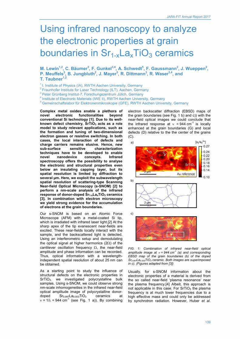
JARA-FIT Annual Report 2017
139
Using infrared nanoscopy to analyze the electronic properties at grain boundaries in Sr1-xLaxTiO3 ceramics M. Lewin1,2, C. Bäumer3, F. Gunkel3,4, A. Schwedt5, F. Gaussmann2, J. Wueppen2, P. Meuffels3, B. Jungbluth2, J. Mayer5, R. Dittmann3, R. Waser3,4, and T. Taubner1,2 1 I. Institute of Physics (IA), RWTH Aachen University, Germany 2 Fraunhofer Institute for Laser Technology (ILT), Aachen, Germany 3 Peter Grünberg Institut-7, Forschungszentrum Jülich, Germany 4 Institute of Electronic Materials (IWE II), RWTH Aachen University, Germany 5 Gemeinschaftslabor für Elektronenmikroskopie (GFE), RWTH Aachen University, Germany Complex metal oxides enable a plethora of novel electronic functionalities beyond conventional Si technology [1]. Due to its well-known defect chemistry, SrTiO3 acts as a role model to study relevant applications, such as the formation and tuning of two-dimensional electron gasses or resistive switching. In both cases, the local interaction of defects and charge carriers remains elusive. Hence, new sub-surface sensitive characterization techniques have to be developed to enable novel nanodevice concepts. Infrared spectroscopy offers the possibility to analyse the electronic and structural properties even below an insulating capping layer, but its spatial resolution is limited by diffraction to several µm. Here, we exploit the subwavelength spatial resolution of scattering-type Scanning Near-field Optical Microscopy (s-SNOM) [2] to perform a nm-scale analysis of the infrared response of donor-doped Sr1-xLaxTiO3 ceramics [3]. In combination with electron microscopy we yield strong evidence for the accumulation of electrons at the grain boundaries.
Our s-SNOM is based on an Atomic Force Microscope (AFM) with a metal-coated Si tip, which is irradiated with infrared laser light.[2] At the sharp apex of the tip evanescent near-fields are excited. These near-fields locally interact with the sample, and the backscattered light is detected. Using an interferometric setup and demodulating the optical signal at higher harmonics (2Ω) of the cantilever oscillation frequency Ω, the near-field amplitude and phase information can be recorded. Thus, optical information with a wavelength-independent spatial resolution of about 25 nm can be obtained.
As a starting point to study the influence of structural defects on the electronic properties in SrTiO3, we investigated polycrystalline bulk samples. Using s-SNOM, we could observe strong nm-scale inhomogeneities in the infrared near-field optical amplitude image of polycrystalline donor-doped Sr0.997La0.003TiO3 ceramics at ν = 1/λ = 944 cm-1 (see Fig. 1 a)). By combining
electron backscatter diffraction (EBSD) maps of the grain boundaries (see Fig. 1 b) and c)) with the near-field optical images we could conclude that the infrared response at ν = 944 cm-1 is locally enhanced at the grain boundaries (G) and local defects (D) relative to the the center of the grains (C).
FIG. 1: Combination of infrared near-field optical amplitude image at ν = 944 cm-1 (a) and corresponding EBSD map of the grain boundaries (b) of the doped Sr0.997La0.003TiO3 ceramic. Both images are superimposed in c). (Figures adapted from [3])
Usually, for s-SNOM information about the electronic properties of a material is derived from the so called near-field ‘plasma resonance’ near the plasma frequency.[4] Albeit, this approach is not applicable in this case. For SrTiO3 the plasma frequency is at much lower frequencies due to a high effective mass and could only be addressed by synchrotron radiation. However, Huber et al.

JARA-FIT Annual Report 2017
140
showed that the phonon near-field resonance is in principle also sensitive to electronic variations.[5] In combination with a home-built long-wavelength broadband laser system, we perform a detailed spectroscopic analysis (λ = 7 – 18 μm) of the influence of free charge carriers on the near-field phonon resonance in SrTiO3 at λ = 15 μm. Thus, we demonstrate how plasmon-phonon coupling[5] can be exploited, to quantify the electronic properties of SrTiO3 from an analysis of its phonon near-field resonance with a table-top light source.
In Fig. 2 a) a high resolution near-field optical amplitude image of the region marked by a white rectangle in Fig. 1 c) is presented. By correlating the near-field information to the EBSD map of grain boundaries (marked in blue) infrared near-field spectra from the center of the grain ‘C’, a local defect ‘D’ and a single grain boundary ‘G’ could be studied (Fig. 2 b)).
FIG. 2: nm-scale infrared near-field spectroscopic analysis of the doped Sr0.997La0.003TiO3 ceramic. a) High resolution near-field optical amplitude image of the region marked in Fig. 1 c) with a white rectangle at ν = 944 cm-1. The grain boundaries are marked in blue. b) Analysis of near-field spectra from the center of a grain ‘C’, a local defect ‘D’ and a grain boundary ‘G’. The Finite Dipole Model6 was used to adjust charge carrier density N, mobility µ and the high frequency offset e∞ to best fit the experimental spectra. (Figures adapted from [3])
We observe a strong damping of the phonon resonance (νres ≈ 680 cm-1) at the local defect and the grain boundary compared to the center of the grain. At the same time the near-field amplitude at high frequencies is significantly increased at the grain boundary and the defect compared to the center of the grain. Especially, due to the strong contrast outside the phonon resonance, we ascribe the damping of the phonon resonance to the influence of additional charge carriers. We succeeded to extract the local electronic properties by using the Finite Dipole Model6 and adjusting the charge carrier density N, the mobility µ and the high frequency offset e∞ to best fit the near-field spectra experimentally observed. The nominal doping of the ceramic corresponds to a charge carrier concentration of Ndop ≈ 5×1019 cm-3. However, we observe an increase of the charge carrier densities by a factor of two (four) at the grain boundary (at a local defect), relative to the center of the grains. At the same time the mobility maintains a relative constant value of about µ = 5 cm²/Vs, which is in accordance with literature values at room temperature.[7] Our results can be explained by defect chemical calculations taking into account the low oxygen partial pressure during the preparation of the ceramic sample. Due to a suppressed formation of Sr vacancies the trapping of oxygen vacancies at the grain boundaries can result in a local accumulation of electrons.
With this new kind of analysis, we make s-SNOM accessible for an entirely new field of analysis of functional materials and a broad scientific community working on complex oxides and oxide electronic nanodevices. Our proof-of-principle imposes an important step for future in-operando, nm-scale mapping of defects and charge carriers in technologically relevant applications of SrTiO3: Redox-based resistive random access memory (ReRAM), formation and tuning of two-dimensional electron gasses.
[1] H. Takagi and H. Y. Hwang, Science 327, 1601 (2010).
[2] F. Keilmann and R. Hillenbrand, Philos. Trans. R. Soc. 362, 787 (2004).
[3] M. Lewin, C. Baeumer, F. Gunkel, A. Schwedt, F. Gaussmann, J. Wueppen, P. Meuffels, B. Jungbluth, J. Mayer, R. Dittmann, R. Waser, and T. Taubner, Adv. Func. Mater. 28, 1802834 (2018)
[4] R. Ukropec, F. Haas, L. Jung, B. Hauer, H. Lüth, D. Grützmacher, T. Taubner, H. Hardtdegen, and T. Schäpers., JARA-FIT Annual Report 2016, 43 (2017)
[5] A. Huber, N. Ocelic, T. Taubner, and R. Hillenbrand, Nano Lett. 6, 774 (2006)
[6] A. Cvitkovic, N. Ocelic, and R. Hillenbrand, Opt. Express 15, 8550 (2007)
[7] R. Moos and K. H. Härdtl, J. Appl. Phys. 80, 393 (1996).

JARA-FIT Annual Report 2017
141
1S1R-based Connection-Centric Architecture for the Realization of 2-ary Logic Functions A. Heittmann and T.G. Noll Chair of Integrated Digital Systems and Circuit Design
A neuromorphic architecture based on Binary Associative memories and nanoelectronic resistive switches is proposed for the realization of arbitrary logic/arithmetic functions. Subsets of non-trivial code sets based on error detecting 2-out-of-n-codes are thoroughly used to encode operands, results, and intermediate states in order to enhance the circuit reliability by mitigating the impact of device variability. 2-ary functions can be implemented by cascading a mixer memory, a correlator memory, and a response memory. Reorganization of connection matrices by stochastic optimization results in a significant circuit compaction with the aim to minimize the overall number of active amplifiers. For various exemplary functions parameters of optimized architectures are reported.
Emerging passive nanoelectronic devices such as resistive switches (RS) [1] progressively proof to be very efficient in terms of area occupation at the device level. For many material systems RSs can be realized with the smallest possible footprint, i.e. an area occupation of 4F2 (F: lithographic feature size). While RS could turn out as effective successors for established memory devices by now, their application to realize logic functions is at least debatable. Here, typical concepts assume RS either to act as surrogate for standard devices within (established) fundamental logic gates [3], or to emulate leastwise the Boolean characteristics of standard logic gates [4]. In both cases, the fan-in of the gates remains comparatively low and only few RS devices contribute to a dedicated gate implementation. Both approaches show significant drawbacks:
• Amplification of inner signals with active devices becomes necessary for each gate.
• There is only a limited applicability of gates with large fan-in.
• Restricted options to improve the gate and circuit reliability at the circuit level.
In order to obviate or simplify these restrictions we propose to shift the circuit design paradigm from a gate-centric view to a connection-centric view. Here, the binary neural associative memories (BiNAMs) concept [2] becomes interesting for the implementation of arbitrary logic functions. Due to the regular matrix architecture of BiNAMs, emerging memory structures (cf. Fig.1) can be used for a circuit implementation. With respect to
nanoscaled RS, it is necessary to provide two distinctive resistive states for a memory cell to be used in a BiNAM: a so-called low-resistive-state (LRS) and a sufficiently large high-resistive-state (HRS). Under the assumption, that the electrical behavior of nanoscaled devices becomes unreliable, the following measures are taken into account in order to mitigate the impact of device variability [7,8]:
• Maximization of internal signal margins by the choice m=2.
• Standardized comparator (amplifier) design with uniform trigger threshold.
• Programming of connection weights by the write-verify methodology.
FIG 1: Elements of a memory architecture. a) exemplary I/V characteristics of a selector device [6]. b) Memory cell, composed of a selector S connected to a word line WL and an RS connected to a bit line BL. A HRS isolates WL and BL while a LRS establishes an unidirectional connection between WL and BL. c) bit line architecture and current summation.
In principle, m-out-of-n-codes can detect all unidirectional errors [5] and all 1-bit bidirectional errors as well. Generally, a function is considered as a mapping of r independent operands (arguments) to a functional result. Multivariate (r-ary) functions can be mapped on a hierarchical tree including monadic and bivariate operations only. Subsequently, an arbitrary bivariate operation Y=F(A,B) is considered which involves two operands A and B. A and B can take on symbols from a given (finite) code set C encoding states using 2-out-of-n codes. It has been shown in [8] that any function F can be realized by a particular bivariate mixing operation A⊗B∈C2→D∈CD (realized by Matrix M0), a so-called monadic correlation operation D→R∈CR (by
S
S
S
S
RL
YAθ
D
D
D
D…
VBL
BL
X0=1
X1=1
X2=0
X3=0
I0
I1
I2 ~ 0
I3 ~ 0
IBL=Σ Ij
VR
VR
0V
0V
b)
+
+
+
+
SIS
a)
10-10
0 1.0 2.0-1.0-2.0
10-8
10-6
10-4
10-2
VS[V]
|IS[A]|
VRS RS
BL
WL
VonVoff
Ioff
Ion
VS
Ion/Ioff ~ 104
WLBL
WL
LRS
HRS
BL
WL
VR
c)

JARA-FIT Annual Report 2017
142
M1),and a monadic response operation R→Y∈CY (by M2), cf. Fig.2a. A particular set CX (X=D, R, or Y) holds 2-out-of-NX codes which is used for encoding states of the operand X.
FIG. 2: a) 3-layered BiNAM-architecture for a connection-centric implementation of Y=F(A,B), b) example mapping with 3 pairs (X(k) ,Y(k))
The appropriate code sets CX are found by stochastic optimization which is driven by dedicated cost functions, see [8] for details. Once the sets are determined, the connections between word lines and bit lines can be set; for given binary vectors X(h)→Y(h), h=1..NM connections are defined by the clipped Hebbian synaptic rule [1,7,8]
qjpiYXc hi
hj
N
hij
M
..1..1)()(
1
==⋅= ∨=
(1)
In (1) Xj(h) denotes the (binary) state of the j-th
component in the binary vector X(h), Yi(h) the state
of the i-th component in the binary vector Y(h), NM the total number of pairs (X(h),Y(h)), and “∨” the logical OR function. A connection between a particular word line j and a bit line i exists if cij =1 (LRS) holds.
The mapping of a given input pattern (or symbol) X to an output pattern (or symbol) Y is realized by determining a sum Si for any bit line i=1...p. Si is compared with a given threshold θ which results in a derived state for the output bit Yi
∑∑ ===⋅=
11 jX ijq
j ijji ccXS , θ≥⇔= ii SY 1 (2)
Here, the sum (2) is implemented by a Kirchhoff adder [7,8].
For the evaluation of the proposed optimization [7,8] the parameters n=8 and z=|CAB|=8 were chosen representing 3 bit per symbol. This particular choice of parameters allows for the optimization of architectural parameters with reasonable effort. A selected set CAB realizes a true subset of C which allows for different implementations of M0 with different sizes ND ranging from ND,min=16 up to ND,max=32. Several 2-ary arithmetic functions (cf. Table I) were examined. Two different options were examined for the optimization of M0. Option 1 (blue) represents a cost function which is based on the comparator count ND (the “standard cost function”), option 2 (red) represents the proposed accumulated class-specific-word-line-coverage [8]. For ND,min ≤ ND ≤ND,max and both cost functions various realizations of M0 were generated using the stochastic optimization approach.
Table I: Comparison of architectural parameters obtained for option 1 (blue, standard) and option 2 (red, word line coverage)
While the optimization of M0 for option 1 was relatively straight-forward (i.e. the optimization loop immediately stops as soon as the target value for ND was obtained), T= 2x10⁶ iteration were used to obtain a stable cost-minimal solution of M0 for given F and option 2. Afterwards, M1/M2 were optimized based on the various realizations of M0 using the count NR as single cost function. For all given examples, also the size of CR was reduced which demonstrates the ability of M1 to represent correlations between various input patterns that map to the same output pattern. Clearly, the option 2 demonstrates a higher optimization potential. It is noteworthy, that for both options the rate of improvement significantly decreases as soon as the value of pon (i.e. the percentage of realized connections in relation to the matrix size) for matrix M2 reaches 50%. This seems to be in accordance with the theoretical results presented in [2] which state that for sparsely coded patterns the BiNAM reaches its storage capacity limit at pon=0.5. Clearly, as soon as the full capacity of M2 is used up, further optimizations are unlikely in the average. The value of pon for matrix M1 is smaller than 50% which indicates a certain amount of free memory space which might be due to sub-optimal code sets given by CD with respect to CR. In particular, the overall comparator count NA=NR+ND appears to be minimal for a specific ND,min. Interestingly, the optimal value for NA is significantly lower than the size of the input space z2=64, which indicates that the required overall complexity in terms of word lines is less than that of a plain look-up-table. This result has been verified for all examined functions, cf. Table I. The factor e=NA/z2 is significantly smaller than 1.0 in every case.
[1] R. Waser, R. Dittmann, G. Staikov, and K. Szot, Adv. Mater. 21, 2632 (2009)
[2] G. Palm, Biol. Cybernetics 36, 19 (1980) [3] P.-E. Gaillardon et al., VLSI-SoC 2012, p. 94 (2012) [4] A. Siemon et al., ISCAS 2015,p. 1338 (2015) [5] P. Lala, “Self-checking and Fault-Tolerant Digital
Design”, 1st. Edition, Morgan Kaufmann, (2000) [6] R. Aluguri and T. Y. Tseng, IEEE Journal of the
Electron Devices Society 4 (5), 294 (2016) [7] A.Heittmann and T.G.Noll, IEEE/ACM Nanoarch’17,
Newport (2017) [8] A.Heittmann and T.G.Noll,DATE’18, Desden (2018)
… …GA
A B
D
Y = F(A,B)
…
……
R
GB GD
GR
GY
M1
M2
θ =2
M0ND
11 NR
1NY
a) b)
Y(1)
Y(2)
Y(3)
X(1) X(2) X(3)
θ
MG1
G2
0
i
j
1 p1
q
cij=1j
i1
1
0 101 0 0 1 00 1 0 0
10001
01010
01001
Pon,M1 Pon.M2 NR+NDND,opt |CR| e|CY|(A + B) mod z
(A x B) mod z
((A x B)/z) mod z
MAX(A,B)
MIN(A,B)
COMPARE(A,B)
Carry-lookahead
8
8
7
8
8
3
3
20 4423 55
68.8%3861
32.7% 55.7%25.9% 55.9% 85.9%
„<“ „=“ „>“
„D“ „G“ „P“
Y=F(A,B) Pon,M0|CD|6464
16 3219 50
50.0%2653
46.1% 63.3%27.8% 54.4% 78.1%
4864
18 4121 46
64.1%3448
31.1% 53.2%29.1% 54.0% 71.9%
5364
20 4120 44
64.1%3146
36.7% 53.6%32.7% 59.4% 68.8%
6462
20 4316 45
67.2%4352
32.8% 56.5%35.7% 53.4% 70.3%
5664
16 2816 33
43.8%1533
57.3% 54.1%41.2% 63.2% 51.6%
4840
18 3018 34
46.9%2034
48.7% 53.4%42.3% 59.0% 53.1%
4250
15.0%15.3%17.2%17.4%16.7%16.4%15.0%16.8%15.6%18.8%17.1%19.2%17.6%18.0%
„0“ - „7“
„0“ - „7“
„0“ - „6“
„0“ - „7“
„0“ - „7“

JARA-FIT Annual Report 2017
143
Publications

JARA-FIT Annual Report 2017
144
Adly N., Feng L. Y., Krause K. J., Mayer D., Yakushenko A., Offenhausser A., and Wolfrum B. Flexible Microgap Electrodes by Direct Inkjet Printing for Biosensing Application Advanced Biosystems 1, 1600016 (2017) Adly N. Y., Bachmann B., Krause K. J., Offenhausser A., Wolfrum B., and Yakushenko A. Three-dimensional inkjet-printed redox cycling sensor RSC Advances 7, 5473 (2017) Afanas'ev V. V., Schulte-Braucks C., Wirths S., Schubert J., and Buca D. Oxidation-induced electron barrier enhancement at interfaces of Ge-based semiconductors (Ge, Ge1-x Snx, SiyGe1-x-y Snx) with Al2O3 Microelectronic Engineering 178, 141 (2017) Alagha S., Heedt S., Vakulov D., Mohammadbeigi F., Kumar E. S., Schapers T., Isheim D., Watkins S. P., and Kavanagh K. L. Electrical properties of lightly Ga-doped ZnO nanowires Semiconductor Science and Technology 32, 125010 (2017) Almudever C. G., Lao L., Fu X., Khammassi N., Ashraf I., Iorga D., Varsamopoulos S., Eichler C., Wallraff A., Geck L., Kruth A., Knoch J., Bluhm H., and Bertels K. The Engineering Challenges in Quantum Computing Proceedings of the 2017 Design, Automation & Test in Europe Conference & Exhibition (Date), 836 (2017) Andra M., Dvorak F., Vorokhta M., Nemsak S., Matolin V., Schneider C. M., Dittmann R., Gunkel F., Mueller D. N., and Waser R. Oxygen partial pressure dependence of surface space charge formation in donor-doped SrTiO3 APL Materials 5, 056106 (2017) Ansari M. H. Entropy production in a photovoltaic cell Physical Review B 95, 174302 (2017) Arndt B., Borgatti F., Offi F., Phillips M., Parreira P., Meiners T., Menzel S., Skaja K., Panaccione G., MacLaren D. A., Waser R., and Dittmann R. Spectroscopic Indications of Tunnel Barrier Charging as the Switching Mechanism in Memristive Devices Advanced Functional Materials 27, 1702282 (2017) Assali S., Dijkstra A., Li A., Koelling S., Verheijen M. A., Gagliano L., von den Driesch N., Buca D., Koenraad P. M., Haverkort J. E. M., and Bakkers E. P. A. M. Growth and Optical Properties of Direct Band Gap Ge/Ge0.87Sn0.13 Core/Shell Nanowire Arrays Nano Letters 17, 1538 (2017) Aussen S., Hardtdegen A., Skaja K., and Hoffmann-Eifert S. Interfaces Formed by ALD Metal Oxide Growth on Metal Layers Atomic Layer Deposition Applications 13 80, 87 (2017) Avila J., Chen C., Arango Y. C., Huang L. B., Grutzmacher D., Luth H., Lu J. G., Schapers T., and Asensio M. C. Nano-Angle Resolved Photoemission Spectroscopy on Topological insulator Sb2Te3 nanowires responsible of quantum transport Proceedings of the 33rd International Conference on the Physics of Semiconductors 864, 012041 (2017) Babcock E., Salhi Z., Gainov R., Woracek R., Soltner H., Pistel P., Beule F., Bussmann K., Heynen A., Kaammerling H., Suxdorf F., Strobl M., Russina M., Voigt J., and Ioffe A. Recent on-beam tests of wide angle neutron polarization analysis with a 3He spin filter: Magic PASTIS on V20 at HZB J. Phys.: Conference Series, Proceedings of the International Conference on Polarised Neutrons for Condensed Matter Investigations (PNCMI 2016) 862, 012002 (2017) Babcock E., Salhi Z., Kentzinger E., Mattauch S., and Ioffe A. Discussion on data correction for Polarization Analysis with a 3He spin filter analyzer J. Phys.: Conference Series, Proceedings of the International Conference on Polarised Neutrons for Condensed Matter Investigations (PNCMI 2016) 862, 012001 (2017)

JARA-FIT Annual Report 2017
145
Baby A., Gruenewald M., Zwick C., Otto F., Forker R., van Straaten G., Franke M., Stadtmuller B., Kumpf C., Brivio G. P., Fratesi G., Fritz T., and Zojer E. Fully Atomistic Understanding of the Electronic and Optical Properties of a Prototypical Doped Charge-Transfer Interface ACS Nano 11, 10495 (2017) Backes D., Huang D. H., Mansell R., Lanius M., Kampmeier J., Ritchie D., Mussler G., Gumbs G., Grutzmacher D., and Narayan V. Disentangling surface and bulk transport in topological-insulator p-n junctions Physical Review B 96, 125125 (2017) Baeumer C., Valenta R., Schmitz C., Locatelli A., Mentes T. O., Rogers S. P., Sala A., Raab N., Nemsak S., Shim M., Schneider C. M., Menzel S., Waser R., and Dittmann R. Subfilamentary Networks Cause Cycle-to-Cycle Variability in Memristive Devices ACS Nano 11, 6921 (2017) Bahrenberg L., Danylyuk S., Brose S., Pollentier I., Timmermans M., Gallagher E., Stollenwerk J., and Loosen P. Characterization of pellicle membranes by lab-based spectroscopic reflectance and transmittance measurements in the extreme ultraviolet Proceedings of the International Conference on Extreme Ultraviolet Lithography 2017 10450, 104501l (2017) Bahuguna J., Tetzlaff T., Kumar A., Hellgren Kotaleski J., Morrison A. Homologous basal ganglia network models in physiological and parkinsonian conditions. Frontiers in Computational Neuroscience 11, 79 (2017) Banszerus L., Janssen H., Otto M., Epping A., Taniguchi T., Watanabe K., Beschoten B., Neumaier D., and Stampfer C. Identifying suitable substrates for high-quality graphene-based heterostructures 2d Materials 4, 025030 (2017) Banszerus L., Watanabe K., Taniguchi T., Beschoten B., and Stampfer C. Dry transfer of CVD graphene using MoS2-based stamps Physica Status Solidi-Rapid Research Letters 11, 1700136 (2017) Battiato M., Aguilera I., and Sanchez-Barriga J. Generalized GW plus Boltzmann Approach for the Description of Ultrafast Electron Dynamics in Topological Insulators Materials 10, 810 (2017) Becker J., Kohler T., Tiegel A. C., Manmana S. R., Wessel S., and Honecker A. Finite-temperature dynamics and thermal intraband magnon scattering in Haldane spin-one chains Physical Review B 96, 060403 (2017) Beschnitt S. and De Souza R. A. Impurity diffusion of Hf and Zr in Gd-doped CeO2 Solid State Ionics 305, 23 (2017) Bindel J. R., Ulrich J., Liebmann M., and Morgenstern M. Probing the Nodal Structure of Landau Level Wave Functions in Real Space Physical Review Letters 118, 016803 (2017) Biniskos N., Raymond S., Schmalzl K., Schneidewind A., Voigt J., Georgii R., Hering P., Persson J., Friese K., and Bruckel T. Spin dynamics of the magnetocaloric compound MnFe4Si3 Physical Review B 96, 104407 (2017) Biswas A., Luong G. V., Chowdhury M. F., Alper C., Zhao Q. T., Udrea F., Mantl S., and Lonescu A. M. Benchmarking of Homojunction Strained-Si NW Tunnel FETs for Basic Analog Functions Ieee Transactions on Electron Devices 64, 1441 (2017) Boggild P., Caridad J. M., Stampfer C., Calogero G., Papior N. R., and Brandbyge M. A two-dimensional Dirac fermion microscope Nature Communications 8, 15783 (2017)

JARA-FIT Annual Report 2017
146
Borghardt S., Winkler F., Zanolli Z., Verstraete M. J., Barthel J., Tavabi A. H., Dunin-Borkowski R. E., and Kardynal B. E. Quantitative Agreement between Electron-Optical Phase Images of WSe2 and Simulations Based on Electrostatic Potentials that Include Bonding Effects Physical Review Letters 118, 086101 (2017) Bosco S. and DiVincenzo D. P. Nonreciprocal quantum Hall devices with driven edge magnetoplasmons in two-dimensional materials Physical Review B 95, 195317 (2017) Bosco S., Haupt F., and DiVincenzo D. P. Self-Impedance-Matched Hall-Effect Gyrators and Circulators Physical Review Applied 7, 024030 (2017) Bottger U. and Waser R. Interaction between depolarization effects, interface layer, and fatigue behavior in PZT thin film capacitors Journal of Applied Physics 122, 024105 (2017) Bouaziz J., Dias M. D. S., Ziane A., Benakki M., Blugel S., and Lounis S. Chiral magnetism of magnetic adatoms generated by Rashba electrons New Journal of Physics 19, 023010 (2017) Breuckmann N. P., Duivenvoorden K., Michels D., and Terhal B. M. Local Decoders for the 2d and 4d Toric Code Quantum Information & Computation 17, 181 (2017) Breuckmann N. P., Vuillot C., Campbell E., Krishna A., and Terhal B. M. Hyperbolic and semi-hyperbolic surface codes for quantum storage Quantum Science and Technology 2, 035007 (2017) Brose S., Danylyuk S., Bahrenberg L., Lebert R., Loosen P., and Juschkin L. Optimized phase-shifting masks for high-resolution resist patterning by interference lithography Proceedings of the International Conference on Extreme Ultraviolet Lithography 2017 10450, 104502a (2017) Brulke C., Heepenstrick T., Humberg N., Krieger I., Sokolowski M., Weiss S., Tautz F. S., and Soubatch S. Long Vertical Distance Bonding of the Hexagonal Boron Nitride Monolayer on the Cu(111) Surface Journal of Physical Chemistry C 121, 23964 (2017) Buhl P. M., Freimuth F., Blugel S., and Mokrousov Y. Topological spin Hall effect in antiferromagnetic skyrmions Physica Status Solidi-Rapid Research Letters 11, 1700007 (2017) Bussmann J., Odstrcil M., Teramoto Y., and Juschkin L. Ptychographic imaging with partially coherent plasma EUV sources Advanced Optical Technologies 6, 459 (2017) Cai B., Schwarzkopf J., Feldt C., Sellmann J., Markurt T., and Wordenweber R. Combined impact of strain and stoichiometry on the structural and ferroelectric properties of epitaxially grown Na1+xNbO3+δ film on (110) NdGaO3 Physical Review B 95, 184108 (2017) Campbell E. T., Terhal B. M., and Vuillot C. Roads towards fault-tolerant universal quantum computation Nature 549, 172 (2017) Celano U., de Beeck J. O., Clima S., Luebben M., Koenraad P. M., Goux L., Valov I., and Vandervorst W. Direct Probing of the Dielectric Scavenging-Layer Interface in Oxide Filamentary-Based Valence Change Memory ACS Applied Materials & Interfaces 9, 10820 (2017) Chen C., Jost P., Volker H., Kaminski M., Wirtssohn M., Engelmann U., Kruger K., Schlich F., Schlockermann C., Lobo R. P. S. M., and Wuttig M. Dielectric properties of amorphous phase-change materials Physical Review B 95, 094111 (2017)

JARA-FIT Annual Report 2017
147
Chen X. Z., Feng J. F., Wang Z. C., Zhang J., Zhong X. Y., Song C., Jin L., Zhang B., Li F., Jiang M., Tan Y. Z., Zhou X. J., Shi G. Y., Zhou X. F., Han X. D., Mao S. C., Chen Y. H., Han X. F., and Pan F. Tunneling anisotropic magnetoresistance driven by magnetic phase transition Nature Communications 8, 449 (2017) Cho D. Y., Luebben M., Wiefels S., Lee K. S., and Valov I. Interfacial Metal-Oxide Interactions in Resistive Switching Memories ACS Applied Materials & Interfaces 9, 19287 (2017) Chugreeva O. and Melcher C. Vortices in a stochastic parabolic Ginzburg-Landau equation Stochastics and Partial Differential Equations-Analysis and Computations 5, 113 (2017) Ciani A. and DiVincenzo D. P. Three-qubit direct dispersive parity measurement with tunable coupling qubits Physical Review B 96, 214511 (2017) Cooper D., Baeumer C., Bernier N., Marchewka A., La Torre C., Dunin-Borkowski R. E., Menzel S., Waser R., and Dittmann R. Anomalous Resistance Hysteresis in Oxide ReRAM: Oxygen Evolution and Reincorporation Revealed by In Situ TEM Advanced Materials 29, 1700212 (2017) Cui S. X., Gottesman D., and Krishna A. Diagonal gates in the Clifford hierarchy Physical Review A 95, 012329 (2017) Danopoulos A. A., Braunstein P., Monakhov K. Y., van Leusen J., Kogerler P., Clemancey M., Latour J. M., Benayad A., Tromp M., Rezabal E., and Frison G. Heteroleptic, two-coordinate [M(NHC)N(SiMe3)2] (M = Co, Fe) complexes: synthesis, reactivity and magnetism rationalized by an unexpected metal oxidation state Dalton Transactions 46, 1163 (2017) Dauber J., Oellers M., Venn F., Epping A., Watanabe K., Taniguchi T., Hassler F., and Stampfer C. Aharonov-Bohm oscillations and magnetic focusing in ballistic graphene rings Physical Review B 96, 205407 (2017) Degtyarev V. E., Khazanova S. V., and Demarina N. V. Features of electron gas in InAs nanowires imposed by interplay between nanowire geometry, doping and surface states Scientific Reports 7, 3411 (2017) de la Pena D. S., Lichtenstein J., and Honerkamp C. Competing electronic instabilities of extended Hubbard models on the honeycomb lattice: A functional renormalization group calculation with high-wave-vector resolution Physical Review B 95, 085143 (2017) de la Pena D. S., Lichtenstein J., Honerkamp C., and Scherer M. M. Antiferromagnetism and competing charge instabilities of electrons in strained graphene from Coulomb interactions Physical Review B 96, 205155 (2017) De Souza R. A. Limits to the rate of oxygen transport in mixed-conducting oxides Journal of Materials Chemistry A 5, 20334 (2017) Dias M. D. and Lounis S. Insights into the orbital magnetism of noncollinear magnetic systems Proceedings of Spintronics X 10357, 103572a (2017) DiVincenzo D. P. Scientists and citizens: getting to quantum technologies Ethics and Information Technology 19, 247 (2017) Doring L. and Melcher C. Compactness results for static and dynamic chiral skyrmions near the conformal limit Calculus of Variations and Partial Differential Equations 56, 60 (2017)

JARA-FIT Annual Report 2017
148
dos Santos F. J., Dias M. D., and Lounis S. First-principles investigation of spin-wave dispersions in surface-reconstructed Co thin films on W(110) Physical Review B 95, 134408 (2017) Drissi L. B., Ramadan F. Z., and Lounis S. Halogenation of SiC for band-gap engineering and excitonic functionalization Journal of Physics-Condensed Matter 29, 455001 (2017) Drögeler M., Banszerus L., Volmer F., Taniguchi T., Watanabe K., Beschoten B., and Stampfer C. Dry-transferred CVD graphene for inverted spin valve devices Applied Physics Letters 111, 152402 (2017) Drögeler M., Volmer F., Stampfer C., and Beschoten B. Simulations on the Influence of Spatially Varying Spin Transport Parameters on the Measured Spin Lifetime in Graphene Non-Local Spin Valves Physica Status Solidi B-Basic Solid State Physics 254, 1700293 (2017) Du H. C., Jia C. L., Koehl A., Barthel J., Dittmann R., Waser R., and Mayer J. Nanosized Conducting Filaments Formed by Atomic-Scale Defects in Redox-Based Resistive Switching Memories Chemistry of Materials 29, 3164 (2017) Duivenvoorden K., Iqbal M., Haegeman J., Verstraete F., and Schuch N. Entanglement phases as holographic duals of anyon condensates Physical Review B 95, 235119 (2017) Duivenvoorden K., Terhal B. M., and Weigand D. Single-mode displacement sensor Physical Review A 95, 012305 (2017) Dunin-Borkowski R. E., Mayer J., and Tillmann K. Introduction to a special issue on Frontiers of Aberration Corrected Electron Microscopy in honour of Robert Sinclair and Nestor J. Zaluzec on the occasion of their 70th and 65th birthdays Ultramicroscopy 176, 1 (2017) Ebeling R., Tsukamoto S., Dirksen E., Caciuc V., Muller T. J. J., Atodiresei N., and Karthauser S. Imaging Individual Molecular-Like Orbitals of a Non-Planar Naphthalene Diimide on Pt(111): A Combined STM and DFT Study Journal of Physical Chemistry C 121, 26916 (2017) Engels J., Griesche D., Waser R., and Schneller T. Thin film proton conducting membranes for micro-solid oxide fuel cells by chemical solution deposition Thin Solid Films 636, 446 (2017) Esat T., Friedrich R., Matthes F., Caciuc V., Atodiresei N., Blugel S., Burgler D. E., Tautz F. S., and Schneider C. M. Quantum interference effects in molecular spin hybrids Physical Review B 95, 094409 (2017) Eschbach M., Lanius M., Niu C. W., Mlynczak E., Gospodaric P., Kellner J., Schuffelgen P., Gehlmann M., Doring S., Neumann E., Luysberg M., Mussler G., Plucinski L., Morgenstern M., Grutzmacher D., Bihlmayer G., Blugel S., and Schneider C. M. Bi1Te1 is a dual topological insulator Nature Communications 8, 14976 (2017) Esser M. and Dronskowski R. Ab initio triangle maps for new insights into the crystal wave functions of carbon allotropes Carbon 123, 708 (2017) Esser M., Esser A. A., Proserpio D. M., and Dronskowski R. Bonding analyses of unconventional carbon allotropes Carbon 121, 154 (2017) Esser M., Maintz S., and Dronskowski R. Automated First-Principles Mapping for Phase-Change Materials Journal of Computational Chemistry 38, 620 (2017)

JARA-FIT Annual Report 2017
149
Farokhnejad A., Graef M., Horst F., Liu C., Zhao Q. T., Iniguez B., Lime F., and Kloes A. Compact Modeling of Intrinsic Capacitances in Double-Gate Tunnel-FETs Proceedings of the 2017 Joint International Eurosoi Workshop and International Conference on Ultimate Integration on Silicon (Eurosoi-UlLIS 2017), 140 (2017) Feld A., Koll R., Fruhner L. S., Krutyeva M., Pyckhout-Hintzen W., Weiss C., Heller H., Weimer A., Schmidtke C., Appavou M. S., Kentzinger E., Allgaier J., and Weller H. Nanocomposites of Highly Monodisperse Encapsulated Superparamagnetic Iron Oxide Nanocrystals Homogeneously Dispersed in a Poly(ethylene Oxide) Melt ACS Nano 11, 3767 (2017) Fiedler L., Naaijkens P., and Osborne T. J. Jones index, secret sharing and total quantum dimension New Journal of Physics 19, 023039 (2017) Finge T., Riederer F., Mueller M. R., Grap T., Kallis K., and Knoch J. Investigations on Field-Effect Transistors Based on Two-Dimensional Materials Annalen der Physik 529, 1700087 (2017) Fischer I. A., Berrier A., Hornung F., Oehme M., Zaumseil P., Capellini G., den Driesch N. V., Buca D., and Schulze J. Optical critical points of SixGe1-x-ySny alloys with high Si content Semiconductor Science and Technology 32, 124004 (2017) Flovik V., Qaiumzadeh A., Nandy A. K., Heo C., and Rasing T. Generation of single skyrmions by picosecond magnetic field pulses Physical Review B 96, 140411 (2017) Freimuth F., Blugel S., and Mokrousov Y. Chiral damping, chiral gyromagnetism, and current-induced torques in textured one-dimensional Rashba ferromagnets Physical Review B 96, 104418 (2017) Freimuth F., Blugel S., and Mokrousov Y. Relation of the Dzyaloshinskii-Moriya interaction to spin currents and to the spin-orbit field Physical Review B 96, 054403 (2017) Freimuth F., Blugel S., and Mokrousov Y. Geometrical contributions to the exchange constants: Free electrons with spin-orbit interaction Physical Review B 95, 184428 (2017) Freimuth F., Blugel S., and Mokrousov Y. Charge pumping driven by the laser-induced dynamics of the exchange splitting Physical Review B 95, 094434 (2017) Friedrich R., Caciuc V., Bihlmayer G., Atodiresei N., and Blugel S. Designing the Rashba spin texture by adsorption of inorganic molecules New Journal of Physics 19, 043017 (2017) Friedrich R., Caciuc V., Zimmermann B., Bihlmayer G., Atodiresei N., and Blugel S. Creating anisotropic spin-split surface states in momentum space by molecular adsorption Physical Review B 96, 085403 (2017) Fritz F., Westerstrom R., Kostanyan A., Schlesier C., Dreiser J., Watts B., Houben L., Luysberg M., Avdoshenko S. M., Popov A. A., Schneider C. M., and Meyer C. Nanoscale x-ray investigation of magnetic metallofullerene peapods Nanotechnology 28, 435703 (2017) Fukushima T., Katayama-Yoshida H., Sato K., Ogura M., Zeller R., and Dederichs P. H. Local Energies and Energy Fluctuations - Applied to the High Entropy Alloy CrFeCoNi Journal of the Physical Society of Japan 86, 114704 (2017) Funck C., Hoffmann-Eifert S., Lukas S., Waser R., and Menzel S. Design rules for threshold switches based on a field triggered thermal runaway mechanism Journal of Computational Electronics 16, 1175 (2017)

JARA-FIT Annual Report 2017
150
Gaudenzi R., Misiorny M., Burzuri E., Wegewijs M. R., and van der Zant H. S. J. Transport mirages in single-molecule devices Journal of Chemical Physics 146, 092330 (2017) Gehlmann M., Aguilera I., Bihlmayer G., Nemsak S., Nagler P., Gospodaric P., Zamborlini G., Eschbach M., Feyer V., Kronast F., Mlynczak E., Korn T., Plucinski L., Schuller C., Blugel S., and Schneider C. M. Direct Observation of the Band Gap Transition in Atomically Thin ReS2 Nano Letters 17, 5187 (2017) Georgi A., Nemes-Incze P., Carrillo-Bastos R., Faria D., Kusminskiy S. V., Zhai D. W., Schneider M., Subramaniam D., Mashoff T., Freitag N. M., Liebmann M., Pratzer M., Wirtz L., Woods C. R., Gorbachey R. V., Cao Y., Novoselov K. S., Sandier N., and Morgenstern M. Tuning the Pseudospin Polarization of Graphene by a Pseudomagnetic Field Nano Letters 17, 2240 (2017) Geranton G., Zimmermann B., Long N. H., Mavropoulos P., Blugel S., Freimuth F., and Mokrousov Y. Nonlocal fieldlike spin-orbit torques in Rashba systems: Ab initio study of a Ag2Bi-terminated Ag(111) film grown on a ferromagnetic Fe(110) substrate Physical Review B 95, 134449 (2017) Gity F., Ansari L., Lanius M., Schuffelgen P., Mussler G., Grutzmacher D., and Greer J. C. Reinventing solid state electronics: Harnessing quantum confinement in bismuth thin films Applied Physics Letters 110, 093111 (2017) Glass S., Schulte-Braucks C., Kibkalo L., Breuer U., Hartmann J. M., Buca D., Mantl S., and Zhao Q. T. Examination of a new SiGe/Si heterostructure TFET concept based on vertical tunneling Proceedings of the Fifth Berkeley Symposium on Energy Efficient Electronic Systems & Steep Transistors Workshop (E3S) (2017) Glass S., von den Driesch N., Strangio S., Schulte-Braucks C., Rieger T., Narimani K., Buca D., Mantl S., and Zhao Q. T. Experimental examination of tunneling paths in SiGe/Si gate-normal tunneling field-effect transistors Applied Physics Letters 111, 263504 (2017) Go D., Hanke J. P., Buhl P. M., Freimuth F., Bihlmayer G., Lee H. W., Mokrousov Y., and Blugel S. Toward surface orbitronics: giant orbital magnetism from the orbital Rashba effect at the surface of sp-metals Scientific Reports 7, 46742 (2017) Gobgen K. C., Steinberg S., and Dronskowski R. Revisiting the Si-Te System: SiTe2 Finally Found by Means of Experimental and Quantum-Chemical Techniques Inorganic Chemistry 56, 11398 (2017) Gonzalez S., Mathieu C., Copie O., Feyer V., Schneider C. M., and Barrett N. Room temperature 2D electron gas at the (001)-SrTiO3 surface Applied Physics Letters 111, 181601 (2017) Grap T., Riederer F., Gupta C., and Knoch J. Buried Multi-Gate InAs-Nanowire FETs Proceedings of the 47th European Solid-State Device Research Conference (ESSDERC), 82 (2017) Grellmann T., Mayer D., Offenhausser A., and Wordenweber R. Temperature-Dependent Electron Transport in Single Terphenyldithiol Molecules Journal of Physical Chemistry A 121, 2911 (2017) Gritti C., Raza S., Kadkhodazadeh S., Kardynal B., Malureanu R., Mortensen N. A., and Lavrinenko A. V. Broadband infrared absorption enhancement by electroless-deposited silver nanoparticles Nanophotonics 6, 289 (2017) Guimaraes F. S. M., Dias M. D., Bouaziz J., Costa A. T., Muniz R. B., and Lounis S. Dynamical amplification of magnetoresistances and Hall currents up to the THz regime Scientific Reports 7, 3686 (2017) Guimaraes F. S. M., Dias M. D., Schweflinghaus B., and Lounis S. Engineering elliptical spin-excitations by complex anisotropy fields in Fe adatoms and dimers on Cu(111) Physical Review B 96, 144401 (2017)

JARA-FIT Annual Report 2017
151
Gunkel F., Hoffmann-Eifert S., Heinen R. A., Christensen D. V., Chen Y. Z., Pryds N., Waser R., and Dittmann R. Thermodynamic Ground States of Complex Oxide Heterointerfaces ACS Applied Materials & Interfaces 9, 1086 (2017) Gunkel F., Jin L., Mueller D. N., Hausner C., Bick D. S., Jia C. L., Schneller T., Valov I., Waser R., and Dittmann R. Ordering and Phase Control in Epitaxial Double-Perovskite Catalysts for the Oxygen Evolution Reaction ACS Catalysis 7, 7029 (2017) Gusken N. A., Rieger T., Zellekens P., Bennemann B., Neumann E., Lepsa M. I., Schapers T., and Grutzmacher D. MBE growth of Al/InAs and Nb/InAs superconducting hybrid nanowire structures Nanoscale 9, 16735 (2017) Haas F., Zellekens P., Lepsa M., Rieger T., Grutzmacher D., Luth H., and Schapers T. Electron Interference in Hall Effect Measurements on GaAs/InAs Core/Shell Nanowires Nano Letters 17, 128 (2017) Haas F., Zellekens P., Wenz T., Demarina N., Rieger T., Lepsa M. I., Grutzmacher D., Luth H., and Schapers T. Anisotropic phase coherence in GaAs/InAs core/shell nanowires Nanotechnology 28, 445202 (2017) Hahne J., Dahmen D., Schuecker J., Frommer A., Bolten M., Helias M., Diesmann M. Integration of continuous-time dynamics in a spiking neural network simulator. Frontiers in Neuroinformatics 11, 34 (2017) Han Q. H., Gao A., Narimani K., Wang Y. L., Li T., Mantl S., and Zhao Q. T. Ultrathin Lateral Unidirectional Bipolar-Type Insulated-Gate Transistor as pH sensor Proceedings of the 47th European Solid-State Device Research Conference (ESSDERC), 268 (2017) Hanke J. P., Freimuth F., Blugel S., and Mokrousov Y. Prototypical topological orbital ferromagnet gamma-FeMn Scientific Reports 7, 41078 (2017) Hanke J. P., Freimuth F., Niu C. W., Blugel S., and Mokrousov Y. Mixed Weyl semimetals and low-dissipation magnetization control in insulators by spin-orbit torques Nature Communications 8, 1479 (2017) Heedt S., Ziani N. T., Crepin F., Prost W., Trellenkamp S., Schubert J., Grutzmacher D., Trauzettel B., and Schapers T. Signatures of interaction-induced helical gaps in nanowire quantum point contacts Nature Physics 13, 563 (2017) Heittmann A. and Noll T. G. Mixing Circuit Based on Neural Associative Memories and Nanoelectronic 1S1R Cells Proceedings of the IEEE/ACM International Symposium on Nanoscale Architectures (Nanoarch 2017), 119 (2017) Henneke C., Felter J., Schwarz D., Tautz F. S., and Kumpf C. Controlling the growth of multiple ordered heteromolecular phases by utilizing intermolecular repulsion Nature Materials 16, 628 (2017) Hensling F. V. E., Xu C. C., Gunkel F., and Dittmann R. Unraveling the enhanced Oxygen Vacancy Formation in Complex Oxides during Annealing and Growth Scientific Reports 7, 39953 (2017) Hermenau J., Ibanez-Azpiroz J., Hubner C., Sonntag A., Baxevanis B., Ton K. T., Steinbrecher M., Khajetoorians A. A., Dias M. D., Blugel S., Wiesendanger R., Lounis S., and Wiebe J. A gateway towards non-collinear spin processing using three-atom magnets with strong substrate coupling Nature Communications 8, 642 (2017) Herzog F., Hardtdegen H., Schapers T., Grundler D., and Wilde M. A. Experimental determination of Rashba and Dresselhaus parameters and g*- factor anisotropy via Shubnikov-de Haas oscillations New Journal of Physics 19, 103012 (2017)

JARA-FIT Annual Report 2017
152
Hess V., Friedrich R., Matthes F., Caciuc V., Atodiresei N., Burgler D. E., Blugel S., and Schneider C. M. Magnetic subunits within a single molecule-surface hybrid New Journal of Physics 19, 053016 (2017) Hoffmann M., Zimmermann B., Muller G. P., Schurhoff D., Kiselev N. S., Melcher C., and Blugel S. Antiskyrmions stabilized at interfaces by anisotropic Dzyaloshinskii-Moriya interactions Nature Communications 8, 308 (2017) Hollerer M., Luftner D., Hurdax P., Ules T., Soubatch S., Tautz F. S., Koller G., Puschnig P., Sterrer M., and Ramsey M. G. Charge Transfer and Orbital Level Alignment at Inorganic/Organic Interfaces: The Role of Dielectric Interlayers ACS Nano 11, 6252 (2017) Honerkamp C. Influence of hopping self-energy effects and quasiparticle degradation on the antiferromagnetic ordering in the bilayer honeycomb Hubbard model Physical Review B 96, 245134 (2017) Honerkamp C. Selfenergy Effect on the Magnetic Ordering Transition in the Mono- and Bilayer Honeycomb Hubbard Model Annalen der Physik 529, 1700044 (2017) Honerkamp C. Nematic and superconducting order in a three-band model for the iron superconductors Physica Status Solidi B-Basic Solid State Physics 254, 1600151 (2017) Horst F., Farokhnejad A., Graef M., Hosenfeld F., Luong G. V., Liu C., Zhao Q. T., Lime F., Iniguez B., and Kloes A. DC/AC Compact Modeling of TFETs for Circuit Simulation of Logic Cells Based on an Analytical Physics-Based Framework Proceedings of the 25th Austrochip Workshop on Microelectronics (Austrochip), 6 (2017) Horst F., Graef M., Hosenfeld F., Farokhnejad A., Luong G. V., Zhao Q. T., Iniguez B., and Kloes A. Static Noise Margin Analysis of 8T TFET SRAM Cells Using a 2D Compact Model Adapted to Measurement Data of Fabricated TFET Devices Proceedings of the Joint International Eurosoi Workshop and International Conference on Ultimate Integration on Silicon (Eurosoi-ULIS 2017), 39 (2017) Hosseinkhani A., Riwar R. P., Schoelkopf R. J., Glazman L. I., and Catelani G. Optimal Configurations for Normal-Metal Traps in Transmon Qubits Physical Review Applied 8, 064028 (2017) Hu J.T., Xiao Y.G., Tang H.T., Wang H.B., Wang Z.Q., Liu C.K., Zeng H., Huang Q.Z., Ren Y., Wang C.M, Zhang W., and Pan F. Tuning Li-Ion Diffusion in alpha-LiMn1-xFexPO4 Nanocrystals by Antisite Defects and Embedded beta-Phase for Advanced Li-Ion Batteries Nano Letters 17, 4934 (2017) Ibach H., Bocquet F. C., Sforzini J., Soubatch S., and Tautz F. S. Electron energy loss spectroscopy with parallel readout of energy and momentum Review of Scientific Instruments 88, 033903 (2017) Ibanez-Azpiroz J., Dias M. D., Blugel S., and Lounis S. Longitudinal and transverse spin relaxation times of magnetic single adatoms: An ab initio analysis Physical Review B 96, 144410 (2017) Ibanez-Azpiroz J., Dias M. D., Schweflinghaus B., Blugel S., and Lounis S. Tuning Paramagnetic Spin Excitations of Single Adatoms Physical Review Letters 119, 017203 (2017) Ippen T., Eppler JM., Plesser HE., and Diesmann M. Constructing neuronal network models in massively parallel environments. Frontiers in Neuroinformatics 11, 30 (2017)

JARA-FIT Annual Report 2017
153
Jafari A., Sergueev I., Bessas D., Klobes B., Roschin B. S., Asadchikov V. E., Alexeev P., Hartwig J., Chumakov A. I., Wille H. C., and Hermann R. P. Rocking curve imaging of high quality sapphire crystals in backscattering geometry Journal of Applied Physics 121, 044901 (2017) Jin C. M., Li Z. A., Kovacs A., Caron J., Zheng F. S., Rybakov F. N., Kiselev N. S., Du H. F., Blugel S., Tian M. L., Zhang Y. H., Farle M., and Dunin-Borkowski R. E. Control of morphology and formation of highly geometrically confined magnetic skyrmions Nature Communications 8, 15569 (2017) Jin L., Barthel J., Jia C. L., and Urban K. W. Atomic resolution imaging of YAlO3: Ce in the chromatic and spherical aberration corrected PICO electron microscope Ultramicroscopy 176, 99 (2017) Jin L., Xu P. X., Zeng Y., Lu L., Barthel J., Schulthess T., Dunin-Borkowski R. E., Wang H., and Jia C. L. Surface reconstructions and related local properties of a BiFeO3 thin film Scientific Reports 7, 39698 (2017) Jin W. T., Sun J. P., Ye G. Z., Xiao Y., Su Y., Schmalzl K., Nandi S., Bukowski Z., Guguchia Z., Feng E., Fu Z., and Cheng J. G. Hydrostatic pressure effects on the static magnetism in Eu(Fe0.925Co0.075)2As2 Scientific Reports 7, 3532 (2017) Josten E., Wetterskog E., Glavic A., Boesecke P., Feoktystov A., Brauweiler-Reuters E., Rucker U., Salazar-Alvarez G., Bruckel T., and Bergstrom L. Superlattice growth and rearrangement during evaporation-induced nanoparticle self-assembly Scientific Reports 7, 2802 (2017) Just S., Soltner H., Korte S., Cherepanov V., and Voigtlander B. Surface conductivity of Si(100) and Ge(100) surfaces determined from four-point transport measurements using an analytical N-layer conductance model Physical Review B 95, 075310 (2017) Kammermeier M., Wenk P., Schliemann J., Heedt S., Gerster T., and Schapers T. Magnetoconductance correction in zinc-blende semiconductor nanowires with spin-orbit coupling Physical Review B 96, 235302 (2017) Kampmann F., Scheuschner N., Terrés B., Jörger D., Stampfer C., and Maultzsch J. Raman Spectroscopy of Lithographically Defined Graphene Nanoribbons - Influence of Size and Defects Annalen der Physik 529, 1700167 (2017) Kellner J., Bihlmayer G., Deringer V. L., Liebmann M., Pauly C., Giussani A., Boschker J. E., Calarco R., Dronskowski R., and Morgenstern M. Exploring the subsurface atomic structure of the epitaxially grown phase-change material Ge2Sb2Te5 Physical Review B 96, 245408 (2017) Kennes D. M., Pommerening J. C., Diekmann J., Karrasch C., and Meden V. Small quenches and thermalization Physical Review B 95, 035147 (2017) Khedri A., Costi T. A., and Meden V. Exponential and power-law renormalization in phonon-assisted tunneling Physical Review B 96, 195155 (2017) Khedri A., Meden V., and Costi T. A. Influence of phonon-assisted tunneling on the linear thermoelectric transport through molecular quantum dots Physical Review B 96, 195156 (2017) Koch C., Schienke G., Paulsen M., Meyer D., Wimmer M., Volker H., Wuttig M., and Bensch W. Investigating the Influence of Resonant Bonding on the Optical Properties of Phase Change Materials (GeTe)xSnSb2Se4 Chemistry of Materials 29, 9320 (2017)

JARA-FIT Annual Report 2017
154
Koop C. and Wessel S. Quantum phase transitions in effective spin-ladder models for graphene zigzag nanoribbons Physical Review B 96, 165114 (2017) Kovacs A., Caron J., Savchenko A. S., Kiselev N. S., Shibata K., Li Z. A., Kanazawa N., Tokura Y., Blugel S., and Dunin-Borkowski R. E. Mapping the magnetization fine structure of a lattice of Bloch-type skyrmions in an FeGe thin film Applied Physics Letters 111, 192410 (2017) Krause F. F., Rosenauer A., Barthel J., Mayer J., Urban K., Dunin-Borkowski R. E., Brown H. G., Forbes B. D., and Allen L. J. Atomic resolution elemental mapping using energy-filtered imaging scanning transmission electron microscopy with chromatic aberration correction Ultramicroscopy 181, 173 (2017) Krause K. J., Brings F., Schnitker J., Katelhon E., Rinklin P., Mayer D., Compton R. G., Lemay S. G., Offenhausser A., and Wolfrum B. The Influence of Supporting Ions on the Electrochemical Detection of Individual Silver Nanoparticles: Understanding the Shape and Frequency of Current Transients in Nano-impacts Chemistry-a European Journal 23, 4638 (2017) Krivenkov M., Golias E., Marchenko D., Sanchez-Barriga J., Bihlmayer G., Rader O., and Varykhalov A. Nanostructural origin of giant Rashba effect in intercalated graphene 2d Materials 4, 035010 (2017) Kumar D., Banerjee A., Mahmoud A., and Rath C. Cation distribution dependent magnetic properties in CoCr2-xFexO4 (x=0.1 to 0.5): EXAFS, Mossbauer and magnetic measurements Dalton Transactions 46, 10300 (2017) Kupers M., Konze P. M., Maintz S., Steinberg S., Mio A. M., Cojocaru-Miredin O., Zhu M., Muller M., Luysberg M., Mayer J., Wuttig M., and Dronskowski R. Unexpected Ge-Ge Contacts in the Two-Dimensional Ge4Se3Te Phase and Analysis of Their Chemical Cause with the Density of Energy (DOE) Function Angewandte Chemie-International Edition 56, 10204 (2017) Kura C., Kunisada Y., Tsuji E., Zhu C. Y., Habazaki H., Nagata S., Muller M. P., De Souza R. A., and Aoki Y. Hydrogen separation by nanocrystalline titanium nitride membranes with high hydride ion conductivity Nature Energy 2, 786 (2017) La Torre C., Kindsmuller A., Wouters D. J., Graves C. E., Gibson G. A., Strachan J. P., Williams R. S., Waser R., and Menzel S. Volatile HRS asymmetry and subloops in resistive switching oxides Nanoscale 9, 14414 (2017) Li X. R., Dai Y., Niu C. W., Ma Y. D., Wei W., and Huang B. B. MoTe2 is a good match for GeI by preserving quantum spin Hall phase Nano Research 10, 2823 (2017) Li Z. A., Zheng F. S., Tavabi A. H., Caron J., Jin C. M., Du H. F., KovACS A., Tian M. L., Farle M., and Dunin-Borkowski R. E. Magnetic Skyrmion Formation at Lattice Defects and Grain Boundaries Studied by Quantitative Off-Axis Electron Holography Nano Letters 17, 1395 (2017) Lichtenstein J., de la Pena D. S., Rohe D., Di Napoli E., Honerkamp C., and Maier S. A. High-performance functional Renormalization Group calculations for interacting fermions Computer Physics Communications 213, 100 (2017) Liebmann M., Bindel J. R., Pezzotta M., Becker S., Muckel F., Johnsen T., Saunus C., Ast C. R., and Morgenstern M. An ultrahigh-vacuum cryostat for simultaneous scanning tunneling microscopy and magneto-transport measurements down to 400 mK Review of Scientific Instruments 88, 123707 (2017)

JARA-FIT Annual Report 2017
155
Lindfors-Vrejoiu, I., Jin L., Himcinschi C., Engelmayer J., Hensling F., Jia C. L., Waser R., Dittmann R., and van Loosdrecht P. H. M. Structure and orbital ordering of ultrathin LaVO3 probed by atomic resolution electron microscopy and Raman spectroscopy Physica Status Solidi – Rapid Research Letters 11, 1600350 (2017). Linnenberg O., Moors M., Sole-Daura A., Lopez X., Baumer C., Kentzinger E., Pyckhout-Hintzen W., and Monakhov K. Y. Molecular Characteristics of a Mixed-Valence Polyoxovanadate (VIV/V
18O42) in Solution and at the Liquid-Surface Interface Journal of Physical Chemistry C 121, 10419 (2017) Liu L. J., Han Q. H., Makovejev S., Trellenkamp S., Raskin J. P., Mantl S., and Zhao Q. T. Analog and RF analysis of gate all around silicon nanowire MOSFETs Proceedings of the Joint International Eurosoi Workshop and International Conference on Ultimate Integration on Silicon (Eurosoi-ULIS 2017), 176 (2017) Liu Q., Cai J. H., He J. Z., Wang Y. Z., Zhang D. L., Liu C., Ren W., Yu W. J., Liu X. K., and Zhao Q. T. 86 mV/dec subthreshold swing of back-gated MoS2 FET on SiO2 Journal of Infrared and Millimeter Waves 36, 543 (2017) Lohofer M. and Wessel S. Excitation-Gap Scaling near Quantum Critical Three-Dimensional Antiferromagnets Physical Review Letters 118, 147206 (2017) Lubben M., Menzel S., Park S. G., Yang M., Waser R., and Valov I. SET kinetics of electrochemical metallization cells: influence of counter-electrodes in SiO2/Ag based systems Nanotechnology 28, 135205 (2017) Luftner D., Weiss S., Yang X. S., Hurdax P., Feyer V., Gottwald A., Koller G., Soubatch S., Puschnig P., Ramsey M. G., and Tautz F. S. Understanding the photoemission distribution of strongly interacting two-dimensional overlayers Physical Review B 96, 125402 (2017) Luong G.V., Strangio S., Tiedemann A. T., Bernardy P., Trellenkamp S., Palestri P., Mantl S., and Zhao Q.T. Experimental characterization of the Static Noise Margins of strained Silicon complementary Tunnel-FET SRAM Proceedings of the 47th European Solid-State Device Research Conference (Essderc), 42 (2017) Lupke F., Eschbach M., Heider T., Lanius M., Schuffelgen P., Rosenbach D., von den Driesch N., Cherepanov V., Mussler G., Plucinski L., Grutzmacher D., Schneider C. M., and Voigtlander B. Electrical resistance of individual defects at a topological insulator surface Nature Communications 8, 15704 (2017) Lupke F., Just S., Bihlmayer G., Lanius M., Luysberg M., Dolezal J., Neumann E., Cherepanov V., Ost'adal I., Mussler G., Grutzmacher D., and Voigtlander B. Chalcogenide-based van derWaals epitaxy: Interface conductivity of tellurium on Si(111) Physical Review B 96, 035301 (2017) Mackova A., Malinsky P., Jagerova A., Sofer Z., Klimova K., Sedmidubsky D., Mikulics M., Lorincik J., Vesela D., Bottger R., and Akhmadaliev S. Structural and optical properties of vanadium ion-implanted GaN Nuclear Instruments & Methods in Physics Research Section B-Beam Interactions with Materials and Atoms 406, 53 (2017) Mackova A., Malinsky P., Jagerova A., Sofer Z., Klimova K., Sedmidubsky D., Pristovsek M., Mikulics M., Lorincik J., Bottger R., and Akhmadaliev S. Structural and optical properties of Gd implanted GaN with various crystallographic orientations Thin Solid Films 638, 63 (2017) Mahmoud A., Al Daroukh M., Lipinska-Chwalek M., Luysberg M., Tietz F., and Hermann R. P. A Mossbauer spectral study of degradation in La0.58Sr0.4Fe0.5Co0.5O3-x, after long-term operation in solid oxide electrolysis cells Solid State Ionics 312, 38 (2017)

JARA-FIT Annual Report 2017
156
Malengreaux C. M., Pirard S. L., Leonard G., Mahy J. G., Herlitschke M., Klobes B., Hermann R., Heinrichs B., and Bartlett J. R. Study of the photocatalytic activity of Fe3+, Cr3+, La3+ and Eu3+ single-doped and co-doped TiO2 catalysts produced by aqueous sol-gel processing Journal of Alloys and Compounds 691, 726 (2017) Martinez-Romero N. E., Aguilar-Sanchez R., Fu Y. C., Homberger M., and Simon U. Electrochemical stability and electron transfer across 4-methyl-4 '-(n-mercaptoalkyl) biphenyl monolayers on Au(100)-(1x1) electrodes in 1-hexyl-3-methylimidazolium hexafluorophosphate ionic liquid Electrochimica Acta 231, 44 (2017) Marx M., Nordmann S., Knoch J., Franzen C., Stampfer C., Andrzejewski D., Kümmell T., Bacher G., Heuken M., Kalisch H., and Vescan A. Large-area MoS2 deposition via MOVPE Journal of Crystal Growth 464, 100 (2017) Mei T. T., Xiang D., and Mayer D. A crucial step for molecular-scale electronics: a stable and reversible single-molecule switch National Science Review 4, 666 (2017) Melcher C. and Rademacher J. D. M. Pattern Formation in Axially Symmetric Landau-Lifshitz-Gilbert-Slonczewski Equations Journal of Nonlinear Science 27, 1551 (2017) Meng X. R., Ping Y. X., Yu W. J., Xue Z. Y., Wei X., Zhang M., Di Z. F., Zhang B., and Zhao Q. T. Impact of Al addition on the formation of Ni germanosilicide layers under different temperature annealing Chinese Physics B 26, 098503 (2017) Menzel M., Reckfort J., Weigand D., Kose H., Amunts K., and Axer M. Diattenuation of brain tissue and its impact on 3D polarized light imaging Biomedical Optics Express 8, 3163 (2017) Michel A. K. U., Wuttig M., and Taubner T. Design Parameters for Phase-Change Materials for Nanostructure Resonance Tuning Advanced Optical Materials 5 (2017) Mikulics M., Kordos P., Fox A., Kocan M., Lueth H., Sofer Z., and Hardtdegen H. Efficient heat dissipation in AlGaN/GaN heterostructure grown on silver substrate Applied Materials Today 7, 134 (2017) Miranda H. P. C., Reichardt S., Froehlicher G., Molina-Sanchez A., Berciaud S., and Wirtz L. Quantum Interference Effects in Resonant Raman Spectroscopy of Single- and Triple-Layer MoTe2 from First-Principles Nano Letters 17, 2381 (2017) Misiorny M. and Meyer C. Gate-Voltage Response of a One-Dimensional Ballistic Spin Valve without Spin-Orbit Interaction Physical Review Applied 7, 024011 (2017) Monakhov K. Y., Moors M., and Kogerler P. Perspectives for Polyoxometalates in Single-Molecule Electronics and Spintronics Advances in Inorganic Chemistry, Vol 69: Polyoxometalate Chemistry 69, 251 (2017) Monakhov K. Y., van Leusen J., Kogerler P., Zins E. L., Alikhani M. E., Tromp M., Danopoulos A. A., and Braunstein P. Linear, Trinuclear Cobalt Complexes with o-Phenylene-bis-Silylamido Ligands Chemistry-a European Journal 23, 6504 (2017) Moras P., Bihlmayer G., Vescovo E., Sheverdyaeva P. M., Papagno M., Ferrari L., and Carbone C. Spin-polarized confined states in Ag films on Fe (110) Journal of Physics-Condensed Matter 29, 495806 (2017) Morgenstern M., Freitag N., Nent A., Nemes-Incze P., and Liebmann M. Graphene Quantum Dots Probed by Scanning Tunneling Microscopy Annalen der Physik 529 (2017)

JARA-FIT Annual Report 2017
157
Mukherjee S., Kodali N., Isheim D., Wirths S., Hartmann J. M., Buca D., Seidman D. N., and Moutanabbir O. Short-range atomic ordering in nonequilibrium silicon-germanium-tin semiconductors Physical Review B 95, 161402 (2017) Naaijkens P. Operator Algebras Quantum Spin Systems on Infinite Lattices: A Concise Introduction 933, 11 (2017) Naaijkens P. Infinite Systems Quantum Spin Systems on Infinite Lattices: A Concise Introduction 933, 57 (2017) Naaijkens P. Lieb-Robinson Bounds Quantum Spin Systems on Infinite Lattices: A Concise Introduction 933, 109 (2017) Naaijkens P. Local Quantum Physics Quantum Spin Systems on Infinite Lattices: A Concise Introduction 933, 125 (2017) Naaijkens P. Applications of Lieb-Robinson Bounds Quantum Spin Systems on Infinite Lattices: A Concise Introduction 933, 151 (2017) Narimani K., Glass S., Rieger T., Bernardy P., von den Driesch N., Mantl S., and Zhao Q. T. Silicon tunnel FET with average subthreshold slope of 55mV/dec at low drain currents Proceedings of the Joint International Eurosoi Workshop and International Conference on Ultimate Integration on Silicon (Eurosoi-ULIS 2017), 75 (2017) Nelson R., Konze P. M., and Dronskowski R. First-Principles Chemical Bonding Study of Manganese Carbodiimide, MnNCN, As Compared to Manganese Oxide, MnO Journal of Physical Chemistry A 121, 7778 (2017) Nemkovski K., Ioffe A., Su Y., Babcock E., Schweika W., and Bruckel T. Simulation and optimization of a new focusing polarizing bender for the diffuse neutrons scattering spectrometer DNS at MLZ International Conference on Polarised Neutrons for Condensed Matter Investigations (Pncmi 2016) 862 (2017) Nguyen D. V., Catelani G., and Basko D. M. Dissipation in a superconducting artificial atom due to a single nonequilibrium quasiparticle Physical Review B 96 (2017) Nguyen V. H., Kaulen C., Simon U., and Schnakenberg U. Single Interdigital Transducer Approach for Gravimetrical SAW Sensor Applications in Liquid Environments Sensors 17, 2931 (2017) Nikolaev K. G., Ermakov S. S., Offenhausser A., and Mourzina Y. Nonenzymatic determination of glucose on electrodes prepared by directed electrochemical nanowire assembly (DENA) Journal of Analytical Chemistry 72, 371 (2017) Niu C. W., Buhl P. M., Bihlmayer G., Wortmann D., Dai Y., Blugel S., and Mokrousov Y. Two-dimensional topological nodal line semimetal in layered X2Y (X = Ca, Sr, and Ba; Y = As, Sb, and Bi) Physical Review B 95, 235138 (2017) Niu C. W., Buhl P. M., Bihlmayer G., Wortmann D., Dai Y., Blugel S., and Mokrousov Y. Robust dual topological character with spin-valley polarization in a monolayer of the Dirac semimetal Na3Bi Physical Review B 95, 075404 (2017) Ogura M., Fukushima T., Zeller R., and Dederichs P. H. Structure of the high-entropy alloy AlxCrFeCoNi: fcc versus bcc Journal of Alloys and Compounds 715, 454 (2017)

JARA-FIT Annual Report 2017
158
Ohm C. and Hassler F. Measurement-induced entanglement of two transmon qubits by a single photon New Journal of Physics 19, 053018 (2017) Otrokov M. M., Menshchikova T. V., Vergniory M. G., Rusinov I. P., Vyazovskaya A. Y., Koroteev Y. M., Bihlmayer G., Ernst A., Echenique P. M., Arnau A., and Chulkov E. V. Highly-ordered wide bandgap materials for quantized anomalous Hall and magnetoelectric effects 2d Materials 4, 025082 (2017) Otten D. and Hassler F. Korshunov instantons in a superconductor at elevated bias current Physical Review B 96, 125433 (2017) Pan F., Chico J., Delin A., Bergman A., and Bergqvist L. Extended spin model in atomistic simulations of alloys Physical Review B 95, 184432 (2017) Passens M., Caciuc V., Atodiresei N., Feuerbacher M., Moors M., Dunin-Borkowski R. E., Blugel S., Waser R., and Karthauser S. Interface-driven formation of a two-dimensional dodecagonal fullerene quasicrystal Nature Communications 8, 15367 (2017) Passens M., Moors M., Waser R., and Karthauser S. Energy Level Alignment at the Fullerene/Titanium Oxide Ultrathin Film Interface Journal of Physical Chemistry C 121, 2815 (2017) Peters L., Sasioglu E., Rossen S., Friedrich C., Blugel S., and Katsnelson M. I. Nonconventional screening of the Coulomb interaction in FexOy clusters: An ab initio study Physical Review B 95, 155119 (2017) Placke B., Bosco S., and DiVincenzo D. P. A model study of present-day Hall-effect circulators Epj Quantum Technology 4, 5 (2017) Pletyukhov M., Muller N., and Gritsev V. Photonic Kondo-like model Physical Review A 95, 043829 (2017) Pletyukhov M., Pedersen K. G. L., and Gritsev V. Control over few-photon pulses by a time-periodic modulation of the photon emitter coupling Physical Review A 95, 043814 (2017) Pluecker T., Wegewijs M. R., and Splettstoesser J. Gauge freedom in observables and Landsberg's nonadiabatic geometric phase: Pumping spectroscopy of interacting open quantum systems Physical Review B 95, 155431 (2017) Pogna E. A. A., Trovatello C., Tielrooij K. J., Hesp N. C. H., Principi A., Lundeberg M., Banszerus L., Massicotte M., Schmidt P., Davydovskaya D., Stampfer C., Polini M., Koppens F. H. L., and Cerullo G. Non-equilibrium optical properties of encapsulated graphene Proceedings of the Conference on Lasers and Electro-Optics Europe & European Quantum Electronics Conference (ClEO/Europe-EQEC) (2017) Ponce R., Azadeh S. S., Stange D., Merget F., Marzban B., Ikonic Z., Buca D., and Witzens J. Design of a high-speed germanium-tin absorption modulator at mid-infrared wavelengths Proceedings of the IEEE 14th International Conference on Group IV Photonics (Gfp), 19 (2017) Privitera S., Mio A. M., Zhang W., Mazzarello R., Persch C., Wuttig M., and Rimini E. Strain Development and Damage Accumulation Under Ion Irradiation of Polycrystalline Ge-Sb-Te Alloys Nanoscience and Nanotechnology Letters 9, 1095 (2017) Puschnig P., Boese A. D., Willenbockel M., Meyer M., Luftner D., Reinisch E. M., Ules T., Koller G., Soubatch S., Ramsey M. G., and Tautz F. S. Energy Ordering of Molecular Orbitals Journal of Physical Chemistry Letters 8, 208 (2017)

JARA-FIT Annual Report 2017
159
Rao F., Ding K. Y., Zhou Y. X., Zheng Y. H., Xia M. J., Lv S. L., Song Z. T., Feng S. L., Ronneberger I., Mazzarello R., Zhang W., and Ma E. Reducing the stochasticity of crystal nucleation to enable subnanosecond memory writing Science 358, 1423 (2017) Reddy B. K., Rawson J., Gadekar S. C., Kogerler P., and Anand V. G. A naphthalene-fused dimer of an anti-aromatic expanded isophlorin Chemical Communications 53, 8211 (2017) Reichardt S. and Wirtz L. Ab initio calculation of the G peak intensity of graphene: Laser-energy and Fermi-energy dependence and importance of quantum interference effects Physical Review B 95, 195422 (2017) Richer S., Maleeva N., Skacel S. T., Pop I. M., and DiVincenzo D. Inductively shunted transmon qubit with tunable transverse and longitudinal coupling Physical Review B 96, 174520 (2017) Rieger T., Riedl T., Neumann E., Grutzmacher D., Lindner J. K. N., and Pawlis A. Strain Compensation in Single ZnSe/CdSe Quantum Wells: Analytical Model and Experimental Evidence ACS Applied Materials & Interfaces 9, 8371 (2017) Rieger T., Zellekens P., Demarina N., Al Hassan A., Hackemuller F. J., Luth H., Pietsch U., Schapers T., Grutzmacher D., and Lepsa M. I. Strain relaxation and ambipolar electrical transport in GaAs/InSb core-shell nanowires Nanoscale 9, 18392 (2017) Rispler M., Duivenvoorden K., and Schuch N. Z(N) symmetry breaking in projected entangled pair state models Journal of Physics a-Mathematical and Theoretical 50, 365001 (2017) Rodenbucher C., Meuffels P., Speier W., Ermrich M., Wrana D., Krok F., and Szot K. Stability and Decomposition of Perovskite-Type Titanates upon High-Temperature Reduction Physica Status Solidi-Rapid Research Letters 11, 1700222 (2017) Rosen Y. S., Yakushenko A., Offenhausser A., and Magdassi S. Self-Reducing Copper Precursor Inks and Photonic Additive Yield Conductive Patterns under Intense Pulsed Light ACS Omega 2, 573 (2017) Rostami V., Ito J., Denker M., Grün S. [Re] spike synchronization and rate modulation differentially involved in motor cortical function. Rescience 3, 1 (2017) Roth M., Ganzhorn M., Moll N., Filipp S., Salis G., and Schmidt S. Analysis of a parametrically driven exchange-type gate and a two-photon excitation gate between superconducting qubits Physical Review A 96, 062323 (2017) Roy A., Terhal B. M., and Hassler F. Quantum Phase Transitions of the Majorana Toric Code in the Presence of Finite Cooper-Pair Tunneling Physical Review Letters 119, 180508 (2017) Sakai Y., Yang J. Y., Yu R., Hojo H., Yamada I., Miao P., Lee S., Torii S., Kamiyama T., Lezaic M., Bihlmayer G., Mizumaki M., Komiyama J., Mizokawa T., Yamamoto H., Nishikubo T., Hattori Y., Oka K., Yin Y. Y., Dai J. H., Li W. M., Ueda S., Aimi A., Mori D., Inaguma Y., Hu Z. W., Uozumi T., Jin C. Q., Long Y. W., and Azuma M. A-Site and B-Site Charge Orderings in an s-d Level Controlled Perovskite Oxide PbCoO3 Journal of the American Chemical Society 139, 4574 (2017) Sasioglu E., Hadipour H., Friedrich C., Blugel S., and Mertig I. Strength of effective Coulomb interactions and origin of ferromagnetism in hydrogenated graphene Physical Review B 95, 060408 (2017) Schafer T., Konze P. M., Huyeng J. D., Deringer V. L., Lesieur T., Muller P., Morgenstern M., Dronskowski R., and Wuttig M. Chemical Tuning of Carrier Type and Concentration in a Homologous Series of Crystalline Chalcogenides Chemistry of Materials 29, 6749 (2017)

JARA-FIT Annual Report 2017
160
Scherer D. D., Jacko A. C., Friedrich C., Sasioglu E., Blugel S., Valenti R., and Andersen B. M. Interplay of nematic and magnetic orders in FeSe under pressure Physical Review B 95, 094504 (2017) Schie M., Muller M. P., Salinga M., Waser R., and De Souza R. A. Ion migration in crystalline and amorphous HfOx Journal of Chemical Physics 146, 094508 (2017) Schmidt D. O., Raab N., Noyong M., Santhanam V., Dittmann R., and Simon U. Resistive Switching of Sub-10 nm TiO2 Nanoparticle Self-Assembled Monolayers Nanomaterials 7, 370 (2017) Schmidt G., Rieger T., Trellenkamp S., Grutzmacher D., and Pawlis A. Photon guiding characteristics of waveguide membranes coupled to a microdisk of ZnSe/(Zn,Mg)Se quantum well structures Semiconductor Science and Technology 32, 075015 (2017) Schmitz M., Engels S., Banszerus L., Watanabe K., Taniguchi T., Stampfer C., and Beschoten B. High mobility dry-transferred CVD bilayer graphene Applied Physics Letters 110, 263110 (2017) Schonhals A., Kindsmuller A., La Torre C., Zhang H., Hoffmann-Eifert S., Menzel S., Waser R., and Wouters D. J. Overcoming the RESET Limitation in Tantalum Oxide-Based ReRAM Using an Oxygen-Blocking Layer Proceedings of the IEEE 9th International Memory Workshop (IMW), 145 (2017) Schonhals A., Mohr J., Wouters D. J., Waser R., and Menzel S. 3-bit Resistive RAM Write-Read Scheme Based on Complementary Switching Mechanism IEEE Electron Device Letters 38, 449 (2017) Schonhals A., Waser R., and Wouters D. J. Improvement of SET variability in TaOx based resistive RAM devices Nanotechnology 28, 465203 (2017) Schuffelgen P., Rosenbach D., Neumann E., Stehno M. P., Lanius M., Zhao J. L., Wang M., Sheehan B., Schmidt M., Gao B., Brinkman A., Mussler G., Schapers T., and Grutzmacher D. Stencil lithography of superconducting contacts on MBE-grown topological insulator thin films Journal of Crystal Growth 477, 183 (2017) Schulenborg J., Di Marco A., Vanherck J., Wegewijs M. R., and Splettstoesser J. Thermoelectrics of Interacting Nanosystems-Exploiting Superselection Instead of Time-Reversal Symmetry Entropy 19, 668 (2017) Schulte-Braucks C., Glass S., Hofmann E., Stange D., von den Driesch N., Hartmann J. M., Ikonic Z., Zhao Q. T., Buca D., and Mantl S. Process modules for GeSn nanoelectronics with high Sn-contents Solid-State Electronics 128, 54 (2017) Schulte-Braucks C., Narimani K., Glass S., von den Driesch N., Hartmann J. M., Ikonic Z., Afanas'ev V. V., Zhao Q. T., Mantl S., and Buca D. Correlation of Bandgap Reduction with Inversion Response in (Si)GeSn/High-k/Metal Stacks ACS Applied Materials & Interfaces 9, 9102 (2017) Senkovskiy B. V., Fedorov A. V., Haberer D., Farjam M., Simonov K. A., Preobrajenski A. B., Martensson N., Atodiresei N., Caciuc V., Blugel S., Rosch A., Verbitskiy N. I., Hell M., Evtushinsky D. V., German R., Marangoni T., van Loosdrecht P. H. M., Fischer F. R., and Gruneis A. Semiconductor-to-Metal Transition and Quasiparticle Renormalization in Doped Graphene Nanoribbons Advanced Electronic Materials 3, 1600490 (2017) Seth P., Peil O. E., Pourovskii L., Betzinger M., Friedrich C., Parcollet O., Biermann S., Aryasetiawan F., and Georges A. Renormalization of effective interactions in a negative charge transfer insulator Physical Review B 96, 205139 (2017) Sforzini J., Bocquet F. C., and Tautz F. S. Adsorption-induced symmetry reduction of metal-phthalocyanines studied by vibrational spectroscopy Physical Review B 96, 165410 (2017)

JARA-FIT Annual Report 2017
161
Shavorskiy A., Ye X. F., Karslioglu O., Poletayev A. D., Hartl M., Zegkinoglou I., Trotochaud L., Nemsak S., Schneider C. M., Crumlin E. J., Axnanda S., Liu Z., Ross P. N., Chueh W., and Bluhm H. Direct Mapping of Band Positions in Doped and Undoped Hematite during Photoelectrochemical Water Splitting Journal of Physical Chemistry Letters 8, 5579 (2017) Shibata K., Kovacs A., Kiselev N. S., Kanazawa N., Dunin-Borkowski R. E., and Tokura Y. Temperature and Magnetic Field Dependence of the Internal and Lattice Structures of Skyrmions by Off-Axis Electron Holography Physical Review Letters 118, 087202 (2017) Singh A., Schipmann S., Mathur A., Pal D., Sengupta A., Klemradt U., and Chattopadhyay S. Structure and morphology of magnetron sputter deposited ultrathin ZnO films on confined polymeric template Applied Surface Science 414, 114 (2017) Skripnikova T. A., Starikova A. A., Shumilova G. I., Ermolenko Y. E., Pendin A. A., and Mourzina Y. G. Towards stabilization of the potential response of Mn(III) tetraphenylporphyrin-based solid-state electrodes with selectivity for salicylate ions Journal of Solid State Electrochemistry 21, 2269 (2017) Somanchi S., Terrés B., Peiro J., Staggenborg M., Watanabe K., Taniguchi T., Beschoten B., and Stampfer C. From Diffusive to Ballistic Transport in Etched Graphene Constrictions and Nanoribbons Annalen der Physik 529, 1700082 (2017) Song D. S., Tavabi A. H., Li Z. A., Kovacs A., Rusz J., Huang W. T., Richter G., Dunin-Borkowski R. E., and Zhu J. An in-plane magnetic chiral dichroism approach for measurement of intrinsic magnetic signals using transmitted electrons Nature Communications 8, 15348 (2017) Stange D., den Driesch N. V., Rainko D., Roesgaard S., Povstugar I., Hartmann J. M., Stoica T., Ikonic Z., Mantl S., Grutzmacher D., and Buca D. Short-wave infrared LEDs from GeSn/SiGeSn multiple quantum wells Optica 4, 185 (2017) Stange D., von den Driesch N., Rainkol D., Zabel T., Marzban B., Ikonic Z., Zaumseil P., Capellini G., Mantl S., Witzens J., Sigg H., Grutzmacher D., and Buca D. Quantum Confinement Effects in GeSn/SiGeSn Heterostructure Lasers Proceedings of the IEEE International Electron Devices Meeting (IEDM) (2017) Stange D., von den Driesch N., Zabel T., Armand-Pilon F., Marzban B., Rainko D., Hartmann J. M., Capellini G., Schroeder T., Sigg H., Witzens J., Grutzmacher D., and Buca D. Reduced Threshold Microdisk Lasers from GeSn/SiGeSn Heterostructures Proceedings of the IEEE14th International Conference on Group IV Photonics (Gfp), 15 (2017) Starschich S., Menzel S., and Bottger U. Pulse wake-up and breakdown investigation of ferroelectric yttrium doped HfO2 Journal of Applied Physics 121, 154102 (2017) Sun X., Feng E., Su Y., Nemkovski K., Petracic O., and Bruckel T. Magnetic properties and spin structure of MnO single crystal and powder Proceedings of the International Conference on Polarised Neutrons for Condensed Matter Investigations (Pncmi 2016) 862, 012027 (2017) Sun X., Klapper A., Su Y., Nemkovski K., Wildes A., Bauer H., Kohler O., Schilmann A., Tremel W., Petracic O., and Bruckel T. Magnetism of monomer MnO and heterodimer FePt@MnO nanoparticles Physical Review B 95, 134427 (2017) Sun Y. B., Xu W. L., Fu X. H., Sun Z. H., Wang J. Y., Zhang J. Z., Rosenbach D., Qi R. J., Jiang K., Jing C. B., Hu Z. G., Ma X. M., and Chu J. H. Evaluation of lattice dynamics, infrared optical properties and visible emissions of hexagonal GeO2 films prepared by liquid phase deposition Journal of Materials Chemistry C 5, 12792 (2017)

JARA-FIT Annual Report 2017
162
Sun Y. C., Ouyang Z. W., Xiao Y., Su Y., Feng E., Fu Z., Jin W. T., Zbiri M., Xia Z. C., Wang J. F., and Rao G. H. Honeycomb-lattice antiferromagnet Mn2V2O7: a temperaturedependent x-ray diffraction, neutron diffraction and ESR study Materials Research Express 4, 134427 (2017) Sydoruk V. A., Vitusevich S. A., Hardtdegen H., Petrychuk M. V., Naumov A. V., Korotyeyev V. V., Kochelap V. A., and Belyaev A. E. Electric Current and Noise in Long GaN Nanowires in the Space-Charge Limited Transport Regime Fluctuation and Noise Letters 16, 1750010 (2017) Tarakina N. V., Schreyeck S., Duchamp M., Karczewski G., Gould C., Brunner K., Dunin-Borkowski R. E., and Molenkamp L. W. Microstructural characterization of Cr-doped (Bi, Sb)2Te3 thin films Crystengcomm 19, 3633 (2017) Tas M., Sasioglu E., Friedrich C., Blugel S., and Galanakis I. Design of L2(1)-type antiferromagnetic semiconducting full-Heusler compounds: A first principles DFT plus GW study Journal of Applied Physics 121, 053903 (2017) Tas M., Sasioglu E., Friedrich C., and Galanakis I. A first-principles DFT plus GW study of spin-filter and spin-gapless semiconducting Heusler compounds Journal of Magnetism and Magnetic Materials 441, 333 (2017) Toldin F. P., Assaad F. F., and Wessel S. Critical behavior in the presence of an order-parameter pinning field Physical Review B 95, 014401 (2017) Tran A. Q., Kaulen C., Simon U., Offenhausser A., and Mayer D. Surface coupling strength of gold nanoparticles affects cytotoxicity towards neurons Biomaterials Science 5, 1051 (2017) Tromm T. C. U., Zhang J., Schubert J., Luysberg M., Zander W., Han Q., Meuffels P., Meertens D., Glass S., Bernardy P., and Mantl S. Ferroelectricity in Lu doped HfO2 layers Applied Physics Letters 111, 142904 (2017) Tsukamoto S., Ono T., Hirose K., and Blugel S. Self-energy matrices for electron transport calculations within the real-space finite-difference formalism Physical Review E 95, 033309 (2017) Vandersypen L. M. K., Bluhm H., Clarke J. S., Dzurak A. S., Ishihara R., Morello A., Reilly D. J., Schreiber L. R., and Veldhorst M. Interfacing spin qubits in quantum dots and donors-hot, dense, and coherent Npj Quantum Information 3, 34 (2017) Vanherck J., Schulenborg J., Saptsov R. B., Splettstoesser J., and Wegewijs M. R. Relaxation of quantum dots in a magnetic field at finite bias -Charge, spin, and heat currents Physica Status Solidi B-Basic Solid State Physics 254, 1600614 (2017) Varykhalov A., Marchenko D., Sanchez-Barriga J., Golias E., Rader O., and Bihlmayer G. Tilted Dirac cone on W(110) protected by mirror symmetry Physical Review B 95, 245421 (2017) Verbiest G. J., Oosterkamp T. H., and Rost M. J. Subsurface contrast due to friction in heterodyne force microscopy Nanotechnology 28, 085704 (2017) Voigtlander B., Coenen P., Cherepanov V., Borgens P., Duden T., and Tautz F. S. Low vibration laboratory with a single-stage vibration isolation for microscopy applications Review of Scientific Instruments 88, 023703 (2017) Volmer F., Pissinger S., Ersfeld M., Kuhlen S., Stampfer C., and Beschoten B. Intervalley dark trion states with spin lifetimes of 150 ns in WSe2 Physical Review B 95, 235408 (2017)

JARA-FIT Annual Report 2017
163
von den Driesch N., Stange D., Rainko D., Zaumseil P., Capellini G., Hartmann J. M., Schroeder T., Mantl S., Grutzmacher D., and Buca D. Epitaxy of direct bandgap group IV heterostructure lasers Proceedings of the IEEE14th International Conference on Group IV Photonics (Gfp), 170 (2017) von den Driesch N., Stange D., Wirths S., Rainko D., Povstugar I., Savenko A., Breuer U., Geiger R., Sigg H., Ikonic Z., Hartmann J. M., Grutzmacher D., Mantl S., and Buca D. SiGeSn Ternaries for Efficient Group IV Heterostructure Light Emitters Small 13, 1603321 (2017) von Witzleben M., Wichmann E., Funck C., Fleck K., Waser R., Bottger U., Breuer T., and Menzel S. Thermal effects on the I-V characteristics of filamentary VCM based ReRAM-cells using a nanometer-sized heater Proceedings of the 17th Non-Volatile Memory Technology Symposium (NVMTS) (2017) Wang J. J., Xu Y. Z., Mazzarello R., Wuttig M., and Zhang W. A Review on Disorder-Driven Metal-Insulator Transition in Crystalline Vacancy-Rich GeSbTe Phase-Change Materials Materials 10, 862 (2017) Wang L. M., Petracic O., Kentzinger E., Rucker U., Schmitz M., Wei X. K., Heggen M., and Bruckel T. Strain and electric-field control of magnetism in supercrystalline iron oxide nanoparticle-BaTiO3 composites Nanoscale 9, 12957 (2017) Wang R. N., Zhang W., Momand J., Ronneberger I., Boschker J. E., Mazzarello R., Kooi B. J., Riechert H., Wuttig M., and Calarco R. Formation of resonant bonding during growth of ultrathin GeTe films Npg Asia Materials 9, e396 (2017) Wang Y. Z., Liu C., Cai J. H., Liu Q., Liu X. K., Yu W. J., and Zhao Q. T. Experimental I-V and C-V Analysis of Schottky-Barrier Metal-Oxide-Semiconductor Field Effect Transistors with Epitaxial NiSi2 Contacts and Dopant Segregation Chinese Physics Letters 34, 078501 (2017) Warner B., Gill T. G., Caciuc V., Atodiresei N., Fleurence A., Yoshida Y., Hasegawa Y., Blugel S., Yamada-Takamura Y., and Hirjibehedin C. F. Guided Molecular Assembly on a Locally Reactive 2D Advanced Materials 29, 1703929 (2017) Weber H., Schumacher M., Jovari P., Tsuchiya Y., Skrotzki W., Mazzarello R., and Kaban I. Experimental and ab initio molecular dynamics study of the structure and physical properties of liquid GeTe Physical Review B 96, 054204 (2017) Weiss S., Krieger I., Heepenstrick T., Soubatch S., Sokolowski M., and Tautz F. S. Determination of the adsorption geometry of PTCDA on the Cu(100) surface Physical Review B 96, 075414 (2017) Wessel S., Normand B., Mila F., and Honecker A. Efficient Quantum Monte Carlo simulations of highly frustrated magnets: the frustrated spin-1/2 ladder Scipost Physics 3, 005 (2017) Weyrich C., Merzenich T., Kampmeier J., Batov I. E., Mussler G., Schubert J., Grutzmacher D., and Schapers T. Magnetoresistance oscillations in MBE-grown Sb2Te3 thin films Applied Physics Letters 110, 092104 (2017) Wiemer K., Dormbach K., Slabu I., Agrawal G., Schrader F., Caumanns T., Bourone S. D. M., Mayer J., Steitz J., Simon U., and Pich A. Hydrophobic superparamagnetic FePt nanoparticles in hydrophilic poly(N-vinylcaprolactam) microgels: a new multifunctional hybrid system Journal of Materials Chemistry B 5, 1284 (2017) Wilbs G., Smik M., Rucker U., Petracic O., and Bruckel T. Macroscopic nanoparticle assemblies: exploring the structural and magnetic properties of large supercrystals Materials Today-Proceedings 4, S146 (2017)

JARA-FIT Annual Report 2017
164
Will M., Hamer M., Müller M., Noury A., Weber P., Bachtold A., Gorbachev R. V., Stampfer C., and Güttinger J. High Quality Factor Graphene-based Two-dimensional Heterostructure Mechanical Resonator Nano Letters 17, 5950 (2017) Williamson H. L., Mueller T., Angst M., and Balakrishnan G. Growth of YbFe2O4 single crystals exhibiting long-range charge order via the optical floating zone method Journal of Crystal Growth 475, 44 (2017) Winkler F., Tavabi A. H., Barthel J., Duchamp M., Yucelen E., Borghardt S., Kardynal B. E., and Dunin-Borkowski R. E. Quantitative measurement of mean inner potential and specimen thickness from high-resolution off-axis electron holograms of ultra-thin layered WSe2 Ultramicroscopy 178, 38 (2017) Wrana D., Rodenbucher C., Krawiec M., Jany B. R., Rysz J., Ermrich M., Szot K., and Krok F. Tuning the surface structure and conductivity of niobium-doped rutile TiO2 single crystals via thermal reduction Physical Chemistry Chemical Physics 19, 30339 (2017) Wuttig M., Bhaskaran H., and Taubner T. Phase-change materials for non-volatile photonic applications Nature Photonics 11, 465 (2017) Xu M., Jakobs S., Mazzarello R., Cho J. Y., Yang Z., Hollermann H., Shang D. S., Miao X. S., Yu Z. H., Wang L., and Wuttig M. Impact of Pressure on the Resonant Bonding in Chalcogenides Journal of Physical Chemistry C 121, 25447 (2017) Yi X. F., Izarova N. V., and Kogerler P. Organoarsonate Functionalization of Heteropolyoxotungstates Inorganic Chemistry 56, 13822 (2017) Yi X. F., Izarova N. V., Stuckart M., Guerin D., Thomas L., Lenfant S., Vuillaume D., van Leusen J., Duchon T., Nemsak S., Bourone S. D. M., Schmitz S., and Kogerler P. Probing Frontier Orbital Energies of Co9(P2W15)3 Polyoxometalate Clusters at Molecule-Metal and Molecule-Water Interfaces Journal of the American Chemical Society 139, 14501 (2017) Yin X. H., Steinle T., Huang L. L., Taubner T., Wuttig M., Zentgraf T., and Giessen H. Beam switching and bifocal zoom lensing using active plasmonic metasurfaces Light-Science & Applications 6, e17016 (2017) Zaffora A., Cho D. Y., Lee K. S., Di Quarto F., Waser R., Santamaria M., and Valov I. Electrochemical Tantalum Oxide for Resistive Switching Memories Advanced Materials 29 (2017) Zbiri M., Jin W. T., Xiao Y. G., Sun Y. L., Su Y. X., Demirdis S., and Cao G. H. Absence of magnetism in the superconductor Ba2Ti2Fe2As4O: Insights from inelastic neutron scattering measurements and ab initio calculations of phonon spectra Physical Review B 95, 174301 (2017) Zelezny J., Gao H., Manchon A., Freimuth F., Mokrousov Y., Zemen J., Masek J., Sinova J., and Jungwirth T. Spin-orbit torques in locally and globally noncentrosymmetric crystals: Antiferromagnets and ferromagnets Physical Review B 95, 014403 (2017) Zhachuk R., Coutinho J., Dolbak A., Cherepanov V., and Voigtlander B. Si(111) strained layers on Ge(111): Evidence for c(2 x 4) domains Physical Review B 96, 085401 (2017) Zhang G. F., Samuely T., Du H. C., Xu Z., Liu L. W., Onufriienko O., May P. W., Vanacken J., Szabo P., Kacmarcik J., Yuan H. F., Samuely P., Dunin-Borkowski R. E., Hofkens J., and Moshchalkov V. V. Bosonic Confinement and Coherence in Disordered Nanodiamond Arrays ACS Nano 11, 11746 (2017)

JARA-FIT Annual Report 2017
165
Zhang W., Hajiheidari F., and Mazzarello R. Chiral magnetic interactions in graphene nanoribbons on topological insulator substrates Physical Review B 96, 245413 (2017) Zheng F. S., Li H., Wang S. S., Song D. S., Jin C. M., Wei W. S., Kovacs A., Zang J. D., Tian M. L., Zhang Y. H., Du H. F., and Dunin-Borkowski R. E. Direct Imaging of a Zero-Field Target Skyrmion and Its Polarity Switch in a Chiral Magnetic Nanodisk Physical Review Letters 119, 197205 (2017) Zhou X. D., Feng W. X., Li F., and Yao Y. G. Large magneto-optical effects in hole-doped blue phosphorene and gray arsenene Nanoscale 9, 17405 (2017) Zhukov A. A., Volk C., Winden A., Hardtdegen H., and Schapers T. Stability of charged density waves in InAs nanowires in an external magnetic field Journal of Physics-Condensed Matter 29, 475601 (2017) Zingsem N., Ahrend F., Vock S., Gottlob D., Krug I., Doganay H., Holzinger D., Neu V., and Ehresmann A. Magnetic charge distribution and stray field landscape of asymmetric neel walls in a magnetically patterned exchange bias layer system Journal of Physics D-Applied Physics 50, 495006 (2017) Zurhelle A. F., Tong X. R., Klein A., Mebane D. S., and De Souza R. A. A Space-Charge Treatment of the Increased Concentration of Reactive Species at the Surface of a Ceria Solid Solution Angewandte Chemie-International Edition 56, 14516 (2017)

Publication Details
JARA-FITJülich Aachen Research Alliancefor Fundamentals of Future Information TechnologyAnnual Report 2017
Published by:Forschungszentrum Jülich GmbH, 52425 JülichRWTH Aachen University, 52062 Aachen
Publication supported by the Excellence Initiative of the German federal and state governments.
Editors:Dr. Wolfgang SpeierManaging Director JARA-FITForschungszentrum Jülich GmbH52425 JülichGermanyPhone: ++49-2461-61-3107
Prof. Dr. Stefan TautzScientific Director JARA-FITPeter Grünberg Institute – Functional Nanostructures at Surfaces Forschungszentrum Jülich GmbH52425 JülichGermanyPhone: ++49-2461-61-4561
Prof. Dr. Matthias Wuttig Scientific Director JARA-FIT I. Institute of Physics A RWTH Aachen University 52074 Aachen Germany Phone: ++49-241-8027155
Contact:Dr. Wolfgang [email protected]
Layout:Ulrike Adomeit Silke Schilling
Year of publication: 2018 Cover pictures refer to the following selected research reports (From left to right)
Background: ©Sashkin/stock.adobe.com | S. Weiß et al., Understanding the photoemission distribution of strongly interacting molecular overlayers, p. 123 | F. Lüpke et al., Electrical resistance of individual defects at a topological insulator surface, p. 101 | M. Paßens et al., Interface-driven formation of a two-dimensional dodecagonal fullerene quasicrystal, p. 55 | A. Meledin et al., Direct visualization of GeTe-Sb2Te3 superlattice defects, p. 752018

AN INITIATIVE OF
ANNUAL REPORT 2017Fundamentals of Future Information Technology
Annu
al R
epor
t 201
7
JARA-FIT Jülich Aachen Research Alliancefor Fundamentals of Future Information Technology
OFFICEForschungszentrum Jülich GmbH | 52425 Jülich, GermanyPhone: ++49-2461-61-3107 | Email: [email protected]