
ANINTRODUCTIONTOPHOTONICBANDGAP (PBG)MATERIALS · Photonic band gap (PBG) materials 5 photonic band...
20
Progress In Electromagnetics Research, PIER 41, 1–20, 2003 AN INTRODUCTION TO PHOTONIC BAND GAP (PBG) MATERIALS G. Guida Groupe d’Electromagn´ etisme Appliqu´ e Universit´ e Paris X 1 Chemin, Desvalli` eres, 92410 Ville d’Avray, France A. de Lustrac Institut d’Electronique Fondamentale, Bat. 220 Universit´ e Paris XI 91405 Orsay, France A. Priou Groupe d’Electromagn´ etisme Appliqu´ e Universit´ e Paris X 1 Chemin, Desvalli` eres, 92410 Ville d’Avray, France Abstract—This paper introduces photonic band gap (PBG) materials that are periodic dielectric or metallo-dielectric materials conceived to control the propagation of electromagnetic waves. Firstly, the principle of these materials is explained. Doped PBG materials are then presented with their main properties and applications. New phenomena like super-prism or super-lens are also introduced. A review of different numerical methods used to study photonic band gap materials and to analyze their properties is given next. Manufacturing processes are then briefly described and foreseen applications are presented. Finally, the new field of the controllable photonic band gap materials is introduced. 1 Introduction 2 PBG Principle 3 Doped Photonic Crystals
Transcript of ANINTRODUCTIONTOPHOTONICBANDGAP (PBG)MATERIALS · Photonic band gap (PBG) materials 5 photonic band...
Progress In Electromagnetics Research, PIER 41, 1–20, 2003
AN INTRODUCTION TO PHOTONIC BAND GAP(PBG) MATERIALS
G. Guida
Groupe d’Electromagnetisme AppliqueUniversite Paris X1 Chemin, Desvallieres, 92410 Ville d’Avray, France
A. de Lustrac
Institut d’Electronique Fondamentale, Bat. 220Universite Paris XI91405 Orsay, France
A. Priou
Groupe d’Electromagnetisme AppliqueUniversite Paris X1 Chemin, Desvallieres, 92410 Ville d’Avray, France
Abstract—This paper introduces photonic band gap (PBG) materialsthat are periodic dielectric or metallo-dielectric materials conceivedto control the propagation of electromagnetic waves. Firstly, theprinciple of these materials is explained. Doped PBG materials arethen presented with their main properties and applications. Newphenomena like super-prism or super-lens are also introduced. Areview of different numerical methods used to study photonic band gapmaterials and to analyze their properties is given next. Manufacturingprocesses are then briefly described and foreseen applications arepresented. Finally, the new field of the controllable photonic bandgap materials is introduced.
1 Introduction
2 PBG Principle
3 Doped Photonic Crystals
2 Guida, de Lustrac, and Priou
4 New Phenomena in PBG Materials
5 Numerical Methods of Simulation of PBG Crystals
6 Manufacture of PBGs
7 Applications
8 Conclusion
References
1. INTRODUCTION
Originally photonic band gap materials were introduced with thegoal to control the optical properties of materials. Indeed, the lastcentury has seen our control of the electrical properties of materialsusing semiconductors (to tailor the conducting properties of certainmaterials). Photonic band gap materials offer the same control for theelectromagnetic properties of the materials. Using the formal analogybetween Schroedinger’s and Helmholtz’s equations of propagation,Eli Yablonovitch [1] had the idea in 1987 to built artificial periodicstructures playing on the permittivity in order to control totallythe propagation of the light. The concept of a photonic band gap(PBG) material was born. To test this idea, he realized a prototypewith a three-dimensional diamond hole lattice in Plexiglas. Withthis material he demonstrated the capability of the PBG material tocontrol the propagation of an electromagnetic wave. Simultaneouslythe concept of strong localization of photons in disordered dielectricsuperlattices was proposed by S. John [2]. One of the most importantproperties of the photonic band-gap materials is the emergence oflocalized defect modes in the gap frequency region when a disorderis introduced to their periodic dielectric structure [3, 4]. In additionto the purely scientific interest in these strongly localized eigenstatesof photons, several applications to optical devices are expected. Forexample, as was pointed out by Yablonovitch, the single-mode light-emitting diode that utilizes spontaneous emission through a localizeddefect mode in a photonic band gap may have such properties asgood temporal and spatial coherence, high efficiency, low noise, andhigh modulation rate. Another example is the waveguides composedof defects introduced into regular photonic band-gap materials, forwhich quite a high transmittance for the guided modes through sharpbends was theoretically predicted. This feature originates from thenonexistence of the electromagnetic modes outside the waveguides,and is a striking contrast to a large loss at the sharp bends observed
Photonic band gap (PBG) materials 3
for ordinary optical waveguides. This feature may be quite useful foroptical microcircuits.
First photonic band gap materials were realized with dielectricmaterials. However, different research groups have progressivelyintroduced more complicated structures. For instance, in the mi-crowave domain metallo-dielectric material was often used. Metallo-dielectric PBG materials are constituted of a periodic arrangementof metallic parts (rods for instance) either in air or embedded in amore complicated dielectric structure. They have some properties verydifferent from purely dielectric PBG crystals. They have a gap downto very low frequencies. These materials have many advantages in thisfrequency domain: easy fabrication, robustness, conformability andlow cost. More recently, controllable PBG materials were proposed atmicrowave and optical frequencies [4, 5]. Metallo-dielectric materialsalso allow the insertion of electronic devices in the core of the materialleading to controllable structures. The reader could also find in theliterature the electromagnetic gap (EMG) material calling for metallo-dielectric structures. However, we do not used this terminology hereto not confuse the reading.
Sometimes metallo-dielectric photonic band gap materials, whichare for instance reserved to the centimeter and millimeter wavelengths,are called electromagnetic gap (EMG) materials. But some of thesestructures may be used at higher frequencies, in the infrared or sub-millimetric domain for example. Also purely dielectric structures maybe used at lower frequencies. Therefore the distinction between PBGand EMG materials is not evident. An another common name isphotonic crystals (PC). This name may assign any structures thatinteract with the light. We use indifferently PBG or PC name in thefollowing sections.
Many applications have been proposed for these materials, inoptics or in the microwave domain. In optics several authors haveproposed high-Q microcavities and low threshold lasers, novel typesof filters, low-loss bent waveguides, novel LEDs, optical fibers [6–15].In the microwave domain numerous applications of metallo-dielectricPBG have been investigated, such as reflectors and substrates forantennas, high impedance surfaces, compact uniplanar slow-wave lines,broad band filters [16–26] The following is devoted to an introductionto photonic crystals and their emerging applications. The reader isreferred to [15] for other reviews on many aspects of PBG materials.
4 Guida, de Lustrac, and Priou
2. PBG PRINCIPLE
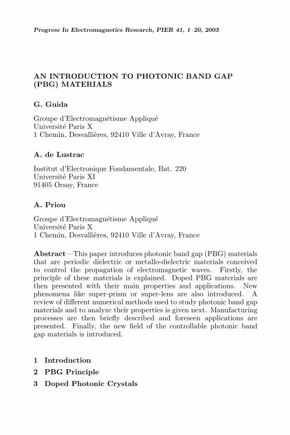
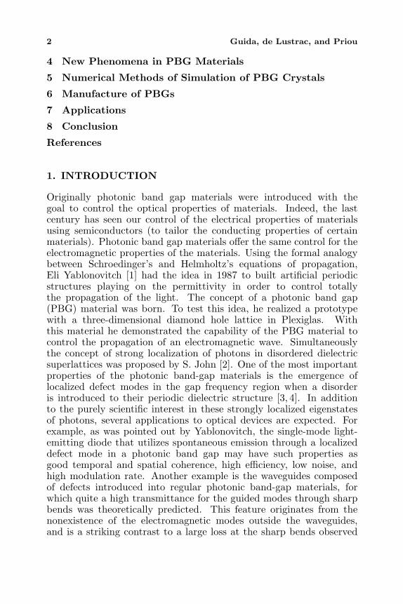
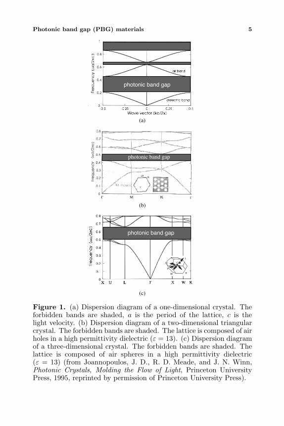
PBG materials have a periodic arrangement of the permittivity. Byanalogy with semiconductor physics where a crystal lattice corre-sponds to a periodic arrangement of the atomic potential [27], PBGmaterials are also called photonic crystals (PC). The periodicity ofthe permittivity plays the same role for the photons that propagateinside the structure than the atomic potential for the electrons.Leading further this analogy, the geometry and the index contrastof the photonic crystal determinate many of its optical propertiesas it does for conduction properties of semiconductors. Playing onthese two parameters, we can obtain frequency ranges for which lightpropagation is forbidden in the material and others ranges for whichlight can propagate. These frequency ranges are also scale dependent.Reducing the size of the elementary cell of the periodic lattice shiftsthe whole frequency range to higher values. The consequence of thisproperty is the possibility to transpose a photonic crystal design fromthe microwave domain to infrared or visible range. For example aPBG material for the 1–5 GHz frequency domain will have a typicalelementary cell size of a few centimeters and is very simple to realizeexperimentally. The same photonic crystal, designed to operate in theinfrared domain has a cell size of about 1µm and 0.1µm to operatein the visible domain. This frequency range is usually calculatedeither by using an analogy with the band structure for which theY -axis, representing the energy data, is swapped for the frequencyor by calculating the spectrum that is the reflection coefficient of afinite layer of photonic crystal. Figure 1 shows band structures fora one-dimensional, a two-dimensional and a three-dimensional PBGmaterials respectively. The forbidden bands are shaded on this figure.The first function of a 3D PBG material is then a lossless isotropicmirror for one or several frequency ranges. A 2D PBG material behavesas a mirror only in two directions as revealed by Figure 2 and a onedimensional material has only one favored wave propagation direction.The same material is theoretically transparent for the complementaryfrequency bands.
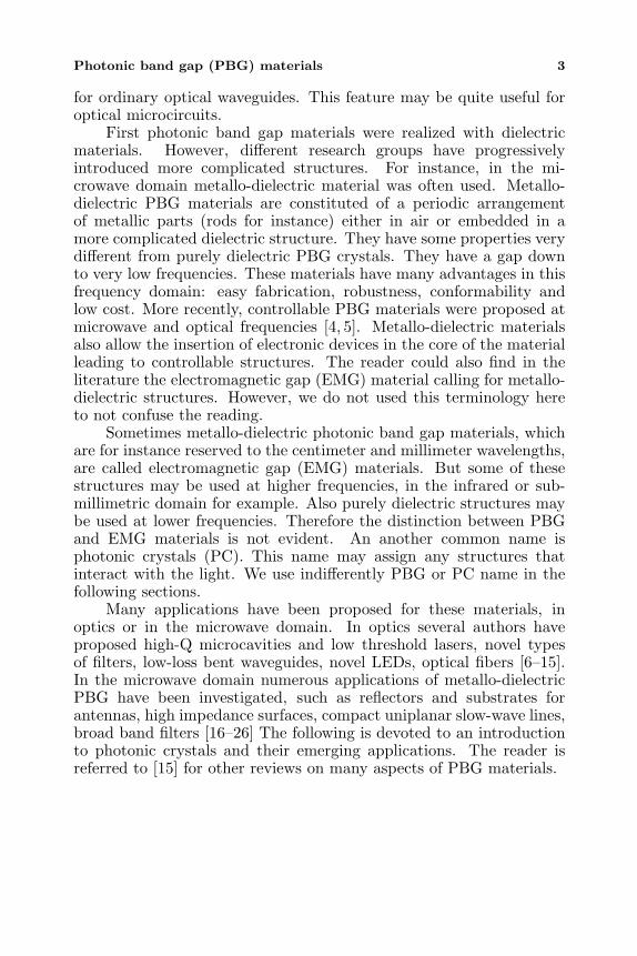
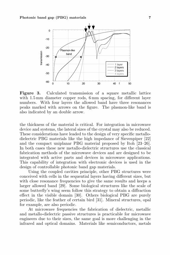
In the microwave domain, metallic lattices have very interestingproperties like, for example, a forbidden band from zero frequencyto a frequency fp called plasmon-like frequency (Fig. 3) [28]. Thisfrequency corresponds to the largest wavelength of the field that fitsthe metallic grid. An allowed band follows this first forbidden band.The coupling of resonances of the different cavities of the crystal formsthis band. Then the width of the band is linked to the number ofthe cavities and to the strength of their coupling. The number of
Photonic band gap (PBG) materials 5
photonic band gap
(a)
photonic band gap
(b)
L
KW
X
U Γ
photonic band gap
(c)
Figure 1. (a) Dispersion diagram of a one-dimensional crystal. Theforbidden bands are shaded, a is the period of the lattice, c is thelight velocity. (b) Dispersion diagram of a two-dimensional triangularcrystal. The forbidden bands are shaded. The lattice is composed of airholes in a high permittivity dielectric (ε = 13). (c) Dispersion diagramof a three-dimensional crystal. The forbidden bands are shaded. Thelattice is composed of air spheres in a high permittivity dielectric(ε = 13) (from Joannopoulos, J. D., R. D. Meade, and J. N. Winn,Photonic Crystals, Molding the Flow of Light, Princeton UniversityPress, 1995, reprinted by permission of Princeton University Press).
6 Guida, de Lustrac, and Priou
-50
-40
-30
-20
-10
0
10 15 20 25 30 35 40 45 50
mesuresimulation
Tra
nsm
issi
on
(d
B)
Fr quence (GHz)Frequency (GHz)
measure
forbiddenbandallowed
bandallowed
band
(a)
(b)
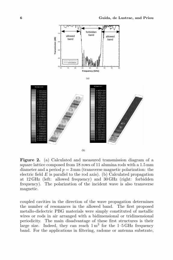
Figure 2. (a) Calculated and measured transmission diagram of asquare lattice composed from 18 rows of 11 alumina rods with a 1.5 mmdiameter and a period p = 3 mm (transverse magnetic polarization: theelectric field E is parallel to the rod axis). (b) Calculated propagationat 12 GHz (left: allowed frequency) and 30 GHz (right: forbiddenfrequency). The polarization of the incident wave is also transversemagnetic.
coupled cavities in the direction of the wave propagation determinesthe number of resonances in the allowed band. The first proposedmetallo-dielectric PBG materials were simply constituted of metallicwires or rods in air arranged with a bidimensional or tridimensionalperiodicity. The main disadvantage of these first structures is theirlarge size. Indeed, they can reach 1 m3 for the 1–5 GHz frequencyband. For the applications in filtering, radome or antenna substrate,
Photonic band gap (PBG) materials 7
-60
-50
-40
-30
-20
-10
0
0 10 20 30 40 50
1 layer2 layers3 layers4 layers
trans
mis
sion
f
Plasmon-likeband
Figure 3. Calculated transmission of a square metallic latticewith 1.5 mm diameter copper rods, 6 mm spacing, for different layernumbers. With four layers the allowed band have three resonancespeaks marked with arrows on the figure. The plasmon-like band isalso indicated by an double arrow.
the thickness of the material is critical. For integration in microwavedevice and systems, the lateral sizes of the crystal may also be reduced.These considerations have leaded to the design of very specific metallo-dielectric PBG materials like the high impedance of Sievenpiper [22]and the compact uniplanar PBG material proposed by Itoh [23–26].In both cases these new metallo-dielectric structures use the classicalfabrication methods of the microwave devices and are designed to beintegrated with active parts and devices in microwave applications.This capability of integration with electronic devices is used in thedesign of controllable photonic band gap materials.
Using the coupled cavities principle, other PBG structures wereconceived with cells in the sequential layers having different sizes, butwith close resonance frequencies to give the same results and keeps alarger allowed band [29]. Some biological structures like the scale ofsome butterfly’s wing seem follow this strategy to obtain a diffractioneffect in the visible domain [30]. Others biological PBG are purelyperiodic, like the feather of certain bird [31]. Mineral structures, opalfor example, are also periodic.
At microwave frequencies the fabrication of dielectric, metallicand metallo-dielectric passive structures is practicable for microwaveengineers due to their sizes, the same goal is more challenging in theinfrared and optical domains. Materials like semiconductors, metals
8 Guida, de Lustrac, and Priou
or composite were used [32]. As the dimensions of these structures aremicrometric or nanometric in the infrared and optical domains, theyoften reach the limits of the microelectronic technology [33]. Actually,similar periodic structures like Frequency Selective Surfaces (FSS) werestudied many years ago [34]. The main differences between FSS andPBG materials are the third dimension used in the latter, the solidstate theory formulation of photonic crystals, and the highly attractiveconcept of defect in PBG.
3. DOPED PHOTONIC CRYSTALS
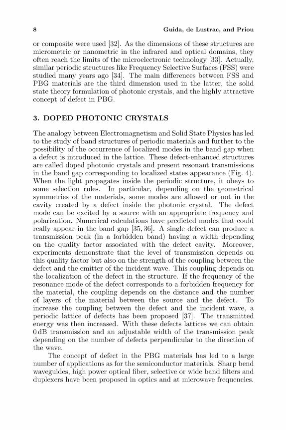
The analogy between Electromagnetism and Solid State Physics has ledto the study of band structures of periodic materials and further to thepossibility of the occurrence of localized modes in the band gap whena defect is introduced in the lattice. These defect-enhanced structuresare called doped photonic crystals and present resonant transmissionsin the band gap corresponding to localized states appearance (Fig. 4).When the light propagates inside the periodic structure, it obeys tosome selection rules. In particular, depending on the geometricalsymmetries of the materials, some modes are allowed or not in thecavity created by a defect inside the photonic crystal. The defectmode can be excited by a source with an appropriate frequency andpolarization. Numerical calculations have predicted modes that couldreally appear in the band gap [35, 36]. A single defect can produce atransmission peak (in a forbidden band) having a width dependingon the quality factor associated with the defect cavity. Moreover,experiments demonstrate that the level of transmission depends onthis quality factor but also on the strength of the coupling between thedefect and the emitter of the incident wave. This coupling depends onthe localization of the defect in the structure. If the frequency of theresonance mode of the defect corresponds to a forbidden frequency forthe material, the coupling depends on the distance and the numberof layers of the material between the source and the defect. Toincrease the coupling between the defect and the incident wave, aperiodic lattice of defects has been proposed [37]. The transmittedenergy was then increased. With these defects lattices we can obtain0 dB transmission and an adjustable width of the transmission peakdepending on the number of defects perpendicular to the direction ofthe wave.
The concept of defect in the PBG materials has led to a largenumber of applications as for the semiconductor materials. Sharp bendwaveguides, high power optical fiber, selective or wide band filters andduplexers have been proposed in optics and at microwave frequencies.
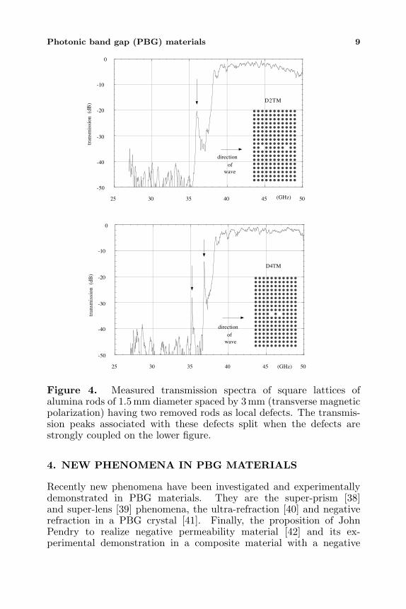
Photonic band gap (PBG) materials 9
-50
-40
-30
-20
-10
0
25 30 35 40 45 50
D2TM
tran
smis
sion
(dB
)
(GHz)
direction
of wave
-50
-40
-30
-20
-10
0
25 30 35 40 45 50
D4TM
tran
smis
sion
(dB
)
(GHz)
direction
of wave
Figure 4. Measured transmission spectra of square lattices ofalumina rods of 1.5 mm diameter spaced by 3 mm (transverse magneticpolarization) having two removed rods as local defects. The transmis-sion peaks associated with these defects split when the defects arestrongly coupled on the lower figure.
4. NEW PHENOMENA IN PBG MATERIALS
Recently new phenomena have been investigated and experimentallydemonstrated in PBG materials. They are the super-prism [38]and super-lens [39] phenomena, the ultra-refraction [40] and negativerefraction in a PBG crystal [41]. Finally, the proposition of JohnPendry to realize negative permeability material [42] and its ex-perimental demonstration in a composite material with a negative
10 Guida, de Lustrac, and Priou
permittivity part were a stimulating moment of the physics [43]. In thismaterial, a lattice of metallic stripes on a dielectric substrate realizesthe negative permittivity at frequencies corresponding to a forbiddenband. This material is called left-hand as the electric and magneticfields and the wave vector form a left-hand set. The capability tofabricate a material with simultaneously a negative permittivity andpermeability triggered many new fascinating applications for thesematerials. In the past, materials with an analog but disorderedstructure and totally different properties have been studied. They arecalled chiral materials [44]. In fact, they have disordered structuresand they have not shown negative permeability. Even if some of thesephenomena are linked, they show that the physics of the PBG crystalsis unexplored so far. Rigorous physical theory and numerical methodsof simulation allow this exploration.
5. NUMERICAL METHODS OF SIMULATION OF PBGCRYSTALS
There are six main methods to study numerically photonic crystals: (1)the Plane Wave Method [45], (2) the Finite Difference Time Domain(FDTD) method [46], (3) the Finite Element method [47], (4) the so-called Transfer Matrix Method (TMM) [48], (5) a method based on arigorous theory of scattering by a set of rods (for a two-dimensionalcrystal) [49] or a set of spheres (for a three-dimensional crystal) [50],and (6) the study of diffraction gratings [51]. All of these methodsare very efficient and revealed results highly accurate when comparedto experimental results. However depending on the problem tackled,they are not equivalent. Indeed, some of these methods like methods(1) to (4) have a high flexibility: they can simulate any doped or non-doped crystals [45–48]. Methods like method (5) are limited to certaintypes of PBG materials that are parallel cylinders (for 2d photoniccrystals) and spheres (for 3d) [49, 50]. Some of these methods likemethods (1), (4) and (6) can deal only with infinite crystals [45, 48, 51]and method (5) only with finite-sized structures [49, 50]. Finally, tostudy defect structures, methods (1), (4) and (6) use a super-cell. Onthe contrary, methods (2), (3) and (5) can deal with a finite structurehaving a single defect. In the following sections, we outline briefly thesemain numerical methods used to study doped and non-doped photoniccrystal properties.
The main advantage of the Plane Wave Expansion method isthat is very easy to implement and to obtain the band structure,since you specify the direction, and the codes give you all thepropagating/evanescent energies for that direction. A defect in the
Photonic band gap (PBG) materials 11
infinite photonic crystal will be treated using a super-cell. Theinterested reader can find in [45] information on the theory. Manyresults have been obtained with this method [52–56]. The limitationof the method is linked to the memory storage that depends on thenumber of plane waves used for the expansion of the field, and thisnumber escalates when the photonic crystal diverges from a periodicstructure. Sophisticated defects are then not possible.
The FDTD method analyses the Maxwell equations in timedomain. Many works on photonic crystals have been done using thismethod. Some works comparing FDTD results with experimentalmeasurements can be found in [57–63]. As for the Finite Elementmethod, electromagnetic modes of a defect can be calculated asthe transmission ratio of the material. To obtain the transmissionspectrum of the crystal, an electromagnetic pulse is send on thematerial and the output signal recorded. A fast Fourier transform isapplied to both incident and transmitted signals and the transmissionspectrum calculated. The FDTD method allows the simulation of finiteor infinite crystals with inner or outer electromagnetic sources. In somecases, this method permits the simulation of an entire experimental set-up with a PBG crystal. Results of this experiment are then analyzed.The FDTD method is the most commonly technique to simulate a PBGcrystal. The only limits of this method are the size of the memory tocalculate a large crystal and the lack of an accurate electromagneticmodel for some particular objects like thin wires for example. Anotheradvantage of this method is the attractive capability to simulate non-linear materials [46, 61].
The Finite Element method, well established in electromagnetism,has the great advantage to be implemented in very efficient commercialsoftware: MAFIA, HFSS, etc. This method can simulate infinite andfinite doped or non-doped crystals with inner or outer source [43].
The Transfer Matrix Method (TMM) is well described in [48].The method consists on writing the Maxwell’s equations in the k-space and rewriting them on a mesh. This is essentially a layer-by-layer calculation. The TMM is capable of handling PBG materialsof finite thickness. Structures with defects can be dealt only byconsidering a super-cell. An implementation of this method can befound on Internet [64]. The method permits to obtain band structuresand provides the reflectivity and transmission coefficients. Manyworks have used this method [65–69]. It has also proved particularlyuseful, and accurate, when comparisons with experimental structuresare undertaken [67, 69]. Recently, a new version of this method hasbeen developed to describe the emission properties of infinitely longcavity structures sandwiched between two photonic crystals [70]. The
12 Guida, de Lustrac, and Priou
limitations of the TMM method are the memory storage but also,although sophisticated versions of the method, it is difficult to dealwith a geometry different from the cubic geometry.
Many groups have implemented numerical methods based on therigorous scattering of light by a set of cylinders/spheres [49, 50]. Thetheory is very well explained in [49]. The photonic crystals are finite-sized. The main advantage of this method is that cylinders/spheres canbe located anywhere in space. Accordingly, a periodic arrangement isjust a particular case and it is possible to deal with a single defectwithout the need of a super-cell. In the same manner, it is very simpleto change the geometry of the structure. Although limitations arelinked to the size of the memory, a large number of cylinders has beenimplemented (about one hundred). As the dimension increases, thenumber of spheres must be smaller.
The use of diffraction gratings theory [51] allows the calculation ofreflection and transmission coefficients of a PBG structure constitutedof a stack of a finite number of infinite grating layers. The method candeal only with an infinitely long cavity as a defect for the structure.Moreover, to the best of our knowledge, this method can not simulatenew PBG materials that are sophisticated doped and active structures.
Others methods of simulation are less often used: the oscillatingdipole method [71–73], the real space green function method [74], theeigenmode expansion method [75], and the array scanning method [76].
6. MANUFACTURE OF PBGS
Several problems arise in manufacturing these structures. Of course,the difficulties encountered depend on the frequency domain wished.For the microwave domain, the typical size of the elementary cellconstituting the PBG material is of the order of the centimeter ormillimeter, and therefore can not generate any problem, generallyspeaking. For the optical domain, difficulties are highly significant.It is then necessary to evaluate tolerances of such materials [77–79].The next section is devoted to a brief description of a few techniquesused to build photonic crystals in the optical domain.
Many processes have been used to build photonic crystals. Themost common successful processes are based on classic microelectronicfabrication. One of these techniques is the electron beam lithographyand dry etching which provide three dimensions photonic crystalsworking in the optical domain [80]. In addition the layer-by-layerfabrication of diamond-like structure was successfully achieved in highrefractive index semiconductors by using the wafer fusion technique inIII-V [81]. Recently, Kawakami had the idea to fabricate 3D periodic
Photonic band gap (PBG) materials 13
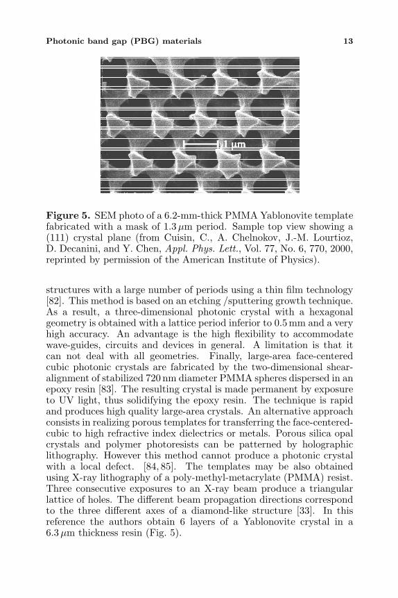
Figure 5. SEM photo of a 6.2-mm-thick PMMA Yablonovite templatefabricated with a mask of 1.3µm period. Sample top view showing a(111) crystal plane (from Cuisin, C., A. Chelnokov, J.-M. Lourtioz,D. Decanini, and Y. Chen, Appl. Phys. Lett., Vol. 77, No. 6, 770, 2000,reprinted by permission of the American Institute of Physics).
structures with a large number of periods using a thin film technology[82]. This method is based on an etching /sputtering growth technique.As a result, a three-dimensional photonic crystal with a hexagonalgeometry is obtained with a lattice period inferior to 0.5 mm and a veryhigh accuracy. An advantage is the high flexibility to accommodatewave-guides, circuits and devices in general. A limitation is that itcan not deal with all geometries. Finally, large-area face-centeredcubic photonic crystals are fabricated by the two-dimensional shear-alignment of stabilized 720 nm diameter PMMA spheres dispersed in anepoxy resin [83]. The resulting crystal is made permanent by exposureto UV light, thus solidifying the epoxy resin. The technique is rapidand produces high quality large-area crystals. An alternative approachconsists in realizing porous templates for transferring the face-centered-cubic to high refractive index dielectrics or metals. Porous silica opalcrystals and polymer photoresists can be patterned by holographiclithography. However this method cannot produce a photonic crystalwith a local defect. [84, 85]. The templates may be also obtainedusing X-ray lithography of a poly-methyl-metacrylate (PMMA) resist.Three consecutive exposures to an X-ray beam produce a triangularlattice of holes. The different beam propagation directions correspondto the three different axes of a diamond-like structure [33]. In thisreference the authors obtain 6 layers of a Yablonovite crystal in a6.3µm thickness resin (Fig. 5).
14 Guida, de Lustrac, and Priou
7. APPLICATIONS
The following section will address the foreseen applications of thePBG materials. If in the optical domain these applications arestill limited, they are already in practical development in microwavedomain. In optical domain we could then consider new highly efficientopto-electronic devices such as very efficient laser diodes [86], micro-scale light circuits [58], multiplexers or demultiplexers [39] based oninhibition of spontaneous emission [87], photoluminescence [56–57, 74],wave-guiding, super-prism phenomenon [38, 39]. Studies of plasmonfrequencies occurring for metal photonic crystals have also been ledshowing that the plasmon frequency can be controlled and could appearin the microwave region [28].
In the microwave domain the first applications appear. Manydevelopments concern the direct control of the electromagnetic energyand its transmission: mirrors, electromagnetic windows, active ra-domes, radiation pattern control [87–90]. We find also the highimpedance material of Sievenpiper [22] and the compact uniplanarPBG material proposed by Itoh [23–26]. Sievenpiper has proposedhis structure as perfect magnetic wall to reduce the leaky waves inantenna array. The material developed by Itoh and co-workers allowsthe realization of magnetic wall for waveguides, low loss coplanar linesand compact integrated filter. Others applications include duplexers[91] and controllable PBG materials. Due to a certain easiness offabrication in this frequency domain, the challenge of the electronicallycontrolled photonic crystals has a significant interest. Recent workshave demonstrated the capability to fabricate and to experimentallytest these materials [5]. Industrial applications of these crystalsare under development and concern mainly aerospace and telecomdomains.
8. CONCLUSION
The principle of PBG materials and their very peculiar properties havebeen described in this paper. The properties of doped crystals arevery similar to their semiconductor analogues. We have also reviewedthe main numerical methods used to study PBG materials. All thesemethods are attractive and have proved their efficiency by comparisonwith experiments or others numerical calculations. Alternatively,despite significant progresses, it is still a real challenge to build a perfectphotonic crystal in the optical domain. At microwave wavelength, thefabrication is easier and allows the insertion of electronic devices inthe crystal. Analyzing the tolerances of such a material then becomes
Photonic band gap (PBG) materials 15
necessary from an industrial point of view. At microwave frequencies,future studies should focus on telecom applications of passive andcontrollable PBG materials for which band gap frequency ranges andresonant peaks can be electronically controlled, and then should triggervery large potential of applications. This concept of controllability maybe applied to doped crystal where only defects are active. Indeed, theentire structure of the crystal should be also controllable, including itsdielectric or metallic properties. At optical frequencies the goal seemsto be the fabrication of the crystal and the insertion of light sources(laser, quantum boxes, polymers) in this structure.
REFERENCES
1. Yablonovitch, E., Phys. Rev. Lett., Vol. 58, 2059, 1987.2. John, S., Phys. Rev. B, Vol. 58, No. 23, 2486–89, 1987.3. Joannopoulos, J. D., R. D. Meade, and J. N. Winn, Photonic
Crystals, Molding the Flow of Light, Princeton University Press,1995.
4. Yablonovitch, E., Phys. Rev. Lett., Vol. 67, No. 17, 2295–2300,1991.
5. de Lustrac, A., F. Gadot, S. Cabaret, J. M. Lourtioz, T. Brillat,A. Priou, and E. Akmansoy, Appl. Phys. Lett., Vol. 75, No. 11,1625–1627, 1999.
6. Leonard, S. W., J. P. Mondia, H. M. van Driel, O. Toader, S. John,K. Busch, A. Birner, U. Gosele, and V. Lehmann, Phys. Rev. B,Vol. 61, R2389, Jan. 2000.
7. Painter, O., et al., Science, Vol. 284, 1819–1821, 1999.8. Villeneuve, P. R., et al., Appl. Phys. Lett., Vol. 67, No. 2, 167–170,
1995.9. Labilloy, D., et al., Phys. Rev. Lett., Vol. 79, No. 21, 4147–4151,
1997.10. Meade, R. D., et al., J. of Appl. Phys., Vol. 75, No. 9, 4753–4755,
1994.11. Mekis, A., S. Fan, and J. D. Joannopoulos, Phys. Rev. B, Vol. 58,
No. 8, 4809–4817, 1998.12. Boroditsky, M., et al., 1999 IEEE LEOS Annual Meeting Confer-
ence Proceeding, LEOS’99, 238–239, 1999.13. Knight, J. C., T. A. Birks, P. S. J. Russell, and D. M. Atkin,
Optics Letters, Vol. 21, No. 19, 1547–1549, 1996.14. Bjarklev, A., et al., J. of Optics A, Vol. 2, No. 6, 584–588, 2000.15. See review articles in the special issue on Photonic Crystals of
16 Guida, de Lustrac, and Priou
the Journal of Optical Society of America B, Vol. 10, 1993; orin the Journal of Modern Optics, Vol. 41, 1994. See also articlesin Photonic Band Gap Materials, C. M. Soukoulis (Ed.), KluwerAcademic Publishers, 1996 and the special issue of 1999 of theJournal of Lightwave Technologies.
16. Temelkuran, B. and E. Ozbay, Appl. Phys. Lett., Vol. 74, 486,1999.
17. Brown, E. R., C. D. Parker, and E. Yablonovitch, J. Opt. Soc.Am. B, Vol. 10, 404, 1993.
18. Brown, E. R. and O. B. McMahon, Appl. Phys. Lett., Vol. 68,1300, 1996.
19. Sigalas, M. M., et al., Micro. Opt. Tech. Lett., Vol. 15, 153, 1997.20. Temelkuran, B., et al., J. Appl. Phys., Vol. 87, 603, 2000.21. Thevenot, M., C. Cheype, A. Reineix, and B. Jecko, IEEE Trans.
Microwave Theory Tech., Vol. 47, 2115, 1999.22. Sievenpiper, D., L. Zhang, R. Broas, N. Alexopolous, and
E. Yablonovitch, IEEE Transactions on Microwave Theory andTechniques, Vol. 47, 2059–2074, 1999.
23. Yang, F. R., Y. Qian, R. Coccioli, and T. Itoh, IEEE Microwaveand Guided Wave Lett., Vol. 8, 372–374, Nov. 1998.
24. Yang, F. R., K. P. Ma, Y. Qian, and T. Itoh, IEEE Trans.Microwave Theory Tech., Vol. 47, No. 8, 1509–1514, Aug. 1999.
25. Ma, K. P., K. Hirose, F. R. Yang, Y. Qian, and T. Itoh, ElectronicLett., Vol. 34, No. 21, 2041–2042, Oct. 1998.
26. Yang, F. R., K. P. Ma, Y. Qian, and T. Itoh, IEEE Trans.Microwave Theory and Tech., Vol. 47, No. 11, 2092–2098.
27. Kittel, C., Solid State Physics, Dunod Paris, 1958.28. Pendry, J. B., Journal of Phys. Cond. Matter, Vol. 8, 1085–1108,
1996.29. Gadot, F., T. Brillat, E. Akmansoy, and A. de Lustrac, Electronic
Letters, Vol. 36, No. 7, 640–641, 2000.30. Vukusic, P., J.-R. Sambles, C.-R. Lawrence, and R. J. Wootton,
Proc. R. Soc. Lond. B, Vol. 266, 1403–1411, 1999.31. Lourtioz, J. M. and D. Maystre, Pour la Science, 66–73, Sept.
2000.32. Gupta, S., G. Tuttle, M. Sigalas, and K.-M. Ho, Appl. Phys. Lett.,
Vol. 71, No. 17, 2412, 1997.33. Cuisin, C., A. Chelnokov, J.-M. Lourtioz, D. Decanini, and
Y. Chen, Appl. Phys. Lett., Vol. 77, No. 6, 770–772, August 2000.34. Langley, T. K, R. J. Langley, and E. A. Parker, IEE Proc.-Microw.
Photonic band gap (PBG) materials 17
Antennas Propag., Vol. 143, No. 1, 62–66, 1996.35. Tayeb, G. and D. Maystre, Journal of Optical Society of America
A, Vol. 14, No. 12, 3323–3332, 1997.36. Villeneuve, P. R., S. Fan, and J. D. Joannopoulos, Phys. Rev. B,
Vol. 54, 7837–7842, 1996.37. Gadot, F., E. Akmansoy, A. de Lustrac, T. Brillat, A. Ammouche,
and J. M. Lourtioz, J. Appl. Phys., Vol. 85, No. 12, 8499–8501,1999.
38. Kosaka, H., T. Kwashima, A. Tomita, M. Notomi, T. Tamamura,T. Sato, and S. Kawakami, Physical Review B, Vol. 58, No. 16,10096–10099, 1998.
39. Kosaka, H., T. Kawashima, A. Tomita, M. Notomi, T. Tamamura,T. Sato, and S. Kawakami, Applied Physics Letters, Vol. 74,No. 10, 1370–1372, 1999.
40. Enoch, S., G. Tayeb, and D. Maystre, Optics Communications,Vol. 161, 171–176, 1999.
41. Gralak, B., S. Enoch, and G. Tayeb, Journal of Optical Society ofAmerica A, Vol. 17, No. 6, 1012–1020, 2000.
42. Pendry, J. B., A. J. Holden, D. J. Robbins, and W. J. Stewart,IEEE Trans. on Microwave Theory and Tech., Vol. 47, No. 11,2075–, 1999.
43. Smith, D. R., W. J. Padilla, D. C. Vier, S. C. Nemat-Nasser, andS. Schulz, Phys. Rev. Lett., Vol. 84, No. 18, 4184–4187, 2000.
44. See for example Chapter 10 devoted to the Microwave Propertiesof Chiral Composites, in Progress in Electromagnetics Research,A. Priou (Ed.), No. 6, Massachusetts, USA, 1992; or articlesrelated to chiral materials in Progress in Electromagnetics Re-search, A. Priou (Ed.), No. 9, Massachusetts, USA, 1994.
45. Pendry, J. B., J. Phys. Cond. Mat., Vol. 8, 1085–1108 andreferences therein, 1996.
46. Taflove, A., “Computational electrodynamics,” The Finite-Differ-ence Time-Domain Method, Artech House, Boston, London, 1995.
47. Pelosi, G., R. Coccioli, and S. Selleri (Eds.), Quick FiniteElements for Electromagnetic Waves, Arteh House.
48. Pendry, J. B. and A. MacKinnon, Phys. Rev. Lett., Vol. 69, 2772–2775, 1992.
49. Felbacq, D., G. Tayeb, and D. Maystre, Journal of the OpticalSociety of America A, Vol. 11, No. 9, 2526–2538, 1994.
50. de Daran, F., V. Vigneras-Lefebvre, and J. P. Parneix, IEEETrans. on Magnetics, Vol. 31, No. 3, 1598–1601, 1995.
18 Guida, de Lustrac, and Priou
51. Maystre, D., Pure Appl. Opt., Vol. 3, 975–993, 1994.52. See, for example, special issues on photonic crystals, J. Mod. Opt.,
Vol. 41, 1994; J. Opt. Soc. Am. B, Vol. 10, 1993.53. Meade, R. D., K. D. Brommer, A. M. Rappe, and
J. D. Joannopoulos, Phys. Rev. B, Vol. 44, 13772–13774, 1991.54. Smith, D. R., R. Dalichaouch, N. Kroll, S. Schultz, S. L. MacCall,
and P. M. Platzman, J. Opt. Soc. Am. B, Vol. 10, 314–321, 1993.55. Sakoda, K., Phys. Rev. B, Vol. 52, 8992–9002, 1995.56. Li, Z.-Y., L.-L. Lin, and Z.-Q. Zhang, Physical Review Letters,
Vol. 84, No. 19, 8, 4341–4344, 2000.57. Fan, S., P. R. Villeneuve, J. D. Joannopoulos, and E. F. Schubert,
Phys. Rev. Lett., Vol. 78, 3294–3297, 1997.58. Seo, Y.-S., K.-B. Chung, and H.-K. Hoeji, South Korea, Vol. 11,
No. 3, 198–201, 2000.59. Qiu, M. and S. He, J. of Appl. Phys., Vol. 87, No. 12, 8268–8272,
2000.60. Chan, C. T., Q. L. Yu, and K. M. Ho, Phys. Rev. B, Vol. 51,
16635, 1995.61. Ziolkowski, R. W. and M. Tanaka, J. Opt. Soc. Am, Vol. 16, No. 4,
930–940, 1999.62. Taflove (Ed.), Advances in Computational Electrodynamics, Ar-
tech House.63. Gadot, F., A. Ammouche, A. de Lustrac, A. Chelnokov,
F. Bouillault, P. Crozat, and J. M. Lourtioz, IEEE Trans. onMagn., Vol. 34, No. 5, Sept. 1998.
64. http://www.elec.gla.ac.uk/ areynolds/software.html.65. Sigalas, M. M., C. M. Soukoulis, C. T. Chan, and K. M. Ho, Phys.
Rev. B, Vol. 49, 11080–11087, 1994.66. Pendry, J. B. and L. Martin-Moreno, Phys. Rev. B, Vol. 50, 5062–
5073, 1994.67. Smith, D. R., S. Schultz, N. Kroll, M. Sigalas, K. M. Ho, and
C. M. Soukoulis, Appl. Phys. Lett., Vol. 65, 645–647, 1994.68. Ozbay, E., E. Michel, G. Tuttle, M. Sigalas, and K. M. Ho, Appl.
Phys. Lett., Vol. 65, 2059–2061, 1994.69. Gadot, F., A. Chelnokov, A. De Lustrac, P. Crozat, J. M. Lour-
tioz, D. Cassagne, and C. Jouanin, Appl. Phys. Lett., Vol. 71,1780–1782, 1997.
70. Guida, G., P. N. Stavrinou, G. Parry, and J. B. Pendry, to bepublished in the Journal of Modern Optics, 2000.
71. Sakoda, K. and H. Shiroma, Phys. Rev. B, Vol. 56, No. 8, 4830–
Photonic band gap (PBG) materials 19
4836, 1997.72. Kuzmiak, W. and A. Maradudin, Phys. Rev. B., Vol. 61, No. 16,
10750–10762, 2000.73. Maradudin, A. A. and A. R. McGurn, Photonic Band Gaps and
Localization, C. M. Soukoulis (Ed.), 247, Plenum Press, New York,1993.
74. McGurn, A. R., Phys. Rev. B, Vol. 53, No. 11, 7059–7065, 1996.75. Caloz, C., D. Curcio, A. Alvarez-Melcon, A. K. Skrivervik, and
F. E. Gardiol, Proceedings of the SPIE, The International Societyfor Optical Engineering, Vol. 3795, 176–187, 1999.
76. Caloz, C., A. K. Skrivervik, and F. E. Gardiol, Microwave andOptical Technology Letters, Vol. 24, No. 5, 316–322, March 5, 2000.
77. Lidorikis, E., M. M. Sigalas, E. N. Economou, and C. M. Souk-oulis, Phys. Rev. B, Vol. 61, No. 20, 13458–13464, 2000.
78. Li, Z.-Y., X. Zhang, and Z.-Q. Zhang, Phys. Rev. B, Vol. 63,No. 23, 15738–15747, 2000.
79. Guida, G., T. Brillat, A. Ammouche, F. Gadot, A. de Lustrac, andA. Priou, Journal of Applied Physics, Vol. 88, No. 8, 4491–4497,2000.
80. Forchel, A., M. Kamp, T. Happ, J. P. Reithmaier, M. Bayer,J. Koeth, and R. Dietrich, Microelectronic Engineering, Vol. 53,No. 1–4, 21–28, 2000.
81. Fleming, J. G. and S. Y. Lin, Opt. Lett., Vol. 24, No. 49, 1999.82. Kawakami, S., Electronics Letters, Vol. 33, No. 14, 1260–1261.83. Amos, R. M., T. J. Shepherd, J. G. Rarity, and P. Tapster,
Electronics Letters, Vol. 36, No. 16, 1411–1412, Aug. 3, 2000.84. Campbell, M., D. N. Sharp, M. T. Harrison, R. G. Denning, and
A. J. Tuberfield, Nature, Vol. 404, No. 53, London, 2000.85. Chelnokov, A., S. Rowson, J.-M. Lourtioz, V. Berger, and
J. Y. Courtois, J. Opt. A: Pure and Appl. Opt., Vol. 1, L3, 1999.86. Deppe, D. G., C. Lei, C. C. Lin, and D. L. Huffaker, Journal
of Modern Optics, Vol. 41, 325, 1994 and other articles onspontaneous emission on this volume of the JMO. (spontaneousand induced atomic decay, applications in the optical domain:laser diodes).
87. Zhu, S.-Y., Y. Yang, H. Chen, H. Zheng, and M. S. Zubairy,Physical Review Letters, Vol. 84, No. 10, 2136–2139, 2000.
88. Thevenot, M., A. Reineix, and B. Jecko, Microwave and OpticalTechnology Letters, Vol. 21, 411–414, 1999.
89. de Lustrac, A., T. Brillat, F. Gadot, and E. Akmansoy, to be
20 Guida, de Lustrac, and Priou
published in Applied Physics Letters.90. Temelkuran, B., M. Bayindir, E. Ozbay, R. Biswas, M. M. Sigalas,
G. Tuttle, and K. M. Ho, J. of Appl. Phys, Vol. 87, No. 1, 603–605,2000.
91. Ho, S. S., et al., Appl. Phys. Lett., Vol. 76, No. 16, 2301–2304,2000.


![Introducing Defects in Photonic Band-Gap (PBG) Crystals .../67531/metadc891074/m2/1/high_res_d/919424.pdf(AARD) at SLAC is a photonic band-gap (PBG) material with a hollow-core defect[1].](https://static.fdocuments.in/doc/165x107/5e65f48e19bce140d14229ec/introducing-defects-in-photonic-band-gap-pbg-crystals-67531metadc891074m21highresd919424pdf.jpg)
![Photonic Band Gap Computations [-2mm] - KITwieners/BandGapComputati… · Photonic Band Gap Computations Christian Wieners ... kS jkkkD 1 kS 0 j;k id Ad j;kR k: (this multigrid variant](https://static.fdocuments.in/doc/165x107/5a78add17f8b9a21538bcbf7/photonic-band-gap-computations-2mm-wienersbandgapcomputatiphotonic-band.jpg)

