Angstromology
60
Angstromology Introduction to Nanotechnology Foothill College
-
Upload
robert-cormia -
Category
Technology
-
view
1.139 -
download
0
Transcript of Angstromology

Angstromology
Introduction to NanotechnologyFoothill College

Overview
• Nanoscale definitions
• Scale and dimension (not just small)
• Working at the angstrom level– Nanotechnology – the last 200 years
• Nanotechnology – the next 100 years– Beyond nano – to pico scale and beyond
• Innovation in the quantum universe
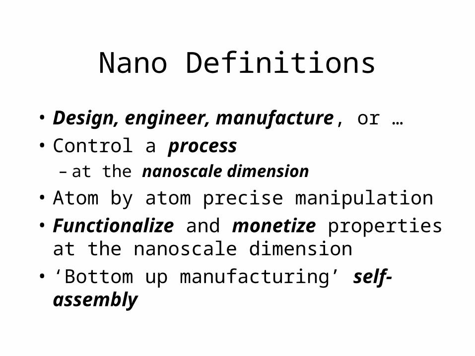
Nano Definitions
• Design, engineer, manufacture, or …
• Control a process– at the nanoscale dimension
• Atom by atom precise manipulation
• Functionalize and monetize properties at the nanoscale dimension
• ‘Bottom up manufacturing’ self-assembly

Traditional Nanotechnology

Nano Definitions Further
• Nanotechnology is the study, design, creation, synthesis, manipulation, and application of functional materials, devices, and systems through control of matter and energy at the nanometer scale (1–100 nanometers, one nanometer being equal to 1 × 10⁻⁹ of a meter).
• Exploitation of novel phenomena, including the properties of matter, energy, and information at the molecular, atomic, and sub atomic levels.

LEONARD MANDEL (at left) and co-workers at the University of Rochester gather around a parametric down-converter, an unusual crystal that converts any photon striking it into two photons with half as much energy. Mandel's group pioneered the use of the device in tests of quantum mechanics.
New experiments - real and imagined - are probing ever more deeply into the surreal quantum realm

Nanoscale Paradigm
Miniaturizationfrom thetop down
Moore’s Law 20th Century
Quantum propertiesfrom the bottom up
Moore’s Law 21st Century
Concept by Hilary Lackritz
1950 – 2000Era of materials
2000 – 2050Era of quanta

Scale and Dimension
• Quantum scale dimension– Small things– Short times– Small numbers– Low probabilities
• Heisenberg and Plank got it right– Heisenberg uncertainty principle
• Things happen differently at nanoscale

What could be nanotechnology?
• Chemistry
• Viral self-assembly
• Cellular process
• Nuclear fission
• Quantum computing
• Squeezed light
• Molecular tweezers

Chemistry
• Precision placement (yes)
• Molecule by molecule (maybe)
• Working with moles (a lot)
• Surface chemistry (always)
• Particles and colloids (if small enough)
• Chemists guide atoms and molecules to particular places (with help from nature)

Chemical Reaction
CO and O2 Reacting to Form CO2
Works in the gas phase but not on a surface!

Surface Femtochemistry
http://www.physik.fu-berlin.de/~femtoweb/newfemtos/surffemto/coox.php
COads + Oads ---- on transition metal surface ----> CO2 gas
Although the reaction cannot be initiated by conventional heating, excitation with a femtosecond pulse triggers the oxidation of CO on a ruthenium surface, leading to the formation of CO2.

Surface Femtochemistry
Sketch illustrating that only desorption occurs when the system is excited thermally, due to the lower energy required for CO-desorption than for O- activation. Under laser excitation, the 1.8 eV barrier for O-activation is overcome by coupling to the hot electrons, so that CO2 is formed.
http://www.physik.fu-berlin.de/~femtoweb/newfemtos/surffemto/coox.php

Potential energy surface for the CO/O/Ru(0001) system, constructed from spectroscopic data, assuming Morse potentials. Lines are the result of preliminary trajectory calculations. Going up, the O-CO distance increases, whereas the Ru-O distance remains constant: CO desorbs. To the right, the O-CO distance decreases (CO approaches oxygen), while O moves away from Ru: CO2 is formed and moves away from the surface. Thermally, only the pathway up is
accessible. Upon femtoseond excitation, regions of the potential energy surface become accessible that are inaccessible under thermal activation: The system is directed into new reactive regions.
Surface Femtochemistry
http://www.physik.fu-berlin.de/~femtoweb/newfemtos/surffemto/coox.php

Dendrimers
• Dendrimers– Branching– Stepwise growth– Globular nature– Functionalization
• Engineer like a protein– Surface energy / shape
• Can be grafted to C60 buckyballs / modified
• Controlling a processhttp://www.dendritech.com/


Cellular Processes
• DNA
• Micro RNAs
• Proteins
• Ribosomes
• Enzymes
• Lipid bilayer
• Ion channels
http://www.geosciences.unl.edu/~dbennett/
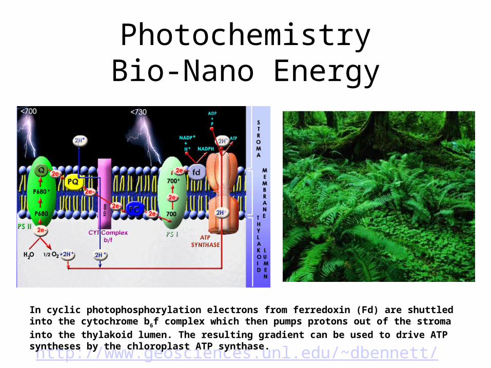
PhotochemistryBio-Nano Energy
In cyclic photophosphorylation electrons from ferredoxin (Fd) are shuttled into the cytochrome b6f complex which then pumps protons out of the stroma into the thylakoid lumen. The resulting
gradient can be used to drive ATP syntheses by the chloroplast ATP synthase.

Protein Capturing Light
http://www.cat.cc.md.us/~gkaiser/biotutorials/photosyn/photon.html
Photosynthesis moves EM energy into life through carbon

Protein Pumps and Energy
http://www.cat.cc.md.us/~gkaiser/biotutorials/photosyn/

Self Assembly
• Crystals
• Proteins
• Viruses
• Fractals
• Self-assembly is a process– Nature has harnessed it– Nanotechnology will harness it

Self Assembly
• Follows statistical thermodynamics
• Crystal growth follows symmetry rules
• Seen in molecular monolayers
• Building process for viral caspids
• Interaction of matter and information
• Use nature to guide manufacturing– Control and guide novel structures

Molecular Self Assembly
Figure1: 3D diagram of a lipid bilayer membrane - water molecules not represented for clarity
http://www.shu.ac.uk/schools/research/mri/model/micelles/micelles.htm
Figure 2: Different lipid model -top : multi-particles lipid molecule
-bottom: single-particle lipid molecule

Viral Self-Assembly
http://www.virology.net/Big_Virology/BVunassignplant.html

Bio-Nano Convergence
Jonathan Trent NASA - Ames

Nuclear Fission
• Fission at the pico scale
• Assembling a critical mass
• Creating a chain reaction– Controlling the number of events– Neutrons and the uranium U235 isotope
• Unleashes the power of a star– Required an understanding of the atom

Nuclear Fission

Thin Film Deposition
• Layer by layer deposition– Most thin film layers are 10 to 1000A thick– Deposition can occur one monolayer at a time
• Atom by atom nucleation– Clusters of atoms influence each other– Ordering process can occur very quickly
• Tailored properties based on process– Optical, electrical, and magnetic– Interfacial chemistry can be critical

Thin Film Deposition
http://www.fmf.uni-freiburg.de/projekte/pg_cluster/projekt_cluster/eci/eci_sim_e.html

Atomic Spectroscopy
• Energy and matter
• AES / LEEDS
• SEM / EDX
• ESCA / XPS
• XRF / EXAFS
• SIMMS

Photoelectric Effect
http://hypertextbook.com/physics/modern/photoelectric/

Quantum Computing
Three trapped 112Cd+ ions exhibit four different normal modes of oscillation in an asymmetric Paul trap
http://monroelab2.physics.lsa.umich.edu

Qubit Computing
• Qubit states• 00, 01, 10, 11• Qubit algorithms• New thinking• New problems
Centre for Quantum Computinghttp://www.qubit.org/

Uncertain Computing
• Quantum world is based in probabilities
• Quantum states can be either 1 or 0, or in some cases – both!
• Leverage uncertainty and ultra density for unimaginable speed:
• > 1022 transistors• > 1015 clock speed

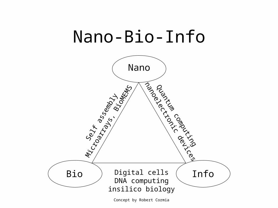
Nano-Bio-Info
Nano
Bio Info
Sel
f ass
embl
y
Mic
roar
rays
, Bio
ME
MS
Quantum
computing
nanoelectronic devices
Digital cellsDNA computinginsilico biology
Concept by Robert Cormia

Nano-Bio
• Using protein / viral complexes and DNA to self-assemble devices, and novel function, into biomechanical systems
Earth’s early nanostructures ~ 2 billion years ago

Digital Cells – Bio Informatics
http://www.ee.princeton.edu/people/Weiss.php
Modeling life as an information system

Nature as a Computer
• Biological systems like DNA and RNA especially appear to be more than networks of information.
• RNA itself can be seen as a molecular decision network

Nanoelectronics
• Pushing semiconductors to the edge
• Electrons moving too fast, or ‘confined’
• Band gap theory
• Quantum tunneling effects
• Semiconduction has always been ‘nano’– Now we are deliberately doing it

Nanoelectronics
Flux-qubit systems
Mesoscopic quantum systems SEM picture of a "persistent-current qubit" sample. The inner loop which contains three Josephson junctions is the qubit. The outer loop, containing two junctions, is a SQUID which measures the qubit's state. microwave pulses of variable length and amplitude to coherently manipulate the quantum state of the loop. The readout by the Squid was also pulsed and revealed quantum-state oscillations with high fidelity.
http://vortex.tn.tudelft.nl/research/fluxqubit/fluxqubit.html

Quantum Tunneling
• Breaking the quantum barrier– Quantum Tunneling in nanoelectronics– Macroscopic Quantum Coherence
• Meeting the particle / wave head on
• It can be a problem or a property– Clock speeds on the edge of tunneling– Or a way to store ‘information in energy’

Quantum Tunneling Transistor
http://www.aip.org/png/html/tunnel.htm http://www.sandia.gov/media/quantran.htm

Quantum Dots
• Quantum confinement– Energy and information states
• Small atomic assemblies
• Used in solar collection devices– With very high quantum efficiencies
• Applications in memory storage
• Applications in quantum computing

Quantum Dots
Quantum dots are small devices that contain a tiny droplet of free electrons. They are fabricated in semiconductor materials and have typical dimensions between nanometers to a few microns. The size and shape of these structures and therefore the number of electrons they contain, can be precisely controlled; a quantum dot can have anything from a single electron to a collection of several thousands. The physics of quantum dots shows many parallels with the behavior of naturally occurring quantum systems in atomic and nuclear physics. As in an atom, the energy levels in a quantum dot become quantized due to the confinement of electrons. Unlike atoms however, quantum dots can be easily connected to electrodes and are therefore excellent tools to study atomic-like properties. There is a wealth of interesting phenomena that have been measured in quantum dot structures over the past decade.
http://qt.tn.tudelft.nl/research/qdots/

Carbon Nanotubes
• Like graphite but all coiled up
• Typically 10 Angstroms in diameter
• Two key parameters control properties– M/N ratio determines electrical conductivity
• SWNT and MWNT– Transistors, heat sinks, hydrogen storage
• Carbon fibers have come a long way!

Carbon Nanotube Structures

Nanotubes / Nanohorns
The electrical properties of nanotubes / nanohorns can change, depending on their molecular structure. The "armchair" type has the characteristics of a metal; the "zigzag" type has properties that change depending on the tube diameter—a third have the characteristics of a metal and the rest those of a semiconductor; the "spiral" type has the characteristics of a semiconductor.

Nanotube Properties
http://nanotech-now.com/nanotube-buckyball-sites.htm

Self Assembled Nanostructures?

Nanoscale Emergence
• We live in an ‘emergent’ universe– Billiard balls vs. fuzzy functions– Quantum rules have ‘leveled out’
• Ensembles act in Newtonian physics• In smaller networks of 1,000s of atoms
– Atoms influenced by the quantum world
• The trick is to tap the inner rules of nature, and design them into our world
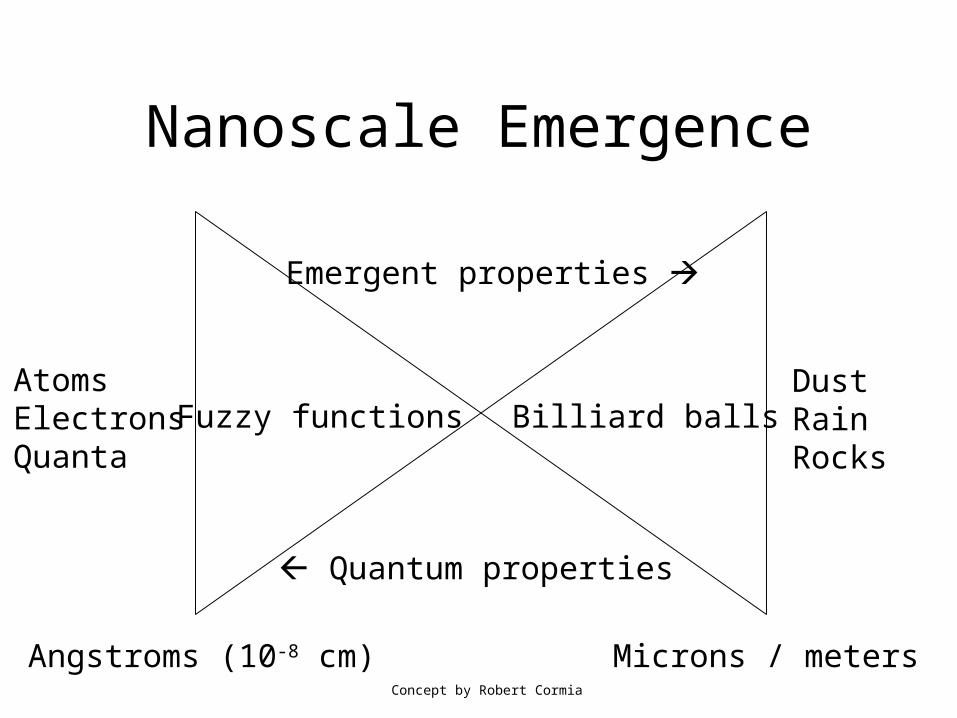
Nanoscale Emergence
Billiard ballsFuzzy functions
Angstroms (10-8 cm) Microns / meters
AtomsElectronsQuanta
DustRainRocks
Emergent properties
Quantum properties
Concept by Robert Cormia

What Really Defines ‘Nano’?
• Working at the ‘quantum scale’ – Working in small numbers– Working in small dimensions– Working in small time scales
• Let the universe drive – but we steer– Self assembly, quantum computing
• Trapping nano properties at the macro scale – tailoring key physical properties

Nanoscale Dimension - EMI
Mass
Energy Information
Forc
esS
elf-assembly
Quantum states
Concept by Robert Cormia

Nanoscale Dimension - EMI
• Matter• Energy• Information
• Forces• Quantum states• Self assembly
Force – interaction of matter and energyQuantum states – interaction of energy and informationSelf assembly – interaction of matter and information
Nanotechnology touches the ‘inner universe’

Nanoscale Engineering @ EMI
• Energy– Tunneling in quantum devices, band gaps
• Mass– Melting points, strength, self-assembly
• Information– Quantum computing / genetic algorithms
• Real nanotechnology occurs @ EMI

Summary
• Everything is small – big is an illusion• Small is necessary, but not sufficient
– Small just gets you to the quantum world
• Design, engineer, and / or manufacture– Or control a quantum mechanical process
• Functionalize and monetize at ‘small’– Nanoscience and nanotechnology @EMI
• Let the quantum universe help us out

Orders of Scale• Giga – billion, 10 e9• Mega – million, 10 e6• Kilo – thousand, 10 e3• Macro – referring to big or visible• Milli – 10 e-3
• Micro – referring to small, also 10 e-6
• Nano – 10 e-9
• Pico – 10 e-12
• Femto – 10 e-15