
F2-C: THz Imager and Science of Broadband Thz Wave Photonics
1st Annual Conference of COST Action MP1204
and
International Conference on Semiconductor Mid-IR
Materials and Optics SMMO2013
Book of abstracts
February 27th March 2nd, 2013

The authors acknowledge support from MPNS COST ACTIONMP1204 TERA-MIRRadiation: Materials, Generation, Detection and Applications
ii

Contents
Invited talks 1H. AltanDevelopment of a Rapid-Scan Fiber-Integrated Terahertz Spectrometer 2T.M. Benson Towards Mid-Infrared Sources Based on Chalcogenide Glass
Fibres . . . . . . . . . . . . . . . . . . . . . . . . . . . . . . . . . . . . . . 3T. Czyszanowski Single mode VCSEL arrays . . . . . . . . . . . . . . . . . . 4R. Morandotti Broadband Non-Reciprocal THz Isolator . . . . . . . . . . . . 6C. Sirtori Charged induced coherence for super-radiant optoelectronic device 8F. Tittel The state-of-the-art and grand challenges of Mid-IR technology and
applications . . . . . . . . . . . . . . . . . . . . . . . . . . . . . . . . . . . 9M.S. Vitiello Terahertz Photonics: from narrow-linewidth THz quantum cas-
cade lasers to nanowire and graphene THz photodetectors . . . . . . . . . 10
Contributed talks 11A. Andreone THz spatial light modulators based on hybrid metamaterials . . 12A. Bogris Modulation and noise properties of injection locked quantum cas-
cade lasers . . . . . . . . . . . . . . . . . . . . . . . . . . . . . . . . . . . . 13I. Buchvarov Multi-mJ, High Power, Mid-IR Tunable PPSLT OPO/OPA for
Ecient Tissue Ablation with Little Collateral Damage . . . . . . . . . . . 17M. Bugajski Mid-IR quantum cascade lasers at ITE . . . . . . . . . . . . . . 18M. Janek Chemical sensing of conned clay systems using THz-TDS . . . . . 19F. Janiak Optical properties of type II quantum wells based on GaSb emitting
in a mid infrared range . . . . . . . . . . . . . . . . . . . . . . . . . . . . . 20L. Juul An Impedance Matching Network for Centroid Fed Terahertz Antennas 21M. Klimczak Mid-infrared supercontinuum generation in soft-glass suspended
core photonic crystal be . . . . . . . . . . . . . . . . . . . . . . . . . . . . 23W. Knap Limits of Broadband THz Detectors Based on Plasma Oscillations
in Field Eect Transistors . . . . . . . . . . . . . . . . . . . . . . . . . . . 24A. Krotkus THz Time-Domain-Spectroscopy systems based on photoconduc-
tive components made from GaAsBi . . . . . . . . . . . . . . . . . . . . . . 25P. Martyniuk Modeling of InAsSb/AlAsSb nBn HOT detector's performance
limit . . . . . . . . . . . . . . . . . . . . . . . . . . . . . . . . . . . . . . . 26M. Motyka Fourier Transformed infrared modulation spectroscopy . . . . . . 28J. Muszalski Current state of the VECSEL development in ITE . . . . . . . . 29T.J. Ochalski Direct and indirect carbonation level estimation using MIR
sensing . . . . . . . . . . . . . . . . . . . . . . . . . . . . . . . . . . . . . . 30N. Palka Non-destructive evaluation of composite materials after dynamic
load in the terahertz range . . . . . . . . . . . . . . . . . . . . . . . . . . . 31M.F. Pereira Coupled polaritons and antipolaritons in dispersive gain media . 32
iii

M.F. Pereira THz intervalence antipolaritons . . . . . . . . . . . . . . . . . . 33P. Peterka Components for thulium-doped ber lasers . . . . . . . . . . . . . 34A. Piotrowski Uncooled mid and longwavelength infrared detectors . . . . . . 35. Piskorski Mid-infrared InP-based GaInNAs quantum-well VCSELs . . . . 36A. Portieri Overview of real-world Terahertz applications . . . . . . . . . . . 37M. Simonetta THz wave generation and detection using a single photomixer
antenna . . . . . . . . . . . . . . . . . . . . . . . . . . . . . . . . . . . . . 38A.K. Sokóª A numerical model of carrier transport in mid-IR VECSELs . . . 39J. Stiens Thin disk low voltage normal incidence single quantum well mid-
infrared modulator operating in retro-reection mode . . . . . . . . . . . . 40V. Spagnolo Mid infrared ber-coupled QCL-QEPAS sensor . . . . . . . . . . 41S. Wang Dilute bismides for infrared optoelectronics applications . . . . . . . 42D.O. Winge Modelling Gain under Operation in Quantum Cascade Lasers . . 43
Posters 44J. Cimek Characterization of microlenses made of tellurite and heavy metal
oxide glass developed with hot embossing technology . . . . . . . . . . . . 45G. Cywi«ski Optimization of Epitaxial Structures for Terahertz Emitters
Based on GaN/AlGaN HEMTs . . . . . . . . . . . . . . . . . . . . . . . . 47E. Czerwosz CNT-Pd-C nanocomposite lms for terahertz applications . . . 49K. CzubaNumerical calculations of SAGCM type InGaAs/InAlAs/InP avalanche
photodiode with monolithic refractive optics . . . . . . . . . . . . . . . . . 50M. Dyksik Infrared modulation spectroscopy for spin orbit interaction deter-
mination in semiconductors . . . . . . . . . . . . . . . . . . . . . . . . . . 51E. Machowska-Podsiadªo Predicting optical properties of InAs/GaSb super-
lattices in dierent temperatures . . . . . . . . . . . . . . . . . . . . . . . . 52A. Manolescu Electronic transport through a quantum nanosystem in a pho-
ton cavity . . . . . . . . . . . . . . . . . . . . . . . . . . . . . . . . . . . . 54M. Mernea Protein dynamics in solutions of dierent pH values probed by
THz spectroscopy and molecular modeling . . . . . . . . . . . . . . . . . . 55D.F. Mihailescu Alteration of protein structure and exibility by glycation
investigated by THz spectroscopy and molecular modeling . . . . . . . . . 56J. Mikoªajczyk Application of quantum cascade lasers to pollutant gases
detection . . . . . . . . . . . . . . . . . . . . . . . . . . . . . . . . . . . . . 57J. Mikoªajczyk High-current driver for quantum cascade lasers . . . . . . . . 58T.I. Milenov Recent Results on Synthesis and Characterization of Monoclinic
Ag2Te Crystals . . . . . . . . . . . . . . . . . . . . . . . . . . . . . . . . . 59M. Nowakowski Laboratory setup for laser absorption spectroscopy with
quantum cascade lasers . . . . . . . . . . . . . . . . . . . . . . . . . . . . . 60E. Pruszy«ska-Karbownik Analysis of mode hopping in a quantum cascade
laser through the study of far-eld . . . . . . . . . . . . . . . . . . . . . . . 61B. Siwicki Characterization of large core photonic crystal ber made of lead-
bismuth-galate oxide glass for broadband infrared transmission . . . . . . . 62M.P. Telenkov Dynamics of carrier distribution and population inversion in
Landau level system in resonant tunneling quantum well structures . . . . 63
Exhibitors 65AM Technologies . . . . . . . . . . . . . . . . . . . . . . . . . . . . . . . . . . . 66APVacuum . . . . . . . . . . . . . . . . . . . . . . . . . . . . . . . . . . . . . . 67
iv

EVG . . . . . . . . . . . . . . . . . . . . . . . . . . . . . . . . . . . . . . . . . . 68F&K Delvotec . . . . . . . . . . . . . . . . . . . . . . . . . . . . . . . . . . . . . 69Hirox . . . . . . . . . . . . . . . . . . . . . . . . . . . . . . . . . . . . . . . . . . 70Labsoft . . . . . . . . . . . . . . . . . . . . . . . . . . . . . . . . . . . . . . . . 71Olympus . . . . . . . . . . . . . . . . . . . . . . . . . . . . . . . . . . . . . . . . 72Uni - Export Instruments . . . . . . . . . . . . . . . . . . . . . . . . . . . . . . 73
v

vi

Invited talks
1
Development of a Rapid-Scan Fiber-Integrated Terahertz
Spectrometer
H. Altan1, H. Keskin1, S. Yavas2, F.Ö. lday2, K. Eken3, and A.B. Sahin4
1 Department of Physics, Middle East Technical University, Cankaya, 06800 Ankara,Turkey
2Department of Physics, Bilkent University, Cankaya, 06800 Ankara, Turkey3FiberLAST, ODTU Teknokent Galyum Blok Z-3, 06800 Ankara, Turkey
4Department of Electrical and Communication Engineering, Yldrm Beyazt University,Altnda§, 06050 Ankara, Turkey
Scientists in terahertz (THz) wave technologies have beneted from the recent de-velopments in ultrafast laser technologies and RF technologies and applied these newgained techniques into characterizing a wide variety of phenomena. Undoubtedly, themost successful of these applications has been in the development of time-domain tera-hertz spectroscopic and imaging systems which has been utilized in the characterizationof dielectrics and semiconductors. This pulsed technique has allowed users to characterizedynamical behavior inside materials under illumination with picosecond resolution. Typ-ically pump/probe or similar dynamical measurements require the use of amplied pulsesderived from free-space solid state lasers in the µJ-mJ range and since interferometrictechniques are typically used in pulsed measurements the measurement time of a THzspectrum can last at least tens of minutes. Better systems can be realized based on berlaser technologies. Here we discuss the adavantages of a THz spectrometer driven by anultrafast Ytterbium (Yb) doped ber laser whose repetition rate can be tuned rapidlyallowing for rapid dynamical measurements. The ecient gain medium, robust operationand compact design of the system opens up the possibility of exploring rapid detectionof various materials as well as studying dynamical behavior using the high brightnesssource. Work in this area will be discussed in the context of the current work done in ourrespective institutions, and future prospects for this technology.
2

Towards Mid-Infrared Sources Based on Chalcogenide
Glass Fibres
T.M. Benson1, . Sójka12, Z. Tang1, E. Bere±-Pawlik2, E.R. Barney1,D. Furniss1, A.B. Seddon1, and S. Sujecki1
1George Green Institute for Electromagnetics Research, University of Nottingham,University Park, NG7 2RD Nottingham, UK
2Institute of Telecommunication, Teleinformatics & Acoustics, Wrocªaw University ofTechnology, Wybrze»e Wyspianskiego 27, 50-370 Wrocªaw, Poland
Chalcogenide glass bres operating in the mid-infrared part of the electromagneticspectrum oer signicant opportunity in real-time sensing, imaging and power delivery.When doped with rare-earth ions these bres also have prospective as mid-IR integratedlasers because of their potentially low optical loss at expected pump and emission wave-lengths and low phonon energies. In this presentation we will describe our experimentaland modelling work on chalcogenide glasses and bres doped with Dy3+, Pr3+ or Tb3+
which targets laser operation at wavelengths of 4.6µm, 4.89µm and 7.5µm respectively.Some of the key factors that have emerged are shown to be host-glass composition and pu-rity, rare-earth solubility with an increase in the concentration of rare earth ion increasingclustering and the tendency for crystallisation to occur, and the ability to subsequentlydraw to bre. Nevertheless our simulations demonstrate that ecient mid-infrared laseraction is possible for all the dopants considered provided that optical losses (currentlyassumed wavelength-invariant) are kept at or below 1 dBm−1.
The large optical nonlinearity of chalcogenide glasses also makes them an attractiveoption for super-continuum generation (SCG). We will also briey consider SCG in chalco-genide glass bres as a means for achieving bright broadband sources for spectroscopy.
3

Single mode VCSEL arrays∗
T. Czyszanowski1, M. Dems1, M. Wasiak1, R.P. Sarzaªa1, E. Lamothe2,N. Volet2, V. Iakovlev2, and E. Kapon2
1Institute of Physics, ód¹ University of Technology, ul. Wólcza«ska 219, 90-924 ód¹,Poland
2Laboratory of Physics of Nanostructures, École Polytechnique Fédérale de Lausanne(EPFL), CH-1015 Lausanne, Switzerland
The ecient way to increase the emitted power by VCSEL is to combine severalemitters into phase-locked array. There is a strong motivation to develop a design of theVCSEL arrays that will emit in a single and narrow linewidth. In VCSEL arrays onecan observe two types of modes. First kind are modes of single emitters, second are thearray supermodes formed of the same order of single-emitter modes. The key to narrowthe width of emission spectrum is to reduce the number of existing modes down to onlyone. First kind of modes are known to be governed mainly by the dimension of the singleemitter and patterning of optical connement. The type and number of design parametersthat control the second kind of the modes is known much less.
In this paper we present the simulation results of optimization of carrier injection,heat ow and optical connement aimed for single mode operation. The analyzed struc-ture incorporates InAlGaAs quantum wells within InP cavity. The cavity is bounded byAlGaAs/GaAs DBRs. The tunnel junction is responsible for carrier funneling into theactive region. We investigate three type of optical connement:
Type1 no intentional optical pattern but thermal focusing
Type2 air-gaps etched at the interface between top DBR and cavity
Type3 anti-resonant reecting optical waveguide (ARROW) at the interface be-tween top DBR and cavity
To rigorously simulate the physical phenomena taking place in the device we usedmulti-physical model, which comprises in the selfconsistent manner three-dimensionalmodels of optical (Plane Wave Admittance Method), thermal, electrical and diusion(Finite Element Method) phenomena.
We perform the exhaustive modal analysis of the 1x3 VCSEL arrays. In the analysiswe investigate the inuence of the distance between emitters, their size and thickness ofthe optical patterning. The analysis is performed for broad range of injected currentsfrom threshold to the rollover. As the result we illustrate the complex competition ofthe modes, inuence of the optical connement on structure of the modes and determinethe geometrical parameters, which favor the array modes in the considered array designs.We show that rst two kinds of connement support multi-modal operation under largercurrents (Fig. 1a,b) and relatively low threshold, while third design provides control ofsingle mode operation for precisely designed ARROW structure (Fig. 1c) but suers fromlarger optical losses.
∗The project is supported by the Swiss National Science Foundation (SNF) through grant SCOPESIZ73ZO_128019 Coupled VCSEL arrays for gas-sensing and environmental control
4

a) b) c)
Figure 1: Modal gain of 1x3 VCSEL array of a) Type1 as a function of injected current,b) Type2 as a function of the etching depth of air-gap and c) Type3 as a function ofinjected current. The colors of the curves in a) represents the modes which form 1 lobein the single emitter (black), 2 lobes (green), 3 lobes (blue) and 4 lobes (red)
5

Broadband Non-Reciprocal THz Isolator
M. Shalaby1, M. Peccianti2, Y. Ozturk3, and R. Morandotti1
1INRS-EMT, Varennes, Quebec J3X 1S2, Canada2Institute for Complex Systems-CNR, Via dei Taurini 19, 00185 Rome, Italy
3Ege University, 35100 Izmir, Turkey
A Faraday isolator is an electromagnetic non-reciprocal device. It is required to shieldelectromagnetic sources against the detrimental eects of back-reected light. Althoughit was proposed by Rayleigh [1] and demonstrated in various spectral regimes, it has beenso far absent from the THz regime due to the limitations on handing the associated broadbandwidth. The THz isolator requires a broadband non-reciprocal phase retardation of45. This has always been extremely challenging to achieve over a wide bandwidth. Wehave recently demonstrated an isolator based on a magnetic non-reciprocal retarder op-erating with broadband THz pulses. Our device depends on permanently magnetizedStrontium Iron Oxide (SrFe12O19), where Faraday rotations up to (194/T) were ob-tained [2].
In comparison with previous studies on THz Faraday rotations [3], our sample hasthree main advantages that allowed for the realization of an isolator. First, it has a fer-romagnetic resonance in the sub-THz band ∼ 50 − 60 THz [4], i.e. the rotation is atin the THz region (above the resonance). Second, it belongs to the class of insulatingferromagnets. This means it shows similar magnetic properties to the conducting coun-terparts, its conductivity being reduced by many orders of magnitude. This leads to verylow absorption, which is a fundamental requirement for isolators. Third, it is a permanentmagnet, which allows for its use without the need for an external magnetic eld bias.
To build the isolator, we magnetized the sample to give a rotation of 45 upon singlepropagation, i.e. the reected pulse experienced a 90 rotation and got blocked by a0-aligned polarizer. Figure 1(a) shows a schematic diagram of the back-reection mea-surement setup that was used to characterize the isolator. The sample was placed betweentwo polarizers. As a typical isolator conguration, WGP4 ensured the horizontal polariza-tion of both the generated and the detected THz and WGP5 was aligned to 45. The THzreected o the mirror is detected in a ZnTe crystal by electro-optical sampling. Figure1(b) shows the phase retardation map where the back-reected THz is plotted for dier-ent levels of magnetic eld. Two cases are presented in Fig. 1(c), corresponding to thesample providing 0 and 45 rotations. As shown, in the case of an unmagnetized sample(0), the THz is reected back from a mirror towards the source. On the other hand, thelatter case demonstrates a fully functioning isolator where the back-reection is forbidden.The demonstrated isolator is just a specic case of a general THz non-reciprocal phaseretarder. Thanks to the large achievable retardations, by tuning the applied magneticeld, we managed to even reach phase reversal of the input eld as shown in the phaseretardation graph (Fig. 1(b)).
In conclusion, we demonstrated a fully functional THz isolator. Our device is capableof shielding back-reected THz in the range (0.08-0.8) THz. We believe that our resultwill pave the way to a new era of non-reciprocal THz devices, whether operating alone orcoupled to other reciprocal systems.
6
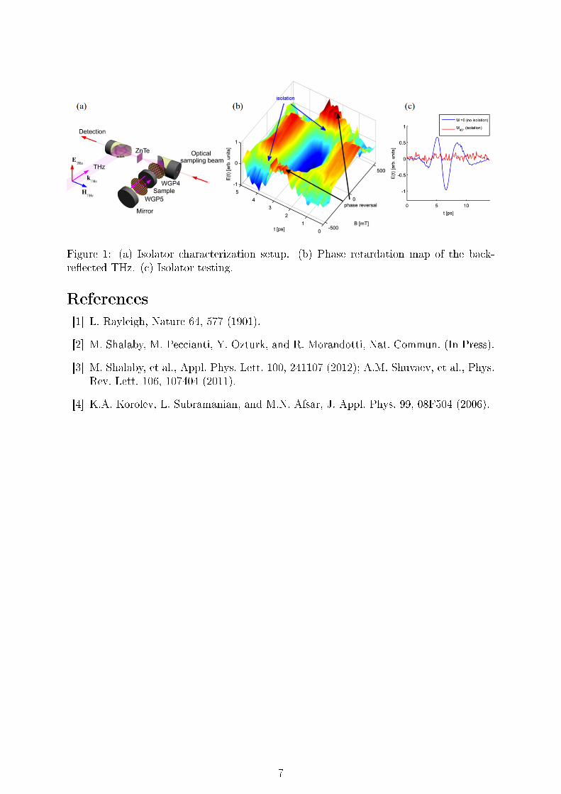
Figure 1: (a) Isolator characterization setup. (b) Phase retardation map of the back-reected THz. (c) Isolator testing.
References
[1] L. Rayleigh, Nature 64, 577 (1901).
[2] M. Shalaby, M. Peccianti, Y. Ozturk, and R. Morandotti, Nat. Commun. (In Press).
[3] M. Shalaby, et al., Appl. Phys. Lett. 100, 241107 (2012); A.M. Shuvaev, et al., Phys.Rev. Lett. 106, 107404 (2011).
[4] K.A. Korolev, L. Subramanian, and M.N. Afsar, J. Appl. Phys. 99, 08F504 (2006).
7

Charged induced coherence for super-radiant optoelec-
tronic device
C. Sirtori
Laboratoire Matériaux et Phénomènes Quantiques, Université Paris-Diderot, CNRSUMR7162, France
Light-matter strong interaction can be used to substantially modify the electronic spec-trum of semiconductor unipolar devices. In fact, electronic excitations, originating fromoptical transitions in quantum wells, can strongly interact with a microcavity photonicmode and give rise to mixed light-matter states, the polaritons. These new states are ener-getically separated from the original electronic states of the system and can be accessed byinjecting electrons into their matter part, thus obtaining ecient emitter and detectors inthe far- and mid-infrared wavelength range. To this end we have conceived new device ar-chitectures in which active materials are embedded within metal-dielectric micro-cavitieswith ultra-strong light connement in the order of Vµcavity/(λvaccum)3 = 10−6.
I will also show that to increase the coupling strength of the light matter interaction,thus separating even further the polaritonic states from those electronic, it is necessaryto increase the number of available dipoles that interact with the photons of the cavitymode. This is readily obtained by increasing the doping density. For very high electronicdensities, when the Fermi level occupies more than one subband, very important collectiveeects appear. The interaction between dipoles becomes so strong that phases all thetransitions of the systems giving rise to important renormalisation and supperradianteects.
We have measured a strong electroluminescent signal from these renormalized states,rst evidence of super-coherent emission.
References
[1] L. Sapienza, et al., Phys. Rev. Lett. 100, 136806 (2008)
[2] P. Jouy, et al., PRB 82, 045322 (2010)
[3] Y. Todorov, et al., Phys. Rev. Lett. 105, 196402 (2010)
[4] A. Delteil, et al., Phys. Rev. Lett. 109, 246808 (2012)
8
The state-of-the-art and grand challenges of Mid-IR tech-
nology and applications
F. Tittel
Rice Laser Science Group, Rice University, MS366, 6100 Main St., TX 77005 Houston,USA
This talk will focus on recent advances in the development of sensitive, selective, robustsensors based on mid-infrared semiconductor lasers for the detection of trace gas speciesand their applications in environmental monitoring, medicine and industrial process anal-ysis [1]. The architecture and performance of several trace gas sensors based on quantumand interband cascade lasers targeting strong fundamental rotational-vibrational transi-tions will be described. High detection sensitivity at ppbv and sub-ppbv concentrationlevels requires a sensitivity enhancement scheme such as an optical multipass gas cell,a cavity absorption enhancement technique, or photo-acoustic absorption spectroscopy.Several examples of autonomous, eld deployable gas sensors will be described.
References
[1] http://ece.rice.edu/lasersci/
9

Terahertz Photonics: from narrow-linewidth THz quan-
tum cascade lasers to nanowire and graphene THz pho-
todetectors
M.S. Vitiello12
1NEST, CNR Istituto Nanoscienze and Scuola Normale Superiore, Piazza SanSilvestro 12, 56127, Pisa, Italy
2CNR Istituto Nazionale di Ottica and LENS (European Laboratory for Non-linearSpectroscopy), Via Carrara 1, 50019 Sesto Fiorentino (FI), Italy
Recent results on the measurement of the intrinsic linewidth and on the analysis of thefrequency noise features of Terahertz Quantum Cascade Lasers (QCLs) will be discussed,together with their potential in polarization spectroscopy experiments addressed to highsensitivity molecular detection and their phase lock to a free space THz frequency comb.
A general overview on our novel approaches to Terahertz detection will be nally givenby demonstrating antenna-coupled eld eect transistors as plasma-wave THz detectorsin both InAs nanowire and graphene channel material. Room temperature operationin the 0.3 3 THz range is reported with noise equivalent powers as low as a few 10 11 W/Hz1/2, and high-speed response.
10

Contributed talks
11

THz spatial light modulators based on hybrid metama-
terials
N. Chikhi1, M. Lissitskii2, A. Andreone1
1University of Naples Federico II, Piazzale Tecchio 80, Naples, Italy2Institute of Cybernetics E. Caianiello, Comprensorio Olivetti, Pozzuoli (Na), Italy
Large frequency tunability is achieved by combining a planar metamaterial with liquidcrystal (LC) having a relatively high birefringence. The device is based on the exploitationof the LC molecule reorientation to change the permittivity of dierent capacitors presentin the unit cells based on Split Ring Resonators. The whole system is designed to obtaina maximum signal frequency shift up to 8% around the operational frequency of 1 THz.The possible application of this structure as a Spatial Light Modulator is discussed.
12

Modulation and noise properties of injection locked quan-
tum cascade lasers∗
H. Simos1,2, A. Bogris1,3, D. Syvridis1
1Department of Informatics and Telecommunications, National and KapodistrianUniversity of Athens, Panepistimiopolis, Ilissia, 15784, Athens, Greece
2Department of Electronics, Technological Educational Institute of Piraeus Egaleo,Greece
3 Department of Informatics, Technological educational institute of Athens, Egaleo,Greece
Quantum-cascade lasers (QCLs) are IR sources based on intersubband transitions thatcan operate in a wide range of wavelengths (from 3.5 to 150µm) [1]. Powerful emission canbe obtained from a single emitter in continuous wave (CW) mode at room temperature(RT) [1]. Although QCL technology is nowadays accepted as the dominant one for thesupport of transmission at the MIR range, it has not been possible to exhibit sub-shotnoise performance for these lasers till today.
The low noise performance in typical interband diode lasers has been demonstratedby either increasing the bias current so as to suppress the spontaneous emission noise.Alternatively, the researhers have achieved low intensity noise performance by utilizinginjection locking so as to approach the saturation regime with optical pumping insteadof using electrical pumping. The latter method seems more appropriate for QCL lasersfor which it is not easy to increase arbitrarily the electrical current as typical thresholdvalues are exceeding several hundreds of mA.
In this abstract we present the rst numerical results of a model which studies thenoise properties of injection locked lasers. Appart from this, using the same model weidentify regimes at which an injection locked laser can provide pure optical frequencymodulation which could be utilized in high sensitivity spectroscopy experiments.
The carrier and photon dynamics in the 3-level QCL approximation are describedby rate equations (RE) for the carrier number population for each level and the photonnumber. The RE system reads [2]
dN3
dt=ηI
q− N3
τ32− N3
τ31− g(N3 −N2)s+ F3 (1)
dN2
dt=N3
τ32− N2
τ21− g(N3 −N2)s+ F2 (2)
dN1
dt=N3
τ31− N2
τ21− N1
τout+ F1 (3)
dE
dt=
1
2
[Zg(N3 −N2)−
1
τph
](1− iα)E + Esp +
√κinj
τrEinj − iδωE(2) (4)
N3 = N3(t), N2 = N2(t), N1 = N1(t) are the carrier number at the correspondingenergy level, E = E(t) is the complex eld so that |E|2 = S (photon number). The phase
∗This work was supported by the European Communities Seventh Frame-work Programme FP7/2007-2013 under Grant 288304 (STREP CLARITY).
13

change is introduced through the linewidth enhancement factor (α). The spontaneousemission noise is introduced through Esp, which is a complex number:
Esp =
√1
2dtZ(gN3 + β
N3
τeS(x+ iy) (5)
where τe is the carrier lifetime and the numbers x and y are random Gaussian variableswith zero mean value and unit standard deviation. Details on the noise term derivationcan be found in [?].Moreover, g the gain coecient, β is the spontaneous emission factorand Z the number of stages. τph is the photon lifetime, τe is the carrier recombination timeand τij the transition characteristic times. I is the injection current and η is the injectioneciency. Finally, it is assumed that no other losses are present, thus all electrons escapingthe stage to the injector, reach the next stage.
The main parameters that aect the properties of the injection locked laser are thefrequency detuning between master and slave (δω) and the injection strength (kinj). Fig.1a shows the phase coherence between master and slave and Fig. 1b shows the relativeintensity noise of the free running laser and of the injection locked as well. 8 dB reductionof RIN noise is observed for the injection locked laser.
Figure 1: Left: Phase evolution of the master and the locked (slave) laser. Right: RINspectrum of the slave laser without locking (free running, black line) and the correspondingRIN spectrum after locking by the master laser (red line).
The dependence of the RIN values as a function of the frequency detuning betweenmaster and slave is depicted in g. 2. The gure shows that the QCL does not exhibita wide locking bandwidth (∼ 2 GHz) compared to typical interband lasers (for the sameinjection level the locking bandwidth exceeds 20 GHz).
The main reason for this dierence is probably the long cavity of approximately 2 mmfor the specic QCL under investigation which is ten times longer than that of typicalinterband lasers. Within the locking range, the RIN of the slave is substantially improved.
The intensity noise squeezing properties of injection locked lasers could be investigatedfrom the spectroscopy viewpoint. A nice example for investigation is the case where themaster laser is directly modulated at the current. This current modulation will result inboth amplitude and frequency modulation of the laser output. From the spectroscopicpoint of view, the frequency modulation is desired while the amplitude modulation is not.
14

Figure 2: Dependence of slave RIN performance as a function of the frequency detuningbetween master and slave. kinj = −10 dB.
Hence, an injection locked laser could provide low-noise, pure frequency modulation inthis case. Fig. 3 shows the power time traces for the master and the slave when theformer is directly modulated at 3 GHz (bias current 500 mA, modulation depth 20 mA,kinj = −15 dB). The time traces clearly show that slave has adequately suppressed theintensity modulation. Additionally slave is capable of following at a high degree thefrequency variations of the master's optical carrier hence providing the possibility forpure amplication of optical frequency modulation which is required for spectroscopyapplications.
Figure 3: Power time traces of master and slave outputs when the former is directlymodulated at 3 GHz.
15

Figure 4: Frequency modulation of the master and slave carriers due to master's currentmodulation.
References
[1] Federico Capasso, Optical Engineering 49 (11), 111102 (2010)
[2] T. Gensty,et al., Optics Communications, 256, pp 171-183, 2005.
16
Multi-mJ, High Power, Mid-IR Tunable PPSLT OPO/OPA
for Ecient Tissue Ablation with Little Collateral Dam-
age
D. Chuchumishev1, C-P Richter3,4, S. Philipov2, A. Gaydardzhiev1,I. Buchvarov1,3
1Department of Physics, Soa University, 5 James Bourchier Blvd., BG-1164 Soa,Bulgaria
2Department of Medicine, Soa University, 1 Kozyak Str., BG-1407 Soa, Bulgaria3Deptartment of Otolaryngology, Northwestern University, 303 E. Chicago Ave, Searle
12-561, Chicago, IL 60611, USA4Department of Biomedical Engineering, Northwestern University, 2145 Sheridan Road,
Tech E310, Evanston, IL 60208, USA
We demonstrate ecient tissue ablation using 5.7-mJ, mid-IR, PPSLT based OPO/OPApumped by 30-mJ 1.4 ns Nd-laser system, operated at 0.5-kHz repetition rate. The out-put wavelength is temperature tuned within the water absorption peak (3000-3500 nm).No tissue damages are found in a distance above 10 microns from the ablated surface.
17

Mid-IR quantum cascade lasers at ITE
M. Bugajski1, K. Kosiel1, P. Gutowski1, A. Szerling1, P. Karbownik1,A. Trajnerowicz1, K. Pier±ci«ski1, D. Pier±ci«ska1, J. Kubacka-Traczyk1,
I. Sankowska1, E. Pruszy«ska-Karbownik1, M. Sakowicz1,A. Wójcik-Jedli«ska1, G. Haªda±2, A. Kolek2
1Department of Photonics, Institute of Electron Technology, Warszawa2epartment of Electronics Fudamentals, Rzeszów University of Technology
In this paper we present the development of mid-infrared GaAs/AlGaAs QCLs tech-nology and discuss basic characteristics of lasers fabricated at the Institute of ElectronTechnology. We also show that reliable simulation methods which can deal with thecomplicated physical phenomena involved in the quantum cascade lasers operation arenecessary to predict the behaviour of new structures and optimize their performance.The developed lasers show the record pulse powers of 6 W at 77 K and up to 50 mW at300 K. This has been achieved by careful optimization of the epitaxial process and byapplying a high reectivity metallic coating to the back facet of the laser. The deviceshave been successfully used in prototype ammonia detection system working in ppb range.
18
Chemical sensing of conned clay systems using THz-
TDS∗
D. Zich1, J. Darmo2, T. Zacher1, V. Szöcs3, D. Lorenc4 and M. Janek1
1Comenius University, Faculty of Natural Sciences, Department of Physical andTheoretical Chemistry, Mlynská dolina CH1, SK-84215 Bratislava, Slovakia
2Institute of Phtonics, Vienna University of Technology, Guÿhausstraÿe 27-29, A-1040Vienna, Austria
3 Comenius University, Faculty of Natural Sciences, Institute of Chemistry, Mlynskádolina CH2, SK-84215 Bratislava, Slovakia
4 International Laser Center, Ilkovicova 3, SK-81219 Bratislava, Slovakia
Terahertz time-domain spectroscopy (THz-TDS) was used to determine the dielec-tric properties for selected cleavable layered clay minerals such as muscovite, vermiculite,phlogopite and biotite used as model substances of aluminosilicate group [1, 2]. Re-cently, we used two clay minerals from the kaolin group, namely well-ordered kaoliniteand poorly-ordered halloysite for their investigation with THz-TDS. Both clay sampleswere used for preparation of their respective intercalates using dimethyl sulfoxide (DMSO)and potassium acetate (KAc) with water. The intercalates were also characterized byX-ray diraction and Fourier transform infrared spectroscopy. Once the molecules inter-calate they are present in a conned environment limited by the gallery oered by therespective clay mineral. We found that well-ordered kaolinite; and less-ordered halloysitehad their index of refraction and absorption index at the comparable order of magnitude2.135± 0.007; 2.102± 0.006 and 0.088± 0.008; 0.051± 0.006 (∼ 1.00 THz), respectively.Intercalation changed the frequency dependence of both refraction and absorption index;however, the most interesting feature was the detection of absorption bands which ap-peared after intercalation of DMSO. In kaolinite the DMSO showed a distinct doubletat 1.70 THz (56.6 cm−1) and 1.88 THz (62.6 cm−1), and in halloysite a single broad bandcentered around 1.72 THz (57.3 cm−1) was detected. The presence of these bands has notbeen reported before in this type of intercalation substances at THz frequencies. It canbe seen as a strong indication to the potential of THz-TDS for use in the investigationof the chemical behavior of conned molecules introduced into the interlayer space oflayered clay minerals and for studying the interlayer chemistry behavior of such species.The qualitative characteristics of observed bands of DMSO intercalates reasonably resem-bled the structural order/disorder of the kaolinite and halloysite samples achieved by e.g.X-ray diraction analysis.
References
[1] Janek M., Bugár I., Lorenc D. et al., Clays and Clay Minerals 57, 416-424, (2009)
[2] Janek M., Matejdes M., Szözcs V., et al., Philosophical Magazine, 90, 2399-2413,(2010)
∗The author acknowledge the nancial support enabling presentation of these results during 1st AnnualConference of COST Action MP1204. The nancial support of the Slovak Grant Agency for ScienceVEGA (grant No. 1/0943/13) and of the Slovak Research and Development Agency APVV (grantAPVV-0291-11) is greatly appreciated.
19

Optical properties of type II quantum wells based on
GaSb emitting in a mid infrared range∗
F. Janiak1, M. Motyka1, G. S¦k1, K. Ryczko1, J. Misiewicz1, R. Weih2,S. Höing2, M. Kamp2, A. Forchel2
1Institute of Physics, Wrocªaw University of Technology, Wybrzeze Wyspianskiego 27,50-370 Wrocªaw, Poland
2Technische Physik, Physikalisches Institut, Universität Würzburg, Am Hubland,D-97074 Würzburg, Germany
Mid-infrared semiconductor lasers are continuously increasing their application rangeduring the last years including for instance gas sensing for detection and control of thepresence or concentration of harmful gases like CO2, SOx, NH3, and many others. Thebenets of optical detection methods have been limited mainly by the lack of suitablelaser light sources, which have to provide the sensing wavelength in single mode andcontinuous wave (cw) operation in order to provide the required wavelength and its tun-ability. Hereby, we present fundamental optical and electronic properties of a type IIGaSb/AlSb/InAs/GaIn(As)Sb/InAs/AlSb/GaSb quantum well system potentially ableto cover spectrally the range of 2 to 6µm, and beyond, and is possible to be integratedin a photonic sensor unit for gas detection.
There will be reviewed the optical properties of investigated, type II W-shaped struc-tures, related to current challenges with respect to the device characteristics. This willcover such issues as the band osets importance, and its sensitivity to the layers composi-tion, the active type II transition oscillator strength versus various structure parametersand external factors as temperature or electric eld, and the predominating carrier lossmechanisms. For that a combination of several spectroscopic techniques have been used,both emission-like (photoluminescence) and absorption-like (modulated reectivity spec-troscopy) supported by the energy level calculations employing a multiband k · p model.Eventually, the potential for further material optimization and prospects for the improveddevice performances will be given.
References
[1] F. Janiak et al., Appl. Phys. Lett. 100, 231908 (2012)
[2] G. S¦k, F. Janiak, Optical Materials 33 1817 (2011)
[3] M. Motyka, K. Ryczko, G. S¦k, F. Janiak, Optical Materials 34 1107 (2012)
∗The work was supported by the EC within Project WideLase No. 318798 of the 7th FrameworkProgram and by the COPERNICUS Award of the Foundation for Polish Science and Deutsche ForschungsGemeinschaft
20

An Impedance Matching Network for Centroid Fed Tera-
hertz Antennas
L. Juul1, M. Mikulics2 and M. Marso1
1Université du Luxembourg, FSTC, L-1359 Luxembourg2Research Centre Jülich, D-52425 Jülich, Germany
Increasing interest in compact terahertz sources is driving on-going eorts to improvethe heterodyne photomixer, ranging from fabrication of 1550 nm 'telecom' bandgap In-GaAs devices over to investigations of maximum power transfer between photoconductorand antenna, solely through a single layer metal mask design [1].
Although a resonant impedance matching circuit is bound to limit the tunability ofthe photomixer, the increased output power is still relevant for communication and similarnarrowband applications.
Traditional impedance matching networks such as the L, π and T-circuits employ theladder topology where the input is placed on one side of the circuit and the output on theopposite. This makes them dicult to integrate with a class of antennas often used inconjunction with photomixers, the centroid fed antennas, such as the log spiral and thedouble folded dipole.
We present a novel impedance matching circuit topology, based on an unbalancedlattice network, achieving a passband with noticeable output power improvement.
The simulations are performed in CST Studio Suite 2012, using published values forconductor surface resistance and semiconductor complex permittivity in the THz region.The simulated output power is estimated through a comparison to existing devices withpublished experimental values [2].
Figure 1: Example of unbalanced lattice impedance matching circuit integrated with logspiral antenna
Figure 2: Insertion loss characteristic of ideal unbalanced lattice network
21

References
[1] Juul, L.; Mikulics, M.; Marso, M., 2012 Ninth International Conference on, pp.75-78,11-15 Nov. 2012
[2] Duy et al, IEEE Transactions on Microwave Theory and Techniques, 2001, vol. 49,pp. 1032-1038
22
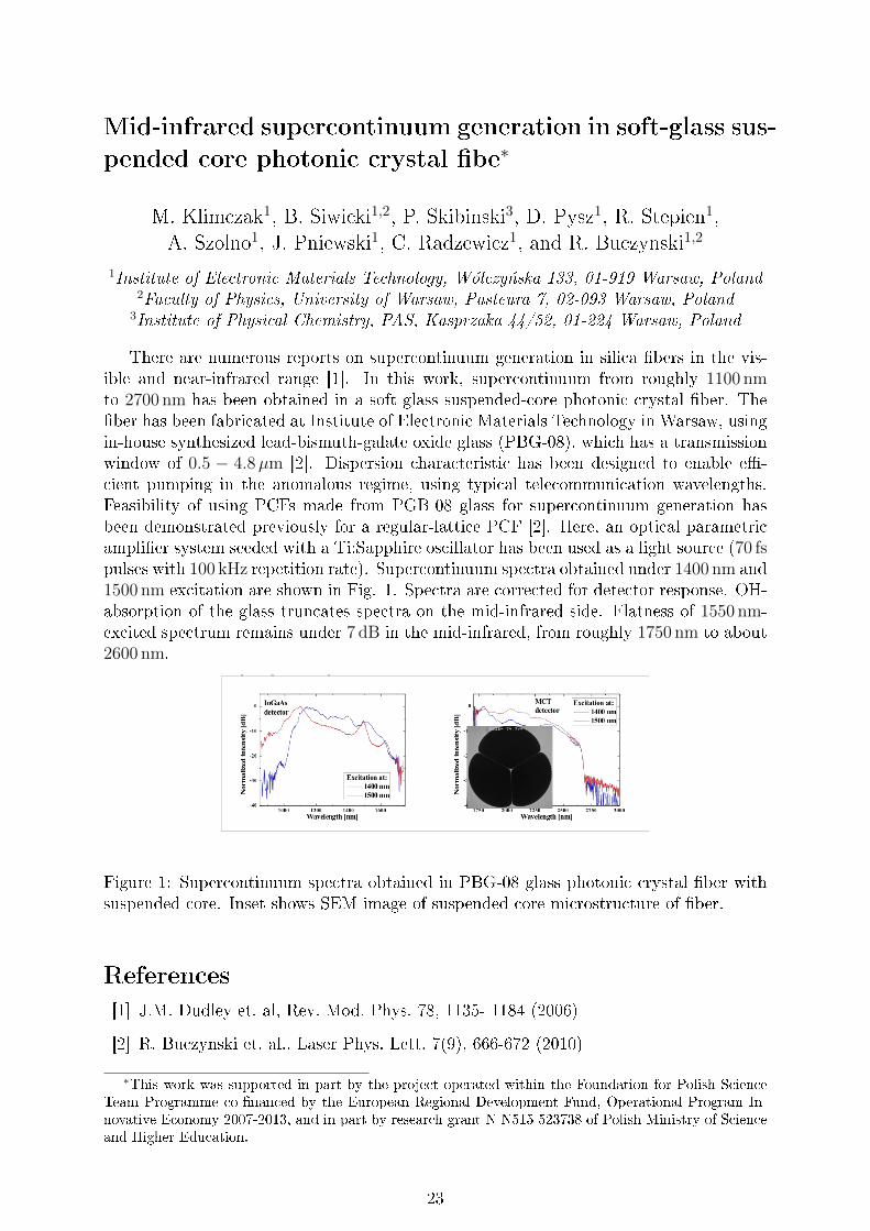
Mid-infrared supercontinuum generation in soft-glass sus-
pended core photonic crystal be∗
M. Klimczak1, B. Siwicki1,2, P. Skibinski3, D. Pysz1, R. Stepien1,A. Szolno1, J. Pniewski1, C. Radzewicz1, and R. Buczynski1,2
1Institute of Electronic Materials Technology, Wólczy«ska 133, 01-919 Warsaw, Poland2Faculty of Physics, University of Warsaw, Pasteura 7, 02-093 Warsaw, Poland
3Institute of Physical Chemistry, PAS, Kasprzaka 44/52, 01-224 Warsaw, Poland
There are numerous reports on supercontinuum generation in silica bers in the vis-ible and near-infrared range [1]. In this work, supercontinuum from roughly 1100 nmto 2700 nm has been obtained in a soft glass suspended-core photonic crystal ber. Theber has been fabricated at Institute of Electronic Materials Technology in Warsaw, usingin-house synthesized lead-bismuth-galate oxide glass (PBG-08), which has a transmissionwindow of 0.5 − 4.8µm [2]. Dispersion characteristic has been designed to enable e-cient pumping in the anomalous regime, using typical telecommunication wavelengths.Feasibility of using PCFs made from PGB-08 glass for supercontinuum generation hasbeen demonstrated previously for a regular-lattice PCF [2]. Here, an optical parametricamplier system seeded with a Ti:Sapphire oscillator has been used as a light source (70 fspulses with 100 kHz repetition rate). Supercontinuum spectra obtained under 1400 nm and1500 nm excitation are shown in Fig. 1. Spectra are corrected for detector response. OH-absorption of the glass truncates spectra on the mid-infrared side. Flatness of 1550 nm-excited spectrum remains under 7 dB in the mid-infrared, from roughly 1750 nm to about2600 nm.
Figure 1: Supercontinuum spectra obtained in PBG-08 glass photonic crystal ber withsuspended core. Inset shows SEM image of suspended core microstructure of ber.
References
[1] J.M. Dudley et. al, Rev. Mod. Phys. 78, 1135- 1184 (2006)
[2] R. Buczynski et. al., Laser Phys. Lett. 7(9), 666-672 (2010)
∗This work was supported in part by the project operated within the Foundation for Polish ScienceTeam Programme co-nanced by the European Regional Development Fund, Operational Program In-novative Economy 2007-2013, and in part by research grant N N515 523738 of Polish Ministry of Scienceand Higher Education.
23

Limits of Broadband THz Detectors Based on Plasma
Oscillations in Field Eect Transistors
W. Knap1,2, D. Coquillat1 ,N. Dyakonova1, S. Rumyantsev1,3,M.S. Vitiello4, S. Blin5, and T. Nagatsuma6
1Laboratoire Charles Coulomb Université Montpellier 2 34950 Montpellier, France2Institue of High Pressure Physics UNIPRESS PAN, 02-845 Warsaw, Poland
3Rensselaer Polytechnic Institute, Troy, New York 12180, USA4NEST, Istituto Nanoscienze CNR and Scuola Normale Superiore, 56127 Pisa, Italy
55IES & TERALAB, Universite Montpellier 2 CNRS, 34950 Montpellier, France6Graduate School of Engineering Science, Osaka University, Toyonaka, Osaka, Japan
Nanometer size eld eect transistors can operate as ecient resonant or broadbandterahertz detectors, far beyond their fundamental cut-of frequencies [1]. We present anoverview of some important and recent results concerning the physics of nanometer scaleeld eect transistors used as the detection of terahertz radiation.
The subjects were selected in a way to stress some new aspects/developments ratherthan purely technological/engineering improvements. The basic physics related problemslike temperature dependence of the photoresponse [2],interferences of THz signals leadingto helicity sensitive detection are presented [3].
Until now most of works on nanometer FETs detectors were considering only THzimaging applications. We show the progress in overcoming the loading problems anddemonstrate rst results on the application of nanometer FETs as detectors in wirelesscommunication with signal modulated in GHz range [4]. Finally we present also resultsfrom THz detection by grapheme transistors [5]. A possible development of future THzdetectors using grapheme structures is also addressed.
References
[1] W. Knap and M. I. Dyakonov, `Field eect transistors for terahertz applications' inD. Saeedkia, Handbook of terahertz technology for imaging, sensing and communi-cations, Cambridge, Woodhead Publishing, 121-155 (2013)
[2] Klimenko O A, Knap W, Iniguez B, Coquillat D, Mityagin Y A, Teppe F, DyakonovaN, Videlier H, But D, Lime F, Marczewski J, and Kucharski K, J. Appl. Phys. 112,014506 (2012)
[3] Drexler C, Dyakonova N, Olbrich P, Karch J, Schafberger M, Karpierz K, MityaginYu, Lifshits M B, Teppe F, Klimenko O, Meziani Y M, Knap W and Ganichev S D,J. Appl. Phys. 111 124504 (2012)
[4] Blin S, Teppe F, Tohme L, Hisatake S, Nouvel P, Coquillat D, Penarier A, Torres J,Knap W, Nagatsuma T, IEEE El. Dev. Lett. 33 1354 (2012)
[5] Vicarelli L, Vitiello M S, Coquillat D, Lombardo A, Ferrari A C, Knap W, Polini M,Pellegrini V and Tredicucci A., Nature Materials 11 865(2012)
24
THz Time-Domain-Spectroscopy systems based on pho-
toconductive components made from GaAsBi∗
A. Krotkus1, V. Pa£ebutas1, A. Bi£iunas1, A. Koroliov1, R. Adomavi£ius1,R. Butkute1, A. Urbanowicz1,2, A. Arlauskas1, B. echavi£ius1, and
G. Molis2
1Center for Physical Sciences and Technology, Vilnius, Lithuania2 UAB TERAVIL, Vilnius, Lithuania
Material characteristics of dilute bismide alloy GaAs1−xBix (x ≤ 0, 14) layers grown bymolecular-beam-epitaxy relevant to the applications in THz optoelectronic componentswill be described. The structure of 1.5µm thick layers grown at relatively low substratetemperatures (300C) was characterized by XRD and AFM measurements. The energyband structure of the material was investigated by several optical techniques includingoptical absorption, photoluminescence, photomodulated reectance, and THz excitationspectroscopy [1] techniques; record narrow energy band gap of ∼ 0.65 eV was evidencedfor GaAs1−xBix with 13%Bi. Photoexcited carrier lifetimes in as-grown layers of the orderof few picoseconds and electron mobilities exceeding 2000 cm2/Vs were evidenced in as-grown layers by optical pump THz probe measurement; the lifetime became shorterthan 1 ps after their post-growth annealing [2]. Photoconductive antennas made from thebismide layers were used as THz emitters and THz detectors in time-domain-spectroscopysystems activated by femtosecond solid-state (Yb:KGW) and Yb:ber lasers emitting in1 mm spectral range. Frequency bandwidth up to 4.5 THx, signal-to-noise ratio ∼ 60 dBand high optical to THz conversion eciency of ∼ 5 · 10−4 was achieved in these systems.It has been shown that the photoconductive components made from layers can be usedas THz detectors activated also by 1.5µm and longer wavelength laser sources [3].
References
[1] A. Arlauskas and A. Krotkus, Semicond. Sc. Technol., vol. 27, No. 11, pp. 115015-21(2012)
[2] B. echavi£ius et.al, Semicond. Sc. Technol., vol. 26, No. 8, pp. 085033-8 (2011)
[3] A. Arlauskas et.al., Appl. Phys. Express, vol. 5, No. 2, pp. 022601-3 (2012)
∗This work was supported by the Research Council of Lithuania (grant no VP1-3.1-MM-07-K-01-058).
25

Modeling of InAsSb/AlAsSb nBn HOT detector's per-
formance limit
P. Martyniuk and A. Rogalski
Institute of Applied Physics, Military University of Technology, 2 Kaliskiego Str., 00-908Warsaw, Poland
The photo-detectors operating in the mid-wave (MWIR 3−5µm) range of the infraredradiation (IR) and meeting the requirements for high operation temperature (HOT) con-ditions are of high demand for variety of civilian and military applications. The keycondition which must be met to design the HOT IR detector is to achieve both low darkcurrent and high quantum eciency (QE). In standard p-n MWIR photodiodes operatingunder HOT conditions, the dark current is mostly produced by the Shockley-Read-Hall(SRH) generation recombination process (GR), Auger GR and both: band-to-band (BTB)and trap-assisted-tunnelling (TAT) mechanisms [1, 2].
As it was presented by Maimon and Wicks, the extrinsic SRH GR unfavourable contri-bution could be eectively reduced by the barrier's incorporation to the detectors struc-ture, while intrinsic Auger GR processes may be suppressed either by applying of thenon-equilibrium conditions or designing the detectors with materials inherently exhibit-ing lower Auger GR rates [3]-[7].
The unipolar barrier IR detector (UBIRD) architecture has been successfully imple-mented into AIIIBV bulk family compounds and InAs/GaSb type II superlatices (T2SLs)with AlGaSb/T2SLs barriers suppressing BTB tunnelling mechanism and intrinsic AugerGR process. The InAs/GaSb T2SLs preliminary success has resulted from the uniqueinherited capabilities of the new material with completely dierent physical properties incomparison with the constituent layers and what is most important, the zero valance bandosets (VBO) leading to the advantageous UBIRD band alignments slightly harder to at-tain in AIIIBV bulk compounds and much more dicult in HgCdTe [8]-[11]. Although thephysical properties indicates a potential T2SLs' superiority over bulk materials, T2SLs'InAs/GaSb development is limited by technological problems connected with the growthof uniform and thick enough SLs [12]. Additionally, the short minority carrier lifetimes(τDIF , τGR < 10 ns in temperature range > 200 K) may impede the development of theT2SLs IR devices [13, 14].
Even though HgCdTe does not exhibit a zero VBO (nested type I heterojunctionresponsible for undesired minority carrier blocking) UBIRD (nBnn) architecture was suc-cessfully adapted to the HgCdTe alloy presenting technological advantages over the reg-ular p-n HgCdTe homo-junction (simplifying the fabrication process and circumventingthe potential problems with p-type in situ doping in MBE epitaxial growth) [15]-[17].
Currently, among the barrier structures, AIIIBV bulk compounds, especially InAsSb,emerged to play a dominant role in the designing of the UBIRD detectors due to a nearlyzero VBO with respect to AlAsSb (e.g. InAs1−zSbz-cap layers, InAs1−ySby-active region,AlSb1−xAsx-barrier) [18]. In addition, InAsSb exhibits lower Auger GR rates in compar-ison to the HgCdTe [19]. Thanks to the availability of lattice matched semiconductors(GaSb, GaAs, InAs) with various band osets, the InAsSb provides additional bandengineering exibility with low level of dislocations ∼ 107 sm−2 [20, 21]. Even thoughtheoretical predictions place T2SLs in front of the IR systems' development, the better
26

stability over large area, higher electron and hole mobility and availability of high qualityand low cost substrates and fully developed technology favours InAsSb bulk family inMWIR range [22, 23].
References
[1] A. Rogalski, Infrared Detectors, second edition, CRC Press, Boca Raton (2011).
[2] A. Rogalski, Rep. Prog. Phys. 68, 2267-2336 (2005).
[3] S. Maimon and G. Wicks, Appl. Phys. Lett. 89, 151109-1-3 (2006).
[4] T. Ashley, C.T. Elliott, Electron. Lett. 21(10), 451-452 (1985).
[5] Z. Jaksic, Z. Djuric, Electronics 8(1), 30-32 (2004).
[6] S. Velicu at al., J. Electron. Mater. 39(7), 873-881 (2010).
[7] A. Itsuno at al., IEEE Trans. Electron Dev. 58(2), 501-507 (2011).
[8] A. Rogalski and P. Martyniuk Infrared Physics & Technol. 48, 39-52 (2006).
[9] J.B. Rodriguez at al., Appl. Phys. Lett. 91, 043514-1-2 (2007).
[10] D. Z.-Y. Ting at al., in Semiconductors and Semimetals, Vol. 84, pp. 1-57, edited byS.D. Gunapala, D.R. Rhiger, and C. Jagadish, Elsevier, Amsterdam (2011).
[11] A. M. Itsuno at al., Appl. Phys. Lett. 100, 161102 (2012).
[12] S. Myers at al., Proc. SPIE 8155, 815507-1 (2011).
[13] P. Martyniuk at al., Semicond. Sci. Technol. 27, 055002 (2012).
[14] J. Wróbel, at al., Proc. SPIE 8353, 8353-16 (2012).
[15] A. M. Itsuno at al., J. Elect. Mater., 40, 1624-1629 (2011).
[16] S. Velicu at al., Proc. SPIE. 8268, 82682X (2012).
[17] P. Martyniuk, A. Rogalski, Solid-State Electronics, 80 96-104 (2013).
[18] P. Klipstein, Proc. SPIE. 6940, 69402U-1-11 (2008).
[19] E. R. Youngdale, at al., Appl. Phys. Lett. 64, 3160-3162 (1994).
[20] P. Klipstein, at al., Proc. SPIE 8012, 80122R (2011).
[21] E. Weiss at al., Journal of Crystal Growth 339, 31-35 (2012).
[22] W. Vincent at al., J. Appl. Phys. 69 (6) (1990).
[23] E. Plis at al., Proc. SPIE 7945, 79451R (2011).
27

Fourier Transformed infrared modulation spectroscopy∗
M. Motyka1, F. Janiak1, G. S¦k1, and J. Misiewicz1
1Institute of Physics, Wrocªaw University of Technology, Wybrze»e Wyspia«skiego 27,50-370 Wrocªaw, Poland
Modulation spectroscopy, due to its absorption and dierential character, is an excel-lent tool to study the energies of optical transitions in quantum well(QW) and quantumdots as well as energies of bulk-like QW barriers or intermediate layers. Such experimentshave already been successfully employed to study GaSb-based QWs for infrared applica-tions up to 3µm [1] and including type II structures for even longer wavelengths [2]. Dueto a growing interest and necessity to investigate structures designed for operation in midand far infrared range (as infrared detectors, quantum cascade lasers, etc.) it has beenproposed to exploit modulation spectroscopy realized by using Fourier-transform spec-trometer [3, 4]. This approach has already been used to investigate mainly the bulk-likematerials and layers. In this work, we demonstrate the application of FTIR modulationspectroscopy (called FTPR) for the investigation of low-dimensional structures for midinfrared spectral region even beyond 5µm [4]. In addition, we introduce a new exper-imental approach called Fast Dierential Reectance (FDR) [5]. This technique allowsrecording the photoreectance-like spectra similar to those obtained in conventional mea-surements utilizing the lock-in amplication technique. In FDR approach however, thetime of collecting the spectra can be reduced from hours to seconds in comparison tostandard grating-based method. Its functionality and comparison to FTPR and FTPLwill be demonstrated for HgCdTe layers in the range of 5− 15µm [6], GaInAsSb layers onInAs [7], and long wavelength type type II AlSb/InAs/GaInSb/InAs/AlSb QW's grownon GaSb [8] and InAs.
References
[1] M. Motyka, et al., J. Appl. Phys. 106, 066104 (2009)
[2] M. Motyka, et al., Appl. Phys. Lett. 94, 251901 (2009)
[3] T.J.C. Hoseaet al., Phys. Stat. Sol.(A) 202, 1233 (2005)
[4] M. Motyka, et al., Appl. Phys. Exp. 2 (12) 126505 (2009)
[5] M. Motyka, J. Misiewicz, Appl. Phys. Express 3, 112401(2010)
[6] M. Motyka, et al., Measurement Science Technology 22, 125601(2011)
[7] M. Motyka, et al., Appl. Phys. Lett. 100, 211906 (2012)
[8] M. Motyka, et al., Optical Materials 34, 1107-1111(2012)
∗This work was partially supported by the National Science Center within the Grant DEC2011/03/D/ST3/02640 and also by Project WIDELASE, Monolithic Widely Tunable Interband CascadeLasers for Safety and Security, 7-th European Union Framework Program
28

Current state of the VECSEL development in ITE∗
J. Muszalski, A. Broda, A. Wójcik-Jedli«ska, P. Gutowski, A. Jasik,A. Trajnerowicz, I. Sankowska J. Kubacka-Traczyk, K. Goªaszewska
Instytut Technologii Elektronowej, al. Lotników 32/46, 02 668 Warszawa, Poland
In this paper we report the development of a Vertical External Cavity Surface EmittingLaser (VECSEL) carried out in ITE. Using a heterostructures grown by molecular beamepitaxy we have set up a laser emitting at 980 nm wavelength range with a maximum powerof 3.8 W. The laser was operated in a simple linear cavity with an output coupler mirrorwith the reectivity equal to 93%. The heat extraction was realized by the attachmentby liquid capillary method a synthetic diamond plate.
The design of the heterostructure applied in the reported laser was based on accu-mulated experience. The VECSEL heterostructure was deposited on GaAs substrate ina standard way i.e., the Distributed Bragg Reector (DBR) was deposited directly on asubstrate then the active region followed by the window layer and protective cap. TheDBR consisted from 27 pairs of the AlAs/GaAs quarter wavelength layers. The binarycomposition of the layers was chosen for their high heat conductivity coecient. The ac-tive region consisted of 12 In0.2Ga0.8As quantum wells (QW) embodied in a GaAs. For anecient strain compensation the 30 nm thick GaAs0.92P0.08 layers were added at both sidesof each quantum well. The QWs were uniformly spread over the microcavity accordingto the periodic resonant gain approach. The large, 13/2λ (∼ 1900 nm) cavity permittedfor ecient absorption of the pump radiation λ = 808 nm. The window, half-wavelengthlayer consisted of Al0.2Ga0.8As and was covered with 10 nm of GaAs as a protective cap.
The spectral detuning between the photoluminescence emission and the Fabry-Perotresonator was established to be 35 nm. Such high spectral detuning permits for the deviceoperation at elevated temperature.
∗Acknowledgments the reported research was supported by the grants of NCBiR NR 02 0023 06 andNCN N N515 360636
29
Direct and indirect carbonation level estimation using
MIR sensing
T.J. Ochalski1,
1Centre for Advanced Photonics & Process Analysis, Cork Institute of Technology,Ireland
In this work two methods of measurement for CO2 content in beverages will be pre-sented. An indirect method is based on measurement of the partial pressure of CO2 gasin the headspace of a PET bottle, which stays in equilibrium with dissolved CO2 in thebeverage. At a constant temperature, the amount of a given gas that dissolves in a giventype and volume of liquid is directly proportional to the partial pressure of that gas inequilibrium with that liquid. Carbonation level is then calculated using Henry's law.
The system is based on the principle of light transmission, which facilitates a directmeasurement of the CO2 present in the bottle headspace. This measurement can then berelated to the partial pressure of CO2 and ultimately the beverage's CO2 content.
Our system incorporates a PET non-uniformity thickness correction system (NUTC)to accommodate positioning and bottle to bottle variations.
A direct method uses an Attenuated Total Reectance (ATR) Liquid Test Cell basedon Mid-Infrared Spectroscopy, which can measure the dissolved CO2 level in a beverage.The measured CO2 level is independent of the beverage color, ingredients and alcoholiccontent. As such it is a true measure of dissolved CO2.
30
Non-destructive evaluation of composite materials after
dynamic load in the terahertz range
N. Palka1, D. Miedzinska2, R. Panowicz2, M. Walczakowski1
1Military University of Technology, Institute of Optoelectronics, Warsaw, Poland2Military University of Technology, Faculty of Mechanical Engineering, Warsaw, Poland
We report on investigations of internal structure of composites materials thanks to theterahertz radiation.
During the dynamic process of the interaction between a bullet and a composite plate,the destruction of the composite appears not only in a puncture region, but also in theabundance area surrounding that point. The dimension and the character of the destruc-tion area are very important for the research of the strength properties under the dynamicload.
We report on the non-destructive investigation of two composite structures basedon glass and polyethylene bers. First material is made of epoxy composites (E-53)reinforced with glass mat with the density of 316 g/m2. The beveling angle of the layersin the sample was 45. The total thickness of the sample was 10 mm.
In the second structure, the layers are created with the use of the polyethylene bersand then joint together. During the iso-static compression process carried out in the spe-cic temperature, the layers are joint together and the non resin composite is developed.The compression process as well as the type of connection between layers and the bersproperties decide about the mechanical characteristics of the new material.
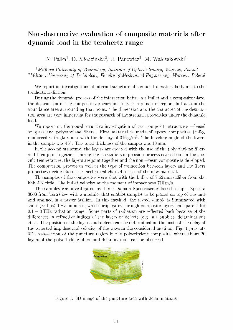
The samples of the composites were shot with the bullet of 7.62 mm caliber from thekbk AK rie. The bullet velocity at the moment of impact was 710 m/s.
The samples was investigated by Time Domain Spectroscopy-based setup Spectra3000 from TeraView with a module, that enables samples to be placed on top of the unitand scanned in a raster fashion. In this method, the tested sample is illuminated withshort (∼ 1 ps) THz impulses, which propagates through composite layers transparent for0.1 − 3 THz radiation range. Some parts of radiation are reected back because of thedierences in refractive indices of the layers or defects (e.g. air bubbles, delaminationsetc.). The position of the layers and defects can be determined on the basis of the delay ofthe reected impulses and velocity of the wave in the considered medium. Fig. 1 presents3D cross-section of the puncture region in the polyethylene composite, where about 20layers of the polyethylene bers and delaminations can be observed.
Figure 1: 3D image of the puncture area with delaminations.
31

Coupled polaritons and antipolaritons in dispersive gain
media∗
M.F. Pereira1
1Materials and Engineering Research Institute, Sheeld Hallam University. Sheeld,UK
In this paper we predict how a material excitation with a dispersive gain prole coupleswith light in a microcavity. We show that even a single transition yields an interactingset of coupled intersubband polariton [1] and antipolariton [2] branches (see Fig.1) whichcan potentially lead to a new level of all-optical control and switching in a microcavity.In contrast to the conventional antipolariton case with an imaginary Rabi frequency, thedilute nitride quantum wells chosen [3] show ample exibility to engineer the dispersivegain shape without global inversion and have potential for real Rabi frequencies withmeasurable oscillations, suggesting this as the medium of choice to investigate the couplingof photonic modes with an excitation delivering dispersive gain.
Figure 1: Coexisting antipolariton and polariton branches for (N1,N2) = (1, 1)×1011cm−2.The corresponding imaginary part of the susceptibility is shown in the inset. In thenotation of Ref. [3] the transitions are between subbands e3+ (2) and e1− (1) of a 7 nmGa0.98N0.02As-Al0.3Ga0.7As quantum well.
References
[1] D. Dini, R. Köhler, A. Tredicucci, G. Biasiol, and L. Sorba, Phys. Rev. Lett. 90116401 (2003).
[2] M.F. Pereira Jr., Phys. Rev. B75, 195301 (2007).
[3] M.F. Pereira Jr and S. Tomi¢, Appl. Phys. Lett. 98, 061101 (2011).
∗The author acknowledges support from MPNS COST ACTION MP1204 TERA-MIR Radiation:Materials, Generation, Detection and Applications and input dilute nitride bandstructure provided by S.Tomi¢.
32
THz intervalence antipolaritons∗
I.A. Faragai1 and M.F. Pereira1
1Materials and Engineering Research Institute, Sheeld Hallam University. Sheeld,UK
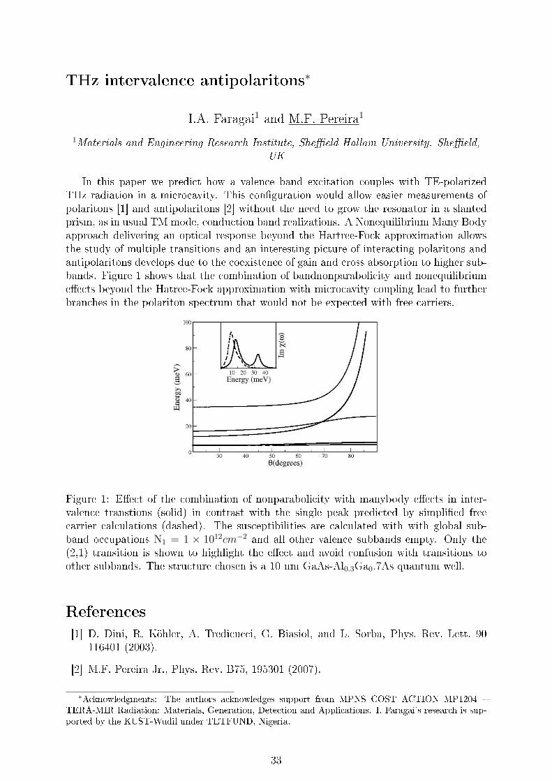
In this paper we predict how a valence band excitation couples with TE-polarizedTHz radiation in a microcavity. This conguration would allow easier measurements ofpolaritons [1] and antipolaritons [2] without the need to grow the resonator in a slantedprism, as in usual TM mode, conduction band realizations. A Nonequilibrium Many Bodyapproach delivering an optical response beyond the Hartree-Fock approximation allowsthe study of multiple transitions and an interesting picture of interacting polaritons andantipolaritons develops due to the coexistence of gain and cross absorption to higher sub-bands. Figure 1 shows that the combination of bandnonparabolicity and nonequilibriumeects beyond the Hatree-Fock approximation with microcavity coupling lead to furtherbranches in the polariton spectrum that would not be expected with free carriers.
Figure 1: Eect of the combination of nonparabolicity with manybody eects in inter-valence transtions (solid) in contrast with the single peak predicted by simplied freecarrier calculations (dashed). The susceptibilities are calculated with with global sub-band occupations N1 = 1 × 1012cm−2 and all other valence subbands empty. Only the(2,1) transition is shown to highlight the eect and avoid confusion with transitions toother subbands. The structure chosen is a 10 nm GaAs-Al0.3Ga0.7As quantum well.
References
[1] D. Dini, R. Köhler, A. Tredicucci, G. Biasiol, and L. Sorba, Phys. Rev. Lett. 90116401 (2003).
[2] M.F. Pereira Jr., Phys. Rev. B75, 195301 (2007).
∗Acknowledgments: The authors acknowledges support from MPNS COST ACTION MP1204 TERA-MIR Radiation: Materials, Generation, Detection and Applications. I. Faragai's research is sup-ported by the KUST-Wudil under TETFUND, Nigeria.
33

Components for thulium-doped ber lasers∗
P. Peterka1, P. Honzátko1, M. Písa°ík2, F. Todorov1, Y. Baravets1,O. Podrazký1 and I. Ka²ík1
1Institute of Photonics and Electronics, Academy of Sciences of the Czech Republic, v.v. i., Chaberská 57, 182 51 Prague, Czech Republic
2 SQS Vláknová optika a. s., Komenského 304, 509 01 Nová Paka, Czech Republic
Thulium-doped ber lasers operating at wavelengths around 2 micrometers are rapidlydeveloping coherent light sources with a high slope eciency reaching 70% and thus theyare challenging the well-established ytterbium-doped ber lasers operating at around1 micrometer. Two-micrometer radiation sources have many advantages over the one-micrometer sources, e.g., better eye-safety, relaxed non-linear limits and often more e-cient material processing. One particularly important application of 2-micrometer berlasers is a highly-ecient generation of wideband mid-infrared radiation through thirdorder nonlinear eects in soft-glass bers.
In this paper we will review our recent progress in developing thulium-doped berlasers, e.g., in coherent-beam combination [1] and monolithic conguration of the lasercavity. A special attention will be given to the components for such ber laser. Detailsabout preparation and characterisatons of the thulium-doped ber as well as the wave-length division multiplexers will be presented. The transmission of the fabricated WDMis shown in Fig. 1.
Figure 1: Transmission characteristics of the developed WDM 1600/1950 nm.
References
[1] P. Honzatko, Y. Baravets, F. Todorov, P. Peterka, and M. Becker, Coherently com-bined 20 W at 2000 nm from a pair of thulium-doped ber lasers, submitted forpublication in Laser Physics Letters.
∗The Authors acknowledge fruitfull cooperation with experts from Gooch & Housego in Torque, UK.The work was supported by the Czech Science Foundation project No. P205/11/1840, by the Europeanactions COST TD1001 and MP1204, and by the Ministry of Industry and Trade of the Czech Republic,project No. FR-TI4/734.
34

Uncooled mid and longwavelength infrared detectors
A. Piotrowski, and J. Piotrowski
VIGO System S.A., 129/133 Pozna«ska St. Ozarow Mazowiecki, 05-850, Poland
Status of the technology in sensitive and fast-response detection of the mid-infraredradiation with devices based on variable gap HgCdTe heterostructures working withoutcryocooling. HgCdTe heteorostructures were grown using MOCVD on GaAs substrates[1]. Recent eorts were concentrated on performance approaching fundamental limitsfor whole 2 − 13µm range, the extension of useful spectral range above 13µm and sub-nanosecond response time [2].
References
[1] A. Piotrowski et al., Optoelectron. Rev. 12, 453-458, 2004
[2] A. Piotrowski et al., Proc. SPIE 6542, 65421B1- 65421B11, 2007
35

Mid-infrared InP-based GaInNAs quantum-well VCSELs∗
. Piskorski, and R.P. Sarzaªa
Photonics Group, Institute of Physics, Lodz University of Technology, Wolczanska 219,90-924 Lodz, Poland
There is now increasing interest in room temperature (RT) continuous wave (CW)regime of the mid-infrared semiconductor devices due to their possible applications suchas distant air monitoring, laser spectroscopy, medical diagnostics, thermovision measure-ments, and wireless optical communication. Semiconductor lasers emitting radiation ofwavelengths longer than 2µm are currently grown on GaSb substrates [1]. However, theirmanufacturing is relatively expensive, complex and performance of these lasers is still farfrom the expected one. The alternate substrate material is InP [2] which is much cheaperthan GaSb. Furthermore, InP-based devices can be manufactured using well known,much simpler and less expensive technology. Therefore there is a wide interest to replacein the above applications the GaSb-based lasers with the InP-based ones produced, forexample, using diluted nitrides as InNAs, GaInNAs and GaInNAsSb. These materialshave some unusual properties in comparison with most of known semiconductors [3]. Anincrease in their nitride contents leads to reductions of both the lattice constant and theenergy gap [4]. Therefore, choosing properly the mole fractions of indium and nitrogen,the strain within these nitride structures and their band gaps can be controlled as far asthe layer thickness remains below a critical limit for creation of mist dislocations. In theGaAs-based vertical-cavity surface-emitting lasers (VCSELs), their application enablesreaching both the 1.31-µm and the 1.55-µm emission bands [5] used in the ber opticalcommunication. With the advanced InP-based technology, on the other hand, it seemsto be possible reaching even the 3.5-µm emission. An attempt to reach in InP-basedGaInNAs quantum-well (QW) laser emission wavelength longer than 2µm has been justpublished [2].
In this paper we investigate a possibility of reaching a RT CW operation of 2.33-µmand 2.6-µm in InP-based GaInNAs QW VCSELs. Because of strong absorption of thisradiations by carbon monoxide and hydrogen sulde, respectively, such VCSELs may beused in distant detection of these poisonous gases.
References
[1] Z. Yin et al., Solid-State Electronics 51, 6-15 (2007)
[2] R.P. Sarzaªa et al., Applied Physics A 108, 521-528 (2012)
[3] M. Henini, Dilute Nitride Semiconductors (Elsevier Ltd., Oxford, 2005)
[4] M. Kondow et al., Japanese Journal of Applied Physics 35, 1273-1275 (1996)
[5] H.-P. D. Yang et al., Semiconductor Science and Technology 20, 834-839 (2005)
∗This work has been partially supported by the COST Action MP0805, Polish Ministry of Scienceand Higher Education (MNiSzW) grant no. N N515 533338, and by the Polish-Singapore grant no.1/3/POL-SIN/2012
36

Overview of real-world Terahertz applications
A. Portieri12
1TeraView Limited2Rice Laser Science Group, Rice University, MS366, 6100 Main St., TX 77005 Houston,
USA
This talk will discuss advances in the use of terahertz light from the research arenatowards real world applications in industry. Demonstrating work initially developed formeasuring pharmaceutical tablet coatings, applications within automotive and industrialpaint and coating applications will be discussed.
TeraView has been developing terahertz technology and applications for over 10 yearsin several industries. Rapid, non-destructive and non-contact, low power terahertz lightpulses can accurately measure individual layer thickness of a multiple layer paint coatingand can be used to rapidly scan large areas with multiple readings. Coating layers aswell as compressed ingredients into matrix of tablets can be observed based on an opticaldelay of THz pulse wave. A brief overview of the work carried out in a number of dierentmarkets will be presented during the presentation.
37

THz wave generation and detection using a single pho-
tomixer antenna
M. Simonetta, T. Losco, G. Giuliani
Dipartimento di Ingegneria Industriale e dell'Informazione, University of Pavia, Pavia,Italy
A revolutionary THz interferometric scheme based on photoconductive antennas isproposed. In a photoconductive antenna (PCA) the outcoming eld is generated bymodulating the photoconductance via the beating of two laser beams. If the antenna isbiased with a constant voltage drop across it, a current at THz frequencies is generated,and a THz wave is emitted.
In the newly proposed scheme, a single device is used to simultaneously generate anddetect the THz eld, which is backreected or backscattered by a remote target onto thePCA that generated it. The mean photocurrent value carries information about the pathtraveled by the THz eld from the PCA to the target and back, similarly to what alreadydemonstrated using the self-mixing conguration in a semiconductor laser.
The proposed method allows to measure the absolute distance of discontinuities inthe refractive index of the medium where the THz wave is travelling. Spectrally-resolvedbackscatter THz tomography is also possible.
38
A numerical model of carrier transport in mid-IR VEC-
SELs∗
A.K. Sokóª, and R.P. Sarzaªa
Photonics Group, Institute of Physics, ód¹ University of Technology, Wolczanska 219,90-924 ód¹, Poland
Optically pumped vertical-external-cavity surface-emitting lasers (VECSELs), alsoknown as semiconductor disk lasers (SDLs), are modern semiconductor devices, whichcombine simultaneously advantages of vertical-cavity surface-emitting lasers (VCSELs),edge-emitting lasers (EELs) and solid-state lasers [1]. Their unique properties give a pos-sibility to generate high-power radiation with low-divergent, circularly symmetric outputbeams. Moreover the external cavity enables to place additional optical elements such as:saturable absorbers for mode locking, nonlinear optical crystals for frequency doubling,optical lters for wavelength selection and tuning. Such factors cause that VECSELs cannd broad applications, for example in medical, telecom and multimedia markets.
In the paper we present our numerical model of carrier transport in mid-infraredoptically pumped VECSELs. Calculations have been carried out for the GaAs-basedVECSEL operating at 1.3µm with the GaInNAs/GaAs multi-quantum-well active region.Carrier diusion in the vertical direction has been simulated using the diusion equationfor barriers in which QWs are reduced to points and act as carrier absorbers. Carrierdensity distributions for both below- and over-threshold regimes have been determined.Excitation and material gain of the individual QWs in the active region has been analyzed.Moreover a simple optical model based on the transfer-matrix method (TMM) has beenused to calculate power transfer characteristics for the considered laser.
We believe that numerical model described in this paper may give an opportunityto understand more deeply details of VECSEL operation and to design optimal mid-IRVECSEL structures.
References
[1] M. Kuznetsov, In: O.G. Okhotnikov (Ed.), Semiconductor Disk Lasers: Physics andTechnology (Wiley-VCH Verlag, Weinheim 2010), pp. 1-71
∗This work was partially supported by: the Polish-Singapore grant no. 1/3/POL-SIN/2012, theCOST Action MP0805 and by the Faculty of Technical Physics, Information Technology and AppliedMathematics, Lodz University of Technology as the grant for scientic research serving the developmentof young scientists in 2012.
39
Thin disk low voltage normal incidence single quantum
well mid-infrared modulator operating in retro-reection
mode
J. Stiens1, W. Vandermeiren1, G. Shkerdin2, C. De Tandt1 and R. Vounckx1
1Laboratory for Micro- and Photonelectronics, ETRO-FirW, Vrije Universiteit Brussel,Pleinlaan 2, B-1050 Brussels, Belgium
2Institute of Radio Engineering and Electronics of the Russian Academy of Science,Vvedenskogo Square 1, 141120 Fryazino (Moscow region), Russia
An mid-infrared modulator conceived as a thin disk modulator operating under nor-mal incidence and in retro-reection mode of which the working principle is based onevanescent wave generation and intersubband transitions in the conduction band of asingle AlGaAs/GaAs quantum well is presented. Light at normal incidence is coupledto an evanescent wave by means of a sub-wavelength diraction grating. The stronglyconned electromagnetic eld of the resulting evanescent wave can be eectively absorbedin the presence of an electron plasma in the quantum well. Modulation of the 0th orderreective mode of the structure is achieved by applying an external electrical eld acrossthe quantum well. Diraction eciency calculations were performed in order to nd thedesign parameters which results in a maximum modulator's extinction ratio. We showthat design parameters should be chosen close to Wood's anomaly. Two wafers with dif-ferent grating parameters were fabricated and tested. Experiments were conducted in the10µm wavelength range. Contrast ratios from 1.5 to 2 for about 20 V at a wavelength of10.6µm could be observed, depending on the structure. The experimental results are ingood agreement with our model and diraction eciency calculations.
40

Mid infrared ber-coupled QCL-QEPAS sensor
V. Spagnolo1, P. Patimisco1, S. Borri1, G. Scamarcio1, B.E. Bernacki2, andJ. Kriesel3
1Dipartimento Interateneo di Fisica, University and Politecnico of Bari, CNR-IFN UOSBARI, Via Amendola 173, Bari, Italy
2Pacic Northwest National Laboratory, 902 Battelle Boulevard, Richland, WA, USA3Opto-Knowledge Systems Inc., 19805 Hamilton Ave., Torrance, CA, USA
Enhanced versatility of quartz enhanced photoacoustic spectroscopy (QEPAS) sensorsystems can be obtained via optical ber delivery and coupling. Previously, small sizesensors with simple optical alignment have been realized employing a ber-coupled system(incorporating QTF, acoustic resonator, and pre-aligned ber focuser) between a near IRlaser source and QEPAS spectrophones. The feasibility to extend this approach also tomid-IR light sources will allow compact integration with very promising sources suchas quantum cascade lasers (QCLs). However, due to limited availability of mid-IR singlemode bers, the implementation of ber-coupled based QCL sensors has only very recentlybeen reported [1].
We will describe an innovative spectroscopic system based on the QEPAS techniqueusing an external cavity QCL coupled with a single mode mid-IR ber optic. SF6 hasbeen selected as a target gas in demonstration of the system for trace gas sensing. Sin-gle mode laser delivery through the prongs of the quartz tuning fork (QTF) has beenobtained employing a hollow waveguide ber with inner Ag-AgI coatings and internalcore diameter of 30µm. A detailed design and realization of the QCL ber coupling andoutput collimator system allowed almost practically all (99.4%) of the laser beam to betransmitted through the spectrophone module, which led to a strong reduction in QEPASsignal interference patterns. Experiments have been performed employing a wavelengthmodulation technique by applying a sinusoidal modulation to the diode laser currentat half of the QTF resonance frequency f0/2 and detecting the QTF response at f0 bymeans of a lock-in amplier. Taking advantage of the very fast V-T relaxation rate andthe strong absorption strength of SF6, we achieved a record QEPAS sensitivity of 50 partsper trillion in 1 second, corresponding to a record for QEPAS normalized noise-equivalentabsorption of 2.7 · 10−10 W · cm−1 · Hz−1/2.
References
[1] V. Spagnolo et al., Opt Lett. 37, pg. 4461-4463 (2012)
41

Dilute bismides for infrared optoelectronics applications
S. Wang12
1Shanghai Institute of Microsystem and Information Technology, Chinese Academy ofSciences 865 Changning Road, Shanghai 200050, China
2Department of Microtechnology and Nanoscience, Chalmers University of Technology41296 Goteborg, Sweden
Dilute bismide is the least studied III-V compounds with many interesting physicalproperties. We report some recent progresses on epitaxial growth of III-AsBi and III-SbBi and the Bi surfactant eect. The growth window is found very narrow. Bismuth isfound to be incorporated at both substitutional and interstitial sites in GaSbBi. It alsoinduces signicant In and Ga inter-diusion at the GaSb/InSb interface. As a surfactant,Bi can extend the critical thickness of InGaAs on GaAs substrates and enhance lumines-cence intensity. We also discuss the thermal stability issue which is critical for practicaloptoelectronic devices.
42

Modelling Gain under Operation in Quantum Cascade
Lasers
D.O. Winge, M. Lindskog, A. Wacker
Mathematical Physics, Lund University, Box 118, Lund 22100, Sweden
We report a theoretical study, in which we calculate the nonlinear response of a bi-ased quantum cascade laser (QCL) under high intensity radiation. The calculations arebased on the nonequilibrium Green's function formalism including both the stationarybehavior Green's functions, and the part of the response that vary in time according tothe oscillating electromagnetic eld [1].
Assuming a periodic behavior in the response as well, the Fourier components of theresponse are calculated, and the dynamics of the system is thus expressed in a Fourierseries with the fundamental response and its higher harmonics. By including at rst onlythe fundamental and the most prominent harmonics, the ones of low order, we can thenincrease the accuracy of the method by including even higher harmonics, needed for highintensity calculations.
The calculations are done on a four well resonant-phonon QCL that has been studiedby Burgho et al. where the gain of the structure was successfully measured [2]. In ourwork we compare the ndings of the simulations to their measurements and nd that thehigh intensity calculations of the non linear response agrees best with the experimentaldata. This suggests that the intensity used in the experimental measurements do notcorrespond to linear response. By relating the response of the system at dierent biasesand external light eld intensities a theoretical connection to gain clamping is also beestablished, and the output power approaching the operating point calculated and relatedwith good agreement to the experiment [3].
Figure 1: Gain calculated at two dierent biases (a, b) and at dierent eld strengths,given by eFacd where e is the electron charge, Fac the external eld strength and d is theperiod length. The intensity of the light eld resulting in gain at the clamping level isthen assumed to be related to the output power of the QCL
References
[1] A. Wacker et al., IEEE J. Sel. Topics. Quantum Electron. (to be published)
[2] D. Burgho et al., Appl. Phys. Lett. 98, 061112 (2011)
[3] D. O. Winge, M. Lindskog and A. Wacker, Appl. Phys Lett. 101, 211113 (2012)
43

Posters
44
Characterization of microlenses made of tellurite and
heavy metal oxide glass developed with hot embossing
technology∗
R. Kasztelanic1, I. Kujawa2, R. St¦pie«2, J. Cimek2, K. Hara±ny2,M. Klimczak2, A.J. Waddie3, M.R. Taghizadeh3, and R. Buczy«ski1,3
1University of Warsaw, Faculty of Physics, Pasteura 7, Warsaw, Poland2Institute of Electronic Materials Technology, ul. Wólczy«ska 133, Warsaw, Poland3Institute of Photonics and Quantum Sciences, School of Engineering and Physical
Sciences, Heriot-Watt University, Edinburgh EH14 4AS, Scotland, UK
For about 10 years a dynamic development of research and applications of opto-electronics within the infrared (2 ÷ 14µm) spectrum has been observed [1]. Howevernovel methods for low-cost, mass fabrication of diractive and refractive optical micro-components for the mid-infrared are required [2]. We have developed refractive and dirac-tive micro lenses with the use of a hot embossing process from multi-component glasses(Fig. 1). In the experiment lead-bismuth-gallium oxide (PBG08) and tellurite glasses,which are characterized by high transmittance within the visible light spectrum to mid-infrared (up to 6.5µm), were used. A quartz element, which had been fabricated usingthe standard photolithographic/reactive ion etching processes, was used as the mouldduring the embossing process. The elements presented were fabricated in a low pressurestatic process. Their quality was examined with a white light interferometer and theiroverall performance was assessed by M2 and image resolution measurements (Fig. 2).The measured M2 for the lead-bismuth-gallium oxide refractive lenses with a focal lengthof 3.3 mm and a diameter of 3.2 mm was 2.3.
a) b)
Figure 1: Refractive (a) and diractive (b) microlenses for mid IR imaging and beamfocusing
References
[1] R. Waynant, et al., Phil. Trans. R. Soc. Lond. A 359, 635-344 (2001)∗This research is supported by the Polish MNiSW research grant N N507 431339 and the project op-
erated within the Foundation for Polish Science Team Programme co-nanced by the European RegionalDevelopment Fund, Operational Program Innovative Economy 2007-2013
45

a) b)
Figure 2: The resolution pattern 17.95 lp/mm imaged with refractive lens made of PBG08lens (a) image at focal plane of an array diractive microlenses (b).
[2] I. Kujawa, et al., Proc. of SPIE, 8428, 84281P-84281P-7 (2012)
46

Optimization of Epitaxial Structures for Terahertz Emit-
ters Based on GaN/AlGaN HEMTs∗
G. Cywi«ski1, M. Siekacz1, G. Muzioª1, K. Szkudlarek1, K. Dybko2,M. Bo¢kowski1, W. Knap1,3, and C. Skierbiszewski1
1Institute of High Pressure Physics, Polish Academy of Science, Sokoªowska 29/37,01-142 Warsaw, Poland
2Institute of Physics, Polish Academy of Sciences, al. Lotników 32/46, 02-668 Warsaw,Poland
3Laboratoire Charles Coulomb UMR 5221, Université Montpellier 2& CNRS, France
The channel of High Electron Mobility Transistor can act as a resonator for the plasmawaves propagating in 2D electron gas. The plasma frequency increases with reduction ofthe channel length and can reach the Terahertz range for nanometer size transistors. Asit was predicted by Dyakonov and Shur [1], when a current ows through a eld eecttransistor, the steady state can become unstable against generation of plasma wavesleading to the emission of an electromagnetic radiation at the plasma wave frequencies.
The last few years have brought the progress in the High Electron Mobility Transistor(HEMT) based sources and detectors of THz radiation fabricated on the nitrides epitaxialstructures. Recently THz emission was observed in dierent types of GaN/AlGaN nano-metric high electron mobility transistors. In agreement with the theoretical predictions i)the emission frequencies corresponded to the estimated plasma wave frequencies and ii)the emission appeared once the drain current exceeded a certain well dened thresholdvalue [2].
The optimization of growth is necessary for two reasons: i) observation of plasmainstabilities requires very high mobility and ii) one has to isolate the 2DEG gas fromthe parasitic substrate conductance. However the existing nitride technology for HEMTapplication suers from low carrier mobility and a current leakage on the regrowth in-terface between epitaxial layers and the substrate. In spite of dierent approaches, thesemain technological issues are still not completely resolved. In this work we address theseproblems by using plasma assisted molecular beam epitaxy (PAMBE) growth of HEMTsepilayers on very high quality substrates.
Our samples have been grown in PAMBE machine on semi insulating low dislocationdensity substrates grown at high pressure reactor [3]. We grew the HEMT epitaxial struc-tures with dierent startup layers. We have investigated the inuence of semi insulatingGaN:Mg epitaxial layer on electrical properties of test structures (hall bars). We foundthat increasing of the GaN:Mg thickness up to 0.5µm leads to electrical isolation of the2DEG with resistance between dierent devices being over 1 GΩ. The Hall measurementsperformed in the temperatures range 300-10K show high room temperature electron mo-bility (over 2100 cm2/Vs) and very good the electrical separation from the substrate. Wewere able to achieve excellent properties of 2DEG without any measurable parallel con-ductivity. On the selected samples, we have fabricated the HEMT devices with the gate
∗This work was partially supported by the European Union within European Regional DevelopmentFund, through grant Innovative Economy (POIG.01.01.02-00-008/08) and by Polish Ministry of Scienceand Higher Education Grant No. IT 13426.
47

0.254µm with good electrical characteristics. These structures are excellent candidatesfor future THz emitters.
References
[1] M. I. Dyakonov, M. S. Shur, Phys. Rev. Lett. 71, 2465 (1993).
[2] A. El Fatimy, N. Dyakonova, Y. Meziani, T. Otsuji, W. Knap, S. Vandenbrouk,K. Madjour, D.Théron, C. Gaquiere, M. A. Poisson, S. Delage, P. Prystawko, C.Skierbiszewski, J. Appl. Phys. 107, 024504 (2010).
[3] I. Grzegory, M. Bo¢kowski, B. ucznik, J. Weyher, E. Litwin-Staszewska, L. Kon-czewicz, B. Sadovyi, P. Nowakowski, S. Porowski, Journal of Crystal Growth 350, 50(2012).
48
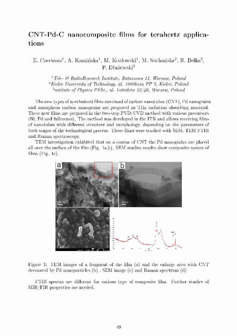
CNT-Pd-C nanocomposite lms for terahertz applica-
tions
E. Czerwosz1, A. Kami«ska1, M. Kozªowski1, M. Sucha«ska2, R. Belka2,P. Dªu»ewski3
1Tele- & RadioResearch Institute, Ratuszowa 11, Warsaw, Poland2Kielce University of Technology, al. 1000lecia PP 7, Kielce, Poland
3nstitute of Physics PASc., al. Lotników 32/46, Warsaw, Poland
The new types of synthesized lms consisted of carbon nanotubes (CNT), Pd nanograinsand amorphous carbon nanograins are proposed as THz radiation absorbing material.These new lms are prepared in the two-step PVD/CVD method with various precursors(Ni, Pd and fullerenes). The method was developed in the ITR and allows receiving lmsof nanotubes with dierent structure and morphology, depending on the parameters ofboth stages of the technological process. These lms were studied with SEM, TEM FTIRand Raman spectroscopy.
TEM investigation exhibited that on a canvas of CNT the Pd nanograins are placedall over the surface of the lm (Fig. 1a,b). SEM studies results show composite nature oflms (Fig. 1c).
Figure 1: TEM images of a fragment of the lm (a) and the enlarge area with CNTdecorated by Pd nanoparticles (b) , SEM image (c) and Raman spectrum (d)
FTIR spectra are dierent for various type of composite lm. Further studies ofMIR/FIR properties are needed.
49

Numerical calculations of SAGCM type InGaAs/InAlAs/InP
avalanche photodiode with monolithic refractive optics
K. Czuba12, J. Jurenczyk2, J. Kaniewski2
1Wrocªaw University of Technology, Faculty of Microsystem Electronics and Photonics,ul. Janiszewskiego 11/17, 50-372 Wrocªaw, Poland
2Institute of Electron Technology, al. Lotników 32/46, 02-668 Warszawa, Poland
Numerical calculations of Separate Absorption, Grading, Charge and Multiplication(SAGCM) Avalanche Photodiode (APD) based on lattice-matched InGaAs/InGaAlAs/InAlAs/InP heterostructure are presented. For modeling commercially available Tech-nology Computer Aided Design (TCAD) by SILVACO was used. In simulations severaldierent models of light propagation in multilayered structures have been considered.Obtained results comprised three device congurations: two with refractive optics, inparticular hemispherical and hyper-hemispherical lenses, and one at structure withoutlens. Electrical characteristics of these instances have been compared and discussed. Inu-ence of implementing lens and its shape on electromagnetic eld distribution and opticalparameters of the device have been depicted.
50

Infrared modulation spectroscopy for spin orbit interac-
tion determination in semiconductors∗
M. Dyksik1, M. Motyka1, F. Janiak1, J. Misiewicz1, K.D. Moiseev2
1Institute of Physics, Wrocªaw University of Technology, Wybrzeze Wyspianskiego 27,50-370 Wrocªaw, Poland
2Ioe Institute, Politekhnicheskaya 26, 194021, St Petersburg, Russia
A very important parameter, which must be taken into account in designing the laserstructures, is the spin-orbit splitting in the valence band.The resonance between the split-o valence bands and the energy of the emitted photons results in a signicant increaseof the Auger recombination rate and enhanced intervalence band absorption, which dete-riorates the luminescent characteristics of the IR-emitters operating at the 3− 5µm.
In this work, we investigate thick layers of narrow-gap InGaAsSb material with highIn content grown on InAs substrates by liquid phase epitaxy, beeing potentially able tocover spectrally the range of the waves longer than 3µm.
We present temperature dependence of photoluminescence (PL) and photoreectance(PR) spectra connected to the energy gap and the spin-orbit split o transition in InGaxAs-Sby/Ga0.84In0.16As0.22Sb0.78/InAs layers measured by the FTIR spectrometer in the midinfrared range [1, 2]. In example for Ga0.84In0.16As0.22Sb0.78/In0.83Ga0.14As0.82Sb0.17/InAs,the energy gap thermal coecient has been found to be α = −0.43 meV/K and the spinorbit interaction has been determined as ∆so = 0.460 eV. Finally, the spin-orbit splittingcompositional dependence has been recognized as a nonlinear with the negative bowingparameter C(∆0) = −0.25 eV. There are two points of the quaternary alloy compositions(InGa0.03AsSb0.06 and InGa0.93AsSb0.87) for which a resonance condition (E0 = ∆0) canbe realized at 77 K. Owing to the bandgap spin-orbit splitting resonance, the InGaAsSbmight have the unique feature of very low excess noise factor in avalanche photodiodesoperating in middle infrared spectral range
References
[1] M. Motyka, F. Janiak, M. Dyksik, Jan Misiewicz, K. D. Moiseev, Applied PhysicsExpress (2013), under review
[2] M. Motyka, F. Janiak, G. S¦k, J. Misiewicz, K.D. Moiseev, Appl. Phys. Lett.100211906 (2012)
∗This work was performed in framework of the programs of General Physics Division of RAS andPresidium of RAS and was in part supported by Russian Basic Researches Foundation (grant # 11-02-00234). In addition, M.M. would like to also acknowledge the Ministry of Science and Higher Educationfor nancial support from the Iuventus Plus program.
51
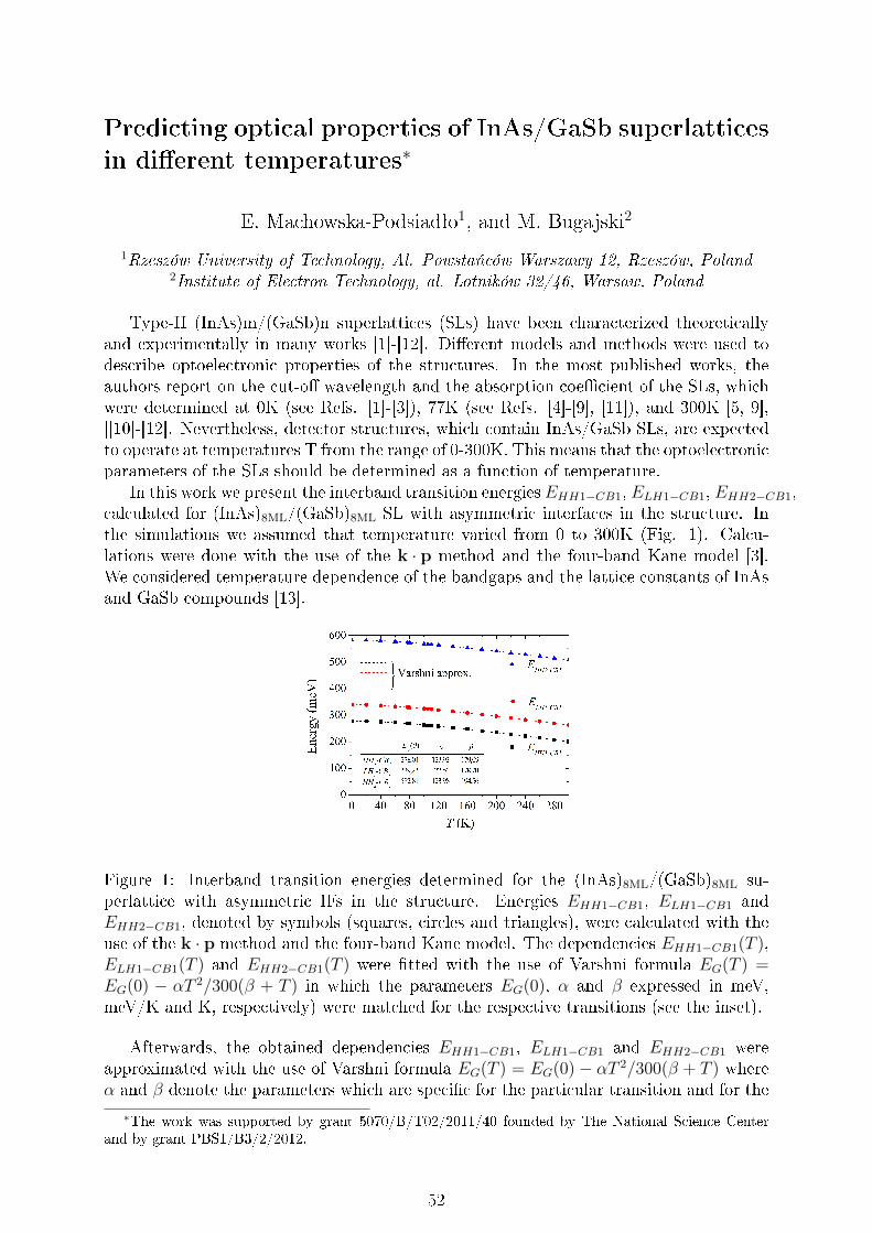
Predicting optical properties of InAs/GaSb superlattices
in dierent temperatures∗
E. Machowska-Podsiadªo1, and M. Bugajski2
1Rzeszów University of Technology, Al. Powsta«ców Warszawy 12, Rzeszów, Poland2Institute of Electron Technology, al. Lotników 32/46, Warsaw, Poland
Type-II (InAs)m/(GaSb)n superlattices (SLs) have been characterized theoreticallyand experimentally in many works [1]-[12]. Dierent models and methods were used todescribe optoelectronic properties of the structures. In the most published works, theauthors report on the cut-o wavelength and the absorption coecient of the SLs, whichwere determined at 0K (see Refs. [1]-[3]), 77K (see Refs. [4]-[9], [11]), and 300K [5, 9],[[10]-[12]. Nevertheless, detector structures, which contain InAs/GaSb SLs, are expectedto operate at temperatures T from the range of 0-300K. This means that the optoelectronicparameters of the SLs should be determined as a function of temperature.
In this work we present the interband transition energiesEHH1−CB1, ELH1−CB1, EHH2−CB1,calculated for (InAs)8ML/(GaSb)8ML SL with asymmetric interfaces in the structure. Inthe simulations we assumed that temperature varied from 0 to 300K (Fig. 1). Calcu-lations were done with the use of the k · p method and the four-band Kane model [3].We considered temperature dependence of the bandgaps and the lattice constants of InAsand GaSb compounds [13].
Figure 1: Interband transition energies determined for the (InAs)8ML/(GaSb)8ML su-perlattice with asymmetric IFs in the structure. Energies EHH1−CB1, ELH1−CB1 andEHH2−CB1, denoted by symbols (squares, circles and triangles), were calculated with theuse of the k · p method and the four-band Kane model. The dependencies EHH1−CB1(T ),ELH1−CB1(T ) and EHH2−CB1(T ) were tted with the use of Varshni formula EG(T ) =EG(0) − αT 2/300(β + T ) in which the parameters EG(0), α and β expressed in meV,meV/K and K, respectively) were matched for the respective transitions (see the inset).
Afterwards, the obtained dependencies EHH1−CB1, ELH1−CB1 and EHH2−CB1 wereapproximated with the use of Varshni formula EG(T ) = EG(0)− αT 2/300(β + T ) whereα and β denote the parameters which are specic for the particular transition and for the
∗The work was supported by grant 5070/B/T02/2011/40 founded by The National Science Centerand by grant PBS1/B3/2/2012.
52

considered SL structure. Simultaneously, EG(T ) describes an energy gap at a temperatureT, which is determined as a separation of two minibands in the SL structure, betweenwhich the transition is considered. In this work we also present the absorption coecientα calculated at the Brillouin zone center for the transitions discussed above. The obtainedvalues of α correspond to the energies EHH1−CB1, ELH1−CB1 and EHH2−CB1 , which areillustrated in Fig. 1.
References
[1] F. Szmulowicz, H. Haugan and G. J. Brown, Phys. Rev. B 69, 155321 (2004)
[2] R. Magri and A. Zunger, Phys. Rev. B 65, 165302 (2002)
[3] E. Machowska-Podsiadªo et al., J. Phys.: Conf. Ser. 367, 012014 (2012)
[4] E. Plis et al., IEEE J. Sel. Topics Quantum Electron. 12, 1269 (2006)
[5] J B Rodriguez, P Christol, F Chevrier and A Joulli, Physica E 28, 128 (2005)
[6] R. Kaspi, Ch. Moeller and A. Ongstad, Appl. Phys. Lett. 76, 409 (2000)
[7] G. C. Dente and M. L. Tilton, Phys. Rev. B 66, 165307 (2002)
[8] A. P. Ongstad et al., J. Appl. Phys. 89, 2185 (2001)
[9] A. Jasik et al., Crystal Growth: Theory, Mechanisms and Morphology. Chapter 9 -MBE Growth of Type-II InAs/GaSb Superlattices on GaSb Buer, (Nova SciencePublishers, Inc., Hauppauge NY, 2012)
[10] F. Szmulowicz, Eur. J. Phys. 25, 569 (2004)
[11] W. H. Lau and M. E. Flatte, J. Appl. Phys. 80, 1683 (2002)
[12] E. Machowska-Podsiadªo and M. Bugajski, Acta Physica Polonica A Supp. 116, 65(2009)
[13] H. Hans Landolt et al., Numerical Data and Functional Relationships in Science andTechno-logy. New Series. Group 3., edited by O. Madelung Vol.17a-b (Springer, NewYork, 1982)
53

Electronic transport through a quantum nanosystem in
a photon cavity
T. Arnold 1, Ó. Jónason 1, C.S. Tang 2, H.S. Goan 3, A. Manolescu4, andV. Gudmundsson 1
1Science Institute, University of Iceland, Dunhaga 3, IS-107 Reykjavik, Iceland2 Dept. of of Mechanical Engineering, National United University, 1, Lienda, Miaoli
36003, Taiwan3 Department of Physics and Center for Theoretical Sciences, National Taiwan
University, Taipei 10617, Taiwan4 School of Science and Engineering, Reykjavik University, Menntavegur 1, IS-101
Reykjavik, Iceland
Using a non-Markovian Master equation we describe the transport of electrons throughan open nanosystem placed in an electromagnetic cavity with one quantized photon mode.The open nanosystem is contacted to macroscopic leads having the role of electron reser-voirs. A chemical potential bias in the leads drives the electrons through the nanosystemswhere they interact with the cavity photons. The Coulomb electron-electron and the elec-tromagnetic electron-photon interactions are treated on the same footing, within the exactdiagonalization procedure, in the electron-photon many-body Fock space. Our approachdoes not rely on the traditional rotating-wave approximation and goes beyond the populartwo-level approach. The eects related to the geometry of the electronic system and thepolarization of the electromagnetic eld are explicitly taken into account. Our numericalresults demonstrate that the two-level system approximation and the Jaynes-Cummingsmodel are only valid in the weak electron-photon coupling regime. In the strong couplingcase the quadratic contribution of the vector potential may lead to signicant correctionsto the energy spectrum. We show results for the photo-transport of a short quantum wireand of a quantum ring in an external magnetic eld.
54

Protein dynamics in solutions of dierent pH values probed
by THz spectroscopy and molecular modeling∗
M. Mernea1, O. Grigore2, O. Calborean1, J. Pintea3, T. Dascalu2,D.F. Mihailescu1
1University of Bucharest, Faculty of Biology, Splaiul Independentei, Nr. 91-95, 050095,Bucharest, Romania
2National Institute for Laser, Plasma and Radiation Physics, Laboratory of Solid-StateQuantum Electronics, R-077125, Bucharest, Romania
3National Institute for R& D in Electrical Engineering ICPE-CA, Splaiul Unirii, Nr.313, 030138, Bucharest, Romania
Proteins comprise various ionizable amino acids that respond to the pH of the externalenvironment by changing their protonation state. The external pH value changes the netelectrical charge at the surface of proteins and has a strong impact on protein structure,stability and solubility [1].
Bovine serum albumin (BSA), the major protein from bovine plasma, is involved inthe binding and transport of several ions, metabolic compounds or lipids. Its confor-mation and exibility should be highly sensitive to pH and ionic strength. Since THzspectroscopy was previously successfully used to dierentiate between conformations ofthe same molecule, mutations within the same molecular species or between molecularspecies, we used THz spectroscopy to investigate the structure and exibility of BSA atdierent pH values (4, 5, 6, 7 and 8).
We rst addressed the pH inuence on BSA exibility by theoretical methods. BSAmolecules protonated according to the considered pH values were modeled based on theknown structure of BSA [2]. THz spectra of the models were simulated using normalmodes analysis following the method described in [3] and were compared in the frequencyrange comprised between 0 and 1 THz. The structure of BSA protonated according toa pH value of 4 presents the lowest theoretical THz absorption, while the highest THzabsorption was calculated for the BSA structures protonated at pH5 and 6. Despite ofthe dierences between the electrical charge of BSA at pH5 and BSA at pH6, their THzabsorption is similar. THz spectroscopy experiments performed on BSA solutions withdierent protein concentrations and pH values are in progress.
References
[1] P. Kuki¢ et al., Proteins 78, 971-984 (2010)
[2] K.A. Majorek et al., Molecular Immunology 52, 174-182 (2012)
[3] M. Mernea et al., Journal of Optoelectronics and Advanced Materials 12, 135-140(2010)
∗We acknowledge the nancial support of the Romanian Ministry of Education, Research, Youth andSport through the IDEAS project 137 / 2011: Protein three-dimensional structure and conformationaltransitions determination by high-power narrow-band THz radiation and by molecular modeling.
55

Alteration of protein structure and exibility by gly-
cation investigated by THz spectroscopy and molecular
modeling∗
O. Grigore1, M. Mernea2, O. Calborean2, T. Dascalu1, D.F. Mihailescu2
1National Institute for Laser, Plasma and Radiation Physics, Laboratory of Solid-StateQuantum Electronics, Bucharest, Romania
2University of Bucharest, Faculty of Biology, Bucharest, Romania
Modication of proteins after synthesis changes their size, charge, structure, confor-mation and function. Some of these modications occur under pathological conditions. Indiabetes, in the presence of increased and long-term persistent concentrations of glucose,proteins can undergo glycation. The glycation of human serum albumin (HSA) has anegative impact on its activity, unfolding and degradation [1].
Our aim was to investigate HSA structural and exibility changes induced by glycationon in vitro glycated HSA by THz spectroscopy and molecular modeling. For comparison,we also investigated the changes produced by glycation in bovine serum albumin (BSA),the homologous protein of HSA in cattle (70% sequence identity).
In vitro glycation of HSA and BSA in the presence of glucose and fructose was suc-cessfuly achived, as proved by electrophoretic analysis. THz spectroscopy experimentson the glycated samples are in progress. Glycation was modeled based on the known 3Dstructure of HSA [2] and on a structural model of BSA molecule [3]. Previous studieshave shown that the most susceptible glycation sites in HSA are Lys 525, 439 and 233 andthat the advanced end glycation product that occurs at these sites is pyrraline (PYR).Since in the case of BSA the glycation sites are insuciently described, we modeled theglycation of the homologous sites of those in HSA, namely Lys 524 and Lys 232. Lys 439from HSA is homologous with Thr438 from BSA. Nevertheless, the neighboring aminoacid of Thr438 in BSA is a Lys. In this situation, we built two models of glycated BSA:with PYR attached at two sites and at three sites. THz spectra of the native and glycatedproteins were simulated using the method described in [3] and were compared in the fre-quency range of 0 THz to 1 THz. Simulation results show that in the case of BSA, theaddition of PYR residues decreases the THz absorption. On the other hand, in the caseof HSA, the eect of glycation is to decrease the THz absorption of HSA in the frequencyrange of up to 0.65 THz, while it increases its absorption at the other frequencies up to1 THz.
References
[1] P. Rondeau et al., Biochemie 93, 645-658 (2011)
[2] S. Sugio et al., Protein Engineering Design and Selection 12, 439-446 (1999)
[3] M. Mernea et al., J. of Optoelectronics and Advanced Materials 12, 135-140 (2010)
∗We acknowledge the nancial support of the Romanian Ministry of Education, Research, Youth andSport through the IDEAS project 137 / 2011: Protein three-dimensional structure and conformationaltransitions determination by high-power narrow-band THz radiation and by molecular modeling.
56

Application of quantum cascade lasers to pollutant gases
detection∗
J. Wojtas, M. Miczuga, J. Mikoªajczyk, D. Szabra, M. Nowakowski,K. Kopczy«ski, and Z. Bielecki
Institute of Optoelectronics, Military University of Technology, 2 Kaliskiego Str., 00-908Warsaw, Poland
We would like to present some application ideas of quantum cascade lasers developedat the Institute of Electron Technology to pollutant gases detection. In these detectionsetups, there will be also applied mid-IR radiation detectors based on type-II superlatticesoptimized for molecular spectroscopy designed by VIGO System SA. The research anddevelopment works being the subject of the project are new ones and deal with devices,which are not commercially available.
In recent years, substantial increases in risks related to using various hazardous chem-icals are observed. Therefore early detection of this type of threats should be performed.Optoelectronic sensors employing laser absorption spectroscopy could be very useful forthis purpose. They are more sensitive and selective than many other detection techniques[1].
In the absorption spectroscopy, detection limit depends on several factors. One of themis optical path length, over which the light interacts with examined molecules. Thus, toimprove detection limit the optical path is often increased. We propose two schemes ofsuch setups. In the rst one, White type multipass cell is applied. The cell is composedof two metallic, concave mirrors. The distance between them is 0.3 m, however opticalpath length is ∼ 76 m [2]. Operation of the second setup is based on cavity enhancedabsorption spectroscopy, which is one of the most sensitive optoelectronic techniques oftrace matter detection. In this technique, there is applied an optical cavity with a highquality factor that is made up of two concave mirrors with very high reectivity. Thisresults in a long optical path, even up to a few kilometres [3].
It is well known that simple setups employing so-called direct laser absorption spec-troscopy technique attain a detection limit up to 10−4 cm−1. In comparison, practicalrealizations of the described setups will provide this limit up to 10−9 cm−1. Therefore,they could be used in some environment, military and medicine applications [4, 5].
References
[1] T. Stacewicz, et al., Opto-Electron. Rev. 20 (1), pp. 34-41, (2012).
[2] M. Miczuga, et al., Proc SPIE, Laser Techn. 2012: Appl. of Lasers, 87030E, (2013).
[3] Z. Bielecki, et al., Metrol. Meas. Syst. XIX(1), pp. 3-28, (2012).
[4] J. Wojtas, et al., Opto-Electron. Rev. 20 (1), pp. 77-90, (2012).
[5] J. Wojtas, et al., Opto-Electron. Rev. 21 (2), pp. 9-18 (2013).
∗The presented works were supported by The National Centre for Research and Development and inthe frame of the project EDEN, ID: 179616.
57
High-current driver for quantum cascade lasers
J. Mikoªajczyk, J. Wojtas, A. Prokopiuk, M. Garli«ska, Z. Bielecki
Institute of Optoelectronics, Military University of Technology, 2 Kaliskiego Str., 00-908Warsaw, Poland
The poster presents a prototype of a driver system designed to laboratory investiga-tions of quantum cascade lasers. Signicant requirements of these lasers operation, aswell as construction of the main components of the driver system were analyzed. Duringthe driver tests a tuning range of both current pulses and operation temperature weredetermined. Additionally the method of monitoring both current and voltage of the laserswere also described. As a summary, results of laboratory studies of the driver with use ofcommercial QC lasers developed by Alpes Lasers S.A. are presented.
58

Recent Results on Synthesis and Characterization of Mon-
oclinic Ag2Te Crystals∗
T.I. Milenov1 and C.W. Luo2
1Institute of Electronics, Bulgarian Academy of Sciences, 72 Tzarigradsko ChausseBlvd., 1784 Soa, Bulgaria
2Department of Electrophysics, National Chiao Tung University, No 1001, Ta Hsueh Rd,Hsinchu 300, Taiwan
Silver telluride (Ag2Te), one of silver chalcogenides, is known as the Hessite min-eral in nature. It has some unique properties such as superionic conductivity and (asit was recently shown by Zhang et al. [1]) theoretical calculations indicated that thelow-temperature phase (β-Ag2Te) was a new binary topological insulator with highlyanisotropic single Dirac cone surface.
The band-gap values of β-Ag2Te reported in literature are inconsistent and vary from0.01 up to 1.7 eV [2, 3]. Besides, the broadband optical spectrum of β-Ag2Te and therelated optical constants are missing. Moreover, the Raman spectrum is also not claried-the interested researcher could easily nd information as to what feature in the Ramanspectrum does not belongs to the Ag2Te vibrations.
We obtained β-Ag2Te crystal ingots containing few grains by the Bridgman method.We also deposited thin lms of tellurium, Ag5Te3 and (Te+Ag5Te3) by thermal evapo-ration method. The phase homogeneity of the specimens in all experiments and theircomposition were studied by SEM/EDX.
The broadband reectance spectra of β-Ag2Te crystals were measured. In the regionfrom FIR to MIR, we observed a small dip at a photon energy of about 0.008 eV andit is attributed to the free carrier absorption in the THz region [2]. In the region fromMIR to NIR, there is another dip at a photon energy of about 0.097 eV, which mightbe due to carrier-plasmon coupling. We used the Kramer-Kroing relation to analyze thecomplex dielectric function of β-Ag2Te through the reectance spectra. By calculating theabsorption coecient, we obtain an energy band gap of β-Ag2Te for direct transitions of∼ 1.44 eV. The complex refractive indices are also determined by the measured broadbandreectance spectra. Some initial results of ultrafast dynamic studies in β-Ag2Te crystalsare presented.
The Raman spectra of of β-Ag2Te, tellurium and Ag5Te3 were measured at threeexcitation wave lengths: 633, 515 and 488 nm. The Raman active modes of β-Ag2Te,tellurium and Ag5Te3 are situated at frequencies below 300 cm−1 while vibrations of otherphases appear at higher frequencies.
References
[1] Wei Zhang, et al., Phys. Rev. Lett. 106, 156808 (2011).
[2] R. Dalven,. Phys. Rev. Lett.16, 311 (1966).
[3] V.B. Prabhune, V.J. Fulari, Opt. Commun. 282, 2118 (2009).
∗This work is nancially sponsored by National Science Council (grand no. NSC 98-2112-M-009-008-MY3) and it is performed in the framework of COST Action MP 1204 of the EU.
59
Laboratory setup for laser absorption spectroscopy with
quantum cascade lasers∗
D. Szabra, M. Nowakowski, J. Wojtas, J. Mikoªajczyk, B. Rutecka,R. M¦drzycki, A. Prokopiuk, Z. Bielecki
Institute of Optoelectronics, Military University of Technology, 2 Kaliskiego Str. 00-908Warsaw, Poland
Distributed feedback quantum cascade lasers (QCL-DFB) can be fabricated to operateat any of a very wide of wavelengths from 3µm to 24µm. They have been demonstratedto be useful tunable single frequency light sources for laser-based absorption spectroscopy.QCL-DFB have been used in intra and interpulse spectroscopic techniques.
In intrapulse technique QCL's wavelength tuning is obtained by a single, relativelylong (100 ns− 1µs) driving current pulse. The amplitude is located well above the QCL'sthreshold current. The system's spectral resolution is determined by the chirp rate of thelaser and the temporal resolution of the detection system and not by the eective linewith of the laser as in inter-pulse spectroscopy [1]. QCL's wavelength tuning in interpulseis obtained by the subthreshold ramp. Short (25 ns) current pulses, of the amplitude,imposed on the current supply generate lasing. As a result, each pulse is at a dierentwavelength from the one before.
A system for monitoring the wavelength of the emitted radiation using germaniumetalon FP was presented. Control set up of QC laser that allows measurement of interpulseand intrapulse technique was presented. The most of components of this set up wascontrolled by NI LabView environment.
References
[1] J. Manne, W. Jager, J. Tulip A quantum cascade laser based room temperaturespectrometer for sensitive detection of ammonia and ethylene, Proc. of SPIE Vol.6900
∗The research was supported from the Ministry of Science and High Education of Poland (Project No.O N515 217039).
60

Analysis of mode hopping in a quantum cascade laser
through the study of far-eld∗
E. Pruszy«ska-Karbownik, K. Regi«ski, B. Mroziewicz, K. Kosiel, andP. Karbownik
Institute of Electron Technology, al. Lotnikow 32/46, 02-668, Warsaw, Poland
Quantum cascade lasers (QCLs) emitting in the mid-infrared band are promisingsources for molecular spectroscopy, telecommunication, material characterization andother applications. In all of these potential applications laser beam stability is impor-tant and must be thoroughly tested.
We studied the far-eld of GaAs/AlGaAs QCL of the design described in [1]. Detailsof the measurement set-up are given in [2]. During measurements of QCL far-eld in someconditions we observed the mode hopping during the power supply pulse. In this paperwe present the results of our analysis of the conditions required to avoid mode hoppingand which ones in our opinion are crucial. We have found certain conditions that, in ouropinion, are crucial for establishing a single-mode regime.
References
[1] K. Kosiel et al., Phot. Lett. of Poland 3, 55-57 (2011)
[2] E. Pruszy«ska-Karbownik et al., Proc. SPIE 8702, Laser Technology 2012: Progressin Lasers, 87020E (2013)
∗The work was partially supported by the grant MNiSW No N N515 524938. The rst author is ascholarship holder of the system project of Mazovia Voivodeship Government i.e. Potencjal naukowywsparciem dla gospodarki Mazowsza stypendia dla doktorantªw, co-nanced by the European Unionthrough the European Social Fund.
61

Characterization of large core photonic crystal ber made
of lead-bismuth-galate oxide glass for broadband infrared
transmission∗
R. St¦pie«1, B. Siwicki1, D. Pysz1, G. St¦pniewski1, I. Kujawa1,M. Klimczak1, and R. Buczy«ski1,2
1Institute of Electronic Materials Technology, ul. Wólczy«ska 133, Warsaw, Poland2University of Warsaw, Faculty of Physics, Pasteura 7, Warsaw, Poland
Large mode area (LMA) photonic crystal bers (PCFs) are needed for high powerbeam delivery to reduce peak energy densities, as well as for providing a method tocollect light over large areas, and linking it with spectrometers or other optical systems.Progress in the development of midIR sources, as well as the demands of spectroscopy andsensing, require development of new bers with broadband transmission ranges from theUV to the midIR [1]. Therefore, there is a need to develop LMA PCFs based on glasseswith expanded transmission in both the UV and, in particular, the midIR ranges. Wedeveloped a large core multimode photonic crystal ber with broadband transmission thatcovers the visible, near and (in part) mid infra-red wavelength ranges (400−6000 nm). Theber is made of in-house synthesized lead-bismuth-galate glass in a 5 component systemSiO2-PbO-Bi2O3-Ga2O3-CdO. The glass shows good transmission in the infrared, as wellas good rheological properties, that permit multiple thermal processing steps in an opticaldrawing tower without crystallisation [2]. The photonic cladding of the developed beris composed of 8 rings of air holes with a ll factor of 0.46 (Fig.1). The lattice constantis Λ = 3.2µm and the air-hole diameter in the photonic cladding is d = 1.5µm. Theeective mode area of the fundamental mode is 295µm2. We have measured attenuationand bending losses of the PCF in near infrared range. The measured attenuation in thisrange is near 7 dB/m.
a) b) c)
Figure 1: Calculated intensity distribution in the fundamental mode in the large corePCF (a), SEM image of the developed PCF (b), measured attenuation of the PCF (c).
References
[1] Chen, M.-Y. et al., Opt. Express 15, 12498-12507 (2007).
[2] R. Stepien et al., Proc. SPIE, 8426, 842614 (2012)
∗This research is supported by the Polish MNiSW research grant N N515 506040 and the project op-erated within the Foundation for Polish Science Team Programme co-nanced by the European RegionalDevelopment Fund, Operational Program Innovative Economy 2007-2013
62

Dynamics of carrier distribution and population inver-
sion in Landau level system in resonant tunneling quan-
tum well structures∗
M.P. Telenkov1,2, Yu.A. Mityagin1,3, P.F. Kartsev3
1P.N.Lebedev Physical Institute of RAS, Leninskiy pr., 53, 119991 Moscow, Russia2National University of Science and Technology MISIS, Leninskiy pr., 4, 119049
Moscow, Russia3National Research Nuclear University MEPhI Kashirskoe sh. 31, 115409 Moscow,
Russia
Previously we proposed a mechanism of tunable terahertz radiation on radiative tran-sitions between Landau levels of dierent subbands in resonant tunneling quantum wellstructures [1, 2].The emission frequency can be continuously tune by variation of the mag-netic eld strength.It was shown that scattering time of electron on 1-st Landau level ofthe lowest subband is considerably higher than that of the electron on 0-th Landau levelof the upper subband in case that intersubband spacing is lower than the optical phononenergy. This results in the possibility of inversion of the corresponding transition underresonant tunneling pumping of the upper subband and of stimulated terahertz emissionwith frequency tunable in accordance with the relation hω = ∆Elv − hωC , where ∆Elv isthe intersubband spacing and ωC cyclotron frequency.
The result was obtained supposing that electron-electron (two-particle) scattering isthe main scattering mechanism determining the population of Landau levels in the system.It is not common for laser systems since scattering rates in this case depend on the electronconcentration on initial states in nonlinear (quadratic) way. This leads to the necessity toconsider the kinetics of electrons in Landau level system in selfconsistent way (since e-escattering times depend on the population of the initial levels). In present paper this taskwas solved and populations of the Landau levels were numerically calculated as functionsof pumping rate, doping and magnetic eld strength. The results conrmed the presenceof inversion for transition of interest in wide range of magnetic eld strength.
Moreover we have taken into account the contribution to the level population the singleelectron scattering processes (acouctic phonons and interface roughness scattering) whichwere neglected in [1]. This elastic or quasielastic processes are suppressed in a systemof discreet Landau levels in quantum wells, but become signicant (Fig.1) when Landaulevels of considered subbands are close to resonance and their rates are comparable withthose of e-e scattering presented in [1].
In Fig.2 the calculated electron concentrations on upper (2,0) and lower (1,1) Landaulevels are shown. The calculations were carried out as for e-e scattering processes only asfor single electron (acouctic phonons and interface roughness) scattering processes beingincluded into consideration. First of all it is seen that in practically all magnetic eldinterval B = 4− 11 T the population of the upper level (2,0) considerably exceeds that ofthe lower level (1,1) thus allowing tuning of the emission frequency in a wide frequencyrange.
∗The work was supported by Russian Basic Research Foundation (grant no. 12-02-00564), the MISISgrant no. 3400022, and the Ministry of Science and Education of the Russian Federation (programScientic and Educational Personnel of Innovative Russia in 2009-2013).
63
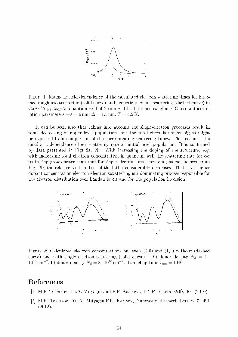
Figure 1: Magnetic eld dependence of the calculated electron scattering times for inter-face roughness scattering (solid curve) and acouctic phonons scattering (dashed curve) inGaAs/Al0.3Ga0.7As quantum well of 25 nm width. Interface roughness Gauss autocorre-lation parameters λ = 6 nm, ∆ = 1.5 nm, T = 4.2 K.
It can be seen also that taking into account the single-electron processes result insome decreasing of upper level population, but the total eect is not so big as mightbe expected from comparison of the corresponding scattering times. The reason is thequadratic dependence of e-e scattering rate on initial level population. It is conrmedby data presented in Figs 2a, 2b. With increasing the doping of the structure, e.g.with increasing total electron concentration in quantum well the scattering rate for e-escattering grows faster than that for single electron processes, and, as can be seen fromFig. 2b, the relative contribution of the latter considerably decreases. That is at higherdopant concentration electron-electron scxattering is a dominating process responsible forthe electron distribution over Landau levels and for the population inversion.
Figure 2: Calculated electron concentrations on levels (2,0) and (1,1) without (dashedcurve) and with single electron scattering (solid curve). а) donor density Nd = 1 ·1010 cm−2, b) donor density Nd = 8 · 1010 cm−2. Tunneling time τtun = 1 HC.
References
[1] M.P. Telenkov, Yu.A. Mityagin and P.F. Kartsev., JETP Letters 92(6), 401 (2010).
[2] M.P. Telenkov, Yu.A. Mityagin,P.F. Kartsev, Nanoscale Research Letters 7, 491(2012).
64

Exhibitors
65
Measuring electronic properties on the nanometer scale
K. Zwoli«ski
AM Technologies Polska Sp. z o. o.,Jerozolimskie Business Park,
Al. Jerozolimskie 146CTel: (+48 22) 532 28 05,[email protected],
www.amt.pl
Mapping materials physical properties such as impedance, capacitance, dielectric con-stants, dopant density, etc., at the nanoscale is of great interest to both materials andsemiconductor industries. With the invention of scanning tunneling microscopy (STM)and atomic force microscopy (AFM), a number of STM and AFM based techniques havebeen developed to probe materials properties. These include scanning near-eld to scan-ning microwave microscopy (SMM), scanning capacitance microscopy (SCM), scanningspreading resistance microscopy (SSRM), electrostatic force microscopy (EFM), current-sensing (or conductive) AFM (CSAFM), and Kelvin force microscopy (KFM). While eachmethod carries its own pros and cons, SMM and SCM have shown most promising poten-tials in this eld for both industrial applications and scientic research. Using microwavefrequency as the medium, SMM measures electromagnetic interactions of the microwavesignal from a sharp probe or aperture with the sample under test on a scale that issignicantly less than the wavelength of the radiation. This presentation is to give anintroduction to newest technologies used in scientic grade nanoinstruments from AgilentTechnologies.
66

Plasma processing equipment for DLC deposition for in-
frared optics
P. Chomiuk
APVACUUM Sp. z o.o.,ul. Klonowa 24, PL 62-002 Suchy Las, Poland
Diamond-like Carbon (DLC), due to its optical and mechanical properties, fullls highdemanding requirements for extreme applications like aviation or military. In this presen-tation a plasma-enhanced chemical vapor deposition (PECVD) system for DLC depositionis presented. A MicroSys 500 DLC equipment of MicroSystems GmbH, with parallel platealignment, provides deposition of a DLC lm with good homogeneity and good adhesionto substrate, that may be successfully utilised for infrared optics applications [1]. Infraredspectra of a Ge optic coated with DLC are shown in Fig. 1.
Figure 1:
References
[1] DLC Deposition for Infrared Optics (MicroSys 500), MicroSystems GmbH presenta-tion.
67

Nanoimprint Lithography a next generation high vol-
ume lithography technique for the transition of MEMS
technology to nanofabrication
R. Staudinger
EV Group Europe & Asia Pacic GmbHDI Erich Thallner Strasse 1
A - 4782 St. Florian /Inn [email protected]
www.EVGroup.com
EV Group (EVG) is a world leader in wafer-processing solutions for semiconductor,MEMS and nanotechnology applications. In addition to its dominant share of the marketfor wafer bonders, EVG holds a leading position in Nanoimprint Lithography (NIL) andlithography for advanced packaging and MEMS. With more than 15 years experience in allelds of imprint lithography (UV-NIL, micro contact printing and hot embossing), EVGis one of the leading experts focusing on various applications like optics, data storage,semiconductor, microTAS, microuidics, bioMEMS and many more, providing featuresizes ranging from macro down to the nano scale. EVG's extensive development eortsto deliver the promise of imprint lithography being a low cost, high resolution pattern-ing technique leaded to the breakthrough in 2010 getting structures of 12.5nm by usingEVG's low cost, multi use soft stamp technology. EVG strengthen its imprint lithographyposition by being not only an equipment supplier rather delivering total solutions withNILCom. EVG is a founder and leading partner in this consortium, consisting of imprintlithography supply chain companies and research organizations with the aim of providinga total solution path.
68

Wirebonding non-Si materials: the challenges of lasers,
emitters and detectors
J. Sedlmair
F&K Delvotec Semiconductor GmbHIndustriezeile 49a
A-5280 Braunau / Inn Austriawww.fkdelvotec.at
Wirebonding many high-performance devices can be dicult, not only because of thesmall lot sizes usually available. More troubling are often the compound semiconductorbase materials such as GaAs and InP which are notoriously less robust than Si. Focusingon practical aspects, the basic requirements of bonding such parts with Al or Au wires inball- or wedge-bonding processes will be discussed, followed by a sidelight on other wirematerials such as Pt, Cu and coated wires. Finally, some remarks will be made concerningthe proper way to characterize the bonds correctly by pull- and shear-tests.
69

3D Digital Microscope: HIROX KH-8700 full HD visual
inspection with 2D & 3D measurement `Easy, Fast, High
Quality'
E. Leonhardt
HIROX EUROPEMobile: +49 172 44 19 [email protected]
Hirox Co. Ltd. founded 1978 in Tokyo (Japan) as producer of high quality optics,invented the rst video microscope in 1985 and continues to develop the most innovativeoptics such as the Hirox 3D Rotary Head. We are leader in high-end 3D Digital Mi-croscopy, with thousands of systems sold worldwide to the R& D and QC departmentsfrom major industrial companies and universities in the eld of Micro Electronics, Semi-conductor, Chemistry, Automotive, Aerospace, Forensics, Museum. . .We are proud tocount the ITE Krakow, the Warsaw University of Technology, the PWPW Warsaw assome of our customers in Poland.
70

Modes of operation based on PeakForce Tapping tech-
nology in atomic force microscopes from Bruker
B. Radkowski
Labsoft Krzysztof Hermanul. Wantule 12, 02-828 Warszawa
Atomic Force Microscopy (AFM) is now widely used in the eld of characterization ofa variety of materials. In addition to the precise measurement of surface topography witha resolution enabling the observation of atomic steps, current devices of this type oera number of additional features, including the study of electrical, magnetic and thermalproperties. In this paper we present the latest technology in this eld, complementaryto already developed AFM techniques, which enhance the range of possible applications,including automated mode topographic imaging, mapping modes allowing evaluation ofsurface mechanical properties and electrical conductivity. Thanks to these innovations thearea of application of atomic force microscopy has been expanded signicantly, allowingtesting of materials that previously were not suitable for the use of such techniques. Thebasis of the latest modes of operation is a technique called PeakForce Tapping which isusing the lever oscillation with a frequency far below resonance, and in such way cancarry a surface scan during which each individual contact with the surface of the sampleis treated as an independent force spectroscopy experiment. Each contact of the tip withthe surface forms an individual force distance curve that is immediately analyzed usingthe unique software and electronics to enable realization of such measurements. In thisway, the most important factor associated with the implementation of this technique ofmeasurement the force of the contact between the tip and the surface of the sample is controlled in real-time.
71

When you need to see a new dimension Olympus pro-
vides the answer
N. Szyma«ski
Olympus Polska Sp. z o.o.ul. Suwak 3
02-676 WarszawaTel.: (48 22) 366 00 77
Mobile: +(48) 695 024 [email protected]
http://www.olympus-ims.com/en/microscope/opto-digital/
The Olympus DSX Series opto-digital microscopes combine advanced optics, electron-ics and know-how to create a scope so sophisticated it's simple. The result is incrediblyhigh-resolution visual images and versatile measurements backed by Olympus reliability.Thus, world-leading optics and leading-edge digital technology fuse into one easy-tousesystem that anyone can operate. Olympus, world leader in industrial microscopes, bringsobservation and analysis to a new dimension.
72
Uni - Export Instruments Polska
M. Fordon, A. Ginalski
Uni - Export Instruments Polskaul. Ludwika Kickiego 4a / 5004-369 Warsaw, POLANDtel.: +48 22 626 87 86
tel. / fax.: + 48 22 626 87 85e-mail: [email protected]
www.uni-export.com.pl
Technical support, service and sales of scientic and laboratory equipment:TESCAN/OXFORD INSTRUMENT/E2V SCIENTIFIC INSTRUMENTSScanning electron microscopes with tungsten heated cathode, eld emission, LaB6,
FIB system. Special software (lithography, image analysis), special stages and detectors(EDS, WDS, EBSD, EBIC, CL). Upgrade of older SEM and EDS systems.
AGILENT TECHNOLOGIES Vacuum Products DivisionVacuum pumps (rotary, scroll, turbomolecular, diusion and ion), complete pump-
ing systems (for high and ultrahigh vacuum), gauges for vacuum measurement, portable(mass-spec based) leak detection system, valves and vacuum accessories.
QUANTACHROME INSTRUMENTSInstruments for accurate, precise, and reliable characterization of powdered and porous
materials: adsorption and desorption isotherms, surface area measurement, pore sizedistribution, chemisorption studies, water sorption behavior, mercury porosimetry, trueand tapped density.
FORMULACTIONTURBISCAN, instruments dedicated to stability or instability analysis and to the
characterisation of concentrated emulsions, suspensions and foams. Detects nascent desta-bilization's phenomena (migration, change of the size of the particles) and the kinetics ofthese changes.
HORUS, instrument dedicated to lm formation analysis. From the kinetics of dryingor curing, displayed in real time, a wide range of information can be extracted such asobjective drying time.
ART MODERNE LABORTECHNIKHomogenizers based on `rotor-stator' construction dedicated for homogenization, emul-
sication, dispergation and disruption a wide range of dierent samples. SPECS - SurfaceNano Analysis
Customized UHV surface analysis systems. UHV equipment and components.Electron spectroscopy (XPS, UPS, AES, ISS). High resolution microscopes: LEEM,
SPM.
73