AND INSTALLATION, APPLICATION OF AUDIO FREQUENCY … · section i. ii. january, 1976...
131
Section I. II. January, 1976 C-76-250-1492-3 • r 0 \1 1- '1 iii SERVICE M~NUAL 5906 INSTALLATION, APPLICATION AND MAINTENANCE OF AUDIO FREQUENCY OVERLAY (AFO-II EQUIPMENT) * * * * * * * * * CONTENTS INTRODUCTION . . . . . . . . DESCRIPTION AND OPERATION. A. General . . . . . • • . . . 1. Track Circuit Operation . . . . 2. Equipment. . . . • . . . . . . . B. AFO-II Receiver . . . . . . 1. Receiver Board • . . . 2. Demodulator & Amplifier Board . c. Receiver Relay . . . . . . • • D. AFO-II Transmitter . . . . . . 1. Transmitter Boards • . . . . . 2. Modulator Board . . . • . • . . E. AFO-II Auxiliary Equipment . • . . 1. Track Coupling Units . . . 2. Blocking Reactor . . . • • Page 1/2 3 3 3 5 5 5 6 6 7 7 8 10 10 10 WESTINGHOUSE AIR ijRAKE COMPANY UNION SWITCH & SIGNAL DIVISION Swissvale Post Office,. Pittsburgh,. Pa. 15218 An American-Standard Company
Transcript of AND INSTALLATION, APPLICATION OF AUDIO FREQUENCY … · section i. ii. january, 1976...

Section
I.
II.
January, 1976 C-76-250-1492-3
•
r <~~~ 0 \1 1-'1 iii
SERVICE M~NUAL 5906
INSTALLATION, APPLICATION AND MAINTENANCE OF
AUDIO FREQUENCY OVERLAY (AFO-II EQUIPMENT)
* * * * * * * * *
CONTENTS
INTRODUCTION . . . . . . . . DESCRIPTION AND OPERATION.
A. General . . . . . • • . . . 1. Track Circuit Operation . . . . 2. Equipment. . . . • . . . . . . .
B. AFO-II Receiver . . . . . . 1. Receiver Board • . . . 2. Demodulator & Amplifier Board .
c. Receiver Relay . . . . . . • • D. AFO-II Transmitter . . . . . .
1. Transmitter Boards • . . . . . 2. Modulator Board . . . • . • . .
E. AFO-II Auxiliary Equipment . • . . 1. Track Coupling Units . . . 2. Blocking Reactor . . . • •
Page
1/2
3
3 3 5 5 5 6 6 7 7 8
10 10 10
WESTINGHOUSE AIR ijRAKE COMPANY UNION SWITCH & SIGNAL DIVISION Swissvale Post Office,. Pittsburgh,. Pa. 15218
An American-Standard Company

WABCD ~
CONTENTS
Section
III APPLICATION INFORMATION A·. Frequency Selection B. Receiver Relay c. Track Coupling Unit D. Blocking Reactor
Page
11 11 15 20 20 23
/' -k~ !:··, rfiKinr!}~Jrmf·cf~6~~ -~~p~lY,~ -~"" C· ., > ··:; ;•·2 4 ~- >'
IV.
v.
VI.
VII.
VIII VIII.
• __ ,.,ft .... 1. : ·i:J;ra,ck:: Terminal Protection '2. · Battery Line Protection
G. Surge-Ripple Filters
INSTALLATION .AND ADJUSTMENTS A •. Transmitter B. Receiver · c. Track Coupling Units D. Blocking Reactor E. Equipment Adjustments
FIELD INSPECTION AND SERVICE A. Field Test Equipment B. Periodic Inspection c. Track Units Field Servicing
1. Equipment Substitution Method 2. Voltage M.easurement Method
TROUBLE ANALYSIS TEST POINTS AND OSCILLOGRAMS A. General B. Field Applications c. Bench Testing D. Function Generator
PRINTED CIRCUIT BOARD CHECKOOT INSTRUCTIONS A. High Power Transmitte;r B. Low Power Transmitter c. Modulator Boards D. Receiver
PARTS LIST A. Complete. Unit. Part~ Lists B. Circuit Board Component Locations and
Parts Lists c. Hardware and Wiring
24 24 25
26 26 26 26 30 30
32 32 32 33 33 33
35 35 35 35 36
51 51 51 52 54
60 61
65 91
APPENDIX (IX) - UNIMODULE TYPE AFO-II EQUIPMENT {No Longer Manufactured)
9-1 Installation-& Adjustment 98 9-2 Field Inspection and Servicing 104 9-3 Printed Circuit Board Checkout Instr. 107 9-4 Parts List 115
,,.!.
ii
~--.

I. INTRODUCTION
The purpose of this pamphlet is to outline the principles of Audio Frequency Overlay (AFO-II) track circuits and to provide information to assist the user in applying AFO-II equipment.
This information is essential for planning AFO-II installation, and includes track circuit data necessary for laying out track circuits, along with frequency allocation rules for achieving the most efficient operation with the use of AFO-II equipment.
AFO-II. electronic track circuits provide fail-safe train detection which does not require insulated rail-joints, and can be used for highway crossing application or as continuous train detection in signal systems.
Availability of low and high power transmit_ters provides a flexible range of train detection.
The AFO-II signal is pulse modulated to provide a high degree of immunity to noise in the rails.
All AFO-II transmitters and receivers are completely transistorized and operate from a de power supply ranging from 8.8 to 16.2 volts(Normal 10,12, or 14 volt battery).
The following illustration shows a WABCO AFO-II Receiver. WABCO AFO-II transmitters, Receivers, and Track Coupling Units use the same size and style case (only the wiring differs). The case is constructed of sheet steel. Sections one through seven of this manual will describe these presently manufactured units; section eight covers AFO-II units which are no longer being manufactured but which may be operating on railroad property.
AN AFO-II RECEIVER UNIT (Sheet Steel Case Design)
5906, p. 1/2

-·

WABCO ~
II. DESCRIPTION AND OPERATION
A. General
Audio frequency overlay (AFO) equipment has been generated by the need for vital train detection: (a) in addition to that already present in a signaling system, and (b) which does not require insulated rail joints.
AFO-II equipment is designed to satisfy the above conditions using standard signaling power (8.8 to 16.2 VDC actual) and equipment.
The term "Audio Frequency" has been applied to this type' of equipment because it makes use of frequencies within the audio range (20-20,000 Hz).
1. Track Circuit Operation
An. AFO track circuit is composed of a transmitter receiver, and receiver relay. The transmitter and receiver require a de power supply for operation.
The transmitter introduces an audio signal of a specific assigned carrier ,frequency and moduiation rate into the track through two wires connected directly to the rails. The point at which the wires are connected defines one end of the positive track circuit.
The receiver, which only responds to a specific assigned carrier frequency and modulation rate, is also connected to the rails with two wires; this point defines the other end of the positive track circuit. Upon receiving the proper frequency, the receiver detects, amplifies, and rectifies the signal to provide an output to operate an external relay.
The contacts of the relay are then employed in the same fashion as conventional track relay contacts.
The AFO track circuit detects the presence of a train through loss of the audio frequency signal which is shunted by the train wheels. This is depricted in Figure 1. -- --·- ' - -----
A series of AFO-II track circuits, as shown in Section III, can be superimposed on a track section. Each track circuit will operate independently without interference from the operation of other AFO-II or de track circuits. This is particularly important where adjacent highway crossings have overlapping approach limits. Also, it allows an overlap at the crossing for an island circuit as shown in Figure 2.
5906; p. 3
•

WABCO ~
5906, p. 4
UNOCCUPIED TRACK CIRCUIT
DC POWER SOURCE
,\II IUlllll lllt, = = ;,um11111111111\~
RELAY
OCCUPIED TRACK CIRCUIT
DC POWER SOURCE
RECEIVER
l RELAY
CONTROLLED CIRCUITS
~ CONTROLLED CCIRCUITS
.._\llllllllttllltlllli-
~I I~ °',uu11111111111111~
ENERGIZED AFO SIGNAL SHUNTED DEENERGIZED
Figure 1. Typical AFO-ll Track Circuit Operation
J L TRACK
- -T I~ .... L,I I
AFO-Il (.'.) AFO-II TRANSMITTER AFO-lI z AFO-lI TRANSMITTER
#1 - #2 RECEIVER Vl RECEIVER Vl
#2 0 ,, ~
u I >- I TRACK ~ TRACK I RELAY (.'.) RELAY
#2 - #1 I
Figure 2. Typical AFO-ll Highway Crossing Layout With Overlapping Track Circuits

2. Equipment
All circuitry in the transmitter and receiver is ot printed circuit board construction. The P.C. boards
·are plug connected in a sheet steel housing designed for shelf/wall mounting, or rack mounting with A.A.R. terminal strips provided for circuit connections.
Surge protection is provided within the receiver and transmitter for both the de line and track iead inputs. See Section III-F for lightning protection requirements.
Reverse polarity protection is also included. If battery polarity accidentally reversed, a protective fuse will blow which disconnects the unit from the battery supply to prevent standby power loss and protect other equipment.
B. AFO~II Receiver
Because highway crossing control circuits are vital, the AFO-II receiver circuitry has been designed for fail-safe operation so. that a failure of any component or a drastic change in the values of components will reduce the power supplied to the receiver relay. Thus, the relay will not be energized due to equipment malfunction after proper installation and adjustment in accordance with Section IV of this Manual.
The receiver will operate over a de batte~y voltage range of 8.8 to 16.2 volts. In case of battery failure, the receiver will not be damaged from the battery charger rectifier, nor will the receiver relay be falsely energized. Extended operation directly from a rectifier is not recommended, since reliability will be reduced due to large ripple currents in filter capacitors.
A sensitivity adjustment is built into the receiver unit to obtain the proper shunting characteristics for each track circuit.
The AFO-II receiver is housed with all circuit components mounted on two printed circuit boards: Receiver, and Demodulator & Amplifier. Both boards are plug-connected within the housing and keyed to prevent improper insertion.
1. Receiver Board -N451054-40xx
The Receiver board contains two separate circuits, an amplifier and a relay driver. The AFO signals received from the rails are applied to the primary of the input transformer that is series tuned to the receiver frequency. Thus, it rejects low frequency ac and de which may be present in an existing track circuit. The output from the secondary is then amplified and filtered. A potentiometer adjusts the gain and, hence, the shunting sensitivity of the receiver. This signal is then applied to the input of a Demodulator & Amplifier board.
The output from the Demodulator & Amplifier board is then applied to the relay driver circuit on the receiver board, which is basically a power amplifier. The output from this circuit is then applied to the output transformer which is mounted on the Demodulator & Amplifier board.
_ 5_906 r p_~ 5

WABCC ~
2. Demodulator & Amplifier Board - N451054-4lxx
The Demodulator & Amplifier board is used in the AFO-II receiver for receiving modulated signals. It receives the input from the amplifier circuit on the Receiver board, demodulates it and provides additional amplification for external relay operation.
The signal from the Receiver board is applied to a demodulating circuit, ·and then to an L-C circuit tuned to the modulated frequency. The signal voltage developed across this circuit is then returned to the Receiver board where it is applied to the relay driver circuit. The output from the relay driver is then returned to the Demodulator & Amplifier board and applied to the primary of the output transformer. The output from this transformer is rectified and used to energize an external relay.
Receiver charactersitics are given in Table 1. See Section VII for J?arts Lis:t ..
TABLE 1. AFO-II RECEIVER CHARACTERISTICS
Input Voltage
Input Current
Output Voltage ( 400 ohm load)
Signal Sensitivity
Input Impedance (Track)
Output Load
Bandwidth
Operating Frequencies
Temperature Range
Surge Protection
C. Receiver Relay
8. 8 - 16. 2 VDC
O. 15 amp. at 12 VDC
6 VDC minimum (with 5 mV rms input signal and 8. 8 volts battery)
5 millivolts rms minimum detectable signal ( during on-time of modulation cycle)
1 ohm at center of assigned frequency (nominal)
400 or 500 ohm Relay ( PN150BH or DN22BH Relay, respectively)
-6 db at ±3. 0 % of as signed frequency
See Table 3
-40°C to +71 °C ( -40°F to+ 160°F)
Built-in
The receiver relay should be a WABCO DN-22BH (shelf) or PN-150BH (rack) relay. ·
See Section III-B for application characteristics.
5906, p. 6

WABCCI ~
D. AFO-II Transmitter
The AFO-II low power transmitter 100% and 30% output voltage taps. No transmitter is required or provided. is shown in Figure 4.
is designed with both other adjustment of the The range of each output
Selection of either a low or high power transmitter for any particular application is based on the required track circuit length, ballast reststance, frequency, etc. Either transmitter will operate on a de battery voltage range of 8.8 to 16.2 volts. The modulated signal provides noise immunity of the circuit and reduces battery consumption by the transmitter.
The AFO-II Transmitter contains four printed circuit boards which are plug-connected within the housing and are keyed to prevent improper insertion.
Transmitter characteristics are given in Table 2. See Section VIII for parts listing.
1. AFO-II TRANSMITTER BOARDS
B.
NOTE: * NOTE: **
The Transmitter Board {N451054-4901 to 4912 and 4925 to 4928**) consists of an audio oscillator stage, intermediate power amplifiers and the input transformer to the final. This hoard is used only on Low Power Units.
The Transmitter Board {N451054-4913 to 4924 and 4929 to 4932**) is basically similar to the aforementioned but has in addition a driver amplifier stage. This board is used only on High Power Transmitter Units.
The Output Transistors are mounted on the Transistor Board N451054~8601. This board is present in both Low and High Power Units.
Printed circuit board (N451043-5401 to 5416**) is the Low Power Transmitter Board. This board is used only on Low Power Transmitter Units and contains the fuse and filter for the input o.c. power source. Contained also on this board is the Push Pull output transformer and a series resonant L-C circuit which couples the signal from the push pull output transformer to the track. The secondary of the output transformer has a tap to provide 30% of the output voltage (or 10% output power) for short track circuits.
Last digit dependent upon modulating frequency. Last two digits are dependent upon the units operating frequency.
5906, p. 7

WAEICD ~
C2· Printed circuit board N451043-5501 to -5516**) is the High Power Transmitter Board. The High Power Transmitter board is used only on high power transmitter units. This board, with the exceptions of slight variations in component values and the absence of the 30% Voltage tap, is similar to that previously mentioned.
2. The Modulator Board N451054-3901 to -3908**) is used on both high and low Power Transmitters. The Modulator board contains an oscillator, an amplifier and a switching circuit. The oscillator output is applied to the amplifier, and then to the switching circuit which produces the assigned modulating signal for use on the Transmitter board.
The oscillator is tuned to the correct frequency at the factory and cannot be adjusted in the fie·ld.
Transmitter characteristics are given in Table 2. See Section VII for Parts Listing.
NOTE * Last digit dependent upon modulating frequency. NOTE ** Last two digits are dependent upon .the units
operating frequency.
5906, p. 8

. _;:1
· w~aca ~
TABLE 2. AFO-II TRANSMITTER CHARACTERISTICS
LOW POWER HIGH POWER
Input Voltage 8. 8 - 16. 2 VDC 8. 8 - 16. 2 VDC
Input Current:
100% Voltage 0.28 Amp. @12 V 1. 2 Amp. @12 V input output ( into 2 input ohm load)
30% Voltage O. 09 Amp. @12 V ( Not Applicable ) output ( into 2 input ohm load)
,.
Output Voltage 100% 1. 5 V rms during "ON" 3. O V rms during "ON" ( 2 ohm load, 12. O V period of mod. period of modulation battery) ( Modulator board re- . ( Modulator board removed)
moved)
Output Voltage 30% o. 445 V rms·during "ON" ( Not Applicable) ( alternate tap) period of mod.
( Modulator board re-moved)
Output Impedance 1 ohm . l ohm ( Nom. at center of assigned Freq. )
Operating Frequen- See Table 3 See Table 3 cies
Temp. Range -40°C to +71 °C -40°C to +71°0 ( -40°F to 160°F) ( -40°F to + l60°F)
Surge Protection Built-in Built-in
Min. Ballast 3 ohm/1000 Ft. 3 ohm/1000 Ft. Resistance
5906, p. 9

WABCCI ~
E. AFO-II i,\.uxiliary .Equ_ipment
1. Track. Coupling Units .. ' '
A coupling unit is used when the 'AFO· signal must be passed around insulated joints· and the existing track circuit energy must be blocked. This unit uses transformer coupling to pass the AFO signal to the next track section.in a fail-safe manner.· . . ..
Two coupling units are available: one for each CLASS of AFO-Il frequencies. Since each unit has tuned taps for each frequency in its class, one unit is required for each frequency to be passed around the insulated joints. ·
The frequency-determining taps are located inside the unit. The cover · can be secured with a locking wire once the proper connections have been made. .
The track coupling unit has the same dimensions and utilizes the same housing for, shelf/wall or rack mounting, as the receiver and transmitter.
Section VIII contains part.numbers references for the Track coupling units. Figure 15 (contained in Section IV) shows.typical wiring arrangements for track coupling units •
5906, p. 10
. . 2. Blocking Reactor
The purpose of the blocking reactor is to block the AFO signal while passing de and low frequency ac.
A reactor recommended for this application is blocking reactor, N451036-0302, which bas a de resistance of O. 01 ohm and a current rating. of 7 amperes. This reactor may be mounted on a relay rack in a PN-250 space or on a wall or shelf. Dimensions are 8'' x 5" mounting plate with a depth of 3-5/8".
See "Blocking Reactor" Section ill-D for various applications to AFO-II track circuits.
..

ill. APPLICATION INFORMATION
A. Frequency Selection .. ·
The AFO-II system provides low and high power transmitter and receiver units in sixteen different frequencies. The sixteen· different frequencies shown in Table 3 are divided into two groups of eight each: Class 1,. ~ Cla~s 2 •. Corresponqtng · frequencies in e~c~ class use the same mqdu.Iation rate. , ·
Class 1 frequencies are intended for use in single track areas and for the first track of a double track area.
. -Class 2 frequencies are used on the second track of a double track area. J. '~
If more than two parallel tracks are involved, the frequency classes must be alternated with respect to adjacent tracks to reduce the possibility of inductance coupling between tracks. ·
' ·:
AFO-II frequencies have been computer selected within each Class to:
...
1. ·obtain optimum separation from the.sum. and difference frequencies of ai;;signed AFO-II frequencies.
2. A void harmonics up to the fifth harmonic of AFO-II frequencies.
3. Minimize harmonic mixing and the mixing of harmonics with the assigned AFO-II frequencies.
4. Obtain optimum separation from the 60 cycle power frequency and its harmonics and the mixing of these with AFO-II frequencies.
TABLE 3. AFO-II FREQUENCIES
FREQUENCY , , CLASS 1 CLASS 2 MODULATION DESIGNATION FREQUENCY FREQUENCY RATE
', ' Fl 885 Hz 930 Hz 18 Hz F2 1050 Hz 1120 Hz 22 Hz
· F3 1330 Hz 1420 Hz 27 Hz F4 1860 Hz 2,140 Hz 39 Hz· F5 2540 Hz • 2720'Hz 49 Hz F6 ·· 3360 Hz i
3410 Hz 68 Hz
NOTE: The two AFO-II track coupling units are tuned only for those frequencies shown above and cannot be ...
used with frequencies shown below.
F7 4565 Hz 5090 Hz 94 Hz F8 6180 Hz 6330 Hz 139 Hz
5906, p. 11

WABCD ~
Frequencies not compatible with the AFO-II track coupling units, as indicated in Table 3, must be applied in a track section where it is not necessary to bypass an insulated joint.
Certain basic rules must be followed in the application of AFO-II track circuit equipment to ensure maximum effectiveness and security and are listed under "Application Rules".
APPLICATION RULES
1. Do not repeat the same frequency on the same track unless the track circuits are separated by two pairs of insulated joints.
a) If a coupling unit is used to bypass a set of insulated joints, these joints may not be counted in applying Rule 1 above.
2. Do. pot mix frequencies from both classes on one track. However, after exhausting the frequencies of one class, the other class may be used on the same track when one pair of insulated joints separates the two classes.
3. The same AFO-Il frequency must not be located adjacent on parallel tracks, frequencies must be staggered.
4. Select frequencies for track circuits on the same track in the following orders.
Class 1: Fl, F4, F6, F3, F5, F2, F7, F8 Class 2: F2, F5, F3, F4, F6, Fl, F8, F7
Frequencies F7 and F8 may be used at random with other frequencies within their class. Adjacent track circuits, on adjacent parallel tracks, should be assigned from different classes and be paired as shown above and in Figure 3. For example: F6 of Class 1 would be next to F3 of Class 2.
5. When more than one highway crossing is involved in an AFO layout, a ripple-free power supply must be provided for the transmitters. Surge-ripple filters N451036-0701 for low power and N451036-0702 for high power, are available for insertion between the ·transmitter and the power supply. See Paragraph "E" "Track Leads and Power Supply".
5906, p. 12
-"-

,--.. ,
'TRACK NO. 1 CLASS 1 FREQ.
TRACK NO. 2 CLASS 2 FREQ.
T-Fl
--T-F2
-
MULTIPLE HIGJiWAY ¢ROSSINGS ... ,
1 ... ,
' R-F4 R-Fl T-F4 T-F6 R""F3 R-F6 T-F3 T-F5
- -- - ' -. - -- -R-F5 R-F2 T-F5 T-F3: R-F4 R-F3 T-F4 T-F6
- . - -- - - - ---,, ''
T = AF0-11 TRANSMITTER R = AF0-11 RECEIVER . F = FREQUENCY DESIGNATION (PER TABLE 3)
... , R-F2 R-F5
R-Fl R-F6
-,,
Figure 3. Typical Track Circuit Frequency Layout for Parallel Tracks
T-F2
--T-Fl
--
In selecting and applyi,ng the frequencies, the required length of the track circuit must also be considered, since the AFO signal attenuation in the track circuit is directly proportional to _the frequency.
Curve A in Figure 4 shows the maximum effective length versus frequency when using a low power transmitter.
Short track circuits, down to 100 feet in length, can be achieved with the low power transmitter by connecting the track 16-ads to terminals B4 and D3 for 30% output voltage. For maximum range, use terminals A3 and D3 which provides 100% output voltage.
When the required track circuit length exceeds the range of the low power transmitter for the selected frequency, U:se a high power transmitter.
NOTE
For each coupling unit used in an AFO-II track circuit, the effective length of that track circuit is reduced by 500 feet.
It should be noted that Figure 4 represents the maximum lengths for adjusting the track circuit at 20 ohms ballast resistance and does not consider the increase in receding ringing distance resulting from a drop in ballast resistance. The use of this chart in conjunction with ·Figures 5, 6, 7, and 8 is recommended.
After selecting the frequenc~es and determining the requirements of low and high power transmitters,· the recei vers:j/ and transmi tters,r may be ordered from the "Parts List" in Section VII'.
5906, p. 13

WABCD ~
"' .... 0:: w J:
z >-u z w ::> 0 w 0:: u..
5906, p. 14
6500
6000
5500
5000
4500
4000
3500
3000
2500
2,000
1500
1000
2
M~IMUM T~CK.CIRCUIT LENGTH WITH LOW POWER TRANSMITTER TO OBTAIN 5mV AT THE RECEIVER WITH 0,060 SHUNT
·. AND 200 PER rooo FT. BALLAST~ 'l=OR .. LONGER LENGTH CIRCUITS USE HIGH POWER TRANSMITTERS.
A - 100% OUTPUT
B - 30% OUTPUT VOLTAGE
6 • TRACK CIRCUIT LENGTH IN THOUSA!s!O FEET
Figure 4. Low Power Transmitter Range

WABCD -~-
B. · Receiver Relay
In order to utilize the optimum shunting characteristics of the AFO-II equip-: ment, the use of the WABCO DN-22BH or PN-150BH relay is recommended. These relays have a high release-to-working voltage ratio which results in closer toler'"" ance between the shunting and pick-up values of the track circuit.
This feature is especially significant when considering the "receding ringing" distance. This_ is the distance by which a train must be beyond. the x:eceiver track connection ( when leaving the AFO track circuit) in· order for the receiver relay to pick up. This distance should be as short as possible for the best utilization of the track circuit.
Other 400 to 500 ohm_ relays can be used with AFO-II, but longer receding ringing distances will result. See Figures 5, 6, 7, and 8; and compare the "Receding Ringing Distance in Feet" versus "Track Circuit Length" ·for the effect that ballast resistance and type of relay have on the receding ringing distance. Also, compare the difference in receding ringing distance for each frequency -885 Hz; 1050 Hz, 1860 Hz, and 3410 Hz.
Each set of curves is based on:
1. Setting the receiver sensitivity with INFINITE BALLAST RESISTANCE using att O. 06 OHM RESISTIVE TRACK SHUNT at the receiver connections; and
2. Checking the receding ringing dfstance with a ZERO OHM SHUNT at the _BALLAST RESISTANCE INDICATED on the curve.
These parameters are valid since {a) the AFO circuit must always be adjusted with an 0.06 ohm shunt at the best obtainable ballast condition and {b) the actual ballast resistance will be changing randomly with variations in weather conditions:
The curves indicate the following:
1. Lower frequencies inherently have a longer receding ringing distance than the higher frequencies.
2. Optimum ballast condition will result in the shortest receding ringing distance for the frequency and length of track circuit.
3. The type of relay used with the receiver is an important factor affecting "receding ringing" distance.
5906, p. 15

WRBCD ~
150
I-w ..... u.
£ w u z <( I-V'l
a 0 z 100 <5 z ~
0 £ a w u w 0::
50
0
5906, p. 16
FREQUENCY 885 Hz
I CURVE A - STYLE PN-150BH RELAY
CURVE B - STYLE DN-11, 4 POINT
CURVE C - STYLE PN-1508
2
A
A
3
TRACK CIRCUIT LENGTH IN THOUSAND FEET
4
Figure 5. 885 Hz Receding Ringing Distances
MINIMUM BALLAST IN OHMS PER THOUSAND FEET
3 ohms
5 ohms
10 ohms
20 ohms

150
I-w w u.. z w v z <( I-v,
0
0 z 0 z 100 o1 0 z 0 w v w
"' ,'
0
FREQUENCY - 1050 Hz I .
CURVE A - STYLE PN-1508H RELAY
CURVE B - STYLE DN-11, 4 .POINT
CURVE C - STYLE PN-1508
2 3
TRACK CIRCUIT LENGTH IN THOUSAND FEET
,·
4
MINIMUM BALLAST IN OHMS
3 ohms
5 ohms
10 ohms
Figure 6. 1050 Hz Receding R~ing Distances
WABCO -~-
~·-,,
5906, p. 17

WABCC ~
5906, p. 18
150
.... w w IJ..
z w u z -<( .... v,
0
0 z (!)
100 z ;;;?
0 z 0 w u w c,:
0
·---. -~ .... •.,_Oo,•·-~.,..,,....._ ........... ,..Q., ... ~·::--":#'_.,,_ ....... ~ .... '·--- ---- -· - ···-
FREOUENCY-'.1860-Hz · I - • ·, '
. <>-, /;.
CURVE A - STYLE" PN-150BH,RELAY
CURVE B - STYLE bN-11, 4 POINT RELAY
ClJR'v'E C - STYLE P~-f50B RELAY ~ .\ '· ; . ,,.-·---·-·-- --...... --...
'· , \
'-\
\
' "\
\ "\
"-~,
. !
1 ! p:_
3 ohms
3
TRACK CIRCUIT LENGTH IN THOUSAND FEET
4
MINIMUM ___ JIA.LLAST,J N
OHMS
3 ohms
\)
5 ohms
JO ohms
20 ohms

}-w w u. z w u z -<{ }-V)
Cl
0 z (5 z a::
0 z Cl w u w a::
I FREQUENCY - 3410 Hz
I CURVE A - STYLE PN-150BH RELAY
CURVE B - STYLE DN-11, 4 POINT RELAY
CURVE C - STYLE PN-1508 RELAY
3 ohms
3 ohms MINIMUM BALLAST IN OHMS
1501--~~~~~1--~~~~--lf--~~---+~-+1~~~~~-l-~~~~~-1
3 ohms
100
5 ohms
50
10 ohms
20 ohms
0 2 3 4
TRACK CIRCUIT LENGTH IN THOUSAND FEET
Figure 8. 3410 Hz Receding Ringing Distances
WABCC ~-
5906, p. 19

WABCD ~
C. Track Coupling Units
The AFO-II track coupling unit is used for passing the AFO signal around a pair of insulated rail joints, while blocking de or other frequency ac used on the same track section. There are two track coupling units to readily pass any one of the six frequencies in the class for which it is· tuned and connected, and reject all other frequencies. See Table 3.
NOTE
Since each unit has tuned internal taps for each frequency in its class, one unit is required for each frequency to be passed around the insulated joint pair.
Each time an AFO-II signal is coupled around insulated joints, the effective length of the AFO track circuit is reduced by 500 feet.
Due to severe restriction of effective track circuit lengths couplin~ units cannot be used to bypass ~he followinq AFO-II frequencies. 4565, 5090, 6180, 6330Hz. see figure 15 for wiring connections and Part No. References. -
D. Blocking Reactor
In some applications a blocking reactor must be installed in series with one lead of an existing de battery rail connection which occurs near an AFO-Il track circuit to prevent shunting the AFO signal through the battery.
The purpose of the reactor is to block the AFO signal while passing de and. low frequency ac. See View "A", Figure 10.
This is not necessary if an AFO-II track circuit occurs near the relay end of an existing de track circuit. The coils in the relay will provide the necessary impedance to block the AFO signal.
The need for the reactor depends upon the impedance presented by the existing de equipment, their leads, their distance from the AFO-Il track circuit, and the AFO-II frequency employed. One reactor is effective for all AFO frequencies. Figure 9 shows the relationship between minimum impedance, AFO-Il frequency, and distance. For example, if the AFO frequency is 1330 Hz and the distance is 200 feet, a reactor must be installed if the impedance in path A. B, C, and D is less than O. 7 ohm.
Blocking reactors may also be used for applications as shown in views "B" to "D", Figure 10.
View "B" - Allows the de track circuit to be shunted by a switch circuit controller without shunting the AFO signal.
View "C" - Defines the AFO track circuit at a specific point with insulated joints and allows the de circuit to pass.
View "D" - Keeps the AFO signal out of the fouling circuit at a turnout.
5906, p. 20 1

w u z <:( 1.0 0 ~ ~
0.5
0
MINUMUM REQUIRED IMPEDANCE IN OHMS OF CIRCUIT A-8-C-D .
TO APPROXIMATE EXISTING IMPEDANCE, ADD RESISTANCE OF A-8- AND C-0.
l .... •--d--•!Ooll A AFO-+- TRACK
TRANSMITTER C OR RECEIVER
TRACK BATTERY.
DISTANCE "d11 IN FEET .
fl = 885 Hz f2 = 930 Hz f3 = 1050 Hz f4 = 1120 Hz f5 = 1330 Hz f6 = 1420 Hz fl = 1860 Hz f8 = 2140 Hz f9 = 2540 Hz f10 = 2720 Hz f11 . = 3360 Hz f12 = 3410 Hz f13 = 4565 Hz f14 = 5090 Hz f15 = 6180 Hz f16 = 6330 Hz
Figure 9. Requirements for Blo.cking Reactor
600
5906, p. 21

WABCO ~
y: DC BATTERY
AFO AND DC-
REACTOR
AFO AND DC
AFO AND DC
2
DC ONLY
REACTOR
1+ j
j
j'" I 2.
AFO AND DC~
REACTOR
VIEW "A"
VIEW "B"
TRACK OR
VIEW "C"
REACTOR
VIEW "D"
AFO-II
TRANSMITTER
AFO AND DC
OR RECEIVER
TRACK
TRACK
DC TRACK ONLY
REACTOR
AFO AND DC
DC ONLY
TRACK
Figure 10. Applications of Reactor to AFO-Il Track Circuits
5906, p. 22

E. Track Leads and Power Supply
Leads from the AFO-II units to the track should be arranged to minimize their series inductance. Unsheathed single wires may be used in pairs, provided that they are twistea,·or kepi together within the same conduit. Metal-sheathed .. siiigle wties may not be used. Sheathed wire or conduit is not required for AFO-II wiring within the wayside housing. A transmitter and receiver unit of the aame frequency should have its own leads to the track •.
It is recommended that the battery charger rectifier leads be wired directly to the battery and then to the power busses or equipment. This will prevent the battery from being removed from the circuit due to a broken wire and will ensure a ripple-free power supply.
A resistor should never be placed in the power lead to a transmitter or receiver, since the total power lead resistance should be less than o. 15 ohm for transmitters and o. 5 ohm for receivers. If either of these values is exceeded, or if a ·signal ( or ripple) greater than O. 5 volt peak-to-peak exists on the power leads, a surge-ripple filter must be employed.
The following total lead wire resistances are the maximum permissible for maximum track circuit length and minimum receding ringing. distance:
1. Transmitter to Rails
2. Receiver to Rails
3. Receiver to Relay
4~ Battery to Receiver
5. Battery to Transmitter
F. Lightning Protection
0.15 ohm
0.15 ohm
25. 00 ohms
0. 5 ohm
0.15 ohm
Particular attention must be given to lightning protection during installation.
In order to limit the surge voltages, it .is necessary to employ suitable arresters between any points of exposure. The simplest way is to use a shunt arrester between the track leads to each unit and series arresters from each track lead to a common ground bus. This common ground bus should also be connected directly to the housings, signal poles, and all grounds at the location to limit the surge voltage between any connections on equipment or between equipment and housing.
NOTE Ground wires should be short and without sharp bends.
~abh of the series arresters should limit the surge voltage across itself to less thru;i 1500 volts (peak) in order to preve~t the voltage between any two points exceeding 3000 volts (peak).
Lightning damage can occur from surges entering the AFO-Il units either through the track terminals or through the battery terminals. These terminals must be protected as follows:
W~EJCD. · ~
5906, p. 23

WAS CC ~
1. Track Terminal Protection
The Track terminals of each AFO-Il transmitter and receiver should be protected by both series and shunt lightning arresters as shown in Figure 11.
Reference 1 should be a WABCO USG Series Arrester. This arrester has a minimum breakdown rating of 500 peak volts and a maxi.mum rating of 1200 peak volts.
Reference 2 should be a WABCO USG Shunt Arrester. This arrester has a minimum breakdown rating of 50 peak volts and a maximum rating of 300 peak volts.
Ground connections, reference 3, should be made to the ~ommon low voltage ground bus system that includes grounds at cases or houses. Make ground connections and jumpers with #6 AWG or larger wire. Messenger wire or metallic sheath ~f ,~able, if used,may serve as tie-in between cases or houses.
AFO-ll TRANSMITTER
0
TRACK
3
AFO-ll RECEIVER
0
3
N314265, USG SHUNT ARRESTER ~ GROUND BUS ,'\ N327989 USG SERIES ARRESTER (WITH TERM. BLOCK _/i....Ji"""~__;;..;:;..;;._;;_.;;..:;...1-..::..:::....:;:..-=.:=-=.;:::.:::::.:::....-=:=:=-=-=-===--=-:..:..:~:.......::::=.:~_!.._.:=~=.:.L.-~~~~--'
5906, p. 24
Figure 11. Track Lead Lightning Protection
2. Battery Line Protection
The AFO-Il transmitters and receivers, although they have built-in surge suppresion, will require additional protection across the power supply. This is accomplished by using USG Shunt Arrester, reference 2, across the power leads to the AFO-II equipment as illustrated in Figure 12.

+
DC POWER BUSS
AF0-8
.c ::: 0 AFO-N } TO AFO-lI UNITS
(2) N314266, USG SHUNT ARRESTER (WITH TEAM BLOCK)
Figure 12. Power Supply Lightning Protection
G. Surge-Ripple Filters
Normal operation of AFO-Il transmitters and receivers directly from a rectifier is not recommended since reliability of filter components will decrease due to excessive ripple. If the battery supply has a ripple or an ac signal greater than O. 5V peak-to-peak, a surge-ripple filter must be used. If more than one filter is required because of current capacity, it is _!'~commended that all transmitters be connected to one filter and all r~ceivers be connected to another filter.
WABCD -~
A·transmitter and receiver of the same frequency should not be connected to the same surge-ripple filter;_ nor should they be connected to the same battery · unless a surge-ripple filter is employed to isolate their power leads. This requirement is satisfied by placing a surge-ripple filter in the power leads to either unit, but_preferably the receiver. When more than one transmitter/receiver pair is powered from the same source, connecting all the receivers to one filter ( up to the filter's current capacity) will satisfy the requirement.
See_ Parts List in Section VIII for surge-ripple filter part numbers.
5906, p. 25

WAEICD ~
IV. INSTALLATION AND ADJUSTMENTS
All AFO-II equipment must be installed in accordance with approved application plans. · ···- -~-< · · -
Leave de power for·. all:· AFO-II equipmentp·«iscon:nected until initial equipment adjustments are to be made as outlined under "Equipment Adjustments". Paragraph "E"·.
A. Transmitter (Re_~er to Figure- 13)';· . ·' I . ,•
~ , ' • ,t~. -~ ... :
Although each transmitter is equipped with six A.A.R. terminals only four are used for both low power and high power transmitter connections.1 -~ . , . · ,
1. -Connect the positive and negative power supply to terminal #1 and #2 respectively. Observe correct polarity. (+DC i ~,.-DC f 2).
2. Connect the track leads to terminals #3 and #4. This. connection provides 100% output voltage as needed for longer circuits. For shorter circuits (Less ·th~n 300 ft.) connect the track leads to terminals 4 & 5. This connection provides a ·30% output volt'age and is sufficient to oper~te the shorter circuit while ,saving. on pow:er. . '
B. Receiver (Refer to Figure 13)
All six terminals are used for receiver connections.
1. Connect the positive and negative power supply to terminals #;t and #2 ,. respectively. ''Observe correct polarity. {+DC #1, -DC # 2).
2. Connect the track leads to terminalS#3 and #4.
3. Connect the+ and - relay leads to.receiver terminals #5 and #6, respectively. Observe correct polarity.
c. Track Coupling Units
A track coupling unit is used when the AFO signal must be passed around insulated joints and the existing track circuit energy must be clocked. See Figure 14.
The track coupling unit selection, Class 1 or Class 2, is based on the class of the frequency for which it is used.
Total track lead resistance should be kept below 0.15 ohms per pair. Coupling units should not be used within 100 feet of a receiver or transmitter.
5906, p. 26

u, I.O 0
°' -.... 10 ·• ,-N '3
TRACK
BATTERY POSITIVE
BATTERY NEGATIVE
AF0-11 TRANSMITTER
ARRESTERS
er: w
~ Q.
~ ..J
' ' ' er:', ~I 01 a. I a, i: I
I
l
3~~~- ___ .J ~
BAn:ERY POSITIVE
BATTERY NEGATIVE
AF0-11 RECEIVER
* Only one qr the other Lead is required.
Figure 13. TYPICAL WIRE CONNECTIONS FOR TRANSMITTER AND RECEIVER
ARRESTERS
TRACK RELAY
-~\I "~:n , , .. a

wAaca ~
LARRESTERS .J
Figure 14. Track Coupling Unit Application
NOTE
Since each unit has tuned internal taps for each frequency in its class, one unit is required for each frequency to be passed around the insulated joint. See Table 4.
Reference Figure 15.
1. Connect track leads from terminals # 3 and # 4 t.o the rails on the transmitter side of the insulated joints.
2. Connect track leads from terminals.#! and #2t.o the rails on the receiver side of the insulated joints.
·within the housing cover there are four wires on terminal strips which must be properly connected to assign the desired frequency. See Table 4 and Figure 15.
3. Connect the BLACK and BROWN wires to one of the assigned frequencies as indicated on terminals one to eight.
4. Connect the SLATE and BLUE wires only when one of the first three frequencies are assigned. When not assigned, the slate and blue wires should be connected to one of the spare terminals ( 4 or 5 ).
s. The LEAD PROTECTION portion of Figure 15 shows the proper arrangement of serie.s and shunt arresters to be used in conjunction with its coupling unit.
5906, p. 28

WAIIIC.a ~
TABLE:· .4. INTERNAL .TERMI?-11lli .. BOARD CONNECTIONS
CONNECT FREQUENCY (HZ) WIRE· (COLOR) ON TERMINAL
CLASS 1
885 1050 1330 1860 2540 3360
CLASS 2 BLACK BROWN SLATE BLUE
· (Left Side): {Right Side) (Left Side) (Right Side)* 930 1 1 1 1
1120 2 2 2 2 1420 3 3 3 3 2140 6 6 SPARE ·sPARE 2720 7 7 SPARE SPARE 3410 8 8 SPARE SPARE
* Indicates terminal strip on left or right side of circuit board as seen from the front.
TO{ TRM:k
LEAD PROTEC.TION
_rRECOMM'E.filJ)EX,TRAC.IIC L,E411D Pllarl!.C'T10:-
' Z COUPLING 3 /
(!) \ ""'" .( (!) I HZ .4 \
(!)N314ZG,s.u.se, s..iu ... T AA.Rtntst @NSZ7989,05G S!.Rlt!.5 WITH. TE.Cltvt."BLOCK.
CIRCUIT SYMBOL
Cl.ASS & COUPLIMli UlltT
}TO TRACK
Figure 15. Typical Wire Connections.for Track e~uplilMJ Units
5906, p. 29

WABCO ~
D. Blocking Reactor ( Refer to Figure 10)
Connect blocking react.or in series with one side of a circuit or track lead according to application requirements using terminals 1 and 2. See ''Blocking. -Reactor" under "AFO-II Auxiliary Units" and Figure 10 for various applications to AFO-II track circuits. • ·_ 1, ,.
E. Equipment Adjustments
After ALL TRACK CIRCUIT EQUIPMENT HAS BEEN CONNECTED, initial adjustments must be made using the following outlined procedures:
1. Using a vo~tmeter, check the de supply that will be used at the trans-mitter and receiver for correct voltage (8.8 .- 16.2 volts) .
. 2. Connect the de power to all AFO-II equipment.
NOTE
The equipment will not be damaged if de power is applied with the wrong polarity, but the internal protective fuses will be blown and must be replaced before further operation.
3. Connect a de voltmeter ( should have at least a 10, 000 ohms/volt sensitivity and a 0-10 volt range) across the relay terminals.
4. When power is applied, a de voltage of at least 6 volts should be devel-. oped across the receiver relay terminals. If the relay does not pick up, loosen the lock nut on the sensitivity adjustment and turn the shaft clockwise until the relay picks up. Then lightly tighten the lock nut.
NOTE
If the relay fails to energize, check all connections on transmitter, receiver, track coupling units , and reactors.
If the track circuit length is over 1500 ft. for F7 and F8 or 2500 ft. for Fl through F6 ( See Table 3), it may be necessary to use a high power · transmitter.
5. Connect a O. 06 ohm resistance shunt across the rails at the receiver track connections using rail clamps to insure good contact.
5906, p. 30

NOTE
In no case should the receiver be adjusted for · a shunt of less than O. 06 ohm resistance.
_,... .......... ~ti
'~~
If a higher resistance shunt is used, the overlap distance will be increased proportionately. It is not necessary to check the shunting at the transmitter, since it will be the same.
IMPORTANT
This adjustment should be made when the ballast is in good condition ( 20 ohms or higher per one thousand feet). This will avoid any appreciable decrease in shunting sensitivity with any further improvement in ballast. Also, all batteries must be fully charged and ALL track equipment connected.
6. Loosen the receiver sensitivity adjustment lock nut and adjust the receiver sensitivity so that the relay just drops out with the shunt in place. Observe and record the voltmeter reading.
7. Tighten the sensitivity adjustment_ lock nut and check the voltmeter to see that tightening the lock nut has not changed the voltmeter reading. If necessary, loosen the nut, readjust the sensitivity and tighten the nut again.
8. Remove the track shunt. The relay should then pick up.
NOTE
After replacing a transmitter or receiver, or any printed circuit board, the circuit must be readjusted.
Multiple receivers are frequently used to provide several track circuits with one transmitter. The shunting of each receiver must be adjusted individually. Adjustment of one receiver will not appreciably affect the adjustment of another receiver.
5906, p. 31 /

WABCD ~
V. FIELD INSPECTION AND SERVICING
This section contains the information necessary for routine inspection and determining the causes of failure or faulty operation of the equipment in the field. Repairs to transmitters, receivers ·and.other components should not be attempted in the field. A defective qnit or printed circuit board should be replaced and repaired. . .
AFO-Il troubleshooting niay be accomplished in two ways. The maintainer may take test equipment with him to make input and output voltage measurements of the AFO receivers and transmitters. Or, he may carry a spare transmitter and receiver which are in good working order, and substitute these in turn for each unit of an installation, until the faulty unit is found. The use of complete units for the substitution method of troubleshooting is preferable. Alternatively, malfunctions may be isolated to a particular printed circuit board by substituting spare boards in each unit until the faulty board is found.
NOTE
If, during field servicing, it is necessary to replace a transmitter, a receiver unit, a printed circuit board, or a receiver relay to correct a malfunction, the circuit should be re-adjusted in accordance with procedures given in Section IV of this service man.ual.
A. Field Te.st Equipment
A basic requirement for AFO-II field inspection and maintenance \lllder either plan noted above is a de voltmeter for checking the battery supply voltage. Where an extra transmitter and receiver of the proper frequency may be taken to the installation requiring maintenance, no other test equipment will be needed. Where an extra transmitter and receiver are not available, use a multimeter with a 5000 ohms per volt minimum input impedance, a 0-2. 5 volts rms ac range and a 0-50 VDC range.
B. Periodic Inspection
The inspections shown below are all that are required, and may be performed. on whatever schedule the customer deems necessary.
1. Visually inspect the units for the condition of the cases, terminals and wiring.
2. Check the lightning arresters to determine whether they are in. good operating condition.
3. Using a de voltmeter, check the battery voltage for 8. 8 to 16. 2 volts.
5906, 1?• 32

4. Shunt the track circuit and dleck the control relay voltage ·witH1a de~ voltmeter and compare it with the last recorded :reading.- ,. ··
C. Track Units Field Servicing
1. Equipment Substitution Method . .- : /... ~ .. ·: ; · r ,·r ·.• · . ;
Where a spare transmitter and receiver of the correct. frequency are available, the following method may be used to determine the ca.use of failure or improper operation of an AFO track circuit installation. · ·
a. Using a de voltmeter, check the battery for a reading of 8. 8 to 16. 2 volts. ·
b. Examine the receiver sensitivity adjustment lock nut to determine that the potentiometer adjustment is locked tight.
c. Substitute a spare transmitter for the original transmitter and check for correct operation. If operation is not correct, proceed to step d. below.
d. Substitute a spare receiver for the original receiver , and check the correct operation. If operation is now correct, reconnect the original transmitter and check for correct operation (both receiver and transmitter could be defective). Re-adjust the track circuit.
e. If neither the battery nor the transmitter or receiver are at fault, check the track bootleg connections, and the AFO relay. A defective track coupling unit, where one is used, may be a cause of the.difficulty. Check all terminals used in the coupling unit to ensure proper connection. See Section IV, C, for typical wiring connections in coupling unit.
2. Voltage Measurement-Method
As an alternative to the foregoing, the receiver and the transmitter output voltages may be measured to determine the condition of these units. Proceed as follows:
a. Using a de voltmeter, check the battery voltage for 8. 8 to 16. 2 volts.
Using the de voltmeter, measure the receiver output voltage at terminals #5 and #6 for a value equal to the pickup voltage of the AFO relay, or higher. If this voltage is at the pickup voltage or above, the difficulty will be in the AFO relay or the wiring between the unit and the relay.
c. If the voltmeter reading at #5 and ,t.6 shows low voltage or no voltage, recheck the track circuit adjustment as outlined in Section IV.
59,06, .P• 33.

WAaca• ~
d. If the receiver output voltage<.i¬ secured by·per:forming•.tbe? above clleck, disconneet the· transmitter .f:t:om the t:nack,eircuitJ Then, with a L 5 ohm load resistor across the transmitter output terminals, measure the transmitter output voltage"·QSing0 rur ac '· .. · ... , ' voltmeter. The reading should be o. 9 volt or higher for the.low . power transmitter and 1. 4 volts OF liigher for ,the·high power ,: transmitter. If the voltage is less than these" values, the "transmit-
r. '..:
' ter requires repair and should· be repl abed b;n another· :unit.' " ' ·
•·1
If neither the receiver nor transmitter. is fa:ulty;· the·problem :rnayL · ;..;.; , be in the track leads or connections, or. in tlie rail bond,oonnections_. ··
1,:,.
,i•'
""·::· .!.
'I , .
.:,·· k
~.·~ ..
u
-~ -,~ : .: ..
'·
'·
.. ~ . \
f.
,.i.
·. :L.; ~ ('
......... ~-.~!'..
.5906, p. 34
1, I .1

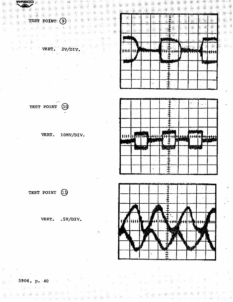
VI TROUBLE ANALYSIS TEST POINTS ANO OSCILLOGRAMS
A. GENERAL
WABCD ~
Figure 16 provides oscillograms which represent the typical waveforms and voltage levels present at various points within the AFO-II Transmitter/Receiver circuitry. Each oscillogram is presented with reference to a particular test point(s). Figures 17 and 18 show the physical location of the various test points while Figures 19 and 20 show the test point(s) schematic locations.
NOTE
The oscillograms_ are used to represent typical waveforms and voltages that can be found in AFO II equipment. Small variations of waveforms and voltages may be present on the p~~ticular unit being tested.
Service of the AFO II equipment should not be attempted by unqualified personnel. Personnel assigned to service AFO II equipment should have had previous experience with the type circuitry found in AFO II equipment. In as much as it is difficult to predict specific failure, successful repair will depend on the repair personnels ability to understand both the overall function of the equipment as.well as the function of the individual circuits.
If the trouble is not located in this manner, the individual boards can be tested in accordance with Section VII.
B. Field Applications
The oscillograms contained in Figure 16 represent the waveforms and voltages present within an AFO II Transmitter/ Receiver pair working into an actual track section. By placing the circuit board to be tested onto an extender board, the scope probe can be connected to the various test points without removing the entire transmitter or receiver from the wayside case.
c. Bench Testing
If the AFO II units are to be serviced in the service shop, provisions must be made for placing the proper impedence between the AFO II Transmitter output (or function generator output) and the input of the receiver. Figure 21 shows a block diagram of the power input and unit interconnections that must be provided while test bench servicing.
5906, .P· 35

.WABCD ~
Provided the proper input/output interconnections -are·:. : established the same oscillogram measurements used for field servicing apply to test bench measurements.
o. Function Generator ' If an AFO II Receiver is being bench tested and the matching
AFO II transmitter is not available -for producing the required input signal, a function generator can be used'·as a substitute for the transmitter. The frequency and modulation rate of the function generator will have to be set according to the particular receiver being tested.
It should be noted that due to the frequency selective characteristics of the AFO II receiver, the function generator must produce exactly the required frequency and modulation rate • .. .
5906, p. 36

NOTE: Figure 16 Trouble Analysis Test Points
1. The center vertical scope gratical represents o voe on all oscillograms.
2. The oscilloscope horizontal sweep rate settings required to produce the represented wave forms will var:y dependent on the particular frequency and code rate of the AFO II unit being tested.
TEST POINT (y
VERT. 2V /DIV.
TEST POINT @
VERT. 2V /DIV.
5906 I P• 37

WABCCI ~
.. .· . TEST POINT @ . . . ...
. .. ·~ .. • lo .
VERT. IV/DIV. ~· ~-, . ,.. •• & ·1 a • L HH JI a .. • II••• .... ...
' .... -~
-...... .. • ··.a . . . . . . .. " .. L.I"" ... .. .. . . .. .. ...
..... . :t
TEST POINT ©
VERT. SV /DIV.
TEST POINT @
VERT. 2V/DIV.
5906, p. 38

Test Point·©:
VERT. 2.V/DIV.
TEST POINT' {1) \
VERT. 2V/DIV.
TEST POINT @
VERT. SV /DIV. J,H
5906, p. 39
WRIICC ~
..... ' ,, .. ,lo(. .. •.,:.c
I,
TEST POINT ® . ... : ..
VERT. 2V /DIV.
·. - I, .. ,--~ ...... -
·*9· •• \;.,. . . ! • . ,,i-.·,
- a - • HU ••• - -.. - -' .. r. .... r, ... ,, . . 1(1 •• . : . l . ..... ···--lo,
. -.
I 4 .. . . ... . ... -
TEST POINT @
VERT. !OMV /DIV.
TEST POINT @
VERT. • SV /DIV.
5906, p. 40

VERT. • SV /DIV.
TEST POINT (!)
VERT. • 2V /DIV.
~
TEST POINT @ •• • lo ... .. i.
.... :~ IA
... , 11111,. • ...
VERT. 2V /DIV. ~ •• , J . ' ~ ·~ . - . . .. . .. .. . . . • ••• ...... Ht • . . . ~ ..... . .~ .. . .
\:1~ .~
Ii ~
\]I l) ' .... -.... -... : c
. " .... -.. l'
'5906, p. 41

TEST POINT· @
VERT. lV/DIV.
.
.
.
" " r\ ~ . . .
TEST POINT @
~ lo
•• . . .
VERT. • SV /DIV. .
•Ht . ; . . ,. UH· f#; ' •= ... . .... . .. ,., ...
1 . . ,. '. .... • • I '
.
' J ' i \ ~· \j: ' IJ \ - . -::t ..;..
. ~
TEST POINT @ .. ·~ .. ·~ ~ n • ·~ r
" r rt t
VERT. 2V /DIV.
. l ~ . -. L . ., ... -ff· ..... .t t . . . .... ·• u . . ' .. . .. ,
~ ~
. ... ... ...
.,____ ... ... ...
' -··
5906, p. 42

UN451054·8601
02
\..._ ____ ../ ( )
QI
\.. ../
' I i
~--iJIIIIIIIJIIIIIIIII~ rv~ 0
,,,.- ~
A.
HZ TRANSMITTER UN 451054 ·49_
( ) nc, "--- el lJ
&1 ,--, L....J
08 [I]
HZ IODULATOI (I)
UN4510 54-390_
Cl .
~;:J-C::J C::::J n ')s
114 R15LJ \...
CD ::J DI C5 Ill
mC rl i-- . I LJ n::n-n.n_ L_ 1
c1 u·u·u·u· ~ C:::J
RIO C::J
Cl
C:::J c
RI
- -- -
0 @
C4 C::J r-~ CR5 L_ I
I "I natl._ ____ ....JI LJ C6
UN451043·54_ HZ. LOW POWER TRANSMITTER
0
Figure 17 Test Point Physical Location (Transmitter)
·,-
WABCD ~
5906, p. 43

U1 \0 0
°' ... "Cl • .i::. .i::.
r---· . ·-- ·--· ... -- ; .-,·.
wAecc (±) HZ DEMOD.& AMP. (±)
UN451054-41 r D; "\
CS 3 2 A \._ _/
J.n_r-.~C1 }' I · I
"L .···. J L: _j'~r~t~~
. I 02\. / \. ./RO: . C6 . .
" c .. "'D r, .. ~::i, 11 C ::JR7 J L_ __j
llnnn"~\(L J TIL _J~.:~ , .. ~· 11 11 LJ C2
. +IP. 2P. +IS. 2S. BRlk } L J I c:::.._ Cl R~ I ll{J
I -- • : I I
I
~-- lllllJIIIIIIIIIIIII r-~
fa ~HZ RECEIVER
):·· \ b ~ UN451054-40 =;======= . ~~ ::::::::-.... 04r"'tn I o fl nRI;- Rl}J ....._ __
lln C6 • lJ [:::J R1s Rn I. I c~C.:::J
ULJ y Rl3 n RIO
cs(1()( )y LJ. "c9--l .. c..::. ::i l2 n L J
ClOC,... ")~ BK LJRII . .
i osf !"''\ :l°2 03 n ~ , ~ :::/. [ :D cs n R6
-cR=i f? LJ · n n nu OS( '\(')Y ) CJ LJR9tJR8LJR7
\...../U sK.LJ· n 'l LI URS R22n n . o/' '\
lJ UR23 Y. R3 \_ / RI C:J C::J
I 01~~?~l-+ ~LJ~ -
Q ; WABCO"'~ _/,
i ::v--~ w ' " Tl Tl
L
Figure 18. Test Point Physical Location (Receiver)
., & ,,
~I

LOW POWER TRANSMLTTER_ILN451043-54~x WABCO ~
,.,..,. TRACK COMMON 'Cr'
&'11 +DC '<./
~ -DC
ID fil'i-i TRACK (100%)0UTPUT <) '<--'
lt-,A~ r---____ -~ TRACK (30%) OUTPUT-(NOT AVAILABLE ON HIGH . I.I I POWER UNITS) i:: I +
ell
I . ,
J 2 AMP I I ~C,O
"' I . r(i ..J
~M I I "'--- _ell I 'L-' 0 0 0 O O O O ' r . c ,J q,1 I ' ,..... -....... I'- - J r - -~s:.s: M_N L_ - - .J UN-451054 · 8601 ,,.,
s;. I • •·, ~1
,i T~ I q,o, 1 •
~ O 0. 0 11< JO:: j ~P I
TRANSISTOR BOARD ~ 0 0 0 • r .-·r- I , I I ..,
- --~R ...J
I l'I
J-0 0 0 o-o-: r -~ T l ___ .J > r--rn-n-rn ~ I - . "' . .. • I
' . ~
I I .. I @ 3 I t 4
© @ 7 8 ?) I I I I ~-v~• I I , ' .
\ I tn.. DI. [N4003 R]
I I I RIO ., I I , ~ J j b • R7 1 • , R3, Clo ' T8D ,> ltl DI 7SJ\
I I Rzl!OIC'> ;R5?UK Rll HD4411, , ~~:" ·.· > - _t I C2 + tU > '? • 2.K • RIS > ':> • .. - - - - - .f._ - .. - - 'Ii ,> " 171. >
.,, CZ
HMF C.4 C.5 · RIZ C7 • I. r I - >;:( 1.2.K !'IMFD [ Q4
i: :: 4MtD. .. I ,-. <? R4.
j I I . R 4 RS > '\AA---H-; ZN3(,44
RI ,> LI ,- f-- ? lf,K
C.'t ~ ,. • • • • • ((' ) Ql R17 _ff Z.ZK ;> = , & . I
l HI · .,.b ·· · · RIO ~ ZN3-44 .!'!on..., QS Jo C.3 QZ : ,. I I
"''" 30~ ~c.a \!:., 2N3543 > C:4 ZN3'4-3 03 U,
~ 2112?70 , l I ~~D. ff 2N~3 ~~~ 0(. ~ - • I QI ' IOV.fO
ci - ,'~7 1 at>l3"4 rr . . .. . . ~ .. ..., ,.,.
~ -t:),~._ :.~ ,~) (r7 ,U. --, I
... _g I
I 3i~FO. Ill RI J C:3 2N3"44 UK,? <' IK "-
r-I>; 111/'4-()03 IJ > Q4~
i , .. 1 I . I ~ i~ZK l .OOJMFD. . f' ·~ '""" ~, R2 , .> HD4418 DZ~~ ts\ , 2~! ·~ r-- 51A I - \ c.i;
I . 47K • 33MF'D.
Da ~:a I MODULATOR :;> R3 03 r > 04 1 IW +
M~ &K. I .? -r ,,.,....r "'""
CD ....._ - 0
I DS J R 9 > O Jo E. \1.:,; : ::. SR /N.f.OO.J r I UN4510 54-39.0lS. R7<~
- Jo c .. ; ~LP (t8 i I
NOTE: ax. e.O.
Tl I ,oo.n ; 2N403l - -4- '
BROKEN LINES INDICATE COMPONENTS AND WIRIN
..-,_ ,_ -----K.._--- - - - -I
2H2270 G A .. WHICH IS ONLY ON HIGH POWER UNITS H,;; - ..
TRANSMITTER UN 451054 ·49!£~
?iqure 19. Test Point Schematic Location (Transmitter) 5906, p. 45/45

DEMODULATOR & AMPLIFIER -oc®2 :'@ L.CT; / '1,/
I -- .........
+DC I I I I f I I I I I
J
,- - - - - - - -
I
_V
D
c
--, t
CT IOOMF'D.
Clio 47MF"D.
:,'UN451854--4 l~A ~.~~ -
cs
,1 ~N
I !cf J~~ ~~! I 111 : I I ~, • ~ I
I I I t
TRACK
I t. I I
I TRACK ~ + I • I 11 ! I 4 ~ al -~
I I
' I L
RECEIVER
Figure 20. Test Point Physical Location (Receiver)
. ·uN451 o 54-4.o~:~
VVl""ll:ll.,jLJ
~
5906, p. 47 /48

I AFO-II TRANSMITTER
2 4
+ (12VDC)
FUNCTION GENERATOR(
OUTPUT**
MATCHED PAIR
BY . (FREQUENCY) \.
lsn 2w
204,lOw
FUNCTION GENERATOR SUBSTITUTED FOR
TRANSMITTER
R 20
R = OUTPUT IMPEDANCE OF FUNCTION GENERATOR
+
AFO-II RECEIVER
2
(12VDC)
l
+
AFO-II RECEIVER
2
(12VDC)
* The frequency and modulation controls must be set according to that of the receiver being tested.
** The output amplitude must be· set to provide the receiver with the voltage indicated on test point 10 (Figure 16)
*** Adjust potentiometer to provide the receiver with the voltage indicated on test point 10 (Figure 16).
Figure 21. Test Bench Set-Up
WABCC ~
RELAY 4000
RELAY 4000
5906, p. 49/50

VII. PRINTED CIRCUIT BOARD CHECKOUT INSTRUCTIONS
WABCO '.~
~ ~-;··-
This section provides overall checkout instructions for· all printed circuit boards used in the AFO-II transmitter and receiver units. · ·
To simplify test setup procedures, connect the P. c. Board into a sp~e plug-connector such as used in the unit. The plug..:connector pins are marked with letters which correspond to the test setup diagrams as shown throughout the P. C. Board Checkout Instructions. To ensure proper connections for the test setup, Pin 'A' on the board must match Pin 'A' on the plug-connector. To determine the Pin 'A' position on a P. C. Board, face the pin strip end of the board with the component side up. The pin located on the extreme right is Pin 'A'.
A. High Power Transmitter
Transmitter Boards, N451054 - 4913 to - 4924 and - 4929 to - 4932 High Power Transmitter Boards, N451043 - 5501 to - 5516. See Parts List~
For checkout purposes, both transmitter boards are used in the checkout procedure as set up in Figure 16 .A printed circuit board suspected of faulty operation must be checked out in combination with a board known to be operable.
1. Connect the two transmitter printed circuit boards as shown in Figure 16.
2. Set the input power supply for 12 VDC ±. 5 volts, maximum ripple • 2 volts peak-to-peak. (See Table 2 for required output current) .
3. Connect a 2 ohm, 20 watt resistor across the output pins A and U.
4. With an ac voltmeter, measure the output across the 2 ohm load on pins A and U for 3. 3 volts rms, ±. 3 volts.
5. With the counter, check the board for proper frequency oscillation.
If the proper readings are not obtained, the board under test is faulty.
5906, p. 51

wAaca ~
02
TRANSMITTER BOARDS N451054-4913 TO -4924
AND -4929 TO -4932
GRD
HIGH POWER TRANSMITTER BOARDS N451043-5501 TO -5516
AC VOLTMETER
COUNTER
DC POWER SOURCE
+
Figure 16. High Power Transmitter Test Setup
B. Low Power Transmitter
Transmitter Boards, N451054 - 4901 to -4912 and -4925 to 4928 Low Power Transmitter Boards, N451043 - 5401 to - 5416. See Parts List.
For checkout purposes, both transmitter boards are used in the checkout procedure as set up in Figure 17 .A printed circuit board suspected of faulty operation must be checked out in combination with a board known to be operable.
1. Connect the two transmitter printed circuit boards as shown in Figure 17 •
2. Set the input power supply for 12 VDC :1:. 5 volts, maximum ripple • 2 volts peak-to-peak. (See Table 2 for required output current).
5906, p. 52

! ... ~ z 0 a: <( 0 CD
~
Q2
TRANSMITTER BOARDS N451054-4901 TO -4912 AND -4925 TO -4928
LOW POWER TRANSMITTER BOARDS N451043-6401 TO -5416
AC VOLTMETER
COUNTER
Figure 17~ Low Pow~r Transmitter Test Setup
DC POWER
SOURCE
+
3. Connect a 2 ohm, 10 watt resistor across the output pins A and U.
4. With an ac voltmeter, measure the output across the 2 ohm load on pins A and U for 1. 7 volts rms, ± .. 2 volts.
5. With the counter, check the board for proper frequency oscillation.
If the proper readings are not obtained, the board under test is faulty.
WABCO, ~ ~.
5906, p. 53

WA.CD ~
C. Modulator Boards
N451054 - 3901 to - 3908. See Parts List.
1. Connect the modulator printed circuit board as shown in Figure 18.
2. Set the power supply to deliver 8. 5 VDC :.t:. 5 VDC, maximum ripple • 2V peak-to-peak.
3. With an oscilloscope, measure the output at the collector of Q5. This test should indicate a square wave with a 50% duty cycle :1:2%.
4. With the counter, check that the frequency of modulation agrees with the frequency stamped on the board.
If a proper wave or frequency reading cannot be obtained, the board under test is faulty. " ·
+
WIRE JUMPER
DC POWER SOURCE
GRD
MODULATOR BOARDS N451054-3901 TO -3908
T .P.
OSCILLOSCOPE
COUNTER
Figure 18. Modulator Board Test Setup
D. Receiver
Demodulator & Amplifier Boards, N451054 - 4101 to - '!_108. See Parts List.
1. Connect the demodulator & amplifier board as shown in view "A", Figure 19.
2. Set the de power source to deliver 12 VDC :.t:. 5 VDC.
5906, p. 54

WABCD
FUNCTION GENERATOR
SIGNAL GENERATOR
DEMODULATOR & AMPLIFIER BOARDS N451054-4101 TO -4108
DC POWER SOURCE
VIEW "A"
GRD
DEMODULATOR & AMPLIFIER BOARDS N451054 -4101 TO -4108
GRD
VIEW "B"
DC VOLTMETER
OSCILLOSCOPE
Figure 19. Demodulator & Amplifier Board Test Setup
~
3. Adjust the function generator to apply a 1 KHz ±50 Hz signal modulated at the appropriate code rate ( :1:. 2 Hz ) which applies to the frequency of the unit under test.
4. Adjust the signal level for 1 V, ::1:. 1 V, peak-to-peak.
5. With an oscilloscope, measure the voltage across pins S and F, which shall be at least 5 volts peak-to-peak with no noticeable distortion.
6. Remove all voltage and signal connections and make continuity checks between the following pin pairs:
5906, p~ 55

WABCD ---~
PIN(+) PIN(-) RESISTANCE
:a s 0 g u c 2.20 n u D 2.20 n u J 38 n s T • 91 n
7. Connect the board as shown in view "B ", Figure 19 •
8. Adjust signal generator frequency to 25 Hz, ±1 Hz, and output level to . 2 volts rms , ±. 1 volt rms.
9. With a de voltmeter, measure the voltage across the 390 ohm resistor. The voltage across the resistor shall be 9. 3 volts ±. 7 VDC.
If any of the tests given in this procedure cannot be obtained, the board is faulty.
Receiver Boards, N451054 - 4001 to -4016. See Parts List.
1. Connect the receiver board as shown in view II A 11, Figure 2 0 •
2. Adjust potentiometer R4 fully clockwise.
3. Apply 12 VDC, ±. 5 VDC, across pins D and J.
4. Adjust the signal generator ( check that the output impedance of the signal generator is 1 ohm or less ) , output level for 5 m V rms, ±. 1 m V, at the appropriate frequency ±2 Hz which applies to the unit suffix as shown below:
SUFFIXES FREQ. HZ SUFFIXES FREQ. HZ
-4001 885 -4009 2540 -4002 930 -4010 2720 -4003 1050 -4011 3360 -4004 1120 -4012 3410 -4005 1330 -4013 4565 -4006 1420 -4014 5090 -4007 1860 -4015 6180 -4008 2140 -4016 6330
5. With the oscilloscope connected to pins U and J, check that 3 volts peak-to-peak ±. 1 volt is present with no noticeable distortion.
6. Remove all voltage and signal connections and connect the receiver board as shown in view 11B", Figure 20,.
7. Apply 4. 5 VDC across pins J and T.
5906, p. 56

SIGNAL GENERATOR
1 MFD
1 OOOQ 1000 MFD 2W 20 W.
RECEIVER BOARDS N451054 -4001 TO - 4016
VIEW "A"
SIGNAL GENERATOR
OSCILLOSCOPE
...._ _____ ... 30KQ ------.5W+ DC POWER
SOURCE
RECEIVER BOARDS N451054 -4001 TO -4016
VIEW "B"
+
DC POWER SOURCE
WIRE JUMPER
DC POWER SOURCE
'----.--J+
WIRE JUMPER
OSCILLOSCOPE
Figure 20. Receiver Board Test Setup
5906 I P• 57

8. Apply 12 VDC ::1:. 5 VDC across pins N and P.
9. Adjust the output level of the signal generator across pins J and T, to 4 volts peak-to-peak ::1:.1 volt at a frequency of 1000 Hz, ±25 Hz.
10. With an oscilloscope, check the output level across the 1000 ohm resistor connector to pins N and R. The output shall be 3. 5 volts peakto-peak ::1:. 2 volt with a maximum distortion of 5%.
11. If proper voltage readings from any of the foregoing test cannot be obtained, the receiver board is faulty.
Test Procedure For Coupling Units - N451052-1349, - 1350
Signal Generator
R*
Coupling Unit
.-+-------+----1-A4 2--......,_ __ __,
* R = Output Impedance of Signal Generator
1. Connect track coupling unit to signal generator as shown above.
2. Connect the black, brown, slate, and blue wires to the coupling unit terminal board as shown in Table 4, p. 29 of this manual for the desired test frequency.
3. Adjust the output frequency of the signal generator to the desired test frequency+ 2Hz.
4. Adjust the output level of the signal generator to produce 1.00 + .05 volts RMS across A.A.R. terminals 3 and 4.
5. The voltage across A.A.R. terminals 1 and 2 should be .375 + .075 volts RMS.
6. Each coupling unit should be checked with this procedure at all six frequencies in its class.
5906# p. 58

- ~, .. VIII PARTS LIST
The parts lists and information presented herein are divided into three groups. These groups and the information they contain are listed as follows:
A. Complete Unit Parts List
WABCO ~
B. Circuit Board Component Location and Parts Lists
c. Hardware and Wiring
5906, p. 59/60


GROUP A
A. COMPLETE UNIT. PARTS LIST
WAEICD ~
Th~s sectio~ ta.l?ulates the ordering references for the AFO-II units and circ~it boards, as well as the peripheral equipment normally ~ssociated with AFO-II-track circuits. They may be or~ered directly from WABCO, Union Switch & Signal Division Swiss~a17, Pa. 15218, by specifying the part number and ' description.
AFO-Il RECEIVERS
t.!) I - t.!) SLOT POSITION z SLOT POSITION z JS H J3 H
:>t :>t RECEIVER l':£1 l':£1 COMPLETE *DEMODULATOR ~ ~
WITHP. C. & AMPLIFIER x RECEIVER x BOARDS FREQ CffiCUIT BOARD
l':£1 CffiCUIT BOARD l':£1
Cl Cl N451052- Hz PART NUMBER z PART NUMBER z H ·H
SUFFIX -1333 885 N451054-4101 .AN N451054-4001 AB -1334 930 N451054-4101 AN' N451054-4002 : AE -1335 1050 N451054-4102 AP ' N45 l 054-4003 · AF -1336 1120 N451054-4102 AP
. N451054-4004 AL ;
-1337 1330 N451054-4103 PV N451054-4005 . AM
-1338 1420 N451054-4103 PV N451054-4006 : AV -1339 1860 N451054-4104 EN N451054-4007 I BE -1340 2140 N451054-4104 EN N451054-4008 BF -1341 2540 N451054-4105 EP N451054-4009 , EF: -1342 2720 N451054-4105 EP N451054-4010 LV -134-3 3360 N451054-4106 RV N451054-4011 BV -1344 3410 N451054-4106 RV N451054-4012 . EL. -1345 4565 N451054-4107 AR N451054-4013 EM' -1346 5090 N451054-4107 AR N451054-4014 EV· -1347 6180 N451054-4108 ER N451054-4015 MV -1348 6330 N451054-4108 ER N451054-4016 FM''
*P.C. Board re-placement fuse is 0. 5 amp J71190 ( 3 AG)
5906, p. 61

VI ~ 0
°' .. "O •
°' N
TRANSMITTER COMPLETE WITH P. C.
BOARDS N451052-
SUFFIX -1301 -1302 -1303 -1304 -1305 -1306 -1307 -1308 -1309 -1310 -1311 -1312 -1313 -1314 ~13'15 ~l.116
.
FREQ Hz
885 930
1050 1120 1330 1420 1860 2140 2540 2720 3360 3410 4565 5090 6180 6330
~I AFO-II LON POWER TRANSMITTERS
SLOT POSITION SLOT POSITION - SLOT POSITION c, SLOT POSITION J6 z J4 C!) J2 ; C!) Jl'
1-f .z z >-4 1-f . 1-f
~ >-4 >-4 rz:i ~ ~ *LOW POWER ** POWER
MODULATOR x TRANSMITTER TRANSMITTER x TRANSISTOR f:1 x
CIRCUIT BOARD CIRCUIT BOARD rz:i CIRCUIT BOARD . rz:i i CIRCUIT BOARD z Q ·o PART NUMBER 1-f PART NUMBER z PART NUMBER z PART NUMBER
1-f . 1-f ····---:
N451054-3901 ES N451054-4901 LM N451043-5401 CB N451054-8601 N451054-3901 ES N451054-4902 LN N451043-5402 CD· N451054-8601 N451054-3902 FS N451054-4903 LP· N451043-5403 ,CF N451054-8601 N451054-3902 FS N451054-4904 LT N451043-5404 'CH: N451054-8601 N451054-3903 HS N451054-4905 LO N451043-5405 CJ. N451054-8601 N451054-3903 HS N451054-4906 LB N451043-5406 CK N451054-8601 N451054-3904 JS N451054-4907 MN N451043-5407 CL N451054-8601 N451054-3904 .JS N451054-4908 MP N451043-5408 CN N451054-8601 N451054-3905 KS N451054-4909 MS N451043-5409 BJ N451054-8601 N451054-3905 KS N451054-4910 MT N451043-5410 .CV N451054-8601 N451054-3906 LS N451054-4911 MO N451043-5411 ,OF N451054-8601 N451054-3906 LS N451054-4912 MD N451043-5412 ;DH . N.451054-8601 N451054-3907 AS N451054-4925 BO. N451043-5413 FV N451054-8601 N451054-3907 'AS N451054-4926 BM,' N451043-5414 HJ N451054-8601 N451054-3908 cs N451054-4927 BS N451043-5415 HK N451054-8601 N451054-3908 cs N451054-4928 aT N451043-5416 HL N4510.54-8601
**Power Transistor *P. C. Board re-Board is Indea placement fuse ' Keyed-CU-ON is 2 amp. J710026 All AFO-II T.ransmitters (3 AG) '

u, ~ 0 O'I .. re, • O'I w
TRANSMITTER COMPLETE WITH P. C. BOARDS
: · N451052-I I
SVFFIX -1317 -::.l_Jl.8 ...
I -1319 i -1320
I -1321
! -1322 -1323 -1324 -1325 :.rl326 -1327 -1328 -1329 -1330 -lJll -1332
FREQ Hz
885 930
1050 1120 1330 1420 1860 2140 2540 2720 3360 3410 4565 5090 6180 6330
AFO-II HIGH POWER TRAHSIIITTERS
SLOT POSITION SLOT POSITION ·. SLOT POSITION SLOT POSITION J6 c..!) J4 c..!) J2 . c..!) Jl
z ~·
z H H >t >t >t [!:l µ:! µ:!
~ *HIGH POWER ~ **POWER MODULATOR >:: TRANSMITTER >:: TRANSMITTER >:: TRANSISTOR
CIRCUIT BOARD µ:! CIRCUIT BOARD µ:! CIRCUIT BOARD i:x:I CIRCUIT BOARD Q Q 0 PART NUMBER z PART NUMBER z PART NUMBER Z. PART NUMBER
H H H
N451054-3901 ES N451054-4913 NP N451043-5501 DJ N451054-8601 N451054-3901 ES N451054-4914 NS N451043-5502 ·DK N451054-8601 N451054-3902 FS N451054-4915 NT N451043-5503 DL N451054=8601 N451054-3902 FS N451054-4916 NU N451043-5504 DN N451054-8601 N451054-3903 HS N451054-4917 NB N451043-5505 DR N451054-8601 N451054-3903 HS N451054-4918 PS N451043-5506 DV N451054-8601 N451054-3904 JS N451054-4919 PT N451043-5507 FH N451054-8601 N451054-3904 JS N451054-4920 PU N451043-5508 . FJ .N451054-8601 N451054-3905 KS N451054-4921 PB N451043-5509 . FK N451054-8601 N451054-3905 KS N451054-4922 PD N451043-5510 FL N451054-8601 N451054-3906 LS N451054-4923 ST N451043-5511 FN N451054-8601 N451054-3906 LS N451054-4924 SU N451043-5512 FR N451054-8601 N451054-3907 AS N451054-4929 BU N451043-5513 I-IN N451054-8601 N451054-3907 AS N451054-4930 DU N451043-5514 HR N451054-8601 N451054-3908 cs N451054-4931 DS N451043-5515 HV N451054-8601 · N451054-3908 cs N451054-4932 OT N451043-5516 JL N451054-8601
** Power Transistor *P. C. Board re-Board is index keyed placement fuse CU-on all AFO-II is 2 amp Transmitters J710026 ( 3 AG)
~I

WABCD ~
TRACK COUPLING UNITS
UNIT SLOT POSITION J3 COMPLETE
WITH CffiCUIT BOARD FREQUENCY TRACK COUPLING BOARD
N451052- Hz PART NUMBER
SUFFIX -1349 Class 1 N451053-4301 (Note 1) -1350 Class 2 N451053-4302 (Note 2}
Note 1 Does not include frequencies 4565 and 6180 Hz. Note 2 Does not include freq1:,encies 5090 and 6330 Hz.
PN-150BH Relay, lFB-lF-1.B, 400 Ohms Base, PN-150BH Relay Mounting DN-22BH Relay, 2FB, 500 ohms
Reactor, Track
Surge-Ripple Filter, 12 VDC, O. 5A Surge-Ripple Filter, 12 VDC, 2. 5A ·
USG Series Arrester, without terminal block USG Series Arrester, with terminal block USG Shunt Arrester, without terminal block USG Shunt Arrester, with terminal block
N322511-006 N349904 N373702
N451036-0302
N451036-0701 N451036-0702
N327988 N327989 N314265 N314266
5906, p. 64

.GROUP B
CIRCUIT BOARD COMPONENT LOCATION
AND PARTS LIST
NOTE
., :'-.. :·
The parts lists for five of the seven types of boards listed in this section have their parts lists divided into two catagories. These two catagories are listed as "Basic Components Parts List" and "Frequency Determining Parts List". The components that are the same valu~ for all boards of a certain type are listed in the "Basic Components Parts List". In order to provide a complete circuit board which will operate on the desired frequency with the proper modulation rate, components are added to the 'Basic Boards" which vary fn value dependent on the particular frequency and modulation. The components which vary in value are listed in the "Frequency Determining Parts List" portions.
In order to select the appropriate value component for a particular frequency circuit board being serviced, the suffix number of that board must be noted. If the component in question is a frequency determining device its value will be dependent on the suffix number of the board. (It should be noted that the suffix number of each circuit board is listed in the far left column of each "Frequency Determining Parts List".)
5906, p. 65

WABCCI ~
WABCC
'V"•~
"
(:f)
(f)
I
I
UN451054·8&01
(
\....
r
\...
I I '
Et>
' 02
_)
' . 01
_)
I . (±)
I
J
Figure 27 Transmitter Transistor Board UN451054-8601
5906 I P• 66

COMPONENT PARTS LIST FOR TRANSISTOR BOARD
UN451054-8601
ITEH DESCRIPTION WABCO Part #
Q9 and QlO Transistor, 2N3055 J731263
Heat Sink Heat Sink J792469 for Transistors Q9, QlO
.•
5906, p. 67

WABCCI ~
BU. w. BR.
:r 0
CJ -,__ L2
BK. BR. BK.
-.__ :J
[A: II [ :J ~ ! Fl
I I
_r:J~ ~ 8. L_J
•' ·;,,-.~- . ., ··.-= '• ,-.>< • •
11·-···
L_J CB
1-1
BKL_J Y.
WABCO ~"V:
UN451043·54 HZ. LOW POWER TRANSMITTER
Figure 29 Transmitter Boards UN451043-540.l Thru -5416
5906, p. 68

ITEM
Fl
T2
L2
BOARD SUFFIX
-5401 -5402 -5403 -5404 -5405 -5406 -5407 -5408 -5409 -5410 -5411 -5412 -5413 -5414 -5415 -5416
BASIC COMPONENTS PARTS LIST FOR·
TRANSMITTER BOARDS UN4510A3-5401 TH~ti·ii?!{tfI,-~:-~ •. ~ .. d.,~"w/.?
DESCRIPTION WABCO PART- NO.
Fuse, 2amp., 3AG J710026
' Transformer, Output N451039-0802 .... __
- Coil Suppressor N451040-4101
FREQUENCY DETERMINGING COMJ;>ONENTS
PARTS LIST FOR TRANSMITTER BOARDS
UN451043-5401 THRU -5416
FREQ. ITEM WABCO PART NO. HZ (L3 and C8)
DESCRIPTION .. , ,;;;,·_ ···-,~
885 Pot Core Choke UN45103oto939 930 Pot Core Choke ~0940
1050 Pot Core Choke - .. ~0~41 1120 Pot Core Choke. to942 1330 Pot Core Choke !0943
__ 1420 Pot Core Choke '"-0944 1860 Pot Core Choke -0945 2140 Pot Core Choke -0946 2540 Pot Core Choke -0947 2720 Pot Core choke : -0948 3360 Pot Core Choke , -0949 3410 Pot Core Choke , -09SO 4565 Pot Core Choke -1148 5090 Pot Core Choke -1149 6180 Pot Core Choke -1150 6330 Pot Core Choke -1151
590 __ 6, p. 69

WIUICa ~
... - .l '
WABCD @ "49~
. : . -.. HZ 1TR.ANSMITfER1 ' .. u :-:(f).i. •:.'.;. -.v.;Ah·:,
UN 451054 ·49 , .. · ·, , R4
., - -- ··-· ·. ·u. C: ::J { '02 .
f., ;. . , -:-ii \.... /
'- / , I + I . ··r ··,· 1:: o2 ~:.~" lj'-!_o~.3 Y. BK. Lij-J n 04 .•' ' . . ·-. - ... ·;· ... t· J . . .,Jt6 LJ'"' _,. '
• • ' J '··I ·, / I
r l[ j + ·f: ... ' '-::._-V . 05 04
C3 ·. C2 , R7 . [ ::J 0: ]. ' c ::J .. II . ·. '1 . :, r-::- -3· C5 .-- -,
-------.... •' . + L-- __J
'~·- ·J-L··' -]·· >: ~.r:--~. ··nR~.'.:~05.
~ • .. : ' . ::~ v LJ ·\.._~:':) • . r: - . .-
W. 16\ BK. Rt n:;:n 0R3 ?.- """QB f'- ""- 07
( ~ LI ULJ (r.'\ ~ ( r '\ \
I -.... ...... -... '0 ~ ~-~. ' ·, 1 . l r ~, ' .. .- ' • - -
l, . J BR. r·'\ 01 R11
r!. ' \. / ... c :J
M. '\g( i .. U._.~_·,. _____ !~ C1 .-~
L.__J DB
. [[ ::J
Figure 31 Transmitter Board UN451054-4901 Thru -4932
5906, p. 70

BASIC COMPONENTS PARTS LIST
WABCO ~
FOR TRANSMITTER BOARDS UN451054-4901 THRO 4932
ITEI-1
Ql,2,3 Q4,5 Q6 Q7,8
Dl,2,3 04,5,7,8 06
Rl R2 R4 RS R6 R7 R8,R9 RlO Rll
Cl C4 cs C6 C7
Tl
DESCRIPTION
Transistor, 2N3643 Transistor, 2N2270 Transistor, 2N4037 (Note 1) Transistor 2N2270
Diode, HD4418 Diode, Diode, 1N2984
1N4003
Resistor, 2.2K, .SW, 5% Resistor, 4.7K, SW, 5% Resistor, 16K, SW, 5% Resistor, 33K, SW, 5% Resistor, l.SK, SW, 5% Resistor, .2K, SW, 5% Resistor, 2.7 ohm, lW, 5% Resistor, 75 ohm, .SW, 5% Resistor, 51 ohm, .SW, 5%
Capacitor, 100 MFD, 20VDC, 10% Capacitor, 1 MFD, 200VDC, 5% Capacitor, 33 MFD, 20VDC, 10% Capacitor, 100 MFD, Capacitor, .068MFD, 200VDC, 5%
Transformer
NOTE 1
Transistors Q7 and Q8 are only used on high power boards·
WABCO Part#
J731282 J731186 J731291 J731186
J723742 J723555 J726117
J720842 J720892 J723566 ;]720889 J721064 J721250 J735362 J723222 J721038
J706416 J706813 J706618 J70826 J706814
N451039-1001
5906, p. 71

WABCCI ~
FREQUENCY DETERMINING COMPONENT PARTS LIST
FOR TRANSMITTER BOARDS UN451054-4901 THRO -4932
SUFFIXS SUFFIXS FREQ. ITEM WABCO FOR HIGH FOR LOW HZ (RESISTOR R3) PART POWER POWER DESCRIPTION NUMBER XMTR. XM.TR.
-4913 -4901 885 16K, .SW, 5% J723566 -4914 -4902 930 16K, .SW, 5% J723566 -4915 -4903 1050 16K, .sw, 5% J723566 -4916 -4904 1120 16K, .sw, 5% J723566 -4917 -4905 1330 16K, .SW, 5% J723566 -4918 -4906 1420 16K, .sw, 5% J723566 -4919 -4907 1860 12K, .SW, 5% J720821 -4920 -4908 2140 16K, .SW, 5% J723566 -4921 -4909 2540 111<, • SW I 5% J721258 -4922 -4910 2720 13K, • SW I 5% J735254 -4923 -4911 3360 9.lK, .SW, 5% J723134 -4924 -4912 3410 9. lK, .SW I 5% J723134 -4929 -4925 4565 9.lK, • SW, 5% J723134 -4930 -4926 5090 9.lK, .SW, 5% J723134 -4931 -4927 6180 9. lK, .SW, 5% J723134 -4932 -4928 6330 9.lK, .SW, 5% J723134
SUFFIXS SUFFIXS FREQ. ITEM WABCO FOR HIGH FOR LOW HZ (Pot Core, Choke- PART POWER POWER Ll, C2, and C3) NUTl1BER XMTR. XMTR. -4913 -4901 885 Pot Core, Choke UN451030-0927 -4914 -4902 930 ..;.0928 -4915 -4903 1050 -0929 -4916 -4904 1120 -0930 -4917 -4905 1330 -0931 -4918 -4906 1420 -0932 -4919 -4907 1860 -0933 -4920 -4908 2140 -0934 -4921 -4909 2540 -0935 -4922 -4910 2720 -0936 -4923 -4911 3360 -0937 -4924 -4912 3410 -0938 -4929 -4925 4565 -1144 -4930 -4926 5090 -1145 ...;.4931 -4927 6180 -1146 -4932 -4928 6330 -1147
5906, p. 72

THIS PAGE IS INTENTIONALLY LEFT BLANK
WABCD ~
5906, p. 73

WABCD ~
:'·,
WABCD $ ~
H~ MODULATOR UN451054-390
.•'
.
CB
c:il;i c :::J ''·os c::J n \...../
R14 R15LJ C:J , C:11
n 01 C5 RlG .
R13LJ ri I .. . I LJ n~n:::n.,.n ... I I
CJ LJai:LJai:LJai:LJai: R6 .
RIO c:: :J
03,, \...__,/
02r, \.. ./
C3
C:J C:.:J
RI
n UR5
I nR4 I LJ
01 ,, \...)
C3 Cl
I L_
CG
C:::J R3
c: ::J R2
C2
C.:J C::J
R7
I I Cl
+ 02 ..._I ____ __,I er J
1....-..-...-...
1
---------------· J Ill HI I Figure 32 Transmitter Boards UN451054-3901 Thru -3908
5906, p. 74

. ITEI-1
Ql,2,3,4 Q5
Dl D2
Rl,2,13 R3 R7,9 R8 .•'
RIO Rll Rl2 Rl4,16 RlS R17
Cl,7 C2 C3 ca C9
BASIC COMPONENTS PARTS LIST
WRBCCI ~
FOR.TRANSMITTER BOARDS UN451054-3901
THRU -3908
DESCRIPTION WABCO Part #
Transistor, 2N3644 J731283 Transistor, 2N3643 J731282
Diode, HD4418 J723742 Diode, · 1N4003 J723555
Resistor, 22K, SW, 5% J720843 Resistor, 30K, SW, 5% J721260 (NOTE 1) Resistor, 8. 2K, SW, 5% J720775 Resistor, 30K, SW, 5% J721260 Resistor, 2K, SW, 5% J721080 Resistor, 1. 2K, SW, 5% J720820 Resistor, lK, SW, 5% J720882 Resistor, 27K, SW, 5% J720759 Resistor, 100 ohm J721194
Capacitor, 33MFD, 6VDC, 10% J706618 Capacitor, 68MFD, 6VDC, 10% J706160 Capacitor, • 001.MFD, lOOVDC, 10% J709035 Capacitor, lOMFD, 6VDC, 10% J706373 Capacitor, 580MFD, 30VDC J706985
NOTE 1
Resistors R7 and R9 are selected during manufacture to determine the exact operating frequency.
5906, p. 75

WABCO ~
BOARD SUFFIX
-3901 -3902 -3903 -3904 -3905 -3906 -3907 -3908
BOARD SUFFIX
-3901 -3902 -3903 -3904 -3905 -3906 -3907 -3908
BOARD SUFFIX
-3901 -3902 -3903 -3904 -3905 -3906 -3907 -3908
BOARD SUFFIX -3901 -3902 -3903 -3904 -3905 -~906 -3907 -3908
5906, p. 76
FREQUENCY DETERMINING PARTS LIST
FOR TRANSMITTER BOARDS UN451054-3901 THRO 3908
FREQ. ITEM WABCO PART HZ {RESISTOR R4 &RS) NUMBER
18 llK, .125W, 1% J735100 22 12.7K, .125W, 1% J735498 27 15. 4K, .125W, 1% J735079 39 15. 4K, .125w, 1% J735079 49 17.SK, .125W, 1% J735106 68 13.0K, .125W, 1% J735325 94 20.0K, .125W, 1% J723794
139 13.7K, .125W, 1% J735119
FREQ. ITEM WABCO PART HZ (RESISTOR R6) NUMBER
18 39 .09K, .125W, 1% J735371 22 3.48K, .125W, 1% J735323 27 4.12K, J735451 39 4.64K, J735450 49 4.87K, J735449 68 3.48K, .125W, 1% J735323 94 6.81K, .125W, 1% J735082
139 4.53K, J735519-0072
FREQ. ITEM WABCO PART HZ (CAPACITOR C4 & CS) NUMBER
18 • lMFD., lOOVDC, 5% J706808 22 .68MFD., lOOVDC, 5% J706807 27 • 4 7MFD., lOOVDC, 5% J706806 39 .33MFD., lOOVDC, 5% J706805 49 • 22MFD., lOOVDC, 5% J709145-0021 68 .22MFD., lOOVDC, 5% J709145-0021 94 .lMFD., lOOVDC, 5% J709145-0015
139 • lMFD., lOOVDC, 10% J709145-0015
FREQ ITEM WABCO PART HZ (CAPACITOR C6) NUMBER
18 2MFD., lOOVDC, 5% J706810 22 1. SMFD. , lOOVDC, 5% J706809 27 lMFD., lOOVDC, 5% J706808 39 • 68MFD., lOOVDC, 5% J706807 49 •. 47MFD., lOOVDC, 5% J706806 68 • 47MFD., lOOVDC, 5% J706806 94 .22MFD., lOOVDC, 5% J709145-0021
139 .22MFD., lOOVDC, 5% J709145-0021

THIS PAGE IS INTENTIONALLY LEFT BLANK
···~IICCI
~'v
5906, p. 77

WABCD ~
WABCD (f) HZ OEMOO. & AMP. (f)
'"'4~ Fl UN451054-41 -~
[ -_~] .. : 02( ' TLt------ ---CB__.n i 2 A '- __/n TL
C5 L2L_J ll'o C?e ~0 :J +
.•' L_JI a{) CJ:: CEI l+ L1 RB R&n r'ic4 [: ::J
C:J U I I c :=JR7 LJ L_ _J 1---i c3 a{) L J.
11 · IC:;;:~ c.2:::1
_J R4 01 R3 Rln 11 Y. Y. I 11 LJ C2
,.__+_1 ,-. -2,-. +IS. 2S. BRl L _j L J Cl R. R. --,+
I
I I
Figure 28 Receiver Boards UN451054-4101 Thru - 4108
5906, p. 78

ITEI1
Ql,2,3
Dl D2
BR-1
Rl,6,9 R2,3 R4 RS,7 R8,10
Cl C2,C3 C4 C6 C7 ca
Tl
Ll L2
Fl
BASIC COMPONENTS PARTS LIST FOR
WABCD ~
RECEIVER BOARDS UN451054-4101 THRU -4108
DESCRIPTION
Transistor, 2N3643
Diode, HD4418 Diode, 1N2984
Rectifier Bridge
Resistor, • lK, • SW, 5% Resistor, 2.7K, .SW, 5% Resistor, 6.8K, .SW, 5% Resistor, 24K, .SW, 5% Resistor, 2K, SW, 5%
Capacitor, lOOOMFD, 40VDC Capacitor, lMFD, 200VDC,5% Capacitor, 22MFD, 15VDC, 10% Capacitor, 47MFD., SOVDC, Capacitor, lOOMFD., This capacitor selected during manufacture to provide exact operating frequency (Range-.015 to .33MFD, 200VDC 5%)
Transformer
Choke Coil Suppressor
Fuse, l/2A., 3AG
WABCO Part#
J731282
J723742 J726117
J723998
J721194 J720758 J720 89 3 J721212 J721080
J709036 J706813 J706526 J709052 J70826
N451039-0803
J709032 UN451040-4101
J071190
5906, p. 79

WABCO ~
BOARD SUFFIX
-4101 -4102 -4103 -4104 -4105 -4106 -4107 -4108
5906, p. 80
FREQUENCY DETERMINING PARTS
FOR RECEIVER BOARDS UN451054-4101
ITEM FREQ. (CAPACITOR CS)
HZ. DESCRIPTION
18 l.SMFD., 200VDC, 5% 22 l.OMFD., 200VDC, 5% 27 .68MFD., 200VDC, 5% 39 1. 5MFD., 200VDC, 5% 49 • 32MFD., 68 • 47MFD., 200VDC, 5% 94 • 22MFD., 200VDC, 5%
139 • lOMFD., 200VDC, 5%
LIST
THRU -4108
WABCO PART
NUMBER
J709087 J706813 J709054 J709087 J706852 J709055 J709144-0091 J706827

THIS PAGE IS INTENTIONALLY LEFT BLANK
WABCD ~
5906, p. 81

WABCD ~
®
f. O @ I HZ RECEIVER ®
b · .. I UJl4510 5 4- 4 0 ====== =====::::i R14 • o,(-... &1() 0 0 I
~-:; . . J. I· I . n nRI~ Rl}J --- __ ___, C6 LJ . R4
i l n I . I . c ::i c :J G. •. R. i,su UR11 ,r . c :J R10
( , 05 Rl3 nC4 03 ' l C8 1,, ,,I ·~y :~u· n\..~L JC2
c10,-; 121 aK. UR11 -. .
/-,,-~ ,, QSI f\ d02 OJ n. . 02\_../ n
\ \.. ../ J []] C5 ·. · n R6 , _ _.........R,a [:J LJ . n n nu
L '::::] 04 · 08! "'\(l1y ·C3LJ LJR9LJR\.t1. \....J ) BK. ·n
LI , . . LJIS ;; n n· .. , °"" R22 01 lJ LJ R Y. R3· \.. ./ 11
C::J C::J .. /-~ ... u. Bl. 01 . .·
. I r ""'\ \r)c11 C :::J · C 1 · . 07~_YJ 121\ .:H.··
Cl -
R20nn Tl
LJLJ BK.
WABCO ~ w. TL Tl
®
Figure 30 Receiver Board UN451054-4001 Thru -4016
5906, p. 82

BASIC COMPONENTS PARTS LIST
WABCCI ~
FOR RECEIVER BOARDS UN4SlOS4-4001 THRO 4016
ITEM
Ql, QB Q2,3,4,S Q6 Q7
DESCRIPTION
Transistor, 2N3644 Transistor, 2N3643 Transistor, 2N2270 Transistor, 2N4037
Rl,3,8,17 R2,12
Resistor, lOK, .SW, 5% Resistor, lSK, .SW, 5% Potentiometer, lK R4
RS
R7,Rl0 R9 Rll Rl3 Rl4, R23 R6, RlS Rl6 Rl8 Rl9 ,R20 R21,R22
Dl 02,3,4
Cl
C2 C6 C7 thru Cll
Resistor (This Resistor selected during manufacture to determine
.r' max. receiver sensitivity) Resistor, 30K, .SW, 5% Resistor, S.lK, .SW, 5% Resistor, S.6K, .SW, 5% Resistor, 4. 7K, .SW, 5% Resistor, 100 ohm, .SW, 5% Resistor, 2K, .SW, 5% Resistor, 6.2K, .SW, 5% Resistor, 680 ohm, • SW, 5% Resistor, 2.7 ohm, l.OW, 5% Resistor, 47ohm, .sw,· 5%
Diode, 1N4003 Diode, HD4418
Capacitor (This capacitor selected during manufacture to determine the exact operating frequency of the unit. Range -.01 to 2.0 MFD., 200VDC, 5% ·capacitor, .56 MFD, 200VDC, 5% Capacitor, 22MFD, 35VDC, 10% Capacitor, .OOlMFD
WABCO'Part #
J731283 J731282 J731186 J731291
J720883 J720885 J620850-0031
J721260 J721179 J720768 J720892 J721194 J721080 J720771 J720773 J7 35 362 J721189
J723555 J723742
J706848 J702956 J706242
5906, p. 83

·WABCO ~
BOARD SUFFIX
-4001 -4002 -4003 -4004 -4005 -4006 -4007 -4008 -4009 -4010 -4011 -4012 -4013 -4014 -4015 -4016
BOARD SUFFIX
-4001 -4002 -4003 -4004 -4005 -4006 -4007 -4008 -4009 -4010 -4011 -4012 -4013 -4014 -4015 -4016
5906, p. 84
FREQUENCY DETERMINING COMPONENTS PARTS LIST
FOR RECEIVER BOARDS UN451054-4001 THRU -4016
ITEM WABCO FREQ. (CAPACITOR Cl) PART
HZ DESCRIPTION NUMBER
885 5.0MFD., 200VDC, _5% J706838 930 5. OMFD., 200VDC, 5% J706838
1050 5 .OMFD., 200VDC, 5% J706838 1120 5. OMFD., 200VDC, 5% J706838 1330 4.0MFD., 200VDC, 5% J706817 1420 4. OMFD., 200VDC, 5% J706817 1860 2 .OMFD., 200VDC, 5% J706815 2140 2.0MFD., 200VDC, 5% J706815 2540 2. OMFD,, 200VDC, 5% J706815 2720 2. OMFD., 200VDC, 5% J706815 3360 1. 5MFD,, 200VDC, 5% J709087 3410 1.SMFD. I 200VDC, 5% J709087 4565 1.25MFD.,200VDC, 5% J709145-0017 5090 l.OMFD., 200VDC,. 5% J706813 6180 l.OMFD., 200VDC, 5% J706813 6330 1.0MFD., 200VDC, 5% J706813
ITEM WABCO FREQ. (CAPACITOR CS) PART
HZ DESCRIPTION NUMBER
885 • OOSOMFD. I lOOVDC, 5% J706586 930 • 00 39MFD., lOOVDC, 5% J706585
1050 • 0033MFD., lOOVDC, 2% J706671 1120 • 00 33MFD., lOOVDC, 2% J706671 1330 • 0027MFD., J709037 1420 • 0022MFD., lOOVDC, 5% J709038 1860 • 0018MFD., lOOVDC, 5% J709040 2140 • 0018MFD., lOOVDC, 5% J709040 2540 .OOlSMFD. I J709041 2720 • 0012MFD., lOOVDC, 5% , J709042 3360 • 0012MFD., lOOVDC, 5% J709042 3410 .0012MFD,, lOOVDC, 5% J709042 4565 • 000 82MFD., J709059 5090 • 00075MFD., J702996 6180 .00062MFD., J702997 6330 .00056MFD., J709119

. : -.-~ ::i- .. :- '
~. ~'.~t::·;· .... , fl-WABCD ~
FREQUENCY DETERMINING COMPONENTS PARTS LIST
FOR RECEIVER BOARDS UN451054-4001 THRU -4016
ITEM WABCO BOARD FREQ. (Ll and CJ) PART SUFFIX HZ. DESCRIPTION NUMBER
-4001 885 Pot Core Choke N451030-1101 -4002 930 Pot Core Choke -1102 -4003 1050 Pot Core Choke -1103 -4004 1120 Pot Core Choke -1104 -4005 1330 Pot Core Choke -1105 -4006 1420 Pot Core Choke -1106 -4007 1860 Pot Core Choke -1107 -4008· 2140 Pot Core Choke -1108 -4009 2540 Pot Core Choke -1109 -4010 2720 Pot Core Choke -1110 -4011 3360 Pot Core Choke -1111 -4012 3410 Pot Core Choke -1112 -4013 4565 Pot Core Choke ... 1136 -4014 5090 Pot Core ChoR:e -1137 -4015 6180 Pot Core Choke -1138 -4016 6330 Pot Core Choke -1139
ITEM WABCO BOARD (L2 and C4) PART SUFFIX DESCRIPTION NUMBER
-4001 885 Pot Core Choke N451030-1101 -4002 930 Pot Core Choke -1102 -4003 1050 Pot Core Choke -1103 -4004 1120 Pot Core Choke -1104 -4005 1330 Pot Core Choke -1105 -4006 1420 Pot Core Choke -1106 -4007 1860 Pot Core Choke -1107 -4008- 2140 Pot Core Choke -1108 -4009 2540 Pot Core Choke -1109 -4010 2720 Pot Core Choke -1110 -4011 3360 Pot Core Choke =1111 -4012 3410 Pot Core Choke -1112 -4013 4565 Pot Core Choke. -1136 -4014 5090 Pot Core Choke -1137 -4015 6180 Pot Core Choke -1138 -4016 6330 Pot Core Choke -1139
5906, p. 85

BOARD SUFFIX
-4001 -4002 -4003 -40Q4 -4005 -4006 -4007 -4008 -4009 -4010. -4011 -4012 -4013 -4014 -4015 -4016
BOARD SUFFIX
-4001 -4002 -4003 -4004 -4005 -4006 -4007 -4008 -4009 -4010 -4011 -4012 -4013 -4014 -4015 -4016
5906, p. 86
Ft$Qm:ttCY DETERf.UNJ:1\fG C()~QNENTS .PARTS !Jl$'l'
FOR RECEIVER BOARDS UN451054-400l. THRO _.401.6
ITEM WABCO FREQ. (Tl) PART
HZ DESCRIPTION NUMBER
885 Transformer N435566 930 Transformer N435566
1050 Transformer N435567 1120 Transformer N435567 1330 Transformer N435568 1420 Transformer N435568 1860 Transformer N435569 2140 Transformer N435569 2540 Transformer N435570 2720 Trans former N435570 3360 Transformer N435571 3410 Transformer N435571 4565 Transformer N436442· 5090 Transformer N436443 6180 Transformer N436444 6330 Transformer N436444
ITEM WABCO FREQ. (RESISTOR RS) PART
HZ. DESCRIPTION NUMBER
. 885 • 39K, • SW, 5% J720763 930 •. 39K, • SW, 5% J720763
1050 .47K, .SW, 5% J721065 1120 .47K, .sw, 5%• J721065 1330 .62K, • SW, 5% J721253 1420 .62K, .sw, 5% J721253 1860 .62K, • SW, 5% J721253 2140 .62K, • SW, 5% J721253 2540 1.8K, • SW, 5% J720825 2720 l.8K, .SW, 5% J720825 3360 2.0K, • SW, 5% J721080 3410 2.0K, • SW, 5% J721080 4565 2. OK·, .SW, 5% J721080 5090 2.0K, • SW, 5% J721080 6180 2.0K, • SW, 5% J721080 6330 2.0K, • SW, 5% J721080

THIS PAGE IS INTENTIONALLY LEFT BLANK
WRBCD ~
5906, p. 87

WABCD ~
811<. s
--::,:--+--~-- ---.::::i- --+--1.--01.l,'Y'..n"
1 i~l'ICK 1 \\.:>9\JT 01.)'t,'IJ~ • \~~C'w'(. , \~PU,
--~2! I!:, -~--PRI Cul,1SoA1tz:,---.+-2 ! I r~ !4 -~ ,!_ ,!_ l~ CO/'Jr,ll!C:'TOR. ~ J,. )._ ~ h-.
<5U. Pll.1, '5 Pll.l •
A, .. ,c F,14,l• •Ji\11,P ,ll,'i . ~,'80C. ~lt,J• •tt.)1/·"t\J,'I
...-~~~~---' -~~~~--,
C.4 1-0
Figure 33. Track Couping Units
5906, p. 88

ITEM
Ll, L2
Tl
C2,C4
Cl, CJ
ITEM
Ll, L2
Tl
C2, C4
Cl, CJ
PARTS LIST
TRACK COUPLING UNIT CIRCUIT BOARDS
CIRCUIT BOARD UN45105J-4J01
DESCRIPTION
Inductor, Toroidal
Transformer
Capacitor, 2MFD.
Capacitor, lMFD.
CIRCUIT BOARD UN45105J-4J02
DESCRIPTION
Inductor, Toroidal
Transformer
Capacitor, 2MFD.
Capacitor, lMFD.
NOTE:
WABCO PART NO.
NJ98916:..001
N4510J9-1202
J702617
J701760
WABCO PART NO.
N398916-002
N451039-1202
J702617
J701760
CAPACITORS Cl, C2, C3 and C4 are padded by smaller capacitors to provide the exact required frequency response. The following listed capacitors are selected during manufacture to provide this proper frequency response.
PART NO.
J701760 J702616 J706181 J70157J J701572
AUX. TAB:.
TRIMMER CAPACITORS USE AS REQUIRED
MFD.
1.0 o.s 0.1 o.os 0.01
VOLTS.
200 · 200
200 400 400
w11aca ~
5906, p. 89/90


GROUP C
HARDWARE AND WIRING
The following Parts List and Wiring Diagrams are furnished to aid the service technician in maintaining AFO-II equipment. Periodic inspection for loose or missing hardware should be performed. Similarly, all electrical connections should be inspected to see that it is free of dirt or other foreign matter.
w1111ca ~
5906, p. 91

U1 PARTS FOR AUDIO FREQUENCY
\.0 TRACK CIRCUIT EQUIPMENT ,p 0
,0\ !'."'
-'.'O . n
D .... . ,, -~ Item Description Part Number ,l'i,J
1 Box, AFO R451053-4101 2 Cover, Front · M451053-3904 3 Bracket, Mounting M451053-3503 4 Grommet J075413 5 Block, Terminal M181830 6 Screw, #10 x 5/8 in. lg. RDS J052566 7 Washer, Lock, #10 S · J047733 8 Nut, #10-32 HEX S J048172 9 Screw, #4 x 1/2 in. lg. BIND S J050999
10 Washer, Lock, #4 S J047765 11 Nut, #4-40 HEX S J480006 12 Connector ( 18 way) J702972 13 Connector (22 way) J706245 14 Nut M029103 15 Washer J047818 16 Nut M029101 17 Guide, Card J712069 18 Screw, #8 x 3/4 in. lg. PANS J507295 19 Screw, #8 x 3/8 in. lg. PANS (Not Shown) J050985 20 Washer, Lock, #8 S J047681 21 O Ring J067447 22 Key, Indexing (Not Shown) J713732 23 Screw, #8 x 1/2 in. lg. PAN J050968 24 Nut, #8-32 HEX S J048166 25 Tag (l) J075510-0128 26 Tag (2) J075510-0154 27 Tag (3) J075510-0180 28 Tag (4) J075510-0197 29 Tag (5) J075510-0214 30 Tag (6) J075510-0225 31 Bar, Ejector Release M451053-4001 32 Screw, #6 x 1/4 in. lg. BIND SS J507157
·u. ).

(.J1 \,0 0 O'\ ...
:-0 • \,0 w
' \,0 ii:-
17
I 9·1/2"--------_J
""l"-=------== =-=--=--=-=--= =--=--=----.:=---..:""'-----~-::...-=--:..-:.-----O O O 00 0 0 0 0 0
0 0
0
0
O O
O O O O
~~-- -----F----------j;u
13" @
0 0 0
0 0 0
5"
@'\ 1L. ~~3 I t t 2~r 0 ....Q... 0
o I I o
0
28 ~ .... ~ ,-.._ "'Y ,-i_ 2 9 r,!.
\.~.n~.--30 27
4
~ =···--' . "'l+---5" ·b, 23, 20, 24 ........
ITT
0
Figure 34. AFO-II EQUIPMENT CABINET PARTS DIAGRAM
rr=-=-~ 11 • 1;9,10, II
4
t!


'.lfJl:IE. BE. TWE.Et-1 Tl-IE FOLLOWl>JG TE-1<.t--11NAL$
F'UN<;TtON p. AR l TO { CONNECTOR} To~ UiNMEC TOR} T~ co>Jt..1Ecro1,'} m{ co1,11,1ECTOR I I I I FUl,ICTION TERMINAL$ f JI . , ..!Z J 4 . Jin JI J2. J4 Jfo
+DC I [.7Twl'.:,T T·.) ·6ETttER
-DC 2 s v T
10070 TRACI( OUTPUT 3 u .... ~K COMMDW OOTPUT 4 A-;?'TWIST TO·GETHER
.33% TRACK OUTPUT 5 p
H, J £
E.S:,M,N M c D
K,L R J
P,R H
S,T T A
R B
LOW POWER MOD\JLATE.D TRAN$MITTE.R
VIE.W .. A ••
WIRE BETWE.E.W THE. FOLLOW11'1G TERMINAL
FUNCTIOt-J
+oc. -oc
TRACK
TllACK
+RELAY
-RELAY
AAA. lro{C()NI-IECTOR}To{(.ONN~CTOQ TERMINALS) J:3 JS
'2.
U_;;;T',>JIST
B TO·<,ETtltR
·------c .'.3·
4
s
"
TWIST TO GF'T>i£R ------H
NJ J
M-;,Tw1::::r ('To·(;E. Tlli.J..
5
D D p c I(. i
T F
u K
R H
s J
MODU\.ATE.0 RECEIVER
FOil LOC.ATION$ SE1'. \/IE. "'1 • c."
G)C) CD <D (V(V
I I
I I I
..a z A a !! r .I. J!.. +DC .r.. ){ J;.. .c... -DC. .Q w ~ Il
®® ~ y .E. .Ea TRACK
£. ~ ..E 1:. iRACI<. Ii T .!i Ji
CV® .,!_ s .L ..!.. J5, R JS. JS. J.. p .k. .l...
CV© t1 !!. .!!!.. 1!1 .!:!. M Ji .ti E L .f. .e. .&. i .B .&.. ~ J .,2. .§.
I E I. .I .lL f .IL .lL 'i. ~ Y... :1.
e c li A
RE.AR VIEW OF AFO-U. Ut.1 IT SHOWlt.16 TE-RM I "1ALS
J3 A ~ c D
~ i:
H J R L M t:! p
~ s r ~ v
FOR LOW POWER &. HIGH POW~R. MODULATED TRAW.SMITTER. (A.A.R TERMINALS LOCATED 0"1 .~ONT OF BOX.)
VIEW ·c"
JS
~ .il. ~ Q [
E. !i ,I.. 15, k. .ti Ii E R ~ I. ~ v.
'JJIRE ai:.TWE.EN THE FOLLOWltJG TERl,IINALS
FUNCTION
OUTPUT
OUTPUT
INPUT
INPUT
AA R }ro{CONI-IECTO~ TERMINALS J:3
I-.... A, 8,C"."',..;WIS.T
. 1. F, H, J'rO·GETIIER
.3 M, /II, P;>: ol'IIST
4 T, u, v T0·6E1'l!ER
TRACK COUPLl14G UNIT
VIE.ls.I "E'
Vt EW •D• REAR v'IE.W SHOWING
TERMIIJALS (A.A.R TERMINN.S LOCATE.O OM FR0"4T 01" 15())()
-.
Figure 35. AFO-II EQUIPMENT WIRING DIAGRAMS
Wl~e. E!,E'.TWEEN THE. FOLLOW1"1<,i TE.RMI.IJALS
WABCD ~
AA R. }ro{CONNECTOR}11:>fOLUlEC:TOi}1t> \C0hllo!ECT0tl}TO{CON1'1ECTOR. T ERMIJ\IALS JI J2. J4 J6
E;n"ST TO- GETHER T 2. 5 V
3 'TWIST T0-6EntER
4
H,J F
E,F,M,N. M c D
K,L P. J
P, R K
5,T T A
R B
HIGH POWER MODULATED TRANSMITTER.
Cf> CD CV(!) Cf)©
YIE.'w "B~
J3
~ ~ ~ !)
e· r H J ~ .!:. M N
f B ~ T u v
FOR LOCATIOI-JS SEE VIEW "c•
REAR V1E.;..J 5HOINING, TERM•NIIII. .. S (A.A.R. Tt.Rl"IINA:...5 LOU,Tf:.D CN fROMT OF ~)
5906, p. 95/96

APPENDIX
UNIMODULE TYPE AFO-II EQUIPMENT
Although UniModule type AFO-II equipment is no longer manufactured by WABC01 the following Parts List may be used to repair or replace those damaged or missing hardware items on units remaining in the field.
AFO-II RECEIVER UNIT
UNIMODULE TYPE
WABCCI ~
5906, p. 97

9-1. INSTALLATION AND ADJUSTMENTS
All AFO-II equipment must be installed in accordance with approved application plans.
Leave de power for all AFO-II equipment disconnected until initial equipment adjustments are to be made as outlined under "Equipment Adj_ustments", Paragraph "E" •
A. Transmitter (Refer to Figure 36)
Although each mounting base is equipped with six terminals, only four are used for both low power and high power transmitter connections.
1. Connect the positive and negative power supply to terminals B2 and C2, respectively. Observe correct. polarity.
2. Connect the track leads to terminals A3 and D3. Terminal A3 connection provides 100% output voltage.
When using the low power transmitter, connect the track leads to terminals B4 and D3 for 30% output voltage. This output is recommended whenever proper operation can be obtained by using it, especially for short track circuits.
NOTE
If the low power transmitter is applied with the 30% output terminals D3 and B4, it may not be possible to energize the receiver relay for long track circuits. This indicates that the 100% output terminals, A3 and D3, must be used.
B. Receiver {Refer to Figure 36)
All six terminals on the mounting base are used for receiver connections.
1. Connect the positive and negative power supply to terminals B2 and C2, respectively. Observe correct polarity.
2. Connect.the track leads to terminals A3 and D3.
3. Connect the+ and - relay leads to receiver terminals B4 and C4, respectively. Observe correct polarity.
C. Track Coupling Units
A track coupling unit is used when the AFO signal must be passed around insulated joints and the existing track circuit energy must be blocked. See Figure 3 7.
The track coupling unit selection, Class 1 or Class 2, is based on the class of the frequency for which it is used.
5906, p. 98

U1 I.O 0 P"I ... ~ • I.O I.O
100%0UTPUT VOLTAGE TERMINAL FOR LOW POWER AND HIGH POWER TRANSMITTERS
TRACK
30% OUTPUT
-BATTERY /' /VOLTAGE TERMINAL +BATTERY ' (ONLY FOR LOW
B D3 A3 B4t POWER UNITS)
AAR r ~I TERMINALS I -1 . 1-- MOUNTING L~ _____ _J. BASE
B2 C2 D3 A3 B4
-~- .~~~] TRACK
LJR:S~T@J
+BATTERY) I
-BATTERr,- C2 '
L __
---7J+RELAY
I CTI=· TERMINALS
_j-MOUNTING - - BASE
. B4 A3 l D3
82 C2 A3 D~ B4 C4
r-1TTTT--1 1-TTTTTT- 1 . I · I I . l I AFO- II TRANSMITTER ll- I AF0-11 RECEIVER I I HOUSING-I ,·
I · I I . 1 L __________ J L _________ _J
LOW POWER AND HIGH POWER TRANSMITTERS
RECEIVER
Figure 36. Typical Wire Connections for Transmitter a~d Receiver
ll ~~
's

VVHl:ILiU
~
8RRESTERS]
Figure 37.
I t : I r TRACK r. = ~1:,,1"'.::L,, ,..::1-= ,,r.::1:.,,
· L!-RRES_!ERS .J 'l'3,c;_. 0r.!r-1 0RRESTfR~ cu
Track Coupling Unit Application
NOTE
Since each unit has tuned internal taps for each frequency in its class, one unit is required for each frequency to be passed around the insulated joint. See Table 3 ~
Only four of the six terminals on the ·mounting base are used for the coupling unit connections. See Figure 3 8.
. . :
1. Connect track leads from terminals B2 and C2 to the rails on the transmitter side of the ins~ated joints.
· 2. Connect track leads from terminals A3 and D3 to the rails on the receiver side of the insulated joints.
Within the housing cover there are four wires on terminal strips which must . be properly connected to assign the desired frequency. See Table 5 and Figure 3 8.
3. Connect the BLACK and BROWN wires to one of the assigned frequencies as indicated on terminals one to eight.
4. Connect the SLATE and BLUE wires only when one of the first three frequencies are assigned. When not assigned, the slate and blue wires should be connected to one of the spare terminals ( 4 or 5 ) •
TABLE .5. INTERNAL TERMINAL BOARD CONNECTIONS
CONNECT FREQUENCY(HZ) WIRE (COLOR) ON TERMINAL
CLASS 1 CLASS 2 BLACK BROWN SLATE BLUE
885 930 1 1 1 1 1050 1120 2 2 2 2 1330 1420 3 3 3 3 1~60 2140 6 6 SPARE SPARE 2540 2720 7 7 SPARE SPARE 3360 3410 8 8 SPARE SPARE
5906, p. 100.

u, \0 0
°' ... to • ..... 0 .....
RAIL JOINTS RAIL JOINTS. .d_ - .A
-To RECEIVER . d z J TO TRANSMITIER-
L A~EST!_~[R~STERS,
- ro RECEIVER T ~~~~==-z=~I TO TRANSMITTER-
[iRREST!_~ • dR~S~1
AAR TERMINALS AAR TERMINALS
D1 A31 82 1-- - -r-r-i;OUNTING BASE
I zl HOUSING .L _______ -- _ _j
,------ DJ_ A3 _82 C2 __ __1 : ,I ,I .I .I · :
I I I RED YELLOW l I I ·Ill I I Tl I
·1 1 885 Hz I I c~ I 2
1050 Hz 2
1 I SLATE I C3 3 1330 Hz 3 I BLACK 4 • SPARE SPARE • 4 I
I 5. SPARE. .SPARE • 5 I I 6
1860 Hz 1860 Hz 6 I 7
2540 Hz 2540 Hz 7 I I 3360 Hz 3360 Hz I I 8
L2 LI 8 I
L------------------~
D1 A1 82 1-- - -r-r-i;OUNTINGBASE
I zl HOUSING . L_______ - _ _J
,------~-£_!!3....._q___ --,
I J J J J I I I I RED YELLOW l I 111
11
I ~ 1 930Hz Tl 930Hz 1 ~ j I ~ C2 I
2 1120 Hz 2 BLUE I I SLATE I CJ 3 1420 Hz Cl I
BLACK 4 • SPARE BROWN I I 5• SPARE. I I 6 2140 Hz
I 7 2no Hz I I
8 3410 Hz 3410 Hz
8 1
1 I L2 LI
L------------------~ CLASS 1 TRACK COUPLING UNIT ( N451097-04 73) CLASS 2 TRACK COUPLING UNIT (N451097-0474)
Figure 38. Typical Wire Connections For Track Coupling Unit~
~t

D. Blocking Reactor ( Refer to Figure 10)
Connect blocking reactor in series with one side of a circuit or track lead according to application requirements using terminals 1 and 2. See "Blocking Reactor" under "AFO-II Auxiliary Units" and Figure 10 for various appl;i,cations to AFO-II tracJL.eircuits.
E. Equipment Adjustments
After ALL TRACK CIRCUIT EQUIPMENT HAS BEEN CONNECTED, initial adjustments must be made using the following outlined procedures:
1. Using a voltmeter, check the de supply that will be used at the transmitter and receiver for corrent voltage ( 8. 8 - 16. 2 volts).
2. Connect the de power to all AFO-II equipment.
NOTE
The equipment will not be damaged if de power is applied with the wrong polarity, but the internal protective fuses will be blown and must be replaced before further operation.
3. Connect a de voltmeter ( should have at least a 10, 000 ohms/volt sensitivity and a 0-10 volt range) across the relay terminals.
4. When power is applied, a de voltage of at least 6 volts should be developed across the receiver relay terminals. If the relay does not pick up, loosen the lock nut on the sensitivity adjustment and turn the shaft clockwise until the relay picks up. Then lightly tighten the lock nut.
NOTE
If the relay fails to energize, check all connections on transmitter, receiver, track coupling units, and reactors.
H the track circuit length is over 1500 ft. for F7 and F8 or 2500 ft. for Fl through F6 ( See Table 3) , it may be necessary to use a high power transmitter.
5. Connect a O. 06 ohm resistance shunt across the rails at the receiver track connections using rail clamps to insure good contact.
5906 I P• 102

NOTE
In no case should the receiver be adjusted for a shunt of less than o. 06 ohm resistance.
WABCO ~
If a higher resistance shunt is used, the overlap distance will be increased proportionately. It is not necessary to check the shunting at the transmitter, since it will be the same.
IMPORTANT
This adjustment should be made when the ballast is in good condition ( 20 ohms or higher per one thousand feet). This will avoid any appreciable decrease in shunting sensitivity with any further improvement in ballast. Also, all batteries must be fully charged and ALL track equipment connected.
6. Loosen the receiver sensitivity adjustment lock nut and adjust the receiver sensitivity so that the relay just drops out with the shunt in place. Observe and record the voltmeter reading.
7. Tighten the sensitivity adjustment lock nut and check the voltmeter to see that tightening the lock nut has not changed the voltmeter reading. If necessary, loosen the nut, readjust the sensitivity and tighten the nut again.
8. Remove the track shunt. The relay should then pick up.
NOTE
After replacing a transmitter or receiver, or any printed circuit board, the circuit must be readjusted.
Multiple receivers are frequently used to provide several track circuits with one transmitter. The shunting of each receiver must be adjusted individually. Adjustment of one receiver will not appreciably affect the adjustment of another receiver.
5906, P• 103

9-2. FIELD INSPECTION AND SERVICING
This section contains the information necessary for routine inspection and determining the causes of failure or faulty operation of the equipment in the field. Repairs to transmitters, . receivers and other components should not be attempted in the field.
AFO-Il troubleshooting may be accomplished in two ways. The maintain~r may take test equipment with him to make input and output voltage measurements of the AFO receivers and transmitters. Or, he may carry a spare transmitter and receiver which are in good worldng order, and substitute these in turn for each unit of an installation, until the faulty unit is found. The use of complete units for the substitution method of troubleshooting is preferable. Alternatively, malfunctions may be isolated to a particular printed circuit board by substituting spare boards in each unit until the faulty board is found.
NOTE
If, during field servicing, it is necessary to replace a transmitter, a receiver unit, a printed circuit board, or a receiver relay to correct a malfunction, the circuit should be re-adjusted in accordance with procedures given in Section 9-1 of this service manual.
A. Field Test Equipment
A basic requirement for AFO-II field inspection and maintenance under either plan noted above is a de voltmeter for checking the battery supply voltage. Where an extra transmitter and receiver of the proper frequency may· be taken to the installation requiring maintenance, no other test equipment will be needed. Where an extra transmitter and receiver are not available, use a multimeter with a 5000 ohms per volt minimum input impedance, a 0-2. 5 volts rms ac range and a 0-50 VDC range.
B. Periodic Inspection
The inspections shown below are all that are required, and may be performed on whatever schedule the customer deems necessary.
1. Visually inspect the units for the condition of the cases, terminals and wiring.
2. Check the lightning arresters to determine whether they are in good operating condition.
3. Using a de voltmeter, check the battery voltage for 8. 8 to 16. 2 volts.
5906, p. 104

4. Shunt the track circuit apd _ checJ{ the_ c6ntro1 relay volt,~e with. a de . voltmeter ·and. compare it with the last reco.rded reading.•
C. Track Units Field Servicing
1. Equipment Substitution Method
· Where a spare transmitter and receiver of the correct frequency are available~ the following method may be used to determine the cause of failure or improper operation of an AFO track circuit installation.
a.
b.
c • . •'
d.
e.
Using a de voltmeter, check the battery for a reading of 8. 8 to 16. 2 volts.
Examine the receiver sensitivity adjustment lock nut to determine that the potentiometer adjustment is locked tight.
Substitute a spare transmitter for the original transmitter and check for correct operation. If operation is not correct, proceed to Step d. below.
Substitute a spare receiver for the original receiver , and check the correct operation. If operation is now correct, reconnect the original transmitter and check for correct operation (both receiver and transmitter could be defective). Re-adjust the track circuit.
If neither the battery nor the transmitter or receiver are at fault, check the track bootleg connections, and the AFO relay. A defective track coupling unit, where one is used, may be a cause of the difficulty. Check all terminals used in the coupling unit to ensure proper connection. See Section 9-1, c, for typical wiring connections in coupling unit.
2. Voltage Measurement Method
As an alternative to the foregoing, i4e receiver and the transmitter output voltages may be measured to determine the condition of these units. Proceed as follows:
a. Using a de voltmeter, check the battery voltage for 8. 8 to 16. 2 volts.
b. Using the 10, 000 ohms-per-volt de voltmeter, measure the receiver output voltage at terminals B4 and C4 for a value equal to the pickup voltage of the AFO relay, or higher. If this voltage is at the pickup voltage or above, the difficulty will be in the AFO relay or the wiring between the unit and the relay.
c. If the voltmeter reading at B4 and C4 shows low voltage or no voltage, recheck the track circuit adjustment as outlined in Section IV.
5906, p. 105

d. If the receiver output voltage is not secured by performing the above cheqlc, disconnect the transmitter from the track c:t.rcui~. Then, with a 1. 5 ohm load resistor across the transmitter ou.iput terminals' measure the transmitter output voltage using an ac voltmeter. The reading should be o. 9 volt o~ highe~Jor the low .. _ power transmitter and 1. 4 volts or higher for the high power ·' transmitter. If the voltage is less than these values, the. transmitter requires repair and should be replaced by another unit. •·
'5906, p. 106
If neither the receiver nor transmitter is faulty, th~ problem may he in the track leads or connections, or in the· rail bond ~onne~Uqns.
•.. . , , •. "•, , !..!' r
. ··. ~ ~, . It
9-3. PRINTED CIRCUIT BOARD CHECKOUT INSTRUCTIONS
WABCD ~
This section provides overall checkout instructions for all printed.circuit boards used in the AFO-II transmitter and receiver units.
To simplify test setup procedures, connect the P.C. Board into a spare plug-connector such as used in the unit. The plug-connector pins are marked with letters which . correspond to the test setup diagrams as shown throughout the P.C. Board Checkout Instructions. To ensure prpper· connections for the test setup, Pin "A" on the board must match Pin "A" on the plug-connector. To determine the Pin "A" position on a P._c. Board, face the pin strip end of the board with the component side up. The pin located on the extreme right is Pin "A". .
A. High Power Transmitter
Transmitter Boards, N451054 - 4913 to - 4924 and - 4929 to - 4932 High Power Transmitter Boards, N451043 .,. 5501 to - 5516. See Parts List.
For checkout purposes, both transmitter boards are used in the checkout procedure as set up in Figure 39. A printed circuit board suspected of faulty operation must be checked out in combination with a board known to be operable.
1. Connect the two transmitter printed circuit boards as shown in. Figure 39. ·
2. Set the input power supply for 12 VDC ±. 5 volts, maximum ripple • 2 volts peak-to-peak.
3. Connect a 2 ohm, 20 watt resistor across the output pins A and U.
4. With an ac voltmeter, measure the output across the 2 ohm load on pins A and U for 3. 3 volts rms, ±. 3 volts.
5. With the counter, check the board for proper frequency oscillation.
H the proper readings are not obtained, the board under test is faulty.
5906, p. 107

TRANSISTORS ARE IDENTICAL TO THOSE MOUNTED ON HOUSING
--,09 12N3055
TRANSMITTER BOARDS
N451054-4913 TO -4924 AND -4929 TO -4932
GRD
HIGH POWER TRANSMITTER BOARDS
N451043-5501 TO -5516
2Q 20W
AC VOLTMETER
COUNTER
Figure 39. High Power Transmitter Test Setup
B. Low Power Transmitter
DC POWER
SOURCE
+
Transmitter Boards, N451054-4901 to -4912 and -4925 to 4928 Low Power Transmitter Boards, N451043-5401 to -5416. See Parts List.
For checkout purposes, both transmitter boards are used in the checkout procedure as setup in Figure 27. A printed circuit board suspected of faulty operation must be checked out in combination with a board known to be operable.
5906, p. 108
1. Connect the two transmitter printed circuit boards as shown in Figure 40.
2. Set the input power supply for 12 VDC ± .5 volts, maximum ripple .2 volts peak-to-peak.

TRANSISTORS ARE IDENTICAL TO THOSE MOUNTED ON HOUSING
--,09 I 2N3055
TRANSMITTER BOARDS N451054-4901 TO -4912
AND -4925 TO -4928 GRD
LOW POWER TRANSMITTER BOARDS
N451043-5401 TO -5416
2n lOW
AC
VOLTMETER
COUNTER
Figure 40. Low Power Transmitter Test S~tup
DC POWER
SOURCE
+
3. Connect a 2 ohm, 10 watt resistor across the output pins A and U.
4. With an ac voltmeter, measure the output across the 2 ohm load on pins A and U for 1. 7 volts rms, ±. 2 volts.
5. With the counter, check the board for proper frequency oscillation.
If the proper readings are not obtained, the board under test is faulty.
WAEICD ~
5906, p. 109

WABCi:J ~
C. Modulator Boards
N451054 - 3901 to - 3908. See Parts List.
1. Connect the modulator printed circuit board as shown in Figure
2. Set the power supply to deliver 8. 5 VDC±. 5 VDC, maximum ripple . 2V peak-to-peak.
3. With an oscilloscope, measure the output at the collector of Q5. This test should indicate a square wave with a 50% duty cycle ±2%.
4. With the counter, check that the frequency of modulation agrees with the frequency stamped on the board.
If a proper wave or frequency reading cannot be obtained, the board under test is faulty.
+
WIRE JUMPER
DC POWER SOURCE
GRD
MODULATOR BOARDS N451054-3901 TO -3908
T. P.
R16
OSCILLOSCOPE
COUNTER
Figure 41. Modulator Board Test Setup
D. Receiver
Demodulator & Amplifier Boards, N451054 - 4101 to - 4108. See Parts List.
1. Connect the demodulator & amplifier board as shown in view "A", Figure 42.
2. Set the de power source to deliver 12 VDC ±. 5 VDC.
5906, p. 110

I WIRE ....
DEMODULATOR & AMPLIFIER BOARDS N451054-4101 TO -4108
GRD
:JUMPER ~ i (SEE NOTE) L--- J
FUNCTION GENERATOR
SIGNAL GENERATOR
DC POWER SOURCE
VIEW "A"
DEMODULATOR & AMPLIFIER BOARDS N451054 -4101 TO -4108
GRD
VIEW "B"
3900 lW
DC VOLTMETER
OSCILLOSCOPE
NOTE: WIRE JUMPER IS APPLIED ONLY FOR CHECKING OUT BOARDS MANUFACTURED AFTER OCTOBER 1, 1970. THESE BOAJWiS ARE IDENTIFIED BY A GREEN DOT LOCATED ON THE BOARD DIRECTLY UNDER THE ABCO SYMBOL. ·
Figure 42. Demodulator & Amplifier Board Test Setup
3. Adjust the function generator to apply a 1 KHz ±50 Hz signal modulated at the appropriate code rate ( ±. 2 Hz) which applies to the frequency of the unit under test.
4. Adjust the signal level for 1 V, ±. 1 V, peak-to-peak.
5. With an oscilloscope, measure the voltage across pins Sand F, which shall be at least 5 volts peak-to-peak with no noticeable distortion.
6. Remove all voltage and signal connections and make continuity checks between the following pin pairs:
5906, p. 111

WABCD ~
PIN(+) PIN(-) RESISTANCE
B s 0 n u c 2.20 n u D 2.20 n u J (2000S2)38. 00 Q(See Note) s T • 91 n
7. Connect the board as shown in view "B", Figure 42.
8. Adjust signal generator frequency to 25 Hz, ±1 Hz, and output level to 2 volts rms, ±. 1 volt rms.
9. With a de voltmeter, measure the voltage across the 390 ohm resistor. The voltage across the resistor shall be 9. 3 volts ±. 7 VDC.
If any of the tests given in this procedure cannot be obtained, the board is faulty.
Receiver Boards, N451054 - 4001 to -4016. See Parts List.
1. Connect the receiver board as shown in view "A", Figure 43.
2. Adjust potentiometer R4 fully clockwise.
3. Apply 12 VDC, ±. 5 VDC, across pins D and J.
4. Adjust the signal generator ( check that the output impedance of the signal generator is 1 ohm or less), output level for 5 m V rms, ±. 1 m V, at the appropriate frequency ±2 Hz which applies to the unit suffix as shown below:
SUFFIXES FREQ. HZ SUFFIXES FREQ. HZ
-4001 885 -4009 2540 -4002 930 -4010 2720 -1,003 1050 -4011 3360 -4004 1120 -4012 3410 -4005 1330 -4013 4565 -4006 1420 -4014 5090 -4007 1860 -4015 6180 -4008 2140 -4016 6330
5. With the oscilloscope connected to pins U and J, check that 3 volts peak-to-peak ±. 1 volt is present with no noticeable distortion.
6. Remove all voltage and signal connections and connect the receiver board as shown in view "B", Figure 43.
7. Apply 4. 5 VDC across pins J and T .
. NOTE: 2000 ohms resistance applies only to boards manufactured after October 1, 1970. These boards are identified by a green dot located on the board directly under the WABCO symbol.
5906, p. 112

NOTE: WIRE JUMPER IS APPLIED ONLY FOR CHECKING OUT BOARDS MANUFACTURED AFTER OCTOBER 1, 1970. THESE BOARDS ARE IDENTIFIED BY A GREEN DOT LOCAT.EO ON THE BOARD DIRECTLY UNDER THE WABCO SYMBOL. -. ' · . -. "·
SIGNAL GENERATOR
.•'
Figure 43.
1 ooon 1000 MFD 2W 20 W.
RECEIVER BOARDS N451054-4001 TO - 4016
VIEW "A"
SIGNAL GENERATOR
OSCILLOSCOPE
1 MFD ..._ _____ ___.
30KQ ~-----........ ,SW+ DC POWER
SOURCE
RECEIVER BOARDS N451054 -4001 TO -4016
VIEW "B"
----, .. WtRE JUMPER
~-(SEE NOTE) I
+
DC POWER SOURCE
WIRE JUMPER
DC POWER SOURCE
WIRE JUMPER
OSCILLOSCOPE
Receiver Board Test Setup
WABCO ~
5906, p. 113

WRBCC ~
8. Apply 12 VDC :1:. 5 VDC across pins N and P.
9. Adjust the output level of the signal generator across pins J and T, to 4 volts peak-to-peak :1:. 1 volt at a frequency of 1000 Hz, ±25 Hz.
10. With an oscilloscope, check the output level across the 1000 ohm resistor connector to pins N and R. The output shall be 3. 5 volts peakto-peak :1:. 2 volt with a maximum distortion of 5%.
11. If proper voltage readings from any of the foregoing test cannot be obtained, the receiver board is faulty.
5906, p. 114

WABCD
·W
9-4. PARTS LIST
The following list is a tabulation of parts that;may be necessary in maintaining this equipment. They ~ay_he ordered directly ;rom WABCO, Union Switch.& Signal Division, Swis.svale, i:,a., by specifying ·the part number and description.
AFO-II RECEIVERS
~ c,
RECEIVER ~ ~ z ~ z ~
COMPLETE *DEMO DULA TOR 0 ~ 0 ~ ...... :>< . . ~ :>< WITH P.C. & AMPLIFIER E-d:: r.:il RECEIVER· E-i 1-4 r.:il BOARDS FREQ CffiCUIT BOARD ooo A CIRCUIT BOARD 0 00 A
N451097-·' Hz PART NUMBER ti3~ ES PART NUMBER ~~ ES
SUFFIX -0449 885 N451054-4101 2 NR N451054-4001 10 AB -0450 930 N451054-4101 2 NR N451054-4002 10 AE -0451 1050 N451054-4102 2 NR N451054-4003 10 AF -0452 1120 N451054-4102 2 NR N451054-4004 10 AL -0453 1330 N451054-4103 2 NR N451054-4005 10 AM -0454 1420 N451054-4103 2 NR N451054-4006 10 AV -0455 1860 N451054-4104 2 NR N451054-4007 10 BE -0456 2140 N451054-4104 2 NR N451054-4008 10 BF -0457 2540 N451054-4105 2 NR N451054-4009 10 BL -0458 2720 N451054-4105 2 NR N451054-4010 10 BM -0459 3360 N451054-4106 2 NR N451054-4011 10 BV -0460 3410 N451054-4106 2 NR N451054-4012 10 EL -0717 4565 N451054-4107 2 NR N451054-4013 10 EM -0718 5090 N451054-4107 2 NR N451054-4014 10 EV -0719 6180 N451054-4108 2 NR N451054-4015 10 FL -0720 6330 N451054-4108 2 NR N451054-4016 10 FM
*P. C. Board re-placement fuse is o. 5 amp. J71190 ( 3 AG)
5906, p. 115

u, \.0 0 Cl'\ ... i-0
I-"" I-"" Cl'\
TRANSMITTER COMPLETE WITH P. C. BOARDS N451097-
SUFFIX -0401 -0402 -0403 -0404 -0405 -0406 -0407 -0408 -0409 -0410 -0411 -0412 -0701 -0702 -0703 -0704
FREQ Hz
885 930
1050 1120 1330 1420 1860 2140 2540 2720 3360 3410 4565 5090 6180 6330
AFO-II LOW POWER TRANSMITTERS
c:, z ~
z ~ 0 MODULATOR 1-1 ~ TRANSMITTER E-d-i
CIRCUIT BOARD O ci.l rx:l CIRCUIT BOARD A
PART NUMBER 1-10 z PART NUMBER Cl)~ 1-1
N451054-390.l . 2 ES N451054-4901 N451054-3901 2 ES N451054-4902 N451054-3902 2 FS N451054-4903 N451054-3902 2 FS N451054-4904 N451054-3903 2 HS N451054-4905 N451054-3903 2 HS N451054-4906 N451054-3904 2 JS N451054-4907 N451054-3904 2 JS N451054-4908 N451054-3905 2 KS N451054-4909 N451054-3905 2 KS N451054-4910 N451054-3906 2 LS N451054-4911 N451054-3906 2 LS N451054-4912 N451054-3907 2 MS N451054-4925 N451054-3907 2 MS N451054-4926 N451054-3908 2 NS N451054-4927 N451054-3908 2 NS N451054-492.8
. . ...
~I c:,
~ ·,
~ ..
z ~- *LOW POWER z J::z:'.l
0 9 ::id 1-1 ~ TRANSMITTER ~ E-i E-i E-i E-i
O ti1 rx:l CIRCUIT BOARD O ci.l rx:l A ....:10 ~ PART NUMBER ....:10 ~ Cl) ~ rn ~
7 LM N451043-5401 16 CB 7 LN N451043-5402 16 CD 7 LP N451043-5403 16 CF 7 LT N451043-5404 16 CH 7 LU N451043-5405 16 CJ 7 LB N451043-5406 16 CK 7 MN N451043-5407 16 CL 7 MP N451043-5408 16 CN 7 MS N451043-5409 16 · DJ 7 MT N451043-5410 16 CV 7 MU N451043-5411 16 DF 7 MD N451043-5412 16 DH 7 BD N451043-5413 16 EV 7 BM N451043-5414 16 HJ 7 BS N451043-5415 16 HK 7 BT N451043-5416 16 liL
*P. C. Board re-place.ment fuse is 2 amp. J710026 .. .. (3 AG)

U1 \,0 0 O'I ...
l'O • ...... ......
. ...J
TRANSMITTER COMPLETE WITH P. C. BOARDS N451097-
SUFFIX -0413 -0414 -0415 -0416 -0417 -0418 -0419 -0420 -0421 -0422 -0423 -0424 -0705 -0706 -0707 -0708
FREQ Hz
885 930
1050 1120 1330 1420 1860 2140 2540 2720 3360 3410 4565 5090 6180 6330
AFO·II HIGH POWER TRANSMITTERS
.C!,
~ ·,
>i
~ ~ MODULATOR
1-4 ><: TRANSMITTER E-t E-t ril CIRCUIT BOARD O tri A CIRCUIT BOARD PART NUMBER i-::io ~ PART NUMBER tl.l Pot
N451054-3901 2 ES N451054-4913 N451054-3901 2 ES N451054-4914 N451054-3902 2 FS N451054-4915 N451054-3902 2 FS N451054-4916 N451054-3903 3 HS N451054-4917 N451054-3903 2 HS N451054-4918 N451054-3904 2 JS N451054-4919 N451054-3904 2 JS N451054-4920 N451054-3905 2 KS N451054-4921 N451054-3905 2 KS N451054-4922 N451054-3906 2 LS N451054-4923 N451054-3906 2 LS N451054-4924 N451054-3907 2 MS N451054-4929 N451054-3907 2 MS N451054-4930 N451054-3908 . 2 NS N451054-4931 N451054-3908 2 NS N451054-4932
C!,
~ ~ ~ ~
.z ~ *HIGH POWER 0 ><: TRANSMITTER E-t e=: ~ E-t E-t ril
~ S§ ~ CIRCUIT BOARD S§ PART NUMBER tl.l Pot 00 P,.
7 NP N451043-5501 16 DJ 7 NS N451043-5502 . 16 DK 7 NT N451043-5503 16 DL 7 NU N451043-5504 16 DN 7 NB N451043-5505 16 DR 7 PS N451043-5506· 16 DV 7 PT N451043-5507 16 FH 7 PU N451043-5508 16 FJ 7 PB N451043-5509 16 FK 7 PD N451043-5510 16 FL 7 ST N451043-5511 16 FN 7 SU N451043-5512 16 FR 7 BU N451043-5513 16 HN 7 DL N451043-5514 16 HR 7 DS N451043-5515 16 HV 7 DT N451043-5516 16 JL
*P. C. Board re-placement fuse is 2 amp. J710026 ( 3 AG)
~I

WABCO ~
TRACK COUPLING UNITS
UNIT COMPLETE
WITH CffiCUIT BOARD FREQUENCY
N451097- Hz
SUFFIX -0473 Class 1 -0474 Class 2
AFO-Il Mounting Base - Shelf/Wall AFO-Il Mounting Base - Rack
PN-150BH Relay, lFB-lF-lB, 400 Ohms Base, PN-150BH Relay Mounting DN-22BH Relay, 2FB , 5 0 0 Ohms
Reactor, Track
Surge-Ripple Filter, 12 VDC, O. 5A Surge-Ripple Filter, 12 VDC, 2. 5A
USG Series Arrester, without terminal block USG Series Arrester, with terminal block USG Shunt Arrester, without terminal block USG Shunt Arrester, with terminal block
5906, p. 118
'
TRACK COUPLING BOARD PART NUMBER
N451098-2901 N451098-2902
N451098-1801 N451098-3701
N322511-006 N349904 N373702
N451036-0302
N451036-0701 N451036-0702
N327988 N327989 N314265 N314266

MAIN ASSEMBLIES
HARDWARE
AND
WIRING
w,uaca ~
59-06, p •. 119

WABCO
~
ITEM NO.
1 2 3 4 5 6 7 8 9
10 11 12 13 14 15 16 17 18
UNIT COMPLETE
WITH
RACK MOUNTING BASE ( N451098-3701) (Refer to Figure_ 31) '
DESCRIPTION
Washer Nut Nut Block, Terminal Screw, 1/ 4-20 x 3/ 4 Fil. s. TP. Washer, 1/4 Int. T. S. TP. Nut, 1/4-20 Hex. S. TP. Connector Screw, 3-•;8 x 1-1/8 Rd. S. TP. Washer, 3 S. Shake TP. Nut, 3-48 Hex. X. TP. Tag (B2) Tag ( C2) Tag (A3) Tag (D3) Tag (B4) Tag ( C4) Plate, Wall Mtg. ..
TRACK COUPLING UNITS ( Refer to Figure 2 5)
PART NUMBER
J47818 M29103 M29101 Ml07203 J52201 J47648 J48002 J725053 J525275 J47801 J480048 J75510-0015 J75510-1048 J75510 J15510 J75510-1154 J75510-1050 R451098-3601
CIRCUIT BOARD FREQUENCY TRACK COUPLING BOARD N451097- HZ PART NUMBER
SUFFIX -0473 Class 1 N451098-2901 -0474 Class 2 N451098-2902
5906, p~ 120
. .

7- 5/16
7-15/16
5/lo
1-31/64
Figure 44.
8 9 10 II
18
7-5/16
0
2·3/4
82
C2
A3
03
WIRING DIAGRAM (REAR OF iAH)
12
13
14
15
16
17
Rack Mounting Base (N451098-3701)
5906, p. 121

ITEM NO.
1 2 3 4 5 6 7 8 9
10 11 12 '"
13 14 15 16 17 18
5906, p. 122
WALL/SHELF MOUNTING BASE (N451098-1801) (Refer to Figure, l2l
DESCRIPTION PART NUMBER.
Shelf R451098-2201 Block, Terminal Ml07203 Screw, 1/4-20 x 3/4 Fil. S. TP. J52201 Washer, 1/4 Int. T. S. TP. J47648 Nut, 1/4-20 Hex. S. TP. J48002 Connector J725053 Screw, 3-48 x 1-1/8 Rd. S. TP. J525275 Washer, 3 s. Shake TP. J47801 Nut, 3-48 Hex. S. TP. J480048 Tag (B2) J75510-0015 Tag ( C2) J75510-1048 Tag (A3) J75510-Tag (D3) J75510-Tag (B4) J75510-1154 Tag ( C4) J75510-1050 Washer J47818 Nut M29103 Nut M29101

7 4
1-3/16
1-3/16
10
II
12
13
7
14
1/4 b=2-l/16,---+-4+--- 2~/.14-======------..l
02
CZ
A3
WIRING DIAGRAM (REAR OF BASE)
WABCC ~
5/16
7-5/16
5/16
Figure 45. Wall/Shelf Mounting Base (N451098-1801)
5906, p. 121

ITEM NO.
1 2 3 4 5 6 7 8 9
10 11 12 ,.
13 14 15 16 17 18 19 20 21 22 23
5906, p. 124
' RECEIVER HOUSING (Refer to Figure 3_3)
DESCRIPTION
Housing Bracket, L. H. Bracket, R.H. Spring, Lock Screw, 6-32 x 3/8 Rd. S. TP. Washer, #6 s. Plate TP. Washer, #6 S. Plate TP. Nut, 6-32 Hex. S. TP. Connector, Male Screw, 3-48 x 1-1/8 Rd. S. TP. Washer, 4/:3 S. Shake TP. Nut, 3-48 Hex. S. TP. Connector, 22 Pin Screw, 4-40 x 1/2 Rd. S. TP. Washer, #4 s. Plate TP. Washer, 4/:4 S. Lock TP. Nut, #4-40 Hex. S. TP. Decal, Slot No. Decal, Slot No. Cover Key, Indexing Screw, Lach Ring, Retaining
PART NUMBER
J26105-0604 M451098-0902 M451098-0901 M451098-0401 J525031 J47996 J47662 J48148 J706907 J525275 J47801 J480048 J706245 J525086 J47995 J47729 J48006 M451098-1201 M451098-1202 M451098-0601 J713732 N451098-4001 J792458

U1 I.O 0
°' ... 'U • 1--' N U1
FUNCTION
- BATTERY
+RELAY
- RELAY
+BATTERY
TRACK
TRACK
r 12345678
OUTPUT } { CONNECTOR } [ CONNECTOR CONNECTOR TO FOR SLOT# 10 TO FOR SLOT# 2
C-2 B B-4 M
C-4 L
B-2 U
J-N S
'"l D D I I P c IK~ T t-- F I-~~--- ---L~.:t- ~#22 SHIELDED WIRE
R H
s J
A-3 C
D-3 H VIEW C
RECEIVER HOUSING
SLOT# A
9 10 II 12 ---16
FOR LOCATION SEE VIEW Y
CONNECTOR FOR PC BOARD IN SLOT#IO
~
I~ 10-19/32
(J)
t-<------- 5-1/4 ------"i FRONT VIEW
!H5/16
20
18 19
~--
22
SIDE VIEW
.14,15 23 16,17
5 7 B
-A II I I I
A+ e+
._B I I I II c+ D+
.c 11111 D I I I I I .__
12345
w+ x+ Y+ z+
-
REAR OF HOUSING VIEW Y
5 6 7 B
2 3
13 21
4
Figure 46. Receiver Housing
,....t.---CONNECTOR FOR PC. BOARD IN SLOT# 2
A+ B+ c+ D+
w+ x+ Y+ Z+
......
REAR VIEW
~I Im n a·

V1 \Q 0 O"I ._
-0
.......
"' O"I
FUNCTION ! l ( FROM I ~ FROM I I FROM ca°NUJtiloR TO CONNECTOR T CONNECTOR TO CONNECTOR FUNCTION
FOR SLOT #16 FOR SLOT #7 FOR SLOT II' 2 I 11 FROM I ~ FROM I I FROM
COONUNTEPCUTTOR TO CONNECTOR T CONNECTOR TO CONNECTOR FOR SLOT #16 FOR SLOT #7 FOR SLOT II' 2
+BATTERY
-BATTERY
B-2 E +BATTERY B·Z E
C·2 -----V T
TRACK OUTPUT (100%) A·3 u TRACK OUTPUT COMMON D·3 A TRACK OUTPUT (30%1 8·4 p
'rRANsiSTOR 09-j I BASE I E [1 '"""~ ' --~ll1!!H.B.....! R
lrRi.ii"s'j'§i'oiioiol H BASE
I COLLECTOR : M c D
L---1LM1Jll;!L. T A
R B
LOW POWER TRANSMITTER HOUSING
SLOT# ),.
VIEW A FOR LOCATION SEE VIEW Y
--------, I 2 3 4 5 6 7 8 9 10 II 12 13 1_4 15 16
5·15116
24
-BATTERY
TRACK OUTPUT
TRACK OUTPUT
C•2 S V T
A-3 U
0-3 A
li'RANSISTOROS; : BASE - 1 ---------
--~.!!cs!J.~ P-----~ COLLECTOR J
RANSISTOROio; BASE -.-
1 -------- K
I COLLECTOR I M C ----- D
L--_g~!..T_gfi...., T A R-----B
HIGH POWER TRANSMITTER HOUSING VIEW B FOR LOCATION
SEE VIEW Y
CONNECTOR FOR PC BOARD IN SLOT# 16 (CONNECTOR MUST BE LOCATED WITH PIN "A" AS OUTPUT
CONNECTOR FOR PC BOARD IN SLOT #7
SHOWN I CONNECTOR Q_9
CONNECTOR FOR PC BOARD IN SLOT# 2
12 II 10
. I"
IUO
.. I .. ,. ..
I ••. ~= ..
r::-=--=-:.
REAR OF HOUSING VIEW Y
,, I••
.. 11:
QIO
~------1--13 9, 25
(l)
i....------ 5-1/4-----
FRONT VIEW
18 19
" -...
~4
27
S!OE VIEW REAR VIEW-
Figure 47. Transmitter Housing
-~1 Bi c c

ITEM NO.
1 2 3 4 5 6 7 8 9
10 11 12 13 .•'
14 15 16 17 18 19 20 21 22 23 24 25 26 27
TRANSMITTER HOUSING (Refer to Figure 34)
DESCRIPTION
Housing Bracket, L. H. Bracket, R.H. Spring, Lock Screw, 6-32 x 3/ 8 Rd. S. TP. Washer, #6 S. Plate TP. Washer, #6 S. Lock TP. Nut, 6-32 Hex. S. TP. Connector, Male Screw, 3-48 x 1-1/8 Rd. S. TP. Washer, #3 S. Shake TP. Nut, 3-48 Hex. S. TP. Connector, 22 Pin Screw, 4-40 x 1/2 Rd. S. TP. Washer, #4 S. Plate TP. Washer, #4 S. Lock TP. Nut, 4-40 Hex. S. TP. Decal Slot No. Decal Slot No. Socket, Transistor Screw, 4-40 x 5/8 Flat TP. Transistor Screw, 6-32 x 3/ 4 Bind S. TP. Cover Key, Indexing Screw, Lach Ring, Retaining
WABCCJ ~
PART NUMBER
M451098-0802 M451098-0902 M451098-0901 M451098-0401 J525031 J47996 J47662 J48148 J706907 J525275 J47801 J480048 J706245 J525086 J47995 J47729 J48006 M451098-1201 M451098-1202 J725477 J521089 J731263 J507008 M451098-0601 J713732 N451098-4001 J792458
5906, p. 127

' ,

..
VVABCD "'4fV
An American-Standard Company
ADDENDUM 1 SERVICE MANUAL 5906
INSTALLATION, APPLICATION AND MAINTENANCE
OF
AUDIO FREQUECY OVERLAY (AFO-II EQUIPMENT
* * * * * * * * * * * * * * *
GENERAL
This addendum No. 1 provides information for updating Service Manual 5906 dated January 1976.
Make the following changes in the third paragraph on page 13.
April, 1976 A-76-250-1492-AD-l
Change terminal number B4 to 5 Change terminal number D3 to 4 Change terminal number A3 to 3
UNION SWITCH & SIGNAL DIVISION WESTINGHOUSE AIR BRAKE COMPANY
Swissvale, PA 15218

..

An American-Standard Company
ADDENDUM 2 SERVICE MANUAL 5906
INSTALLATION, APPLICATION AND MAINTENANCE
OF
AUDIO FREQUENCY OVERLAY (AFO-II EQUIPMENT)
* * * * * * * * * * * * * * * * *
GENERAL
This addendum No. 2 provides information for updating Service Manual 5906 dated January 1976.
Please refer to page 24, Figure 11, Track Lead Lightning Protection. Lightning arrester references (1) and (2) are not correct as shown. _ Please make the following corrections:
(1) N327989 USG Series arrester (with terminal block).
(2) N314265 USG Shunt arrester.
May, 1976 A-76-250-1492-AD-2 - UNION SWITCH & SIGNAL DIVISION
WESTINGHOUSE AIR BRAKE COMPANY Swissvale, PA 15218