Analytical Models Synthesis of Power Electronic Converters
8
TRANSACTIONS ON ENVIRONMENT AND ELECTRICAL ENGINEERING ISSN 2450-5730 Vol 2, No 1 (2017) © A. Ales, M.A. Cheurfi Belhadj, J-L. Schanen, D. Moussaoui, J. Roudet Abstract—In this paper we proposes a synthesis of different mathematical models of power electronic converters based on Thevenin/Norton equivalent circuits. Those models, composed by impedances and harmonic noise sources, are helpful to predict the conducted ElectroMagnetic Interferences (EMI) generated by converters connected to the electrical network. Moreover, the extracted impedances are determining for sizing EMC filters. The proposed analytical model is tested with PSpice simulations and validated by experimental measurements, from DC frequency until 30MHz. Index Terms—EMC modeling, differential mode, common mode, EMC filter, LISN, EMI, conducted noise, noise source. I. INTRODUCTION owadays, modern networks -such as the car’s network supplying many electrical actuators- include many converters to manage efficiently the power transfer, which creates new issues and therefore the EMC study becomes more and more complex. Generally, in modern embedded networks, integrated actuators are supplied by DC power, the reason that DC- converters are strongly needed, to manage the corresponding energy. For example, the input power at aeroplane turbine sides may be 10 times greater than at actuator sides. The velocity and position control need also the control of the input power. In order to comply with ElectroMagnetic (EMC) standards, an accurate prediction of a common mode (CM) and differential mode (DM) conducted noise is necessary. Furthermore, since ElectroMagnetic Interference (EMI) filters are coupled to converters, the optimisation is necessary reached with the knowledge of converter’s impedances [1– 3].Several papers treat the converter’s modelling with different techniques: Terminated/Unterminated models [4–6], lumped circuits [7–10]...etc. However, the proposed models deal only with one kind of converter, this cannot be generalised to other conditions, due to the parameter’s dependency. This paper, presents a noise source analytical models of two converter’s topologies, in order to highlight the impact of some parameters in the spectrum model profile, and highlights factors which actually make difference between such or that models. This paper is organised in five sections. Section II gives the analytical computing process of the model. Section III is the application of the model on two converter structures. In the section IV we expose the impact of some parameters on the impedance. The last section concludes this paper. II. GENERAL PURPOSE DC-converters under some operation conditions are Linear and Time Invariant Systems (LTI), as mentioned in [2]. Based on this affirmation, they may be modelled by an equivalent Norton/Thevenin circuit. Moreover, converters under study are checked for this characteristic as demonstrated on the Fig.1. For frequencies higher than some tens of kHz, the input impedance is the same whatever the switches states. Fig. 1. Input DM impedance of a buck converter for two extreme case of switch state [2]. A. Converter impedances computing The main purpose of this work is to make a study about DM converters’ impedances taking into account its global behavior, such as the switching operation and PCB imperfections, and then extract a general law about a propagating path of DM conducted noise, by making a comparison point. Power converters, especially DC-converters are supplied by two wires “L” for “Plus” and “N” for “Minus”, but also connected to a third wire “G” which is the safety conductor commonly called “Ground” conductor, since the converter is the main source of conducted interferences, due to its operation principle. Thus, DC-converters may be considered as three ports systems, as drawn in the Fig.2 [11].Where: ZLG, Analytical Models Synthesis of Power Electronic Converters A. Ales, M.A. Cheurfi Belhadj, J-L. Schanen, D. Moussaoui, J. Roudet N
Transcript of Analytical Models Synthesis of Power Electronic Converters

TRANSACTIONS ON ENVIRONMENT AND ELECTRICAL ENGINEERING ISSN 2450-5730 Vol 2, No 1 (2017)
© A. Ales, M.A. Cheurfi Belhadj, J-L. Schanen, D. Moussaoui, J. Roudet
Abstract—In this paper we proposes a synthesis of different
mathematical models of power electronic converters based on
Thevenin/Norton equivalent circuits. Those models, composed by
impedances and harmonic noise sources, are helpful to predict
the conducted ElectroMagnetic Interferences (EMI) generated by
converters connected to the electrical network. Moreover, the
extracted impedances are determining for sizing EMC filters.
The proposed analytical model is tested with PSpice simulations
and validated by experimental measurements, from DC
frequency until 30MHz.
Index Terms—EMC modeling, differential mode, common
mode, EMC filter, LISN, EMI, conducted noise, noise source.
I. INTRODUCTION
owadays, modern networks -such as the car’s network
supplying many electrical actuators- include many
converters to manage efficiently the power transfer, which
creates new issues and therefore the EMC study becomes
more and more complex.
Generally, in modern embedded networks, integrated
actuators are supplied by DC power, the reason that DC-
converters are strongly needed, to manage the corresponding
energy. For example, the input power at aeroplane turbine
sides may be 10 times greater than at actuator sides. The
velocity and position control need also the control of the input
power.
In order to comply with ElectroMagnetic (EMC) standards,
an accurate prediction of a common mode (CM) and
differential mode (DM) conducted noise is necessary.
Furthermore, since ElectroMagnetic Interference (EMI) filters
are coupled to converters, the optimisation is necessary
reached with the knowledge of converter’s impedances [1–
3].Several papers treat the converter’s modelling with
different techniques: Terminated/Unterminated models [4–6],
lumped circuits [7–10]...etc. However, the proposed models
deal only with one kind of converter, this cannot be
generalised to other conditions, due to the parameter’s
dependency. This paper, presents a noise source analytical
models of two converter’s topologies, in order to highlight the
impact of some parameters in the spectrum model profile, and
highlights factors which actually make difference between
such or that models.
This paper is organised in five sections. Section II gives the
analytical computing process of the model. Section III is the
application of the model on two converter structures. In the
section IV we expose the impact of some parameters on the
impedance. The last section concludes this paper.
II. GENERAL PURPOSE
DC-converters under some operation conditions are Linear
and Time Invariant Systems (LTI), as mentioned in [2]. Based
on this affirmation, they may be modelled by an equivalent
Norton/Thevenin circuit. Moreover, converters under study
are checked for this characteristic as demonstrated on the
Fig.1. For frequencies higher than some tens of kHz, the input
impedance is the same whatever the switches states.
Fig. 1. Input DM impedance of a buck converter for two extreme case of
switch state [2].
A. Converter impedances computing
The main purpose of this work is to make a study about DM
converters’ impedances taking into account its global
behavior, such as the switching operation and PCB
imperfections, and then extract a general law about a
propagating path of DM conducted noise, by making a
comparison point.
Power converters, especially DC-converters are supplied by
two wires “L” for “Plus” and “N” for “Minus”, but also
connected to a third wire “G” which is the safety conductor
commonly called “Ground” conductor, since the converter is
the main source of conducted interferences, due to its
operation principle. Thus, DC-converters may be considered
as three ports systems, as drawn in the Fig.2 [11].Where: ZLG,
Analytical Models Synthesis of Power
Electronic Converters
A. Ales, M.A. Cheurfi Belhadj, J-L. Schanen, D. Moussaoui, J. Roudet
N

ZNG, and ZLN are respectively impedances supposed between
two conductors L-G, N-G and L-N.
Zlaod
L
N
G
Cbus
(a)
G
L
N
YLG
YNG
YLN
(b)
Fig. 2. Converter circuit topology: (a) converter circuit designed as an active multi-port circuit, (b) The equivalent π-quadripole circuit
In addition, by definition both CM impedance ZCM and DM
impedance ZDM are computed according to the equation (1) [1]
and [12].
Where IDM is the current circulating between the two
conductors “L” and “N”, VDM is the voltage between the same
conductors. ICM is the current circulating between the two
previous wires including the safety conductor “G”, VCM is half
the sum of the L-G and N-G voltages (Fig.2.a).
CM
CM
CM
DM
DM
DM
I
VZ
I
VZ
(1)
According to the equation (1) and the circuit’s topology of
the Fig.2.b, the DM admittance YDM becomes as expressed in
(2). Note that, this impedance depends, not only on the
impedance “ZLN” defined between the two wires L-N (which
defines the DM concept), but also on impedances connected to
the ground wire “G”, ZLG and ZNG which are commonly
supporting the CM current.
)4
( NGLGLNDM
YYYY
(2)
B. The context of the study
The main idea of this paper is to extract a reliable analytical
model to compute the DM impedance of DC-converters
topology, connected to an electrical network (Fig.3), on a
frequency range from very low frequencies up to few tens of
MHz.
The purpose in computing this impedance is multiple:
To compute network impedance,
To manage to make an EMC analysis of a whole
network,
To contribute on the EMI filter optimization,
To enhance the converter design.
Filter 2 Converter 2
Filter 1 Converter 1
So
urc
e
Equipement under study
Zl
DC-Network
Converter
P
x
Filter
Fig. 3. Synoptic diagram of a DC-Network
III. ANALYTICAL MODELLING
A. The switching function
Any input signal Sin(t) crossing throw any switching cell, as
drawn in the Fig.4, is chopped according to the control law
sw(t) of the switching cell. The system outputs may be
expressed according to (3).
)()( tStswtS inout (3)
Sw(t)
Sin(t) Sout(t)
Fig. 4. Input and output signals crossing the system including the switching
function sw(t)
The switching operator sw(t), which is a Tsw-periodical
function, actually establishes the switching law of the
converter’s devices and depends on the control strategy, which
in this case concerns the buck and the boost converters’
control, considering the duty cycle“α”.
Since the function sw(t) corresponds to the switching
signals, we can imagine that its shape in the temporal domain,
is a “one” and “zero” sequence level as drawn in the Fig.5.
According to the signal processing theory, the switching
operator may be expressed as in (4), by the convolution
between two conventional functions, [1-3] and [11]:
tswT
2
is the window function,
tswT
is the Dirac Comb,
Where Tsw=Fsw-1is the switching period.
αduty cycle,
tT
ttswswsw T
swT
22
(4)
In the frequency domain, and by developing the convolution
product, the output signal Sout(f) (Fig.4) can be expressed as in
(5), where Fsw is the switching frequency.
In fact, the Sout(f) signal may be the converter current or
voltage chopped at Fsw frequency whose importance will be
highlighted when developing the expression.
k
swin
kj
out kFfSekfS 22
sinc
(5)
t(s)
gsw(t)
1
αTsw Tsw (n+α)TswnTsw(1+α)Tsw
Fig. 5. The switching function.
B. The modelling process
As claimed previously, any three ports’ converter (Fig.2.a)
may be represented by an electrical circuit as depicted in the
Fig.6 [11]. ZLISN is the impedance of the Line Impedance
Stabilisation Network “LISN”.
VLG
G
ZLGZLISN
ZLISN ZNG
ZLNVin
VNG
L
N
IL
IN
Fig. 6. A three ports converter model.
The input voltage Vin between wires “L” and “N”, is in fact
the DM voltage as expressed in (6). The DM current IDM is
expressed in (7).
Since DC-converters, especially under study, are “LTI”
systems as checked in the previous section, any multiport
system may be formatted as an equivalent “Norton” (or
Thevenin) circuit, regarded between two considered wires,
such drawn in the Fig.7 [11] and [13].
For a consequence, the DM current related to the DM
voltage may be expressed in (8). Where Ih regroup the noise
current source, generated when the converter’s operation. YMD
is the converter’s DM admittance [3].
YDM IhVin
Iin
Fig. 7. Converter’s models.
hMDMDNL
MD IfVYII
fI
2
(8)
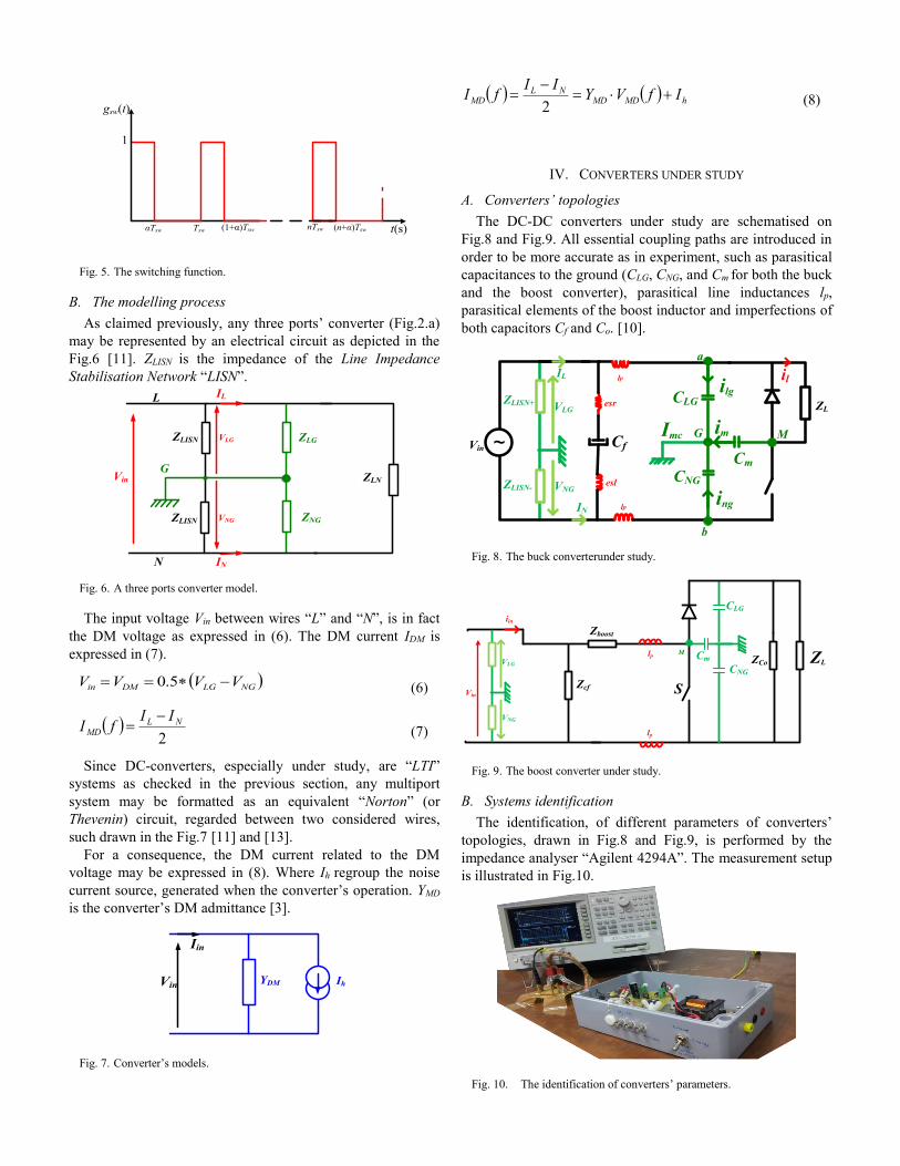
IV. CONVERTERS UNDER STUDY
A. Converters’ topologies
The DC-DC converters under study are schematised on
Fig.8 and Fig.9. All essential coupling paths are introduced in
order to be more accurate as in experiment, such as parasitical
capacitances to the ground (CLG, CNG, and Cm for both the buck
and the boost converter), parasitical line inductances lp,
parasitical elements of the boost inductor and imperfections of
both capacitors Cf and Co. [10].
Cf
ZL
CLG
CNG
Cm
M~Vin
IL
im
ing
il
G
b
esr
esl
lp
lp
ZLISN+
ZLISN-
IN
VNG
VLG
ilg
Imc
a
Fig. 8. The buck converterunder study.
Vin
iin
M
S
Zboost
Zcf
ZCo ZLCm
lp
CLG
CNG
lp
VNG
VLG
Fig. 9. The boost converter under study.
B. Systems identification
The identification, of different parameters of converters’
topologies, drawn in Fig.8 and Fig.9, is performed by the
impedance analyser “Agilent 4294A”. The measurement setup
is illustrated in Fig.10.
Fig. 10. The identification of converters’ parameters.
NGLGDMin VVVV 5.0 (6)
2
NLMD
IIfI
(7)

1) Capacitors’ model identification
The decoupling capacitor’s impedance ZCx (Cx for Cf or Co),
is modelled by three serial elements: the capacitance “Cx”, the
serial inductive element “esl”, and the serial resistive element
“esr” as expressed in (9). Those elements are identified by the
impedance analyser 4294A. Fig.11 shows the comparison
between the model and the measured impedance.
esrpeslpC
PZx
Cx
1
(9)
Fig. 11. The input capacitor’s impedance: (red) the serial element
model,(blue) the measured impedance.
2) Parasitical elements
Converters’ parasitical elements are identified by the
impedance analyser 4294A. The parasitical elements such as,
the line inductances lp, the capacitances to the ground CLG,
CNG and Cm, are deduced from measured impedances of the
Fig.12, depicted between the “L” (or “N”) and the “G” wire.
The Cm capacitance, between the heatsink and the ground, is
estimated according to (10), which is the plane capacitor
equation.
e
sC rm 0 (10)
ε0 and εr are respectively the permittivity of the air and the relative permittivity of the insulator mica (εr=5)
ZLG: impedance between Plus-Ground wires,
ZNG: impedance between Minus-Ground wires,
(a)
(b)
Fig. 12. Impedances of the quadripolar model of the Fig.6: (a) ZLG impedance between Plus-Ground wires, (b) ZNGimpedance between
Minus-Ground wires.
3) Boost inductor
The boost inductor is the essential element in the Boost
converter structure, since it is one which controls the variation
of the current (state variable). Hence, its impedance is not
without effect on the global DM impedance of the converter.
Moreover, the equivalent HF model given in the Fig.13 is
composed by a parallel resistive element “epr” and a parallel
capacitive element “ecp”.
epr
ecp
Lboost
Fig. 13. The equivalent model of the boost inductor Zboost
Fig.14 is the boost inductor impedance measured by the
impedance analyser Agilent 4294A.

Fig. 14. Identification of the boost inductor impedance
V. MODEL APPLYING
A. Equations model applied on the buck converter
In this work, we are not interested to the harmonic source Ih,
expressed in (8) and represented in the Fig.7.
Actually, YLG and YNG, expressed in (2) and appearing in
the model of (8), are parasitical capacitances’ impedances to
the referential conductor “G” [3]; they are expressed,
respectively in (11) and (12).
The measurement is done by an experimental test using the
impedance analyser 4294A. They are not dependent on the
switching phenomena [3, 11].
Note that, in (11) and (12) impedances are an addition of
two terms. The first one, is dependent on the inner capacitance
CLG (or CNG), the second term at (1-α) time, there is an
addition capacitances (Cm of the middle point “M”) which
comes to be added on this inner capacitance. Moreover, the
capacitance Cm is added alternately, sometimes to the
capacitance CLG sometimes to CNG.
YLN expressed in (13), is the switching impedance,
depending on: devices switching, the input capacitor
impedance and the load impedance [3]. Neither CNG nor CLG
are included in the YLN expression.
As a result, the DM impedance of the buck converter is
depicted in the Fig.15, for different operation points,
depending on the duty cycle α. The result is compared to the
decoupling capacitor impedance “ZCf” measured by the
impedance analyser 4294A (yellow colour), and its serial
element synthesised model (in black colour).
Note that this impedance matches with the input capacitor
impedance in yellow colour all along a large frequency band,
until 100MHz.
This result is helpful to identify DC-converters especially at
the design stage.
According to (2), the DM impedance at low frequencies,
trend to be as expressed bellow:
For a consequence, at low frequencies under 100Hz (this
limit depends actually on converter’s components), the DM
converter’s impedance (red and blue colour), depends on the
output load impedance Zl, and varies with the variation of the
duty cycle α (α=0.3, 0.5, 0.8). In other words, it depends on
converter’s operation points.
The resonance appeared around 100MHz, is due to the
interaction between esl of the input capacitor Cf and the
parasitical line impedances lp. This will be detailed in the next
section. After that frequency, the DM impedance takes the
value of parasitical line impedance Zlp.
Fig. 15. The DM Impedance of the buck converter.
B. Model applied on the boost converter
The previous model is also applied on one more system
which is a boost converter, in order to make a comparison and
may be extract a general rule about the EMC converter
identification.
The same analytical process is performed in this case, and is
expressed on (15). Where:
Zboost is the boost inductor impedance,
ZCf is the input capacitor impedance,
ZL is the load impedance,
Zlp is the layout parasitical inductance,
ZC0 is the output capacitor impedance,
ifCCifl
ifCifl
Y
mLG
pLG
p
LG
2
12
1
2
12
(11)
ifCCifl
ifCifl
Y
mNG
pNG
p
NG
2
12
2
12
1
(12)
m swllCfLN
mFfZ
m
ZZY
22
2 sinc1
(13)
2
fZZ lDM (14)
nboostcf
nboostcfDM
KfZfZ
KfZfZZ
(15)
0
20
21sin//1
n
swCswln ncnFfZnFfZK
(16)

The DM impedance of the boost converter is depicted in the
Fig.16 for three duty cycle (α=0.3, 0.5, 0.8) and compared to
the input filter impedance.
It is important to outline that the DM converter’s impedance
matches also here with the input filter impedance ZCf, (red
colour) along the frequency band of interest (150 kHz to
30MHz). Some distinctions appear due to resonances with the
boost inductor around 1.5 kHz. Note that, at low frequencies
(less than 100Hz) the impedance depends also on the duty
cycle α, as outlined in the buck converter case.
Fig. 16. Impedance ZMD of the the boost converter
As showed in the Fig.15 and Fig.16, both spectrums of DM
impedances of the buck or the boost converter give the
impression that they are different –more resonances in the
boost.
However, in a major way it’s necessary to point out that
both impedances are matching the impedance of the input
decoupling capacitors ZCf (red colour), all along a large
frequency band. In other words, the differential mode
impedance YMD of the buck or the boost converter is the same.
As a consequence, the knowledge of the converter
impedance, which is connected directly to the EMC filter, can
significantly enhance its optimisation and therefore reduce the
EMC security margin.
VI. THE EFFECT OF SOME INTRINSIC PARAMETERS
In this section we will study the effect of some parameters
of the buck converter on its DM impedance profile. Equations
(2) and (11–13), reveal that for the buck converter case, the
impedance model depends on some intrinsic converter’s
parameters:
The input capacitor value “Cf”,
The “esl” of the input capacitor “Cf”,
Parasitical capacitances to the ground CLG, CNG and
Cm,
Parasitical capacitances on power devices sides:
the Mosfet capacitance Cds (between the drain and
the source), the diode capacitance Cdiode.
Parasitical line inductances lp,
Those parameters have an actual effect on the impedance
profile evolution in the spectral domain.
A. The effect of the input capacitor Cf
According to (2) and (11–13), the DM impedance depends
on the ZCf impedance, otherwise on the value of the capacitor
Cf.
Two profiles of the DM impedance associated to two input
capacitors’ value are represented and compared on the Fig.17.
Note that there is an obvious difference between the two
profiles. For the blue case (Cf = 10µF), the shape of the DM
impedance seen at low frequencies, as expressed in (14) is
extended until 300Hz, than that recorded for the red case (Cf =
100µF).
Fig. 17. The comparison between two DM impedances profile about two
values of the input capacitors Cf={10µF, 100µF}.
B. The effect of the esl of the capacitor Cf
For the same reason, the serial inductor element of the input
capacitor “esl” has a major impact on the DM impedance
profile especially at high frequencies. This is clearly visible on
the Fig.18, between the blue and the red profiles, around the
band of [1MHz, 100MHz].
Fig. 18. The comparison between two DM impedances profile about two
values of the “esl = {10nH, 50nH}” of the input capacitors Cf.

C. The effect of parasitical capacitances
Parasitical capacitances are the essential coupling path,
supporting the CM current generated by converters, and
throwing to the ground [10].
In this paper, the parasitical capacitances accounted are:
CLG the mutual parasitical capacitances seen
between the “line” wire and the referential plane,
CNG the mutual parasitical capacitances seen
between the “Neutral” wire and the referential
plane,
and Cm the mutual parasitical capacitances seen
between the “middle point” of the switching cell
and the referential plane,
The Fig.19 shows two DM impedance profiles for two
parasitical capacitances values. Those values introduced in the
model of the DM impedance expressed in (2) are
comparatively exaggerated in order to make strongly in
evidence the actual effect.
Note that, there is an impact in the impedance profile,
appeared as resonances around 60MHz.
Fig. 19. The comparison between two DM impedances profile for two values of parasitical capacitances.
D. The effect of capacitances of the switching devices
Switching devices of the buck converter, studied in this
paper (Fig.8), are Diode and Mosfet. Those devices are
coupled to parallel capacitances.
Two profile cases are considered for two values of the
Mosfet capacitances (Cds=50pF and 100pF). The result is
given in Fig.20 and Fig.21.
Note that, there is a significant difference between two
impedances YMD deduced by two capacitances’ values, around
10MHz.
VII. CONCLUSIONS
In this paper we have presented a synthesis of input
impedances of two dc-dc converters’ structures. Results point
out that, the differential mode input impedance are matching
along a large frequency band and are identical to the input
decoupling capacitor. This result is helpful for filter
optimisation.
In addition, we have presented some parameters impact on
this impedance, such as the parasitical capacitances of the
switching devices, the esl of the input capacitor and the
parasitical capacitances to the ground.
The effect of each parameter appears and impact on the DM
impedance profile.
Fig. 20. YMD impedance for two capacitances value of the Mosfet
Fig. 21. Zoom of YMD impedance in the impact frequency zone
REFERENCES
[1] A. ALES, JL. Schanen, D.Moussaoui, J. Roudet, "Experimental Validation of a Novel Analytical Approach about a DC-DC Converter Input Impedance", EPE'2013 ECCE Europe, Lille, France, Septembre 2013.
[2] A. ALES, JL. Schanen, D.Moussaoui, J. Roudet, "Impedances Identification of DC/DC Converters for Network EMC Analysis", IEEE Transactions on Power Electronics, Vol.PP , Issue: 99, page 1, 11 Febrary 2014.
[3] A.ALES, Z. Gouichiche, B. Karouche, D. Moussaoui, J-L. Schanen, J. Roudet, “The Accurate Input Impedances of a DC-DC Converters Connected to the Network “, 2015 IEEE 15th International Conference on Environment and Electrical Engineering (EEEIC), Rome 10-13 June 2015.
[4] M. Foissac, J.L. Schanen, C. Vollaire, “Black box EMC model for power electronics converter”, Energy Conversion Congress and Exposition, 2009. ECCE 2009. IEEE , pp. 3609 – 3615, 20-24 September 2009.
[5] Weichang Cheng, Xiaoying He, Shen Xu, Weifeng Sun, Analysis of common-mode electromagnetic interference noise in a flyback converter using a self-supply power control integrated circuit, Power Electronics, IET (Volume:8 , Issue: 9 ) , pp. 1749 - 1757, 31 août 2015.
[6] H. Bishnoi, A.C Baisden, P. Mattavelli, D. Boroyevich, "Analysis of EMI Terminal Modeling of Switched Power Converters", Power Electronics, IEEE Transactions on, pp 3924 – 3933, vol 27, september 2012.
[7] L. Gerbaud, B.Touré, J.-L. Schanen, J-P Carayon, "Modelling process and optimization of EMC filters for power electronics applications", The international journal for computation and mathematics in electrical and electronic engineering, Vol. 31 Iss: 3, pp.747 - 763, 2012.

[8] Arnold S. de Beer, Member, IEEE, “Noise Source Model for Power Converters Incorporating a Single Source with Imbalance, IEEE International Conference on Industrial Technology (ICIT) 2013, Cape Town, 25-28 Feb. 2013.
[9] Jian Sun, “Input Impedance Analysis of Single-Phase PFC Converters”, Applied Power Electronics Conference and Exposition, 2003. APEC '03. Eighteenth Annual IEEE, vol. 1, pp. 361 – 367, 9-13 February 2003.
[10] N. K. Poon, B.M.H. Pong, C.P. Liu, C.K. Tse, “Essential-coupling-path models for non contact EMI in switching power converters using lumped circuit elements”, Power Electronics, IEEE Transactions on, Vol.18, pp. 686 – 695, 26 March 2003.
[11] A. ALES, JL. Schanen, D.Moussaoui, J. Roudet, "A New Analytical EMC Model of Power Electronics Converters based on Quadripole System: Application to Demonstrate the Mode Decoupling Condition", The Applied on Power Electronics Conference and Exposition, Charlote DC, USA, Mars 2015.
[12] A. Ales, G. Frantz, JL. Schanen, D.Moussaoui, J. Roudet, “Common Mode Impedance of Modern Embedded Networks with Power Electronics Converters", EMC Europe 2013, Brugge, Belgium, Sept 2013.
[13] MA. Cheurfi Belhadj, A.Ales, A. Zaoui, Z. Chebbat, JL.Schanen, J.Roudet, “Analytical Model of DC-DC Converters Based onSwitching Impedances and EMI Sources”, EMC Europe 2016, Wroclow, Pologne, Sept. 2016
Achour Ales received the diploma in
electrical engineering from Ecole
Militaire Polytechnique school, Algiers,
Algeria in 2006. He obtained his Master
in Electrical Engineering from Ecole
Militaire Polytechnique school , Algiers,
Algeria in 2009. He received His Ph.D at
Grenoble University, Grenoble, France since 2015. His current
research interest the Electromagnetic compatibility of the
embedded network and power electronics.
Jean-Luc Schanen (M’99–SM’04) was
born in 1968. He received the Electrical
Engineering Diploma and Ph.D. degrees
from Grenoble Institute of Technology,
Grenoble, France, in 1990 and 1994,
respectively. He is currently a Professor
with Grenoble Institute of Technology. He
has been with the Grenoble Electrical
Engineering Laboratory, St. Martin d’Hères, France, since
1994, working in the field of power electronics. His main
activities concern the technological design of power
converters. His research team uses (or develops if not
available) all kinds of modeling tools in order to improve the
performance of power electronics converters, including
electromagnetic compatibility and thermal aspects.
Prof. Schanen is a Senior Member of the IEEE Power
Electronics Society and IEEE Industry Applications Society,
and was Chairman of the Power Electronics Devices and
Components Committee of the IEEE Industry Applications
Society between 2006 and 2007.
Djelloul Moussaoui graduated in Electrical
Engineering from Ecole Militaire
Polytechnique d'Algiers, Algeria in 1987.
He obtained his Ph.D in Electrical
Engineering from Grenoble Institute of
Technology, France in 1997. He became
Professor in 2010, and is currently leading
research in EMC in Power Electronics.
James Roudet was born in 1962. He holds
PHD (1990) and electrical engineering
diploma (1986). He is Professor at Grenoble
University (Université Joseph Fourier,
France), within the G2ELab (Grenoble
Electrical Engineering Lab), in the field of
power electronics. First research interest
concerned resonant converters. Afterwards,
he promoted EMC activities in the field of power electronics,
and developed a leading activity in the technological design of
power converters. He currently holds the director position of
G2ELab, after several years of leading the power electronics
team.