Analysis of the MIPS 32-bit, pipelined processor using ... Analysis of the MIPS 32-bit, pipelined...
22
1 Analysis of the MIPS 32-bit, pipelined processor using synthesized VHDL Aaron Arthurs ([email protected]), Linh Ngo ([email protected]) Department of Computer Science and Engineering, University of Arkansas Abstract: For large and complicated ASIC designs, it is difficult to read and understand the circuits based on schematic drawings alone; as a result, a hardware description language is much needed for a succinct, descriptive, and human-readable summarization of the circuit. In this paper, we explore VHDL, a hardware description language popular in educational environment. Through the design of a 32-bits pipelined CPU as described in “Computer Organization and Design” by John L. Hennessy and David A. Patterson, we present several VHDL compilers, simulators, and synthesizers that are readily accessible for academic environments. Finally, we perform timing and area analysis the MIPS processor using Xilinx’s SPARTAN3 FPGA device and Virtex4 FPGA device. Introduction: Usually, the easiest way to understand a simple circuit is to study its schematics. From the schematics, we can derive the gate structures, wiring structures, critical paths, and more. However, as the circuits become more complicated, their schematics also become harder to understand due to the heavy amount of wires and gates crossing each other. As a result, it is imperative to find a new method to accurately describe the circuits, yet easy to understand and describe on a reasonable amount of papers. The solution for this problem lies in hardware description language (HDL).
Transcript of Analysis of the MIPS 32-bit, pipelined processor using ... Analysis of the MIPS 32-bit, pipelined...
1
Analysis of the MIPS 32-bit, pipelined processor using synthesized VHDL
Aaron Arthurs ([email protected]), Linh Ngo ([email protected]) Department of Computer Science and Engineering, University of Arkansas
Abstract:
For large and complicated ASIC designs, it is difficult to read and understand the circuits
based on schematic drawings alone; as a result, a hardware description language is much needed
for a succinct, descriptive, and human-readable summarization of the circuit. In this paper, we
explore VHDL, a hardware description language popular in educational environment. Through
the design of a 32-bits pipelined CPU as described in “Computer Organization and Design” by
John L. Hennessy and David A. Patterson, we present several VHDL compilers, simulators, and
synthesizers that are readily accessible for academic environments. Finally, we perform timing
and area analysis the MIPS processor using Xilinx’s SPARTAN3 FPGA device and Virtex4
FPGA device.
Introduction:
Usually, the easiest way to understand a simple circuit is to study its schematics. From
the schematics, we can derive the gate structures, wiring structures, critical paths, and more.
However, as the circuits become more complicated, their schematics also become harder to
understand due to the heavy amount of wires and gates crossing each other. As a result, it is
imperative to find a new method to accurately describe the circuits, yet easy to understand and
describe on a reasonable amount of papers. The solution for this problem lies in hardware
description language (HDL).
2
There are two main varieties of HDL: VHDL (Very high speed IC Hardware Description
Language) and Verilog. Both of them are IEEE standards; however, Verilog is more common in
production environment while VHDL is mostly utilized by educational institutions. This project
will focus on analyzing three general VHDL IDE programs, namely MAX Plus-II, QuickHDL,
and ModelSim Suite, that are accessible for students at the University of Arkansas. Another
VHDL IDE, Xilinx ISE with Mentor’s ModelSim, is also considered in order to fully understand
the potential of VHDL in a professional environment.
VHDL Overview:
Supported by the U.S Department of Defense, VHDL was developed in the early 1980s
and quickly gained the acceptance for not only description and documentation but also design
entry, simulation, and synthesis of large ASICs [4]. In 1987, IEEE started to develop the first
standard for VHDL, and the second revision of this standard was completed in 1993 [4]. In a
sense, VHDL can be thought of as a “programming language” for hardware. While both
computer programming languages and VHDL focus on translating an abstract issue in real life
into commands that machines can understand, the degree of abstraction in VHDL problems are
much simpler and closer to the actual behavior of the electronic circuits. As a result, syntax and
algorithms used in VHDL are very simple and descriptive.
Nowadays, most of the companies manufacturing ASICs have developed their own
VHDL editors based on these standards in order to provide the users with an easy to use tool to
customize their ASICs. For example, Altera has Quartus II and MAX Plus II, while Xilinx has
Xilinx ISE.
3
Case Study: MIPS 32-Bit, Pipelined Processor:
This is the capstone project for computer architecture courses in the University of
Arkansas. Usually, the design is limited to 8 bits; and it is usually created with Mentor Graphics’
design architecture function. In this project, the processor will be designed as closely as possible
to the descriptions in Hennessey’s book in order to realize the full potential of available VHDL
editors.
1. Architecture:
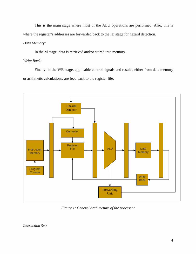
The processor is broken up into five stages: instruction fetch (IF), instructions decode
(ID), execute (EX), data memory (M), and write-back (WB).
Instruction Fetch:
The IF stage involves keeping track of the current/next instruction as well as retrieve the
current instruction from memory. In this scenario, memory is split into separate instruction and
data memories in order to avoid a structural hazard [3]. That is, simultaneous access to memory,
one for instructions and the other for data, is possible in the architecture shown in Figure 1.
Instruction Decode:
On the next cycle, the fetched instruction moves into the ID stage. There, the instruction
is broken up into several fields and inputs into the control logic and register file. Various control
signals, register values, and intermediate values are handed to the EX stage where arithmetic
operations are performed (in this case, integer add and subtract). In addition, the registers’
addresses will be forwarded to the hazard detector in this stage. If there is potential hazard in the
system, this stage will perform a stall.
Execute:
4
This is the main stage where most of the ALU operations are performed. Also, this is
where the register’s addresses are forwarded back to the ID stage for hazard detection.
Data Memory:
In the M stage, data is retrieved and/or stored into memory.
Write Back:
Finally, in the WB stage, applicable control signals and results, either from data memory
or arithmetic calculations, are feed back to the register file.
Figure 1: General architecture of the processor
Instruction Set:
Instruction Memory
Register File
Data
Memory
ALU
Write Back
Program Counter
Controller
Forwarding Unit
Hazard Detector
5
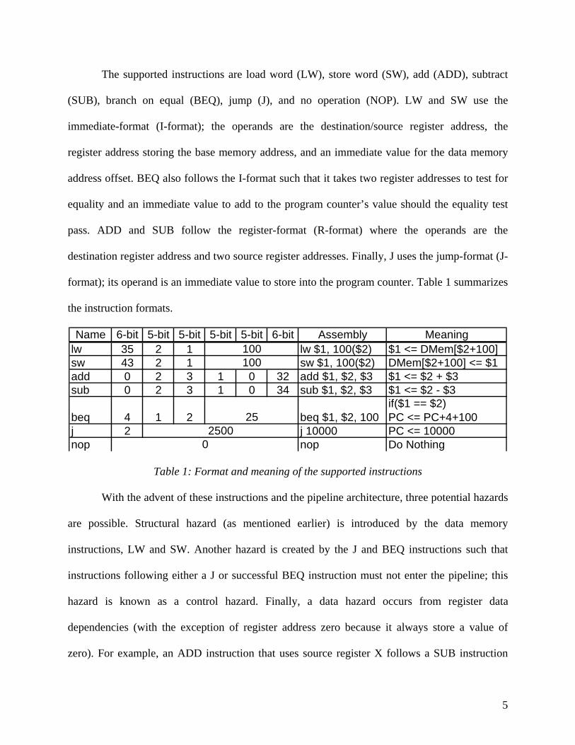
The supported instructions are load word (LW), store word (SW), add (ADD), subtract
(SUB), branch on equal (BEQ), jump (J), and no operation (NOP). LW and SW use the
immediate-format (I-format); the operands are the destination/source register address, the
register address storing the base memory address, and an immediate value for the data memory
address offset. BEQ also follows the I-format such that it takes two register addresses to test for
equality and an immediate value to add to the program counter’s value should the equality test
pass. ADD and SUB follow the register-format (R-format) where the operands are the
destination register address and two source register addresses. Finally, J uses the jump-format (J-
format); its operand is an immediate value to store into the program counter. Table 1 summarizes
the instruction formats.
Name 6-bit 5-bit 5-bit 5-bit 5-bit 6-bit Assembly Meaninglw 35 2 1 lw $1, 100($2) $1 <= DMem[$2+100]sw 43 2 1 sw $1, 100($2) DMem[$2+100] <= $1add 0 2 3 1 0 32 add $1, $2, $3 $1 <= $2 + $3sub 0 2 3 1 0 34 sub $1, $2, $3 $1 <= $2 - $3
beq 4 1 2 beq $1, $2, 100if($1 == $2)PC <= PC+4+100
j 2 j 10000 PC <= 10000nop nop Do Nothing
100100
252500
0
Table 1: Format and meaning of the supported instructions
With the advent of these instructions and the pipeline architecture, three potential hazards
are possible. Structural hazard (as mentioned earlier) is introduced by the data memory
instructions, LW and SW. Another hazard is created by the J and BEQ instructions such that
instructions following either a J or successful BEQ instruction must not enter the pipeline; this
hazard is known as a control hazard. Finally, a data hazard occurs from register data
dependencies (with the exception of register address zero because it always store a value of
zero). For example, an ADD instruction that uses source register X follows a SUB instruction
6
that uses destination register X. The solution used for control hazards is to stall the IF and ID
stages (i.e. force the instructions to be NOP). As for data hazards, the destination register values
kept the M and WB stages are forwarded to the ID and EX stages while the data memory value
from the WB stage is forwarded to the M stage. The forwarding from WB to M is necessary in
case a dependent SW follows a LW instruction.
2. Design method:
This processor is designed using VHDL IEEE 93 standards. Following an object oriented
approach; the components are broken down from the top into smaller blocks that equivalent to
different stages of the pipeline. The blocks are again divided into smaller distinct components
that will be coded in VHDL. There are two main types of components: generic and specific.
Generic components:
These components mostly are the circuits that will be reused again in different blocks. As
a result, generic components are designed with a goal to allow minimize the need for
customization when they are used in different blocks. Multiplexer, flip-flops, and adders are
primary examples for generic components. These components are designed with VHDL’s
GENERIC flag in order to be able to specify the amount of bits needed depending on the bus
size. There are components that are reusable; however, due to their limited amount of usage, they
usually are designed as specific components in order to improve their performance and
testability.
Specific components:
Specific components are stand alone, only-use-once components that need to be specially
customize. Usually, specific components are combinational circuits. In this processor’s design,
hazard detector and forwarding unit are the only two specific components.
7
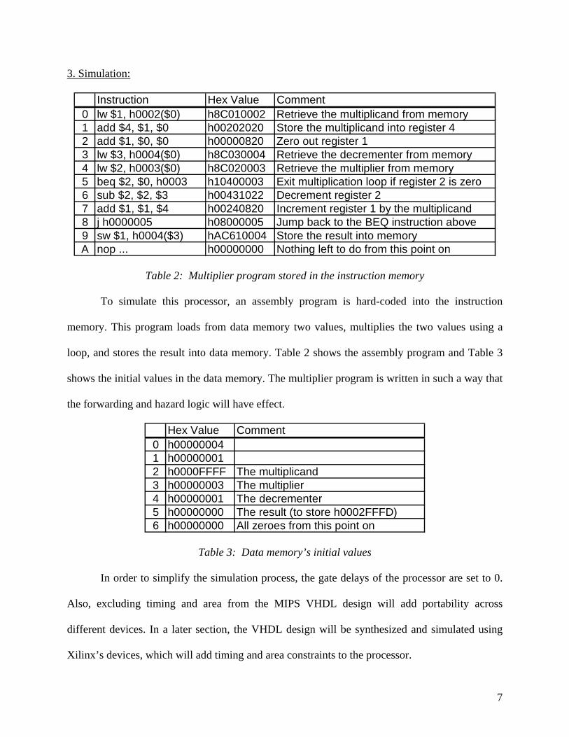
3. Simulation:
Instruction Hex Value Comment0 lw $1, h0002($0) h8C010002 Retrieve the multiplicand from memory1 add $4, $1, $0 h00202020 Store the multiplicand into register 42 add $1, $0, $0 h00000820 Zero out register 13 lw $3, h0004($0) h8C030004 Retrieve the decrementer from memory4 lw $2, h0003($0) h8C020003 Retrieve the multiplier from memory5 beq $2, $0, h0003 h10400003 Exit multiplication loop if register 2 is zero6 sub $2, $2, $3 h00431022 Decrement register 27 add $1, $1, $4 h00240820 Increment register 1 by the multiplicand8 j h0000005 h08000005 Jump back to the BEQ instruction above9 sw $1, h0004($3) hAC610004 Store the result into memoryA nop ... h00000000 Nothing left to do from this point on
Table 2: Multiplier program stored in the instruction memory
To simulate this processor, an assembly program is hard-coded into the instruction
memory. This program loads from data memory two values, multiplies the two values using a
loop, and stores the result into data memory. Table 2 shows the assembly program and Table 3
shows the initial values in the data memory. The multiplier program is written in such a way that
the forwarding and hazard logic will have effect.
Hex Value Comment0 h000000041 h000000012 h0000FFFF The multiplicand3 h00000003 The multiplier4 h00000001 The decrementer5 h00000000 The result (to store h0002FFFD)6 h00000000 All zeroes from this point on
Table 3: Data memory’s initial values
In order to simplify the simulation process, the gate delays of the processor are set to 0.
Also, excluding timing and area from the MIPS VHDL design will add portability across
different devices. In a later section, the VHDL design will be synthesized and simulated using
Xilinx’s devices, which will add timing and area constraints to the processor.
8
Background on Compilers, Simulators, and Synthesizers:
Max+Plus II BASELINE:
MAX+Plus II BASELINE Software is a VHDL editor/simulator program that supports
legacy ASIC designs. Developed by Altera, MAX Plus II can be downloaded and licensed with
no charge. The software allows the users to enter, compile, simulate, and perform timing analysis
on their designs as well as some of Altera’s PLD.
In this project, the CPU was initially designed using MAX Plus II. First of all, MAX Plus
II is easily accessible at computer lab as well as downloadable on home computer. Second, the
graphical interface of MAX is simple and easy to use. However, the devices for which the
software is designed is greatly limited in size; plus, the student’s license does not allow for
partitioning to multiple devices. In addition, many of the needed functions of VHDL such as
generics and array of vectors are not included in MAX. As the design for the CPU grew
gradually complicated, MAX could not handle the complexity of the CPU’s 32 bit structure.
The simulator of MAX is also included in MAX Plus II downloadable copies. However,
due to the legacy features, this simulator would not allow signals inside the circuit to be
generated along the way. The only work around for this shortcoming is to create a different input
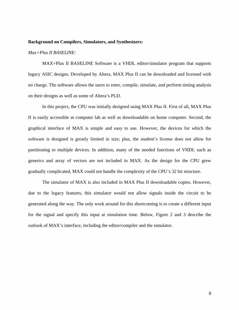
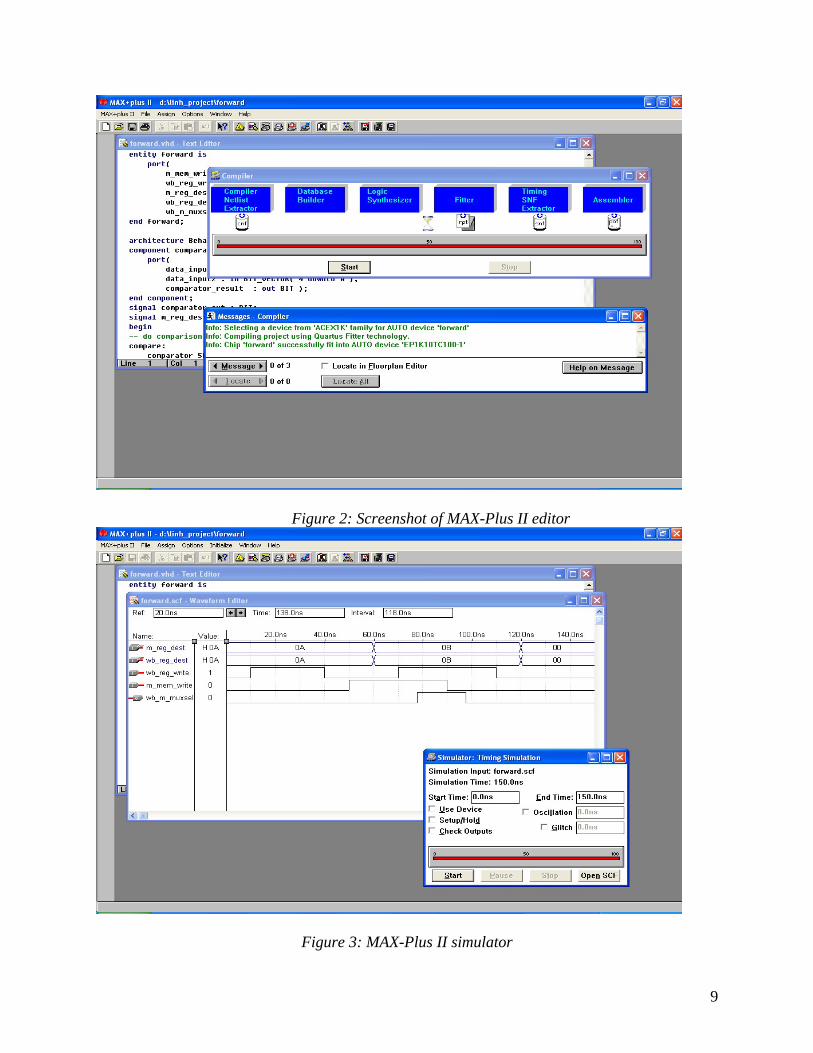
for the signal and specify this input at simulation time. Below, Figure 2 and 3 describe the
outlook of MAX’s interface, including the editor/compiler and the simulator.
9
Figure 2: Screenshot of MAX-Plus II editor
Figure 3: MAX-Plus II simulator
10
Mentor Graphics QuickHDL:
QuickHDL is a command line VHDL compiler and functional simulator running on
Unix/Solaris environments. All the related source codes are required to be in a common
directory, and the user can either manually type or run a script to compile the codes. Flags can
also be added to specific the IEEE standards needed and other user-defined variables.
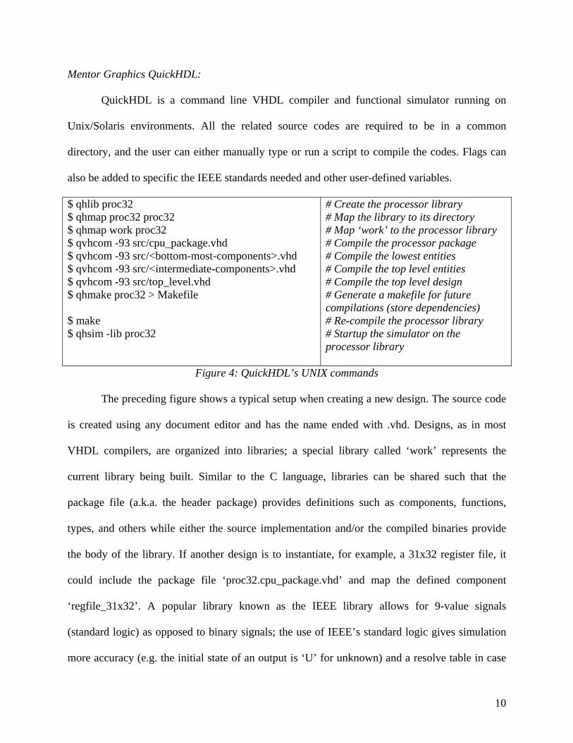
$ qhlib proc32 $ qhmap proc32 proc32 $ qhmap work proc32 $ qvhcom -93 src/cpu_package.vhd $ qvhcom -93 src/<bottom-most-components>.vhd $ qvhcom -93 src/<intermediate-components>.vhd $ qvhcom -93 src/top_level.vhd $ qhmake proc32 > Makefile $ make $ qhsim -lib proc32
# Create the processor library # Map the library to its directory # Map ‘work’ to the processor library # Compile the processor package # Compile the lowest entities # Compile the top level entities # Compile the top level design # Generate a makefile for future compilations (store dependencies) # Re-compile the processor library # Startup the simulator on the processor library
Figure 4: QuickHDL’s UNIX commands
The preceding figure shows a typical setup when creating a new design. The source code
is created using any document editor and has the name ended with .vhd. Designs, as in most
VHDL compilers, are organized into libraries; a special library called ‘work’ represents the
current library being built. Similar to the C language, libraries can be shared such that the
package file (a.k.a. the header package) provides definitions such as components, functions,
types, and others while either the source implementation and/or the compiled binaries provide
the body of the library. If another design is to instantiate, for example, a 31x32 register file, it
could include the package file ‘proc32.cpu_package.vhd’ and map the defined component
‘regfile_31x32’. A popular library known as the IEEE library allows for 9-value signals
(standard logic) as opposed to binary signals; the use of IEEE’s standard logic gives simulation
more accuracy (e.g. the initial state of an output is ‘U’ for unknown) and a resolve table in case
11
two or more signals drive the same line (e.g. bus contention). One more note about IEEE’s
library is that it includes conversion functions for standard logic vectors to scalar values, which
is used in the VHDL design of some of the processor’s components.
Once a library is created and mapped to a certain directory, the source code is compiled.
For a hierarchical design, the package file is compiled first; next, the bottom-most components
(a.k.a. leaf components) are compiled. Then, the components at the next level are compiled and
so forth until the top-most components are compiled. If the top-most components are compiled
before the lower components, the compiler will generate warnings stating that the lower
components are not bonded to the design’s library. Hierarchical designs bring the issue of
dependencies, which not only makes compiling complex designs difficult but also changing the
design. If any of the lower components are changed, then the lower components up to the top-
most components must be re-compiled. QuickHDL includes a command called ‘qhmake’ that
takes a compiled library as an argument and outputs dependencies (redirected to a makefile).
With the dependencies stored, the ‘make’ command can easily re-compile changes in any part of
the library.
Once the library is fully compiled, it is verified through QuickHDL’s functional
simulator, QHSIM. This simulator is event-driven in that it responds to changes in signal values
over a given period of time at a specified interval; another name for this type of simulator is a
discrete event simulator. Events, or signal changes, are time stamped when they occur. These
events can be input manually into the program at run time or typed into a test file before hand.
When the simulation is run, these test files can be loaded and the events will be performed
completely.
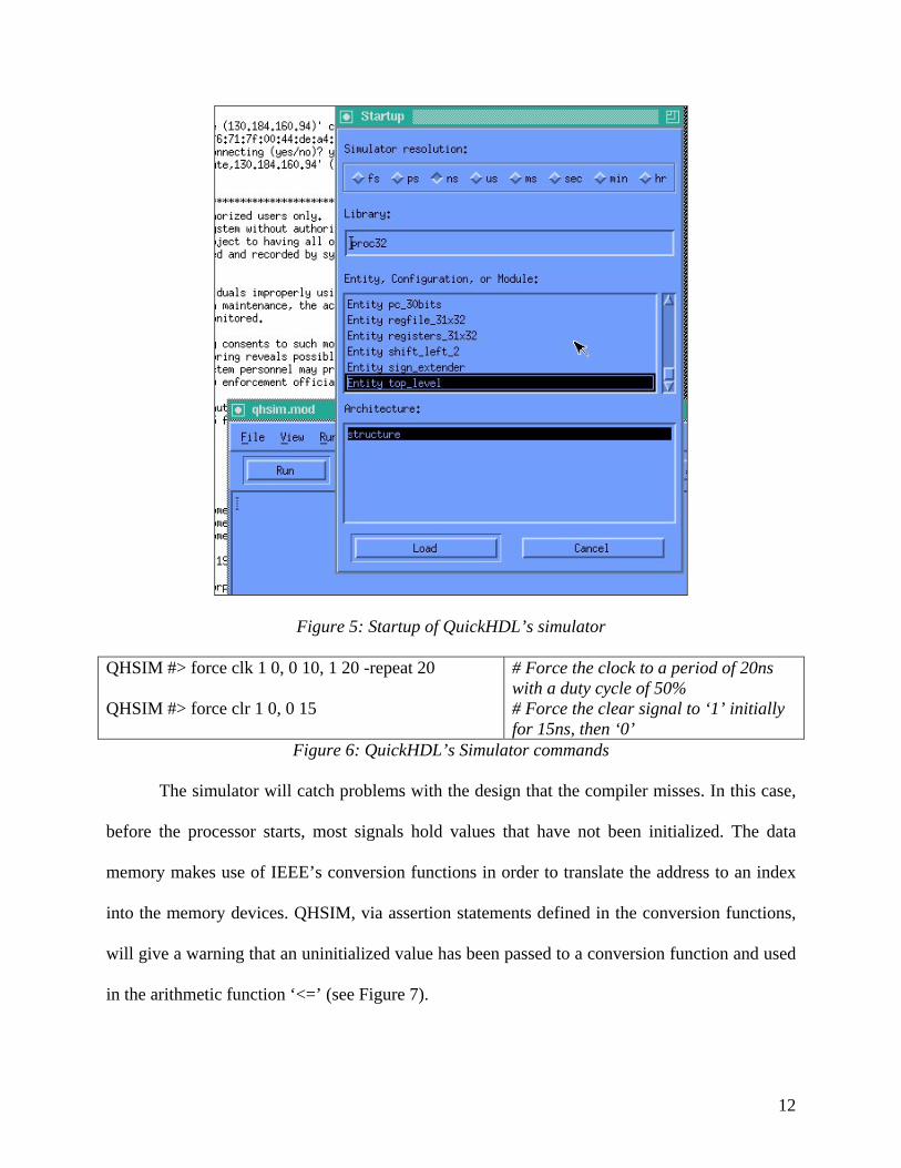
12
Figure 5: Startup of QuickHDL’s simulator
QHSIM #> force clk 1 0, 0 10, 1 20 -repeat 20 QHSIM #> force clr 1 0, 0 15
# Force the clock to a period of 20ns with a duty cycle of 50% # Force the clear signal to ‘1’ initially for 15ns, then ‘0’
Figure 6: QuickHDL’s Simulator commands
The simulator will catch problems with the design that the compiler misses. In this case,
before the processor starts, most signals hold values that have not been initialized. The data
memory makes use of IEEE’s conversion functions in order to translate the address to an index
into the memory devices. QHSIM, via assertion statements defined in the conversion functions,
will give a warning that an uninitialized value has been passed to a conversion function and used
in the arithmetic function ‘<=’ (see Figure 7).
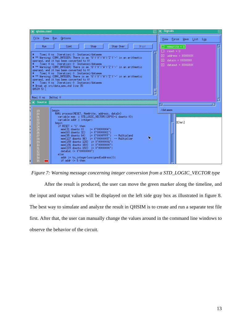
13
Figure 7: Warning message concerning integer conversion from a STD_LOGIC_VECTOR type
After the result is produced, the user can move the green marker along the timeline, and
the input and output values will be displayed on the left side gray box as illustrated in figure 8.
The best way to simulate and analyze the result in QHSIM is to create and run a separate test file
first. After that, the user can manually change the values around in the command line windows to
observe the behavior of the circuit.
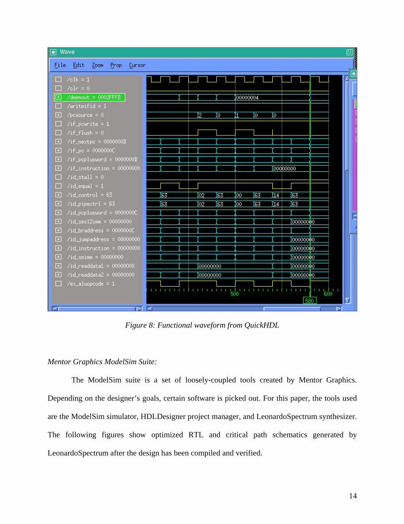
14
Figure 8: Functional waveform from QuickHDL
Mentor Graphics ModelSim Suite:
The ModelSim suite is a set of loosely-coupled tools created by Mentor Graphics.
Depending on the designer’s goals, certain software is picked out. For this paper, the tools used
are the ModelSim simulator, HDLDesigner project manager, and LeonardoSpectrum synthesizer.
The following figures show optimized RTL and critical path schematics generated by
LeonardoSpectrum after the design has been compiled and verified.
15
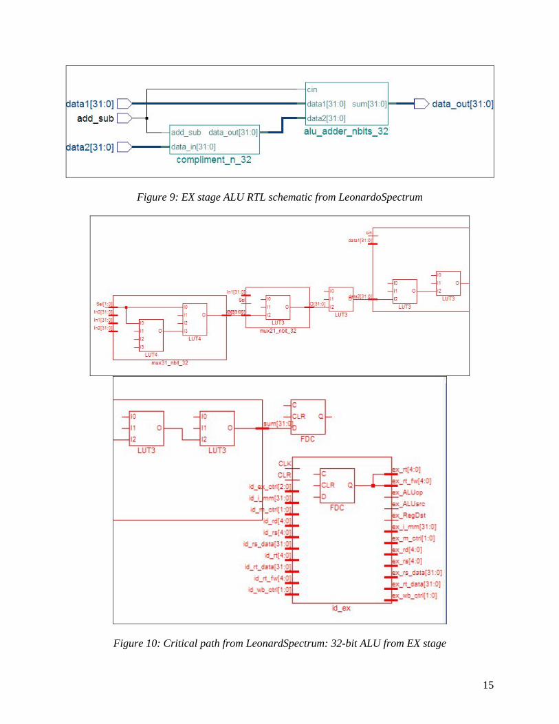
Figure 9: EX stage ALU RTL schematic from LeonardoSpectrum
Figure 10: Critical path from LeonardSpectrum: 32-bit ALU from EX stage
16
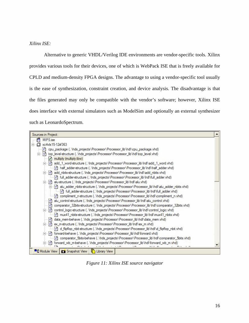
Xilinx ISE:
Alternative to generic VHDL/Verilog IDE environments are vendor-specific tools. Xilinx
provides various tools for their devices, one of which is WebPack ISE that is freely available for
CPLD and medium-density FPGA designs. The advantage to using a vendor-specific tool usually
is the ease of synthesization, constraint creation, and device analysis. The disadvantage is that
the files generated may only be compatible with the vendor’s software; however, Xilinx ISE
does interface with external simulators such as ModelSim and optionally an external synthesizer
such as LeonardoSpectrum.
Figure 11: Xilinx ISE source navigator
17
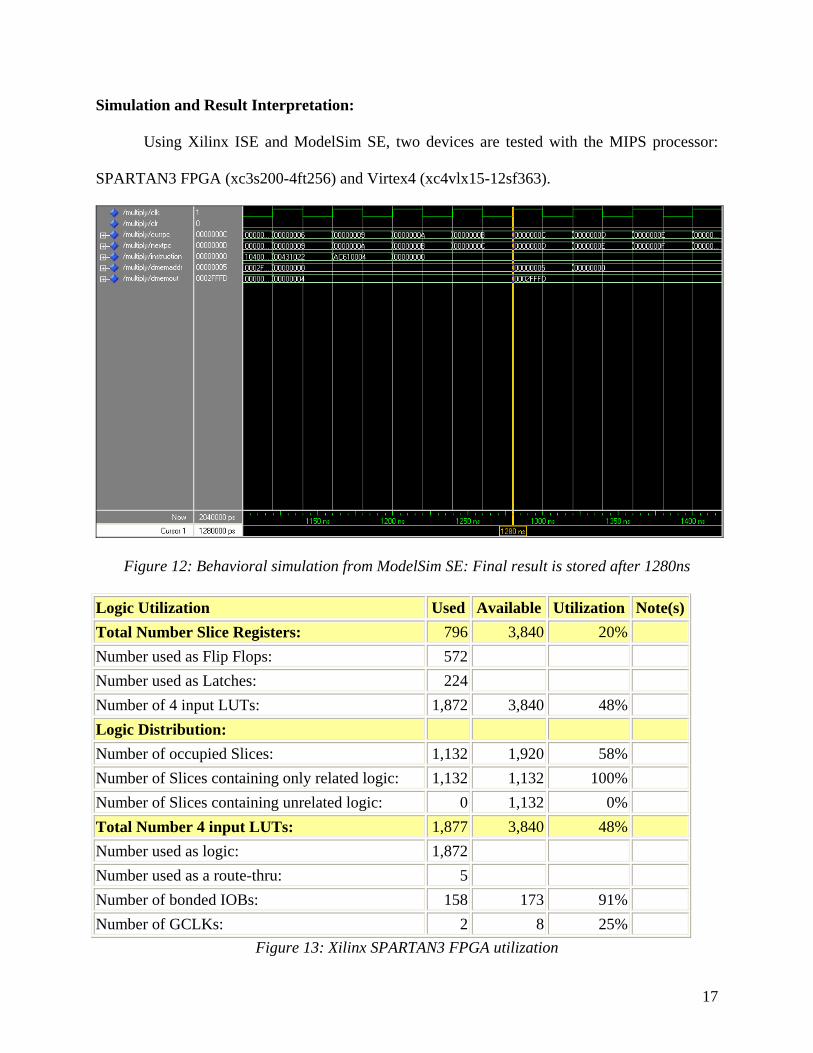
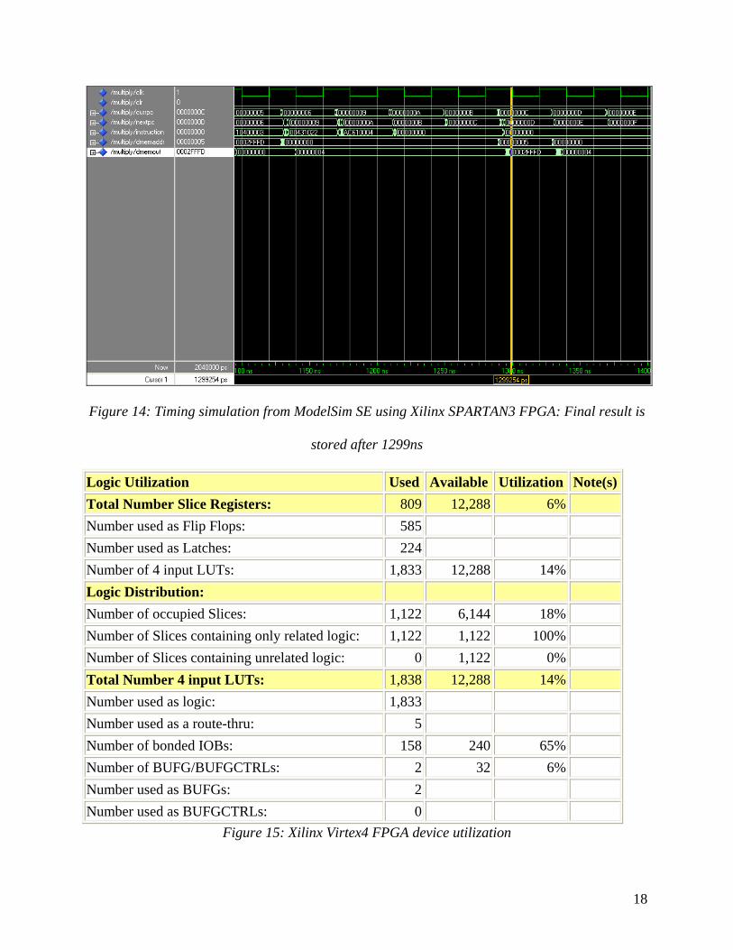
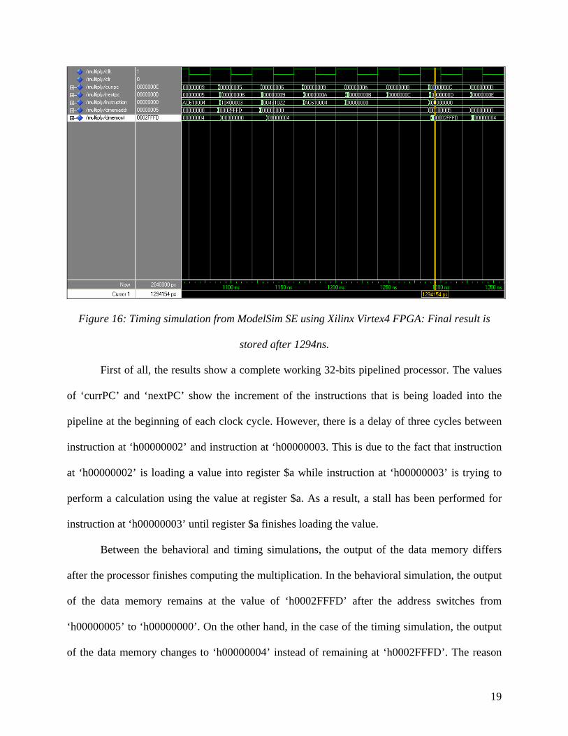
Simulation and Result Interpretation:
Using Xilinx ISE and ModelSim SE, two devices are tested with the MIPS processor:
SPARTAN3 FPGA (xc3s200-4ft256) and Virtex4 (xc4vlx15-12sf363).
Figure 12: Behavioral simulation from ModelSim SE: Final result is stored after 1280ns
Logic Utilization Used Available Utilization Note(s)Total Number Slice Registers: 796 3,840 20% Number used as Flip Flops: 572 Number used as Latches: 224 Number of 4 input LUTs: 1,872 3,840 48% Logic Distribution: Number of occupied Slices: 1,132 1,920 58% Number of Slices containing only related logic: 1,132 1,132 100% Number of Slices containing unrelated logic: 0 1,132 0% Total Number 4 input LUTs: 1,877 3,840 48% Number used as logic: 1,872 Number used as a route-thru: 5 Number of bonded IOBs: 158 173 91% Number of GCLKs: 2 8 25%
Figure 13: Xilinx SPARTAN3 FPGA utilization
18
Figure 14: Timing simulation from ModelSim SE using Xilinx SPARTAN3 FPGA: Final result is
stored after 1299ns
Logic Utilization Used Available Utilization Note(s)Total Number Slice Registers: 809 12,288 6% Number used as Flip Flops: 585 Number used as Latches: 224 Number of 4 input LUTs: 1,833 12,288 14% Logic Distribution: Number of occupied Slices: 1,122 6,144 18% Number of Slices containing only related logic: 1,122 1,122 100% Number of Slices containing unrelated logic: 0 1,122 0% Total Number 4 input LUTs: 1,838 12,288 14% Number used as logic: 1,833 Number used as a route-thru: 5 Number of bonded IOBs: 158 240 65% Number of BUFG/BUFGCTRLs: 2 32 6% Number used as BUFGs: 2 Number used as BUFGCTRLs: 0
Figure 15: Xilinx Virtex4 FPGA device utilization
19
Figure 16: Timing simulation from ModelSim SE using Xilinx Virtex4 FPGA: Final result is
stored after 1294ns.
First of all, the results show a complete working 32-bits pipelined processor. The values
of ‘currPC’ and ‘nextPC’ show the increment of the instructions that is being loaded into the
pipeline at the beginning of each clock cycle. However, there is a delay of three cycles between
instruction at ‘h00000002’ and instruction at ‘h00000003. This is due to the fact that instruction
at ‘h00000002’ is loading a value into register $a while instruction at ‘h00000003’ is trying to
perform a calculation using the value at register $a. As a result, a stall has been performed for
instruction at ‘h00000003’ until register $a finishes loading the value.
Between the behavioral and timing simulations, the output of the data memory differs
after the processor finishes computing the multiplication. In the behavioral simulation, the output
of the data memory remains at the value of ‘h0002FFFD’ after the address switches from
‘h00000005’ to ‘h00000000’. On the other hand, in the case of the timing simulation, the output
of the data memory changes to ‘h00000004’ instead of remaining at ‘h0002FFFD’. The reason
20
behind this is that under the behavioral simulation, the value ‘h0002FFFD’ is stored at addresses
‘h00000005’ (the intended address) and ‘h00000000’ (the unintended address). The signal that
enables writing to data memory remains high long enough so that when the address switches to
‘h00000000’, the current value feeding into the data input is stored; this manner occurs because
the data memory is not synchronized with the global clock. On the other hand, the timing
simulations introduce delay into the signals such that the memory-write-enable signal switches
low before the new address propagates into the M stage. This suggests that within the data
memory, the address input is propagating through more logic (possibly decode logic) than the
memory-write-enable signal; when the memory-write-enable signal goes low, the data memory
blocks writing before the new address value propagates through the memory logic.
Figure 13 and Figure 15 shows the different prelayout analysis for the processor.
Although it might be irrelevant for most of the projects at college levels, this is a useful feature
to have for the students in order to better understand the actual process of designing ASICs in a
professional environment. Studying the above figures, it could be suggested that the SPARTAN3
provides more efficiency in terms of area than the under-utilized Virtex4.
Conclusion and Future Work:
With the easy to use interface of MAX-Plus II, the simple steps of the CPU can be done
and tested with little effort. However, as the project progress to more complicated stages, a
strong and fully featured IDE such as QuickHDL is needed. One draw back of QuickHDL is that
it is completely separated from the simulator; as a result, the users have to run a different
program in order to check the design. In addition, the command line interface on UNIX
environment as well as the cost for the license also limits the use of qvhcom in educational
21
situations. Xilinx, the vendor-specific tool, is also a powerful VHDL IDE and device builder.
With its support for Windows and graphical interfaces, Xilinx would be the best choice among
the compilers analyzed in this paper, especially if Xilinx FPGA devices are available in labs.
Nevertheless, the size of the Xilinx ISE installer (approximately 700MB) can be a slight problem
for anyone who would like to download and try it at home.
For future work, a more accurate model for the instruction and data memories is needed.
The instruction memory can easily be modeled after a ROM chip (e.g. for BIOS bootstrap
systems) and optionally combined with an area in RAM reserved for application instructions; the
data memory can be modeled after either SRAM or DRAM, depending on the size. Also, the
instruction set in this processor needs to be extended to support more arithmetic, logical, and
program control functions. Finally, further analysis calls for integrating the processor into a full
system (e.g. cell phones, PCs, automobile computers, etc.).
22
References:
[1] Altera “MAX-Plus II BASELINE Software.”
http://www.altera.com/products/software/products/legacy/max/sof-emax_baseline.html
[2] T. Gross, J. Hennessy, S. Przybylski, C. Rowen. "Measurement and Evaluation of the
MIPS Architecture and Processor." ACM Transactions on Computer Systems. Volume 6,
Issue 3 (August 1988): p229-57.
[3] J. Hennessy, D. Patterson. Computer Organization and Design: The
Hardware/Software Interface: Second Edition. Morgan Kaufmann Publishers, Inc: San
Francisco, California: 1998.
[4] Smith, Michel John Sebastian. “Application-Specific Integrated Circuits.”
[5] Xilinx Spartan3 Family Datasheet.
http://direct.xilinx.com/bvdocs/publications/ds099.pdf
[6] Xilinx Virtex4 Family Datasheet.
http://direct.xilinx.com/bvdocs/publications/ds112.pdf