
Analysis of material selection on dielectric metasurface ... · Analysis of material selection on...
11
Analysis of material selection on dielectric metasurface performance JIANJI YANG AND JONATHAN A. FAN * Department of Electrical Engineering, Stanford University, Stanford, CA 94305, USA * [email protected] Abstract: Dielectric metasurfaces are ultra-thin devices that can shape optical wavefronts with extreme control. While an assortment of materials possessing a wide range of dielectric constants have been proposed and implemented, the minimum dielectric contrast required for metasurfaces to achieve high-efficiency performance, for a given device function and feature size constraint, is unclear. In this Article, we examine the impact of dielectric material selection on metasurface efficiency at optical frequencies. As a model system, we design transmissive, single-layer periodic metasurfaces (i.e., metagratings) using topology optimization, and we sweep device thickness and light deflection angle for differing material types. We find that for modest deflection angles below 40 degrees, materials with relatively low dielectric constants near 4 can be used to produce metagratings with efficiencies over 80%. However, ultra-high-efficiency devices designed for large deflection angles and multiple functions require materials with high dielectric constants comparable to silicon. We also identify, for all materials, a minimum device thickness required for optimal metagrating performance that scales inversely with dielectric constant. Our work presents materials selection guidelines for high-performance metasurfaces operating at visible and infrared wavelengths. © 2017 Optical Society of America OCIS codes: (230.1950) Diffraction gratings; (160.3918) Metamaterials; (310.6628) Subwavelength structures, nanostructures; (310.6805) Theory and design; (350.4238) Nanophotonics and photonic crystals. References and links 1. N. Yu and F. Capasso, “Flat optics with designer metasurfaces,” Nat. Mater. 13(2), 139–150 (2014). 2. M. Khorasaninejad, W. T. Chen, R. C. Devlin, J. Oh, A. Y. Zhu, and F. Capasso, “Metalenses at visible wavelengths: diffraction-limited focusing and subwavelength resolution imaging,” Science 352(6290), 1190– 1194 (2016). 3. D. Lin, P. Fan, E. Hasman, and M. L. Brongersma, “Dielectric gradient metasurface optical elements,” Science 345(6194), 298–302 (2014). 4. F. Aieta, M. A. Kats, P. Genevet, and F. Capasso, “Multiwavelength achromatic metasurfaces by dispersive phase compensation,” Science 347(6228), 1342–1345 (2015). 5. P. Lalanne, S. Astilean, P. Chavel, E. Cambril, and H. Launois, “Design and fabrication of blazed binary diffractive elements with sampling periods smaller than the structural cutoff,” J. Opt. Soc. Am. A 16(5), 1143 (1999). 6. P. Genevet and F. Capasso, “Holographic optical metasurfaces: a review of current progress,” Rep. Prog. Phys. 78(2), 024401 (2015). 7. M. Khorasaninejad, A. Ambrosio, P. Kanhaiya, and F. Capasso, “Broadband and chiral binary dielectric meta- holograms,” Sci. Adv. 2(5), e1501258 (2016). 8. L. Wang, S. Kruk, H. Tang, T. Li, I. Kravchenko, D. N. Neshev, and Y. S. Kivshar, “Grayscale transparent metasurface holograms,” Optica 3(12), 1504–1505 (2016). 9. P. Lalanne, S. Astilean, P. Chavel, E. Cambril, and H. Launois, “Blazed binary subwavelength gratings with efficiencies larger than those of conventional échelette gratings,” Opt. Lett. 23(14), 1081–1083 (1998). 10. D. Sell, J. Yang, S. Doshay, K. Zhang, and J. A. Fan, “Visible light metasurfaces based on single-crystal silicon,” ACS Photonics 3(10), 1919–1925 (2016). 11. D. Sell, J. Yang, S. Doshay, R. Yang, and J. A. Fan, “Large angle, multi-functional metagratings based on freeform multimode geometries,” Nano Lett. 17(6), 3752–3757 (2017). 12. M. Khorasaninejad, W. Zhu, and K. B. Crozier, “Efficient polarization beam splitter pixels based on a dielectric metasurface,” Optica 2(4), 376–382 (2015). 13. D. Sell, J. Yang, S. Doshay, and J. A. Fan, “Periodic dielectric metasurfaces with high-efficiency, multi- wavelength functionalities,” Adv. Optical Mater. 1700645, (2017). Vol. 25, No. 20 | 2 Oct 2017 | OPTICS EXPRESS 23899 #304679 https://doi.org/10.1364/OE.25.023899 Journal © 2017 Received 11 Aug 2017; revised 15 Sep 2017; accepted 18 Sep 2017; published 20 Sep 2017
-
Upload
nguyendung -
Category
Documents
-
view
230 -
download
0
Transcript of Analysis of material selection on dielectric metasurface ... · Analysis of material selection on...

Analysis of material selection on dielectric metasurface performance
JIANJI YANG AND JONATHAN A. FAN*
Department of Electrical Engineering, Stanford University, Stanford, CA 94305, USA *[email protected]
Abstract: Dielectric metasurfaces are ultra-thin devices that can shape optical wavefronts with extreme control. While an assortment of materials possessing a wide range of dielectric constants have been proposed and implemented, the minimum dielectric contrast required for metasurfaces to achieve high-efficiency performance, for a given device function and feature size constraint, is unclear. In this Article, we examine the impact of dielectric material selection on metasurface efficiency at optical frequencies. As a model system, we design transmissive, single-layer periodic metasurfaces (i.e., metagratings) using topology optimization, and we sweep device thickness and light deflection angle for differing material types. We find that for modest deflection angles below 40 degrees, materials with relatively low dielectric constants near 4 can be used to produce metagratings with efficiencies over 80%. However, ultra-high-efficiency devices designed for large deflection angles and multiple functions require materials with high dielectric constants comparable to silicon. We also identify, for all materials, a minimum device thickness required for optimal metagrating performance that scales inversely with dielectric constant. Our work presents materials selection guidelines for high-performance metasurfaces operating at visible and infrared wavelengths. © 2017 Optical Society of America
OCIS codes: (230.1950) Diffraction gratings; (160.3918) Metamaterials; (310.6628) Subwavelength structures, nanostructures; (310.6805) Theory and design; (350.4238) Nanophotonics and photonic crystals.
References and links
1. N. Yu and F. Capasso, “Flat optics with designer metasurfaces,” Nat. Mater. 13(2), 139–150 (2014). 2. M. Khorasaninejad, W. T. Chen, R. C. Devlin, J. Oh, A. Y. Zhu, and F. Capasso, “Metalenses at visible
wavelengths: diffraction-limited focusing and subwavelength resolution imaging,” Science 352(6290), 1190–1194 (2016).
3. D. Lin, P. Fan, E. Hasman, and M. L. Brongersma, “Dielectric gradient metasurface optical elements,” Science345(6194), 298–302 (2014).
4. F. Aieta, M. A. Kats, P. Genevet, and F. Capasso, “Multiwavelength achromatic metasurfaces by dispersive phase compensation,” Science 347(6228), 1342–1345 (2015).
5. P. Lalanne, S. Astilean, P. Chavel, E. Cambril, and H. Launois, “Design and fabrication of blazed binary diffractive elements with sampling periods smaller than the structural cutoff,” J. Opt. Soc. Am. A 16(5), 1143(1999).
6. P. Genevet and F. Capasso, “Holographic optical metasurfaces: a review of current progress,” Rep. Prog. Phys.78(2), 024401 (2015).
7. M. Khorasaninejad, A. Ambrosio, P. Kanhaiya, and F. Capasso, “Broadband and chiral binary dielectric meta-holograms,” Sci. Adv. 2(5), e1501258 (2016).
8. L. Wang, S. Kruk, H. Tang, T. Li, I. Kravchenko, D. N. Neshev, and Y. S. Kivshar, “Grayscale transparent metasurface holograms,” Optica 3(12), 1504–1505 (2016).
9. P. Lalanne, S. Astilean, P. Chavel, E. Cambril, and H. Launois, “Blazed binary subwavelength gratings with efficiencies larger than those of conventional échelette gratings,” Opt. Lett. 23(14), 1081–1083 (1998).
10. D. Sell, J. Yang, S. Doshay, K. Zhang, and J. A. Fan, “Visible light metasurfaces based on single-crystal silicon,” ACS Photonics 3(10), 1919–1925 (2016).
11. D. Sell, J. Yang, S. Doshay, R. Yang, and J. A. Fan, “Large angle, multi-functional metagratings based on freeform multimode geometries,” Nano Lett. 17(6), 3752–3757 (2017).
12. M. Khorasaninejad, W. Zhu, and K. B. Crozier, “Efficient polarization beam splitter pixels based on a dielectricmetasurface,” Optica 2(4), 376–382 (2015).
13. D. Sell, J. Yang, S. Doshay, and J. A. Fan, “Periodic dielectric metasurfaces with high-efficiency, multi-wavelength functionalities,” Adv. Optical Mater. 1700645, (2017).
Vol. 25, No. 20 | 2 Oct 2017 | OPTICS EXPRESS 23899
#304679 https://doi.org/10.1364/OE.25.023899 Journal © 2017 Received 11 Aug 2017; revised 15 Sep 2017; accepted 18 Sep 2017; published 20 Sep 2017
14. Z. Zhou, J. Li, R. Su, B. Yao, H. Fang, K. Li, L. Zhou, J. Liu, D. Stellinga, C. P. Reardon, T. F. Krauss, and X. Wang, “Efficient silicon metasurfaces for visible light,” ACS Photonics 4(3), 544–551 (2017).
15. S. Liu, G. A. Keeler, J. L. Reno, M. B. Sinclair, and I. Brener, “III–V semiconductor nanoresonators—a new strategy for passive, active, and nonlinear all-dielectric metamaterials,” Adv. Opt. Mater. 4(10), 1457–1462(2016).
16. P. P. Iyer, M. Pendharkar, and J. A. Schuller, “Electrically reconfigurable metasurfaces using heterojunction resonators,” Adv. Opt. Mater. 4(10), 1582–1588 (2016).
17. D. G. Baranov, D. A. Zuev, S. I. Lepeshov, O. V. Kotov, A. E. Krasnok, A. B. Evlyukhin, and B. N. Chichkov, “All-dielectric nanophotonics: the quest for better materials and fabrication techniques,” Optica 4(7), 814–825(2017).
18. Z. Wang, S. He, Q. Liu, and W. Wang, “Visible light metasurfaces based on gallium nitride high contrast gratings,” Opt. Commun. 367, 144–148 (2016).
19. A. Zhan, S. Colburn, R. Trivedi, T. K. Fryett, C. M. Dodson, and A. Majumdar, “Low-contrast dielectricmetasurface optics,” ACS Photonics 3(2), 209–214 (2016).
20. M. S. Seghilani, M. Sellahi, M. Devautour, P. Lalanne, I. Sagnes, G. Beaudoin, M. Myara, X. Lafosse, L. Legratiet, J. Yang, and A. Garnache, “Photonic crystal-based flat lens integrated on a Bragg mirror for High-Q external cavity low noise laser,” Opt. Express 22(5), 5962–5976 (2014).
21. M. P. Bendsoe and O. Sigmund, Topology Optimization: Theory, Methods, and Applications (Springer: Berlin Heidelberg, 2003).
22. J. Lu and J. Vučković, “Nanophotonic computational design,” Opt. Express 21(11), 13351–13367 (2013). 23. J. A. Fan, D. Sell, and J. Yang, “Device components formed of multiple layers of geometric structures or a three
dimensional multi-layer, multi-material metasurface,” U. S. provisional patent No. 62/329,841 (2016). 24. J. Yang, D. Sell, and J. A. Fan, “Freeform metagratings based on complex light scattering dynamics for extreme,
high efficiency beam steering,” Ann. Phys. (Berlin) (2017). 25. J. Yang and J. Fan, “Investigating the impact of initial geometric layout on topology-optimized metagrating
performance,” Opt. Lett. 42, 3161–3164 (2017).26. J. P. Hugonin and P. Lalanne, Reticolo software for grating analysis. Institut d'Optique, Orsay, France (2005). 27. P. Lalanne, J. P. Hugonin, and P. Chavel, “Optical properties of deep lamellar gratings: a coupled Bloch-mode
insight,” J. Lightwave Technol. 24(6), 2442–2449 (2006).28. J. Yang, C. Sauvan, T. Paul, C. Rockstuhl, F. Lederer, and P. Lalanne, “Retrieving the effective parameters of
metamaterials from the single interface scattering problem,” Appl. Phys. Lett. 97(6), 061102 (2010).
1. Introduction
Metasurfaces [1] support amplitude and phase responses that can be tailored in novel and unprecedented ways. They have been used to realize a broad range of transmissive and reflective optical devices, from lenses [2–5] and holograms [6–8] to blazed gratings [3,9–11] and beam splitters [11–13], and can operate at wavelengths spanning the ultraviolet to radio frequencies. Initial metasurface concepts utilized metallic subwavelength-scale structures and targeted mid-infrared operation [1]. These concepts have served as model systems for wavefront engineering, but have been difficult to extend to high-efficiency devices operating at visible and near-infrared wavelengths due to absorption losses intrinsic to metal. Complementary efforts have since been made to realize metasurfaces using dielectric materials [2–4,10,11], which can have low or negligible absorption losses depending on the material and operating wavelength. Dielectric devices have the potential to support high-efficiency operation within the visible regime.
To date, a wide range of dielectric materials have been studied and implemented in metasurfaces. Silicon is amongst the most commonly used materials due to its large dielectric constant and maturity of nanostructuring, and it has been implemented in metasurface design concepts based on Mie resonances [3] and transmit arrays [4]. The operating wavelength range strongly depends on the crystallinity of silicon [10,14]: amorphous and polycrystalline silicon devices can efficiently operate in the infrared and near-infrared wavelength ranges, while single-crystal silicon devices can efficiently function at visible wavelengths due to its relatively low absorption losses. III-V semiconductors with dielectric constants comparable to that of silicon, such as InAs and GaAs, can also serve in high-efficiency mid-infrared and near-infrared metasurfaces [15–17]. For devices operating in the visible spectrum and parts of the ultraviolet spectrum, titanium dioxide [2] and gallium nitride [18] are suitable due to their transparency at those wavelengths, but they have smaller dielectric constants than silicon.
Vol. 25, No. 20 | 2 Oct 2017 | OPTICS EXPRESS 23900
There have also been demonstrations of metasurfaces using even lower dielectric constant materials, such as silicon nitride [19,20].
It is generally believed that metasurfaces require sufficiently large dielectric contrast relative to their background environment to enable the confinement and manipulation of light within nanoscale structures. However, a systematic and quantitative evaluation of material selection is currently lacking, and it is not clear what the minimum required dielectric contrast is for achieving high-efficiency metasurfaces. This criterion is important for understanding the capabilities and limitations of metasurface devices, and it is particularly critical when designing high-performance devices that can bend light to very large angles (e.g., for building high numerical aperture lenses or for wide-angle displays), operate for multiple wavelengths, or both [11,13]. It is also relevant for metasurfaces operating in the visible and ultraviolet spectrum, where available transparent materials have limited dielectric constant values.
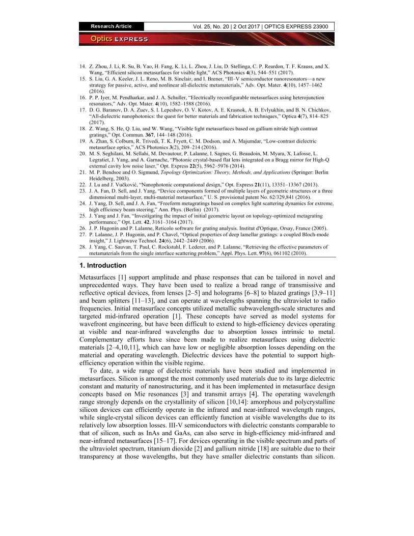
In this Article, we perform a systematic study of metasurfaces made from a wide range of building materials to identify the relationship between material dielectric constant and device performance at optical frequencies. As a model system, we study periodic transmissive metasurfaces (i.e., metagratings) that deflect a normally-incident planewave to particular diffraction orders. For the first part of this study, we analyze devices operating in the near-infrared spectral regime (λ0 = 1800nm) that consist of the following transparent dielectric materials: Ge (n = 4), Si (n = 3.4), TiO2 (n = 2.4), SiN (n = 2.0), Al2O3 (n = 1.7), and SiO2 (n = 1.44). We will examine two classes of metagratings that transmit light to the + 1 diffraction order: two-dimensional devices (Fig. 1(a)), which consist of an array of rectangular nanoridges, and three-dimensional devices (Fig. 1(b)), which consist of fully freeform, curvilinear nanostructures. For the second part of this study, we extend our numerical experiments to the visible spectrum and focus on metagrating deflectors and wavelength splitters based on of crystalline silicon (c-Si) and TiO2. All metagratings in this paper are on a SiO2 substrate.
Fig. 1. Schematics of topology-optimized metagratings. (a) 2D (periodic along x axis) and (b) 3D designs (periodic along x and y axes). For the 3D designs, the y-period is subwavelength-scale, so that diffraction only occurs in x-z plane. In this report, all the metagratings are illuminated by a plane wave at normal incidence. The metagratings are binary structures made of air and the dielectric material, and they are on a SiO2 substrate.
To design these metagratings, we use topology optimization [11,13,21,22], which is an iterative inverse design tool. In this method, an initial device geometry consisting of a random continuum of dielectric constant values is iteratively modified until it converges to a final device consisting of discrete dielectric constant values. In previous work, we showed that single-layer metagratings based on topology optimization support significantly higher efficiencies at large deflection angles, compared to conventional metagratings based on stitched nanoresonators and nanowaveguides [11,13]. We have also extended the use of this design tool to metasurfaces consisting of multiple vertical layers of Si-SiO2 nanostructures, which serve as ultra-high efficiency spectral filters, angular-selective filters, and ultra-wide angle deflectors (>85 degrees) [23]. In this study, we use topology optimization because it does not incorporate any assumptions about the geometric layout or physical operating
Vol. 25, No. 20 | 2 Oct 2017 | OPTICS EXPRESS 23901

mechanisms of our devices [24,25]. Such assumptions, which are made with conventional metasurface designs, restrict the design phase space and make it difficult to objectively compare devices made from different building materials. Rather, with topology optimization, optimal physical operating mechanisms for a given material are readily identified and incorporated into the device designs.
2. Two-dimensional metagratings operating in the near-infrared spectrum
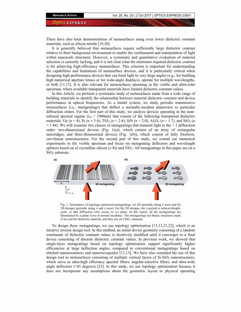
In the first part of this study, we perform a systematic analysis of two-dimensional metagratings, consisting of differing material types, which are designed to preferentially deflect normally-incident TE-polarized light to the + 1 diffraction order. Two-dimensional grating devices are good model systems because they possess a relatively small design phase space, which allows nearly- or fully-optimal metagratings to be identified through brute force simulations. In addition, electromagnetic simulations can be performed quickly and accurately on periodic grating systems using rigorous coupled wave analysis (RCWA) [26], which enables a very large number of topology optimization runs to be performed within reasonable time scales. The efficiencies of optimized metagratings as a function of device thickness, deflection angle, and material type are displayed in Fig. 2(a). To ensure that the devices are compatible with standard fabrication methods, we enforce a minimum feature size within the optimization process to both the ridge width and air gap width. We define this feature size to be 50nm for devices thinner than 1000nm and 1/20th the device thickness for devices thicker than 1000nm. This choice in feature size represents a length scale currently accessible and available in state-of-the-art nanofabrication instrumentation [2].
For each data point in Fig. 2(a), we optimize 200 different devices for a range of device thicknesses and deflection angles ( + 1 diffraction order), each utilizing a different random initial geometry, and select the device with the best efficiency for the plot. Because the efficiencies of topology-optimized devices are sensitive to their initial geometry, only a subset of initial geometries produce final devices with high efficiencies [25]. The deflection efficiency is defined as η = Pdef/Pinc × 100%, where Pdef and Pinc denote the optical power in the deflected beam (representing the desired diffraction order) and incident beam, respectively. Furthermore, to assess whether 200 optimization runs are sufficient for identifying near-optimal devices, we optimize 1000 devices using random initial geometries for two particular metagrating types. The final device efficiency histograms are plotted in Fig. 2(b) and display a narrow distribution of values. We find that more than 40% of the devices have efficiencies that are within 5% of the highest calculated values, for a given device type. Furthermore, a relatively large fraction of random initial geometries converge to the same device with the highest calculated efficiency. Based on these statistics, we anticipate that 200 initial geometries are sufficient for identifying two-dimensional metagratings with near-optimal layouts.
For modest deflection angles, below 40 degrees, materials with a dielectric constant ε larger than 4 support designs with efficiencies higher than 80% (Fig. 2(a)). For SiN (ε = 4.0), these high-efficiency devices require relatively large thicknesses, above 1500nm, which is near the free-space wavelength λ0. The required device thickness for high-efficiency TiO2 metagratings reduces to 900nm (~0.5λ0), and it is further reduced to about 500nm (~0.22λ0) for Si devices. Germanium devices exhibit high efficiencies for thicknesses as thin as 300nm, which represents only 1/6th the free space wavelength. These reductions in minimum device thickness are due in part to the physical reduction of wavelength in dielectric materials, which scales inversely with the refractive index. However, these observed reductions cannot be fully explained by such wave propagation effects, as we empirically find that minimum device thickness scales inversely with the square of refractive index (i.e., dielectric constant), which is a more extreme scaling behavior. We speculate this scaling trend relates to the capability of high dielectric constant metagratings to support multiple scattering, which will be discussed below.
Vol. 25, No. 20 | 2 Oct 2017 | OPTICS EXPRESS 23902
We observe and note that TiO2 devices designed for 30 and 50 degree deflection angles operate with high efficiencies for thicknesses around 500nm. Similar “hot spots” in our contour plots in Fig. 2(a) can also be observed with germanium and silicon. These hot spots appear specific to unique dielectric constant and deflection angle combinations, and their origins will be the topic of future study.
Fig. 2. Absolute deflection efficiency of 2D topology-optimized metagrating deflectors based on different optical materials. (a) Efficiency data from metagratings based on Ge, Si, TiO2, SiN, Al2O3, and SiO2. (b) Histograms of deflection efficiencies for 1000 topology-optimized metagrating deflectors based on Si (left) and TiO2 (right). Si (TiO2) deflectors have thickness t = 1µm (t = 0.8µm) and angle of deflection θ = 50 (θ = 45) degrees. All devices are designed to operate at λ0 = 1800nm. We define absolute efficiency as the deflected power, normalized to the incident power.
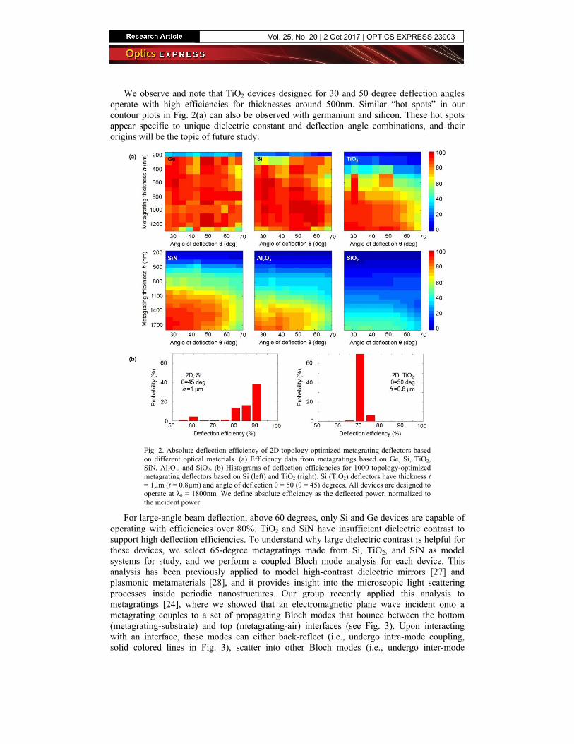
For large-angle beam deflection, above 60 degrees, only Si and Ge devices are capable of operating with efficiencies over 80%. TiO2 and SiN have insufficient dielectric contrast to support high deflection efficiencies. To understand why large dielectric contrast is helpful for these devices, we select 65-degree metagratings made from Si, TiO2, and SiN as model systems for study, and we perform a coupled Bloch mode analysis for each device. This analysis has been previously applied to model high-contrast dielectric mirrors [27] and plasmonic metamaterials [28], and it provides insight into the microscopic light scattering processes inside periodic nanostructures. Our group recently applied this analysis to metagratings [24], where we showed that an electromagnetic plane wave incident onto a metagrating couples to a set of propagating Bloch modes that bounce between the bottom (metagrating-substrate) and top (metagrating-air) interfaces (see Fig. 3). Upon interacting with an interface, these modes can either back-reflect (i.e., undergo intra-mode coupling, solid colored lines in Fig. 3), scatter into other Bloch modes (i.e., undergo inter-mode
Vol. 25, No. 20 | 2 Oct 2017 | OPTICS EXPRESS 23903
coupling, dashed colored lines in Fig. 3), or scatter into free space (red arrows that exit the metagrating in Fig. 3). These modes are orthogonal, and they only interact with each other when they scatter at the top and bottom metagrating interfaces [27].
Fig. 3. Scattering dynamics of Bloch modes associated with metagratings. Inside the metagrating, energy is carried by multiple propagating Bloch modes (M1-Mn), which are excited by an incident plane wave (thick red arrow) from the substrate. The modes bounce between the top and bottom interfaces. At a metagrating interface, a mode can be back-reflected (solid arrows inside the metagrating), excite other Bloch modes (dashed arrows inside the metagrating), or couple to free space diffraction channels (thin red arrows).
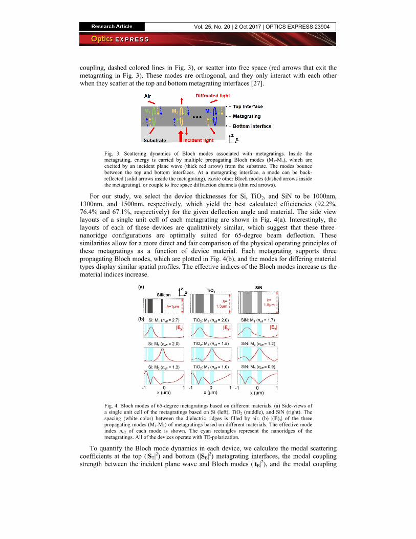
For our study, we select the device thicknesses for Si, TiO2, and SiN to be 1000nm, 1300nm, and 1500nm, respectively, which yield the best calculated efficiencies (92.2%, 76.4% and 67.1%, respectively) for the given deflection angle and material. The side view layouts of a single unit cell of each metagrating are shown in Fig. 4(a). Interestingly, the layouts of each of these devices are qualitatively similar, which suggest that these three-nanoridge configurations are optimally suited for 65-degree beam deflection. These similarities allow for a more direct and fair comparison of the physical operating principles of these metagratings as a function of device material. Each metagrating supports three propagating Bloch modes, which are plotted in Fig. 4(b), and the modes for differing material types display similar spatial profiles. The effective indices of the Bloch modes increase as the material indices increase.
Fig. 4. Bloch modes of 65-degree metagratings based on different materials. (a) Side-views of a single unit cell of the metagratings based on Si (left), TiO2 (middle), and SiN (right). The spacing (white color) between the dielectric ridges is filled by air. (b) |(E)y| of the three propagating modes (M1-M3) of metagratings based on different materials. The effective mode index neff of each mode is shown. The cyan rectangles represent the nanoridges of the metagratings. All of the devices operate with TE-polarization.
To quantify the Bloch mode dynamics in each device, we calculate the modal scattering coefficients at the top (|ST|2) and bottom (|SB|2) metagrating interfaces, the modal coupling strength between the incident plane wave and Bloch modes (|tB|2), and the modal coupling
Vol. 25, No. 20 | 2 Oct 2017 | OPTICS EXPRESS 23904
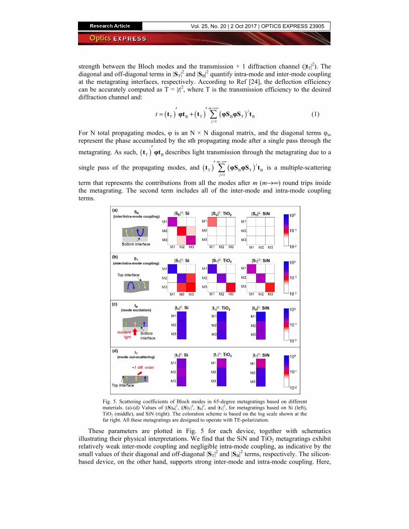
strength between the Bloch modes and the transmission + 1 diffraction channel (|tT|2). The diagonal and off-diagonal terms in |ST|2 and |SB|2 quantify intra-mode and inter-mode coupling at the metagrating interfaces, respectively. According to Ref [24], the deflection efficiency can be accurately computed as T = |t|2, where T is the transmission efficiency to the desired diffraction channel and:
( ) ( ) ( )T B T B T B1
mj
j
t→∞
=
′ ′= + t φt t φS φS t (1)
For N total propagating modes, φ is an N × N diagonal matrix, and the diagonal terms φss represent the phase accumulated by the sth propagating mode after a single pass through the
metagrating. As such, ( )T B
′t φt describes light transmission through the metagrating due to a
single pass of the propagating modes, and ( ) ( )T B T B1
mj
j
→∞
=
′ t φS φS t is a multiple-scattering
term that represents the contributions from all the modes after m (m→∞) round trips inside the metagrating. The second term includes all of the inter-mode and intra-mode coupling terms.
Fig. 5. Scattering coefficients of Bloch modes in 65-degree metagratings based on different materials. (a)-(d) Values of |(S)B|2, |(S)T|2, |tB|2, and |tT|2, for metagratings based on Si (left), TiO2 (middle), and SiN (right). The coloration scheme is based on the log scale shown at the far right. All these metagratings are designed to operate with TE-polarization.
These parameters are plotted in Fig. 5 for each device, together with schematics illustrating their physical interpretations. We find that the SiN and TiO2 metagratings exhibit relatively weak inter-mode coupling and negligible intra-mode coupling, as indicative by the small values of their diagonal and off-diagonal |ST|2 and |SB|2 terms, respectively. The silicon-based device, on the other hand, supports strong inter-mode and intra-mode coupling. Here,
Vol. 25, No. 20 | 2 Oct 2017 | OPTICS EXPRESS 23905
coupling is due to the relatively large effective indices of the modes in the device, together with the relatively tight spatial confinement of the modes within the dielectric ridges. Interestingly, the |tB|2 and |tT|2 terms of the different metagratings are comparable.
The origin of high-efficiency beam deflection in the large-angle silicon metagrating can be traced to multiple-scattering phenomena. If we neglect the multiple-scattering terms in Eq. (1), our calculated efficiency values, using the scattering parameters from Fig. 5, are 51.5% (Si), 64.6% (TiO2), and 62.6% (SiN). If we include these multiple-scattering terms, the deflection efficiencies of the three metagratings become 91.1% (Si), 76.3% (TiO2), and 67.1% (SiN), which agree with the deflection efficiency values (92.2%, 76.4% and 67.1%, respectively) obtained by fully-vectorial calculations. We can clearly see that multiple-scattering substantially improves diffraction efficiency in the Si-based metagratings, but provides only modest improvements to the diffraction efficiencies of the TiO2 and SiN metagratings. We note that these strong multiple-scattering phenomena have also been observed in three-dimensional silicon metagratings and account for the high-efficiency beam steering properties supported by these devices [24].
3. Near infrared three-dimensional metagratings
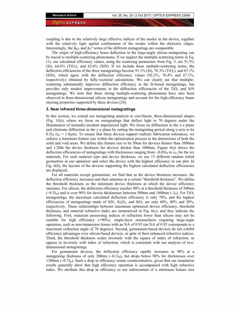
In this section, we extend our metagrating analysis to curvilinear, three-dimensional shapes (Fig. 1(b)), where we focus on metagratings that deflect light to 70 degrees under the illumination of normally-incident unpolarized light. We focus on diffraction in the x-z plane and eliminate diffraction in the y-z plane by setting the metagrating period along y-axis to be 0.5λ0 (λ0 = 1.8µm). To ensure that these devices support realistic fabrication tolerances, we enforce a minimum feature size within the optimization process to the dimensions of both the solid and void areas. We define this feature size to be 50nm for devices thinner than 1000nm and 1/20th the device thickness for devices thicker than 1000nm. Figure 6(a) shows the deflection efficiencies of metagratings with thicknesses ranging from ~0.05λ0 to λ0, for the six materials. For each material type and device thickness, we use 15 different random initial geometries in our optimizer and select the device with the highest efficiency in our plot. In Fig. 6(b), the layouts of the devices supporting the highest calculated deflection efficiencies are displayed.
For all materials except germanium, we find that as the device thickness increases, the deflection efficiency increases and then saturates at a certain “threshold thickness”. We define the threshold thickness as the minimum device thickness at which the device efficiency saturates. For silicon, the deflection efficiency reaches 90% at a threshold thickness of 500nm (~0.3λ0) and is over 90% for device thicknesses between 500nm and 1800nm (~λ0). For TiO2 metagratings, the maximum calculated deflection efficiency is only 70%, and the highest efficiencies of metagratings made of SiN, Al2O3, and SiO2 are only 60%, 40% and 20%, respectively. These relationships between maximum optimized device efficiency, threshold thickness, and material refractive index are summarized in Fig. 6(c), and they indicate the following. First, materials possessing indices of refraction lower than silicon may not be suitable for high efficiency (>90%), single-layer metasurfaces requiring large-angle operation, such as non-immersion lenses with an NA of 0.95 (an NA of 0.95 corresponds to a maximum collection angle of 70 degrees). Second, germanium-based devices do not exhibit efficiency advantages over silicon-based devices, in spite of their enhanced refractive indices. Third, the threshold thickness scales inversely with the square of index of refraction, as oppose to inversely with index of refraction, which is consistent with our analysis of two-dimensional metagratings.
For germanium devices, the deflection efficiency rapidly increases to 90% at a metagrating thickness of only 200nm (~0.1λ0), but drops below 90% for thicknesses over 1300nm (~0.7λ0). Such a drop in efficiency seems counterintuitive, given that our simulation results generally show that high efficiency operation is accompanied with high refractive index. We attribute this drop in efficiency to our enforcement of a minimum feature size
Vol. 25, No. 20 | 2 Oct 2017 | OPTICS EXPRESS 23906
constraint, which prevents our designs from supporting ultra-fine spatial features. Such fine features in thick, high-index devices are generally required to fully control the effective refractive index of propagating modes within waveguide-based metasurfaces. This requirement has been observed in conventional phase-array-based meta-devices that utilize nanowaveguides [2,5,9], and it evidently applies to our topology-optimized devices.
Fig. 6. Performance of 3D, 70-degree metagrating deflectors. (a) Deflection efficiencies of metagratings made of different optical materials as a function of device height. The materials include Ge (red), Si (blue), TiO2 (green), SiN (black), Al2O3 (orange), and SiO2 (magenta). The markers represent simulated efficiency values and the solid curves are trend lines. The metagratings are illuminated by normally incident unpolarized light. (b) Layouts (top view) of the individual unit cells of the highest-efficiency metagratings for a given material. The thicknesses of these devices are 0.7µm (Ge), 1µm (Si), 1.6µm (TiO2), 1.8µm (SiN), 1.6µm (Al2O3), and 1.8µm (SiO2). The spacing (white color) between the dielectric structures is filled by air. (c) Plots of highest device efficiency (blue triangles, left axes) and threshold device thickness (red circles, right axes) as a function of the metagrating material refractive index. The red solid line is a fitted curve. (d) Distribution of calculated efficiencies from 200 Si (blue wide bars) and TiO2 (green narrow bars) metagrating deflectors, each designed with different initial random configurations. In (d), the device thickness is h = 1.2µm and the operating wavelength is λ0 = 1800nm. The definition of efficiency can be found in the caption of Fig. 2.
To gauge whether 15 simulations are sufficient to properly evaluate each device type, we perform 200 simulations of Si and TiO2 70-degree deflectors with a thickness of 1200nm, using random starting points. Histograms of these distributions are plotted in Fig. 6(d) and indicate that more than 50% of the devices have efficiencies that are within 5% of the best calculated values (i.e., 95% for Si-metagratings and 70% for TiO2-metagratings). This indicates that 15 simulations are sufficient for identifying near-optimal devices.
4. Three-dimensional metagratings at visible frequencies
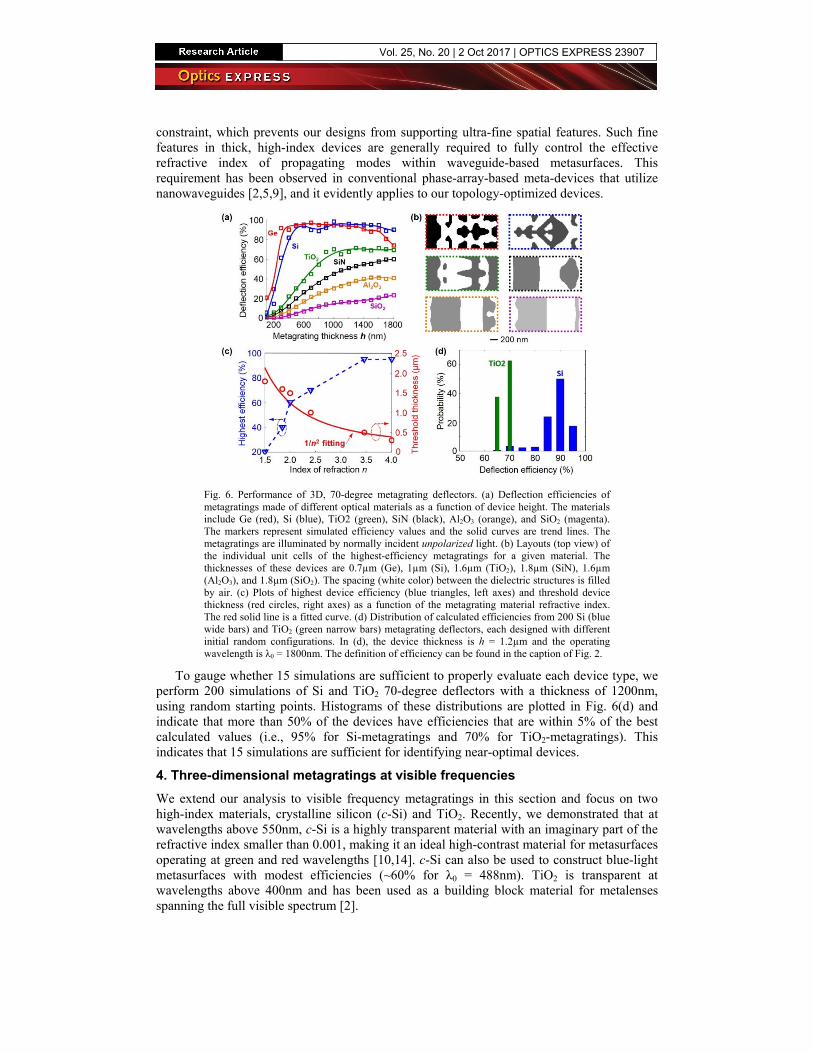
We extend our analysis to visible frequency metagratings in this section and focus on two high-index materials, crystalline silicon (c-Si) and TiO2. Recently, we demonstrated that at wavelengths above 550nm, c-Si is a highly transparent material with an imaginary part of the refractive index smaller than 0.001, making it an ideal high-contrast material for metasurfaces operating at green and red wavelengths [10,14]. c-Si can also be used to construct blue-light metasurfaces with modest efficiencies (~60% for λ0 = 488nm). TiO2 is transparent at wavelengths above 400nm and has been used as a building block material for metalenses spanning the full visible spectrum [2].
Vol. 25, No. 20 | 2 Oct 2017 | OPTICS EXPRESS 23907
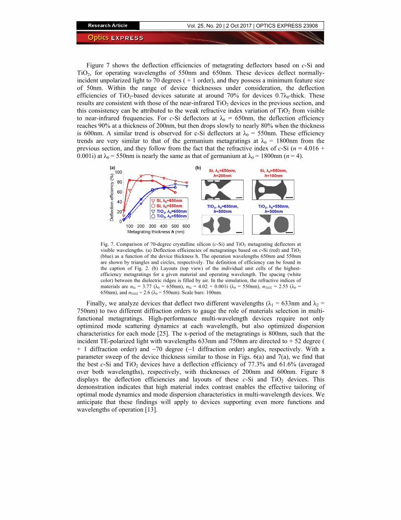
Figure 7 shows the deflection efficiencies of metagrating deflectors based on c-Si and TiO2, for operating wavelengths of 550nm and 650nm. These devices deflect normally-incident unpolarized light to 70 degrees ( + 1 order), and they possess a minimum feature size of 50nm. Within the range of device thicknesses under consideration, the deflection efficiencies of TiO2-based devices saturate at around 70% for devices 0.7λ0-thick. These results are consistent with those of the near-infrared TiO2 devices in the previous section, and this consistency can be attributed to the weak refractive index variation of TiO2 from visible to near-infrared frequencies. For c-Si deflectors at λ0 = 650nm, the deflection efficiency reaches 90% at a thickness of 200nm, but then drops slowly to nearly 80% when the thickness is 600nm. A similar trend is observed for c-Si deflectors at λ0 = 550nm. These efficiency trends are very similar to that of the germanium metagratings at λ0 = 1800nm from the previous section, and they follow from the fact that the refractive index of c-Si (n = 4.016 + 0.001i) at λ0 = 550nm is nearly the same as that of germanium at λ0 = 1800nm (n = 4).
Fig. 7. Comparison of 70-degree crystalline silicon (c-Si) and TiO2 metagrating deflectors at visible wavelengths. (a) Deflection efficiencies of metagratings based on c-Si (red) and TiO2 (blue) as a function of the device thickness h. The operation wavelengths 650nm and 550nm are shown by triangles and circles, respectively. The definition of efficiency can be found in the caption of Fig. 2. (b) Layouts (top view) of the individual unit cells of the highest-efficiency metagratings for a given material and operating wavelength. The spacing (white color) between the dielectric ridges is filled by air. In the simulation, the refractive indices of materials are nSi = 3.77 (λ0 = 650nm), nSi = 4.02 + 0.001i (λ0 = 550nm), nTiO2 = 2.55 (λ0 = 650nm), and nTiO2 = 2.6 (λ0 = 550nm). Scale bars: 100nm.
Finally, we analyze devices that deflect two different wavelengths (λ1 = 633nm and λ2 = 750nm) to two different diffraction orders to gauge the role of materials selection in multi-functional metagratings. High-performance multi-wavelength devices require not only optimized mode scattering dynamics at each wavelength, but also optimized dispersion characteristics for each mode [25]. The x-period of the metagratings is 800nm, such that the incident TE-polarized light with wavelengths 633nm and 750nm are directed to + 52 degree (+ 1 diffraction order) and −70 degree (−1 diffraction order) angles, respectively. With aparameter sweep of the device thickness similar to those in Figs. 6(a) and 7(a), we find that the best c-Si and TiO2 devices have a deflection efficiency of 77.3% and 61.6% (averaged over both wavelengths), respectively, with thicknesses of 200nm and 600nm. Figure 8 displays the deflection efficiencies and layouts of these c-Si and TiO2 devices. This demonstration indicates that high material index contrast enables the effective tailoring of optimal mode dynamics and mode dispersion characteristics in multi-wavelength devices. We anticipate that these findings will apply to devices supporting even more functions and wavelengths of operation [13].
Vol. 25, No. 20 | 2 Oct 2017 | OPTICS EXPRESS 23908
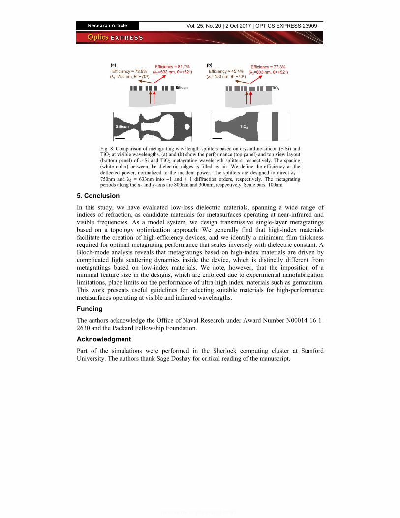
Fig. 8. Comparison of metagrating wavelength-splitters based on crystalline-silicon (c-Si) and TiO2 at visible wavelengths. (a) and (b) show the performance (top panel) and top view layout (bottom panel) of c-Si and TiO2 metagrating wavelength splitters, respectively. The spacing (white color) between the dielectric ridges is filled by air. We define the efficiency as the deflected power, normalized to the incident power. The splitters are designed to direct λ1 = 750nm and λ2 = 633nm into −1 and + 1 diffraction orders, respectively. The metagrating periods along the x- and y-axis are 800nm and 300nm, respectively. Scale bars: 100nm.
5. Conclusion
In this study, we have evaluated low-loss dielectric materials, spanning a wide range of indices of refraction, as candidate materials for metasurfaces operating at near-infrared and visible frequencies. As a model system, we design transmissive single-layer metagratings based on a topology optimization approach. We generally find that high-index materials facilitate the creation of high-efficiency devices, and we identify a minimum film thickness required for optimal metagrating performance that scales inversely with dielectric constant. A Bloch-mode analysis reveals that metagratings based on high-index materials are driven by complicated light scattering dynamics inside the device, which is distinctly different from metagratings based on low-index materials. We note, however, that the imposition of a minimal feature size in the designs, which are enforced due to experimental nanofabrication limitations, place limits on the performance of ultra-high index materials such as germanium. This work presents useful guidelines for selecting suitable materials for high-performance metasurfaces operating at visible and infrared wavelengths.
Funding
The authors acknowledge the Office of Naval Research under Award Number N00014-16-1-2630 and the Packard Fellowship Foundation.
Acknowledgment
Part of the simulations were performed in the Sherlock computing cluster at Stanford University. The authors thank Sage Doshay for critical reading of the manuscript.
Vol. 25, No. 20 | 2 Oct 2017 | OPTICS EXPRESS 23909


![Chiral All-Dielectric Metasurface Based on Elliptic …downloads.hindawi.com/journals/ijap/aip/6352418.pdffunctionalities [8-16] were developed for several microwave THz, and optical](https://static.fdocuments.in/doc/165x107/5b1cde667f8b9af2348c3bc4/chiral-all-dielectric-metasurface-based-on-elliptic-8-16-were-developed-for-several.jpg)


