Analysis of Floating Body Effects in SOI Transistor · 2016-06-20 · floating body effects on...
9
International Research Journal of Engineering and Technology (IRJET) e-ISSN: 2395 -0056 Volume: 03 Issue: 05 | May-2016 www.irjet.net p-ISSN: 2395-0072 © 2016, IRJET | Impact Factor value: 4.45 | ISO 9001:2008 Certified Journal | Page 1123 Analysis of Floating Body Effects in SOI Transistor Abhishek Chauhan 1 , Aditya prakash 2 1 student, Dept. of Electronics and Communication engineering, JIIT University, sector-62, Noida 2 student, Dept. of Electronics and Communication engineering, JIIT University, sector-62, Noida ---------------------------------------------------------------------***------------------------------------------------------------- Abstarct - The work presents the newly deploying technology in semiconductor industry called silicon on insulator (SOI). Its two technology partially and fully depleted SOI and describe how these are different from conventional bulk MOS technology, advantages over bulk technology and floating body effect of PD/FD SOI technology, factors effecting floating body such as kink effects in PD SOI, parasitic bipolar effects in FD SOI and merits/demerits of PD SOI/FDSOI. On the later part we have discussed effect of floating body effects on circuits and methods of suppression of these effects. Key Words: CMOS, FDSOI, PDSOI, Floating body effect, Kink effect. 1. INTRODUCTION Silicon on Insulator is a semiconductor technology which is now used as an technology for chip designing in almost all highly reliable/efficient in both digital and analog electronic systems. Till now the bulk technology is the leading technology in the electronics industry but due to following reasons such as latch up, parasitic capacitance and leakage currents in bulk technology fail to continue in developing highly effective devices as size is reducing. So, at the some lower nodes BULK technology became bottleneck .These effects became so worsen that performance of system gets reduced .so, due to all these reasons SOI became the trustable technology because these effects gets reduced in this technology due the the different structure of SOI .The design rules which help in developing SOI technology was extracted from bulk technology by incorporating oxide layer over the silicon substrate, several problem has solved such as leakage currents, latch up problems ,variation of threshold voltage due to small channel effects. A new device architectures allow better electrical properties to be obtained for low power and high energy efficient and reliable circuits. In this technology an interesting thing is that the body terminal is either tied to gate or left free for floating called as ―floating body. The floating body has some important features in reducing power consumption and improving the device efficiency, about these features an important description is shown in upcoming sections and the reasons for the body tied are also shown. 2. ADVANTAGES OF SOI OVER BULK TECHNOLOGY The description of SOI technology is described briefly in [1]. SOI advantages is given below, according to these advantages it has been given clearly that what factors are superior to bulk technology and is described for each and every advantage. 2.1 SOI Advantages The SOI wafer structure has several important advantages over bulk or epitaxial starting wafer architectures. SOI wafers potentially offer ―perfect transistor isolation (lower leakage), higher transistor packing density, reduced parasitic drain capacitance (faster circuit performance and lower power consumption), and simplified processing relative to bulk or epitaxial silicon wafers. Due to these advantages, SOI wafers appear ideal for future integrated circuits with high speed, high package density, low voltage/low power operation, and battery operated systems requirements, such as portable logic or microprocessor ICs and many other digital and analog systems.Silicon-on-insulator (SOI) wafers have traditionally been used for extreme environmental applications, such as high temperature and severe environments (e.g., outer space). However, they are expected to expand into mainstream CMOS applications due to these advantages. 2.1.1 Negligible drain to source capacitance Fig.1 shows a schematic diagram of the capacitances in bulk-Si and SOI MOSFETs. In SOI devices, the capacitance between the drain (source) and the substrate is negligibly small because of the dielectric constant of SiO2, which is lower than that of Si, and the thickness of the BOX. This helps improve the switching speed of CMOS devices as can be seen in the relationship between power consumption and access time for a 4-Mb SRAM in Fig2[1]. For a given access speed, SOI devices consume only one-half to one- third the power of bulk Si devices; and for a given power consumption, they are 20% to 25% faster. This amount of improvement is typical for SOI CMOS.
Transcript of Analysis of Floating Body Effects in SOI Transistor · 2016-06-20 · floating body effects on...
International Research Journal of Engineering and Technology (IRJET) e-ISSN: 2395 -0056
Volume: 03 Issue: 05 | May-2016 www.irjet.net p-ISSN: 2395-0072
© 2016, IRJET | Impact Factor value: 4.45 | ISO 9001:2008 Certified Journal | Page 1123
Analysis of Floating Body Effects in SOI Transistor Abhishek Chauhan1, Aditya prakash2
1 student, Dept. of Electronics and Communication engineering, JIIT University, sector-62, Noida 2 student, Dept. of Electronics and Communication engineering, JIIT University, sector-62, Noida
---------------------------------------------------------------------***-------------------------------------------------------------
Abstarct - The work presents the newly deploying technology in semiconductor industry called silicon on insulator (SOI). Its two technology partially and fully depleted SOI and describe how these are different from conventional bulk MOS technology, advantages over bulk technology and floating body effect of PD/FD SOI technology, factors effecting floating body such as kink effects in PD SOI, parasitic bipolar effects in FD SOI and merits/demerits of PD SOI/FDSOI. On the later part we have discussed effect of floating body effects on circuits and methods of suppression of these effects.
Key Words: CMOS, FDSOI, PDSOI, Floating body effect, Kink effect.
1. INTRODUCTION
Silicon on Insulator is a semiconductor technology which is now used as an technology for chip designing in almost all highly reliable/efficient in both digital and analog electronic systems. Till now the bulk technology is the leading technology in the electronics industry but due to following reasons such as latch up, parasitic capacitance and leakage currents in bulk technology fail to continue in developing highly effective devices as size is reducing. So, at the some lower nodes BULK technology became bottleneck .These effects became so worsen that performance of system gets reduced .so, due to all these reasons SOI became the trustable technology because these effects gets reduced in this technology due the the different structure of SOI .The design rules which help in developing SOI technology was extracted from bulk technology by incorporating oxide layer over the silicon substrate, several problem has solved such as leakage currents, latch up problems ,variation of threshold voltage due to small channel effects. A new device architectures allow better electrical properties to be obtained for low power and high energy efficient and reliable circuits. In this technology an interesting thing is that the body terminal is either tied to gate or left free for floating called as ―floating body. The floating body has some important features in reducing power consumption and improving the device efficiency, about these features an important description is shown in upcoming sections and the reasons for the body tied are also shown.
2. ADVANTAGES OF SOI OVER BULK TECHNOLOGY
The description of SOI technology is described briefly in [1]. SOI advantages is given below, according to these advantages it has been given clearly that what factors are superior to bulk technology and is described for each and every advantage.
2.1 SOI Advantages
The SOI wafer structure has several important advantages over bulk or epitaxial starting wafer architectures. SOI wafers potentially offer ―perfect transistor isolation (lower leakage), higher transistor packing density, reduced parasitic drain capacitance (faster circuit performance and lower power consumption), and simplified processing relative to bulk or epitaxial silicon wafers. Due to these advantages, SOI wafers appear ideal for future integrated circuits with high speed, high package density, low voltage/low power operation, and battery operated systems requirements, such as portable logic or microprocessor ICs and many other digital and analog systems.Silicon-on-insulator (SOI) wafers have traditionally been used for extreme environmental applications, such as high temperature and severe environments (e.g., outer space). However, they are expected to expand into mainstream CMOS applications due to these advantages.
2.1.1 Negligible drain to source capacitance
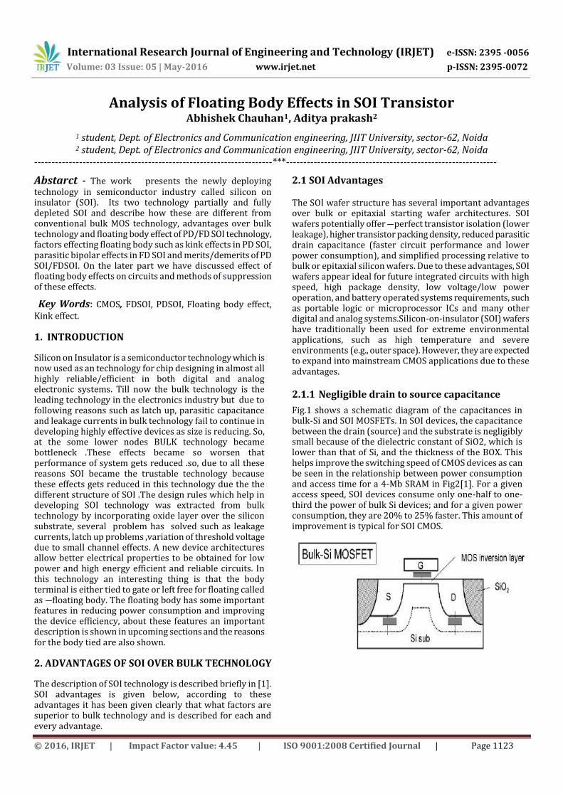
Fig.1 shows a schematic diagram of the capacitances in bulk-Si and SOI MOSFETs. In SOI devices, the capacitance between the drain (source) and the substrate is negligibly small because of the dielectric constant of SiO2, which is lower than that of Si, and the thickness of the BOX. This helps improve the switching speed of CMOS devices as can be seen in the relationship between power consumption and access time for a 4-Mb SRAM in Fig2[1]. For a given access speed, SOI devices consume only one-half to one-third the power of bulk Si devices; and for a given power consumption, they are 20% to 25% faster. This amount of improvement is typical for SOI CMOS.

International Research Journal of Engineering and Technology (IRJET) e-ISSN: 2395 -0056
Volume: 03 Issue: 05 | May-2016 www.irjet.net p-ISSN: 2395-0072
© 2016, IRJET | Impact Factor value: 4.45 | ISO 9001:2008 Certified Journal | Page 1124
Fig -1: Capacitances of bulk-si mosfet and SOI mosfet.
2.1.2 Latch up elimination
Latch-up occurs when the parasitic p-n-p-n (or n-p-n-p) or thyristor in a CMOS structure turns on, which limits the maximum operating voltage. Fig3. shows that, unlike a bulk-Si device, there is no parasitic thyristor in an SOI device. As a result, it is immune to latch-up; and thus there is no need for either a special circuit layout to prevent latch-up or a special device process, such as one to create a buried low-resistivity region.
Fig 2 - Speed and power consumption in SI-mosfet and in SOI
Fig -5: Soft Error immunity of SOI DRAM.
Fig -3: Unlike bulk devices SOI devices has no parasitic thyristor formation so latch up free.
2.1.3 Good soft errors immunity
SOI devices have excellent radiation hardness to alpha particles, neutrons, and other particles. Alpha particles are generated by small amounts of radioactive elements in IC materials. They have an energy of approximately 5 MeV, which enables them to penetrate Si to a depth of about 25 μm. Along the trajectory, they generate electron-hole pairs, which results in negative and positive charges of around 10 fC in every micron. This is sufficient to destroy the memory charge of a DRAM cell or upset the memory state of an SRAM. Neutrons generated by secondary cosmic rays also induce soft errors [2]. So, Soft errors have emerged as a key challenge in computer system design. Exponentially increasing transistor counts will drive per-chip fault . We can see in Fig .5 that how SER (soft error rate) changing as thickness of BOX changing and This indicates that most of the electron-hole pairs generated by alpha particles are blocked by the BOX and do not affect the device layers, as shown in the diagram on the right.
2.1.4 Small pn junction leakage
The leakage current of a p-n junction is significantly smaller in an SOI structure because the impurities in the n+ and p+ regions diffuse deeply into the thin Si film, leaving a p-n junction only at the sidewall of the diffused area. A low p-n junction leakage current is generally beneficial in every type of application; but it is especially important in applications requiring a low stand-by power, such as mobile phones and PDAs, because it extends battery life.
2.1.5 More functions per die area
SOI allows tighter layout design rules, mainly due to reduced STI layout area required for lateral junction isolation resulting from the absence of wells and the possibility of direct contact of the source-drain diodes in the NMOS and PMOS transistors.

International Research Journal of Engineering and Technology (IRJET) e-ISSN: 2395 -0056
Volume: 03 Issue: 05 | May-2016 www.irjet.net p-ISSN: 2395-0072
© 2016, IRJET | Impact Factor value: 4.45 | ISO 9001:2008 Certified Journal | Page 1125
2.1.2 Improved front gate to channel
controllability
Thin BOX coupled with ground plane (GP) allows for the suppression of fringing electric fields through the BOX and substrate thus improving front-gate-to-channel controllability and reducing drain-induced-barrier-lowering (DIBL).So, these are several advantages of SOI like other small channel effects like over bulk technology giving us a alternative and better way to procced the design technology in all domains.
3. STRUCTURE AND EQUIVALENT CIRCUIT OF PD/FD SOI
SOI (silicon on insulator) which means silicon device is fabricated on insulator using silicon dioxide, it is fabricated as three layered device such as the bottom most layer is the substrate which is lightly doped. The insulating layer is created by flowing oxygen onto a plain silicon wafer and then heating the wafer to oxidize the silicon, thereby creating a uniform buried layer of silicon dioxide which is called as buried oxide layer (BOX), supporting substrate or handle wafer or base wafer. The SOI is also a 4 terminal device source, drain, gate and the body; here source and drain terminals are interchange. The width of the silicon film decides whether the SOI is fully depleted or partially depleted. If the width of SOI film laid over the buried oxide is thin then the device is said to be fully depleted Fig .5 and if the width of the SOI film is thick then it is said to be partially depleted Fig .6 The thickness of the SOI layer for an FD-SOI MOSFET is usually set to about one-third the effective channel length in order to avoid a punch-through current. Also the thickness of BOX varies from application to application. Fig.7 shows where common SOI applications fall in a graph that plots these two thicknesses against each other. It is common to use a BOX several microns thick both for MEMS, in which case the mechanical parts are made in the SOI layer, and for high-power applications, which must withstand high voltages of several tens or hundreds of volts. Fig.8 shows the equivalent circuit of an SOI MOSFET, which is necessary to understand what floating-body effects are. In the PD-SOI structure, the body potential varies with the number of holes that accumulate in the body and with the voltage of the electrodes. Both of these factors affect the electrical characteristics of the MOSFET by modifying the threshold voltage.
Fig -5: Fully depleted SOI transistor
Fig -6: Partially depleted SOI transistor
Fig -7: Structures of bulk-Si and SOI substrates
Fig -8: Equivalent SOI circuit model

International Research Journal of Engineering and Technology (IRJET) e-ISSN: 2395 -0056
Volume: 03 Issue: 05 | May-2016 www.irjet.net p-ISSN: 2395-0072
© 2016, IRJET | Impact Factor value: 4.45 | ISO 9001:2008 Certified Journal | Page 1126
4. ADVANTAGES AND DISADVANTAGES OF FD SOI OVER PD SOI
The FD devices have several advantages compared to the PD devices; however, there are some drawbacks also. These are some of the tradeoffs in use of the FD versus PDSOI MOSFETs
Fully-depleted SOI devices are naturally free from kink effect, because the majority carriers can penetrate more easily into the source; thus, preventing the excess carriers accumulation[3].
FD SOI has an enhanced sub-threshold swing, S . For the bulk and PD devices, 1/S = 85 to 90 mV/decade, and for FD SOI, 1/S = 65 to 70 mV/decade, which is close to an ideal characteristic of a MOS transistor at room temperature (1/S = 60 mV/decade) [4].
Fully-depleted SOI devices have the highest gains in circuit speed, reduced power requirements and highest level of soft-error immunity [5]. FD devices operate faster because of a sharper sub-threshold slope, and a reduced threshold voltage that allows for faster switching of the MOS transistors. These transistors also have increased drive currents at relatively low voltages.
Several drawbacks of the FD SOI design and process come along with their benefits:
Although FD MOSFETS are naturally free from the kink effect, the interface coupling effect affects their operation [3, 6]. The interface coupling is inherent to fully depleted SOI devices, where all parameters (threshold voltage, trans-conductance, interface-trap response etc.) of one channel are insidiously affected by the opposite gate voltage (at the buried oxide).
While FD SOI MOSFETs offer a reduced body effect and a nearly ideal gm/Id ratio when biased in the weak or moderate inversion region, a weak (not fully eliminated) current voltage kink still exists in the strong inversion region. Therefore, additional technology optimization is required to use these transistors for baseband analog applications [7]. Besides, accumulation at the back interface can lower the breakdown voltage and introduce the kink effect.
The threshold voltage fluctuation due to SOI thickness variation is one of the most serious problems in FD SOI MOSFETs. In comparison, partially depleted SOI devices are built on a thicker silicon layer and are simpler to manufacture.
Fig -9: vs
Most design features for developing PD devices can be imported from the bulk silicon devices and used in the SOI environment with only modest changes. This makes circuit redesign for the PD devices simpler than for the FD microcircuits.
5. FLOATING BODY EFFECTS IN SOI
SOI is potentially competitive with bulk silicon in submicron and deep submicron CMOS applications because of the simple dielectric isolation provided, and because of several possible advantages of the fully depleted SOI MOSFET over its bulk-silicon counterpart, for example, with regard to short-channel effects [8]. We can demonstrate the potential superiority of the SOI MOSFET with regard to hot-carrier-induced degradation, which can be constrained in the fully depleted, moderately (not ultra-) thin device because of the dependence of the drain electric field on the silicon film thickness [9]. However, unlike the bulk MOSFET, the SOI MOSFET body floats (actually, or virtually because of high body resistance), and hence the associate floating-body effects must be recognized and suppressed if detrimental.The prevalent floating-body effects, which are triggered by impact-ionization charging of the film body, are the “kink” effect [10], which is harmful at some technology node, also parasitic bipolar junction transistor (BJT), which can be detrimental in CMOS circuits and must be constrained. Fully depleted SOI MOSFET’s have been considered to be free of the kink effect, but the in PD SOI it occurs. We can see the underlying physics governing this effect in next paragraph.
Fig -10: Representing FLOATING body effect in PDSOI

International Research Journal of Engineering and Technology (IRJET) e-ISSN: 2395 -0056
Volume: 03 Issue: 05 | May-2016 www.irjet.net p-ISSN: 2395-0072
© 2016, IRJET | Impact Factor value: 4.45 | ISO 9001:2008 Certified Journal | Page 1127
5.1 Kink effect generation in PDSOI devices
Fig.11 shows the drain current-voltage characteristics of FD- and PD-SOI nMOSFETs[11]. PD-SOI devices exhibit what is called a “kink ”, which is a sharp rise in drain current as the drain voltage increases at a fixed gate voltage.As electrons flowing in the channel are accelerated and jump to higher energies in the high-electrical-field region near the drain, thereby generating large numbers of electrons and holes by impact ionization. The electrons flow towards the drain, and the holes flow towards the source along the bottom of the body region. Since there is a potential barrier to holes at the source end, the holes begin to accumulate in the body region. As more and more accumulate, the body potential increases and the barrier height decreases, which allows more holes to flow out to the source across the barrier. Consequently, the number of holes that can accumulate in the body region such that the number flowing out to the source balances the number generated by impact ionization.Since a PD-SOI device has a higher potential barrier to holes than an FD-SOI device does, it allows more holes accumulate in the body region. When a large number of holes accumulate there, the potential of the body region rises to a positive value; and this bias effect causes the threshold voltage of a MOSFET to drop,
thereby increasing the drain current. As a result, as shown in Fig. 11(b), acute impact ionization takes place as the drain voltage increases, causing a kink to appear in the drain current-voltage characteristics. Thus, the kink effect in PD-SOI MOSFETs originates from the change in the body potential that the number flowing out to the source balances the number generated by impact ionization.SOI MOSFETs originates from the change in the body potential that the number flowing out to the source balances the number generated by impact ionization. Thereby increasing the drain current. As a result, as shown in Fig. 11(b), acute impact ionization takes place as the drain voltage increases, causing a kink to appear in the drain current-voltage characteristics. Thus, the kink effect in PD-SOI MOSFETs originates from the change in the body potential that the number flowing out to the source balances the number generated by impact ionization.
Since a PD-SOI device has a higher potential barrier to holes than an FD-SOI device does, it allows more holes accumulate in the body region. When a large number of holes accumulate there, the potential of the body region rises to a positive value; and this bias effect causes the threshold voltage of a MOSFET to drop, thereby increasing the drain current. As a result, as shown in Fig. 11(b), acute impact ionization takes place as the drain voltage increases, causing a kink to appear in the drain current-voltage characteristics. Thus, the kink effect in PD-SOI MOSFETs originates from the change in the body potential.
To examine these changes in more detail, we look first at the process governing the body potential of PD-SOI MOSFETs under steady-state conditions, which is described by the model proposed by Tihanyi [12] and shown in Fig. 12(a), Here Ich is the channel current, ID is the drain current, IDn is the electron current at the drain, and M is the avalanche multiplication factor of impact ionization (IDn = M·Ich = ID).
In addition, IH is the hole current generated by impact ionization, IHS is the hole current at the source, IHSu is the substrate (the undepleted neutral body region) current, and IHL is the reverse leakage current at the drain junction. Figure 12(b) shows the forward current-voltage (ISSu vs. USSu) characteristics of the p-n junction between the source and the neutral body region; and Fig. 12(c) shows how IHSu varies with drain voltage (UD).
When UD < UD1, no impact ionization takes place; and IHSu is equal to the drain junction leakage current, IHL. Under these conditions, the potential of the neutral body region is such that the forward current (ISSu) flowing across the junction between the source and the neutral body region equals the reverse leakage current (IHL) at the drain junction, resulting
in potential U1, as shown in (b). But when UD > UD1, the resulting impact ionization causes the substrate current to increase. In this case, the potential of the neutral body region is such that, for example, ISSu equals IHSu at a drain voltage of UD2, as shown in (c). So, the potential of
Fig-12(a): Cross section and current distribution of a
PD- nMOSFET.
the neutral body region changes to U2,as shown in (b). In other words, the potential of the neutral body region is zero when UD is zero and is fixed at U1 over the range 0 < UD < U1, in which no impact ionization takes place; but it increases with UD when impact ionization occurs at UD > UD1.However, as the potential of the neutral body region increases, ISSu increases sharply; so the potential tends to level off. This increase in the potential causes what is called a substrate bias effect that lowers the threshold voltage of a MOSFET, as illustrated in Fig. 12(d). When UD is zero, the potential of the neutral body region is also zero; and the device has a threshold voltage of UTO. The potential of the neutral body region is greater than zero when UD is greater than zero; but it remains fixed at U1 over the range 0 < UD < UD1, in which there is no impact ionization. So, the threshold voltage decreases slightly and then remains constant at UT1. When UD > UD1, impact ionization occurs; and the potential of the neutral body region increases beyond U1. As a result, the threshold voltage falls below UT1 to UT2.Thus, as shown in Fig.12(e), in the range of drain voltages for which impact ionization does not occur, a key feature of the drain current-voltage characteristics is that the threshold

International Research Journal of Engineering and Technology (IRJET) e-ISSN: 2395 -0056
Volume: 03 Issue: 05 | May-2016 www.irjet.net p-ISSN: 2395-0072
© 2016, IRJET | Impact Factor value: 4.45 | ISO 9001:2008 Certified Journal | Page 1128
voltage of a MOSFET is UT2; but whenImpact ionization occurs, the threshold voltage falls to UT2 and the characteristics jump to a different type with that threshold voltage. This results in the kink effect in PD-body region.
Fig -11(a): Drain Current charctersitics of FDSOI
Fig -11(b): Drain Current charctersitics of PDSOI
(From J. P. Colinge [11]. ©1988 IEEE)
Fig -12(b): Source-substrate diode ISSU (VSSu);(c) substrate current IHSu(VD).
Fig-12(d): Threshold voltage
Fig -12(e): Bend in drain current ID (VD).
5.2 Parasitic bipolar effects in FD-SOI MOSFETs
A major part of the appeal of FD-SOI MOSFETs is that they suppress the kink in the drain current-voltage characteristics without using a body terminal. But although a kink does not appear, the devices are still susceptible to a kind of floating-body effect known as parasitic bipolar effects. These effects occur when the source, body, and drain of MOSFETs act as the emitter, base, and collector of parasitic transistors in which the base current consists of majority carriers produced by impact ionization. Since the body region is more depleted in FD- than in PD-SOI devices, the injection efficiency of the emitter of the parasitic bipolar transistors is higher, which makes these effects more likely to occur. When they do occur, they have a number of consequences, such as a reduction in the breakdown voltage between the source and drain, abnormally steep subthreshold characteristics beyond the theoretical limit, a larger off current, and a smaller threshold voltage.
6. FLOATING BODY EFFECTS IN CIRCUITS
The floating-body effect, i.e., the kink, is the main issue in the design of analog circuits. SOI is advantageous in analog applications because of small junction capacitance, as well as isolation of the body from the underlying substrate. Compared to bulk CMOS technology, this isolation offers

International Research Journal of Engineering and Technology (IRJET) e-ISSN: 2395 -0056
Volume: 03 Issue: 05 | May-2016 www.irjet.net p-ISSN: 2395-0072
© 2016, IRJET | Impact Factor value: 4.45 | ISO 9001:2008 Certified Journal | Page 1129
dramatic improvement in noise decoupling between digital and analog circuits in mixed-mode applications.
6.1 In Analog Circuits
The kink effect increases device output conductance, with dependence on frequency as well as bias. Voltage gain is thus reduced, except at very high frequencies at which the body charging is filtered out by the capacitive coupling, and amplifier stability is undermined. Circuit techniques, e.g., cascode configurations, can be used to minimize the effect; and body ties, even with high resistance, are effective in suppressing it and are viable for typical, low-density analog circuits.Such circuits also are amenable to special designs for controlling intra- and inter-device self-heating, which can also undermine the integrity of device output conductance and hence be problematic for SOI analog applications. Note though that operation at low voltages implies minimal self-heating.
6.2 In Digital Circuits
The kink effect is also an issue for digital circuits. It can undermine control of IOFF, and hence preclude VT scaling for low-voltage applications. However, good device design, e.g., involving source/drain engineering, seems to resolve this problem, and it will tend to resolve itself at high operating temperatures as noted previously. The main issue in ULSI design is the transient floating-body effects on digital circuits like, transient phenomena in the access transistors of DRAMs and SRAMs that can lead to a loss of charge in memory cells.
In this regard, a common question is asked: If a bulk-like process can be used to fabricate PD SOI devices, can bulk circuit designs be directly transferred to SOI to yield dependable circuits having superior performance? The answer to this question depends on the circuit; a general answer is not possible because of the complexity of the floating-body effects. Indeed, the significance of the effects, whether they are advantageous or disadvantageous, will vary from one circuit to another. Hence, a more tragic question is the following: How should a particular circuit be designed to exploit the benefits of SOI while ensuring dependability? To answer this question, good device as well as circuit design insight is needed; such insight can be attained by examining the fundamental nature of the floating-body effects in simple circuits.
7. METHODS FOR REDUCING FLOATING BODY EFFECTS
In order to achieve the full potential of SOI technology. it is increasingly important to reduce the floating body effects. Many different schemes have been proposed in the past [14]
7.1 Body contact
Contacting silicon underneath the gate region to the ground effectively suppresses the kink effect as well as the parasitic
lateral bipolar effects. Several schemes exist to provide the transistor with body contact. Fig.13 shows the normal body contact. It consists of a P+ region which is in contact with the P-type silicon underneath the gate. However, in transistors with a large gate width, the presence of single body contact at one end of the channel may not be sufficient to suppress the kink and BJT effects, especially when considering the high resistance of the weakly doped channel region. The H gate MOSFET design, shown in Fig.13. Helps to solve this problem, since body contacts are presented at both ends of the channel [14]. However, the efficiency of such a contact scheme depends on channel resistance, which is usually very high in modem processes. In addition, such body contacts occupy a lot of area.
Fig-13: NMOS transistor with body contact
7.2 Source Body Tie Structure
A more compact method, source body tie structure, has been proposed by Omura and Izumi [20]. As illustrated in Figure 14, the P+ body ties are created on the side of the N+ source diffusion. If the device width is large, additional P+ regions can be formed in the source (such that a P+ N+ P+ N+ structure is introduced). Such a device has the main drawbacks of being asymmetrical (source and drain cannot be switched), and the effective channel width is smaller than the width of the active area. An alternative method involving Schottky contact in source drain region has been proposed by Sleight and Mistry [21] as shown in Fig.14. It provides symmetrical operation. However, increased leakage current associated with Schottky contact degrades device performance.
Fig -14: Source body tie body contact in SOI structure

International Research Journal of Engineering and Technology (IRJET) e-ISSN: 2395 -0056
Volume: 03 Issue: 05 | May-2016 www.irjet.net p-ISSN: 2395-0072
© 2016, IRJET | Impact Factor value: 4.45 | ISO 9001:2008 Certified Journal | Page 1130
The methods discussed above are effective in reducing the floating body effects but have either a limited area of applications or they cannot fully fulfill the advantages of the SOI structure. 8. CONCLUSION Finally the paper conclude by presenting brief description about the floating body and the factors that effecting floating body in both partially and fully depleted SOI technology. In FDSOI n-MOSFET has lower leakage current than PDSOI n-MOSFET. The leakage current is inversely proportional to the threshold voltage, channel length and gate oxide thickness. The threshold voltage in PD SOI n-MOSFET is more than that of FDSOI n-MOSFET.
The main drawback in PDSOI n-MOSFET is kink effect, which is eliminated in FDSOI n-MOSFET. A careful trade-off between these two effects must be achieved in order to optimize the circuit performance. The Silicon-On-Insulator (SOI) fabrication process is quickly becoming the solution to the technical challenges facing the integrated circuits (IC) industry.
REFERENCES
[1] G. G. Shahidi, “Mainstreaming SOI
Technology for High Performance CMOS,”
Electrochemical Society Proceedings, vol. 99-
18, pp. 267-274, 1999.
[2] N. Cohen, T. S. Sriram, N. Leland, D. Moyer, S.
Butler, and R. Flatley, “Soft Error
Considerations for Deep-Submicron CMOS
Circuit Applications,” IEDM Tech. Digest, pp.
315-318, 1999.
[3] S. Crisoloveanu ,“ELECTRICAL
CHARACTERIZATION OF SOI MATERIALS
AND DEVICES”, Kluwer Academic Publishers,
1995.
[4] R. Berger, J. Burns, C-L Chen, C. Chen, M. m
Fritze, P. Gouker, J. Knecht, A. Soares, V.
Suntharalingam, P Wyatt, D-R Yost, Craig L.
Keast, ―LOW POWER, HIGH PERFORMANCE,
Fully Depleted SOI CMOS TECHNOLOGY,
DARPAJMTO AME Review, 31 August, 1999.
[5] M.I. Current, S.W. Bedell, I.J. Malik, L.M. Feng,
F.J. Henley, ―WHAT IS THE FUTURE OF SUB-
100NM CMOS: ULTRA SHALLOW
JUNCTIONS OR ULTRATHIN SOI? Solid State
Technology, V.43, N9, September, 2000
[6] TEMPERATURE-DEPENDENT KINK EFFECT
MODEL FOR PARTIALLY-DEPLETED SOI
NMOS DEVICES S. C. Lin And J. B. Kuo.
[7] Ying-Che Tseng; W. Margaret Huang, David J.
Monk, P. Welch, J. M. Ford, J.S. Woo, ―AC
Floating Body Effects And The Resultant
Analog Circuit Issues In Submicron Floating
Body And Body- Grounded SOI MOSFET's,
IEEE Transactions On ED, V.46, N 8, August
1999
[8] S. Veeraraghavan and J . G. Fossum. “Short-
channel effects in SOI MOSFET’s,” lEEE Trans.
Elecrron Divces, vol. 36, pp. 522-528, Mar. 19
89.vol. 36, pp. 522-528, Mar. 1989.
[9] J. G. Fossum, J.-Y. Choi, and R. Sundaresan,
“SOI design for competitive CMOS VLSI,” lEEE
Trans. Electron Devices, vol. 37. pp. 724-729.
Mar. 1990.
[10] K. Kato, T. Wada, and K. Taniguchi. “Analysis
of kink characteristics in silicon-on-
insulator MOSFET’s using two-carrier
modeling,” IEEE Trans. Elecrron Devices, vol.
ED-32, pp. 458-462, Feb. 1985.
[11] J. P. Colinge, “Reduction of Kink Effect in
Thin-Film SOI MOSFET’s,” IEEE Electron Dev.
Lett., vol. 9, No. 2, pp. 97-99, Feb. 1988.
[12] T. Tihanyi and H. Schlotterer, “Influence of

International Research Journal of Engineering and Technology (IRJET) e-ISSN: 2395 -0056
Volume: 03 Issue: 05 | May-2016 www.irjet.net p-ISSN: 2395-0072
© 2016, IRJET | Impact Factor value: 4.45 | ISO 9001:2008 Certified Journal | Page 1131
the Floating Substrate Potential on the
Characteristics of ESFI MOS Transistors,”
Solid-State Electronics, Vol. 18,pp. 309-314,
1975.
[13] J. Chen, F. Assaderaghi, H.-J. Wann, P. Ko,
and C. Hu, “An Accurate Model of Thin Film
SOI MOSFET Breakdown Voltage,” IEDM
Tech. Dig., pp. 671-674, 1991.
[14] N. Annamalai And M. Biwer, "Leakage
Current In SOI Mosfets", IEEE Trans. On
Nuclear Science, Vol. 35, Pp. 1372 - 1378,
1988
[15] J. Gautier, et al., “SO1 Floating-Body, Device
and Circuit Issues,” IEEE IEDM Tech. Dig.,
Dec. 1997.
[16] P.-F. Lu et al., “Floating-Body Effects in
Partially Depleted SO1 CMOS Circuits,” IEEE
J. Solid-state Circuits, vol. 32,Aug 1997.