Analysis, Modeling and Control of Half-Bridge Current ...
8
Analysis, Modeling and Control of Half-Bridge Current- Source Converter for Supercapacitor Applications Jorge Garcia, Pablo Garcia Dept. of Electrical Engineering, University of Oviedo LEMUR research group, Campus de Viesques Gijon, Spain [email protected] Fabio Giulii Capponi, Gabriele Borocci, Giulio De Donato Dept. of Astronautics, Electrical and Energetics Engineering University of Roma “La Sapienza” Via Eudossiana, 18 – 00184 Roma, Italy [email protected] Abstract— The objective of this paper is to investigate the properties of the Half Bride Current Source bidirectional DC to DC converter used to interface supercapacitors with batteries in a hybrid storage system. This work focuses on the benefits of applying synchronous rectification to the switches of the primary and the secondary side, both in terms of efficiency and control simplicity. In fact, by using this modulation scheme, it can be demonstrated that a single parameter (the duty ratio, D, of the dc link side top switch) can be used to control the converter under every operating condition. Furthermore, an average model of the converter valid in every operating condition is derived and utilized as a tool for the design of the control system. This model includes the effects of parasitic elements (mainly the leakage inductance of the transformer) and snubbers. Both the synchronous rectification switching scheme and the average model, have been experimentally validated with a 3 kW converter prototype. Also, the performance of a control strategy designed with such model are shown experimentally. I. INTRODUCTION Supercapacitors (SCs) are passive devices that exhibit very high power density and long cycle life and thus they are suited to be combined with other sources, such as batteries or fuel- cells, to form an Hybrid Storage System (HSS), [1]-[14]. In these systems, the latter operate as “energy source” (i.e. they provide almost constant power vs. time), while the SCs work as “power sources” (i.e. they provide/absorb all the peak power requested/generated by the load). Several papers in literature have investigated how to efficiently integrate SCs in HSS, since it was immediately recognized that direct parallel connection, though the simplest and the most inexpensive scheme, does not allow to utilize the charging/discharging capabilities of SCs nor to control the instantaneous power sharing between the sources. All the proposed solutions, therefore, have in common that a DC to DC converter is needed. They can be classified in three main categories: series connection ([6],[7]), cascaded connection ([8],[9]) and parallel connection ([10]-[12]). It is widely recognized ([13]-[14]) that the parallel configuration (Figure 1. allows full power sharing control and full SC voltage utilization for their charging and discharging transients, even though it has to be mentioned that in this case the bidirectional DC to DC converter has to be sized for the peak power. In most applications, the bidirectional buck-boost converter is generally adopted, consisting of a single phase leg, an inductor connected to its mid-point and two filtering capacitors at both ends. What is only partially recognized in literature, instead, is the fact that in most applications, required peak power can be guaranteed by a relative low number of SCs connected in series (which is also helpful for balancing issues). Therefore, the rated voltage at SCs side is generally lower that that at the DC-link side. Moreover, if good utilization of the energy stored in the SCs is sought, then voltage at that side should be allowed to decrease down to about half the rated SCs voltage, while DC-link side voltage should remain almost constant. As a consequence, the voltage ratio between the two sides of the converter, can easily range from six to ten or more, depending on the applications. Under this constraint, the bidirectional buck-boost is not a suitable solution any more, and thus alternative structures with a high frequency transformer need to be analyzed [15]-[22]. A comparative analysis based on the number of components, on the stresses on the switches, and on the utilization of the magnetic components, clearly showed, [17]- [19], that the Half-Bridge Current-Source (HBCS) bidirectional DC to DC converter is the preferred solution against all other common configurations. This topology first appears applied to hybrid storage systems in [11], but the power level of the prototype is only 100 W. After that, a 3 kW prototype, has been reported in [19], working in steady state at open loop, both at charging and discharging operation modes. An efficiency exceeding 90% was demonstrated in the whole operating range. The present work aims at more deeply investigating the characteristics and features of the HBCS converter, starting by an analysis of the modulation scheme for the switches. After reviewing in section II the modulation strategy that has been presented in the past for the HBCS converter, section III studies Synchronous Rectification (SR) scheme, for both charging and discharging operation modes. Section IV provides an
Transcript of Analysis, Modeling and Control of Half-Bridge Current ...

Analysis, Modeling and Control of Half-Bridge Current-Source Converter for Supercapacitor Applications
Jorge Garcia, Pablo Garcia Dept. of Electrical Engineering, University of Oviedo
LEMUR research group, Campus de Viesques Gijon, Spain
Fabio Giulii Capponi, Gabriele Borocci, Giulio De Donato Dept. of Astronautics, Electrical and Energetics Engineering
University of Roma “La Sapienza” Via Eudossiana, 18 – 00184 Roma, Italy
Abstract— The objective of this paper is to investigate the properties of the Half Bride Current Source bidirectional DC to DC converter used to interface supercapacitors with batteries in a hybrid storage system. This work focuses on the benefits of applying synchronous rectification to the switches of the primary and the secondary side, both in terms of efficiency and control simplicity. In fact, by using this modulation scheme, it can be demonstrated that a single parameter (the duty ratio, D, of the dc link side top switch) can be used to control the converter under every operating condition. Furthermore, an average model of the converter valid in every operating condition is derived and utilized as a tool for the design of the control system. This model includes the effects of parasitic elements (mainly the leakage inductance of the transformer) and snubbers. Both the synchronous rectification switching scheme and the average model, have been experimentally validated with a 3 kW converter prototype. Also, the performance of a control strategy designed with such model are shown experimentally.
I. INTRODUCTION Supercapacitors (SCs) are passive devices that exhibit very
high power density and long cycle life and thus they are suited to be combined with other sources, such as batteries or fuel-cells, to form an Hybrid Storage System (HSS), [1]-[14]. In these systems, the latter operate as “energy source” (i.e. they provide almost constant power vs. time), while the SCs work as “power sources” (i.e. they provide/absorb all the peak power requested/generated by the load).
Several papers in literature have investigated how to efficiently integrate SCs in HSS, since it was immediately recognized that direct parallel connection, though the simplest and the most inexpensive scheme, does not allow to utilize the charging/discharging capabilities of SCs nor to control the instantaneous power sharing between the sources. All the proposed solutions, therefore, have in common that a DC to DC converter is needed. They can be classified in three main categories: series connection ([6],[7]), cascaded connection ([8],[9]) and parallel connection ([10]-[12]). It is widely recognized ([13]-[14]) that the parallel configuration (Figure 1. allows full power sharing control and full SC voltage utilization for their charging and discharging transients, even though it has
to be mentioned that in this case the bidirectional DC to DC converter has to be sized for the peak power.
In most applications, the bidirectional buck-boost converter is generally adopted, consisting of a single phase leg, an inductor connected to its mid-point and two filtering capacitors at both ends. What is only partially recognized in literature, instead, is the fact that in most applications, required peak power can be guaranteed by a relative low number of SCs connected in series (which is also helpful for balancing issues). Therefore, the rated voltage at SCs side is generally lower that that at the DC-link side. Moreover, if good utilization of the energy stored in the SCs is sought, then voltage at that side should be allowed to decrease down to about half the rated SCs voltage, while DC-link side voltage should remain almost constant. As a consequence, the voltage ratio between the two sides of the converter, can easily range from six to ten or more, depending on the applications. Under this constraint, the bidirectional buck-boost is not a suitable solution any more, and thus alternative structures with a high frequency transformer need to be analyzed [15]-[22].
A comparative analysis based on the number of components, on the stresses on the switches, and on the utilization of the magnetic components, clearly showed, [17]-[19], that the Half-Bridge Current-Source (HBCS) bidirectional DC to DC converter is the preferred solution against all other common configurations. This topology first appears applied to hybrid storage systems in [11], but the power level of the prototype is only 100 W. After that, a 3 kW prototype, has been reported in [19], working in steady state at open loop, both at charging and discharging operation modes. An efficiency exceeding 90% was demonstrated in the whole operating range.
The present work aims at more deeply investigating the characteristics and features of the HBCS converter, starting by an analysis of the modulation scheme for the switches. After reviewing in section II the modulation strategy that has been presented in the past for the HBCS converter, section III studies Synchronous Rectification (SR) scheme, for both charging and discharging operation modes. Section IV provides an

experimental demonstration of SR operation of the converter, while section V discusses the benefits and implications of this switching scheme in terms of the converter control. Section VI proposes, defines and experimentally validates an averaged model of the HBCS converter that can be used as a tool for the design of the converter control systems. Later, a possible control system structure, aimed to validate the design procedure with the proposed model, is discussed and experimentally tested in section VII. Finally, Section VIII deals with conclusions and future developments of this work.
Figure 1. Paralel configuration for interfacing Supercapacitors with primary
energy source (Battery Stack)
II. MAIN ISSUES OF THE HBCS CONVERTER The circuit layout of the HBCS converter is presented in
Figure 2. Since the converter is bidirectional, there is no predefined input or output; therefore in the following the SC side will be referred to also as low voltage (LV) side, signifying that at this side rated voltage is generally lower than that at the other side. Conversely, batteries (or another energy source, according to the case) and DC-link will be connected at the high voltage (HV) side.
The modulation scheme for the HBCS converter, as presented in [19], is obtained by phase-shifting method, with different control parameters for each of the two existing modes of operation, i.e. charging and discharging. Still looking at the schematic in Figure 2. , at charging mode (energy flowing from the battery towards the SCs), switches S3 and S4 remain always in off-state, thus current can flow only through the related diodes. The modulation of switches S1 and S2 is carried out by equal but phase-shifted control waveforms, as shown in Figure 3. a. The control parameter is, in this case, the duty ratio D of S1:
D = !!!!"!!
(1)
being TS1ON the time interval in which switch S1 is turned on, and TS the switching period. This duty ratio is limited to 0<D<0.5.
The voltage ratio between the LV side and HV side, GCHARGE, can be expressed by:
𝐺!"#$%& =!!"!!"#
= D · !!!!
(2)
where N1 and N2 are the number of turns of the HF transformer at the primary and at the secondary side, respectively, VSC is the voltage across the SCs, and VBAT is the DC-link voltage, variable in a relatively low range according to batteries state of charge.
S1
S2S3 S4
CB1
CB2C
LN1
N2
N2
TVDS1
VDS2
VPri
VDS3
VDS4
VO
ISC
IBC IS1
IPri
IS4
IS3
IL
VCB
VSec1
VSec2
VBAT
VSC
Figure 2. Layout of HBSC bidirectional converter, with voltage and current
references considered for the analysis.
On the other hand, for discharging mode (energy flowing from the SCs towards the batteries), the controlled switches are S3 and S4, whereas switches S1 and S2 remain always in non-conduction mode. The modulation of S3 and S4 is again achieved by a phase-shifted strategy with equal turn-on intervals. The main waveforms in this mode of operation are shown in Figure 3. b. The control parameter is now D’, defined as:
D! = !!!!"!!
(3)
where TS3ON is the time interval in which switch S3 is turned on, and TS is the switching period. In this case, the duty ratio is limited to 0.5<D’<1, and hence an overlapping between the control signals for S3 and S4 is always present. The overlapping comes from the fact that the LV side of the converter presents a current-source scheme, and abrupt interruption of the inductor current needs to be avoided.
The voltage ratio in discharging mode is expressed by:
𝐺!"#$%&'() =!!"#!!"
= !(!!!")
· !!!!
(4)
III. SYNCHRONOUS RECTIFICATION Synchronous Rectification (SR) is a very well know
technique that reduces conduction losses and increases the converter efficiency. SR has been reported previously for this kind of HSS applications [20]-[22]. The idea behind this technique is to take advantage of MOSFET’s low on-state voltage and body diode. Considering the conduction through a diode, and given the threshold voltage source, VTH, in series with dynamic resistor, RDYN, of the equivalent model of the diode, the conduction losses can be expressed by:
𝑃!!!"#!$ ∝ V!" · I + R!"# · I! (5)
On the other hand, if the MOSFET is considered, then conduction losses can be expressed as:
𝑃!!!"#$%& ∝ R!"!!" · I! (6)
where RDS-ON is the drain-to-source resistor of the channel when the device is turned on. Among both possibilities, the current will flow through the path that presents a smaller voltage drop.
Figure 3. Main voltage (black) and current (red) waveforms of the HBSC for
charging (a) and discharging (b) operation mode (references of Fig.2)
While SR is widely adopted, is has not yet been recognized that it can be applied also to the HBCS converter. In fact, looking at Figure 2. , it is clear that switches S3 and S4 are already formed by a MOSFET and an anti-parallel body diode, and therefore SR is readily applicable to them.
TABLE I. CHARACTERISTICS OF HBSC DESIGN
HBSC Prototype DesignParameter Max. Min.
SCs Voltage 45 V 25 V HV DC link Voltage 350 V Switching Frequency 20 kHz.
SC Discharge mode Duty ratio 0.75 0.55 SC Charge mode Duty ratio 0.45 0.25
Ouput Power (SC Disch. Mode) 3 kW 1.6 kW Output Power (SC Chrg Mode) 3 kW 1.6 kW
SC current 65A -65A Transformer Ratio 3.5:1:1
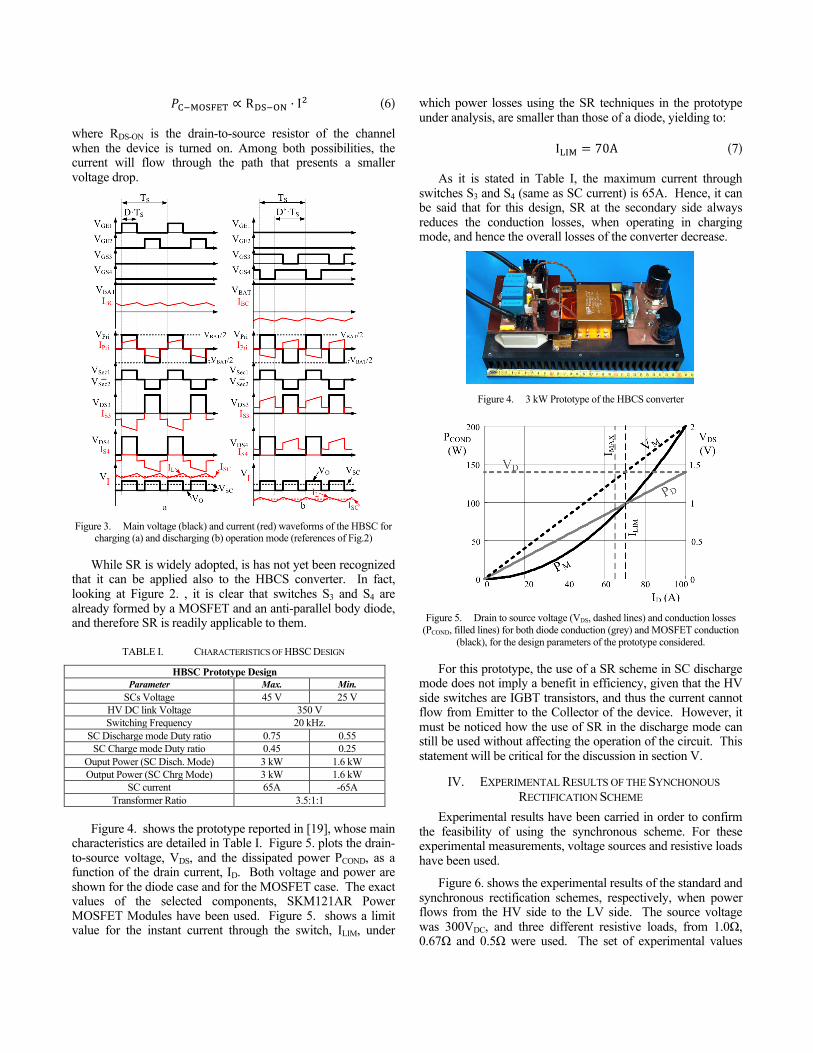
Figure 4. shows the prototype reported in [19], whose main
characteristics are detailed in Table I. Figure 5. plots the drain-to-source voltage, VDS, and the dissipated power PCOND, as a function of the drain current, ID. Both voltage and power are shown for the diode case and for the MOSFET case. The exact values of the selected components, SKM121AR Power MOSFET Modules have been used. Figure 5. shows a limit value for the instant current through the switch, ILIM, under
which power losses using the SR techniques in the prototype under analysis, are smaller than those of a diode, yielding to:
I!"# = 70A (7)
As it is stated in Table I, the maximum current through switches S3 and S4 (same as SC current) is 65A. Hence, it can be said that for this design, SR at the secondary side always reduces the conduction losses, when operating in charging mode, and hence the overall losses of the converter decrease.
Figure 4. 3 kW Prototype of the HBCS converter
Figure 5. Drain to source voltage (VDS, dashed lines) and conduction losses
(PCOND, filled lines) for both diode conduction (grey) and MOSFET conduction (black), for the design parameters of the prototype considered.
For this prototype, the use of a SR scheme in SC discharge mode does not imply a benefit in efficiency, given that the HV side switches are IGBT transistors, and thus the current cannot flow from Emitter to the Collector of the device. However, it must be noticed how the use of SR in the discharge mode can still be used without affecting the operation of the circuit. This statement will be critical for the discussion in section V.
IV. EXPERIMENTAL RESULTS OF THE SYNCHONOUS RECTIFICATION SCHEME
Experimental results have been carried in order to confirm the feasibility of using the synchronous scheme. For these experimental measurements, voltage sources and resistive loads have been used.
Figure 6. shows the experimental results of the standard and synchronous rectification schemes, respectively, when power flows from the HV side to the LV side. The source voltage was 300VDC, and three different resistive loads, from 1.0Ω, 0.67Ω and 0.5Ω were used. The set of experimental values

was measured at VSC=25V, VSC=30V and VSC=34V because of the constraints in the experimental setup. It can be seen how a gain in the efficiency is achieved, slightly below 1%, in all cases.
V. IMPLICATIONS OF SYNCHRONOUS RECTIFICATION IN THE CONTROL SCHEME
The previously proposed modulation scheme needs calculation of two different duty-cycles, according to the power flow, charging or discharging the SCs. In turn, this implies control issues at the boundary from charge to discharge operation, because different switches must be turned on and the control law has to be changed, making it very difficult to have a smooth transition. It will be shown here that this problem is easily overcome if a SR modulation scheme is adopted for both HV and LV side switches.
Figure 6. Graphical relationship of experimental efficiency measurements
between standard and syncrhonous rectification switching schemes, as a fucntion of load resistance. a) VSC=25V. b) VSC=30V. c) VSC=34V
In fact, provided that SR is used, then the HV and LV side switches, S1-S2 and S3-S4 respectively, will have complementary control signals. Particularly, considering the waveforms at Figure 3. .a and b, it can be seen how the control waveform of S4 is the complementary signal of S1, whereas the control waveform of S3 is the complementary signal of S2.
Obviously, this condition implies that there is a relation between the duty cycle D of switches S1-S2 and the duty cycle D’ of S3-S4. This relationship can be expressed as:
𝐷 = 1 − 𝐷′ (8)
and thus there is a single control parameter for all operation modes (e.g. D), as the rest of the control parameters are automatically calculated.
But ((8)), along with ((2)) and ((4)), yield to a single equation for the voltage ratio of the converter, GHBCS, valid for any operation mode, independently of the current direction:
G!"#$ =!!"!!"#
= D · !!!!
(9)
This conclusion implies that the control system can be a single one, thus avoiding the apparent boundary control issue between charging and discharging mode.
VI. FULL MODEL OF THE CONVERTER In order to properly design the control system, an accurate
small signal model of the converter needs to be established. The simplest model for the power stage is depicted in Figure 7. This model has been previously used to define and implement a control strategy for the full system [23]. In such a model, all the switches and reactive components are considered as ideal elements. The switches and the transformer have been substituted by the two dependant sources, which are a function of both the duty ratio and the turns-ratio of the transformer. After that, the LC filter is present.
Figure 7. Model based on ideal components
In order to check the model, a resistive load has been placed instead of the SCs, aiming at having steady state operation conditions. A small step in the duty ratio (changing from 0.34 to 0.36) has been applied to the system once it reached the steady state, in order to characterize the system. Figure 8. shows the experimental waveforms of the inductor current (IL), the input (IBC) and output (ISC) currents, as well as the load output voltage (VSC), compared with their corresponding averaged values coming from the model based on ideal components. As it can be seen, the model is significantly different from the real converter. The natural frequency is quite similar, but basically there are two effects of mismatch: the steady state values are higher in the model than in the real converter and, also, the actual system is much more damped than the model.
A second model has therefore to be introduced, which takes into account the effect of the snubbers, the effect of the RDS of the switches at the secondary side, as well as the effect of the parasitic resistors of the transformer. The combined effect of these components yields to a series resistor, Rloss, which adds a damping factor to the model. But also, the leakage inductance of the transformer has to be taken into account (Figure 9. . In order to explain the effect of this leakage inductor, some

waveforms are depicted in Figure 10. It must be noticed that, for this analysis, the considered resulting leakage inductance at the primary side is the sum of the primary and the secondary side (referred to the primary side) leakage inductances of the transformer.
Initially, both switches at the primary side are turned off, and there is no current through the primary side, but current is flowing through both diodes at the secondary side. At instant t0, switch S1 turns on, and thus the voltage at the primary side of the transformer, Vpri, equals to half the battery voltage:
𝑉!"# =!!"#!
(10)
The high inductor value at the filter, L, forces the current to keep on flowing through L. For the ideal transformer without leakage inductance (Figure 10. a), the current can instantly be conducted by the primary side transistor, thus turning off the diodes of S3 and S4, and hence the voltage at the secondary side instantly equals to:
𝑉!"#! = 𝑉!"#! =!!"#!· !!!!
(11)
Figure 8. Experimental waveforms (black) and averaged value of model
based in ideal components (blue), for filter current (IL), load output current (ISC), load voltage (VSC) and input current (IBC).
However, if there is a leakage inductor at the primary side, as depicted in Figure 9. , the current cannot change instantly (Figure 10. b) at the primary side of the transformer. Thus, current keeps flowing through the secondary side, while S3 and S4 keep on conducting. Hence, the voltage at the secondary side is still zero just after turn on of HV side switches, and the primary side voltage is fully applied to the leakage inductor.
The full effect of this leakage inductor is explained in the following discussion. Here charging mode is considered and initially both HV side switches, S1 and S2, are in off-state, just before S1 is turned on. From Figure 2. and 3.a, upon these conditions, each secondary side will carry a current equal to half the inductor current through the body diodes, the voltage both at the primary side, VPri, and at the common node of the secondary windings (connected to the inductor filter), VO, will be equal to zero:
I!" = I!" = − !!(!)!= − !!
! (12)
V! = 0 (13)
V!"# = 0 (14)
Equation ((12) also states that during the switching interval, the inductor current can be considered as constant.
Figure 9. Equivalent circuit of the transformer including the leakage inductor
of the transformer.
When S1 turns on, at t0, and provided that both the body diodes of S3 and S4 initially keep on conducting, the voltage at the primary side of the ideal transformer, VPri, remains unchanged.
On the other hand, as VDS1 equals to zero, then the voltage at the primary side of the ideal transformer (including the leakage inductance), VPriLk, equals to half the input voltage:
V!"#$% =!!"#!
(15)
This yields to a voltage across the leakage inductor, VLk, and a primary side current, ILK, respectively, equal to:
V!" =!!"#!
(16)
I!" = I!"# =!!!"
!!"#!
· 𝑡 (17)

It must be noticed that this inductor LLk takes into account both the measured leakage inductor at the primary (LLkPri) and secondary (LLkSec) sides of the transformer, as given by the following expression:
L!" = L!"#$% +!!"#$%
!!!!!
!· (18)
Figure 10. a) Switching waveforms with ideal transformer. b) Switching
waveforms with leakage inductor at the primary side
The inductor LLk charges linearly. The currents at the secondary switches can be represented by:
I!" = − !!!− !!"#
!!!!!
(19)
I!" = − !!!+ !!"#
!!!!!
(20)
At instant t1, IS4 equals to zero, and thus S4 turns off. From that moment, the current through the body diode of S3 equals the current through the inductor:
I!" = −𝐼! (21)
I!" = 0 (22)
Thus, the dead time, td, can be defined considering that at instant t1, the current through S3 must be equal to -IL:
− !! !!− !
!· !!!!· !!"#
!· !!!"
t! − t! = −𝐼! 𝑡 (23)
The explicit expression for td can be obtained:
t! = t! − t! =!!!!
!! !!!"#
· 𝐿!" · 2 (24)
It must be noticed that this dead time is an interval of mismatch between the voltage at VO being equal to half of the battery voltage referred to the secondary side at the ideal model, and VO being zero in the full model. The effect of this mismatch is that the effective duty ratio, D1eff, that determines the voltage ratio, is smaller for the latter case. In fact, the effective duty cycle of the system can be expressed as:
D!"## =!!·!!!!!
!! (25)
Provided that the dead time expression depends on input and output parameters, it can be seen how the final expression of D1eff is not a linear expression. This yields to a non-linear model for the behaviour of the system.
Figure 11. depicts the implementation of this model. As stated previously, in addition to the effect of the leakage inductance, a series resistor, Rloss, has been included in order to model the parasitic elements such as series resistors in the transformer windings, conduction and switching losses in the switches, and losses in the snubbers.
In order to validate the new model, a comparison between simulations with this new model has been carried out with the same experimental results for the operating conditions used in Figure 10. The results of this simulation, plotted in Figure 12. , show how the new complete model tracks perfectly the actual prototype waveforms measured, for a duty step from 0.34 to 0.36. The simulation shows the same damped behaviour than the actual waveforms. Thus, it can be concluded that this full model is highly representative of the dynamic small signal behaviour of the HBCS converter.
Figure 11. Full Averaged Model based on real components, parasitic elements
and snubbers
It must be noticed how, for both the ideal and the full models, the obtained behaviour is the corresponding to a 2nd order system, as expected from a resistive load at the output. Instead, if the SCs are connected at the output without the resistor, the output voltage would present a practically constant value at the transient, but would charge/discharge with the corresponding current.
VII. PROPOSED CONTROL SCHEME For the Converter Control System, a cascaded loop control
scheme is proposed. A High Level Control system provides the reference for the HV current value of the HBCS converter, IBC
*, as depicted in Figure 13. Figure 14. shows a detail of the implementation of the IBC control. The inner control loop controls the inductor filter current, IL, and the outer control loop controls the HV side current, IBC. It must be noticed how in steady state, and for adequate values of the filter capacitor, C, the average value of IL equals the average value of ISC. A detailed explanation on the control loop design procedure and on the PI controllers tuning can be seen in [23].
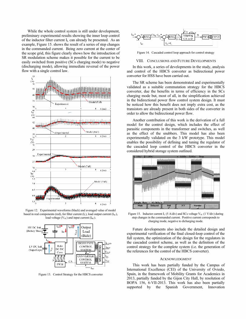
While the whole control system is still under development, preliminary experimental results showing the inner loop control of the inductor filter current IL can already be presented. As an example, Figure 15. shows the result of a series of step changes in the commanded current. Being zero current at the center of the scope grid, this figure clearly shows how the introduction of SR modulation scheme makes it possible for the current to be easily switched from positive (SCs charging mode) to negative (discharging mode), allowing immediate reversal of the power flow with a single control law.
Figure 12. Experimental waveforms (black) and averaged value of model
based in real components (red), for filter current (IL), load output current (ISC), load voltage (VSC) and input current (IBC).
Figure 13. Control Strategy for the HBCS converter
Figure 14. Cascaded control loop approach for control strategy
VIII. CONCLUSIONS AND FUTURE DEVELOPMENTS In this work, a series of developments in the study, analysis
and control of the HBCS converter as bidirectional power converter for HSS have been carried out.
The SR scheme has been demonstrated and experimentally validated as a suitable commutation strategy for the HBCS converter, due the benefits in terms of efficiency in the SCs charging mode but, most of all, in the simplification achieved in the bidirectional power flow control system design. It must be noticed how this benefit does not imply extra cost, as the transistors are already present in both sides of the converter in order to allow the bidirectional power flow.
Another contribution of this work is the derivation of a full model for the control design, which includes the effect of parasitic components in the transformer and switches, as well as the effect of the snubbers. This model has also been experimentally validated on the 3 kW prototype. This model enables the possibility of defining and tuning the regulator of the cascaded loop control of the HBCS converter in the considered hybrid storage system outlined.
Figure 15. Inductor current IL (5 A/div) and SCs voltage VSC (1 V/div) during
step changes in the commanded current. Positive current corresponds to charging mode, negative to dicharging mode.
Future developments also include the detailed design and experimental verification of the final closed-loop control of the full system, the optimization of the design for the regulators in the cascaded control scheme, as well as the definition of the control strategy for the complete system (i.e. the generation of the references for the control of the HBCS converter).
ACKNOWLEDGMENT This work has been partially funded by the Campus of
International Excellence (CEI) of the University of Oviedo, Spain, in the framework of Mobility Grants for Academics in 2013, partially funded by the Gijon City Hall, by resolution of BOPA 156, 6-VII-2013. This work has also been partially supported by the Spanish Government, Innovation

Development and Research Office (MEC), under research grant ENE2013-44245-R, Project “Microholo”, and by the European Union through ERFD Structural Funds (FEDER).
REFERENCES [1] Ostadi, A.; Kazerani, M.; Shih-Ken Chen, "Hybrid Energy Storage
System (HESS) in vehicular applications: A review on interfacing battery and ultra-capacitor units," Transportation Electrification Conference and Expo (ITEC), 2013 IEEE , vol., no., pp.1,7, 16-19 June 2013, doi: 10.1109/ITEC.2013.6573471
[2] Amjadi, Z.; Williamson, S.S., "Digital Control of a Bidirectional DC/DC Switched Capacitor Converter for Hybrid Electric Vehicle Energy Storage System Applications," Smart Grid, IEEE Transactions on , vol.5, no.1, pp.158,166, Jan. 2014, doi: 10.1109/TSG.2013.2264489
[3] Kuperman, A.; Mellincovsky, M.; Lerman, C.; Aharon, I.; Reichbach, N.; Geula, G.; Nakash, R., "Supercapacitor Sizing Based on Desired Power and Energy Performance," Power Electronics, IEEE Transactions on , vol.29, no.10, pp.5399,5405, Oct. 2014, doi: 10.1109/TPEL.2013.2292674
[4] Cohen, I.J.; Kelley, J.P.; Wetz, D.A.; Heinzel, J., "Evaluation of a Hybrid Energy Storage Module for Pulsed Power Applications," Plasma Science, IEEE Transactions on , vol.PP, no.99, pp.1,1. doi: 10.1109/TPS.2014.2298369
[5] Farooque M., Maru H.C., “Fuel cells-the clean and efficient power generators”, Proceedings of the IEEE, vol. 89, issue 12, Dec. 2001, pp. 1819-1829.
[6] Di Napoli, A, Caricchi, F., Crescimbini, F. “Ultracapacitor based bidirectional DC-DC converter prototype for recovery of the braking energy in EV motor drives”, 6th European Conf. on Power Electronics and Applications (EPE’95), Sevilla (Spain), September 1995.
[7] Mestre, P., Astier, S., “Application of supercapacitors and influence of the drive control strategies on the performances of on electric vehicle”, 15th Electric Vehicle Symposium (EVS-15), Bruxelles (Belgium), October 1998.
[8] Barra, G.P., Genova, P.A., Morhet, P., Brusaglino, G.P., Rena, P., “Supercapacitors for EV, results, trends and industrial perspectives”, 13th Electric Vehicle Symposium (EVS-13), Osaka (Japan), October 1996.
[9] Takehara J., Miyaoka K., Fukuda T., “EV Mini-Van Featuring Series Conjunction of Ultracapacitors and Batteries for Load Leveling of its Batteries”, 15th Electric Vehicle Symposium (EVS-15), Bruxelles (Belgium), October 1998.
[10] Schmid M., “Electric Double-Layer Capacitor in a Hybrid Vehicle - Basic Considerations and Simulation Results”, 13th Electric Vehicle Symposium (EVS-13), Osaka (Japan), October 1996.
[11] King, R.d., Schwartz, J., Cardinal, M., Garrigan, L.S “Development and system test of high efficiency ultracapacitor/battery electronic interface”, 15th Electric Vehicle Symposium (EVS-15), Bruxelles (Belgium), October 1998.
[12] Caricchi, F., Crescimbini, F., Di Napoli, A., Giulii Capponi, F. Solero, L., ‘Multiple input DC-DC power converter for power flow management in hybrid vehicles’, 37th IEEE Industry Applications Society Annual
Meeting (IAS’02), October 13-17, 2002, Pittsburgh, PA, USA, pp. 1578-1585.
[13] Di Napoli, A., Giulii Capponi, F., Solero, L., “Power Converter Arrangements with Ultracapacitor Tank for Battery Load Leveling in EV Motor Drives” 8th European Conf. on Power Electronics and Applications (EPE’99), Lausanne (Switzerland), 7-9 September 1999.
[14] Brucchi, F., Lo Bianco, G., Salvati, P., Giulii Capponi, F., Solero, L., “Employment of Ultra-capacitors for Power Levelling Requirements in EV: a State of the Art” Proc. of 32nd International Symposium on Automotive Technology and Automation (ISATA’99), Vienna (Austria), 14-18 June 1999.
[15] Jain, M., Daniele, M., Jain, P.K., “A bidirectional DC-DC converter topology for low power application” IEEE Transactions on Power Electronics, Vol. 15, n. 4, July 2000, pp. 595 – 606.
[16] Kazimierczuk, M.K., Vuong, D.Q., Nguyen, B.T., Weimer, J.A., ‘Topologies of bidirectional PWM dc-dc power converters’, IEEE 1993 National Aerospace and Electronics Conference (NAECON’93), 24-28 May 1993, pp. 435 – 441.
[17] Giulii Capponi, F., Cacciato, M., "Using Super Capacitors in Combination with Bi-Directional DC/DC Converters for Active Load Management in Residential Fuel Cell Applications”, 1st European Symposium on Supercapacitors (ESSCAP’04), Belfort (France), 4-5 November 2004.
[18] Cacciato, M.; Caricchi, F.; Giuhlii, F.; Santini, E., "A critical evaluation and design of bi-directional DC/DC converters for super-capacitors interfacing in fuel cell applications,"Industry Applications Conference, 2004. 39th IAS Annual Meeting. Conference Record of the 2004 IEEE , vol.2, no., pp.1127,1133 vol.2, 3-7 Oct. 2004, doi: 10.1109/IAS.2004.1348554
[19] Giulii Capponi, F., Santoro, P.; Crescenzi, E., "HBCS Converter: A Bidirectional DC/DC Converter for Optimal Power Flow Regulation in Supercapacitor Applications," Industry Applications Conference, 2007. 42nd IAS Annual Meeting. Conference Record of the 2007 IEEE , vol., no., pp.2009,2015, 23-27 Sept. 2007.
[20] Yingchao, Z., Zhen, G., Yongchang, Z., Tianwen, Z., Liping, J., "Active battery/ultracapacitor hybrid energy storage system based on soft-switching bidirectional converter," Electrical Machines and Systems (ICEMS), 2013 International Conference on , vol., no., pp.2177,2182, 26-29 Oct. 2013. doi: 10.1109/ICEMS.2013.6713198
[21] Wai, R.J., Duan, R.Y., "High-Efficiency Bidirectional Converter for Power Sources With Great Voltage Diversity," Power Electronics, IEEE Transactions on , vol.22, no.5, pp.1986,1996, Sept. 2007. doi: 10.1109/TPEL.2007.904167
[22] Yamamoto, K.; Hiraki, E.; Tanaka, T.; Nakaoka, M.; Mishima, T., "Bidirectional DC-DC Converter with Full-bridge / Push-pull circuit for Automobile Electric Power Systems," Power Electronics Specialists Conference, 2006. PESC '06. 37th IEEE , vol., no., pp.1,5, 18-22 June 2006. doi: 10.1109/PESC.2006.1711776
[23] Garcia, J.; Capponi, F.G.; Borocci, G., Garcia, P. “Control Strategy for Bidirectional HBCS Converter with for Super capacitor Applications”, , IEEE-ISIE 2014 The 23rd IEEE International Symposium on Industrial Electronics 1-4 June 2014, Istanbul, TURKEY