ANALYSIS AND SIMULATION OF BUS-CLAMPING … space vector pulse width modulation employs conventional...
10
M.THANUJA* et al. ISSN: 2250–3676 [IJESAT] INTERNATIONAL JOURNAL OF ENGINEERING SCIENCE & ADVANCED TECHNOLOGY Volume - 2, Issue - 1, 64 – 73 IJESAT | Jan-Feb 2012 Available online @ http://www.ijesat.org 64 ANALYSIS AND SIMULATION OF BUS-CLAMPING PWM TECHNIQUES BASED ON SPACE VECTOR APPROACH Ms.M.Thanuja 1 , Mrs.B.Jyothi 2 , Dr.M.Venugopal Rao 3 1 Asst.professor, EEE dept, G .pullaiah College of Engineering, Andhra Pradesh, India , [email protected] 2 Asst.Professor, EEE dept, K.L.University, Andhra Pradesh , India , [email protected] 3 Professor, HOD of EEE , K .L University , Andhra Pradesh, India, venumannam @ gmail.com Abstract Conventional space vector pulse width modulation employs conventional switching sequence, which divides the zero vector time equally between the two zero states in every sub cycle .Existing bus-clamping PWM techniques employ clamping sequences, which use only one zero state in a sub cycle. In the present work a new set of BCPWM dealing with a special type of switching sequences, termed as “double-switching clamping sequences”, which use only one zero state and an active vector repeats twice in a sub cycle, will be proposed. It is shown analytically that the proposed BCPWM techniques result in reduced harmonic distortion in the line currents over CSVPWM as well as existing BCPWM techniques at high modulation indices for given a average switching frequency. This work deals with Analysis and Simulation of “double-switching clamping sequences” in terms of stator flux ripple and line current harmonic distortion. Simulation is done on v/f controlled Induction Motor drive in MATLAB/SIMULINK environment Index Terms: Bus clamping pulse width modulation (BCPWM),discontinuous PWM, harmonic distortion, induction, motor drives ,PWM inverters, space vector PWM, stator flux ripple, switching sequences. --------------------------------------------------------------------- *** ------------------------------------------------------------------------ 1. INTRODUCTION Voltage source inverter fed induction motors are widely used in variable speed applications. The harmonic distortion in the motor phase currents must be low for satisfactory operation of the motor drive. The harmonic distortion in the current is determined by the switching frequency and PWM Technique is employed. The switching frequency cannot be increased beyond a certain range due to practical limitations. The distortion is reduced at a given switching frequency by a good design of PWM Technique. This project focuses on developing and evaluating new real time PWM techniques for voltage source inverters. SPWM and CSVPWM are very popular real time techniques. CSVPWM and THIPWM lead to higher line side voltages for given dc bus voltage compare to SPWM. These technique results in less harmonic distortion in motor currents than SPWM at a given line voltage. Discontinuous modulation methods lead to reduction in distortion at higher line voltages over a CSVPWM for a given average switching frequency. This paper proposes high performance HSVPWM, which further reduce the distortion in the line currents over comparable real-time technique at a given average switching frequency. The superiority in performance of proposed techniques is established theoretically as well as experimentally. With SPWM, CSVPWM and THIPWM, every phase switches once in a sub-cycle or half carrier signal. This paper explores novel switching sequence that switch ‗a‘ phase twice in a sub- cycle, while switching second phase once and clamping the third phase. This paper brings out all such possible sequences (including two new sequences), which results same average switching frequency as CSVPWM for a given sampling frequency. The proposed hybrid PWM techniques employ the sequence which results in the lowest rms current ripples over given sub cycle, out of given set of sequences. Consequently the total rms current ripple over fundamental cycle is reduced
Transcript of ANALYSIS AND SIMULATION OF BUS-CLAMPING … space vector pulse width modulation employs conventional...
M.THANUJA* et al. ISSN: 2250–3676
[IJESAT] INTERNATIONAL JOURNAL OF ENGINEERING SCIENCE & ADVANCED TECHNOLOGY Volume - 2, Issue - 1, 64 – 73
IJESAT | Jan-Feb 2012
Available online @ http://www.ijesat.org 64
ANALYSIS AND SIMULATION OF BUS-CLAMPING PWM TECHNIQUES
BASED ON SPACE VECTOR APPROACH
Ms.M.Thanuja1, Mrs.B.Jyothi
2 , Dr.M.Venugopal Rao
3
1 Asst.professor, EEE dept, G .pullaiah College of Engineering, Andhra Pradesh, India , [email protected]
2 Asst.Professor, EEE dept, K.L.University, Andhra Pradesh , India , [email protected]
3 Professor, HOD of EEE , K .L University , Andhra Pradesh, India, venumannam @ gmail.com
Abstract Conventional space vector pulse width modulation employs conventional switching sequence, which divides the zero vector time
equally between the two zero states in every sub cycle .Existing bus-clamping PWM techniques employ clamping sequences, which use
only one zero state in a sub cycle. In the present work a new set of BCPWM dealing with a special type of switching sequences, termed
as “double-switching clamping sequences”, which use only one zero state and an active vector repeats twice in a sub cycle, will be
proposed.
It is shown analytically that the proposed BCPWM techniques result in reduced harmonic distortion in the line currents over
CSVPWM as well as existing BCPWM techniques at high modulation indices for given a average switching frequency. This work
deals with Analysis and Simulation of “double-switching clamping sequences” in terms of stator flux ripple and line current harmonic
distortion. Simulation is done on v/f controlled Induction Motor drive in MATLAB/SIMULINK environment
Index Terms: Bus clamping pulse width modulation (BCPWM),discontinuous PWM, harmonic distortion, induction,
motor drives ,PWM inverters, space vector PWM, stator flux ripple, switching sequences.
--------------------------------------------------------------------- *** ------------------------------------------------------------------------
1. INTRODUCTION
Voltage source inverter fed induction motors are widely used
in variable speed applications. The harmonic distortion in the
motor phase currents must be low for satisfactory operation of
the motor drive. The harmonic distortion in the current is
determined by the switching frequency and PWM Technique
is employed. The switching frequency cannot be increased
beyond a certain range due to practical limitations. The
distortion is reduced at a given switching frequency by a good
design of PWM Technique. This project focuses on
developing and evaluating new real time PWM techniques for
voltage source inverters.
SPWM and CSVPWM are very popular real time techniques.
CSVPWM and THIPWM lead to higher line side voltages for
given dc bus voltage compare to SPWM. These technique
results in less harmonic distortion in motor currents than
SPWM at a given line voltage. Discontinuous modulation
methods lead to reduction in distortion at higher line voltages
over a CSVPWM for a given average switching frequency.
This paper proposes high performance HSVPWM, which
further reduce the distortion in the line currents over
comparable real-time technique at a given average switching
frequency. The superiority in performance of proposed
techniques is established theoretically as well as
experimentally.
With SPWM, CSVPWM and THIPWM, every phase switches
once in a sub-cycle or half carrier signal. This paper explores
novel switching sequence that switch ‗a‘ phase twice in a sub-
cycle, while switching second phase once and clamping the
third phase. This paper brings out all such possible sequences
(including two new sequences), which results same average
switching frequency as CSVPWM for a given sampling
frequency.
The proposed hybrid PWM techniques employ the sequence
which results in the lowest rms current ripples over given sub
cycle, out of given set of sequences. Consequently the total
rms current ripple over fundamental cycle is reduced
M.THANUJA* et al. ISSN: 2250–3676
[IJESAT] INTERNATIONAL JOURNAL OF ENGINEERING SCIENCE & ADVANCED TECHNOLOGY Volume - 2, Issue - 1, 64 – 73
IJESAT | Jan-Feb 2012
Available online @ http://www.ijesat.org 65
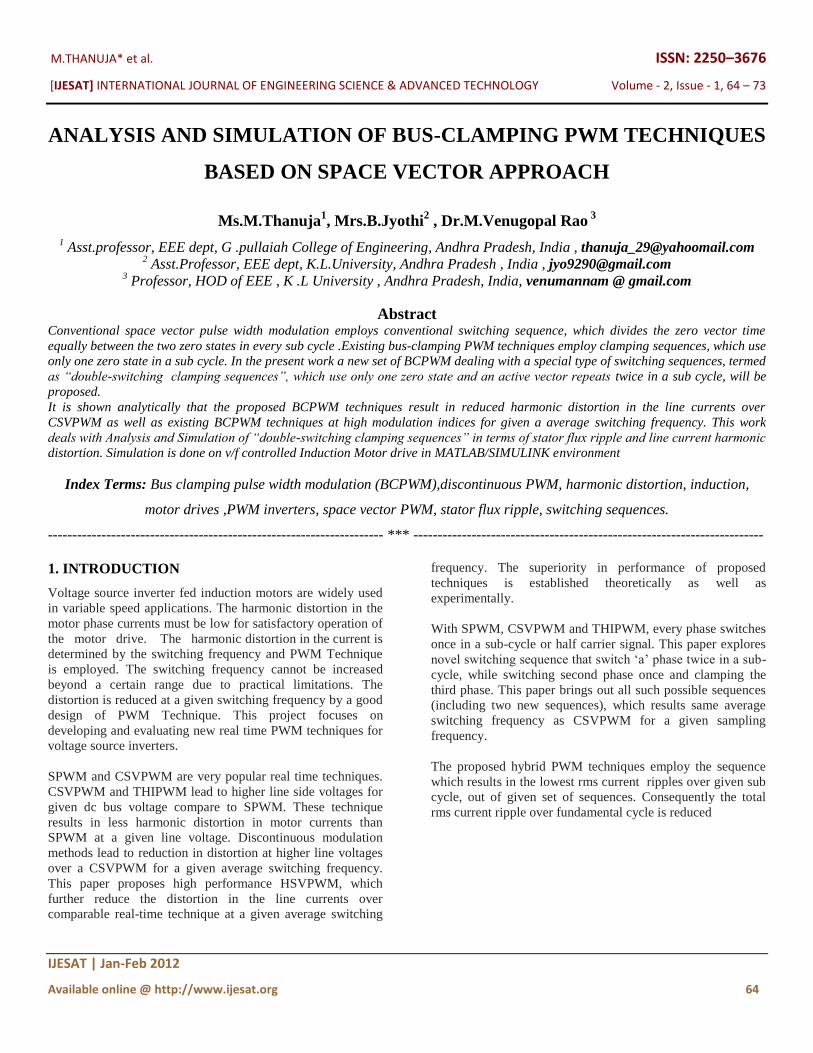
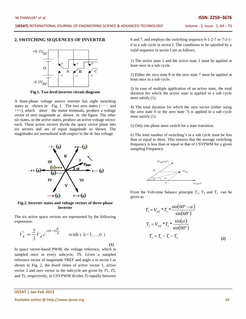
2. SWITCHING SEQUENCES OF INVERTER
Fig.1. Two level inverter circuit diagram
A three-phase voltage source inverter has eight switching
states as shown in Fig. 1. The two zero states (−−− and
+++), which short the motor terminals, produce a voltage
vector of zero magnitude as shown in the figure. The other
six states, or the active states, produce an active voltage vector
each. These active vectors divide the space vector plane into
six sectors and are of equal magnitude as shown. The
magnitudes are normalized with respect to the dc bus voltage.
Fig.2. Inverter states and voltage vectors of three-phase
Inverter
The six active space vectors are represented by the following
expression:
(1)
In space vector-based PWM, the voltage reference, which is
sampled once in every subcycle, TS. Given a sampled
reference vector of magnitude VREF and angle α in sector I as
shown in Fig. 2, the dwell times of active vector 1, active
vector 2 and zero vector in the subcycle are given by T1, T2,
and TZ, respectively, in CSVPWM divides TZ equally between
0 and 7, and employs the switching sequence 0-1-2-7 or 7-2-1-
0 in a sub cycle in sector I. The conditions to be satisfied by a
valid sequence in sector I are as follows.
1) The active state 1 and the active state 2 must be applied at
least once in a sub cycle.
2) Either the zero state 0 or the zero state 7 must be applied at
least once in a sub cycle.
3) In case of multiple application of an active state, the total
duration for which the active state is applied in a sub cycle
must satisfy (1).
4) The total duration for which the zero vector (either using
the zero state 0 or the zero state 7) is applied in a sub cycle
must satisfy (1).
5) Only one phase must switch for a state transition.
6) The total number of switching‘s in a sub cycle must be less
than or equal to three. This ensures that the average switching
frequency is less than or equal to that of CSVPWM for a given
sampling Frequency.
From the Volt-time balance principle T1, T2 and Tz can be
given as
(2)
60sin
60sin**1
sref TVT
60sin
sin**2
sref TVT
21 TTTT sz
M.THANUJA* et al. ISSN: 2250–3676
[IJESAT] INTERNATIONAL JOURNAL OF ENGINEERING SCIENCE & ADVANCED TECHNOLOGY Volume - 2, Issue - 1, 64 – 73
IJESAT | Jan-Feb 2012
Available online @ http://www.ijesat.org 66
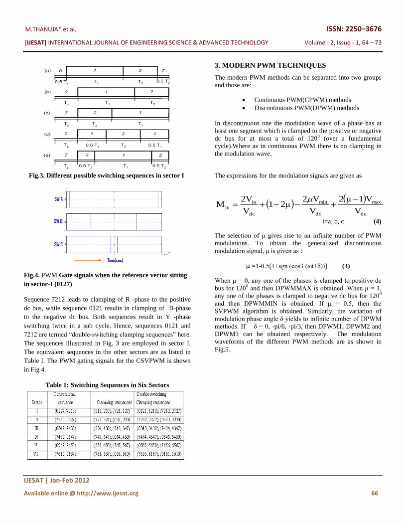
Fig.3. Different possible switching sequences in sector I
Fig.4. PWM Gate signals when the reference vector sitting
in sector-I (0127)
Sequence 7212 leads to clamping of R -phase to the positive
dc bus, while sequence 0121 results in clamping of B-phase
to the negative dc bus. Both sequences result in Y -phase
switching twice in a sub cycle. Hence, sequences 0121 and
7212 are termed ―double-switching clamping sequences‖ here.
The sequences illustrated in Fig. 3 are employed in sector I.
The equivalent sequences in the other sectors are as listed in
Table I. The PWM gating signals for the CSVPWM is shown
in Fig 4.
Table 1: Switching Sequences in Six Sectors
3. MODERN PWM TECHNIQUES
The modern PWM methods can be separated into two groups
and those are:
Continuous PWM(CPWM) methods
Discontinuous PWM(DPWM) methods
In discontinuous one the modulation wave of a phase has at
least one segment which is clamped to the positive or negative
dc bus for at most a total of 1200 (over a fundamental
cycle).Where as in continuous PWM there is no clamping in
the modulation wave.
The expressions for the modulation signals are given as
dc
max
dc
min
dc
inin
V
V1μ2
V
V22μ1
V
2VM
i=a, b, c (4)
The selection of μ gives rise to an infinite number of PWM
modulations. To obtain the generalized discontinuous
modulation signal, μ is given as :
μ =1-0.5[1+sgn (cos3 (ωt+δ))] (3)
When μ = 0, any one of the phases is clamped to positive dc
bus for 1200 and then DPWMMAX is obtained. When μ = 1,
any one of the phases is clamped to negative dc bus for 1200
and then DPWMMIN is obtained. If μ = 0.5, then the
SVPWM algorithm is obtained. Similarly, the variation of
modulation phase angle δ yields to infinite number of DPWM
methods. If δ = 0, -pi/6, -pi/3, then DPWM1, DPWM2 and
DPWM3 can be obtained respectively. The modulation
waveforms of the different PWM methods are as shown in
Fig.5.
M.THANUJA* et al. ISSN: 2250–3676
[IJESAT] INTERNATIONAL JOURNAL OF ENGINEERING SCIENCE & ADVANCED TECHNOLOGY Volume - 2, Issue - 1, 64 – 73
IJESAT | Jan-Feb 2012
Available online @ http://www.ijesat.org 67
Fig.5.Modulation waveforms of the various PWM methods
The conventional SVPWM algorithm employs equal division
of zero voltage vector times within a sampling period or sub
cycle. However, by utilizing the freedom of zero state
division, various DPWM methods can be generated. GDPWM algorithm, which uses the utilization of the freedom
of zero state time division. In this proposed method the zero
state time will be shared between two zero states as T0 for V0
and T7 for V7 respectively, and T0 , T7 can be expressed as:
(5)
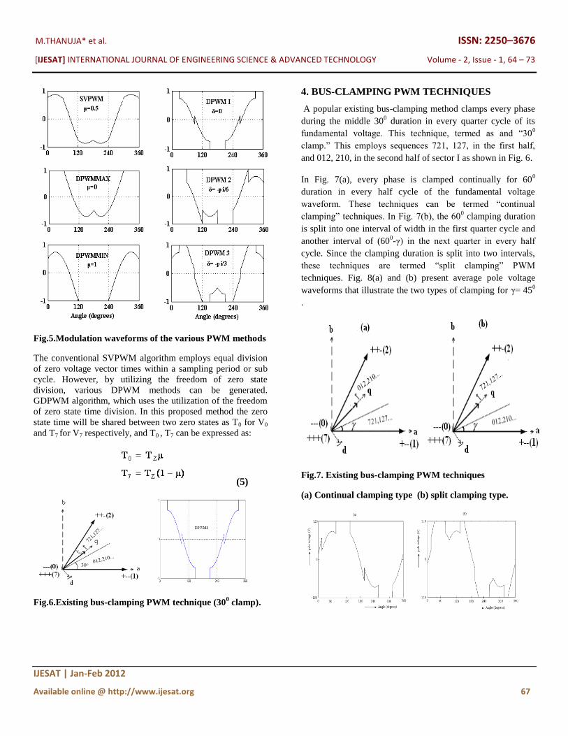
Fig.6.Existing bus-clamping PWM technique (300 clamp).
4. BUS-CLAMPING PWM TECHNIQUES
A popular existing bus-clamping method clamps every phase
during the middle 300 duration in every quarter cycle of its
fundamental voltage. This technique, termed as and ―300
clamp.‖ This employs sequences 721, 127, in the first half,
and 012, 210, in the second half of sector I as shown in Fig. 6.
In Fig. 7(a), every phase is clamped continually for 600
duration in every half cycle of the fundamental voltage
waveform. These techniques can be termed ―continual
clamping‖ techniques. In Fig. 7(b), the 600 clamping duration
is split into one interval of width in the first quarter cycle and
another interval of (600-γ) in the next quarter in every half
cycle. Since the clamping duration is split into two intervals,
these techniques are termed ―split clamping‖ PWM
techniques. Fig. 8(a) and (b) present average pole voltage
waveforms that illustrate the two types of clamping for γ= 450
.
Fig.7. Existing bus-clamping PWM techniques
(a) Continual clamping type (b) split clamping type.
M.THANUJA* et al. ISSN: 2250–3676
[IJESAT] INTERNATIONAL JOURNAL OF ENGINEERING SCIENCE & ADVANCED TECHNOLOGY Volume - 2, Issue - 1, 64 – 73
IJESAT | Jan-Feb 2012
Available online @ http://www.ijesat.org 68
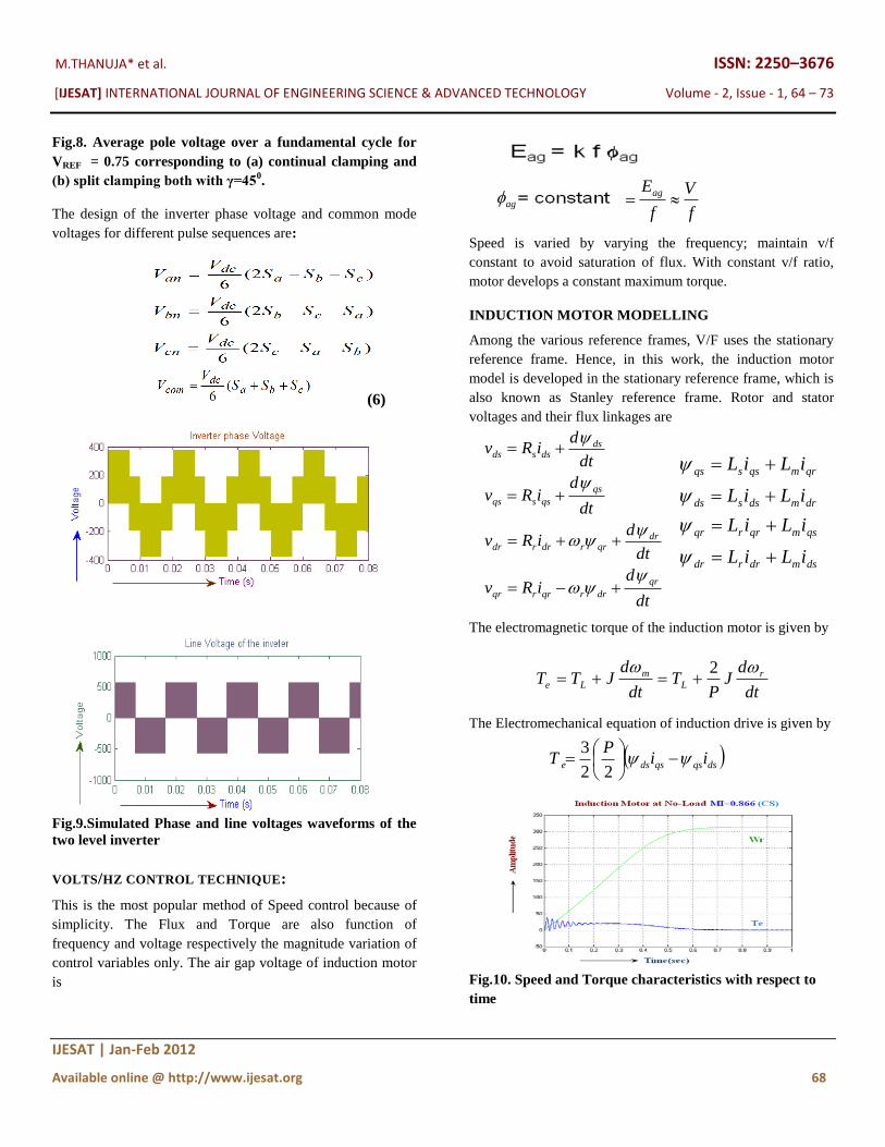
Fig.8. Average pole voltage over a fundamental cycle for
VREF = 0.75 corresponding to (a) continual clamping and
(b) split clamping both with γ=450.
The design of the inverter phase voltage and common mode
voltages for different pulse sequences are:
(6)
Fig.9.Simulated Phase and line voltages waveforms of the
two level inverter
VOLTS/HZ CONTROL TECHNIQUE:
This is the most popular method of Speed control because of
simplicity. The Flux and Torque are also function of
frequency and voltage respectively the magnitude variation of
control variables only. The air gap voltage of induction motor
is
Speed is varied by varying the frequency; maintain v/f
constant to avoid saturation of flux. With constant v/f ratio,
motor develops a constant maximum torque.
INDUCTION MOTOR MODELLING
Among the various reference frames, V/F uses the stationary
reference frame. Hence, in this work, the induction motor
model is developed in the stationary reference frame, which is
also known as Stanley reference frame. Rotor and stator
voltages and their flux linkages are
The electromagnetic torque of the induction motor is given by
The Electromechanical equation of induction drive is given by
Fig.10. Speed and Torque characteristics with respect to
time
dt
diRv
dt
diRv
dt
diRv
dt
diRv
qr
drrqrrqr
drqrrdrrdr
qs
qssqs
dsdssds
dsmdrrdr
qsmqrrqr
drmdssds
qrmqssqs
iLiL
iLiL
iLiL
iLiL
dsqsqsdse ii
PT
22
3
dt
dJ
PT
dt
dJTT r
L
m
Le
2
agf
V
f
Eag
M.THANUJA* et al. ISSN: 2250–3676
[IJESAT] INTERNATIONAL JOURNAL OF ENGINEERING SCIENCE & ADVANCED TECHNOLOGY Volume - 2, Issue - 1, 64 – 73
IJESAT | Jan-Feb 2012
Available online @ http://www.ijesat.org 69
Fig.11. Block diagram of V/F controlled BCPWM based
IM drive
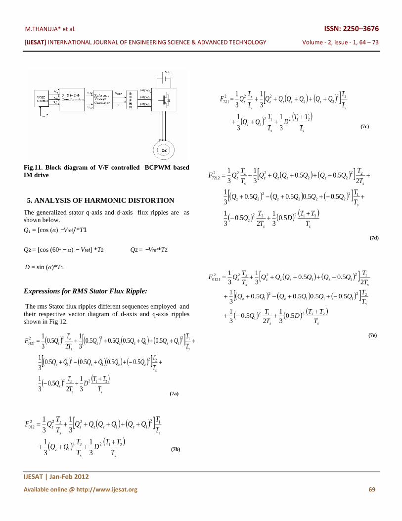
5. ANALYSIS OF HARMONIC DISTORTION
The generalized stator q-axis and d-axis flux ripples are as
shown below.
Q1 = [cos (α) −Vref] *T1
Q2 = [cos (60° − α) − Vref] *T2 QZ = −Vref*TZ
D = sin (α)*T1.
Expressions for RMS Stator Flux Ripple:
The rms Stator flux ripples different sequences employed and
their respective vector diagram of d-axis and q-axis ripples
shown in Fig 12.
(7a)
(7b)
(7c)
(7d)
(7e)
ss
zz
s
zzzz
s
zzzz
s
zz
T
TTD
T
TQ
T
TQQQQQQ
T
TQQQQQQ
T
TQF
2122
22
1
2
1
12
11
222
0127
3
1
25.0
3
1
5.05.05.05.03
1
5.05.05.05.03
1
25.0
3
1
ss
z
s
zzzz
s
zz
T
TTD
T
TQQ
T
TQQQQQQ
T
TQF
21222
1
12
11
222
012
3
1
3
1
3
1
3
1
ss
z
s
zzzz
s
zz
T
TTD
T
TQQ
T
TQQQQQQ
T
TQF
21212
2
22
22
222
721
3
1
3
1
3
1
3
1
ss
s
zz
s
zzzz
s
zz
T
TTD
T
TQ
T
TQQQQQQ
T
TQQQQQQ
T
TQF
21212
1
22
111
2
1
12
11
222
0121
5.03
1
25.0
3
1
5.05.05.05.03
1
25.05.0
3
1
3
1
ss
s
zz
s
zzzz
s
zz
T
TTD
T
TQ
T
TQQQQQQ
T
TQQQQQQ
T
TQF
21222
2
12
222
2
2
22
22
222
7212
5.03
1
25.0
3
1
5.05.05.05.03
1
25.05.0
3
1
3
1
M.THANUJA* et al. ISSN: 2250–3676
[IJESAT] INTERNATIONAL JOURNAL OF ENGINEERING SCIENCE & ADVANCED TECHNOLOGY Volume - 2, Issue - 1, 64 – 73
IJESAT | Jan-Feb 2012
Available online @ http://www.ijesat.org 70
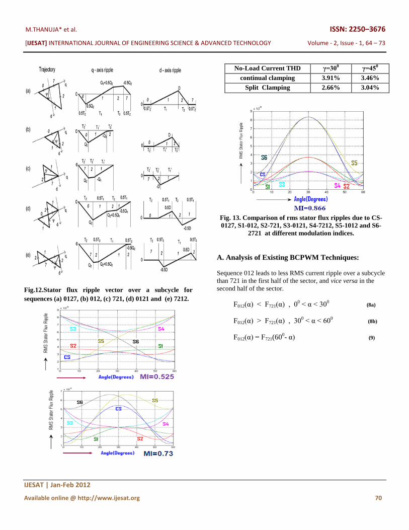
Fig.12.Stator flux ripple vector over a subcycle for
sequences (a) 0127, (b) 012, (c) 721, (d) 0121 and (e) 7212.
Fig. 13. Comparison of rms stator flux ripples due to CS-
0127, S1-012, S2-721, S3-0121, S4-7212, S5-1012 and S6-
2721 at different modulation indices.
A. Analysis of Existing BCPWM Techniques:
Sequence 012 leads to less RMS current ripple over a subcycle
than 721 in the first half of the sector, and vice versa in the
second half of the sector.
F012(α) < F721(α) , 00 < α < 30
0 (8a)
F012(α) > F721(α) , 300 < α < 60
0 (8b)
F012(α) = F721(600- α) (9)
No-Load Current THD γ=300 γ=45
0
continual clamping 3.91% 3.46%
Split Clamping 2.66% 3.04%
M.THANUJA* et al. ISSN: 2250–3676
[IJESAT] INTERNATIONAL JOURNAL OF ENGINEERING SCIENCE & ADVANCED TECHNOLOGY Volume - 2, Issue - 1, 64 – 73
IJESAT | Jan-Feb 2012
Available online @ http://www.ijesat.org 71
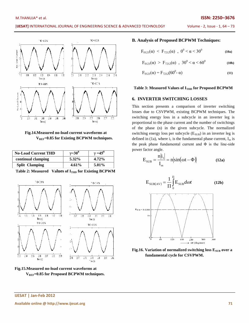
Fig.14.Measured no-load current waveforms at
VREF=0.85 for Existing BCPWM techniques.
Table 2: Measured Values of ITHD for Existing BCPWM
Fig.15.Measured no-load current waveforms at
VREF=0.85 for Proposed BCPWM techniques.
B. Analysis of Proposed BCPWM Techniques:
F0121(α) < F7212(α) , 00 < α < 30
0 (10a)
F0121(α) > F7212(α) , 300 < α < 60
0 (10b)
F0121(α) = F7212(600- α) (11)
Table 3: Measured Values of ITHD for Proposed BCPWM
6. INVERTER SWITCHING LOSSES
This section presents a comparison of inverter switching
losses due to CSVPWM, existing BCPWM techniques. The
switching energy loss in a subcycle in an inverter leg is
proportional to the phase current and the number of switchings
of the phase (n) in the given subcycle. The normalized
switching energy loss per subcycle (ESUB) in an inverter leg is
defined in (1a), where i1 is the fundamental phase current, Im is
the peak phase fundamental current and Φ is the line-side
power factor angle.
ΦωtsinnI
inE
m
1
SUB (12a)
td
Π
0
SUBAVSUB EΠ
1E (12b)
Fig.16. Variation of normalized switching loss ESUB over a
fundamental cycle for CSVPWM.
No-Load Current THD γ=300 γ =45
0
continual clamping 5.32% 4.72%
Split Clamping 4.61% 5.01%

M.THANUJA* et al. ISSN: 2250–3676
[IJESAT] INTERNATIONAL JOURNAL OF ENGINEERING SCIENCE & ADVANCED TECHNOLOGY Volume - 2, Issue - 1, 64 – 73
IJESAT | Jan-Feb 2012
Available online @ http://www.ijesat.org 72
(a) (b)
(c) (d)
Fig. 17. Variation of normalized switching loss ESUB over a
fundamental cycle for Existing BCPWM techniques.
Average Switching Loss for CSVPWM = 0.6366
Table 4: Measured Values of Average Switching Loss
7. CONCLUSION
A class of bus-clamping PWM (BCPWM) techniques, which
employ only the double-switching clamping sequences, is
proposed. The proposed BCPWM techniques are studied, and
are compared against conventional space vector PWM
(CSVPWM) and existing BCPWM techniques at a given
average switching frequency. The proposed families of
BCPWM techniques result in less line current distortion than
CSVPWM and the existing BCPWM techniques at high line
voltages close to the highest line side voltage during linear
modulation. The analysis presented explains the difference in
distortion due to the different techniques. The study classifies
both the existing BCPWM and the proposed BCPWM
techniques into two categories, namely continual clamping
methods and split clamping methods, depending on the type of
clamping adopted. It is shown that split clamping methods are
better than continual clamping ones in terms of line current
distortion. In terms of switching losses, continual clamping is
better at high power factors, while split clamping is superior at
low power factors.
REFERENCES
[1] ―Advanced Bus-Clamping PWM Techniques Based on
Space Vector Approach‖ G. Narayanan, Member, IEEE,
Harish K. Krishnamurthy, Di Zhao, and Rajapandian Ayyanar,
Member, IEEE,2006.
[2] J. Holtz, ―Pulse width modulation—A survey,‖ IEEE
Trans Ind. Electron., vol. 39, no. 5, pp. 410–420, Dec. 1992.
[3] J. Holtz, ―Pulse width modulation for electronic power
conversion,‖ Proc. IEEE, vol. 82, no. 8, pp. 1194–1214, Aug.
1994.
[4] D. G. Holmes and T. A. Lipo, Pulse Width Modulation for
Power Converters: Principle and Practice. New York: Wiley,
2003.
[5] V. Blasko, ―Analysis of a hybrid PWM based on modified
space-vector and triangle-comparison methods,‖ IEEE Trans.
Ind. Appl., vol. 33, no. 3, pp. 756–764, May/Jun. 1997.
[6] D. Zhao, G. Narayanan, and R. Ayyanar, ―Switching loss
characteristics of sequences involving active state division
space vector based PWM,‖ in Proc. IEEE APEC’04, 2004, pp.
479–485.
BIOGRAPHIES
M.Tanuja She received B.Tech from
JNTU, Hyderabad M.tech from JNTU
Hyderabad in 2002And 2009.Presently
working as an Asst Professor in
G.Pullaiah college of engineering&
Technology.Her interest focus on Power
Electronics,power electronics drives and
power systems
B.Jyothi received the B.tech degree
from S.K.University,Anathapur in
2002,M.tech Degree from JNTU
Hyderabad in 2008 .She is currently
pursuing Phd at Acharya nagarjuna
university,Guntur,working as an Asst
Professor in KL university,Guntur,AP
Her interest focus on Power

M.THANUJA* et al. ISSN: 2250–3676
[IJESAT] INTERNATIONAL JOURNAL OF ENGINEERING SCIENCE & ADVANCED TECHNOLOGY Volume - 2, Issue - 1, 64 – 73
IJESAT | Jan-Feb 2012
Available online @ http://www.ijesat.org 73
Electronics,power electronics drives and Electrical machines.
Dr.Venu Gopala Rao.M, at present is
Professor & Head, department of
Electrical & Electronics Engineering, K
L University, Guntur, Andhra Pradesh,
India. He received B.E. degree in
Electrical and Electronics Engineering
from Gulbarga University in 1996, M.E
(Electrical Power Engineering) from M
S University, Baroda, India in 1999, M.Tech (Computer
Science) from JNT University, Hyderabad, India in 2004 and
Doctoral Degree in Electrical & Electronics Engineering from
J N T University, Hyderabad, India in 2009. He is Fellow of
The Institute of Engineers (India), Life Member of Solar
Energy Society of India and Member in IEEE professional
society. He published more than 25 papers in various National,
International Conferences and Journals. His research interests
accumulate in the area of Power Quality, Distribution System,
High Voltage Engineering and Electrical Machines.