
Analysis And Design Optimization Of Multiphase Converter
138
University of Central Florida University of Central Florida STARS STARS Electronic Theses and Dissertations, 2004-2019 2013 Analysis And Design Optimization Of Multiphase Converter Analysis And Design Optimization Of Multiphase Converter Kejiu Zhang University of Central Florida Part of the Electrical and Electronics Commons Find similar works at: https://stars.library.ucf.edu/etd University of Central Florida Libraries http://library.ucf.edu This Doctoral Dissertation (Open Access) is brought to you for free and open access by STARS. It has been accepted for inclusion in Electronic Theses and Dissertations, 2004-2019 by an authorized administrator of STARS. For more information, please contact [email protected]. STARS Citation STARS Citation Zhang, Kejiu, "Analysis And Design Optimization Of Multiphase Converter" (2013). Electronic Theses and Dissertations, 2004-2019. 2947. https://stars.library.ucf.edu/etd/2947
Transcript of Analysis And Design Optimization Of Multiphase Converter

University of Central Florida University of Central Florida
STARS STARS
Electronic Theses and Dissertations, 2004-2019
2013
Analysis And Design Optimization Of Multiphase Converter Analysis And Design Optimization Of Multiphase Converter
Kejiu Zhang University of Central Florida
Part of the Electrical and Electronics Commons
Find similar works at: https://stars.library.ucf.edu/etd
University of Central Florida Libraries http://library.ucf.edu
This Doctoral Dissertation (Open Access) is brought to you for free and open access by STARS. It has been accepted
for inclusion in Electronic Theses and Dissertations, 2004-2019 by an authorized administrator of STARS. For more
information, please contact [email protected].
STARS Citation STARS Citation Zhang, Kejiu, "Analysis And Design Optimization Of Multiphase Converter" (2013). Electronic Theses and Dissertations, 2004-2019. 2947. https://stars.library.ucf.edu/etd/2947

ANALYSIS AND DESIGN OPTIMIZATION OF MULTIPHASE CONVERTER
by
KEJIU ZHANG
B.S. Beijing University of Aeronautics and Astronautics, 2005
M.S. University of Central Florida, 2008
A dissertation submitted in partial fulfillment of the requirements
for the degree of Doctor of Philosophy
in the Department of Electrical Engineering and Computer Science
in the College of Engineering and Computer Science
at the University of Central Florida
Orlando, Florida
Fall Term
2013
Major Professor: Thomas Xinzhang Wu (Chair)
Issa Batarseh (Co-Chair)

ii
© 2013 Kejiu Zhang

iii
TO MY PARENTS
WUSHAN ZHANG AND WENXIU DUAN
TO MY WIFE
SIQI GUO

iv
ABSTRACT
Future microprocessors pose many challenges to the power conversion techniques.
Multiphase synchronous buck converters have been widely used in high current low voltage
microprocessor application. Design optimization needs to be carefully carried out with pushing
the envelope specification and ever increasing concentration towards power saving features. In
this work, attention has been focused on dynamic aspects of multiphase synchronous buck design.
The power related issues and optimizations have been comprehensively investigated in this paper.
In the first chapter, multiphase DC-DC conversion is presented with background
application. Adaptive voltage positioning and various nonlinear control schemes are evaluated.
Design optimization are presented to achieve best static efficiency over the entire load
range. Power loss analysis from various operation modes and driver IC definition are studied
thoroughly to better understand the loss terms and minimize the power loss. Load adaptive
control is then proposed together with parametric optimization to achieve optimum efficiency
figure.
New nonlinear control schemes are proposed to improve the transient response, i.e. load
engage and load release responses, of the multiphase VR in low frequency repetitive transient.
Drop phase optimization and PWM transition from long tri-state phase are presented to improve
the smoothness and robustness of the VR in mode transition. During high frequency repetitive
transient, the control loop should be optimized and nonlinear loop should be turned off. Dynamic
current sharing are thoroughly studied in chapter 4. The output impedance of the multiphase

v
synchronous buck are derived to assist the analysis. Beat frequency is studied and mitigated by
proposing load frequency detection scheme by turning OFF the nonlinear loop and introducing
current protection in the control loop.
Dynamic voltage scaling (DVS) is now used in modern Multi-Core processor (MCP) and
multiprocessor System-on-Chip (MPSoC) to reduce operational voltage under light load
condition. With the aggressive motivation to boost dynamic power efficiency, the design
specification of voltage transition (dv/dt) for the DVS is pushing the physical limitation of the
multiphase converter design and the component stress as well. In this paper, the operation modes
and modes transition during dynamic voltage transition are illustrated. Critical dead-times of
driver IC design and system dynamics are first studied and then optimized. The excessive stress
on the control MOSFET which increases the reliability concern is captured in boost mode
operation. Feasible solutions are also proposed and verified by both simulation and experiment
results. CdV/dt compensation for removing the AVP effect and novel nonlinear control scheme
for smooth transition are proposed for dealing with fast voltage positioning. Optimum phase
number control during dynamic voltage transition is also proposed and triggered by voltage
identification (VID) delta to further reduce the dynamic loss. The proposed schemes are
experimentally verified in a 200 W six phase synchronous buck converter.
Finally, the work is concluded. The references are listed.

vi
ACKNOWLEDGMENTS
With the deepest appreciation in my heart, I would like to thank my advisor Dr. Thomas
Xinzhang Wu for his guidance, support and encouragement in my Ph.D. study at University of
Central Florida. His talent, integrity and scholarship have been a continuous source of my
inspiration. Without his guidance, persistent help and constant ‘regulation’, this dissertation
would not have been possible.
I would also like to thank my co-advisor Dr. Issa Batarseh for giving me the opportunity
to work in Florida Power Electronics Center (FPEC) at the University of Central Florida. His
technical leadership and critical thinking have provided an exemplary example for me to follow.
I would also like to express my gratitude to Dr. John Shen, who has also offered me a lot of
insightful ideas.
I would like to thank my committee members, Professor Yuan, Professor Sundaram and
Professor Chow. Their insightful comments, constructive suggestions and rigorous scholarship
have refined the quality of this work.
I would like to express my deep appreciation to Dr. Shiguo Luo, who is the first and
foremost mentor in my industrial career. He has set the top standard of industrial rigorousness
and innovativeness for me to follow and often kindly gave me insightful directions and
suggestions for my academic research from the industrial point of view.
I would like to express my deep love and gratitude to my parents. Their merits, as parents
and medical doctors have been always influencing and guiding me through the journey of my life.

vii
I would thank my uncle, Yashan Zhang, who is the role model from my early childhood and
follow his steps to come to America to further my dream.
The last but not the least, I would like to thank my wonderful wife, Siqi Guo, for her
unstopping love and understanding and for the endless happiness and enjoyment.

viii
TABLE OF CONTENTS
LIST OF FIGURES ........................................................................................................... xi
LIST OF TABLES .......................................................................................................... xvii
LIST OF ACRONYMS ................................................................................................. xviii
CHAPTER ONE: INTRODUCTION ................................................................................. 1
1.1 Introduction to Multiphase Buck Converter ............................................................. 4
1.2 Adaptive Voltage Positioning ................................................................................... 8
1.3 Review of Prior Arts ............................................................................................... 10
1.3.1 Constant ON-time (COT) ................................................................................ 11
1.3.2 Current Mode Hysteresis ................................................................................. 13
1.3.3 EAPP ................................................................................................................ 15
1.4 Dissertation Outlines ............................................................................................... 16
CHAPTER TWO: OPTIMIZATION ON STATIC OPERATION .................................. 19
2.1 Compensation Design ............................................................................................. 20
2.1.1 Direct Digital Design ....................................................................................... 22
2.1.2 Root Locus and Bode Plot ............................................................................... 23
2.2 Power Loss Analysis ............................................................................................... 25

ix
2.3 Driver Interface ....................................................................................................... 30
2.4 Light Load Operation .............................................................................................. 36
2.5 Switching Waveforms ............................................................................................. 41
2.6 Efficiency Optimization .......................................................................................... 44
CHAPTER THREE: LOW FREQUENCY TRANSIENT AND SYSTEM DYNAMIC 51
3.1 DCR Sense Network Impact ................................................................................... 51
3.2 Nonlinear Control Scheme ...................................................................................... 52
3.2.1 Load Engage Enhancement.............................................................................. 54
3.2.2 Load Release Enhancement ............................................................................. 56
3.3 Drop Phase Optimization ........................................................................................ 64
3.4 PWM HiZ to High Transition in Shedded Phase .................................................... 66
CHAPTER FOUR: HIGH FREQUENCY TRANSIENT ................................................ 74
4.1 Sampling Effects of PWM Converters ................................................................... 74
4.2 Output Impedance Optimization ............................................................................. 77
4.3 Beat Frequency Mitigation ..................................................................................... 79
4.4 Dynamic Current Sharing ....................................................................................... 81
CHAPTER FIVE: DYNAMIC VOLTAGE SCALING ................................................... 86
5.1 Modes of Operation ................................................................................................ 86

x
5.2 Driver Dead-time in Sink Mode ............................................................................. 88
5.3 Control MOSFET Stress Suppression .................................................................... 91
5.4 DVS Responsiveness Optimization ........................................................................ 97
5.4.1 Nonlinear Control Scheme ............................................................................... 97
5.4.2 CdV/dt Compensation ...................................................................................... 98
5.4 Current Sharing during DVS ................................................................................ 103
5.5 Phase Number Control during DVS Operation .................................................... 107
CHAPTER SIX: CONCLUSIONS AND FUTURE WORK ......................................... 112
6.1 Major Contributions .............................................................................................. 112
6.2 Future Works ........................................................................................................ 113
LIST OF REFERENCES ................................................................................................ 114

xi
LIST OF FIGURES
Figure 1. 1. The world market for power management IC by application. ......................... 1
Figure 1. 2. Voltage regulator real estate in server motherboard. ....................................... 2
Figure 1. 3. A typical power management map for server system. .................................... 3
Figure 1. 4. A multiphase synchronous buck converter for CPU application. ................... 4
Figure 1. 5. Normalized ripple current as a function of phase number and duty cycle. ..... 5
Figure 1. 6. A typical power delivery path for today’s microprocessors. ........................... 6
Figure 1. 7 Power distribution impedance versus frequency. ............................................. 6
Figure 1. 8. Robustness, efficiency and cost pyramid in server power design. .................. 7
Figure 1. 9. Load transient without and with AVP implementation. .................................. 8
Figure 1. 10. Block diagram of AVP design in analog realization. .................................... 9
Figure 1. 11. Block diagram of AVP design in digital realization. .................................... 9
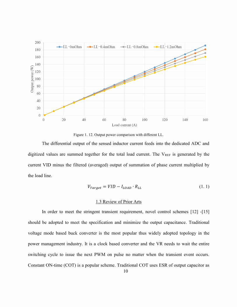
Figure 1. 12. Output power comparison with different LL. .............................................. 10
Figure 1. 13. Constant ON time. ....................................................................................... 11
Figure 1. 14. Simplified voltage mode COT architecture with ripple injection. .............. 12
Figure 1. 15. Simplified R4™ modules for PWM generation. ......................................... 13
Figure 1. 16. Simplified operation waveform during load transient. ................................ 14
Figure 1. 17. Schematic diagram of EAPP circuitry. ........................................................ 15
Figure 1. 18. Dual-Edge and Variable-Frequency Operational Waveforms. ................... 16

xii
Figure 2. 1. The architecture of the bidirectional multiphase synchronous controller. .... 19
Figure 2. 2. Small signal model of voltage mode buck converter. ................................... 21
Figure 2. 3. Generic type III compensation network. ....................................................... 22
Figure 2. 4. Digital control loop block diagram ................................................................ 23
Figure 2. 5. Root Locus..................................................................................................... 24
Figure 2. 6. Bode plot. ...................................................................................................... 24
Figure 2. 7. A power design breakdown in server application. ........................................ 25
Figure 2. 8. Power loss distribution of a synchronous buck in buck mode. ..................... 26
Figure 2. 9. Diode reverse-recovery waveforms ............................................................... 28
Figure 2. 10. Power loss distribution of a synchronous buck in boost mode. .................. 29
Figure 2. 11. Driver IC block diagram with proposed dead-time management. .............. 31
Figure 2. 12. Timing diagram of driver interface: (a) DR_EN is asserted; (b) DR_EN is
toggling during operation. ................................................................................................. 33
Figure 2. 13. Timing diagram of driver interface: PWM vs. Boot switch. ....................... 33
Figure 2. 14. LS turning ON/OFF. .................................................................................... 35
Figure 2. 15. Simulation result of LS turning ON/OFF. ................................................... 35
Figure 2. 16. An example of resonant gate-drive circuit. ................................................. 36
Figure 2. 17. Transfer ratio M vs. duty cycle D. ............................................................... 37
Figure 2. 18. Operational waveforms of PFM operation. ................................................. 38
Figure 2. 19. Power loss distribution of a synchronous buck in PFM. ............................. 39
Figure 2. 20. PFM to CCM transition (load: 1 A). ........................................................... 40

xiii
Figure 2. 21. LS VDS rising waveform due to diode reverse recovery. ............................ 41
Figure 2. 22. Discrete solution of the converter considering circuitry parasitics in the
buck mode. ........................................................................................................................ 42
Figure 2. 23. Simetrix simulation of Gate waveforms. ..................................................... 42
Figure 2. 24. HS VDS waveforms comparison. ................................................................. 43
Figure 2. 25. Light load CCM vs. PFM. ........................................................................... 44
Figure 2. 26. Power loss reduction (PFM minus CCM) vs. VID...................................... 45
Figure 2. 27. Efficiency vs. switching frequency. ............................................................ 46
Figure 2. 28. Efficiency vs. FET drive voltage. ................................................................ 47
Figure 2. 29. Measured efficiency of multiphase buck converter with operating different
number of phases. ............................................................................................................. 48
Figure 2. 30. Power efficiency optimization flow chart. .................................................. 49
Figure 2. 31. Diagram of Load adaptive control. .............................................................. 50
Figure 3. 1. DCR sense network RC time constant. ......................................................... 52
Figure 3. 2. The ATR timing architecture of the multiphase controller. .......................... 54
Figure 3. 3. Load engage response with pure voltage mode control. ............................... 55
Figure 3. 4. Load engage response w/ auto-phasing. ........................................................ 56
Figure 3. 5. Inductor current profile and gate-drive signals for the corresponding
operations. ......................................................................................................................... 57
Figure 3. 6. Load release response comparison. ............................................................... 58

xiv
Figure 3. 7. Inductor current slew rate difference during load release ............................. 59
Figure 3. 8. Adaptive body-braking control (pulsing control). ......................................... 60
Figure 3. 9. Flow chart of adaptive body-braking control (pulse control). ....................... 61
Figure 3. 10. Adaptive body-braking control (Body diode ON)....................................... 62
Figure 3. 11. Flow chart of adaptive body-braking control (Body diode ON). ................ 63
Figure 3. 12. Overshoot during phase shedding. .............................................................. 64
Figure 3. 13. Current balance block diagram. ................................................................... 65
Figure 3. 14. Simulated inductor current with smooth gain. ............................................ 66
Figure 3. 15. Simulation results of VR entering tri-state. ................................................. 67
Figure 3. 16. Simulation waveforms of existing long tri-state: (a) fixed dead-time: around
13 ns of shoot-through (b) adaptive dead-time: No shoot-through captured. ................... 68
Figure 3. 17. Operational waveforms of existing long tri-state: (a) around 10 ns of shoot-
through; (b) No shoot-through captured by PWM going low first when exiting tri-state. (c)
No shoot-through captured with “adaptive” shoot-though protection. ............................. 71
Figure 3. 18. Dead-time management diagram when VR exist tri-state ........................... 73
Figure 4. 1. PWM modulator diagram and VCOMP perturbation waveform: (a) PWM
Modulator; (b) modulation waveform with VCOMP perturbations. .................................... 75
Figure 4. 2. Frequency response of zero-order hold: (a) Gain; (b) Phase. ........................ 76
Figure 4. 3. Small-signal control block diagram of the closed loop output impedance. .. 77
Figure 4. 4. Plots of |Zv| and |ZOC| ..................................................................................... 79

xv
Figure 4. 5. Block diagram of load frequency detection (LFD). ...................................... 80
Figure 4. 6. A load transient response. Load step: 10A-141A, slew rate: 450 A/µS. Rep
rate: 400 kHz. (a) Nonlinear loop enabled. (b) Nonlinear loop disabled. ......................... 82
Figure 4. 7. Magnitude of an N-point DFT on VOUT (high frequency rep rate transient). (a)
Nonlinear loop enabled. (b) Nonlinear loop disabled. ...................................................... 83
Figure 4. 8. Phase currents oscillation: transient step: 132A-165A, load frequency 385
kHz. (a) LFD disabled. (b) LFD enabled. ......................................................................... 84
Figure 5. 1. The impact of DVS operation at datacenter level. ........................................ 86
Figure 5. 2. Operational waveforms with the critical dead times: (a) Buck (Source) CCM;
(b) Buck (Source) PFM; (c) Boost (Sink) Mode. ............................................................. 87
Figure 5. 3. Operational waveforms during mode transition. ........................................... 88
Figure 5. 4. System dynamic comparison of different driver twatch-dog. ............................. 89
Figure 5. 5. Experimental waveforms with different design of twatch-dog: (a) Boost (Sink)
mode: twatch-dog = 60 ns; (b) Boost (Sink) mode: twatch-dog = 120 ns. ................................ 90
Figure 5. 6. (a) Discrete solution of the converter considering circuitry parasitics in the
boost mode; (b) HS MOSFET enters avalanche due to high di/dt and parasitic inductance.
........................................................................................................................................... 92
Figure 5. 7. Equavelent circuitry with snubber when MOSFET is in off state. ................ 93
Figure 5. 8. Simulation result of HS VDS waveforms with different snuber resister Rfp. . 94

xvi
Figure 5. 9. High side VDS during repetitive DVID operation: (a) QRR = 20 nC and
without snubber circuitry; (b) QRR= 10 nC with snubber circuitry. Channel 2: HS drain-
source voltage, 5V/div. ..................................................................................................... 96
Figure 5. 10. The timing architecture of the multiphase controller. ................................. 97
Figure 5. 11. Architecture of DVID module with compensations. ................................... 98
Figure 5. 12. Matlab simulation result of DVID transition with and without droop
compensation and nonlinear control: (a) DVID upward transition; (b) DVID downward
transition. ........................................................................................................................ 100
Figure 5. 13. Experimental waveforms of fast DVID transitions with/without C·dV/dt
compensation: (a) Fast DVID upward transition; (b) Fast DVID downward transition. 102
Figure 5. 14. Simulation result of total phase current. (a) Source current at different VID
transition. (b) Sink current at different VID transition. .................................................. 104
Figure 5. 15. Negative current calculation in DVID downward transition. .................... 105
Figure 5. 16. Vout regulation comparison of different driver twatch-dog during DVID down.
......................................................................................................................................... 106
Figure 5. 17. A six phase synchronous buck converter with Intel VRTT. ..................... 108
Figure 5. 18. Input power consumption matrix(4×5×5): number of active phases in 5 VID
thresholds and repetative DVID operation. .................................................................... 109
Figure 5. 19. Phase number control based on VID delta. ............................................... 110

xvii
LIST OF TABLES
Table 2. 1 DIVER DEFINTION ....................................................................................... 34
Table 2. 2 THE CONVERTER PARAMETERS ............................................................. 49
Table 5. 1 Switching Characteristics .............................................................................. 107
Table 5. 2 MOSFET CHARACTERISTICS ................................................................. 107

xviii
LIST OF ACRONYMS
AVP Adaptive voltage positioning
PFM Pulse frequency modulation
CCM Continues conduction mode
DPWM Digital pulse width modulation
LL Load line
IIR Infinite impulse response
Qg MOSFET gate charge
RG MOSFET gate resistance
QRR Reverse recovery charge
FOM figure of merit
fSW Switching frequency
COSS Output capacitance
CDS Drain-source capacitance
CGD Gate-drain capacitance
CGS Gate-source capacitance
CDFP Drain-field plate capacitance
VSD Diode forward voltage drop
VGS(th) Gate-source threshold voltage
BVDSS Drain-Source Breakdown Voltage

xix
Rfp Snubber resister in MOSFET cell
VBUS Input voltage of the converter
VO Output voltage of the converter
VFET_DRV MOSFET driving voltage
DCR Direct current resistance
LSB Least significant bit
GPIB General purpose interface bus
ZCS Zero current switching
ZVS Zero voltage switching

1
CHAPTER ONE: INTRODUCTION
Power conversion techniques have been continuing to be the focus in the power
management industry. With ever increasing the emphasis on power efficiency, switch mode
power supplies and power management ICs are extensively used in automotive, smart phones,
TVs, desktop PCs, servers, notebooks and etc. According to IMS research [1] power
management & driver IC reaches $13.9567 billion in revenue in the fiscal year 2011.
The current and forecast worldwide market for power management ICs shipment (units in
million) are shown in Figure 1. 1. [1] .
Figure 1. 1. The world market for power management IC by application.

2
Figure 1. 2. Voltage regulator real estate in server motherboard.
This is the newly released Dell PowerEdge R620 Server motherboard. It can support two
150 W high end CPUs and 4 memory channels up to 768GB of memory (32GBx24dimms). The
multiphase voltage regulators, 2 for CPU, 4 for MEM and the rest point of load (POL) VRs are
highlighted in red. The VRs convert 12V DC from the PSU output to various voltage levels to
power up the CPUs, memories, hard drives, ASICs on board and peripheral cards. It occupies
more than 10% area of the motherboard.

3
Figure 1. 3. A typical power management map for server system.
Figure 1. 3 shows a simplified power management map for a typical 2S (socket) server
system. System interaction is eliminated in the illustration and the focus is only on the power
conversion.

4
1.1 Introduction to Multiphase Buck Converter
As the complexity and number of transistors exponentially rise in the modern high end
processors, the supply current specification is common to be above 100A. Paralleling the
regulators is the only way to alleviate the thermal stress on the power components (power
MOSFETs, power inductor). Therefore, multiphase buck converter has been employed in the
power conversion field. Although the initial concept has been adopted in power management
industry for quite a while, there are still a lot of areas worth investigating due to the increasing
complexity of the power architecture and growing focus on the green energy. Green energy here
refers to less power conversion loss and less output capacitors.
Figure 1. 4. A multiphase synchronous buck converter for CPU application.
Figure 1. 5 shows the relationship of normalized ripple current between duty cycle and
phase number.

5
Figure 1. 5. Normalized ripple current as a function of phase number and duty cycle.
The benefits of adopting multiphase buck converter in the design are bulleted as follows:
Decreased IRMS and reduced power loss;
Increased inductor current slew rate: 𝐿𝑒𝑓𝑓𝑒𝑐𝑡𝑖𝑣𝑒 =𝐿
𝑁𝑝ℎ𝑎𝑠𝑒;
Output inductor current cancellation and voltage ripple reduction;
Optimized efficiency over the whole load range, especially, in light load
o Load adaptive control(LAC)
o Pulse skipping control(PFM)
Better dynamic voltage regulation capability
However, with those advantages, there are challenges that the multiphase converter have
brought in as well. The challenges are the major focus of this dissertation.

6
Figure 1. 6. A typical power delivery path for today’s microprocessors.
Figure 1. 6 shows a typical power delivery path for today’s microprocessors. With all the
mechanical restriction, the power inductors and output capacitors need to be placed close to the
processors in order to reduce the power distribution loss.
Figure 1. 7 Power distribution impedance versus frequency.
Closed-loop output impedance of voltage regulator is an important specification in the
frequency domain. Figure 1. 7 [2] shows the output impedance plot of a power supply for CPU
application with AVP. The output impedance, as shown by the red curve, is determined by the

7
power supply's AVP design value within the loop bandwidth of the VR. At higher frequency, the
output impedance will be dominated by the ESL of MLCC and the socket.
Figure 1. 8 shows the pyramid of server power design. Robustness is of the top priority in
the power design since the system are running with various kinds of customer’s data, some of
which are very critical. The power related failures can stop the transaction or communication and
would create substantial loss. The power conversion efficiency is the foundation of the power
design. Design parametric optimization and latest silicon technology adoption should be
rigorously studied. Functionality, such as, phase shedding control and load transient
enhancements, shows the advancement of the design and can improve the system reliability,
efficiency and reduce the cost. Cost reduction is the final step to optimize the design and give
environment less burden.
Figure 1. 8. Robustness, efficiency and cost pyramid in server power design.
Reliability
Efficiency
Functionality
Cost

8
1.2 Adaptive Voltage Positioning
Due to the working mode of the processors, load transient is an important design
requirement for multiphase synchronous buck converter. Adaptive voltage positioning (AVP)
has been adopted to lower the power dissipation, especially at heavy load [3] - [5] . The
introduced constant output impedance reduces the value of output capacitance.
Figure 1. 9 illustrates the comparison results of AVP implementation when load transient
events occur. The introduced AVP window can be fully utilized to optimize the load transient.
Figure 1. 9. Load transient without and with AVP implementation.

9
Figure 1. 10. AVP design in analog realization.
Figure 1. 10 illustrates the block diagram of AVP design in an analog realization [6]
Figure 1. 11. AVP design in digital realization.
To make it simple, the adaptive voltage position (AVP) design is to use the entire AVP
window for voltage excursions during the transient event. As depicted in Figure 1. 12, another
design benefit of adopting AVP scheme is that the output power of the multiphase VR at full
load, thus, less thermal burden compared to the implementation without AVP.
10
Figure 1. 12. Output power comparison with different LL.
The differential output of the sensed inductor current feeds into the dedicated ADC and
digitized values are summed together for the total load current. The VREF is generated by the
current VID minus the filtered (averaged) output of summation of phase current multiplied by
the load line.
𝑉𝑇𝑎𝑟𝑔𝑒𝑡 = 𝑉𝐼𝐷 − 𝐼𝐿𝑂𝐴𝐷 ∙ 𝑅𝐿𝐿 (1. 1)
1.3 Review of Prior Arts
In order to meet the stringent transient requirement, novel control schemes [12] -[15]
should be adopted to meet the specification and minimize the output capacitance. Traditional
voltage mode based buck converter is the most popular thus widely adopted topology in the
power management industry. It is a clock based converter and the VR needs to wait the entire
switching cycle to issue the next PWM on pulse no matter when the transient event occurs.
Constant ON-time (COT) is a popular scheme. Traditional COT uses ESR of output capacitor as

11
output current feedforward term to initial the pulse. Current mode hysteretic control [17] [18] is a
very popular topology to achieve fast transient response. It uses sensed/synthetic inductor current
to compare against the hysteresis band. In [18] authors propose current mode hysteretic control
that can accomplish the AVP by the natural hysteresis band, however, the fairly constant
hysteretic window cannot pull in the pulse fast enough when the transient event occurs.
1.3.1 Constant ON-time (COT)
Constant ON-time (COT) is a popular frequency modulation scheme which is capable of
achieving fast transient response.
Figure 1. 13. Constant ON time.
The core of the modulator is the one-shot that sets the HS ON-time. The TON, as shown in
(1.2), is inversely proportional to VIN and proportional to the VOUT:
𝑇𝑂𝑁 = 𝑇𝑆𝑊𝑉𝑂𝑈𝑇
𝑉𝐼𝑁 (1. 2)
As shown in Figure 1. 13, when VFB becomes lower than VREF, the next ON period is
initiated. On pulse period stays for a predetermined period as equation (1.2) indicates. The clock-
less architecture shows the advantage that the HS pulse can be initiated sooner when transient

12
event occurs. There will be a minimum OFF-time between the HS pulses to guarantee the current
sensing purpose. The minimum OFF-time also decides the maximum duty cycle that the VR can
support.
Figure 1. 14. Simplified voltage mode COT architecture with ripple injection.
The D-CAP2 control scheme [19] , introduced by Texas instruments, includes an internal
ripple generation circuitry, RCC, as the red block in Figure 1. 14. Compared with first generation
of D-CAP, multi-layer ceramic capacitors (MLCC) solution with very low ESR can be used due
to the ripple injection. The hybrid control mode is to employ the emulated inductor current ripple
and then combine it with the voltage feedback signal.
To meet small-signal stability, the output capacitance value should be governed by (1.3)
5 × 𝑓𝐶2 ≤=R𝐶1×C𝐶1×0.6×(0.67+𝐷)
2π×G×L×𝐶𝑂𝑈𝑇×𝑉𝑂𝑈𝑇≤
𝑓𝑆𝑊
3 (1. 3)
where G =0.25. RC1× CC1 time constant can be referred to TPS53819 datasheet. D is the duty
cycle.

13
1.3.2 Current Mode Hysteresis
Hysteretic control is a very popular topology for fast transient required application. A
drawback of traditional hysteretic control from the static point of view is the switching frequency
is variable (clock-less), which is defined by parasitic elements, primarily the ESR of the output
capacitor. Advanced hysteretic control incorporates the frequency control (phase-locked loop) to
stabilize the switching frequency.
Intersil refers to the R4 (Robust Ripple Regulator as described with R3) Modulator as a
“Current-Mode Hysteretic” modulator (CMH). It is a variable frequency switching architecture
which operates without a clock and uses a hysteretic band against which a “current” signal is
compared. However, true inductor current is not used for the modulation, unlike a true current-
mode controller. A synthesized (synthetic) current ripple is generated and compared against the
hysteretic window that is created relative to the voltage loop feedback to determine power switch
on and off times. Also there is no compensating ramp utilized. The architecture does not make
use of any voltage feedback compensation and no integrator. Therefore it has the capacity for
fast transient response and easier deployment of a design.
Figure 1. 15. Simplified R4™ modules for PWM generation.

14
Figure 1. 15 [22] shows the modulator core of the R4 controller, the error-amplifier,
synthetic current generator and the hysteretic window comparator. The error voltage, generated
by the VDAC minus feedback, compares against monitors the synthetic current signal against
and corresponding window voltage to determine the PWM switching events.
Figure 1. 16. Simplified operation waveform during load transient.
Figure 1. 16 [22] shows the operational waveform during load assertion and load release.
Switching frequency, as the magenta curve indicates, speeds up during load assertion and slows
down during load release. Both PWM edges are modulated since the synthetic current compares
against Hysteric upper window and VCOMP voltage.

15
1.3.3 EAPP
Minimizing the delay in control loop is critical during transient event. Based on the
advantages of trailing/leading edge modulation during turning OFF/ON, the enhanced active
pulse positioning (EAPP) is able to minimize both ON/OFF delays by combining the schemes as
discussed in [24] .
Figure 1. 17. Schematic diagram of EAPP circuitry.
The simplified block diagram and the corresponding operational waveforms are
illustrated in Figure 1. 17. During transient event, EAPP will turn on PWM early (from t3 to t2)
and move the next PWM ahead (from t8 to t7) to reduce the blanking time. Figure 5 shows
transient load engage response of 3-phase VR with EAPP [24] , [25] .

16
Figure 1. 18. Dual-Edge and Variable-Frequency Operational Waveforms.
1.4 Dissertation Outlines
The primary focus and objective of the dissertation is to comprehensively investigate the
current and voltage dynamics of the multiphase synchronous buck converter. We focus on
optimizing the topology to achieve best efficiency and highest possible reliability based on the
real system running condition and corner case scenarios.
In chapter 1, we introduce the background information of the importance of power
management IC in different business sectors, then the scenario multiphase synchronous buck
converter and briefly talk about the AVP design that can reduce output capacitors and power
dissipation. The ongoing research and advanced control topologies are reviewed and several
nonlinear control schemes are studied
In chapter 2, we start the efficiency optimization from static operation. First, we design
the compensation of the voltage mode controller with digitized format. We meticulously study

17
the power loss in several modes of operation, i.e. buck, PFM and boost modes, which cover all
the operation scenarios of CPU VR. Driver interface is thoroughly investigated here for
operation and efficiency purposes. Switching waveforms are understood better with all the
parasitics. An efficiency optimization routine is generated by parametric variation.
In chapter 3, we propose the load transient enhancement schemes to minimize the output
voltage excursion during low repetitive load transient. We first study the DCR current sense
impact for the AVP loop, which can effectively shape the output voltage excursion. During load
engage, the pulse should be pulled in fast enough to compensate the voltage deviation. During
load release, adaptive body braking schemes are proposed to adaptively suppress the voltage
overshoot during load release. Special design consideration needs to be carried out during slow
phase shedding that the inductor current in the shedded phase needs to be ramped down to zero
before turn OFF the phase. A corner case operation with potential power MOSFETs shoot-
through is captured and new dead-time management scheme is proposed to maintain the high
efficiency, eliminate the shoot-through and hence ensure the system reliability.
In chapter 4, we first study the sampling nature of PWM converter. The closed loop
system output impedance is derived and the compensation network are optimized in the high
frequency range to attenuate the high frequency system noise. Beat frequency is studied and load
frequency detection scheme and current protection in the control loop are proposed to mitigate
the issue and bound the phase current.
Multiphase converter design capable of dynamic voltage scaling (DVS) is presented in
chapter 5. Modes of operation are thoroughly studied first. Optimized driver dead-time in boost

18
mode operation are illustrated and DVID downward transition can be achieved with shared phase
current. The excessive stress on the control MOSFET which increases the reliability concern is
captured in boost mode operation. Feasible solutions are also proposed and verified by both
simulation and experiment results. CdV/dt compensation for removing the AVP effect and novel
nonlinear control scheme for smooth transition are proposed for dealing with fast voltage
positioning. Optimum phase number control during dynamic voltage transition is also proposed
and triggered by voltage identification (VID) delta to further reduce the dynamic loss.
Chapter 6 presents the conclusions and the future work is outlined.

19
CHAPTER TWO: OPTIMIZATION ON STATIC OPERATION
Figure 2. 1. The architecture of the bidirectional multiphase synchronous controller.

20
Figure 2. 1 shows the architecture of the multiphase synchronous buck converter which
can be working in the bidirectional fashion. Each phase is interleaved by 360/NPHASE to achieve
optimal ripple cancellation. In the controller section, the main sub-circuit modules are illustrated.
Current ADC module samples and digitizes each phase current, which is the voltage across the
cap of inductor DCR the sense network, in the real time manner. Voltage ADCs sense and
digitize both the VOUT and VBUS, and the digitized VBUS acts as feed-forward term in the control
loop. Adaptive voltage positioning (AVP) module decodes the VID command and generates the
reference based the digitized total phase current information with DVID compensation. Digital
compensator filters the error voltage generated by ADC output and AVP blocks and feeds into
the DPWM generator block. Current balance module, which is designed as 1/5 of the voltage
loop, and Nonlinear PWM generator both modifies DPWM patterns in different fashions. The
control outputs of DPWM generators are the PWM and driver enable (DR_EN) signals.
2.1 Compensation Design
Compensator design is the core of VR design [7] [8] . As shown in Figure 2. 2, a small
signal ac model is presented. Vout(s) is the function of the reference voltage Vtarget(s), line input
voltage Vin(s) and the output load current Iout(s). The design objective is the VR capable of
rejecting the disturbances of the line input voltage and output load current, good transient
response and stability.

21
Figure 2. 2. Small signal model of voltage mode buck converter.
𝑣𝑜𝑢𝑡(𝑠) = 𝐺𝑣𝑑(𝑠)��(𝑠) + 𝐺𝑣𝑔(𝑠)��𝑖𝑛(𝑠) − 𝑍𝑜(𝑠)𝑖𝑜𝑢𝑡(𝑠) (2. 1)
𝐺𝑣𝑑(𝑠) =��𝑜𝑢𝑡(𝑠)
��(𝑠)|��𝑜𝑢𝑡(𝑠)=0��𝑖𝑛(𝑠)=0 =
𝑉𝑖𝑛(1+𝑠𝑅𝐸𝑆𝑅𝐶𝑂𝑈𝑇)𝑅𝐿𝑜𝑎𝑑
(𝑅𝐿𝑜𝑎𝑑+𝑅𝐷𝐶𝑅)
𝑠2𝐿𝐶𝑂𝑈𝑇(𝑅𝐿𝑜𝑎𝑑+𝑅𝐸𝑆𝑅𝑅𝐿𝑜𝑎𝑑+𝑅𝐷𝐶𝑅
)+𝑠(𝐿
𝑅𝐿𝑜𝑎𝑑+𝑅𝐷𝐶𝑅+𝐶𝑂𝑈𝑇𝑅𝐸𝑆𝑅+𝑅𝐿𝑜𝑎𝑑//𝑅𝐷𝐶𝑅)+1
(2. 2)
𝑍𝑜(𝑠) =��𝑜𝑢𝑡(𝑠)
��𝑜𝑢𝑡(𝑠)|��𝑜𝑢𝑡(𝑠)=0��(𝑠)=0 =
(1+𝑠𝐿
𝑅𝐷𝐶𝑅)(1+𝑠𝑅𝐸𝑆𝑅𝐶𝑂𝑈𝑇)
𝑅𝐿𝑜𝑎𝑑𝑅𝐷𝐶𝑅(𝑅𝐿𝑜𝑎𝑑+𝑅𝐷𝐶𝑅)
𝑠2𝐿𝐶𝑂𝑈𝑇(𝑅𝐿𝑜𝑎𝑑+𝑅𝐸𝑆𝑅𝑅𝐿𝑜𝑎𝑑+𝑅𝐷𝐶𝑅
)+𝑠(𝐿+𝑅𝐿𝑜𝑎𝑑𝑅𝐷𝐶𝑅+𝐶𝑂𝑈𝑇𝑅𝐸𝑆𝑅(𝑅𝐿𝑜𝑎𝑑+𝑅𝐷𝐶𝑅)
𝑅𝐿𝑜𝑎𝑑+𝑅𝐷𝐶𝑅)+1
(2. 3)
𝐺𝑣𝑔(𝑠) =��𝑜𝑢𝑡(𝑠)
��𝑖𝑛(𝑠)|��𝑜𝑢𝑡(𝑠)=0��(𝑠)=0 = 𝐷
𝑅𝐷𝐶𝑅(1+𝑠𝑅𝐸𝑆𝑅𝐶𝑂𝑈𝑇)
𝑅𝐿𝑜𝑎𝑑+𝑅𝐷𝐶𝑅
𝑠2𝐿𝐶𝑂𝑈𝑇(𝑅𝐿𝑜𝑎𝑑+𝑅𝐸𝑆𝑅)
𝑅𝐿𝑜𝑎𝑑+𝑅𝐷𝐶𝑅+𝑠
(𝐿+𝐶𝑂𝑈𝑇(𝑅𝐸𝑆𝑅(𝑅𝐿𝑜𝑎𝑑+𝑅𝐷𝐶𝑅)+𝑅𝐿𝑜𝑎𝑑𝑅𝐷𝐶𝑅)
𝑅𝐿𝑜𝑎𝑑+𝑅𝐷𝐶𝑅+1 (2. 4)
𝑇𝑣(𝑠) = 𝐺𝐶(𝑠)𝐹𝑀𝐺𝑣𝑑(𝑠) (2. 5)
The derivation is based on the state-space averaging model.
Gvd(s) is a state-space averaging model for the plant, which represents open loop control-
to-output voltage transfer function.
Zo(s) is the output current-to-output voltage transfer function.
Gvg(s) is the open loop input-to-output voltage transfer function.

22
2.1.1 Direct Digital Design
Due to the double pole of output filter in the voltage mode control, as shown in Figure 2.
3, two zeros from the type III compensation network are needed so that the phase can be boosted
by 180 degrees. There are two methods to design the digital compensation network:
(1) Emulation method, design the analog compensation first in Laplace domain and
transfer to digital domain.
(2) Direct digital design, design the compensation network in digital domain by first
digitizing the plant.
Figure 2. 3. Generic type III compensation network.

23
Figure 2. 4. Digital control loop block diagram
To digitize the plant, there are several methods can be used, for example Zero-Pole
matching (ZPM), Impulse Invariant Mapping, as well as, Tustin approximation. We use ZPM as
the method of conversion. The matched DC gains is necessary for analog and discretized systems.
The zeros and poles are transformed by the following equation:
𝑧𝑖 = 𝑒𝑠𝑖/𝐹𝑆 (2. 6)
where, si is the ith pole or zero of the continuous-time system. zi is the ith zero or pole of the
discretized system accordingly. FS is the sampling frequency.
2.1.2 Root Locus and Bode Plot
Root locus is a graphical technique of studying the roots (poles and zeros) of the
characteristic equation of a linear system [9] . Matlab SISO design tool [10] can be utilized to
move the poles and zeros location so that the desired system bandwidth and phase margin can be
guaranteed.

24
Figure 2. 5. Root Locus.
Figure 2. 5 shows the system root locus plot using Matlab.
Figure 2. 6. Bode plot.
Figure 2. 6 shows the compensator gain in frequency domain. KI and KD are dominating
in both low frequency and high frequency ranges. KP maintains compensator gain in middle
frequency range, which affects loop BW. Kfp is essential for high frequency noise reduction
which rolls off loop gain at high frequency.

25
2.2 Power Loss Analysis
In order to support various system running configuration, the VR design (multiphase +
single phase) in server application need to cover the entire loading condition and then budget
wisely. Figure 2. 7 shows a typical power budget in percentage scale.
Figure 2. 7. A power design breakdown in server application.
The power conversion loss [26] - [29] should be understood well first then optimized
accordingly. Due to the different operation modes of buck converter, the loss model is divided in
three cases, CCM buck, CCM boost and PFM buck, respectively. The corresponding power loss
representations with inductor current profiles are shown in Figure 2. 8, Figure 2. 10 and Figure 2.
19, respectively.

26
Figure 2. 8. Power loss distribution of a synchronous buck in buck mode.
Power loss simulation and experimental verification should be both carried out with
varying switching frequency and PVCC( MOSFET drive voltage). The following equations
shows power loss portion when the VR is operating in synchronous buck mode.
The recent development of power MOSFETs has been focusing on the ultra-low channel
resistance and ultra-fast switching speed. FOM is a fast measure to gauge the MOSFET under
the same breakdown voltage. Infineon’s OptiMOSTM and Fairchild Semi’s PowerTrench® are
considered industry leading technologies of low voltage power MOSFETs.
FOM = 𝑅𝑑𝑠_𝑂𝑁 ∙ 𝑄𝑔 (2. 7)
The conduction loss is the resistive loss due to current conducted through the channel
resistance Rds_ON.
𝑃𝐶𝑂𝑁𝐷 = 𝐼𝑅𝑀𝑆2 ∙ 𝑅𝑑𝑠_𝑂𝑁 (2. 8)

27
𝐼𝑅𝑀𝑆(𝐿𝑆) = √(𝐼𝑜𝑢𝑡2
𝑁2−𝐼𝑟𝑖𝑝𝑝𝑙𝑒2
12) (1 − 𝐷) (2. 9)
𝐼𝑅𝑀𝑆(𝐻𝑆) = √(𝐼𝑜𝑢𝑡2
𝑁2+𝐼𝑟𝑖𝑝𝑝𝑙𝑒2
12)𝐷 (2. 10)
PCOSS is the power loss caused by the output capacitance of MOSFET
𝑃𝐶𝑂𝑆𝑆 = 0.5 ∙ 𝑄𝑂𝑆𝑆 ∙ 𝑉𝐵𝑈𝑆 ∙ 𝑓𝑆𝑊 (2. 11)
Pdeadtime represents the body diode conduction loss during tdeadtime.
𝑃𝑑𝑒𝑎𝑑𝑡𝑖𝑚𝑒 = 𝑉𝑆𝐷 ∙ 𝑓𝑆𝑊 ∙ [(𝐼𝑂𝑈𝑇 −𝐼𝑟𝑖𝑝𝑝𝑙𝑒
2) 𝑡𝑑𝑒𝑎𝑑𝑡𝑖𝑚𝑒(𝑟) + (𝐼𝑂𝑈𝑇 +
𝐼𝑟𝑖𝑝𝑝𝑙𝑒
2) 𝑡𝑑𝑒𝑎𝑑𝑡𝑖𝑚𝑒(𝑓)] (2. 12)
where VSD is diode forward voltage drop; tdeadtime(r) represents rising edge dead-time
between LS turn off and HS turn on; tdeadtime(f) represents rising edge dead-time between HS turn
off and LS turn on.
PQRR, the LS body diode reverse-recovery loss, is induced during the phase of turning off
of the LS body diode.
𝑃𝑄𝑅𝑅 = 𝑄𝑅𝑅(𝐿𝑆) ∙ 𝑉𝐵𝑈𝑆 ∙ 𝑓𝑆𝑊 (2. 13)
where QRR is the excess minority carrier charge in the reverse recovery transient.

28
Figure 2. 9. Diode reverse-recovery waveforms
In the buck mode operation, the LS MOSFET is considered as soft switching. The HS
MOSFET turn on/off loss incorporating common source inductance due to device package can
be accurately calculated by:
𝑃𝑆𝑊(𝑂𝑁) = 𝑉𝐵𝑈𝑆 ∙ 𝑓𝑆𝑊 ∙ (𝐼𝑂𝑈𝑇 −𝐼𝑟𝑖𝑝𝑝𝑙𝑒
2) ∙
(
0.5∙𝑄𝑔𝑠2(𝐻𝑆)
𝑉𝐹𝐸𝑇𝐷𝑅−𝑉𝑃𝐿(𝐻𝑆)
𝑅𝑔(𝐻𝑆)+𝑅𝑑𝑟𝑖𝑣𝑒𝑟+𝐿𝑐𝑠𝑖∙𝐼𝑂𝑈𝑇−
𝐼𝑟𝑖𝑝𝑝𝑙𝑒2
𝑄𝑔𝑠2(𝐻𝑆)
+
0.5∙𝑄𝑔𝑑(𝐻𝑆)
−(𝑅𝑔(𝐻𝑆)+𝑅𝑑𝑟𝑖𝑣𝑒𝑟)+√(𝑅𝑔(𝐻𝑆)+𝑅𝑑𝑟𝑖𝑣𝑒𝑟)2+4𝐿𝑐𝑠𝑖∙𝑄𝑂𝑆𝑆(𝐿𝑆)
𝑄𝑔𝑑(𝐻𝑆)2 (𝑉𝐹𝐸𝑇𝐷𝑅
−𝑉𝑃𝐿(𝐻𝑆))
2𝐿𝑐𝑠𝑖∙𝑄𝑂𝑆𝑆(𝐿𝑆)
𝑄𝑔𝑑(𝐻𝑆)2 )
(2. 14)

29
𝑃𝑆𝑊(𝑂𝑁) = 𝑉𝐵𝑈𝑆 ∙ 𝑓𝑆𝑊 ∙ (𝐼𝑂𝑈𝑇 +𝐼𝑟𝑖𝑝𝑝𝑙𝑒
2) ∙
(
0.5∙𝑄𝑔𝑠2(𝐻𝑆)
𝑉𝑃𝐿(𝐻𝑆)
𝑅𝑔(𝐻𝑆)+𝑅𝑑𝑟𝑖𝑣𝑒𝑟+𝐿𝑐𝑠𝑖∙𝐼𝑂𝑈𝑇+
𝐼𝑟𝑖𝑝𝑝𝑙𝑒2
𝑄𝑔𝑠2(𝐻𝑆)
+
0.5∙𝑄𝑔𝑑(𝐻𝑆)
−(𝑅𝑔(𝐻𝑆)+𝑅𝑑𝑟𝑖𝑣𝑒𝑟)+√(𝑅𝑔(𝐻𝑆)+𝑅𝑑𝑟𝑖𝑣𝑒𝑟)2+4𝐿𝑐𝑠𝑖∙𝑄𝑂𝑆𝑆(𝐿𝑆)
𝑄𝑔𝑑(𝐻𝑆)2 (𝑉𝑃𝐿(𝐻𝑆))
2𝐿𝑐𝑠𝑖∙𝑄𝑂𝑆𝑆(𝐿𝑆)
𝑄𝑔𝑑(𝐻𝑆)2 )
(2. 15)
where IOUT, VBUS, VFET_DR, Rg, VPL, Rdriver, Lcis, Qds and Qgd are the output current, Bus
voltage, gate drive voltage, gate drive resistance, HS MOSFET plateau voltage, HS MOSFET
source inductance, current, HS MOSFET Qds and HS MOSFET Qgd, respectively.
The gate charge induced loss:
𝑃𝑔𝑎𝑡𝑒 = (𝑄𝑔(𝐻𝑆) + 𝑄𝑔(𝐿𝑆)) ∙ 𝑉𝐹𝐸𝑇_𝐷𝑅 ∙ 𝑓𝑆𝑊 (2. 16)
The switching frequency and VFET_DR should be optimally selected based on the minimum
power loss.
Figure 2. 10. Power loss distribution of a synchronous buck in boost mode.

30
When the inductor current flow reversely, as shown in Figure 2. 10, the converter is
enforced working in sink mode, or boost mode. The loss formulas change accordingly. HS power
MOSFETs are soft switching.
𝑃𝑄𝑅𝑅 = 𝑄𝑅𝑅(𝐻𝑆) ∙ 𝑉𝐵𝑈𝑆 ∙ 𝑓𝑆𝑊 (2. 17)
LS power MOSFETs are consequently hard switching in the boost mode. The simplified
turn ON/OFF losses are:
𝑃𝑆𝑊(𝑂𝑁) = (𝑉𝐵𝑈𝑆 + 𝑉𝑆𝐷) ∙ 𝑓𝑆𝑊 ∙ (𝐼𝑂𝑈𝑇 +𝐼𝑟𝑖𝑝𝑝𝑙𝑒
2) ∙ (
𝑄𝑆𝑊𝑉𝐹𝐸𝑇_𝐷𝑅−𝑉𝑃𝐿𝑅𝑔+𝑅𝑑𝑟𝑖𝑣𝑒𝑟
) (2. 18)
𝑃𝑆𝑊(𝑂𝐹𝐹) = (𝑉𝐵𝑈𝑆 + 𝑉𝑆𝐷) ∙ 𝑓𝑆𝑊 ∙ (𝐼𝑂𝑈𝑇 −𝐼𝑟𝑖𝑝𝑝𝑙𝑒
2) ∙ (
𝑄𝑆𝑊𝑉𝐹𝐸𝑇_𝐷𝑅−𝑉𝑃𝐿𝑅𝑔+𝑅𝑑𝑟𝑖𝑣𝑒𝑟
) (2. 19)
2.3 Driver Interface
One phase of the multiphase synchronous buck converter with the dead-times
management is shown in Figure 2. 11. Dead time tdead − time [30] during which both power
MOSFETs (Q1 and Q2) are off, is inserted between the gate signal cycle to avoid cross-
conduction and guarantee safe operation of the circuitry. There is another dead time which is
very critical in the driver IC design for the DVID downward operation, i.e. watch-dog timer
twatch-dog, which is defined as from HS gate signal is low and switch node is still high, after this
defined time length, the LS MOSFET is turning on. The detailed analysis of system impact by
twatch-dog is in chapter V.

31
Figure 2. 11. Driver IC block diagram with proposed dead-time management.
Dead-time must be sufficient enough to guarantee no cross conduction between high &
low side MOSFETs. However, a longer dead-time will bring in more switching power loss to a
VR since the body diode but not channel of low-side MOSFET turn on during dead-time. On the
other hand, a shorter dead-time may increase risk of cross-conduction. Therefore, Dead-time
management is critical in a MOSFET driver, which will directly impact VR efficiency and
reliability.
The discrete driver dead-time design should consider MOSFET parameter variation (RG,
CISS, VGS(TH)) and the dead-time should be adaptive to the MOSFETs. The adaptive dead-time
scheme measures the actual voltage on the gate and only when the voltage on the gate is below a
proper value (1V, since this is a good value for 90% of the MOSFET), the transition is allowed
to turn on the other gate. Adaptive dead-time control has been used in a general MOSFET driver

32
circuitry that can drive discrete MOSFETs. Adaptive dead time is the improvement of the long
fixed dead-time (fixed delay block). As a result, actual dead-time is usually pretty long (12ns is
the best from industrial leading suppliers).Dead-time impacts the system efficiency as discussed
in (2.12). To reduce the dead-time and QRR loss, LS Schottky barrier diode (VSD = 0.56V,
Infineon BSC014NE2LSI) should be incorporated in the design. By calculation, adding extra 5
ns dead-times will result in 0.2% of efficiency penalty.
Integrated power stage containing MOSFETs and driver has been increasingly used in
recent years especially for high density design such as blade server. In order to boost the power
conversion efficiency, the fixed driver dead-time with simpler logics can be used in a power
stage since parasitic MOSFET parameters inside power stage package is predictable and in a
relatively small variation range. However, the fixed driver dead-time may create a shoot-through
scenario in a multiphase VR when the shedded phases are in tri-state for a long period, then
recovered to operation mode. Both MOSFETS are kept in the OFF state when the driver receives
a PWM tri-state signal.
PWM and DR_EN are both control input signals for driver IC which are generated by the
state machine of PWM controller. Figure 2. 12 shows the timing diagram of driver interface with
HiZ management. HiZ here refers to the high-impedance stage by keeping all MOSFETs in off
state. HiZ window is defined as voltage range of the PWM between 1.2 V and 2.2 V for a 3.3 V
application. t1 and t3 represent propagation delay of LS Gate and HS Gate, respectively. t2 and t4
represent dead times from LS falling and HS falling, respectively. t5 and t8 both represent hold-off
times. t6 and t7 represent propagation delay of DR_EN rising and falling.

33
(a) (b)
Figure 2. 12. Timing diagram of driver interface: (a) DR_EN is asserted; (b) DR_EN is toggling during
operation.
Figure 2. 13 shows timing diagram of the boot switch which is embedded inside of driver.
The boot switch is ON when the LS is ON to charge the bootstrap capacitor. The boot switch is
OFF when the HS is ON. During PWM HiZ, the switch must remain OFF since the negative
current can discharge the boot cap if the switch is ON.
Figure 2. 13. Timing diagram of driver interface: PWM vs. Boot switch.

34
To obtain the optimum static efficiency for the whole load range, not only the lower
FOM of power MOSFETs should be employed, the driver capability and the parameters
associated with the power loss should be carefully studied and optimally defined. Finally, phase
shedding control needs to be implemented to improve the efficiency in mid-light load, and the
control thresholds are the intersection points of adjacent phases in efficiency plot.
Table 2. 1 DIVER DEFINTION
Upper driver source/sink current 2A / 2A
Upper driver source/sink impedance
Lower driver source/sink current
Lower driver source/sink impedance
tdeadtime(f)
0.8 Ohm / 0.6 Ohm
2A / 4A
0.8 Ohm / 0.35 Ohm
8 ns
tdeadtime(r) 15 ns
It’s very important to correctly define and strengthen the driving capability of the power
MOSFETs driver to minimize the HS switching loss during commutation (the overlapped area).
TABLE I shows the definition of driving capability and dead times. The low sink impedance is
extremely important to avoid Cdv/dt induced turn on phenomenon (shoot-through) [32] in the LS
MOSFET during the fast turn on of HS MOSFET.

35
Figure 2. 14. LS turning ON/OFF.
Figure 2. 14 shows color coded procedures of LS MOSFET turning ON/OFF. The speed
of turning ON and OFF is limited by the parasitic RLC as illustrated in the loop. The red arrows
in Figure 2. 15 represents the peak source and sink current, respectively. Sink current needs to be
bigger to avoid the shoot-through. There is also a need of minimum OFF time latch in the driver
design to ensure the energy on the gate are fully discharged when turn OFF.
Figure 2. 15. Simulation result of LS turning ON/OFF.

36
Figure 2. 16. An example of resonant gate-drive circuit.
Figure 2. 16 [33] shows a resonant gate driver structure. It is an interesting idea that the
energy on the gate can be recovered by the resonance [33] - [35] . However, it is not applicable
for the hard switching design. The loss analysis from the previous section reveals that the gate
drive loss is only the smallest portion in a typical design. Moreover, a resonant gate driver puts
timing constraints on the switching transitions (MOSFETs are not driven hard) and the switching
goes from inductively limited to MOSFET limited. That means that the dynamic losses will
increase substantially. The only way to resolve this is to have an entirely resonant buck topology.
With the larger phase currents, this offsets the benefits by additional conduction loss.
2.4 Light Load Operation
Reducing power conversion loss during light load is one of the major focus in computing
industry [36] [37] The power saving features should be implemented in VR. In this dissertation,

37
we treat the terms, diode emulation (DE), discontinuous conduction mode (DCM), pulse
skipping, and pulse frequency modulation (PFM) the same.
The voltage gain during PFM can be found:
𝑀 =2
1+√1+8𝐼𝑂𝑈𝑇𝐿
𝑇𝑂𝑁2 𝑓𝑆𝑊
(2. 20)
where 𝑀 =𝑉𝑜𝑉𝑖𝑛⁄ , TON is the ON time of the control MOSFET. L is the per phase
inductance. IOUT is the load current.
Figure 2. 17. Transfer ratio M vs. duty cycle D.
Assume TON is constant during PFM, the fSW is linearly proportional to the load current to
achieve the same regulation of the output voltage. Therefore, the light load efficiency can be
improved since the switching frequency can be decreased based on the load condition.

38
From Figure 2. 12, we can easily find
𝜏 = 𝐼𝑂𝑈𝑇𝐿𝑓𝑆𝑊 (2. 21)
τ is the normalized inductor time constant.
When CPU is in idle state, it is normally the condition of load current less than half of the
inductor current ripple. The VR should be operating in PFM to reduce power loss [36] [37]
However, once the VR receives the dynamic VID transition command, the VR should be able to
immediately transition from PFM to CCM operation. It is noted that the VR is not able to sink
current in PFM, which means downward transition cannot be accomplished in this mode.
Figure 2. 18. Operational waveforms of PFM operation.

39
In PFM, as shown in Figure 2. 18, PWM transitions from HiZ to high. Phase node moves
from output voltage level to VBUS. To achieve fast HiZ operation as depicted in Figure 2. 12(b),
EN toggle should be utilized in PFM operation. When the inductor current reaches zero, the LS
is turning off. The output voltage then decays as a function of load. Power MOSFETs remain
HiZ until the output voltage drop below the regulation target to trigger a PWM on pulse. If the
turn off LS operation is through PWM entering tri-state (slow HiZ operation), the hold-off time
would create a delay and then negative inductor current.
Figure 2. 19. Power loss distribution of a synchronous buck in PFM.
Other than the reduced loss caused by reduced switching frequency, there are several
other loss items eliminated in PFM as well. There is no turn ON loss in HS due to ZCS. LS body
diode reverse recovery loss is gone since there is no current freewheeling during HiZ time period.

40
Similarly, there is no HS rising dead-time loss if accurate zero current detection scheme can be
implemented. The power loss in PFM is summarized in Figure 2. 19.
Figure 2. 20. PFM to CCM transition (load: 1 A).
Figure 2. 20 shows the mode transition from PFM to CCM initiated by power stage
change. PWM ON time pulse is triggered by the VOUT below the setpoint. The TON pulse is
calculated by incorporating the converter parameters and VOUT ripple requirement. TOFF pulse is
estimated by zero current crossing. THiZ is depending upon the load condition. The bigger

41
voltage ripple in PFM is expected due to the excessive charge of inductor ripple current (minus
load) built upon the output capacitor compare to CCM operation.
2.5 Switching Waveforms
Switching waveforms, LS VDS, LS VGS, HS VDS and HS VGS, are critical parts of
evaluating the robustness of the VR design. The waveforms should be within the defined range
so that the MOSFETs are not stressed and thus the reliability is not a concern. Since the
measurements can be only taken at the pins of the package, not the silicon die, it is needed to
study the delta between the measured waveforms at the pin and at the die. Having a good
understanding of the above waveforms are essential to optimize the overall VR design.
Figure 2. 21. LS VDS rising waveform due to diode reverse recovery.
T
42
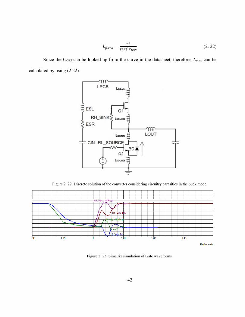
𝐿𝑝𝑎𝑟𝑎 =𝑇2
(2𝜋)2𝐶𝑂𝑆𝑆 (2. 22)
Since the COSS can be looked up from the curve in the datasheet, therefore, Lpara can be
calculated by using (2.22).
Figure 2. 22. Discrete solution of the converter considering circuitry parasitics in the buck mode.
Figure 2. 23. Simetrix simulation of Gate waveforms.

43
Figure 2. 23 shows the simetrix simulation of gate drive waveforms comparison. There is
a quite big delta between the actual waveform on the silicon die and the waveform on the
package. There is a shoot-through concern of LS bump back, as depicts in green curve, however,
the measurement result is misleading since it includes the parasitics and the real waveform on the
silicon die is very low, as depicts in blue curve, the peak of which is lower than the VGS(th) of LS
MOSFET.
Figure 2. 24. HS VDS waveforms comparison.
Figure 2. 24 shows the HS VDS waveform measured at the power pin (source) on the
package and at the silicon die as the arrows indicate. As depicted clearly in the fast acquisition
Measured at the silicon die
Measured at the package pin

44
scope shot, the true VDS is around 4V more than the result usually taken at the package. The
voltage delta is caused by the combination effect of fast di/dt and source clip inductance.
2.6 Efficiency Optimization
It is critical to optimize the static efficiency of power stage first since it is one of the key
performance metrics of the VR design. Load adaptive control (LAC) is proposed and
experimentally verified. The multiphase VR operation mode and phase number is the function of
the load current. FET drive voltage should also be adaptively adjusted to achieve the optimal
efficiency. Switch frequency, fSW, should be optimally chosen with nonlinear control loop
enabled so that the relatively low switching frequency would not impact the load transient
behavior.
Figure 2. 25. Light load CCM vs. PFM.

45
Figure 2. 25 shows the efficiency comparison at light load. PFM operation shows a big
advantage over CCM operation as expected and two curves are eventually converged at the load
which is around half of the inductor current ripple.
Figure 2. 26. Power loss reduction (PFM minus CCM) vs. VID.
Figure 2. 26 shows the power saving plot with increasing VOUT with 10mA of load
current. As the VOUT increases, it becomes more important to enable the VR working in the PFM
when the load current is small.
Converter parameters are in TABLE I, except for the disabled LL. VOUT is regulating at
1.05 V and measured at the output inductor. A GPIB based automated efficiency program, which
communicates to the data acquisition unit (Agilent 3497A) and electric load (Sorensen).is written
to record, VIN, IIN, VOUT, IOUT, VFET_DR, IFET_DR and plot the efficiency curve.
46
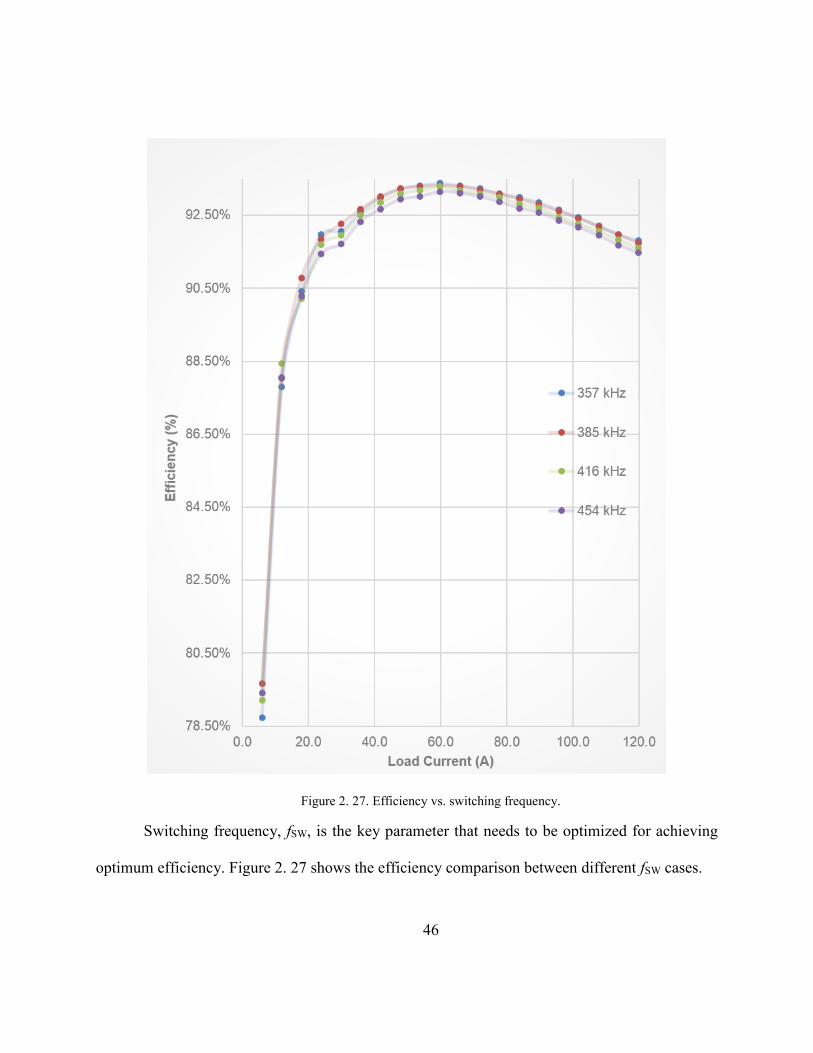
Figure 2. 27. Efficiency vs. switching frequency.
Switching frequency, fSW, is the key parameter that needs to be optimized for achieving
optimum efficiency. Figure 2. 27 shows the efficiency comparison between different fSW cases.

47
Figure 2. 28. Efficiency vs. FET drive voltage.
The driver voltage of power MOSFETs is also an important parameter to be optimized. In
the total power loss formula, it affects the Rdson of (2.6) and (2.14).

48
Figure 2. 29. Measured efficiency of multiphase buck converter with operating different number of phases.
Figure 2. 29 shows the measured efficiency plot of multiphase buck converter with
statically configured operation modes and different number of phases. There are in total seven
cases in this plot: one phase PFM and one to six phase CCM. The cross points between adjacent
phases operation can be programmed into the non-volatile memory (NVM) for this specific
power stage for auto phasing shedding purpose to flatten the efficiency curve over the entire load
range.

49
Power MOSFETs Selection
Switching Frequency Selection
MOSFET Drive Voltage Selection
Power Inductor Selection
Log Phase Current Threshold
Setup Simulation/Experimental with Initial
Converter Parameters
Efficiency Optimization with Load
Adaptive Control Reached
Figure 2. 30. Power efficiency optimization flow chart.
Table 2. 2 THE CONVERTER PARAMETERS
VBUS 12 V
VO 0.7 V~1.2 V
VFET_DRV 6.0 V
fSW
Loadline slope
385 kHz
0.8 mΩ
Output inductor per phase L = 230 nH
Output capacitor 6×470 µF Panasonic SP-Caps EEFSX0D471XE
44×22 µF MLCC

50
Figure 2. 31. Diagram of Load adaptive control.
Figure 2. 31 shows the diagram of load adaptive control based on previous optimization
results.
PWM6
PWM5
PWM4
PWM3
PWM2
PWM1
PFM
Load

51
CHAPTER THREE: LOW FREQUENCY TRANSIENT AND SYSTEM
DYNAMIC
In this chapter, load transient enhancement schemes are introduced for low frequency
transient operation. Adaptive body braking control is proposed to actively suppress the load
release. There is a consideration for dynamically adding and dropping phases so that the VOUT
excursion can be minimized. Load adaptive control has provided the benefit in power saving
perspective, however, it also creates a corner case scenario that shoot-through can be induced.
Hence, we propose a new dead-time management scheme incorporating both fixed and adaptive
dead-times so that the system reliability is secured and the power conversion efficiency during
normal operation is improved.
3.1 DCR Sense Network Impact
Accurate load current monitoring is an important feature and requirement in multiphase
converter design. The RC network across the definition points of the inductor can be
implemented to monitor the total phase current. The first design tuning in transient operation to
make the DCR sense match.
𝐿
𝐷𝐶𝑅= 𝑅𝐶 (3. 1)

52
Figure 3. 1. DCR sense network RC time constant.
In a pure voltage mode control with correct compensation as an optimization starting
point, Figure 3. 1 illustrates the VOUT impacted by the DCR sense network and the VOUT
excursions are color coded as blue, green and red. Green curve represents the ideal RC time
constant without nonlinear control enabled. If RC time constant is too large, as blue curve
indicates, VOUT is sluggish due to the delay in AVP loop and the overshoot can hurt the
reliability of CPU; if RC time constant is too small, as depicted in red curve, there will be a VOUT
sag during load insertion and the excessive undershoot can create a system hang in the
computing systems.
3.2 Nonlinear Control Scheme
In this section, control schemes are proposed and implemented to improve the system
dynamics during load transient operation.
Output voltage deviations or excursions that exceed the pre-defined window thresholds
are treated as load transient event [41] and a fast correction signal must be applied accordingly.
Without losing the benefit (high DC gain) of the voltage mode control during static operation,

53
the fast nonlinear loop includes a programmable multi-threshold window comparator, pulse
generation circuitry and interfacing circuitry to the normal PWM. When the sensed voltage is out
of the programmable window, the ATR asynchronously signals the modified PWM patterns for
compensating the output voltage. There are basically two types of asynchronous responses, i.e.
Active Load Release Response (ALRR) and Active Load Engage Response (ALER). The
nonlinear response essentially extends effective regulation bandwidth while maintain constant
output impedance over frequency. The red rectangles represent the time slot in each phase that
ALRR event can initiate. The orange and blue rectangles represent ALER event can be triggered
and they are threshold 1 and threshold 2, respectively. The internal counter module in each phase
is synchronous with switching frequency and points where the nonlinear events should be added.
For example in load engage event, the asynchronous pulses in each phase boost the switching
frequency to MHz range in the transient event, which effectively pumping the inductor current
energy to the output capacitance bank. The extra voltage generated by the nonlinear loop:
𝑉𝐸𝑋 =∑ ∫ 𝑖𝐿𝐾(𝑡+𝜃𝐾)𝑑𝑡𝑁𝐾=1
𝐶𝑂𝑈𝑇 (3. 2)
where iLK(t) represent the inductor ripple generated by the asynchronous pulse in phase K.
θK represents the phase angle difference between phase one. N presents the number of the active
phases. For simplicity COUT represent the total capacitance of bulk and ceramic caps.

54
Figure 3. 2. The ATR timing architecture of the multiphase controller.
AVP scheme is to maintain constant output impedance so that less output capacitors can
be populated and the output power of VR at full load can be reduced [1] -[5] . The nominal
loadline equation is mathematically expressed in (3.3) given system impedance (RLL):
𝑉𝑇𝑎𝑟𝑔𝑒𝑡 = 𝑉𝐼𝐷 − 𝐼𝐿𝑂𝐴𝐷 ∙ 𝑅𝐿𝐿 (3. 3)
3.2.1 Load Engage Enhancement
Nonlinear control scheme is a very critical technology and should be adopted in the slow
transient application (below 50 kHz). In VR application, nonlinear control schemes during load
engage transient event represent pulling-in PWM pulses or asserting PWM pulses faster than the
response from the linear loop. It reduces the voltage excursion and saves output capacitors.

55
Figure 3. 3 shows load engage response. The load current step is 131 A and the
associated slew rate is 524A/µs. The 6 digital channels represent 6 PWMs and the lighter blue is
the load current and darker blue is the voltage output.
Figure 3. 3. Load engage response with pure voltage mode control.
This is purely the voltage mode response and the 80 kHz control bandwidth can never
respond fast enough (fire the phases sooner rather than waiting the internal clock cycle) to
compensate the unwanted extra 60 mV undershoot. The ESR and ESL of the output caps are
causing the first sharp dip. Because the inductor current slew rate is far less than the slew rate of
output load current, due to the physics of the charge balance, the undershoot when load engage
can never be removed, but the undershoot can be improved if nonlinear control scheme can be
used.

56
Figure 3. 4. Load engage response w/ auto-phasing.
Figure 3. 4 depicts the load engage response of the multiphase buck converter with
ALER enabled. The same step and slew rate are adopted which are 131A and 524A/µs,
respectively. The 6 digital channels represent 6 PWMs and the cyan blue represents the load
current while darker blue represents the voltage output. Before the load is applied, it’s running
with 2 phase.
3.2.2 Load Release Enhancement
Existing methods for dealing with the overshoot voltage include increasing the output
capacitance of the VR to suppress the overshoot voltage, or “body braking” by using the body
diode of the power MOSFET in the VR to dissipate the excess current. Both options are
problematic, however, as large capacitors increase the cost and size of the VR and “body braking”

57
generates additional power loss and excess heat. Therefore, we propose a method to pulse the LS
gate ON and OFF to achieve the compromised result.
The equation set in (3.4) represents all operation scenarios or inductor current slopes in
the converter. Equation (a) represents the charging slope when converter is operating is the boost
(sink) mode with body diode of HS conducting. Equation (b) represents the charging slope when
converter is working is the buck mode. Equation (c) represents the discharging (freewheeling)
slope when LS is in asynchronous operation and body diode conducts (body braking). Equation
(d) represents the discharging slope when LS is turned on.
𝑖𝐿𝑠𝑙𝑒𝑤 =
{
𝑉𝐵𝑈𝑆 − 𝑉𝑂𝑈𝑇(𝑡) + 𝑉𝑆𝐷
𝐿 (𝑎)
𝑉𝐵𝑈𝑆 − 𝑉𝑂𝑈𝑇(𝑡)
𝐿 (𝑏)
−𝑉𝑂𝑈𝑇(𝑡) + 𝑉𝑆𝐷
𝐿 (𝑐)
−𝑉𝑂𝑈𝑇(𝑡)
𝐿 (𝑑)
(3. 4)
Figure 3. 5. Inductor current profile and gate-drive signals for the corresponding operations.

58
Figure 3. 5 depicts the all possible inductor current slopes or buck/boost mode from
equation (1) and corresponding gate-drive signals of synchronous and asynchronous operations.
Interval T1 and interval T2 represents HS body diode conducting and HS channel conducting,
respectively. Interval T3 and interval T4 represent asynchronous and synchronous rectifier control,
respectively.
Figure 3. 6. Load release response comparison.
As depicted in Figure 3. 6, the scope shot shows comparison effects of suppressing the
load release, which are the LS MOSFET ON, LS MOSFET OFF, and LS MOSFET Pulse control.
The colors of the waveforms are light blue, black and magenta, respectively. Overshoot = 58 mV
(Body diode ON). Overshoot = 68 mV (LS & Body diode ON).

59
Figure 3. 7. Inductor current slew rate difference during load release
Figure 3. 7 shows the resultant inductor current profiles during load release.
By using the pulse control of the LS during load release, the temperature is 7 degrees
lower than turning off the LS to freewheel the load current. Figure 3. 8 shows the inductor
current slopes difference when body diode ON, pulsing the LS and LS ON, respectively.
When a transient load such as a CPU operates in a large voltage range, the worst case
overshoot usually occurs at the lowest VID. Conventional body braking methods include turning
off the LS FET for either a whole cycle or a period of time targeting the lowest VID only.
Unfortunately, this braking method is typically too aggressive for higher VID levels. As a result,
power will be unnecessarily dissipated in body diode, which may also cause a thermal issue.
𝑖𝐿𝑠𝑙𝑒𝑤=𝑉𝑜𝑢𝑡(𝑡)+𝑉𝐷
𝐿
𝑖𝐿𝑠𝑙𝑒𝑤=𝑉𝑜𝑢𝑡(𝑡)
𝐿

60
Figure 3. 8. Adaptive body-braking control (pulsing control).
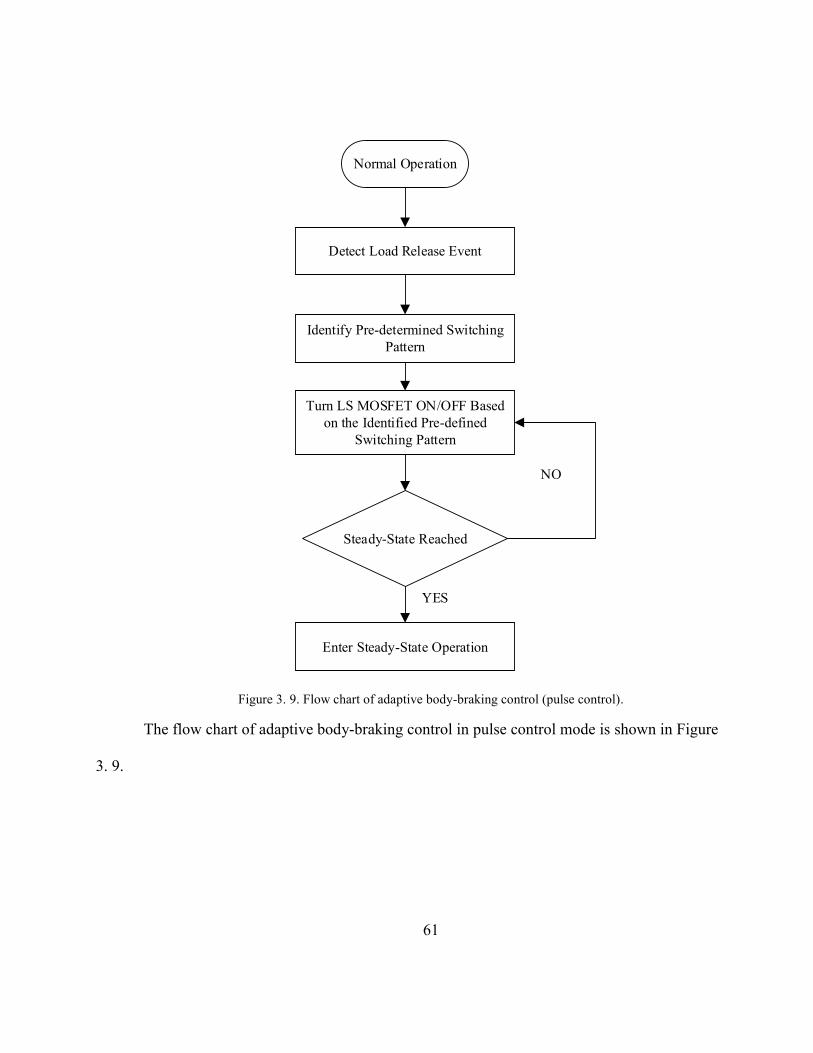
61
Normal Operation
Detect Load Release Event
Identify Pre-determined Switching
Pattern
Turn LS MOSFET ON/OFF Based
on the Identified Pre-defined
Switching Pattern
Steady-State Reached
Enter Steady-State Operation
NO
YES
Figure 3. 9. Flow chart of adaptive body-braking control (pulse control).
The flow chart of adaptive body-braking control in pulse control mode is shown in Figure
3. 9.

62
Figure 3. 10. Adaptive body-braking control (Body diode ON).
In Figure 3. 10, in body braking control duration, the pulse pattern is pulsing the LS gate,
but the duration of the OFF time is still adaptively changing according to the current VID, which
still based on the worst case overshoot in the lowest VID. Figure 3. 11 shows the related flow
chart.

63
Normal Operation
Detect Load Release Event
Turn OFF HS MOSFET
Turn ON LS MOSFET
Adaptive Turn OFF LS MOSFET
NO
YES
Re-enter Steady State Operation
Output Voltage Exceed Identified
Pre-determined Threshold
Figure 3. 11. Flow chart of adaptive body-braking control (Body diode ON).

64
3.3 Drop Phase Optimization
As analyzed in chapter 2, the phase number of the multiphase converter is the function of
load current and should follow adaptively with the load change from the static operation
perspective. However, there is extra care needs to be taken when shutting off the phase, which is
ramping down the inductor current before the drop operation.
Figure 3. 12. Overshoot during phase shedding.
Figure 3. 12 shows the phase shedding during load release. The yellow channel is VOUT.
The blue channel is load current. PWM2 and PWM3 are green and magenta channels
respectively. The load current step is 30A and slew rate is 10A/µs. There are three overshoots in
this scope shots circled in red. The first one is normal and is caused by the load step. The rest
overshoots are the result of dropping phase 2 and 3. When the two phases are turning off, the
corresponding phase still carries some current in the inductor. The turning OFF slew rate is

65
increased when the phase is off state because the current is freewheeling through the LS body
diode.
Once the phase dropping command is initiated, the state-machine of the current balance
module starts to modify the modulated ON time generated by PID and ramping down the
inductor current in the phase that is going to be turned off, meanwhile also increase the current in
other phase to take over the total load current. The overshoot caused by phase dropping can be
eliminated.
Figure 3. 13. Current balance block diagram.
The simulation shows the inductor current is ramping down 5 consecutive switching
cycles before the controller issue a drop commend.
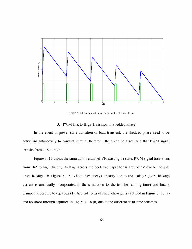
66
Figure 3. 14. Simulated inductor current with smooth gain.
3.4 PWM HiZ to High Transition in Shedded Phase
In the event of power state transition or load transient, the shedded phase need to be
active instantaneously to conduct current, therefore, there can be a scenario that PWM signal
transits from HiZ to high.
Figure 3. 15 shows the simulation results of VR existing tri-state. PWM signal transitions
from HiZ to high directly. Voltage across the bootstrap capacitor is around 3V due to the gate
drive leakage. In Figure 3. 15, Vboot_SW decays linearly due to the leakage (extra leakage
current is artificially incorporated in the simulation to shorten the running time) and finally
clamped according to equation (1). Around 13 ns of shoot-through is captured in Figure 3. 16 (a)
and no shoot-through captured in Figure 3. 16 (b) due to the different dead-time schemes.
0 1 2 3 4 5 6 7 8 9 100
2
4
6
8
10
12
t (uS)
Ind
ucto
r cu
rren
t (A
)

67
Figure 3. 15. Simulation results of VR entering tri-state.
(a)

68
(b)
Figure 3. 16. Simulation waveforms of existing long tri-state: (a) fixed dead-time: around 13 ns of shoot-
through (b) adaptive dead-time: No shoot-through captured.
There is no issue when VBOOT-SW is above 3.8 V, which presents the most operating
conditions. With lowering down PVCC and increased VOUT (around 1.8 V), there is a case that
driver can create a GH/GL overlap (shoot-through) scenario if the driver dead-time design is
fairly aggressive. When the dropped phase stays in tri-state in long period of time, the boot
capacitor is discharged by the gate driver leakage current (leakage rate: 1 nA/s), and eventually
VBOOT-SW is clamped depending on equation (1):
𝑉𝐵𝑂𝑂𝑇−𝑆𝑊 = 𝑃𝑉𝐶𝐶 − 𝑉𝑆𝐷 − 𝑉𝑂𝑈𝑇 (3. 5)
Where PVCC is the power MOSFET drive voltage. VSD is the diode voltage drop for the
internal switch.
As shown in Figure 2. 11, the level shift circuit takes the GND referenced signals and
level shift them to the HDRV “isolated” circuitry (level shift output) which is referenced to SW

69
node and powered from BOOT-SW capacitor voltage. The HS gate falling edge propagation
delay gets larger relative to LS rising edge delay. This BOOT-SW bleed depends on variables
such as VOUT and length on time in tri-state among other variables. The HS falling preparation
delay increase occurs regardless of PVCC voltage and can create a GH/GL overlap until BOOT
capacitor charges back up from the 2nd LS pulse.
As shown in Figure 3. 17(a), the red circle highlights the gates overlap when existing
long PWM tri-state. .The overlap is around 10 ns. As shown in Figure 3. 17(b) and (c). There are
several methods to eliminate the overlap. In Figure 3. 17(b), the PWM generate by the controller
should go to LOW first, which can charge up the voltage on BOOT capacitor, thus can shorten
the propagation delay and eliminate the shoot-through. In Figure 3. 17(c), the anti-shoot
protection unit directly monitors HG and LG, which can adaptively prevent the gate overlap
phenomenon in this specific scenario.
The avalanche breakdown energy of the power stage devices, from the worst case aspect,
is 50 mJ by Cadence Virtuoso Analog Design Environment simulation. The energy during the
gate overlap event is under 100 µJ, 1/500th the energy necessary for breakdown. However, from
the system robustness point of view, the gate overlap should be prohibited.

70
(a)
(b)

71
(c)
Figure 3. 17. Operational waveforms of existing long tri-state: (a) around 10 ns of shoot-through; (b) No shoot-
through captured by PWM going low first when exiting tri-state. (c) No shoot-through captured with “adaptive”
shoot-though protection.
This proposed method is to eliminate the shoot-through issue described above while still
maintaining efficient VR operation during steady-state operation mode. The proposed approach
combines advantages of both fixed dead-time and adaptive dead-time control methods.
The proposed dead-times management contains two sets of dead-times circuitries, i.e.
fixed dead-time and adaptive dead-time. Power conversion efficiency can be maximized due to
the shorter dead-times that can be implemented in steady-state mode. The adaptive dead-time can
be switched in when necessary to ensure the robustness of the power converter operation.
The adaptive dead-time control, which is adaptive to the manufacturing variation of Qg
and RG of the discrete MOSFETs, monitors the driver outputs, HDR and LDR. When the PWM

72
transitions to high, the LS gate voltage begins to fall after a propagation delay. At the same time,
LDR voltage is sensed, and high-side driving voltage starts to increase after LDR voltage is
lower than a proper threshold (1 V).
The fixed dead-time monitors the gate signals before level shift circuitry. Since the
MOSFET parameter variation is known and can be controlled, therefore a shorter (more
aggressive) delay can be asserted to achieve the fixed dead-time.
The efficiency improvement can be calculated based on the buck loss model. Reducing 5
ns more of both LS rising/falling dead-times translates to about 0.30% efficiency gain. For
example in mainstream application, there are totally 20 phases of multiphase VR in operation
and 1.23 W (12 phases of 2 Vcores: 0.66W, 8 phases of 4 MEM VRs: 0.57W) can be saved if the
dead-time can be shrunk by 5 ns given a general MOSFET usage.
𝑃𝑑𝑒𝑎𝑑𝑡𝑖𝑚𝑒 = 𝑉𝑆𝐷 ∙ 𝑓𝑆𝑊 ∙ [(𝐼𝑂𝑈𝑇 −𝐼𝑟𝑖𝑝𝑝𝑙𝑒
2) 𝑡𝑑𝑒𝑎𝑑𝑡𝑖𝑚𝑒(𝑟) + (𝐼𝑂𝑈𝑇 +
𝐼𝑟𝑖𝑝𝑝𝑙𝑒
2) 𝑡𝑑𝑒𝑎𝑑𝑡𝑖𝑚𝑒(𝑓)] 𝑁𝑝ℎ𝑎𝑠𝑒 (3. 6)
where tdeadtime(r) represents rising edge dead-time between LS turn off and HS turn on; tdeadtime(f)
represents rising edge dead-time between HS turn off and LS turn on; Nphase represents number of
active phases.

73
Driver POR and enabled
after 100 µs
Monitor input PWM logic
level
In tri-state for more than 100 µs
Switch dead-time management to adaptive
dead-time
Voltage on boot capacitor
reaches to Vcc
Switch dead-time management to
fixed dead-time
Reach 5 PWM
switching cycle
NO
YES
NO
NO
YESYES
Figure 3. 18. Dead-time management diagram when VR exist tri-state
Figure 3. 18 shows the proposed dead-time management scheme that can enhance the
system reliability and also maintain high power conversion efficiency.

74
CHAPTER FOUR: HIGH FREQUENCY TRANSIENT
High repetitive rate of load transient, especially the transient frequency at around
switching frequency, has been a challenge in power management industry [39] -[45] . Multiphase
buck converter suffers from the dynamic current sharing at this range of operation.
Voltage excursion generated by high frequency transient should be regulated within the
specification window. In voltage mode control, dynamic phase current imbalance is an expected
behavior and can be an issue, however, if it results in extra dynamic power loss, electrical or
thermal stress beyond the capability of the power component since the phase currents can sink
and source among phases. In this chapter, the high repetitive rate of load transient is explored.
We propose several methods to mitigate the issue so that the phase current can share better,
dynamic loss is therefore reduced and the system reliability in this operation mode is fully
enhanced.
4.1 Sampling Effects of PWM Converters
In voltage mode control, VCOMP, as illustrated in Figure 4. 1 (a), is the error amplifier
output and it compares with saw-tooth carrier signal to generate the PWM. As an illustration of
trailing-edge modulation in Figure 4. 1 (b), the perturbed VCOMP is introduced and PWM signal is
generated by the comparison between VCOMP and the saw-tooth carrier signal.

75
(a)
(b)
Figure 4. 1. PWM modulator diagram and VCOMP perturbation waveform: (a) PWM Modulator; (b)
modulation waveform with VCOMP perturbations.
Pulse width modulation (PWM) is a sampling hold system and it samples periodically at
the switching frequency where VCOMP and ΔOSC encounters.

76
The transfer function of zero-order hold is:
𝐻𝑍𝑂𝐻(𝑠) =1−𝑒−𝑆𝑇
𝑠 (4. 1)
(a)
(b)
Figure 4. 2. Frequency response of zero-order hold: (a) Gain; (b) Phase.
The transfer function of sample data system can be found as:
𝐻𝑍𝑂𝐻(𝑠) =1−𝑒−𝑆𝑇
𝑠𝑇 (4. 2)
Figure 4. 2 shows the frequency response of PWM sample data system. The sampling
frequency is 400 kHz as the simulation indicates.

77
4.2 Output Impedance Optimization
The output impedance design is a good measure of feedback loop characteristic.
According to CPU vendors’ requirements, a desired close loop ZOUT of the multiphase converter
should be constant across the full frequency range.
Figure 4. 3. Small-signal control block diagram of the closed loop output impedance.
𝐺𝑖𝑑(𝑠) =��𝐿(𝑠)
��(𝑠)|��𝑖𝑛(𝑠)=0��𝑜(𝑠)=0 =
𝑉𝑖𝑛
𝑠𝐿+𝑅𝐷𝐶𝑅+𝑅𝑂𝑈𝑇//(𝑅𝐸𝑆𝑅+1
𝑠𝐶𝑂𝑈𝑇) (4. 3)
𝑍𝑂(𝑠) =��𝑂(𝑠)
��𝑂(𝑠)|��𝑖𝑛(𝑠)=0��(𝑠)=0 =
𝑅𝐷𝐶𝑅(1+𝑠𝑅𝐸𝑆𝑅𝐶𝑂𝑈𝑇)(1+𝑠𝐿
𝑅𝐷𝐶𝑅)
𝑠2𝐿𝐶𝑂𝑈𝑇(𝑅𝐿𝑜𝑎𝑑+𝑅𝐸𝑆𝑅𝑅𝐿𝑜𝑎𝑑+𝑅𝐷𝐶𝑅
)+𝑠(𝐿
𝑅𝐿𝑜𝑎𝑑+𝑅𝐷𝐶𝑅+𝐶𝑂𝑈𝑇𝑅𝐸𝑆𝑅+𝑅𝐿𝑜𝑎𝑑//𝑅𝐷𝐶𝑅)+1
(4. 4)
𝐺𝑖𝑖(𝑠) =��𝐿(𝑠)
��𝑜(𝑠)|��𝑖𝑛(𝑠)=0��(𝑠)=0 =
1+𝑠𝑅𝐸𝑆𝑅𝐶𝑂𝑈𝑇
𝑠2𝐿𝐶𝑂𝑈𝑇(𝑅𝐿𝑜𝑎𝑑+𝑅𝐸𝑆𝑅𝑅𝐿𝑜𝑎𝑑+𝑅𝐷𝐶𝑅
)+𝑠(𝐿
𝑅𝐿𝑜𝑎𝑑+𝑅𝐷𝐶𝑅+𝐶𝑂𝑈𝑇𝑅𝐸𝑆𝑅+𝑅𝐿𝑜𝑎𝑑//𝑅𝐷𝐶𝑅)+1
(4. 5)

78
Gid is the transfer function of open loop duty cycle to inductor current.
ZO is the open loop output impedance.
Gii is the transfer function of open loop output current to inductor current.
GAVP is the AVP LPF transfer function.
GCOM is the total compensator gain.
As illustrated in Figure 4. 3, two transfer functions representing the loop gains, Ti(s) and
Tv(s) are defined as:
𝑇𝑣(𝑠) = 𝐺𝑣𝑑(𝑠) ∙ 𝐺𝑐𝑜𝑚(𝑠) (4. 6)
𝑇𝑖(𝑠) = 𝐺𝑖𝑑(𝑠) ∙ 𝐺𝑐𝑜𝑚(𝑠) ∙ 𝑅𝑑𝑟𝑜𝑜𝑝 ∙ 𝐺𝐴𝑉𝑃(𝑠) (4. 7)
By adopting Mason’s gain formula, the overall output impedance of voltage mode control
with AVP loop can be mathematically expressed as:
𝑍𝑂𝐶(𝑠) =𝑍𝑂(𝑠)(1+𝑇𝑖(𝑠))+𝐺𝑖𝑖(𝑠)𝐺𝑐𝑜𝑚(𝑠)𝑅𝑑𝑟𝑜𝑜𝑝𝐺𝐴𝑉𝑃(𝑠)𝑇𝑣(𝑠)
1+𝑇𝑖(𝑠)+𝑇𝑣(𝑠) (4. 8)
The output impedance and the compensation gain in high frequency region should be low
enough to attenuate high frequency noise.

79
Figure 4. 4. Plots of |Zv| and |ZOC|
4.3 Beat Frequency Mitigation
As repetitive load frequency is approaching switching frequency, the control loop cannot
respond fast enough to the load transient, as well as the current sharing loop. The dynamic
current between phases can sink and source and the dynamic loss increases due the extra
circulating energy. The extra phase imbalance current can also introduce extra stress on the
power devices. Therefore, there is a design mitigation need to be carried out.
The voltage loop BW is optimized to be 75 kHz, which is 1/5 of fSW as shown in this
work. Within the loop BW, feedback loop can maintain the stability of system. However, beyond
the loop BW, the compensator may not have good response to high frequency transient since the
loop gain is much damped. Moreover, it is prune to aliasing problem. So beyond the loop BW, it
is better to lower the impact of compensator and let the COUT handle the transient response.

80
In the event of low frequency load current transient, the control loop is optimized to
suppress load current changes so that the output impedance is controlled by the system’s closed
loop response. In the presence of high frequency, large load current change, the closed loop
response is optimized to minimize the peaking of the output impedance.
Load
Frequency
Detector
Nonlinear
Transient
Loop
Digital
PWMs
Vout
Vtarge
∑ VID
Adaptive
Voltage
Positioning
-
+
Differential
Current
Sense
PhaseCurrents
[1:6]Current
ADCs
Peak Current
Limiter
Digital
PID
DPWMs[1:Nphs]
EN
Voltage
ADC
∑ Verror
_
Figure 4. 5. Block diagram of load frequency detection (LFD).
Figure 4. 5 illustrates the simplified block diagram of the LFD scheme during high
frequency repetitive load transient. The programmable threshold should be bigger than the ripple
voltage. The polarity change rate in the voltage error indicates the load transient events: load
engage and load release. Once the detected load frequency surpassed the defined high frequency
range, the EN of nonlinear transient loop will be de-asserted. The current ADCs monitors the
phase current in the real time manner. The peak current limiter acts as a double layer protection
in the control loop that can truncate the PWM pulse once the sensed current is greater than the
threshold value. The inductor saturation can be eliminated and system reliability is enhanced. In

81
order to improve the reliability of the VR, the instantaneous phase current should be bounded.
The current protection in the control loop is proposed as a two layer function to mitigate the beat
frequency issue.
4.4 Dynamic Current Sharing
As shown in Figure 4. 6 (a), two cursors mark the total AC window for both overshoot
and undershoot excursions in low frequency transient. The extra undershoot caused by the beat
frequency oscillation in Figure 4. 6 (a), is not desirable and may cause blue screen in computing
systems. The beat frequency oscillation is eliminated by disabling the nonlinear loop. The VOUT
is regulated well within the AC window as illustrated in Figure 4. 6 (b).
(a)

82
(b)
Figure 4. 6. A load transient response. Load step: 10A-141A, slew rate: 450 A/µS. Rep rate: 400 kHz. (a)
Nonlinear loop enabled. (b) Nonlinear loop disabled.
Frequency domain analysis using Matlab is carried out and the effectiveness of the
proposed scheme is verified.
𝑉𝑜𝑢𝑡𝑘 = ∑ 𝑣𝑜𝑢𝑡𝑛𝑒−𝑖2𝜋𝑘𝑛
𝑁⁄
𝑁−1
𝑛=0
(4. 9)
Load rep rate is around 400 kHz, which is generated by Intel VRTT. The VOUT data are
the same as depicted in fig. 6 and are exported in DAT file from the scope. The spectral
characteristics of VOUT are informative. The low frequency peaking is around 9 kHz in Figure 4.
7 (a) with the nonlinear loop enabled. After disabling the nonlinear loop, as shown in Figure 4. 7
(b), the low frequency oscillation is removed and the only high magnitude in the spectrum
represents the load frequency.

83
(a)
(b)
Figure 4. 7. Magnitude of an N-point DFT on VOUT (high frequency rep rate transient). (a) Nonlinear
loop enabled. (b) Nonlinear loop disabled.

84
(a)
(b)
Figure 4. 8. Phase currents oscillation: transient step: 132A-165A, load frequency 385 kHz. (a) LFD
disabled. (b) LFD enabled.

85
Figure 4. 8 shows the improved phase currents screen captures by implementing the
proposed schemes. Magenta, cyan-blue and blue channels represent the 3 phase currents when
load frequency is 385 kHz, which is around switching frequency. Figure 4. 8 (a) shows the
circulating phase current among phases, the maximum sourcing and sinking current is 62A and -
24A, respectively. Phase currents were measured using proprietary fixture with BNC cables.

86
CHAPTER FIVE: DYNAMIC VOLTAGE SCALING
Dynamic voltage scaling is an energy saving feature in modern processors. The
multiphase VR design should have to facilitate CPUs to transit to the newer voltage level within
the specification with minimum power conversion.
Figure 5. 1. The impact of DVS operation at datacenter level.
Figure 5. 1 [46] shows the impact of DVS operation at datacenter level and shows the
significance of this operations.
5.1 Modes of Operation
In PFM, as shown in Figure 5. 2(b), PWM transitions from HiZ to high. Phase node
moves from output voltage level to VBUS. To achieve fast HiZ operation as depicted in Figure 5.
2 (b), EN toggle should be utilized in PFM operation. As the inductor current is reaching to zero,
the LS turns OFF. The output voltage then decays as a function of load. Power MOSFETs
remain HiZ until the output voltage drop below the regulation target to trigger a PWM on pulse.

87
(a) (b) (c)
Figure 5. 2. Operational waveforms with the critical dead times: (a) Buck (Source) CCM; (b) Buck (Source) PFM; (c)
Boost (Sink) Mode.
Under the boost mode, as shown in Figure 5. 2 (c), the phase node voltage is clamped to
VBUS plus a diode forward voltage drop after the HS MOSFET is OFF. The red rectangle
represents twatch-dog. LS MOSFET is hard switching after twatch-dog. After LS MOSFET turns on,
the current in the HS body diode commutates to the LS, going through the reverse recovery
phase.
Inductor current in one phase and the corresponding LS VDS waveform during mode
transition are shown in Figure 5. 3 LS VDS is starting negative because of the body diode voltage
drop during tdead−time. The edges in first VDS pulse are sharp due to COSS charges and discharges
very fast. After the tdead−time, LS is turning on the voltage drop on the VDS is RDS(on) multiplies
the inductor current. The falling edge of middle VDS pulse representing inductor equals to zero
and COSS discharges very slowly. In the last pulse, VDS is clamped to VIN plus diode forward
drop VSD during tdead−time and twatch-dog, respectively.
PWM
HGATE
LGATE
PHASE
PWM
HGATE
LGATE
PHASE
PWM
HGATE
LGATE
PHASE
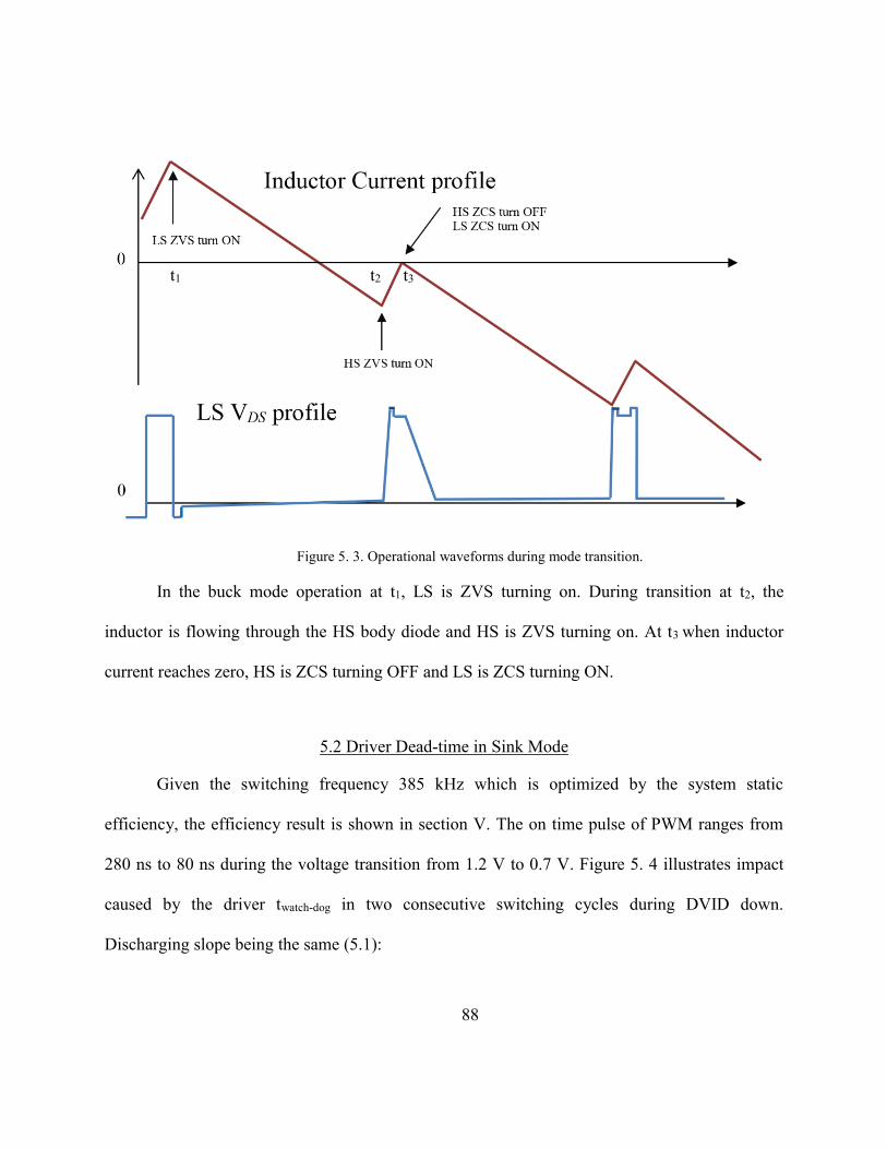
88
Figure 5. 3. Operational waveforms during mode transition.
In the buck mode operation at t1, LS is ZVS turning on. During transition at t2, the
inductor is flowing through the HS body diode and HS is ZVS turning on. At t3 when inductor
current reaches zero, HS is ZCS turning OFF and LS is ZCS turning ON.
5.2 Driver Dead-time in Sink Mode
Given the switching frequency 385 kHz which is optimized by the system static
efficiency, the efficiency result is shown in section V. The on time pulse of PWM ranges from
280 ns to 80 ns during the voltage transition from 1.2 V to 0.7 V. Figure 5. 4 illustrates impact
caused by the driver twatch-dog in two consecutive switching cycles during DVID down.
Discharging slope being the same (5.1):
t2 t1 t3

89
∆𝑖𝐿 =𝑉𝑂𝑈𝑇(𝜏)−𝑉𝑂𝑈𝑇(𝜏+∆𝑡)
2𝐿∆𝑡 (5. 1)
where ∆t represent the modulated OFF time or LS ON time between two switching cycles.
Inductor current 2 sank more when twatch-dog(red bar) is narrower, which effectively turns on the
LS2 sooner, therefore, the VOUT can be easily regulated and slewed down with respect to the
internal reference DAC.
Figure 5. 4. System dynamic comparison of different driver twatch-dog.

90
(a)
(b)
Figure 5. 5. Experimental waveforms with different design of twatch-dog: (a) Boost (Sink) mode: twatch-dog = 60
ns; (b) Boost (Sink) mode: twatch-dog = 120 ns.

91
Because the designed voltage mode controller will skip the PWM high pulse once the
sensed output is far beyond the reference DAC in the DVID downward operation. The prolonged
twatch-dog would cause essentially turning on the LS MOSFET of one phase asymmetrically,
therefore generate the unbalanced negative inductor current between phases. The MOSFETs and
VR long term reliability would degrade.
Figure 5. 5(a) illustrates the scenario of twatch-dog equals to 60 ns when the converter is
working in the boost mode (the output inductor current is negative). The driver actively sinks
current by “hard” turning on the LS MOSFET. Figure 5. 5(b) illustrates the scenario of twatch-dog
equals to 120 ns when the converter is in the DVID operation. The output inductor current
reaches zero, COSS of the LS MOSFET discharges and the driver waits for the phase node goes
low then turns on the LS MOSFET. The inductor energy is being discharged entirely back into
input capacitors. The extra 60 ns in twatch-dog introduce a delay in regulation which makes DVID
downward regulation very difficult.
5.3 Control MOSFET Stress Suppression
Repetitive avalanche can occur in the power MOSFETs in buck converters when the
voltage across the MOSFET exceeds the BVDSS voltage specified in the datasheet of the Power
MOSFET.
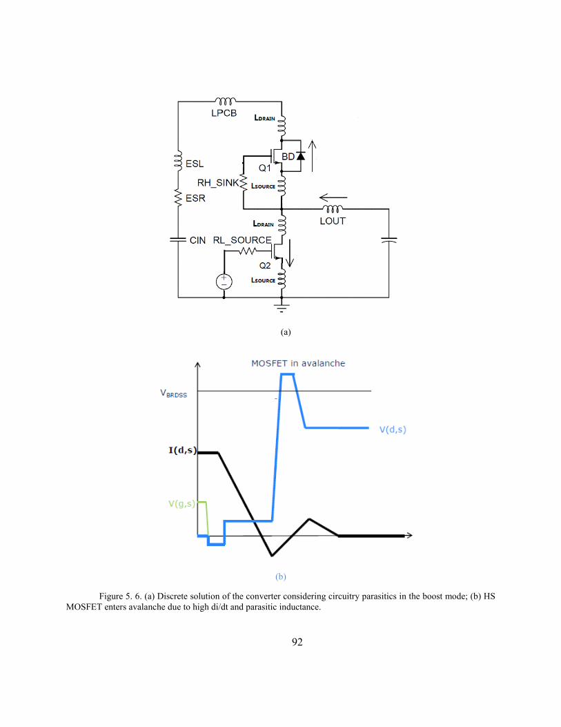
92
(a)
(b)
Figure 5. 6. (a) Discrete solution of the converter considering circuitry parasitics in the boost mode; (b) HS
MOSFET enters avalanche due to high di/dt and parasitic inductance.

93
The schematics of the discrete type of solution with circuitry parasitics are shown in Fig.
9 (a) when the converter is in the boost mode. The HS VDS can be mathematically expressed as:
dt
tdiLVtV D
STRAYBUSDS (5. 2)
where LSTRAY is loop parasitic inductance including LPCB, LDRAIN and LSOURCE. iD is the
diode reverse recovery current. A MOSFET spike approaching breakdown voltage level can
inflict high current transients on the MOSFET. While the body diode of HS MOSFET is
conducting current during the twatch-dog time slot, the diode PN junction are stored with minority
carriers.
Figure 5. 7. Equavelent circuitry with snubber when MOSFET is in off state.
Figure 5. 7 shows the equivalent circuitry with snubber circuit when MOSFET is in off
state. CGFP is formed by gate electrode, interelectrode and field electrode. Rfp is the field-

94
electrode resistance between source terminal and field electrode. Fine tune the snubber resister,
Rfp, is very critical in the MOSFET design to surpress the VDS ringing.
Figure 5. 8. Simulation result of HS VDS waveforms with different snuber resister Rfp.
Figure 5. 8 shows the Simetrix simulation result of the damping effect of HS VDS
waveforms by varying RFP resistance. The snubber resister cannot be too large, as the blue curve
indicates, which produces a shoot-through condition and degrades the system reliability and
efficiency. Likewise, the resistance cannot be too small, which indicates the avalanche syptom. 3
Ohm can be chosen as a optimal value for the snubber circuitry.
In Figure 5. 9, the screen capture shows the HS VDS during the fast DVID (a) 20 mV/µs
and (b) 40 mV/µs down in the fast acquisition mode. The maximum amplitude of VDS in Figure
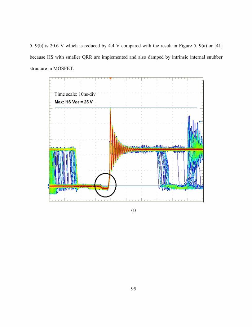
95
5. 9(b) is 20.6 V which is reduced by 4.4 V compared with the result in Figure 5. 9(a) or [41]
because HS with smaller QRR are implemented and also damped by intrinsic internal snubber
structure in MOSFET.
(a)
Time scale: 10ns/div

96
(b)
Figure 5. 9. High side VDS during repetitive DVID operation: (a) QRR = 20 nC and without snubber
circuitry; (b) QRR= 10 nC with snubber circuitry. Channel 2: HS drain-source voltage, 5V/div.
During DVID downward transition, the inductor current is flowing reversely because the
energy stored in the cap banks dumps back to the input side. The circled area shows when HS
turned off and body diode of HS is conducting. The excessive spike on VDS may lead to impact
ionization and avalanche of the MOSFET. According to simulation and experimental verification,
there are three ways to reduce the ringing on VDS:
Embed and fine tune the internal snubber structure;
Embed one more layer of Schottky barrier diode in the HS MOSFET design,
which essentially reduces QRR;
Use integrated power stage, such as stacked-die package, which reduces the
parasitic inductance.
Time scale: 10 ns/div

97
5.4 DVS Responsiveness Optimization
The voltage transition during dynamic voltage scaling should meet the timing and voltage
excursion requirements of the specific CPU application. Nonlinear control scheme and Cdv/dt
compensation are introduced to fulfill the smoothness of this dynamic transition.
5.4.1 Nonlinear Control Scheme
Figure 5. 10. The timing architecture of the multiphase controller.
Figure 5. 10 shows the timing architecture of the multiphase VR. It is not only useful for
dealing with low frequency load transient, it can help smooth the voltage output during DVID
operation, especially during DVID downward transition.

98
5.4.2 CdV/dt Compensation
AVP is an advantageous technique for load transient events. The AVP loop, however,
should be carefully examined in the DVID design. It uses the total inductor current to represent
the load current, however, during VID changes, even though the load current stays constant,
there is amount of phase current, CdV/dt current to charge or discharge the output capacitors.
The extra amount of total inductor current is in the closed loop that can affect the VOUT
regulation target according to (4). The AVP loop creates a lag and slows the VOUT settling in
DVID upward transition. The slow settling generates the issue for Alert timing in the sVID bus if
the stringent timing is required in the processor application.
VID VID
Ramp
Generator
OFFSET
Compensation
C dV/dt
Compensation
+Isense(total current)
AVP
Compensation +Vtarget
-
-
Current
Compensation Voltage
Compensation
∑
CH1
CH2
.
.
.
CHN
Phase1
Phase2...
PhaseN
Anti-alias
Filter
+ADCPIDPWMLoad
Model-
Figure 5. 11. Architecture of DVID module with compensations.
Figure 5. 11 illustrated the architecture of DVID compensation in both current and
voltage aspects. It is very critical for compensating the droop current, the current for charging the
output capacitors during dynamic operation and thus catching the timing of DVID upward
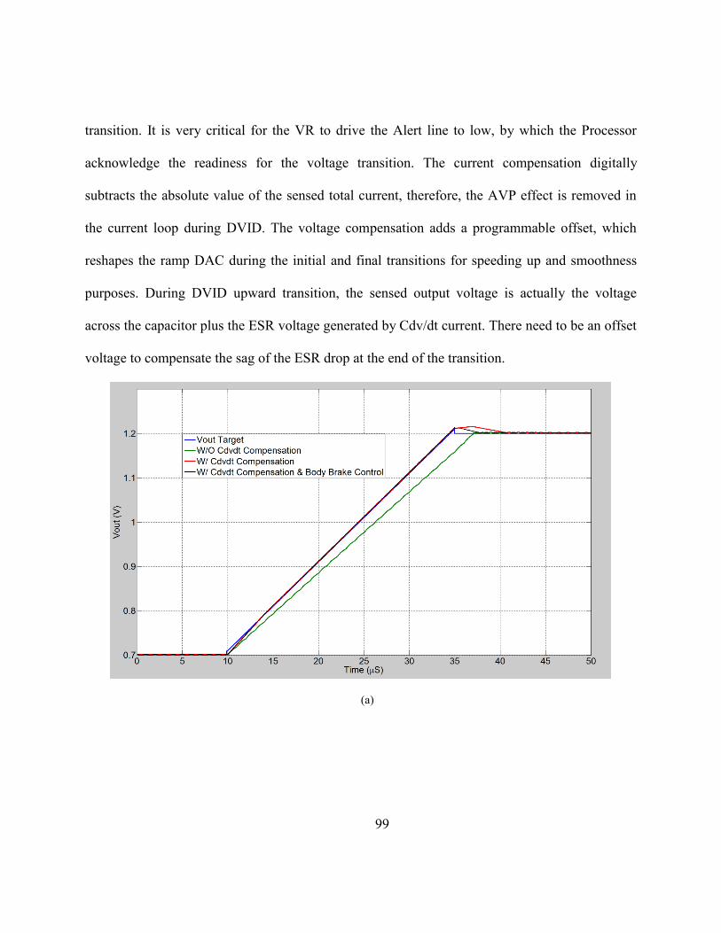
99
transition. It is very critical for the VR to drive the Alert line to low, by which the Processor
acknowledge the readiness for the voltage transition. The current compensation digitally
subtracts the absolute value of the sensed total current, therefore, the AVP effect is removed in
the current loop during DVID. The voltage compensation adds a programmable offset, which
reshapes the ramp DAC during the initial and final transitions for speeding up and smoothness
purposes. During DVID upward transition, the sensed output voltage is actually the voltage
across the capacitor plus the ESR voltage generated by Cdv/dt current. There need to be an offset
voltage to compensate the sag of the ESR drop at the end of the transition.
(a)

100
(b)
Figure 5. 12. Matlab simulation result of DVID transition with and without droop compensation and
nonlinear control: (a) DVID upward transition; (b) DVID downward transition.
DVID transitions are simulated using Matlab and presented in Figure 5. 12. The VOUT
with CdV/dt compensation (red and black curves), in Figure 5. 12 (a) was regulated tightly to the
VTarget. Body brake control can further reduce the overshoot during DVID upward transition as
indicated in the black curve. As shown in Figure 5. 12 (b), the reshaped VTarget with Cdv/dt
compensation can bring in extra asynchronous pulses at the end of the transition to ensure no
undershoot occurs.
Figure 5. 13(a) and (b) show experimental waveforms of fast DVID transition with
CdV/dt compensation (Cyan) and without the compensation (Black). Six digital channels in the
scope shots represent the six PWM signals of the VR.
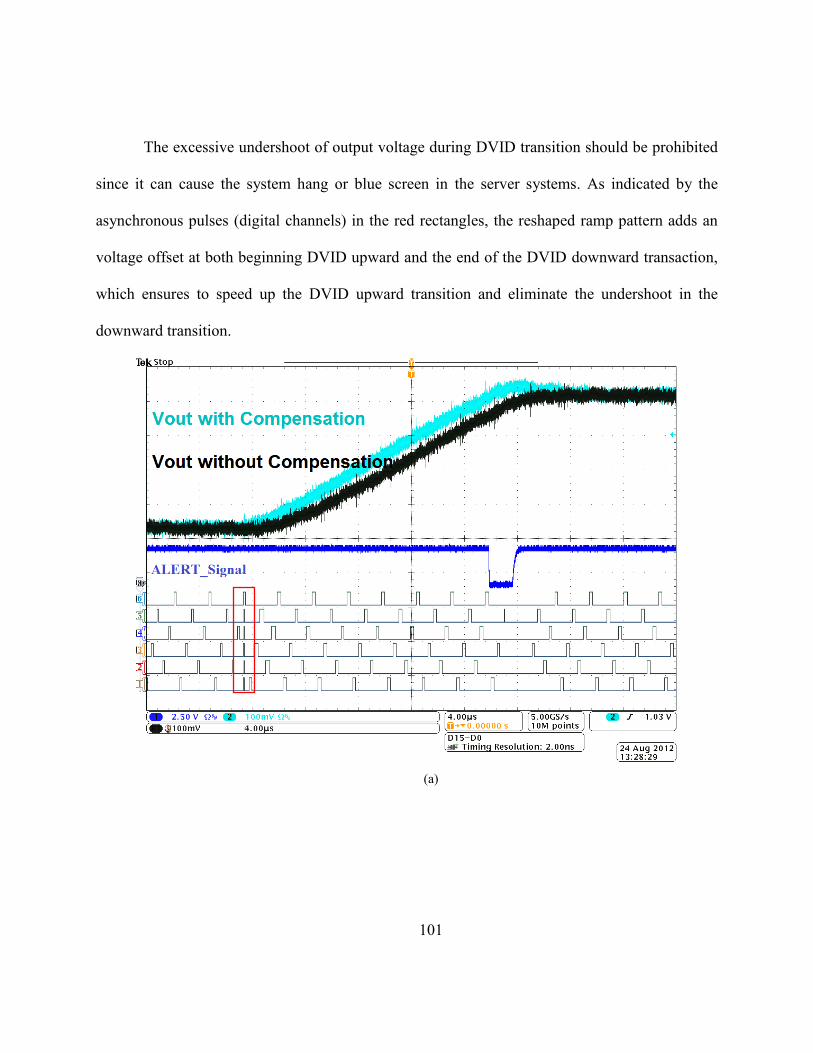
101
The excessive undershoot of output voltage during DVID transition should be prohibited
since it can cause the system hang or blue screen in the server systems. As indicated by the
asynchronous pulses (digital channels) in the red rectangles, the reshaped ramp pattern adds an
voltage offset at both beginning DVID upward and the end of the DVID downward transaction,
which ensures to speed up the DVID upward transition and eliminate the undershoot in the
downward transition.
(a)

102
(b)
Figure 5. 13. Experimental waveforms of fast DVID transitions with/without C·dV/dt compensation: (a) Fast DVID
upward transition; (b) Fast DVID downward transition.
Given the total output capacitance CO, the relationship between the sinking/sourcing
current and DVID slew rate can be expressed by:
𝐼𝑠𝑖𝑛𝑘/𝑠𝑜𝑢𝑟𝑐𝑒 = 𝐶𝑂𝑑𝑉
𝑑𝑡 (5. 3)
Server processors roughly have about 4000 µF of CO in each VR. At 20mV/µs DVID rate:
80 Amps of source or sink current during DVID.

103
5.4 Current Sharing during DVS
In order to ramp up or down the voltage on the output capacitor according to the sVID
transactions, an extra amount of phase currents need to charge or discharge the output capacitors.
The phase current during transitions, especially DVID downward operation, should be shared
evenly among the active phases.
(a)

104
(b)
Figure 5. 14. Simulation result of total phase current. (a) Source current at different VID transition. (b) Sink
current at different VID transition.
Figure 5. 14 shows the simulation results of total charge and discharge phase current
during 3 different VID transition, which are 1.2V-0.7V (in blue), 1.2V-0.9V(in red) and 1.2V-
1.1V(in green), respectively. As the equation (5.3) indicates, the VID delta represents different
sink/source energy. Figure 5. 14 (b) can enforce the VR in sink (boost) mode, so the inductor
current flows reversely and the negative current need to be shared during this operation. As it has
been discussed in the previous section that twatch-dog is an important IC parameter that need to be
optimized. If the value is too big, the controller can turn on the LS asymmetrically and the phase
current cannot be shared evenly among phases since during this operation, the priority operation
of the controller is to ramp down the VOUT in a controlled fashion.

105
Figure 5. 15. Negative current calculation in DVID downward transition.
The worst case negative current in one phase can be calculated by measuring the time and
applies to the corresponding slope section in this illustration. There are totally three inductor
current slopes, which are HS ON slope1, HS body diode ON slope 2 and LS ON slope3. And we
know this happens at the end the very end of downward transition, so we assume the VOUT equals
to 0.7V. . And the inductance we assume not varied with load
𝑃𝑖𝑛𝑑𝑢𝑐𝑒𝑑_𝑙𝑜𝑠𝑠 = (𝐸𝑐𝑜𝑛𝑑𝑢𝑐𝑡𝑖𝑜𝑛 + 𝐸𝐴𝑣𝑎𝑙𝑎𝑛𝑐ℎ𝑒∗) × 𝑓𝑟𝑒𝑝_𝑟𝑎𝑡𝑒 (5. 4)
*: if there is avalanche.

106
(a)
(b)
Figure 5. 16. Vout regulation comparison of different driver twatch-dog during DVID down.
(a) Sink mode: twatch-dog =120 ns; (b) Sink mode: twatch-dog = 60. ns.

107
In order to accomplish the DVID downward operation in the controlled fashion, the
energy stored in the output capacitor must be discharged. The phase current must sink fast
enough to regulate down the voltage.
5.5 Phase Number Control during DVS Operation
In dynamic voltage operation, the phase number should also be optimized when VID
transits, but as the function of VID delta. As discussed in previous section, there are two
operation modes, i.e. buck and boost, respectively. The switching characteristics are shown in
Table 5. 1.
TABLE 5. 1 SWITCHING CHARACTERISTICS
HS LS
Buck mode “Hard” switching “Soft” switching
Boost mode “Soft” switching “Hard” switching
TABLE 5. 2 MOSFET CHARACTERISTICS
HS
(BSZ036NE2LS)
LS
(BSC014NE2LSI)
Rds_on (mΩ) 3.6 1.4
Rg (Ω) 0.9 0.6
Qgs (nC) 3.1 7
Qgd (nC) 1.9 7
Qg(nC) 7.7 19
QRR (nC) 10 5
QOSS(nC) 9.4 25
Table 5. 2 shows the MOSFETs employed in the experiment, including static, gate charge
and reverse recovery characteristics.
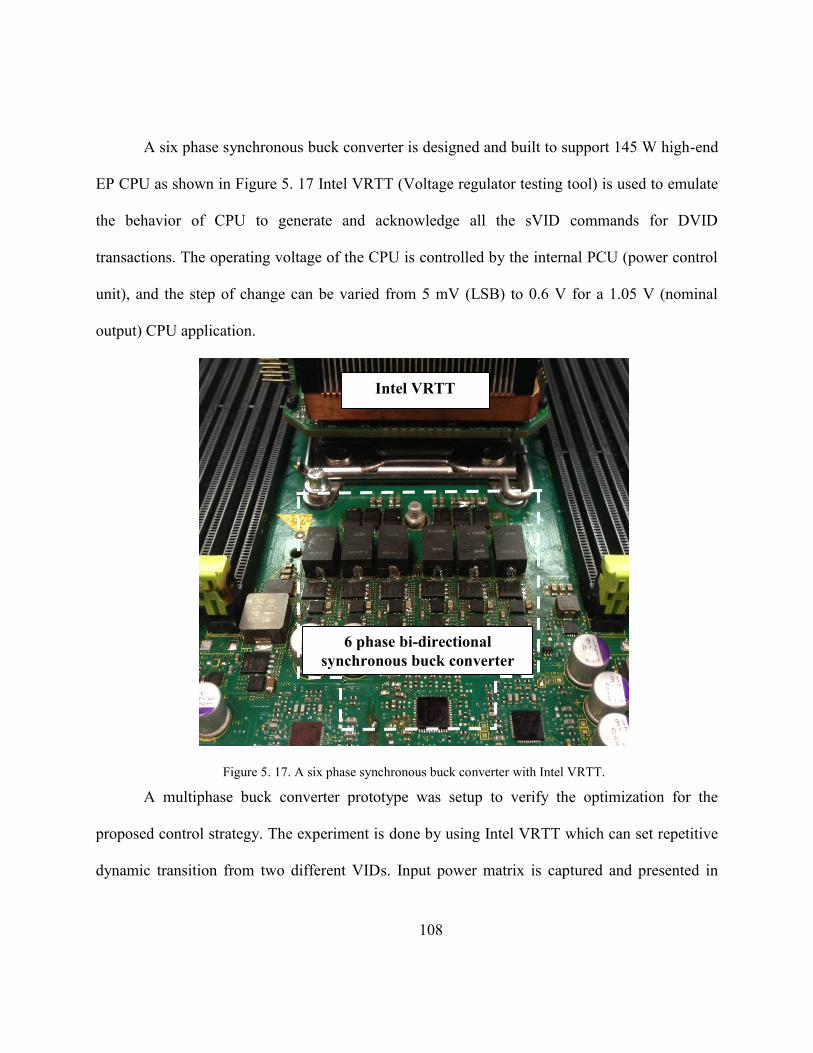
108
A six phase synchronous buck converter is designed and built to support 145 W high-end
EP CPU as shown in Figure 5. 17 Intel VRTT (Voltage regulator testing tool) is used to emulate
the behavior of CPU to generate and acknowledge all the sVID commands for DVID
transactions. The operating voltage of the CPU is controlled by the internal PCU (power control
unit), and the step of change can be varied from 5 mV (LSB) to 0.6 V for a 1.05 V (nominal
output) CPU application.
Figure 5. 17. A six phase synchronous buck converter with Intel VRTT.
A multiphase buck converter prototype was setup to verify the optimization for the
proposed control strategy. The experiment is done by using Intel VRTT which can set repetitive
dynamic transition from two different VIDs. Input power matrix is captured and presented in
6 phase bi-directional
synchronous buck converter
Intel VRTT
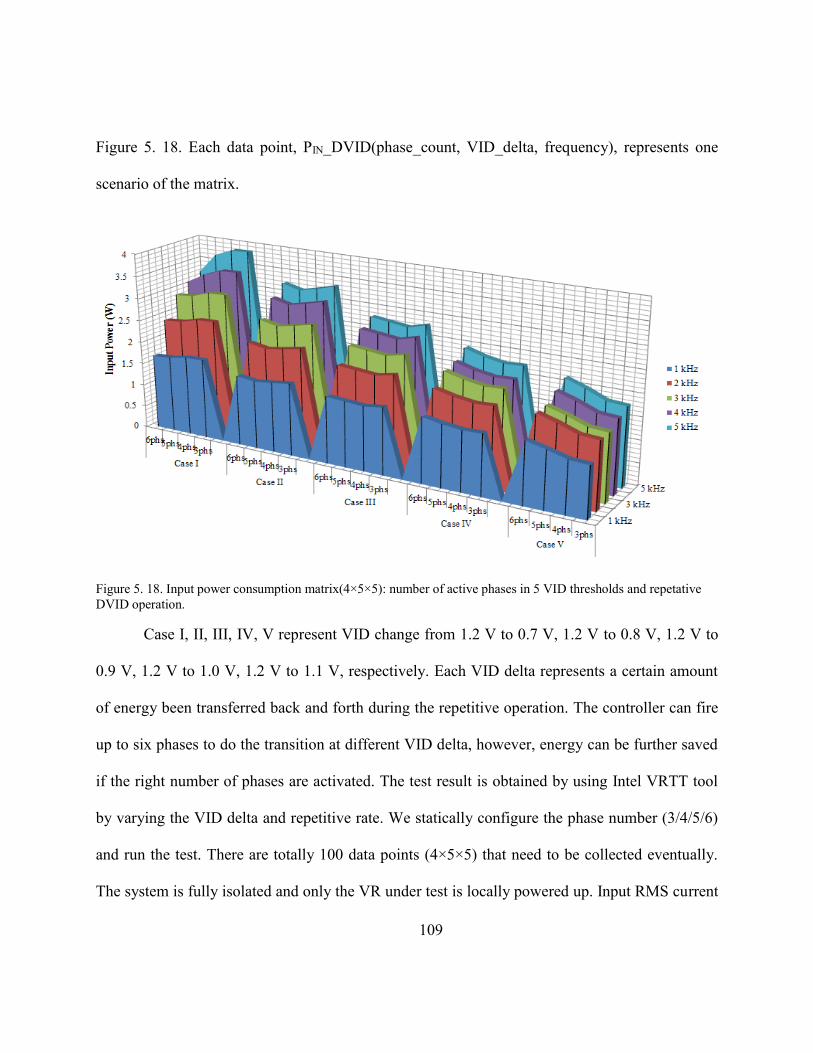
109
Figure 5. 18. Each data point, PIN_DVID(phase_count, VID_delta, frequency), represents one
scenario of the matrix.
Figure 5. 18. Input power consumption matrix(4×5×5): number of active phases in 5 VID thresholds and repetative
DVID operation.
Case I, II, III, IV, V represent VID change from 1.2 V to 0.7 V, 1.2 V to 0.8 V, 1.2 V to
0.9 V, 1.2 V to 1.0 V, 1.2 V to 1.1 V, respectively. Each VID delta represents a certain amount
of energy been transferred back and forth during the repetitive operation. The controller can fire
up to six phases to do the transition at different VID delta, however, energy can be further saved
if the right number of phases are activated. The test result is obtained by using Intel VRTT tool
by varying the VID delta and repetitive rate. We statically configure the phase number (3/4/5/6)
and run the test. There are totally 100 data points (4×5×5) that need to be collected eventually.
The system is fully isolated and only the VR under test is locally powered up. Input RMS current

110
is obtained using data acquisition unit to compare the different power consumption. Repetitive
DVID frequency is color coded and ranges from 1 kHz to 5 kHz, as shown in Figure 5. 19.
Active phase count is labeled in each test case. From the experiment results, case 1 and case 2 we
can program 6 phases to run, even 4 phases may save certain power, but the stress (especially,
HS VDS) on the device is much higher. From the power saving standpoint, case 3 and case 4 can
be using 5 phases, and 4 phases, respectively. Case 5 represents lowest VID delta in this
experiment, 3 phases will be sufficient and 300 mW can be saved compared to firing 6 phases.
Figure 5. 19. Phase number control based on VID delta.

111
When the output voltage transits from one VID to another VID, number of active phases
should be added or shedded to minimize the power loss based on VID delta, as shown in Figure
5. 19.

112
CHAPTER SIX: CONCLUSIONS AND FUTURE WORK
In this dissertation, comprehensive investigations and optimizations on multiphase
synchronous buck converter are presented. The optimization is focused on the real system
running condition and corner case scenarios.
6.1 Major Contributions
The major contributions of this work are listed in below.
We investigate the power conversion loss in all CPU VR operating conditions, carry out
the efficiency optimization by parametric variation and propose load adaptive control scheme.
Driver interface is thoroughly investigated for operation and efficiency purposes. Switching
waveforms are understood better with incorporating all the parasitics.
We propose the load transient enhancement schemes to minimize the output voltage
excursion during low frequency load transient. During load engage, the pulse should be pulled in
fast enough to compensate the voltage deviation. During load release, adaptive body braking
schemes are proposed to adaptively suppress the voltage overshoot. A true system operation
scenario that can create power MOSFETs shoot-through is captured and new dead-time
management scheme is proposed to maintain the high efficiency and ensure the system reliability.
In the presence of large, high frequency load current change, the closed loop response is
optimized to minimize the peaking of the output impedance. The small signal closed loop system
output impedance is derived and the PID values are optimized in the high frequency range to
attenuate the high frequency system noise. Beat frequency is studied and mitigated by the

113
proposed load frequency detection scheme by turning OFF the nonlinear loop and introducing
current protection in the control loop.
We present the detailed design considerations for multiphase converter running in
dynamic voltage scaling (DVS). Optimized driver dead-time in boost mode operation are
illustrated and DVID downward transition can be achieved with negative current shared among
phases. The excessive stress on the control MOSFET which increases the reliability concern is
captured in boost mode operation. Feasible solutions are also proposed and verified by both
simulation and experiment results. CdV/dt compensation for removing the AVP effect and novel
nonlinear control scheme for smooth transition are proposed for dealing with fast voltage
positioning. Optimum phase number control during dynamic voltage transition is also proposed
and triggered by voltage identification (VID) delta to further reduce the dynamic loss.
6.2 Future Works
System integration is the trend of power related design. Discrete power MOSFETs and
drivers can be designed and manufactured into the same package to minimize the footprint and
ringing. Driver dead-time can be further optimized since the MOSFET parameters and parasitics
are known in a defined range.
Efficiency optimization can be further carried out by using inductor with ultra-low DCR.
Since the SNR is too low that controller cannot handle. The current sense architecture, therefore,
needs to be redesigned. MOSFET current sense, with built-in current mirror, can be adopted and
characterized to solve the above issue.

114
LIST OF REFERENCES
[1] IMS Research, available at http://www.imsresearch.com/
[2] Intel document, “Voltage Regulator Module (VRM) and Enterprise Voltage Regulator-Down
(EVRD) 12.0” April 2010, available at http://www.intel.com
[3] A. Waizman and C.-Y. Chung,“Resonant free power network design using extended adaptive
voltage positioning (EAVP) methodology,” IEEE Trans. Adv. Packag., vol. 24, no. 3, pp.
236–244, Aug. 2001.
[4] K. Yao, M. Xu, Y. Meng, and F. C. Lee, “Design considerations for VRM transient response
based on the output impedance,” IEEE Trans. Power Electron., vol. 18, no. 6, pp. 1270-1277,
Nov. 2003.
[5] S. Pan; P.K.; Jain, "A New Digital Adaptive Voltage Positioning Technique with
Dynamically Varying Voltage and Current References," IEEE Trans., Power Electron.,
vol.24, no.11, pp.2612-2624, Nov. 2009
[6] M. Lee, D. Chen, K. Huang, C. Liu, and B. Tai, “Modeling and design for a novel adaptive
voltage positioning (AVP) scheme for multiphase VRMs,” IEEE Trans. Power Electron.,
vol. 23, no. 4, pp. 1733-1832, Jul. 2008.
[7] R. Erickson and D. Maksimovic. “Fundamentals of power electronics.” Springer, 2001.
[8] G. Franklin, M. Workman, and D. Powell. “Digital control of dynamic systems.” Addison-
Wesley Longman Publishing Co., Inc., 1997
[9] K. Ogata and Y.Yang, “Modern control engineering,” 5/5, Prentice Hall, 2010.
[10] Matlab Control System Toolbox, available at http://www.mathworks.com/help/control/
[11] J. Proakis, and D. Manolakis, “Digital Signal Processing: Principles, Algorithms, and
Applications,” 4/e. Pearson Education, 2007.
[12] B.J. Patella, A. Prodic, A. Zirger, D. Maksimovic, "High-frequency digital PWM controller
IC for DC-DC converters," IEEE Trans. Power Electron., vol.18, no.1, pp.438,446, Jan 2003
[13] J. Li, F.C. Lee, "Modeling of V2 Current-Mode Control," IEEE Trans. Circuits Syst. I, Reg.
Papers, vol.57, no.9, pp.2552-2563, Sept. 2010.
[14] J. Li, F.C. Lee, "New Modeling Approach and Equivalent Circuit Representation for Current-
Mode Control," IEEE Trans. Power Electron., vol.25, no.5, pp.1218-1230, May 2010.
115
[15] J. Fan; X. Li; S. Lim; A.Q. Huang, "Design and Characterization of Differentially Enhanced
Duty Ripple Control (DE-DRC) for Step-Down Converter," IEEE Trans., Power Electron.,
vol.24, no.12, pp.2714-2725, Dec. 2009
[16] F. Ma; W. Chen; J. Wu; "A Monolithic Current-Mode Buck Converter With Advanced
Control and Protection Circuits," IEEE Trans. Power Electron., , vol.22, no.5, pp.1836-1846,
Sept. 2007
[17] S.C. Huerta, A. Soto, P. Alou,; J.A. Oliver, O. Garcia, J.A. Cobos, "Advanced Control for
Very Fast DC-DC Converters Based on Hysteresis of the Current," IEEE Trans. Circuits
Syst. I: Reg. Papers, vol.60, no.4, pp.1052,1061, April 2013
[18] K. Lee, F. Lee, and M. Xu, “A Hysteretic Control Method for Multiphase Voltage
Regulator,” IEEE Trans. Power Electron., vol. 24, no. 12, pp. 2726–2734, Dec. 2009.
[19] Texas Instrument TPS53819, available at http://www.ti.com/
[20] Texas Instrument TPS51622, available at http://www.ti.com/
[21] Intersil ISL6363 datasheet, available at http://www.intersil.com/
[22] Intersil ISL95210 datasheet, available at http://www.intersil.com/
[23] Intersil ISL6364 datasheet, available at http://www.intersil.com/
[24] W. Qiu; G. Miller, Z. Liang, "Dual-Edge Pulse Width Modulation Scheme for Fast Transient
Response of Multiple-Phase Voltage Regulators," in Proc IEEE PESC, Jun. 2007 pp.1563-
1569
[25] S. Xiao, W. Qiu, G.Miller, T. X.Wu, I.Batarseh, "Adaptive Modulation Control for Multiple-
Phase Voltage Regulators," IEEE Trans. Power Electron., vol.23, no.1, pp.495,499, Jan.
2008
[26] W. Qiu, C. Cheung, S. Xiao and G. Miller, "Power Loss Analyses for Dynamic Phase
Number Control in Multiphase Voltage Regulators," in Proc. IEEE APEC, 2009, pp.102-108.
[27] Y. Ren, M. Xu, J. Zhou and F. C. Lee, “Analytical loss model of power MOSFET,” IEEE
Trans. Power Electron., vol. 21, no. 2, pp. 310–319,Mar. 2006.
[28] Z. J. Shen, D. N. Okada, F. Lin, S. Anderson and C. Xu, “Lateral power MOSFET for
megahertz-frequency, high-density DC/DC converters,” IEEE Trans. Power Electron., vol. 21,
no. 1, pp. 11–17, Jan. 2006.

116
[29] Y. Xiong; S. Sun; H. Jia; P. Shea; Z. J Shen, “New Physical Insights on Power MOSFET
Switching Losses,” IEEE Trans., Power Electron., vol.24, no.2, pp.525-531, Feb. 2009
[30] W. Qiu, S. Mercer, Z. Liang and G. Miller , "Driver Deadtime Control and Its Impact on
System Stability of Synchronous Buck Voltage Regulator," IEEE Trans. Power Electron.,
vol.23, no.1, pp.163-171, Jan. 2008.
[31] D. Disney, Z. J. Shen, "Review of Silicon Power Semiconductor Technologies for Power
Supply on Chip and Power Supply in Package Applications," IEEE Trans,Power Electron.,
vol.28, no.9, pp.4168-4181, Sept. 2013
[32] Q. Zhao; G. Stojcic, "Characterization of Cdv/dt Induced Power Loss in Synchronous Buck
DC–DC Converters," IEEE Trans. Power Electron., vol.22, no.4, pp.1508,1513, July 2007
[33] W. Eberle, ,Z Zhang, Y Liu, P.C. Sen, "A Current Source Gate Driver Achieving Switching
Loss Savings and Gate Energy Recovery at 1-MHz," IEEE Trans.Power Electron., pp 678 -
691 Volume: 23, Issue: 2, March 2008.
[34] W. Eberle, Y. Liu; P.C. Sen, "A New Resonant Gate-Drive Circuit With Efficient Energy
Recovery and Low Conduction Loss," IEEE Trans. Ind. Electron., vol.55, no.5, pp.2213-
2221, May 2008.
[35] Z. Zhang; W. Eberle,; Z. Yang; Y. Liu; P.C. Sen, "Optimal Design of Resonant Gate Driver
for Buck Converter Based on a New Analytical Loss Model," IEEE Trans Power Electron.,
vol.23, no.2, pp.653-666, March 2008.
[36] X. Zhou; M. Donati, L. Amoroso; F.C., Lee, "Improved light-load efficiency for synchronous
rectifier voltage regulator module," IEEE Trans Power Electron., vol.15, no.5, pp.826,834,
Sep 2000.
[37] Julu Sun; Ming Xu; Yuancheng Ren; Lee, F.C., "Light-Load Efficiency Improvement for
Buck Voltage Regulators," IEEE Trans Power Electron., vol.24, no.3, pp.742-751, March
2009.
[38] J. Su; C. Liu, "A Novel Phase-Shedding Control Scheme for Improved Light Load Efficiency
of Multiphase Interleaved DC–DC Converters," IEEE Trans Power Electron., vol.28, no.10,
pp.4742-4752, Oct. 2013
[39] A. Costabeber, P. Mattavelli and S. Saggini, "Digital Time-Optimal Phase Shedding in
Multiphase Buck Converters," IEEE Trans. Power Electron., vol.25, no.9, pp.2242-2247,
Sept. 2010

117
[40] Y. Qiu, M. Xu, K. Yao, J. Sun, and F.C. Lee, "Multifrequency Small-Signal Model for Buck
and Multiphase Buck Converters," IEEE Trans. Power Electron. vol. 21, no. 5, pp. 1185-
1192, Sept. 2006.
[41] K. Zhang, S. Luo, J. Breen, S. Lin, T. Wu, Z. Shen and I. Batarseh; "Analysis and design of
dynamic voltage regulation in multiphase buck converter," in Proc. IEEE APEC, 2012,
pp.1298-1302.
[42] O. Zambetti, A. Zafarana, A. Cappelletti, R. Vai, E. Bertelli, "Transient frequency
modulation: A new approach to beat-frequency current sharing issues in multiphase
switching regulators," in Proc. IEEE, June 2008, pp. 2586-2589
[43] J. Sun, Y. Qiu; M. Xu, and F. C. Lee, "Dynamic current sharing analyses for multiphase buck
VRs," in Proc. IEEE APEC, 2006, pp 19-23.
[44] Juanjuan Sun; Lee, F.C.; Ming Xu; Yang Qiu, "Modeling and Analysis for Beat-Frequency
Current Sharing Issue in Multiphase Voltage Regulators," in Proc. IEEE PESC, Jun. 2007,
pp.1542-1548
[45] J. Sun, Y. Qiu, M. Xu, F.C. Lee, "High-Frequency Dynamic Current Sharing Analyses for
Multiphase Buck VRs," IEEE Trans. Power Electron., vol.22, no.6, pp.2424,2431, Nov.
2007
[46] X. Fan, W.-D. Weber, and L. A. Barroso, “Power provisioning for a warehouse-sized
computer,” in Proc. of the 34th Annual International Symposium on Computer Architecture,
2007.
[47] J. R. Lorch and A. J. Smith, "PACE: a new approach to dynamic voltage scaling,", IEEE
Trans. on Comput., vol.53, no.7, pp. 856- 869, July 2004.
[48] T. D. Burd, T. A. Pering, A. J. Stratakos and R.W. Brodersen, "A dynamic voltage scaled
microprocessor system," IEEE J. of Solid-State Circuits, vol.35, no.11, pp.1571-1580, Nov
2000.
[49] Y. Lee, S. Huang, S. Wang, W. Wu, P. Huang, H. Ho, Y. Lai and K. Chen, "Power-Tracking
Embedded Buck–Boost Converter With Fast Dynamic Voltage Scaling for the SoC System,"
IEEE Trans. Power Electron., vol.27, no.3, pp.1271-1282, March 2012.
[50] S.V. Dhople,; A. Davoudi,; A.D. Dominguez-Garcia; P.L. Chapman, "A Unified Approach to
Reliability Assessment of Multiphase DC–DC Converters in Photovoltaic Energy
Conversion Systems," IEEE Trans. Power Electron, vol.27, no.2, pp.739-751, Feb. 2012

118
[51] S. Yang; D. Xiang; A. Bryant, P. Mawby, L. Ran,; P. Tavner, "Condition Monitoring for
Device Reliability in Power Electronic Converters: A Review," IEEE Trans. Power Electron,
, vol.25, no.11, pp.2734-2752, Nov. 2010
[52] S. Yang; A. Bryant, P. Mawby, D. Xiang; L. Ran; P. Tavner, "An Industry-Based Survey of
Reliability in Power Electronic Converters," IEEE Trans. Ind. Appl., vol.47, no.3, pp.1441-
1451, May-June 2011
[53] J. Mao, C. G. Cassandras and C. Zhao, “Optimal dynamic voltage scaling in energy-limited
nonpreemptive systems with real-time constraints,”IEEE Trans. Mobile Comput., vol. 6, no.
6, pp. 678–688, Jun.2007.
[54] INTEL VR12/IMVP7 sVID Protocol Rev. 1.5 (2010) [Online:www.intel.com].
[55] Y. Lee; Y. Yang; K. Chen; Y. Lin; S. Wang; K. Zheng; P. Chen; C. Hsieh; Y. Ke; Y. Chen;
C. Huang, "A DVS Embedded Power Management for High Efficiency Integrated SoC in
UWB System," IEEE J. Solid-State Circuits, vol.45, no.11, pp.2227-2238, Nov. 2010
[56] W. Qiu, S. Xiao and G. Miller, "A new active compensator scheme for dynamic voltage
scaling in voltage regulators," in Proc. IEEE APEC, 2008, pp.838-843
[57] S. Xiao, W. Qiu, G. Miller, T. Wu and I. Batarseh, "An Active Compensator Scheme for
Dynamic Voltage Scaling of Voltage Regulators," IEEE Trans. Power Electron., vol.24,
no.1, pp.307-311, Jan. 2009.
[58] A. Soto, A. d. Castro, P. Alou, J.A. Cobos, J. Uceda and A. Lotfi, "Analysis of the Buck
Converter for Scaling the Supply Voltage of Digital Circuits," IEEE Trans. Power Electron.,
vol.22, no.6, pp. 2432-2443, Nov. 2007.
[59] M. Barai, S. Sengupta and J. Biswas, "Digital Controller for DVS-Enabled DC–DC
Converter," IEEE Trans. Power Electron., vol.25, no.3, pp.557-573, March 2010.
[60] B. Yang; J. Wang; S. Xu; J. Korec; Z.J. Shen, "Advanced Low-Voltage Power MOSFET
Technology for Power Supply in Package Applications," IEEE Trans. Power Electron.,
vol.28, no.9, pp.4202,4215, Sept. 2013
[61] X. Zhang, D. Maksimovic, "Multimode Digital Controller for Synchronous Buck Converters
Operating Over Wide Ranges of Input Voltages and Load Currents," IEEE Trans. Power
Electron., vol.25, no.8, pp.1958-1965, Aug. 2010
[62] W. Liou, M. Yeh, Y. Kuo, "A High Efficiency Dual-Mode Buck Converter IC For Portable
Applications," IEEE Trans. Power Electron., vol.23, no.2, pp.667-677, March 2008