Analysis and design of a high-frequency RC oscillator ...1110326/FULLTEXT01.pdf · In electronics a...
94
Master of Science Thesis in Electrical Engineering Department of Electrical Engineering, Linköping University, 2017 Analysis and design of a high-frequency RC oscillator suitable for mass production Jianxing Dai
Transcript of Analysis and design of a high-frequency RC oscillator ...1110326/FULLTEXT01.pdf · In electronics a...
Master of Science Thesis in Electrical EngineeringDepartment of Electrical Engineering, Linköping University, 2017
Analysis and design of ahigh-frequency RCoscillator suitable for massproduction
Jianxing Dai

Master of Science Thesis in Electrical Engineering
Analysis and design of a high-frequency RC oscillator suitable for massproduction
Jianxing Dai
LiTH-ISY-EX--17/5060--SE
Supervisor: Dr. Erik SällFingerprint Cards AB
Martin Nielsen Lönnisy, Linköpings universitet
Examiner: Dr. J Jacob Wiknerisy, Linköpings universitet
Division of Integrated Circuits and SystemsDepartment of Electrical Engineering
Linköping UniversitySE-581 83 Linköping, Sweden
Copyright © 2017 Jianxing Dai
Abstract
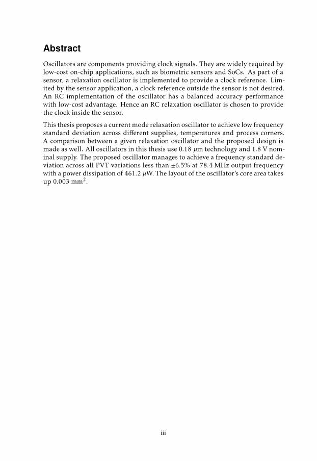
Oscillators are components providing clock signals. They are widely required bylow-cost on-chip applications, such as biometric sensors and SoCs. As part of asensor, a relaxation oscillator is implemented to provide a clock reference. Lim-ited by the sensor application, a clock reference outside the sensor is not desired.An RC implementation of the oscillator has a balanced accuracy performancewith low-cost advantage. Hence an RC relaxation oscillator is chosen to providethe clock inside the sensor.
This thesis proposes a current mode relaxation oscillator to achieve low frequencystandard deviation across different supplies, temperatures and process corners.A comparison between a given relaxation oscillator and the proposed design ismade as well. All oscillators in this thesis use 0.18 µm technology and 1.8 V nom-inal supply. The proposed oscillator manages to achieve a frequency standard de-viation across all PVT variations less than ±6.5% at 78.4 MHz output frequencywith a power dissipation of 461.2 µW. The layout of the oscillator’s core area takesup 0.003 mm2.
iii


Acknowledgments
I appreciate that Fingerprint Cards AB offers me the opportunity to work on thisthesis. The project has been challenging and meaningful.
I would like to thank Dr. Erik Säll for being my supervisor at Fingerprints. Hissuggestion always pointed out a way to solve the issue. Dr. Robert Hägglund,Anders Nordström, Dr. Christer Jansson and Dr. Prakash Harikumar helped mea lot during the project period at Fingerprints as well.
Special thanks to Dr. J Jacob Wikner and Martin Nielsen Lönn for being myexaminer and supervisor at campus. Dr. J Jacob Wikner’s guidance helped me indifferent stages of this project.
I would also like to thank my office mate Jimmy Johansson, who had workedthe whole period with me at Fingerprints. I would like to thank Carl-FredrikTengberg for teaching me the Swedish alcohol culture as well as being anotherthesis student at Fingerprints with me.
Finally I would like to thank my parents for supporting me during the past twoyears.
Linköping, June 2017Jianxing Dai
v


Contents
List of Figures x
List of Tables xii
Notation xiii
1 Introduction 11.1 Motivation and purpose . . . . . . . . . . . . . . . . . . . . . . . . 11.2 Problem statements . . . . . . . . . . . . . . . . . . . . . . . . . . . 31.3 Constraints . . . . . . . . . . . . . . . . . . . . . . . . . . . . . . . . 31.4 Methodology . . . . . . . . . . . . . . . . . . . . . . . . . . . . . . . 31.5 Scope of the dissertation . . . . . . . . . . . . . . . . . . . . . . . . 4
2 Background 52.1 Original oscillator . . . . . . . . . . . . . . . . . . . . . . . . . . . . 52.2 Simulation settings . . . . . . . . . . . . . . . . . . . . . . . . . . . 62.3 Simulation results . . . . . . . . . . . . . . . . . . . . . . . . . . . . 72.4 Specifications . . . . . . . . . . . . . . . . . . . . . . . . . . . . . . 8
3 Theory 93.1 Conventional relaxation oscillator . . . . . . . . . . . . . . . . . . . 93.2 Original design of the oscillator . . . . . . . . . . . . . . . . . . . . 10
3.2.1 Bias generation module . . . . . . . . . . . . . . . . . . . . . 123.2.2 Comparator . . . . . . . . . . . . . . . . . . . . . . . . . . . 153.2.3 Trimming control . . . . . . . . . . . . . . . . . . . . . . . . 173.2.4 SR latch . . . . . . . . . . . . . . . . . . . . . . . . . . . . . . 19
3.3 Current mode oscillator . . . . . . . . . . . . . . . . . . . . . . . . . 203.3.1 Block diagram . . . . . . . . . . . . . . . . . . . . . . . . . . 203.3.2 Circuit schematic . . . . . . . . . . . . . . . . . . . . . . . . 213.3.3 Cascode current mirror . . . . . . . . . . . . . . . . . . . . . 213.3.4 Current mode comparator . . . . . . . . . . . . . . . . . . . 25
3.4 Temperature coefficient . . . . . . . . . . . . . . . . . . . . . . . . . 273.5 Noise . . . . . . . . . . . . . . . . . . . . . . . . . . . . . . . . . . . 28
vii
viii Contents
3.6 Conclusion . . . . . . . . . . . . . . . . . . . . . . . . . . . . . . . . 28
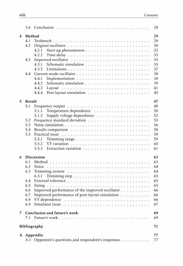
4 Method 294.1 Testbench . . . . . . . . . . . . . . . . . . . . . . . . . . . . . . . . . 294.2 Original oscillator . . . . . . . . . . . . . . . . . . . . . . . . . . . . 30
4.2.1 Start-up phenomenon . . . . . . . . . . . . . . . . . . . . . . 324.2.2 Time delay . . . . . . . . . . . . . . . . . . . . . . . . . . . . 33
4.3 Improved oscillator . . . . . . . . . . . . . . . . . . . . . . . . . . . 334.3.1 Schematic simulation . . . . . . . . . . . . . . . . . . . . . . 354.3.2 Limitations . . . . . . . . . . . . . . . . . . . . . . . . . . . . 37
4.4 Current mode oscillator . . . . . . . . . . . . . . . . . . . . . . . . . 384.4.1 Implementation . . . . . . . . . . . . . . . . . . . . . . . . . 384.4.2 Schematic simulation . . . . . . . . . . . . . . . . . . . . . . 394.4.3 Layout . . . . . . . . . . . . . . . . . . . . . . . . . . . . . . 414.4.4 Post-layout simulation . . . . . . . . . . . . . . . . . . . . . 45
5 Result 475.1 Frequency output . . . . . . . . . . . . . . . . . . . . . . . . . . . . 48
5.1.1 Temperature dependence . . . . . . . . . . . . . . . . . . . 505.1.2 Supply voltage dependence . . . . . . . . . . . . . . . . . . 52
5.2 Frequency standard deviation . . . . . . . . . . . . . . . . . . . . . 535.3 Noise simulation . . . . . . . . . . . . . . . . . . . . . . . . . . . . . 565.4 Results comparison . . . . . . . . . . . . . . . . . . . . . . . . . . . 585.5 Practical issue . . . . . . . . . . . . . . . . . . . . . . . . . . . . . . 59
5.5.1 Trimming range . . . . . . . . . . . . . . . . . . . . . . . . . 595.5.2 VT variation . . . . . . . . . . . . . . . . . . . . . . . . . . . 605.5.3 Extraction variation . . . . . . . . . . . . . . . . . . . . . . . 61
6 Discussion 636.1 Method . . . . . . . . . . . . . . . . . . . . . . . . . . . . . . . . . . 636.2 Noise . . . . . . . . . . . . . . . . . . . . . . . . . . . . . . . . . . . 646.3 Trimming system . . . . . . . . . . . . . . . . . . . . . . . . . . . . 64
6.3.1 Trimming step . . . . . . . . . . . . . . . . . . . . . . . . . . 656.4 External reference . . . . . . . . . . . . . . . . . . . . . . . . . . . . 656.5 Sizing . . . . . . . . . . . . . . . . . . . . . . . . . . . . . . . . . . . 656.6 Improved performance of the improved oscillator . . . . . . . . . . 666.7 Improved performance of post-layout simulation . . . . . . . . . . 666.8 VT dependence . . . . . . . . . . . . . . . . . . . . . . . . . . . . . 666.9 Simulator issue . . . . . . . . . . . . . . . . . . . . . . . . . . . . . . 67
7 Conclusion and future’s work 697.1 Future’s work . . . . . . . . . . . . . . . . . . . . . . . . . . . . . . . 69
Bibliography 71
A Appendix 77A.1 Opponent’s questions and respondent’s responses . . . . . . . . . . 77

Contents ix
A.2 Change track . . . . . . . . . . . . . . . . . . . . . . . . . . . . . . . 80
List of Figures
1.1 The configuration of the original oscillator. . . . . . . . . . . . . . 2
2.1 Distribution of 100-points Monte Carlo simulation at −40 C with1.98 V supply of the original oscillator. . . . . . . . . . . . . . . . . 8
3.1 Conventional relaxation oscillator schematic. . . . . . . . . . . . . 103.2 Original design of the oscillator. . . . . . . . . . . . . . . . . . . . . 113.3 Bias generation module design of the original oscillator. . . . . . . 143.4 Schmitt trigger design of the current oscillator. . . . . . . . . . . . 153.5 Comparator design of the original oscillator. . . . . . . . . . . . . . 163.6 Trimming module design of the original oscillator. . . . . . . . . . 183.7 SR latch design of the oscillators. . . . . . . . . . . . . . . . . . . . 193.8 The block diagram of the current mode oscillator. . . . . . . . . . . 203.9 The configuration of the proposed current mode oscillator. . . . . 223.10 Cascode current mirror design of the oscillator. . . . . . . . . . . . 233.11 Simplified model of the cascode current mirror design of the oscil-
lator. . . . . . . . . . . . . . . . . . . . . . . . . . . . . . . . . . . . 243.12 Current mode comparator design of the proposed oscillator. . . . . 263.13 Current comparison circuit’s timing diagram. . . . . . . . . . . . . 26
4.1 The testbench of the oscillator. . . . . . . . . . . . . . . . . . . . . . 304.2 Delayed enabling signal triggers the oscillation. . . . . . . . . . . . 314.3 Capacitor voltage in oscillation. . . . . . . . . . . . . . . . . . . . . 324.4 Comparator internal signals for upper threshold comparison in os-
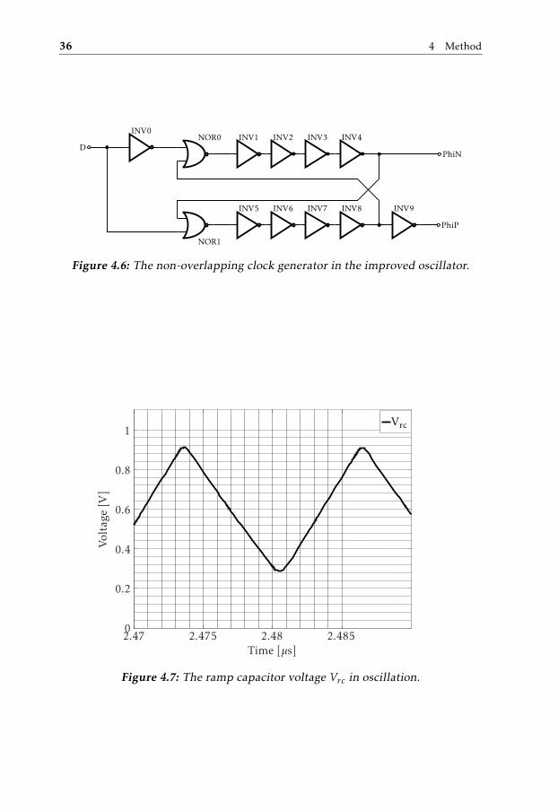
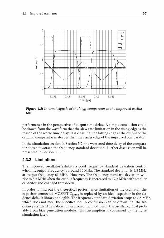
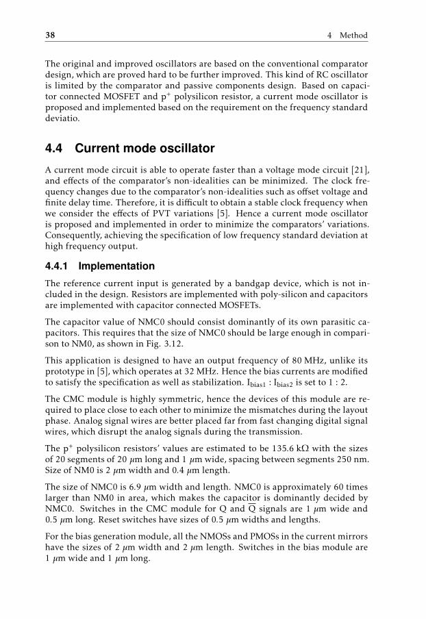
cillation. . . . . . . . . . . . . . . . . . . . . . . . . . . . . . . . . . 344.5 Improved design of the oscillator. . . . . . . . . . . . . . . . . . . . 354.6 The non-overlapping clock generator in the improved oscillator. . 364.7 The ramp capacitor voltage Vrc in oscillation. . . . . . . . . . . . . 364.8 Internal signals of the VthH comparator in the improved oscillator. 374.9 The current generated from the bias current generator at nominal
condition. . . . . . . . . . . . . . . . . . . . . . . . . . . . . . . . . . 394.10 The capacitor ramp voltages in oscillation state at nominal condi-
tion. . . . . . . . . . . . . . . . . . . . . . . . . . . . . . . . . . . . . 404.11 The output signals of the current mode comparator module in os-
cillation state at nominal condition. . . . . . . . . . . . . . . . . . . 40
x
LIST OF FIGURES xi
4.12 Top level of the proposed oscillator layout. . . . . . . . . . . . . . . 414.13 The logic module of the proposed oscillator layout. . . . . . . . . . 424.14 The bias module of the proposed oscillator layout. . . . . . . . . . 434.15 The current mode comparator module of the proposed oscillator
layout. . . . . . . . . . . . . . . . . . . . . . . . . . . . . . . . . . . 444.16 Ramp voltages of the capacitors and output signals of the current
mode comparator. . . . . . . . . . . . . . . . . . . . . . . . . . . . . 45
5.1 The original oscillator’s output waveform and frequency settlingtime. . . . . . . . . . . . . . . . . . . . . . . . . . . . . . . . . . . . . 48
5.2 The improved oscillator’s output waveform and frequency settlingtime. . . . . . . . . . . . . . . . . . . . . . . . . . . . . . . . . . . . . 48
5.3 The schematic simulation results of the proposed oscillator’s out-put waveform and frequency settling time. . . . . . . . . . . . . . . 49
5.4 The post-layout simulation results of the proposed oscillator’s out-put waveform and frequency settling time. . . . . . . . . . . . . . . 50
5.5 Temperature dependences of the implemented oscillators. . . . . . 515.6 Supply voltage dependences of the implemented oscillators. . . . . 525.7 Histogram of 100 samples at −40 C with 1.98 V supply of the orig-
inal oscillator. . . . . . . . . . . . . . . . . . . . . . . . . . . . . . . 535.8 Histogram of 100 samples at −40 C with 1.62 V supply of the im-
proved oscillator. . . . . . . . . . . . . . . . . . . . . . . . . . . . . 545.9 Histogram of 100 samples at −40 C with 1.62 V supply of the
schematic simulation of the proposed oscillator. . . . . . . . . . . . 545.10 Histogram of 100 samples at −40 C with 1.62 V supply of the post-
layout simulation of the proposed oscillator. . . . . . . . . . . . . . 555.11 The oscillators’ spectrums. . . . . . . . . . . . . . . . . . . . . . . . 565.12 The oscillators’ phase noises. . . . . . . . . . . . . . . . . . . . . . . 575.13 Trimming range of the implemented oscillators. . . . . . . . . . . . 595.14 VT variations of the implemented oscillators. . . . . . . . . . . . . 605.15 The output frequencies for different extractions of the nominal cor-
ner. . . . . . . . . . . . . . . . . . . . . . . . . . . . . . . . . . . . . 61
6.1 Histogram of 100 samples at −40 C with 1.62 V supply of the orig-inal oscillator. . . . . . . . . . . . . . . . . . . . . . . . . . . . . . . 68

List of Tables
1.1 Constraints of the design. . . . . . . . . . . . . . . . . . . . . . . . . 3
2.1 Test settings for oscillators. . . . . . . . . . . . . . . . . . . . . . . . 62.2 Simulation results of the original oscillator. . . . . . . . . . . . . . 72.3 Specifications of the proposed design. . . . . . . . . . . . . . . . . 8
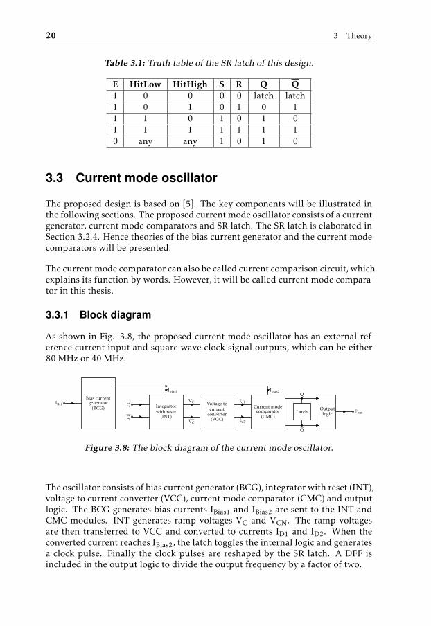
3.1 Truth table of the SR latch of this design. . . . . . . . . . . . . . . . 20
5.1 Simulation results comparison between the original oscillator andthe improved oscillator. . . . . . . . . . . . . . . . . . . . . . . . . . 49
5.2 Simulation results comparison between the schematic and the lay-out of the proposed oscillator. . . . . . . . . . . . . . . . . . . . . . 50
5.3 The comparison between different implementations’ Monte Carlosimulation results. . . . . . . . . . . . . . . . . . . . . . . . . . . . . 55
5.4 The noise simulation results’ comparison table. . . . . . . . . . . . 575.5 Results comparison. . . . . . . . . . . . . . . . . . . . . . . . . . . . 585.6 VT variations caparison. . . . . . . . . . . . . . . . . . . . . . . . . 61
A.1 Document history. . . . . . . . . . . . . . . . . . . . . . . . . . . . . 80
xii
Notation
Abbreviations
Abbreviation Description
BCG Bias Current GeneratorCMC Current Mode Comparatorcmos Complementary Metal Oxide SemiconductorCS Common SourceDFF D-Flip FlopFoM Figure of MeritINT IntegratorLSB Least Significant BitLUT Look-Up TableMC Monte Carloopamp Operational AmplifierPVT Process, Voltage and TemperaturePSS Periodic Steady StateRGC Regulated CascodeTCR Temperature Coefficient of ResistanceVCC Voltage Current ConverterVT Voltage and Temperature
xiii

1Introduction
In electronics a relaxation oscillator is a nonlinear electronic oscillator circuitthat produces a non-sinusoidal repetitive output signal, such as a triangle waveor square wave [1]. The circuit consists of a feedback loop containing a switchingdevice such as a transistor, comparator, op amp, or a negative resistance devicelike a tunnel diode, that repetitively charges a capacitor or inductor through aresistance until it reaches a threshold level, then discharges it again [2].
The period of the oscillator depends on the time constant of the capacitor or in-ductor circuit. [3] The active device switches abruptly between charging and dis-charging modes, and thus produces a discontinuously changing repetitive wave-form [2]. This contrasts with the other type of electronic oscillator, the harmonicor linear oscillator, which uses an amplifier with feedback to excite resonant os-cillations in a resonator, producing a sine wave [4].
1.1 Motivation and purpose
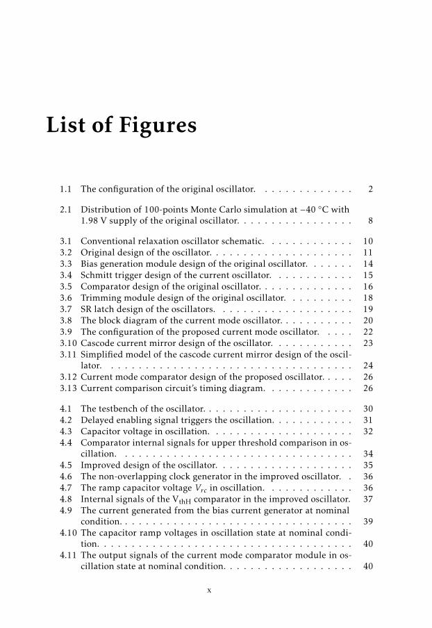
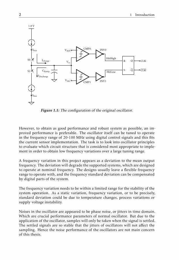
There was a given relaxation oscillator using RC architecture to generate squarewave clock signal. This oscillator operates with 1.8 V supply voltage and is imple-mented with 0.18 µm technology. The given oscillator can output a square waveclock of 86 MHz with nominal process corner, 1.8 V supply and 25 C tempera-ture. The given oscillator is shown in Fig. 1.1 and will be further described inChapter 2 and 3.
1
2 1 Introduction
Ibias
S1
S0
Ibias
1.8 V
CRamp
−
+
−
+
CMP0
CMP1
Vrc
VthH
VthL
INV0
INV1
R
S
Q
Q
CLK
CLK
HitHigh
HitLow
ICharge
IDischarge
Figure 1.1: The configuration of the original oscillator.
However, to obtain as good performance and robust system as possible, an im-proved performance is preferable. The oscillator itself can be tuned to operatein the frequency range of 20-100 MHz using digital control signals and this fitsthe current sensor implementation. The task is to look into oscillator principlesto evaluate which circuit structure that is considered most appropriate to imple-ment in order to obtain low frequency variations over a large tuning range.
A frequency variation in this project appears as a deviation to the mean outputfrequency. The deviation will degrade the supported systems, which are designedto operate at nominal frequency. The designs usually leave a flexible frequencyrange to operate with, and the frequency standard deviation can be compensatedby digital parts of the system.
The frequency variation needs to be within a limited range for the stability of thesystem operation. As a static variation, frequency variation, or to be precisely,standard deviation could be due to temperature changes, process variations orsupply voltage instability.
Noises in the oscillator are appeared to be phase noise, or jitters in time domain.Which are crucial performance parameters of normal oscillator. But due to theapplication of the oscillator, samples will only be taken when the signal is settled.The settled signals are so stable that the jitters of oscillators will not affect thesampling. Hence the noise performance of the oscillators are not main concernof this thesis.

1.2 Problem statements 3
1.2 Problem statements
This thesis will cover the following questions.
• What other kinds of architectures can be used to achieve a relaxation oscil-lator?
• Which component of the design is the main reason for output frequencyvariation across different process, temperature and supply voltage corners?
• Which devices of the components are more exposed to process, temperatureand supply changes?
The questions will be discussed and answered in the following chapters.
1.3 Constraints
This project is aiming to improve the existing design of the relaxation oscillator.Hence the design is limited with process technology, supply voltage, tempera-ture range and output signal type, as shown in Tab. 1.1. The design will beutilized in schematic level and a layout based on the schematic design will be per-formed. Hence the evaluation will be based on the simulations, which consists ofschematic simulation and post-layout simulation.
Table 1.1: Constraints of the design.
Supply voltage (V) 1.62 - 1.98Temperature (C) −40 - 85Process technology (nm) 180Output signal form Square waveDesign form Schematic & LayoutResults sources Simulations
1.4 Methodology
The methodology includes preliminary literature survey to decide appropriatecircuit design and state-of-the-art performance. Based on system specifications,the design parameters of the circuit blocks are derived. The implementationsof different modules are carried out subsequently. The design is implementedby combining circuit techniques from different publications as well as adoptingmodifications of the original design. Simulations are performed with differentprocess corners, supply voltages and temperatures.

4 1 Introduction
1.5 Scope of the dissertation
This thesis is organized as the following structure:
• Chapter 2 discusses the design specifications for the oscillator. The originaloscillator’s simulation results are listed as well.
• Chapter 3 presents the working principles of different components insidethe oscillators. This chapter is based on various publications and originaloscillator’s circuit design.
• Chapter 4 presents the implementations of an improved version of the orig-inal oscillator and a new proposal of a relaxation oscillator.
• Chapter 5 presents results of the two implemented oscillators and a com-parison between different relaxation oscillators.
• Chapter 6 presents conclusions and discussions of the results. A widerperspective of this work is also concluded.
An appendix of the opponent’s comments and author’s replies is included at thefinal part of the report.
2Background
As mentioned in Section 1.1, the thesis is aiming to improve the existing design orpropose a new implementation. Thus this chapter focuses on the original designand the specifications. The simulation results of the original oscillator based onschematic design are listed in this chapter. The worst corner of the frequencystandard deviation is shown in histograms.
The distribution of the Monte Carlo simulation results are evaluated with the3σ rule, which is used to measure samples’ deviations to the mean value of testresults. To include all simulation results into 3σ range, a standard deviationneeds to be adjusted. Hence a wide spread distribution of the simulation resultswill result in a large standard deviation of the output frequency, which needs tobe avoided.
The proposed design should be able to easily integrate into the existing system.This requires some key features to be maintained, such as the trimming signalcombined with the control code.
2.1 Original oscillator
The original oscillator has the configuration as shown in Fig. 1.1. It consistsof two current sources charging and discharging the ramp capacitor CRamp, twocomparators connected with inverters and an SR latch as the output logic.
It should be noticed that the two bias current mirrors are controlled by trimmingcodes outside the oscillator. The trimming code changes the amount of the charg-ing and discharging current, consequently adjusts the output frequency.
The trimming code ranges from −8 to 7 in decimal, but realized in two’s com-
5
6 2 Background
plement in the oscillator. In the original oscillator, the trimming code is a fivebits two’s complement code. The five bits control code requires five branchesof current mirrors. They are parallel connected MOSFETs and the numbers ofMOSFETs in each branch are determined by 2n. A detailed description of thetrimming control module is included in Section 3.2.3.
2.2 Simulation settings
The original oscillator and the proposed oscillator will be evaluated under tran-sient simulations and Monte Carlo simulations. Nominal cases transient simula-tions provide nominal output frequencies, settling time, duty cycles and currentconsumptions of the tested oscillators. The Monte Carlo simulations provide theoutput frequency standard deviations of the oscillators. The supply voltages areprovided by ideal DC voltage source.
Simulation settings are shown in Tab. 2.1 below. It should be noted that trim-ming codes differ from each other for different purposes. That is the reason for"depends" in the table. When a tuning range of an oscillator is to be tested, thetrimming code will be swept from −8 to 7. When an output frequency is to betested, the trimming code will be fixed to 0.
The process corner 0 means typical corner. Different combinations of NMOSsand PMOSs corners are named after 1 to 12. The process corner 100 is for therecognition by the MC models. Hence the process corner 100 can be translatedas "Monte Carlo model process corner setting".
Table 2.1: Test settings for oscillators.
Simulation Transient Monte CarloSupply (V) 1.8 1.62, 1.98
Temperature (C) 25 -40, 25, 85Process Corner 0 100Trimming Code Depends 0
Apart from the VT settings and process corner settings, Monte Carlo simulationshave more options than transient simulations. The variation setting is set to "all",which means process variations and mismatches are both simulated during theMC simulations. The sampling method is set to "random". The process variationis covered by the MC simulation model, hence VT variations are sufficient for MCcorner settings.
It should be noticed that the process corner setting for the MC simulations are notenough to cover all process corner variations. Due to the limitations on resources,simulations for all process variations are not feasible. Hence a simplified MC pro-cess corner setting is used to estimate the oscillator’s performances. VT variationswith MC simulations can not give identical results to the PVT simulations.
2.3 Simulation results 7
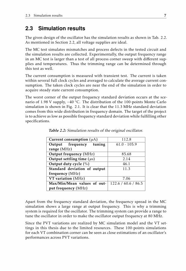
2.3 Simulation results
The given design of the oscillator has the simulation results as shown in Tab. 2.2.As mentioned in Section 2.2, all voltage supplies are ideal.
The MC test simulates mismatches and process defects in the tested circuit andthe simulation results are collected. Experimentally, the output frequency rangein an MC test is larger than a test of all process corner sweep with different sup-plies and temperatures. Thus the trimming range can be determined throughthis test as well.
The current consumption is measured with transient test. The current is takenwithin several full clock cycles and averaged to calculate the average current con-sumption. The taken clock cycles are near the end of the simulation in order toacquire steady state current consumption.
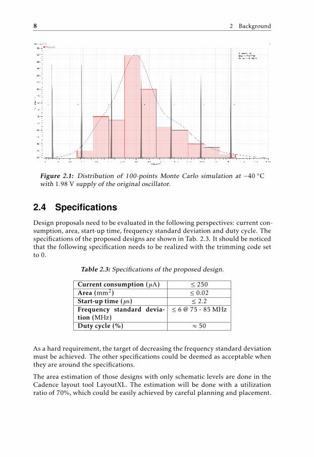
The worst corner of the output frequency standard deviation occurs at the sce-nario of 1.98 V supply, −40 C. The distribution of the 100-points Monte Carlosimulation is shown in Fig. 2.1. It is clear that the 11.3 MHz standard deviationcomes from this wide distribution in frequency domain. The target of the projectis to achieve as low as possible frequency standard deviation while fulfilling otherspecifications.
Table 2.2: Simulation results of the original oscillator.
Current consumption (µA) 112.8Output frequency tuningrange (MHz)
61.0 - 105.9
Output frequency (MHz) 85.68Output settling time (µs) 2.14Output duty cycle (%) 46.1Standard deviation of outputfrequency (MHz)
11.3
VT variation (MHz) 7.06Max/Min/Mean values of out-put frequency (MHz)
122.6 / 60.6 / 86.5
Apart from the frequency standard deviation, the frequency spread in the MCsimulation shows a large range at output frequency. This is why a trimmingsystem is required for the oscillator. The trimming system can provide a range totune the oscillator in order to make the oscillator output frequency at 80 MHz.
Since the PVT variations are realized by MC simulation model and the VT set-tings in this thesis due to the limited resources. These 100-points simulationsfor each VT combination corner can be seen as close estimations of an oscillator’sperformances across PVT variations.
8 2 Background
Figure 2.1: Distribution of 100-points Monte Carlo simulation at −40 Cwith 1.98 V supply of the original oscillator.
2.4 Specifications
Design proposals need to be evaluated in the following perspectives: current con-sumption, area, start-up time, frequency standard deviation and duty cycle. Thespecifications of the proposed designs are shown in Tab. 2.3. It should be noticedthat the following specification needs to be realized with the trimming code setto 0.
Table 2.3: Specifications of the proposed design.
Current consumption (µA) ≤ 250Area (mm2) ≤ 0.02Start-up time (µs) ≤ 2.2Frequency standard devia-tion (MHz)
≤ 6 @ 75 - 85 MHz
Duty cycle (%) ≈ 50
As a hard requirement, the target of decreasing the frequency standard deviationmust be achieved. The other specifications could be deemed as acceptable whenthey are around the specifications.
The area estimation of those designs with only schematic levels are done in theCadence layout tool LayoutXL. The estimation will be done with a utilizationratio of 70%, which could be easily achieved by careful planning and placement.
3Theory
This chapter will focus on the relaxation oscillator’s working principles, whichinvolve both the oscillator and the sub-modules.
A conventional relaxation oscillator will be described first. Then different com-ponents of the original oscillator design will be elaborated. At last, the key com-ponents of the proposed design will be showed.
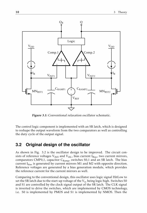
The original oscillator was designed based on the conventional voltage moderelaxation oscillator. Unlike common relaxation oscillators, the original designachieved an output frequency as high as 85 MHz. The high frequency output in-evitably leads to high frequency standard deviation. Thus a current mode relax-ation oscillator is proposed in this work, aiming to reduce the frequency standarddeviation and keep the output frequency at a range of 75 - 85 MHz.
3.1 Conventional relaxation oscillator
As shown in Fig. 3.1 is a conventional voltage mode relaxation oscillator. The cir-cuit consists of bias currents IBs, a reference voltage VREF, comparators Comp.1,2capacitors CRAMP1,2 reset switches MNRST1,2, and a control logic circuit. When Qand QB are high and low, MNRST1 and MNRST2 are off and on, respectively. TheCRAMP1 accepts IB and generates ramp voltage of VINT1. The Comp.1 comparesVINT1 with VREF. When the VINT1 reaches VREF, the Comp.1 detects it and Q andQB toggle low and high, respectively. By repeating above operation alternatelyfor CRAMP1 and CRAMP2, the circuit generates a clock pulse [5].
9
10 3 Theory
MNRST1CRAMP1 +
−
VREF
CRAMP2MNRST2
−+
Comp.1
− +
Comp.2
IB IB
VDD VDD
Logic
QB Q
VINT1 VINT2
Figure 3.1: Conventional relaxation oscillator schematic.
The control logic component is implemented with an SR latch, which is designedto reshape the output waveform from the two comparators as well as controllingthe duty cycle of the output signal.
3.2 Original design of the oscillator
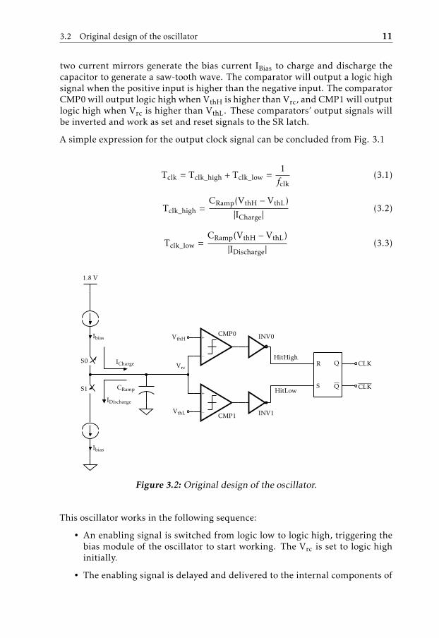
As shown in Fig. 3.2 is the oscillator design to be improved. The circuit con-sists of reference voltages VthH and VthL, bias current IBias, two current mirrors,comparators CMP0,1, capacitor CRamp, switches S0,1 and an SR latch. The biascurrent Ibias is generated by current mirrors M1 and M2 with opposite direction.Reference voltages are generated by a bias generation module, which providesthe reference current for the current mirrors as well.
Comparing to the conventional design, this oscillator uses logic signal HitLow toset the SR latch due to the start-up voltage of the Vrc being logic high. Switches S0and S1 are controlled by the clock signal output of the SR latch. The CLK signalis inverted to drive the switches, which are implemented by CMOS technology,i.e. S0 is implemented by PMOS and S1 is implemented by NMOS. Then the
3.2 Original design of the oscillator 11
two current mirrors generate the bias current IBias to charge and discharge thecapacitor to generate a saw-tooth wave. The comparator will output a logic highsignal when the positive input is higher than the negative input. The comparatorCMP0 will output logic high when VthH is higher than Vrc, and CMP1 will outputlogic high when Vrc is higher than VthL. These comparators’ output signals willbe inverted and work as set and reset signals to the SR latch.
A simple expression for the output clock signal can be concluded from Fig. 3.1
Tclk = Tclk_high + Tclk_low =1fclk
(3.1)
Tclk_high =CRamp(VthH − VthL)
|ICharge|(3.2)
Tclk_low =CRamp(VthH − VthL)
|IDischarge|(3.3)
Ibias
S1
S0
Ibias
1.8 V
CRamp
−
+
−
+
CMP0
CMP1
Vrc
VthH
VthL
INV0
INV1
R
S
Q
Q
CLK
CLK
HitHigh
HitLow
ICharge
IDischarge
Figure 3.2: Original design of the oscillator.
This oscillator works in the following sequence:
• An enabling signal is switched from logic low to logic high, triggering thebias module of the oscillator to start working. The Vrc is set to logic highinitially.
• The enabling signal is delayed and delivered to the internal components of
12 3 Theory
the oscillator.
• The CRamp begins to discharge after the trimming control module is acti-vated.
• When the Vrc touches the low threshold voltage VthL, the CMP1 outputsignal toggles and HitLow changes to logic high, which set the SR latchoutput Q to logic high.
• The switch S1 turns off and S0 turns on. The Camp begins to charge afterthe CLK signal toggling to logic high.
• When the Vrc touches the high threshold voltage VthH, the CMP0 outputsignal toggles and HitHigh changes to logic high, which reset the SR latchoutput Q to logic low.
Then the oscillator keeps on oscillating until the enabling signal toggles to logiclow. Which shuts down the oscillator.
The generated clock is used to take samples in the rest part of the circuit. Eachsample will be taken at steady state, hence the jitter is not of concern in thisapplication. Samples will be taken at their settled states, while the clock willbe used at lower frequency to take the samples. Combining these two featurestogether, clock jitters, or phase noises, of an oscillator is not one of the mainpursuits of an oscillator design.
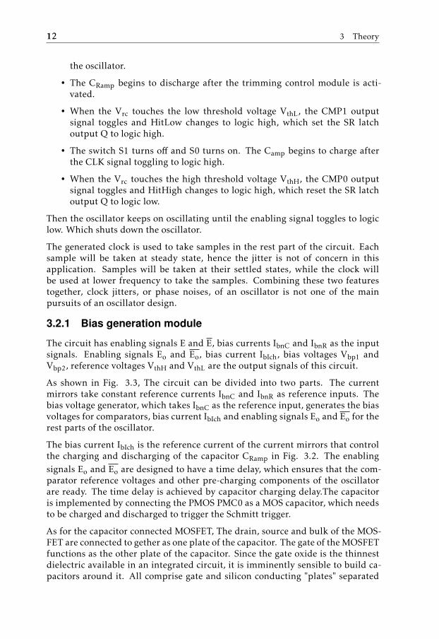
3.2.1 Bias generation module
The circuit has enabling signals E and E, bias currents IbnC and IbnR as the inputsignals. Enabling signals Eo and Eo, bias current IbIch, bias voltages Vbp1 andVbp2, reference voltages VthH and VthL are the output signals of this circuit.
As shown in Fig. 3.3, The circuit can be divided into two parts. The currentmirrors take constant reference currents IbnC and IbnR as reference inputs. Thebias voltage generator, which takes IbnC as the reference input, generates the biasvoltages for comparators, bias current IbIch and enabling signals Eo and Eo for therest parts of the oscillator.
The bias current IbIch is the reference current of the current mirrors that controlthe charging and discharging of the capacitor CRamp in Fig. 3.2. The enablingsignals Eo and Eo are designed to have a time delay, which ensures that the com-parator reference voltages and other pre-charging components of the oscillatorare ready. The time delay is achieved by capacitor charging delay.The capacitoris implemented by connecting the PMOS PMC0 as a MOS capacitor, which needsto be charged and discharged to trigger the Schmitt trigger.
As for the capacitor connected MOSFET, The drain, source and bulk of the MOS-FET are connected to gether as one plate of the capacitor. The gate of the MOSFETfunctions as the other plate of the capacitor. Since the gate oxide is the thinnestdielectric available in an integrated circuit, it is imminently sensible to build ca-pacitors around it. All comprise gate and silicon conducting "plates" separated
3.2 Original design of the oscillator 13
by the gate oxide as dielectric. All are nonlinear capacitors, whose value dependson the voltage across it [6].
The threshold voltage generator, which takes IbnR as reference input, generatesthe reference voltages for comparators. The circuit uses a resistor R2 to compen-sate the temperature variation in the voltage divider. Similar resistor values of R2and R1 are taken. As shown in Fig. 3.3, threshold voltages are set by series con-nected resistors R0 and R1. The two capacitors NMC0 and NMC1 are decouplingcapacitors to stabilize the output threshold voltages.
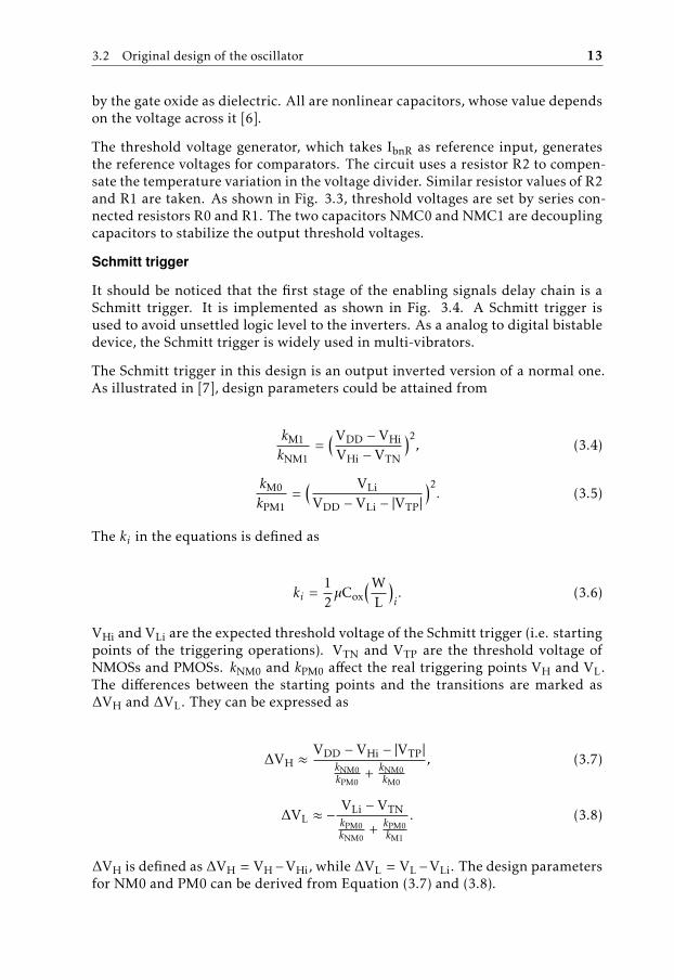
Schmitt trigger
It should be noticed that the first stage of the enabling signals delay chain is aSchmitt trigger. It is implemented as shown in Fig. 3.4. A Schmitt trigger isused to avoid unsettled logic level to the inverters. As a analog to digital bistabledevice, the Schmitt trigger is widely used in multi-vibrators.
The Schmitt trigger in this design is an output inverted version of a normal one.As illustrated in [7], design parameters could be attained from
kM1
kNM1=
(VDD − VHi
VHi − VTN
)2, (3.4)
kM0
kPM1=
( VLi
VDD − VLi − |VTP|)2. (3.5)
The ki in the equations is defined as
ki =12µCox
(WL
)i. (3.6)
VHi and VLi are the expected threshold voltage of the Schmitt trigger (i.e. startingpoints of the triggering operations). VTN and VTP are the threshold voltage ofNMOSs and PMOSs. kNM0 and kPM0 affect the real triggering points VH and VL.The differences between the starting points and the transitions are marked as∆VH and ∆VL. They can be expressed as
∆VH ≈VDD − VHi − |VTP|
kNM0kPM0
+ kNM0kM0
, (3.7)
∆VL ≈ −VLi − VTNkPM0kNM0
+ kPM0kM1
. (3.8)
∆VH is defined as ∆VH = VH−VHi, while ∆VL = VL−VLi. The design parametersfor NM0 and PM0 can be derived from Equation (3.7) and (3.8).
14 3 Theory
NM
0N
M1
NM
e0
NM
e1
IbnC
EE
PM0
PM1
PMe0
PMe1
NM
2
Vbp
1V
bp2
NM
3N
M4
NM
5
PMe2
IbIch
PMC
0
Schmitt
INV
0
INV
1
Eo
Eo
IbnR
NM
6
NM
e2
NM
e3
NM
7
PM2
PMe3
R2
EE
E
PM3
NM
C1
NM
C0
R0
R1
1.8V
VthH
VthL
Bias
Voltage
Generator
Threshold
Voltage
Generator
Figure
3.3:Bias
generationm
odule
design
ofthe
originaloscillator.
3.2 Original design of the oscillator 15
M1
NM0
PM0
M0
NM1
PM1
A Y
1.8 V
1.8 V
Figure 3.4: Schmitt trigger design of the current oscillator.
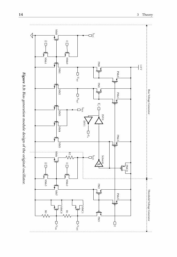
3.2.2 Comparator
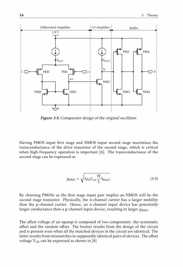
The comparator in this oscillator is a component that compares two signals atthe input ports and generates a logic signals accordingly at the output port. Asshown in Fig. 3.5, the comparator consists of a differential amplifier, a commonsource amplifier and a buffer. The buffer turns the two-stage amplifier outputinto a logic signal driving the following inverters and the SR latch.
It should be noticed that the comparator aims to output a logic signal. Thusthe gain of the first stage of the amplifier needs to be reasonable to avoid wrongoperating region for the second stage NMOS. If the voltage difference at the firststage of the amplifier is not amplified larger than the threshold voltage of NM2,the second stage of the amplifier will work in sub-threshold region, which needsto be avoided in the comparator. However, a large gain in the first stage requiresa large input pair, which introduces larger parasitic into the connecting node ofCRamp consequently, resulting in worse speed performance. The slew rate of theamplifier is critical for the comparator design in this oscillator.
16 3 Theory
NM0 NM1
PM0 PM1
Ibias1
NM2
Ibias2
NM3
PM3
NM4
PM4
1.8 V
i- i+ Y
a+
b-
Differential Amplifier CS Amplifier Buffer
Figure 3.5: Comparator design of the original oscillator.
Having PMOS input first stage and NMOS input second stage maximizes thetransconductance of the drive transistor of the second stage, which is criticalwhen high-frequency operation is important [6]. The transconductance of thesecond stage can be expressed as
gNM2 =
√2µnCox
WL
Ibias2. (3.9)
By choosing PMOSs as the first stage input pair implies an NMOS will be thesecond stage transistor. Physically, the n-channel carrier has a larger mobilitythan the p-channel carrier. Hence, an n-channel input device has potentiallylarger conductance than a p-channel input device, resulting in larger gNM2.
The offset voltage of an opamp is composed of two components: the systematicoffset and the random offset. The former results from the design of the circuitand is present even when all the matched devices in the circuit are identical. Thelatter results from mismatches in supposedly identical pairs of devices. The offsetvoltage VOS can be expressed as shown in [8]
3.2 Original design of the oscillator 17
VOS ≈ ∆Vt(PM0,PM1) + ∆Vt(NM0,NM1)gNM0
gPM0
+Veff(PM0,PM1)
2
[∆(WL
)NM0,NM1(
WL
)NM0,NM1
−∆(
WL
)PM0,P M1(
WL
)PM0,P M1
]. (3.10)
In Equation (3.10), ∆Vt is the threshold mismatch, while ∆Veff is the effectivevoltage driving the gate. For low noise and random input offset voltage, NM0and NM1 should have small transconductances comparing to the input PMOSpair and longer channel lengths than the PMOSs [8].
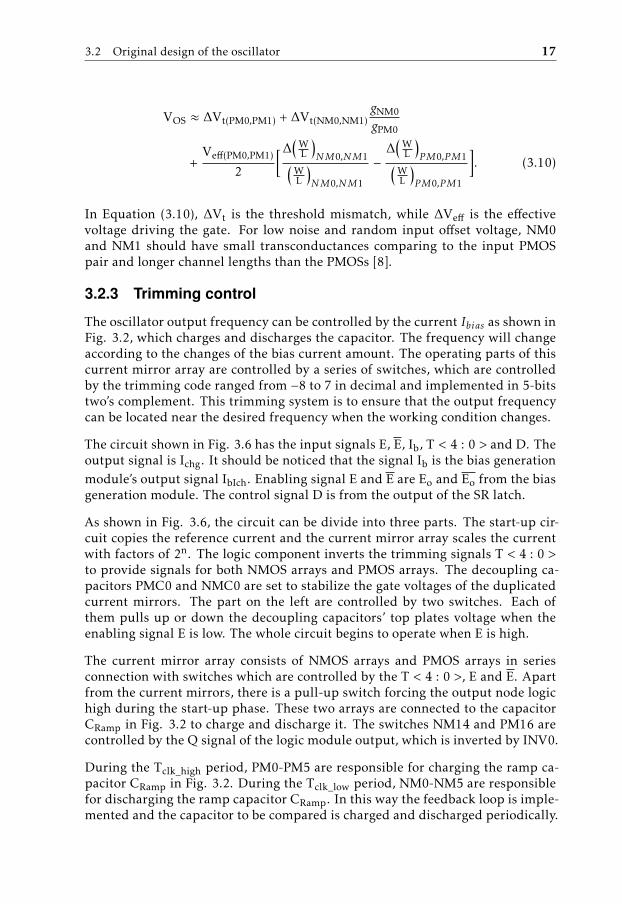
3.2.3 Trimming control
The oscillator output frequency can be controlled by the current Ibias as shown inFig. 3.2, which charges and discharges the capacitor. The frequency will changeaccording to the changes of the bias current amount. The operating parts of thiscurrent mirror array are controlled by a series of switches, which are controlledby the trimming code ranged from −8 to 7 in decimal and implemented in 5-bitstwo’s complement. This trimming system is to ensure that the output frequencycan be located near the desired frequency when the working condition changes.
The circuit shown in Fig. 3.6 has the input signals E, E, Ib, T < 4 : 0 > and D. Theoutput signal is Ichg. It should be noticed that the signal Ib is the bias generationmodule’s output signal IbIch. Enabling signal E and E are Eo and Eo from the biasgeneration module. The control signal D is from the output of the SR latch.
As shown in Fig. 3.6, the circuit can be divide into three parts. The start-up cir-cuit copies the reference current and the current mirror array scales the currentwith factors of 2n. The logic component inverts the trimming signals T < 4 : 0 >to provide signals for both NMOS arrays and PMOS arrays. The decoupling ca-pacitors PMC0 and NMC0 are set to stabilize the gate voltages of the duplicatedcurrent mirrors. The part on the left are controlled by two switches. Each ofthem pulls up or down the decoupling capacitors’ top plates voltage when theenabling signal E is low. The whole circuit begins to operate when E is high.
The current mirror array consists of NMOS arrays and PMOS arrays in seriesconnection with switches which are controlled by the T < 4 : 0 >, E and E. Apartfrom the current mirrors, there is a pull-up switch forcing the output node logichigh during the start-up phase. These two arrays are connected to the capacitorCRamp in Fig. 3.2 to charge and discharge it. The switches NM14 and PM16 arecontrolled by the Q signal of the logic module output, which is inverted by INV0.
During the Tclk_high period, PM0-PM5 are responsible for charging the ramp ca-pacitor CRamp in Fig. 3.2. During the Tclk_low period, NM0-NM5 are responsiblefor discharging the ramp capacitor CRamp. In this way the feedback loop is imple-mented and the capacitor to be compared is charged and discharged periodically.
18 3 Theory
1.8V
PMe0
PM7<
1:0>
PM15<
1:0>
PM6<
1:0>
PM14<
1:0>
PMC
0
PM5<
9:0>
PM13<
9:0>
PM4<
15:0>
PM12<
15:0>
PM3<
7:0>
PM11<
7:0>
PM2<
3:0>
PM10<
3:0>
PM1<
1:0>
PM9<
1:0>
PM0
PM8
PMe1
EET
2<
4>
T2<
3>
T2<
2>
T2<
1>
T2<
0>
E
Ib
INV
2<4:0>IN
V1<
4:0>
T<
4:0>
T2<
4:0>
T2<
4:0>
PM16
NM
14
INV
0
DIchg
NM
e0
NM
C0
NM
6<1:0>
NM
13<1:0>
NM
5<9:0>
NM
12<9:0>
NM
4<15:0>
NM
1<15:0>
NM
3<7:0>
NM
10<7:0>
NM
2<3:0>
NM
9<3:0>
NM
1<1:0>
NM
8<1:0>
NM
0
NM
7
E ET
2<
4>
T2<
3>
T2<
2>
T2<
1>
T2<
0>
Start-up
Circu
itC
urrent
Mirror
Array
Logic
Figure
3.6:Trimm
ingm
odule
design
ofthe
originaloscillator.
3.2 Original design of the oscillator 19
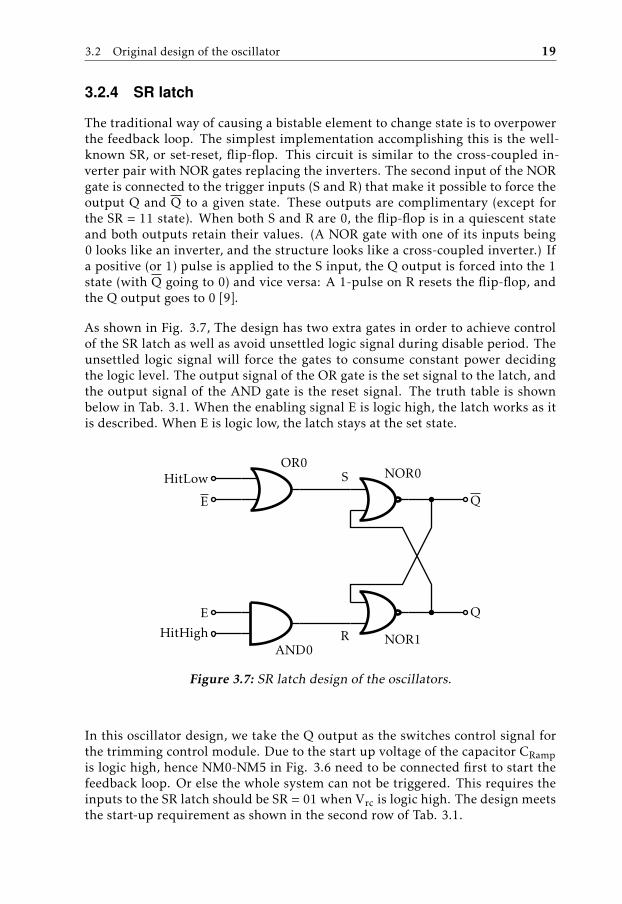
3.2.4 SR latch
The traditional way of causing a bistable element to change state is to overpowerthe feedback loop. The simplest implementation accomplishing this is the well-known SR, or set-reset, flip-flop. This circuit is similar to the cross-coupled in-verter pair with NOR gates replacing the inverters. The second input of the NORgate is connected to the trigger inputs (S and R) that make it possible to force theoutput Q and Q to a given state. These outputs are complimentary (except forthe SR = 11 state). When both S and R are 0, the flip-flop is in a quiescent stateand both outputs retain their values. (A NOR gate with one of its inputs being0 looks like an inverter, and the structure looks like a cross-coupled inverter.) Ifa positive (or 1) pulse is applied to the S input, the Q output is forced into the 1state (with Q going to 0) and vice versa: A 1-pulse on R resets the flip-flop, andthe Q output goes to 0 [9].
As shown in Fig. 3.7, The design has two extra gates in order to achieve controlof the SR latch as well as avoid unsettled logic signal during disable period. Theunsettled logic signal will force the gates to consume constant power decidingthe logic level. The output signal of the OR gate is the set signal to the latch, andthe output signal of the AND gate is the reset signal. The truth table is shownbelow in Tab. 3.1. When the enabling signal E is logic high, the latch works as itis described. When E is logic low, the latch stays at the set state.
NOR0
NOR1AND0
OR0HitLow
E
E
HitHigh
Q
Q
S
R
Figure 3.7: SR latch design of the oscillators.
In this oscillator design, we take the Q output as the switches control signal forthe trimming control module. Due to the start up voltage of the capacitor CRampis logic high, hence NM0-NM5 in Fig. 3.6 need to be connected first to start thefeedback loop. Or else the whole system can not be triggered. This requires theinputs to the SR latch should be SR = 01 when Vrc is logic high. The design meetsthe start-up requirement as shown in the second row of Tab. 3.1.
20 3 Theory
Table 3.1: Truth table of the SR latch of this design.
E HitLow HitHigh S R Q Q1 0 0 0 0 latch latch1 0 1 0 1 0 11 1 0 1 0 1 01 1 1 1 1 1 10 any any 1 0 1 0
3.3 Current mode oscillator
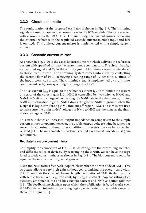
The proposed design is based on [5]. The key components will be illustrated inthe following sections. The proposed current mode oscillator consists of a currentgenerator, current mode comparators and SR latch. The SR latch is elaborated inSection 3.2.4. Hence theories of the bias current generator and the current modecomparators will be presented.
The current mode comparator can also be called current comparison circuit, whichexplains its function by words. However, it will be called current mode compara-tor in this thesis.
3.3.1 Block diagram
As shown in Fig. 3.8, the proposed current mode oscillator has an external ref-erence current input and square wave clock signal outputs, which can be either80 MHz or 40 MHz.
Bias currentgenerator
(BCG) Integratorwith reset
(INT)
Voltage tocurrent
converter(VCC)
Current modecomparator
(CMC)
OutputlogicLatch
IRef
Ibias1 Ibias2
Q
Q
VC
VC
Id2
Id1
Q
Q
Fout
Figure 3.8: The block diagram of the current mode oscillator.
The oscillator consists of bias current generator (BCG), integrator with reset (INT),voltage to current converter (VCC), current mode comparator (CMC) and outputlogic. The BCG generates bias currents IBias1 and IBias2 are sent to the INT andCMC modules. INT generates ramp voltages VC and VCN. The ramp voltagesare then transferred to VCC and converted to currents ID1 and ID2. When theconverted current reaches IBias2, the latch toggles the internal logic and generatesa clock pulse. Finally the clock pulses are reshaped by the SR latch. A DFF isincluded in the output logic to divide the output frequency by a factor of two.
3.3 Current mode oscillator 21
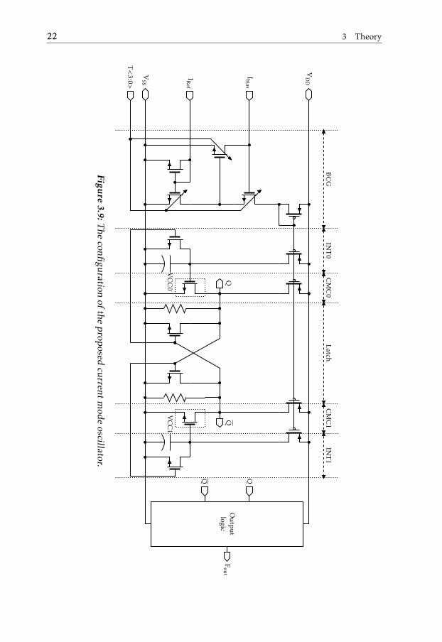
3.3.2 Circuit schematic
The configuration of the proposed oscillator is shown in Fig. 3.9. The trimmingsignals are used to control the current flow in the BCG module. They are markedwith arrows cross the MOSFETs. For simplicity, the current mirror deliveringthe external reference to the regulated cascode current mirror’s input and biasis omitted. This omitted current mirror is implemented with a simple currentmirror.
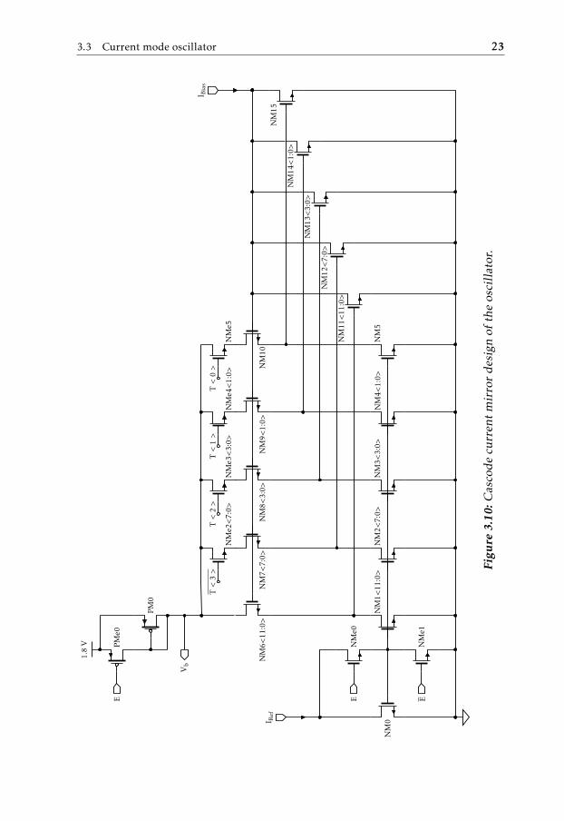
3.3.3 Cascode current mirror
As shown in Fig. 3.10 is the cascode current mirror which delivers the referencecurrent with specified ratio to the current mode comparators. The circuit has IRefas the input signal and Vb as the output signal. A trimming system is introducedto this current mirror. The trimming system comes into effect by controllingthe current flow of PM0, achieving a tuning range of 12 times to 27 times ofthe input reference current. The trimming signal is implemented by 4-bits two’scomplement code, corresponding to a range of −8 to 7.
The bias current IBias is equal to the reference current IRef to minimize the system-atic error of the current gain [10]. NM0 is controlled by two switches NMe0 andNMe1. NMe0 is in charge of connecting the NM0 gate to the drain node, forcingNM0 into saturation region. NMe1 drags the gate of NM0 to ground when theE signal is logic low, forcing NM0 into cut-off region. NM11 to NM15 are usedto make sure the drain nodes’ voltages of NM1 to NM5 are the same as the drainnode’s voltage of NM0.
This circuit shows an increased output impedance in comparison to the simplecurrent mirror or opamp, however, the usable output-voltage swing becomes nar-rower. By choosing optimum bias condition, this restriction can be somewhatrelaxed [11]. The implemented structure is called a regulated cascode (RGC) cur-rent mirror.
Regulated cascode current mirror
To simplify the connection of Fig. 3.10, we can ignore the controlling switchesand different ratios of devices. By rearranging the circuit, we can have the regu-lated cascode current mirror as shown in Fig. 3.11. The bias current is set to beequal to the input current IIn avoid gain error.
NM2 and NM3 form a feedback loop which stabilize the drain node of NM1. Thisstructure allows a very high gain without compromising the overall bandwidth[12]. To mitigate the effect of channel length modulation of NM1, its drain-sourcevoltage has been fixed (Vds1 constant) by using a feedback loop consisting of anauxiliary amplifier (NM2 and bias current source) and NM3 as source follower[13]. The feedback mechanism upon which the stabilization is based works evenif NM3 is driven into ohmic operating region, which extends the usable range forthe output signal [11].
22 3 Theory
Ou
tpu
tlogic
T<
3:0>
IRef
Ibias
Fou
t
VSS
VD
D
BC
GIN
T0
CM
C0
Latch
CM
C1
INT
1
VC
C0
VC
C1
Figure
3.9:The
configu
rationof
thep
roposed
current
mod
eoscillator.
3.3 Current mode oscillator 23
NM
0
NM
e0
NM
e1
NM
1<11
:0>
NM
2<7:
0>N
M3<
3:0>
NM
4<1:
0>N
M5
NM
11<
11:0
>
NM
12<
7:0>
NM
13<
3:0>
NM
14<
1:0>
NM
15N
M6<
11:0
>N
M7<
7:0>
NM
8<3:
0>N
M9<
1:0>
NM
10
NM
e2<
7:0>
NM
e3<
3:0>
NM
e4<
1:0>
NM
e5
PM0
PMe0
1.8
V
I Ref
E E
I Bia
s
Vb
E
T<
3>
T<
2>
T<
1>
T<
0>
Figu
re3.10
:Cas
cod
ecu
rren
tm
irro
rd
esig
nof
the
osci
llat
or.
24 3 Theory
NM0 NM1
NM2
NM3
Ibias
1.8 V
Iin
Iout
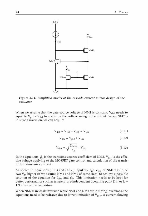
Figure 3.11: Simplified model of the cascode current mirror design of theoscillator.
When we assume that the gate-source voltage of NM1 is constant, Vds1 needs toequal to Vgs1 − Vth1 to maximize the voltage swing of the output. When NM2 isin strong inversion, we can acquire
Vds1 = Vgs1 − Vth1 = Vgs2 (3.11)
Vgs2 = Vgt2 + Vth2 (3.12)
Vds1 =
√2Ibias
β2+ Vth2. (3.13)
In the equations, β2 is the transconductance coefficient of NM2. Vgt2 is the effec-tive voltage applying to the MOSFET gate control and calculation of the transis-tor’s drain-source current.
As shown in Equations (3.11) and (3.12), input voltage Vgs1 of NM1 has to betwo Vth higher (if we assume NM1 and NM2 of same sizes) to achieve a possiblesolution of the equation for Ibias and β2. This limitation needs to be kept forbetter performance such as temperature-independent operating point [14] or low1/f noise of the transistors.
When NM2 is in weak inversion while NM1 and NM3 are in strong inversions, theequations need to be redrawn due to lower limitation of Vgs2. A current flowing
3.3 Current mode oscillator 25
through a weak inversion transistor has the equation as shown in [15]
ID = I0 × eVGSζVT . (3.14)
Then Equation (3.11) can be redrawn
Vds1 = Vgs1 − Vth1 = Vgs2 = ζVth2 × ln(Ibias
I0). (3.15)
This condition can be fulfilled with any Vgs1 larger than Vth if the devices are ofthe same size.
Output swing limitation of the regulated cascode current mirror structure is thatVds1 has to be no lower than one threshold voltage to maintain the feedback ofthe MOSFETs. Hence the lower bound for the output voltage is
Vout,min = Vth2 + Vdsat3. (3.16)
In the equation, Vth2 is referred to the threshold voltage of NM2 and Vdsat3 isreferred to the drain-source voltage of NM3 when it is in saturation region.
This structure is not fully supply independent due to the slight change in Vgs2.This change occurs because of the variation in the drain current of NM2.
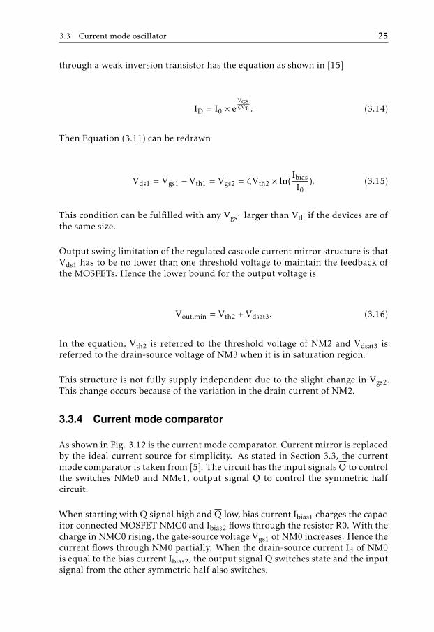
3.3.4 Current mode comparator
As shown in Fig. 3.12 is the current mode comparator. Current mirror is replacedby the ideal current source for simplicity. As stated in Section 3.3, the currentmode comparator is taken from [5]. The circuit has the input signals Q to controlthe switches NMe0 and NMe1, output signal Q to control the symmetric halfcircuit.
When starting with Q signal high and Q low, bias current Ibias1 charges the capac-itor connected MOSFET NMC0 and Ibias2 flows through the resistor R0. With thecharge in NMC0 rising, the gate-source voltage Vgs1 of NM0 increases. Hence thecurrent flows through NM0 partially. When the drain-source current Id of NM0is equal to the bias current Ibias2, the output signal Q switches state and the inputsignal from the other symmetric half also switches.
26 3 Theory
NMe0
NMC0
NM0
R0
NMe1
Ibias1 Ibias2
1.8 V
Q
Q
Q
Figure 3.12: Current mode comparator design of the proposed oscillator.
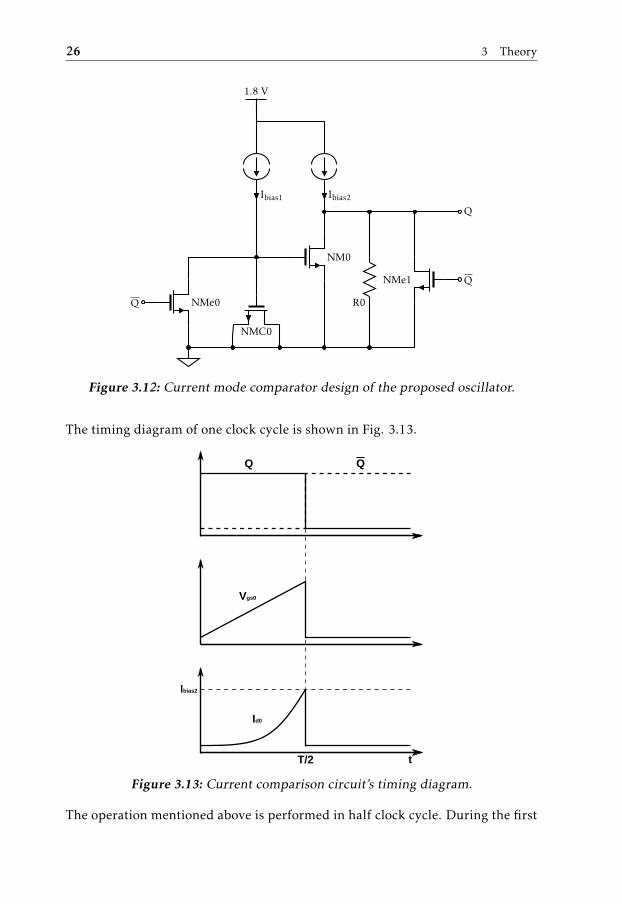
The timing diagram of one clock cycle is shown in Fig. 3.13.
Q Q
Vgs0
Id0
Ibias2
T/2 t
Figure 3.13: Current comparison circuit’s timing diagram.
The operation mentioned above is performed in half clock cycle. During the first
3.4 Temperature coefficient 27
half clock cycle, NMC0 is charged by the bias current Ibias1. Hence Vgs0 can beexpressed as a function of Tcycle, CNMC0 and Ibias1
Q =Tcycle × Ibias1
2, (3.17)
Vgs0 =Q
CNMC0, (3.18)
Vgs0 =Ibias1 × Tcycle
2CNMC0. (3.19)
By rearranging the equation we can express the output frequency as
fclk =1
Tcycle=
Ibias1
2Vgs0 × CNMC0. (3.20)
This indicates the main sources of the frequency variations. Hence these compo-nents require attentions during the layout to minimize the PVT effects on devices.
3.4 Temperature coefficient
The implementations of the resistors in all the designs are p+ polysilicon resistors.A total resistance R can be expressed as shown in [16]
R = RC + Rsilicide + Rbulk ×LW
+ Rinterface ×W0
W. (3.21)
In Equation (3.21), RC and Rsilicide are the effective contact and silicide resistance,L and W are the length and width of polysilicon resistors, respectively. W0 is anormalization constant (e.g. = 1 µm) to guarantee the right dimensions of the fullequation. As illustrated in [17], in a p+ polysilicon application, the Rbulk and theRinterface decreases with the increase of temperature. Detailed affecting factorsto the different resistor consisting components are illustrated in [18]. The TCRis dominated by the TCR values of Rbulk and Rinterface, and the total TCR can beexpressed as
TCR =1RdRdT
≈ 1W× 1
R× [(
∂Rbulk∂T
× L) + (∂Rinterf ace
∂T×W0)]. (3.22)
Clearly, TCR is maily determined by Rbulk and Rinterface of the p+ polysiliconresistor.
28 3 Theory
3.5 Noise
An ideal oscillator produces a perfectly-periodic output. In reality, however, thenoise of the oscillator devices randomly perturbs the zero crossings. A smallrandom phase quantity φn(t) can be used to describe the deviations to the idealzero crossings. The term φn(t) is called the "phase noise" [19].
Since the phase noise falls at frequencies farther from fclk, it must be specified ata certain "frequency offset," i.e., a certain difference with respect to fclk. A 1-Hzbandwidth of the spectrum at an offset of ∆f is considered, measure the powerin this bandwidth, and normalize the result to the "carrier power." The carrierpower can be viewed as the peak of the spectrum or as the power of A2/2. ’A’ inthe expression is the amplitude of the clock signal [19].
3.6 Conclusion
This chapter described the given oscillator and the proposed oscillator in detail.Some concerns regarding the oscillator stability are explained in order to betterunderstand the simulation results later in Chapter 5. As stated in Section 2.4, themain focus of this thesis is reducing the frequency standard deviation across PVTcorners to less than 6 MHz.
As stated in [20], comparators in the oscillator contribute to the frequency stan-dard deviation of oscillators. Hence a simple structure of a comparator is pre-ferred. The proposed current mode oscillator uses single MOSFET to function asa comparator. The compared signal is current instead of voltage, which helps toimprove the stability of the oscillator. As shown in [5], a current mode oscillatorcan achieve low frequency standard deviation across PVT corners.
4Method
The implementations of the designs use 0.18 µm technology. The original oscilla-tor and the improved version are implemented in schematic level. The proposedcurrent mode oscillator is implemented in both schematic and layout. The simu-lation results of different implementations are shown respectively in Chapter 5.
During the simulation, the performances of the bias generation module and com-parators in the original design limits the possibilities to further improve the orig-inal oscillator. Hence a current mode oscillator is proposed and implemented.
4.1 Testbench
The following contents in this chapter involve the implementation and simula-tion of different oscillators. All the oscillators use the same testbench. The noisesimulation in chapter 5 picks the high frequency output to analyze the phasenoise. The connection of the testbench is shown in Fig. 4.1.
The supply source is an ideal DC voltage source and the enabling signal is imple-mented with DC source as well. The enabling signal generator has a delay timein the DC source setting to simulate the logic low disabling period of the circuit.The reference current is taken from a Verilog-A model which is a bandgap cur-rent generator producing 1 µA current. Variations for different process corners,temperatures and supply voltages are modeled inside the module.
The oscillator has a trimming code generator taken from the Cadence built inlibrary igwLib. The code generator can support up to 8 bits output. However,in these applications a maximum 5 bits are taken as the inputs of the oscillator.The trimming range for both the voltage mode oscillator and the current mode
29
30 4 Method
iBias Model
Time to Freq
Trimming Code
+−VDD
+−
+−
Iin
VSS
VDD
E
Trim
E
CK80 (fclk)
CK40
CK80,CK40 Freq80,Freq40
Trim
VDD VSS
Figure 4.1: The testbench of the oscillator.
oscillator is from −8 to 7, converted to 5 bits or 4 bits two’s complement coderespectively.
At the output stage, a frequency detector from library igwLib is used to determinethe frequency of the output waveform. The frequency detector is also used todetermine the frequency settling time.
4.2 Original oscillator
The original oscillator has a 10 ns disabling pulse to setup. The bias module andlogic module are directly controlled by the outer enabling signal. The logic mod-ule is controlled by the outer enabling signal for the reason of canceling off statecurrent consumption. Middle state signal levels will force the logic componentsto work constantly, wasting power during the circuit off period.
4.2 Original oscillator 31
The original oscillator is simulated in schematic level and the simulation resultsare shown in Chapter 2. All the specifications for the proposed design are decidedbased on the original oscillator schematic simulation results. Hence the originaloscillator’s post layout simulation will not be carried out.
The oscillator is stimulated to start working when the delayed enabling signal Eois generated from the bias module. Due to the decaps in different modules, dif-ferent components need to be charged up to start working. Thus the oscillationsettles at 2.14 µs, as shown in Fig. 4.2. The Vrc voltage driven by the trimmingcontrolled current mirror starts to oscillate after a long period of capacitor charg-ing.
0 0.5 1 1.5 2 2.5
0
0.5
1
1.5
2
Time [µs]
Vol
tage
[V]
Vrc
Eo
E
Figure 4.2: Delayed enabling signal triggers the oscillation.
As shown in Tab. 2.2, the oscillator has a deviation of 11.3 MHz at output fre-quency 85.7 MHz. The output clock signal will not be used directly. It will bedivided by 8 instead to lower the transition time as well as the frequency stan-dard deviation. Hence the requirement on frequency deviation is not that strictat high frequency output.
Noise is not a concern in this application for the reason that the samples will onlybe taken when they are settled. Jitters will not affect the performance. However,noise simulations are included in the later sections as references.
Some issues appeared during the simulation and will be discussed in the follow-
32 4 Method
ing sections. These issues are around the capacitor CRamp, involving comparator’sspeed and current mirror transistors’ working regions.
4.2.1 Start-up phenomenon
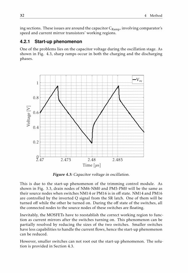
One of the problems lies on the capacitor voltage during the oscillation stage. Asshown in Fig. 4.3, sharp ramps occur in both the charging and the dischargingphases.
2.47 2.475 2.48 2.4850
0.2
0.4
0.6
0.8
1
Time [µs]
Vol
tage
[V]
Vrc
Figure 4.3: Capacitor voltage in oscillation.
This is due to the start-up phenomenon of the trimming control module. Asshown in Fig. 3.3, drain nodes of NM6-NM0 and PM5-PM0 will be the same astheir source nodes when switches NM14 or PM16 is in off state. NM14 and PM16are controlled by the inverted Q signal from the SR latch. One of them will beturned off while the other be turned on. During the off state of the switches, allthe connected nodes to the source nodes of these switches are floating.
Inevitably, the MOSFETs have to reestablish the correct working region to func-tion as current mirrors after the switches turning on. This phenomenon can bepartially resolved by reducing the sizes of the two switches. Smaller switcheshave less capabilities to handle the current flows, hence the start-up phenomenoncan be reduced.
However, smaller switches can not root out the start-up phenomenon. The solu-tion is provided in Section 4.3.
4.3 Improved oscillator 33
4.2.2 Time delay
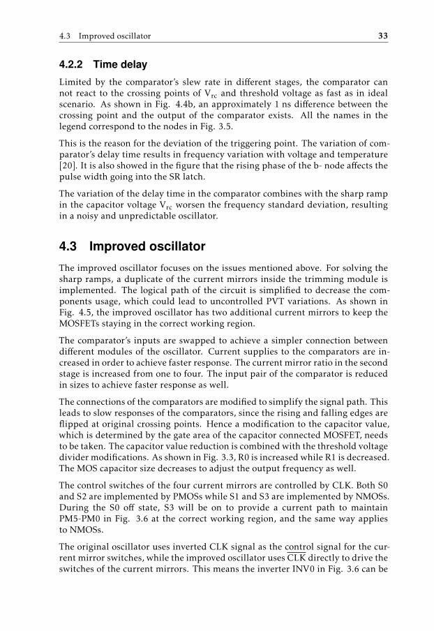
Limited by the comparator’s slew rate in different stages, the comparator cannot react to the crossing points of Vrc and threshold voltage as fast as in idealscenario. As shown in Fig. 4.4b, an approximately 1 ns difference between thecrossing point and the output of the comparator exists. All the names in thelegend correspond to the nodes in Fig. 3.5.
This is the reason for the deviation of the triggering point. The variation of com-parator’s delay time results in frequency variation with voltage and temperature[20]. It is also showed in the figure that the rising phase of the b- node affects thepulse width going into the SR latch.
The variation of the delay time in the comparator combines with the sharp rampin the capacitor voltage Vrc worsen the frequency standard deviation, resultingin a noisy and unpredictable oscillator.
4.3 Improved oscillator
The improved oscillator focuses on the issues mentioned above. For solving thesharp ramps, a duplicate of the current mirrors inside the trimming module isimplemented. The logical path of the circuit is simplified to decrease the com-ponents usage, which could lead to uncontrolled PVT variations. As shown inFig. 4.5, the improved oscillator has two additional current mirrors to keep theMOSFETs staying in the correct working region.
The comparator’s inputs are swapped to achieve a simpler connection betweendifferent modules of the oscillator. Current supplies to the comparators are in-creased in order to achieve faster response. The current mirror ratio in the secondstage is increased from one to four. The input pair of the comparator is reducedin sizes to achieve faster response as well.
The connections of the comparators are modified to simplify the signal path. Thisleads to slow responses of the comparators, since the rising and falling edges areflipped at original crossing points. Hence a modification to the capacitor value,which is determined by the gate area of the capacitor connected MOSFET, needsto be taken. The capacitor value reduction is combined with the threshold voltagedivider modifications. As shown in Fig. 3.3, R0 is increased while R1 is decreased.The MOS capacitor size decreases to adjust the output frequency as well.
The control switches of the four current mirrors are controlled by CLK. Both S0and S2 are implemented by PMOSs while S1 and S3 are implemented by NMOSs.During the S0 off state, S3 will be on to provide a current path to maintainPM5-PM0 in Fig. 3.6 at the correct working region, and the same way appliesto NMOSs.
The original oscillator uses inverted CLK signal as the control signal for the cur-rent mirror switches, while the improved oscillator uses CLK directly to drive theswitches of the current mirrors. This means the inverter INV0 in Fig. 3.6 can be
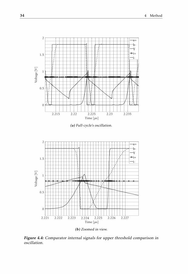
34 4 Method
2.215 2.22 2.225 2.23 2.235
0
0.5
1
1.5
2
Time [µs]
Vol
tage
[V]
a+b-Yi+i-
(a) Full-cycle’s oscillation.
2.221 2.222 2.223 2.224 2.225 2.226 2.227
0
0.5
1
1.5
2
Time [µs]
Vol
tage
[V]
a+b-Yi+i-
(b) Zoomed in view.
Figure 4.4: Comparator internal signals for upper threshold comparison inoscillation.
4.3 Improved oscillator 35
skipped. The switches NM14 and PM16 can be directly connected to the SR latchoutput CLK.
Ibias
S1
S0
Ibias
1.8 V
Ibias
Ibias
S2
S3
CRamp
−
+
−
+
CMP0
CMP1
Vrc
VthH
VthL
R
S
Q
Q
CLK
CLK
HitHigh
HitLow
ICharge
IDischarge
Figure 4.5: Improved design of the oscillator.
The improved design of the original oscillator is proposed due to the simulationresults of an intermediate implementation. By just swapping the inputs, deletingthe inverters at the output stages of the comparators and maintaining other com-ponents unchanged, the oscillator showed a nominal output frequency at 61 MHzand a frequency standard deviation of 6.8 MHz.
4.3.1 Schematic simulation
As shown in Fig. 4.7, the ramp capacitor voltage is improved without any sharpramps. Trimming control module is modified with extra current mirrors anda non-overlapping control signal generator. The non-overlapping circuit is uti-lized to avoid transparent window between switches S0, S1 and S2, S3. The non-overlapping signal generator is shown as Fig. 4.6. S0 and S2 are controlled byPhiP while S1 and S3 are controlled by PhiN. The time difference during the ris-ing phase is 128 ps, and 213 ps during the falling phase.
As shown in Fig. 4.7, the capacitor voltage exhibits a saw-tooth pattern waveform.This is achieved with the help of the duplicated current mirror in the trimmingmodule.
The internal signals of the comparator CMP0 are shown in Fig. 4.8. All thenames in the legend correspond to the nodes in Fig. 3.5. It should be noticed thatthe inputs are swapped to achieve inverted output signals from the comparators.Comparing to the original comparator, the modified comparator shows worse
36 4 Method
NOR0
NOR1
INV0INV1 INV2 INV3 INV4
INV5 INV6 INV7 INV8 INV9
DPhiN
PhiP
Figure 4.6: The non-overlapping clock generator in the improved oscillator.
2.47 2.475 2.48 2.4850
0.2
0.4
0.6
0.8
1
Time [µs]
Vol
tage
[V]
Vrc
Figure 4.7: The ramp capacitor voltage Vrc in oscillation.
4.3 Improved oscillator 37
2.425 2.43 2.435 2.44 2.445
0
0.5
1
1.5
2
Time [µs]
Vol
tage
[V]
a+b-Yi+i-
Figure 4.8: Internal signals of the VthH comparator in the improved oscilla-tor.
performance in the perspective of output time delay. A simple conclusion couldbe drawn from the waveform that the slew rate limitation in the rising edge is thereason of the worse time delay. It is clear that the falling edge at the output of theoriginal comparator is steeper than the rising edge of the improved comparator.
In the simulation section in Section 5.2, the worsened time delay of the compara-tor does not worsen the frequency standard deviation. Further discussion will bepresented in Section 6.5.
4.3.2 Limitations
The improved oscillator exhibits a good frequency standard deviation controlwhen the output frequency is around 60 MHz. The standard deviation is 6.8 MHzat output frequency 61 MHz. However, The frequency standard deviation willrise to 8.5 MHz when the output frequency is increased to 79.2 MHz with smallercapacitor and changed thresholds.
In order to find out the theoretical performance limitation of the oscillator, thecapacitor connected MOSFET CRamp is replaced by an ideal capacitor in the Ca-dence default library analoglib. The frequency standard deviation drops to 7.8 MHz,which does not meet the specification. A conclusion can be drawn that the fre-quency standard deviation comes from other modules in the oscillator, most prob-ably from bias generation module. This assumption is confirmed by the noisesimulation later.
38 4 Method
The original and improved oscillators are based on the conventional comparatordesign, which are proved hard to be further improved. This kind of RC oscillatoris limited by the comparator and passive components design. Based on capaci-tor connected MOSFET and p+ polysilicon resistor, a current mode oscillator isproposed and implemented based on the requirement on the frequency standarddeviatio.
4.4 Current mode oscillator
A current mode circuit is able to operate faster than a voltage mode circuit [21],and effects of the comparator’s non-idealities can be minimized. The clock fre-quency changes due to the comparator’s non-idealities such as offset voltage andfinite delay time. Therefore, it is difficult to obtain a stable clock frequency whenwe consider the effects of PVT variations [5]. Hence a current mode oscillatoris proposed and implemented in order to minimize the comparators’ variations.Consequently, achieving the specification of low frequency standard deviation athigh frequency output.
4.4.1 Implementation
The reference current input is generated by a bandgap device, which is not in-cluded in the design. Resistors are implemented with poly-silicon and capacitorsare implemented with capacitor connected MOSFETs.
The capacitor value of NMC0 should consist dominantly of its own parasitic ca-pacitors. This requires that the size of NMC0 should be large enough in compari-son to NM0, as shown in Fig. 3.12.
This application is designed to have an output frequency of 80 MHz, unlike itsprototype in [5], which operates at 32 MHz. Hence the bias currents are modifiedto satisfy the specification as well as stabilization. Ibias1 : Ibias2 is set to 1 : 2.
The CMC module is highly symmetric, hence the devices of this module are re-quired to place close to each other to minimize the mismatches during the layoutphase. Analog signal wires are better placed far from fast changing digital signalwires, which disrupt the analog signals during the transmission.
The p+ polysilicon resistors’ values are estimated to be 135.6 kΩ with the sizesof 20 segments of 20 µm long and 1 µm wide, spacing between segments 250 nm.Size of NM0 is 2 µm width and 0.4 µm length.
The size of NMC0 is 6.9 µm width and length. NMC0 is approximately 60 timeslarger than NM0 in area, which makes the capacitor is dominantly decided byNMC0. Switches in the CMC module for Q and Q signals are 1 µm wide and0.5 µm long. Reset switches have sizes of 0.5 µm widths and lengths.
For the bias generation module, all the NMOSs and PMOSs in the current mirrorshave the sizes of 2 µm width and 2 µm length. Switches in the bias module are1 µm wide and 1 µm long.
4.4 Current mode oscillator 39
Inverters in the design are implemented with a pair of NMOS and PMOS. Thesize of NMOS is 460 nm width and 180 nm length, while the size of PMOS is985 nm width and 180 nm length. Other digital components are shown later inthe layout part.
4.4.2 Schematic simulation
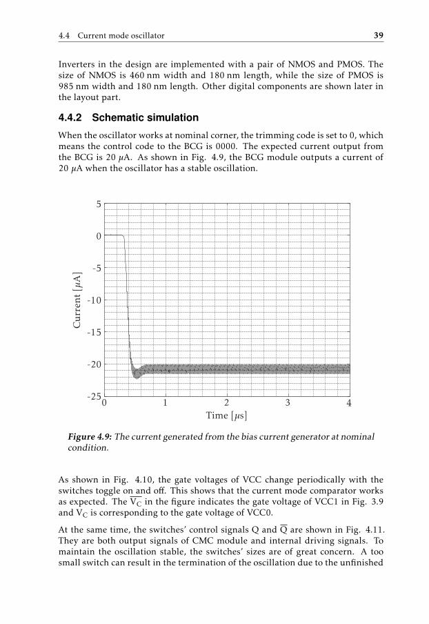
When the oscillator works at nominal corner, the trimming code is set to 0, whichmeans the control code to the BCG is 0000. The expected current output fromthe BCG is 20 µA. As shown in Fig. 4.9, the BCG module outputs a current of20 µA when the oscillator has a stable oscillation.
0 1 2 3 4-25
-20
-15
-10
-5
0
5
Time [µs]
Cu
rren
t[µ
A]
Figure 4.9: The current generated from the bias current generator at nominalcondition.
As shown in Fig. 4.10, the gate voltages of VCC change periodically with theswitches toggle on and off. This shows that the current mode comparator worksas expected. The VC in the figure indicates the gate voltage of VCC1 in Fig. 3.9and VC is corresponding to the gate voltage of VCC0.
At the same time, the switches’ control signals Q and Q are shown in Fig. 4.11.They are both output signals of CMC module and internal driving signals. Tomaintain the oscillation stable, the switches’ sizes are of great concern. A toosmall switch can result in the termination of the oscillation due to the unfinished
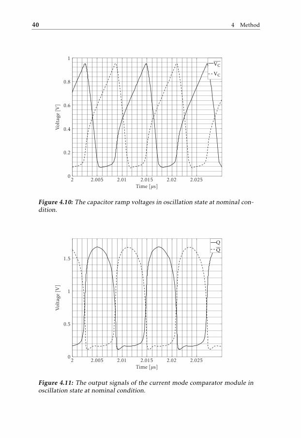
40 4 Method
2 2.005 2.01 2.015 2.02 2.0250
0.2
0.4
0.6
0.8
1
Time [µs]
Vol
tage
[V]
VC
VC
Figure 4.10: The capacitor ramp voltages in oscillation state at nominal con-dition.
2 2.005 2.01 2.015 2.02 2.0250
0.5
1
1.5
Time [µs]
Vol
tage
[V]
Figure 4.11: The output signals of the current mode comparator module inoscillation state at nominal condition.
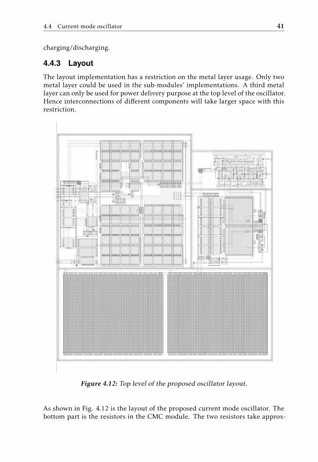
4.4 Current mode oscillator 41
charging/discharging.
4.4.3 Layout
The layout implementation has a restriction on the metal layer usage. Only twometal layer could be used in the sub-modules’ implementations. A third metallayer can only be used for power delivery purpose at the top level of the oscillator.Hence interconnections of different components will take larger space with thisrestriction.
Figure 4.12: Top level of the proposed oscillator layout.
As shown in Fig. 4.12 is the layout of the proposed current mode oscillator. Thebottom part is the resistors in the CMC module. The two resistors take approx-
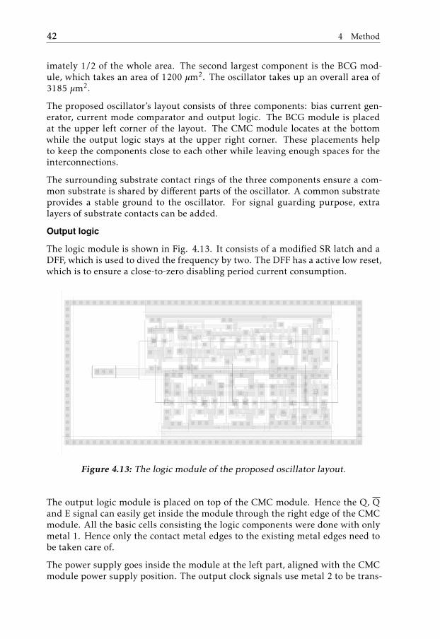
42 4 Method
imately 1/2 of the whole area. The second largest component is the BCG mod-ule, which takes an area of 1200 µm2. The oscillator takes up an overall area of3185 µm2.
The proposed oscillator’s layout consists of three components: bias current gen-erator, current mode comparator and output logic. The BCG module is placedat the upper left corner of the layout. The CMC module locates at the bottomwhile the output logic stays at the upper right corner. These placements helpto keep the components close to each other while leaving enough spaces for theinterconnections.
The surrounding substrate contact rings of the three components ensure a com-mon substrate is shared by different parts of the oscillator. A common substrateprovides a stable ground to the oscillator. For signal guarding purpose, extralayers of substrate contacts can be added.
Output logic
The logic module is shown in Fig. 4.13. It consists of a modified SR latch and aDFF, which is used to dived the frequency by two. The DFF has a active low reset,which is to ensure a close-to-zero disabling period current consumption.
Figure 4.13: The logic module of the proposed oscillator layout.
The output logic module is placed on top of the CMC module. Hence the Q, Qand E signal can easily get inside the module through the right edge of the CMCmodule. All the basic cells consisting the logic components were done with onlymetal 1. Hence only the contact metal edges to the existing metal edges need tobe taken care of.
The power supply goes inside the module at the left part, aligned with the CMCmodule power supply position. The output clock signals use metal 2 to be trans-
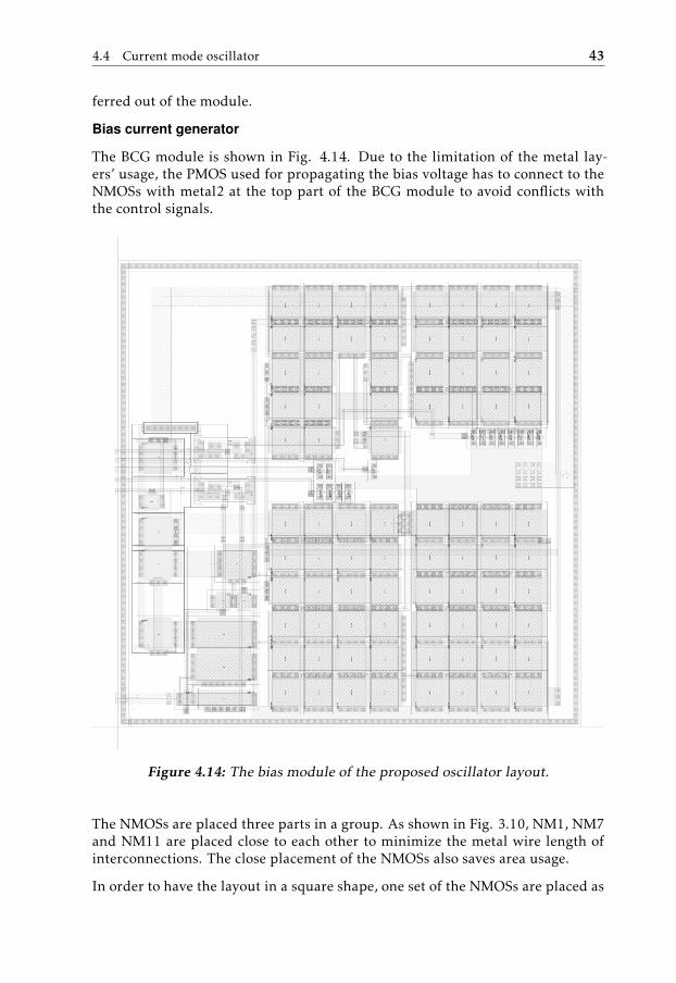
4.4 Current mode oscillator 43
ferred out of the module.
Bias current generator
The BCG module is shown in Fig. 4.14. Due to the limitation of the metal lay-ers’ usage, the PMOS used for propagating the bias voltage has to connect to theNMOSs with metal2 at the top part of the BCG module to avoid conflicts withthe control signals.
Figure 4.14: The bias module of the proposed oscillator layout.
The NMOSs are placed three parts in a group. As shown in Fig. 3.10, NM1, NM7and NM11 are placed close to each other to minimize the metal wire length ofinterconnections. The close placement of the NMOSs also saves area usage.
In order to have the layout in a square shape, one set of the NMOSs are placed as
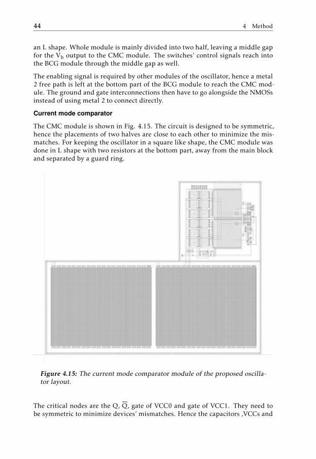
44 4 Method
an L shape. Whole module is mainly divided into two half, leaving a middle gapfor the Vb output to the CMC module. The switches’ control signals reach intothe BCG module through the middle gap as well.
The enabling signal is required by other modules of the oscillator, hence a metal2 free path is left at the bottom part of the BCG module to reach the CMC mod-ule. The ground and gate interconnections then have to go alongside the NMOSsinstead of using metal 2 to connect directly.
Current mode comparator
The CMC module is shown in Fig. 4.15. The circuit is designed to be symmetric,hence the placements of two halves are close to each other to minimize the mis-matches. For keeping the oscillator in a square like shape, the CMC module wasdone in L shape with two resistors at the bottom part, away from the main blockand separated by a guard ring.
Figure 4.15: The current mode comparator module of the proposed oscilla-tor layout.
The critical nodes are the Q, Q, gate of VCC0 and gate of VCC1. They need tobe symmetric to minimize devices’ mismatches. Hence the capacitors ,VCCs and
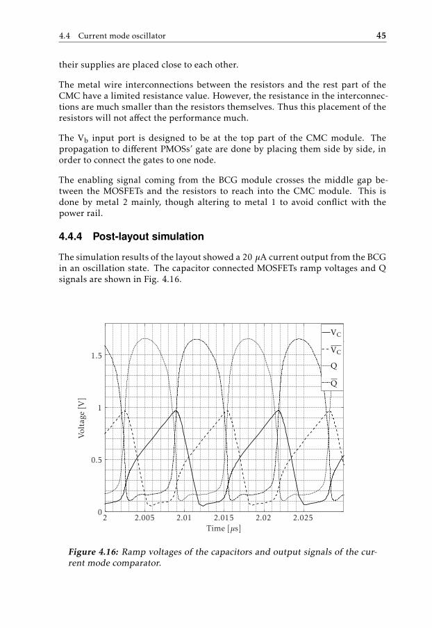
4.4 Current mode oscillator 45
their supplies are placed close to each other.
The metal wire interconnections between the resistors and the rest part of theCMC have a limited resistance value. However, the resistance in the interconnec-tions are much smaller than the resistors themselves. Thus this placement of theresistors will not affect the performance much.
The Vb input port is designed to be at the top part of the CMC module. Thepropagation to different PMOSs’ gate are done by placing them side by side, inorder to connect the gates to one node.
The enabling signal coming from the BCG module crosses the middle gap be-tween the MOSFETs and the resistors to reach into the CMC module. This isdone by metal 2 mainly, though altering to metal 1 to avoid conflict with thepower rail.
4.4.4 Post-layout simulation
The simulation results of the layout showed a 20 µA current output from the BCGin an oscillation state. The capacitor connected MOSFETs ramp voltages and Qsignals are shown in Fig. 4.16.
2 2.005 2.01 2.015 2.02 2.0250
0.5
1
1.5
Time [µs]
Vol
tage
[V]
VC
VC
Q
Q
Figure 4.16: Ramp voltages of the capacitors and output signals of the cur-rent mode comparator.

46 4 Method
The waveform indicates the layout of the proposed current mode oscillator canwork as expected. The capacitors’ voltages VC and VC are charged and dischargedperiodically.
5Result
This chapter consists of noise simulation results of different oscillator, frequencystandard deviations and VT dependeces. A comparison between different oscilla-tors’ implementations is made. Further discussions are made in Chapter 6.
This chapter first shows the nominal output frequencies and current consump-tions of different implementations. Then proceeding to VT dependences and fre-quency standard deviation with MC simulations. Thirdly, a comparison betweenthe noise simulations are included for readers who are interested in those perfor-mance parameters. Finally, a table of comparisons between different implemen-tations in different performance parameters is shown. Practical issues regardingthe given application are also shown.
Apart from the key performances of the oscillators, some practical issues are alsoof interests to be recorded. The extraction variations and the VT variations arethe two main parts. Different extractions of the layout exhibit a bit differentoutput frequencies. They should be confirmed to have a relationship of fcworst <ftypical < fcbest . Or else further investigations need to be made.
The simulations performed at nominal corner have the following settings:
• Supply voltage: 1.8 V,
• Room temperature: 25 C,
• Process corner: typical.
The current consumption measurement is described in Section 2.1, performedwith transient simulation. An average value at the ending part of the simulationis acuired for the oscillator current consumption.
47
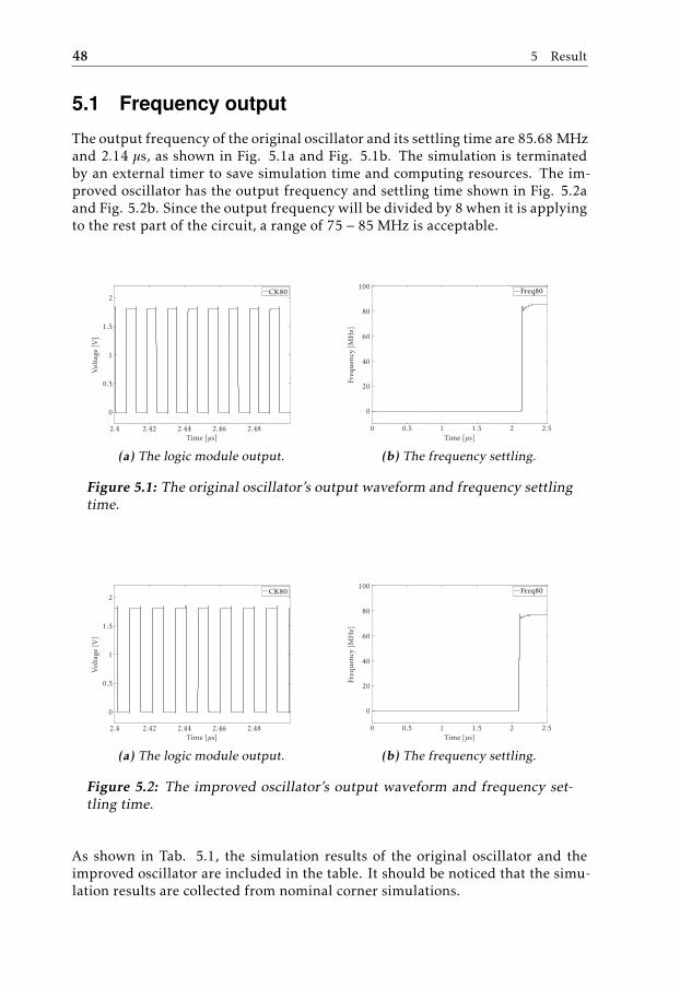
48 5 Result
5.1 Frequency output
The output frequency of the original oscillator and its settling time are 85.68 MHzand 2.14 µs, as shown in Fig. 5.1a and Fig. 5.1b. The simulation is terminatedby an external timer to save simulation time and computing resources. The im-proved oscillator has the output frequency and settling time shown in Fig. 5.2aand Fig. 5.2b. Since the output frequency will be divided by 8 when it is applyingto the rest part of the circuit, a range of 75 − 85 MHz is acceptable.
2.4 2.42 2.44 2.46 2.48
0
0.5
1
1.5
2
Time [µs]
Vol
tage
[V]
CK80
(a) The logic module output.
0 0.5 1 1.5 2 2.5
0
20
40
60
80
100
Time [µs]
Freq
uen
cy[M
Hz]
Freq80
(b) The frequency settling.
Figure 5.1: The original oscillator’s output waveform and frequency settlingtime.
2.4 2.42 2.44 2.46 2.48
0
0.5
1
1.5
2
Time [µs]
Vol
tage
[V]
CK80
(a) The logic module output.
0 0.5 1 1.5 2 2.5
0
20
40
60
80
100
Time [µs]
Freq
uen
cy[M
Hz]
Freq80
(b) The frequency settling.
Figure 5.2: The improved oscillator’s output waveform and frequency set-tling time.
As shown in Tab. 5.1, the simulation results of the original oscillator and theimproved oscillator are included in the table. It should be noticed that the simu-lation results are collected from nominal corner simulations.
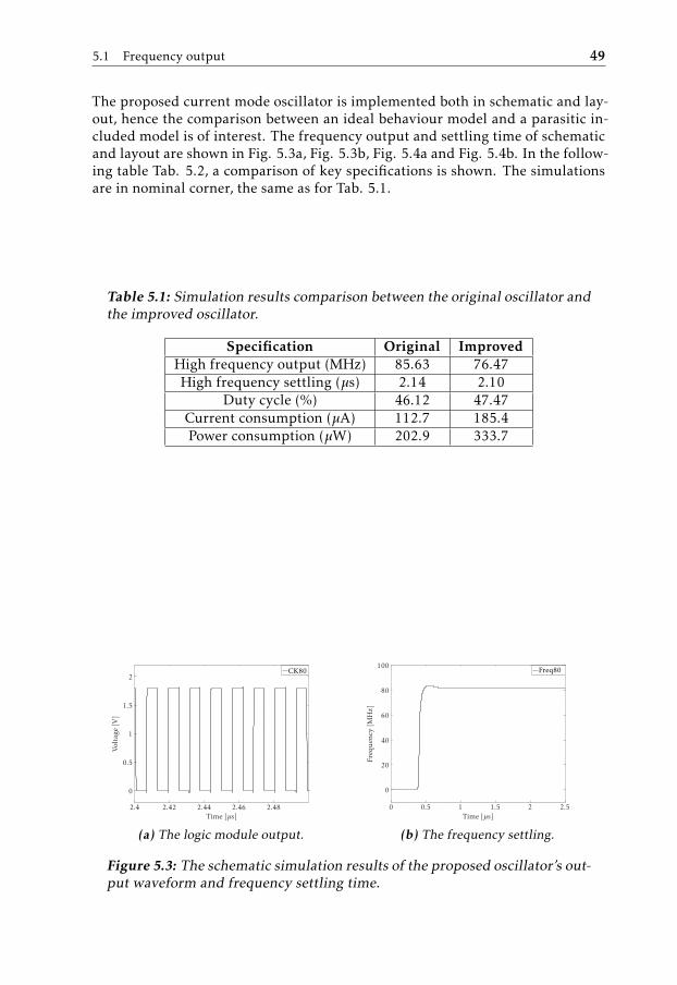
5.1 Frequency output 49
The proposed current mode oscillator is implemented both in schematic and lay-out, hence the comparison between an ideal behaviour model and a parasitic in-cluded model is of interest. The frequency output and settling time of schematicand layout are shown in Fig. 5.3a, Fig. 5.3b, Fig. 5.4a and Fig. 5.4b. In the follow-ing table Tab. 5.2, a comparison of key specifications is shown. The simulationsare in nominal corner, the same as for Tab. 5.1.
Table 5.1: Simulation results comparison between the original oscillator andthe improved oscillator.
Specification Original ImprovedHigh frequency output (MHz) 85.63 76.47High frequency settling (µs) 2.14 2.10
Duty cycle (%) 46.12 47.47Current consumption (µA) 112.7 185.4Power consumption (µW) 202.9 333.7
2.4 2.42 2.44 2.46 2.48
0
0.5
1
1.5
2
Time [µs]
Vol
tage
[V]
CK80
(a) The logic module output.
0 0.5 1 1.5 2 2.5
0
20
40
60
80
100
Time [µs]
Freq
uen
cy[M
Hz]
Freq80
(b) The frequency settling.
Figure 5.3: The schematic simulation results of the proposed oscillator’s out-put waveform and frequency settling time.
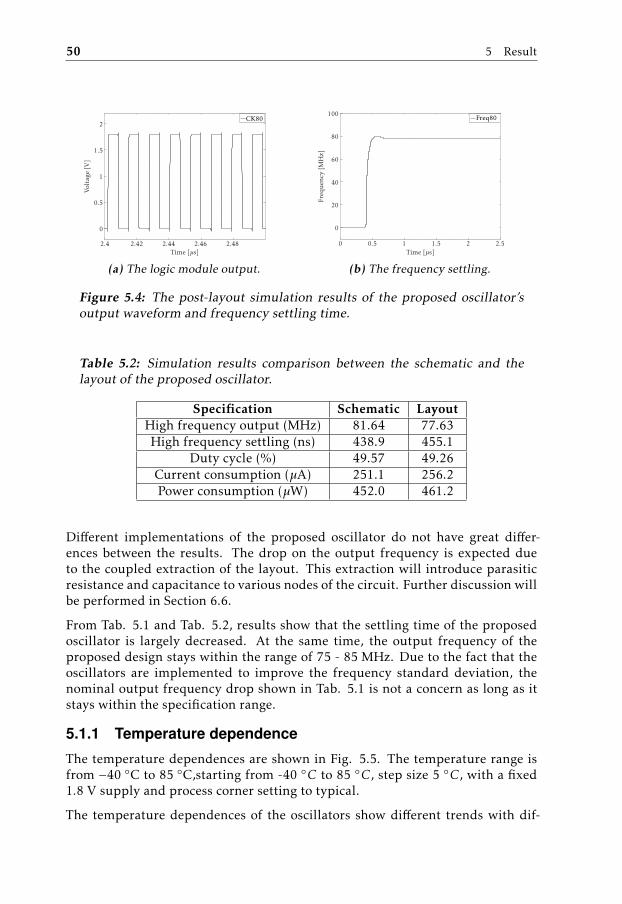
50 5 Result
2.4 2.42 2.44 2.46 2.48
0
0.5
1
1.5
2
Time [µs]
Vol
tage
[V]
CK80
(a) The logic module output.
0 0.5 1 1.5 2 2.5
0
20
40
60
80
100
Time [µs]
Freq
uen
cy[M
Hz]
Freq80
(b) The frequency settling.
Figure 5.4: The post-layout simulation results of the proposed oscillator’soutput waveform and frequency settling time.
Table 5.2: Simulation results comparison between the schematic and thelayout of the proposed oscillator.
Specification Schematic LayoutHigh frequency output (MHz) 81.64 77.63High frequency settling (ns) 438.9 455.1
Duty cycle (%) 49.57 49.26Current consumption (µA) 251.1 256.2Power consumption (µW) 452.0 461.2
Different implementations of the proposed oscillator do not have great differ-ences between the results. The drop on the output frequency is expected dueto the coupled extraction of the layout. This extraction will introduce parasiticresistance and capacitance to various nodes of the circuit. Further discussion willbe performed in Section 6.6.
From Tab. 5.1 and Tab. 5.2, results show that the settling time of the proposedoscillator is largely decreased. At the same time, the output frequency of theproposed design stays within the range of 75 - 85 MHz. Due to the fact that theoscillators are implemented to improve the frequency standard deviation, thenominal output frequency drop shown in Tab. 5.1 is not a concern as long as itstays within the specification range.
5.1.1 Temperature dependence
The temperature dependences are shown in Fig. 5.5. The temperature range isfrom −40 C to 85 C,starting from -40 C to 85 C, step size 5 C, with a fixed1.8 V supply and process corner setting to typical.
The temperature dependences of the oscillators show different trends with dif-
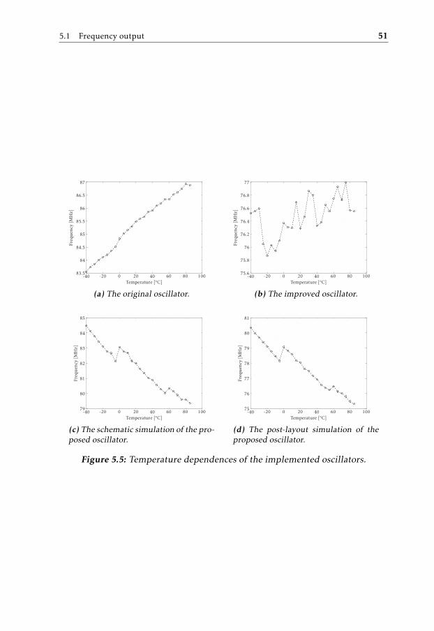
5.1 Frequency output 51
-40 -20 0 20 40 60 80 10083.5
84
84.5
85
85.5
86
86.5
87
Temperature [C]
Freq
uen
cy[M
Hz]
(a) The original oscillator.
-40 -20 0 20 40 60 80 10075.6
75.8
76
76.2
76.4
76.6
76.8
77
Temperature [C]
Freq
uen
cy[M
Hz]
(b) The improved oscillator.
-40 -20 0 20 40 60 80 10079
80
81
82
83
84
85
Temperature [C]
Freq
uen
cy[M
Hz]
(c) The schematic simulation of the pro-posed oscillator.
-40 -20 0 20 40 60 80 10075
76
77
78
79
80
81
Temperature [C]
Freq
uen
cy[M
Hz]
(d) The post-layout simulation of theproposed oscillator.
Figure 5.5: Temperature dependences of the implemented oscillators.
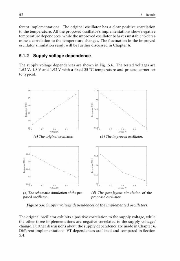
52 5 Result
ferent implementations. The original oscillator has a clear positive correlationto the temperature. All the proposed oscillator’s implementations show negativetemperature dependeces, while the improved oscillator behaves unstable to deter-mine a correlation to the temperature changes. The fluctuation in the improvedoscillator simulation result will be further discussed in Chapter 6.
5.1.2 Supply voltage dependence
The supply voltage dependences are shown in Fig. 5.6. The tested voltages are1.62 V, 1.8 V and 1.92 V with a fixed 25 C temperature and process corner setto typical.
1.6 1.7 1.8 1.9 283
84
85
86
87
88
Voltage [V]
Freq
uen
cy[M
Hz]
(a) The original oscillator.
1.6 1.7 1.8 1.9 275.5
76
76.5
77
77.5
Voltage [V]
Freq
uen
cy[M
Hz]
(b) The improved oscillator.
1.6 1.7 1.8 1.9 280.5
81
81.5
82
82.5
83
Voltage [V]
Freq
uen
cy[M
Hz]
(c) The schematic simulation of the pro-posed oscillator.
1.6 1.7 1.8 1.9 277
77.5
78
78.5
79
Voltage [V]
Freq
uen
cy[M
Hz]
(d) The post-layout simulation of theproposed oscillator.
Figure 5.6: Supply voltage dependences of the implemented oscillators.
The original oscillator exhibits a positive correlation to the supply voltage, whilethe other three implementations are negative correlated to the supply voltages’change. Further discussions about the supply dependence are made in Chapter 6.Different implementations’ VT dependences are listed and compared in Section5.4.
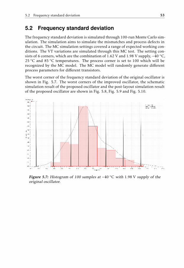
5.2 Frequency standard deviation 53
5.2 Frequency standard deviation
The frequency standard deviation is simulated through 100-run Monte Carlo sim-ulation. The simulation aims to simulate the mismatches and process defects inthe circuit. The MC simulation settings covered a range of expected working con-ditions. The VT variations are simulated through this MC test. The setting con-sists of 6 corners, which are the combination of 1.62 V and 1.98 V supply, −40 C,25 C and 85 C temperatures. The process corner is set to 100 which will berecognized by the MC model. The MC model will randomly generate differentprocess parameters for different transistors.
The worst corner of the frequency standard deviation of the original oscillator isshown in Fig. 5.7. The worst corners of the improved oscillator, the schematicsimulation result of the proposed oscillator and the post-layout simulation resultof the proposed oscillator are shown in Fig. 5.8, Fig. 5.9 and Fig. 5.10.
Figure 5.7: Histogram of 100 samples at −40 C with 1.98 V supply of theoriginal oscillator.
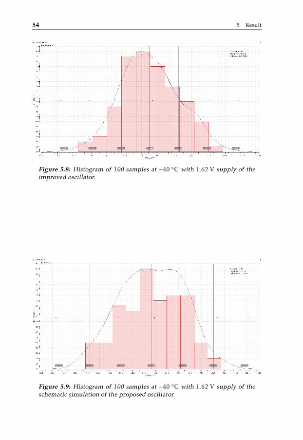
54 5 Result
Figure 5.8: Histogram of 100 samples at −40 C with 1.62 V supply of theimproved oscillator.
Figure 5.9: Histogram of 100 samples at −40 C with 1.62 V supply of theschematic simulation of the proposed oscillator.
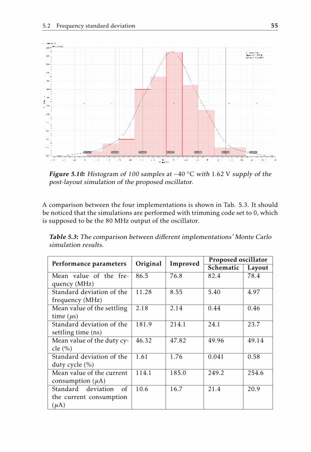
5.2 Frequency standard deviation 55
Figure 5.10: Histogram of 100 samples at −40 C with 1.62 V supply of thepost-layout simulation of the proposed oscillator.
A comparison between the four implementations is shown in Tab. 5.3. It shouldbe noticed that the simulations are performed with trimming code set to 0, whichis supposed to be the 80 MHz output of the oscillator.
Table 5.3: The comparison between different implementations’ Monte Carlosimulation results.
Performance parameters Original Improved Proposed oscillatorSchematic Layout
Mean value of the fre-quency (MHz)
86.5 76.8 82.4 78.4
Standard deviation of thefrequency (MHz)
11.28 8.55 5.40 4.97
Mean value of the settlingtime (µs)
2.18 2.14 0.44 0.46
Standard deviation of thesettling time (ns)
181.9 214.1 24.1 23.7
Mean value of the duty cy-cle (%)
46.32 47.82 49.96 49.14
Standard deviation of theduty cycle (%)
1.61 1.76 0.041 0.58
Mean value of the currentconsumption (µA)
114.1 185.0 249.2 254.6
Standard deviation ofthe current consumption(µA)
10.6 16.7 21.4 20.9
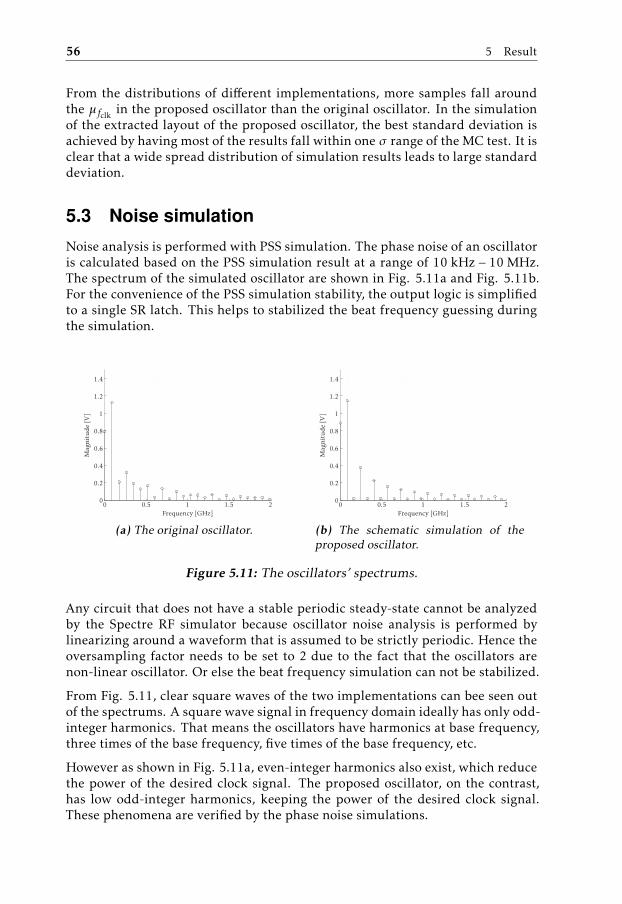
56 5 Result
From the distributions of different implementations, more samples fall aroundthe µfclk
in the proposed oscillator than the original oscillator. In the simulationof the extracted layout of the proposed oscillator, the best standard deviation isachieved by having most of the results fall within one σ range of the MC test. It isclear that a wide spread distribution of simulation results leads to large standarddeviation.
5.3 Noise simulation
Noise analysis is performed with PSS simulation. The phase noise of an oscillatoris calculated based on the PSS simulation result at a range of 10 kHz − 10 MHz.The spectrum of the simulated oscillator are shown in Fig. 5.11a and Fig. 5.11b.For the convenience of the PSS simulation stability, the output logic is simplifiedto a single SR latch. This helps to stabilized the beat frequency guessing duringthe simulation.
0 0.5 1 1.5 20
0.2
0.4
0.6
0.8
1
1.2
1.4
Frequency [GHz]
Mag
nitu
de
[V]
(a) The original oscillator.
0 0.5 1 1.5 20
0.2
0.4
0.6
0.8
1
1.2
1.4
Frequency [GHz]
Mag
nitu
de
[V]
(b) The schematic simulation of theproposed oscillator.
Figure 5.11: The oscillators’ spectrums.
Any circuit that does not have a stable periodic steady-state cannot be analyzedby the Spectre RF simulator because oscillator noise analysis is performed bylinearizing around a waveform that is assumed to be strictly periodic. Hence theoversampling factor needs to be set to 2 due to the fact that the oscillators arenon-linear oscillator. Or else the beat frequency simulation can not be stabilized.
From Fig. 5.11, clear square waves of the two implementations can bee seen outof the spectrums. A square wave signal in frequency domain ideally has only odd-integer harmonics. That means the oscillators have harmonics at base frequency,three times of the base frequency, five times of the base frequency, etc.
However as shown in Fig. 5.11a, even-integer harmonics also exist, which reducethe power of the desired clock signal. The proposed oscillator, on the contrast,has low odd-integer harmonics, keeping the power of the desired clock signal.These phenomena are verified by the phase noise simulations.
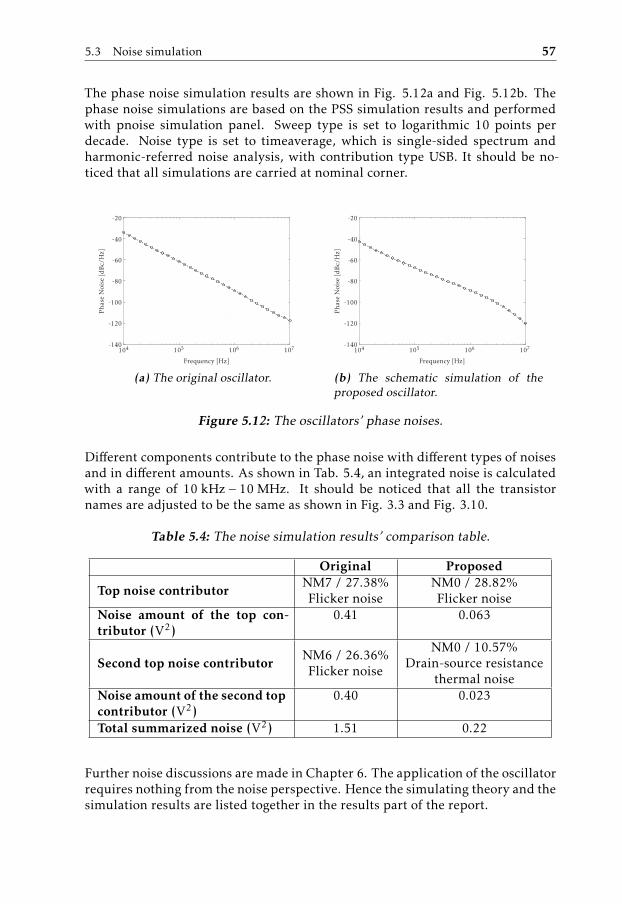
5.3 Noise simulation 57
The phase noise simulation results are shown in Fig. 5.12a and Fig. 5.12b. Thephase noise simulations are based on the PSS simulation results and performedwith pnoise simulation panel. Sweep type is set to logarithmic 10 points perdecade. Noise type is set to timeaverage, which is single-sided spectrum andharmonic-referred noise analysis, with contribution type USB. It should be no-ticed that all simulations are carried at nominal corner.
104 105 106 107-140
-120
-100
-80
-60
-40
-20
Frequency [Hz]
Pha
seN
oise
[dB
c/H
z]
(a) The original oscillator.
104 105 106 107-140
-120
-100
-80
-60
-40
-20
Frequency [Hz]
Pha
seN
oise
[dB
c/H
z]
(b) The schematic simulation of theproposed oscillator.
Figure 5.12: The oscillators’ phase noises.
Different components contribute to the phase noise with different types of noisesand in different amounts. As shown in Tab. 5.4, an integrated noise is calculatedwith a range of 10 kHz − 10 MHz. It should be noticed that all the transistornames are adjusted to be the same as shown in Fig. 3.3 and Fig. 3.10.
Table 5.4: The noise simulation results’ comparison table.
Original Proposed
Top noise contributorNM7 / 27.38%Flicker noise
NM0 / 28.82%Flicker noise
Noise amount of the top con-tributor (V2)
0.41 0.063
Second top noise contributorNM6 / 26.36%Flicker noise
NM0 / 10.57%Drain-source resistance
thermal noiseNoise amount of the second topcontributor (V2)
0.40 0.023
Total summarized noise (V2) 1.51 0.22
Further noise discussions are made in Chapter 6. The application of the oscillatorrequires nothing from the noise perspective. Hence the simulating theory and thesimulation results are listed together in the results part of the report.
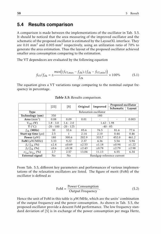
58 5 Result
5.4 Results comparison
A comparison is made between the implementations of the oscillator in Tab. 5.5.It should be noticed that the area measuring of the improved oscillator and theschematic of the proposed oscillator is estimated by the LayoutXL interface. Theyare 0.01 mm2 and 0.005 mm2 respectively, using an utilization ratio of 70% togenerate the area estimation. Thus the layout of the proposed oscillator achievedsmaller area consumption comparing to the estimation.
The VT dependeces are evaluated by the following equation
fVT/fclk = ±max
((fVT,max − fclk), (fclk − fVT,min)
)fclk
× 100% (5.1)
The equation gives a VT variations range comparing to the nominal output fre-quency in percentage.
Table 5.5: Results comparison.
[22] [5] Original Improved Proposed oscillatorSchematic Layout
Type Relaxation oscillatorTechnology (nm) 350 180
Area (mm2) 0.08 0.09 0.01 - - 0.003VDD (V) 1.8 - 3.0 1.6 - 2.0 1.62 - 1.98T (C) -20 - 100 -20 - 125 -40 - 85
fclk (MHz) 30 32.6 85.6 76.5 81.6 77.6Start-up time (µs) 2.5 1 2.14 2.10 0.44 0.46
Power (µW) 180 300.6 202.9 333.7 452.0 461.2FoM (µW/MHz) 3.33 9.22 2.37 4.36 5.54 5.94fV/fclk (%) ±2.4 ±0.69 ±2.53 ±1.18 ±0.94 ±1.22fT/fclk (%) ±0.6 ±0.38 ±2.43 ±0.78 ±2.79 ±2.98σfclk
/µfclk(%) 2.7 2.57 13.04 11.13 6.55 6.34
External signal No No Bandgap reference current
From Tab. 5.5, different key parameters and performances of various implemen-tations of the relaxation oscillators are listed. The figure of merit (FoM) of theoscillator is defined as
FoM =Power ConsumptionOutput Frequency
. (5.2)
Hence the unit of FoM in this table is µW/MHz, which are the units’ combinationof the output frequency and the power consumption. As shown in Tab. 5.5, theproposed oscillator provide a descent FoM performance. The low frequency stan-dard deviation of [5] is in exchange of the power consumption per mega Hertz,
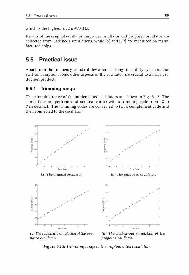
5.5 Practical issue 59
which is the highest 9.22 µW/MHz.
Results of the original oscillator, improved oscillator and proposed oscillator arecollected from Cadence’s simulations, while [5] and [22] are measured on manu-factured chips.
5.5 Practical issue
Apart from the frequency standard deviation, settling time, duty cycle and cur-rent consumption, some other aspects of the oscillator are crucial to a mass pro-duction product.
5.5.1 Trimming range
The trimming range of the implemented oscillators are shown in Fig. 5.13. Thesimulations are performed at nominal corner with a trimming code from −8 to7 in decimal. The trimming codes are converted to two’s complement code andthen connected to the oscillator.
-8 -6 -4 -2 0 2 4 660
70
80
90
100
110
Trim Code
Freq
uen
cy[M
Hz]
(a) The original oscillator.
-8 -6 -4 -2 0 2 4 660
65
70
75
80
85
90
Trim Code
Freq
uen
cy[M
Hz]
(b) The improved oscillator.
-8 -6 -4 -2 0 2 4 650
60
70
80
90
100
110
Trim Code
Freq
uen
cy[M
Hz]
(c) The schematic simulation of the pro-posed oscillator.
-8 -6 -4 -2 0 2 4 650
60
70
80
90
100
Trim Code
Freq
uen
cy[M
Hz]
(d) The post-layout simulation of theproposed oscillator.
Figure 5.13: Trimming range of the implemented oscillators.
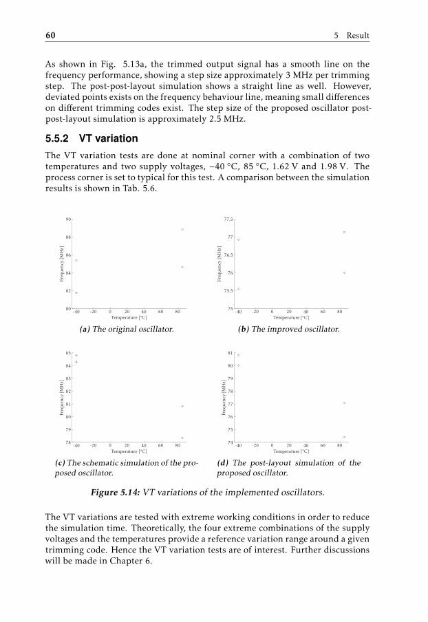
60 5 Result
As shown in Fig. 5.13a, the trimmed output signal has a smooth line on thefrequency performance, showing a step size approximately 3 MHz per trimmingstep. The post-post-layout simulation shows a straight line as well. However,deviated points exists on the frequency behaviour line, meaning small differenceson different trimming codes exist. The step size of the proposed oscillator post-post-layout simulation is approximately 2.5 MHz.
5.5.2 VT variation
The VT variation tests are done at nominal corner with a combination of twotemperatures and two supply voltages, −40 C, 85 C, 1.62 V and 1.98 V. Theprocess corner is set to typical for this test. A comparison between the simulationresults is shown in Tab. 5.6.
-40 -20 0 20 40 60 8080
82
84
86
88
90
Temperature [C]
Freq
uen
cy[M
Hz]
(a) The original oscillator.
-40 -20 0 20 40 60 8075
75.5
76
76.5
77
77.5
Temperature [C]
Freq
uen
cy[M
Hz]
(b) The improved oscillator.
-40 -20 0 20 40 60 8078
79
80
81
82
83
84
85
Temperature [C]
Freq
uen
cy[M
Hz]
(c) The schematic simulation of the pro-posed oscillator.
-40 -20 0 20 40 60 8074
75
76
77
78
79
80
81
Temperature [C]
Freq
uen
cy[M
Hz]
(d) The post-layout simulation of theproposed oscillator.
Figure 5.14: VT variations of the implemented oscillators.
The VT variations are tested with extreme working conditions in order to reducethe simulation time. Theoretically, the four extreme combinations of the supplyvoltages and the temperatures provide a reference variation range around a giventrimming code. Hence the VT variation tests are of interest. Further discussionswill be made in Chapter 6.
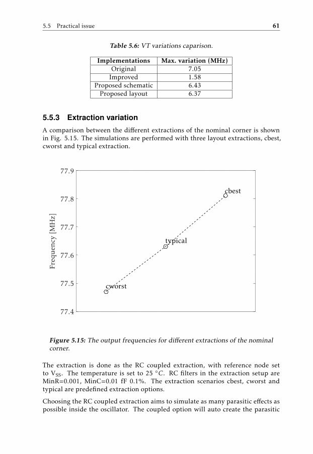
5.5 Practical issue 61
Table 5.6: VT variations caparison.
Implementations Max. variation (MHz)Original 7.05
Improved 1.58Proposed schematic 6.43
Proposed layout 6.37
5.5.3 Extraction variation
A comparison between the different extractions of the nominal corner is shownin Fig. 5.15. The simulations are performed with three layout extractions, cbest,cworst and typical extraction.
77.4
77.5
77.6
77.7
77.8
77.9
Freq
uen
cy[M
Hz]
cworst
typical
cbest
Figure 5.15: The output frequencies for different extractions of the nominalcorner.
The extraction is done as the RC coupled extraction, with reference node setto VSS. The temperature is set to 25 C. RC filters in the extraction setup areMinR=0.001, MinC=0.01 fF 0.1%. The extraction scenarios cbest, cworst andtypical are predefined extraction options.
Choosing the RC coupled extraction aims to simulate as many parasitic effects aspossible inside the oscillator. The coupled option will auto create the parasitic

62 5 Result
resistors and capacitors between different layers. Unlike decoupled extraction,which only create the parasitic between different layers and ground. In the de-coupled extraction, cross-talk problems caused by coupling parasitic caps cannotbe detected.
The differences between different extractions are ignored considering the outputfrequencies are approximately 400 times the difference. Hence all post-layoutsimulations are performed with the typical extraction of the layout.

6Discussion
This chapter consis ts of discussions related to the methods and results of theimplemented oscillator. Design considerations and brief conclusions are parts ofthe chapter as well.
Issues occurred during the project work will be mentioned as reminders when areproduction of the work is needed.
6.1 Method
This project consists of several stages. The given oscillator was analyzed first tounderstand basic principles of a relaxation oscillator. The trimming system, asthe special component of the given oscillator, needed to be kept in the proposeddesign in order to cooperate with the existing application.
Improvements based on the given oscillator were then done. Failing to achievethe frequency standard deviation specification, the improved version of the givenoscillator was discarded. While trying to simplify the comparator structure andtargeting low frequency standard deviation, a reference using current mode os-cillator with low frequency standard deviation was found on IEEE library. Hencethe proposed oscillator followed the current mode oscillator design to fulfill thefrequency standard deviation specification.
Post-layout simulations proved that the proposed oscillator based on [5] improvedoutput frequency standard deviation, but not as promising as the reference. Thisis due to the output frequency difference between this project and the reference.At last, the proposed current mode oscillator managed to achieve most of thespecifications, with a bit higher current consumption.
63
64 6 Discussion
The proposed current mode oscillator has small area consumption while main-tains stable output frequency across all PVT corners. The simulations of the pro-posed oscillator are based on the typical scenario coupled RC extraction withaccuracy of MinR=0.001, MinC=0.01 fF 0.1%. The post-layout simulation resultsbased on this extraction are the most accurate performance parameters one canacquire before the design is actually manufactured.
The MC simulations can have more points per run to acquire higher accuracy inthe output frequency distributions. However, the original designer of the givenoscillator claims that 100-points MC simulations are good enough to simulatethe oscillator output frequency spreading. Hence I followed the initial setup ofthe MC simulations. Later on, a 100-points MC simulation with 6 points to becovered takes half a day to finish the simulation, proving itself to be a time con-suming simulation. The 100-points simulation is a trade off between simulationtime and accuracy.
6.2 Noise
Although the noise performance is not of concern in this application, makingsure the sources of the noises is helpful for later work.
For conventional oscillators, the main noise sources are current sources and com-parators. Although there are oscillators with first order lag oscillation, compara-tors still remain as a significant noise source. The only way to reduce their noiseis to apply huge power (for thermal noise) and large size (for flicker noise) tocomparators; however, huge power does not match with low-power applicationsand large size of gates increases the ratio of gate parasitic capacitors includingCox which is sensitive to voltage and temperature. Of course, large parasitic ca-pacitors of comparators result in more power dissipation of oscillation [20].
The proposed current mode oscillator improves the noise performance compar-ing to the original oscillator. As shown in Tab. 5.4, the top two noise contributorschanges from two input NMOSs flicker noises to one input NMOS flicker noiseand its drain-source resistance thermal noise. The noise amount of proposedoscillator integrated within a range of 10 kHz - 10 MHz decreases 85% of theoriginal amount.
6.3 Trimming system
The oscillator uses a trimming system to ensure that PVT variations can be com-pensated. A look-up table (LUT) is created to record the trimming codes for differ-ent process corners. These codes are recorded at nominal corner. Unlike [5], thetrimming system controls the current instead of capacitors or resistors. Hencethe comparison to [5] does not use the after trimming result.
Different oscillators are tested with fixed trimming code zero for the reason ofensuring the oscillator output frequencies to be at 80 MHz. A trimming code zero
6.4 External reference 65
is located at the middle point of the trimming range. By forcing the oscillators tooutput frequency at 80 MHz, the trimming range can cover the frequency spreadshown in MC simulations.
It is due to this trimming system that the improvements to the oscillator focus onthe standard deviation. Because the process variations have been compensatedby using LUT to optimize the trimming code using. This is also the reason forthe MC settings cover the VT variations and process defects are simulated by MCmodel instead of introducing all process corners into MC simulations.
6.3.1 Trimming step
Step size of the trimming range is determined by the VT variations of the oscilla-tor in nominal process corner. The trimming step must be no larger than the VTscattering range around certain process corner, or else the trimming system cannot fulfill its duty to adjust the output frequency accordingly.
As shown in Section 5.5.1, a similar trimming step size is achieved due to thesimilarities of the trimming systems adopted in the implementations. Currentchanges for one LSB difference are similar in the proposed oscillator and the orig-inal structure. For the VT variations, the proposed oscillator has smaller VT vari-ation comparing to the original oscillator. This is verified by the smaller value offV and fT of the proposed oscillator.
6.4 External reference
To ensure the oscillator can be integrated to the existing system, an external ref-erence current is kept. This external reference current generator is modeled as aVerilog-A component. When counting the settling time of the output frequency,the start-up time of the external reference does not count in. This is the reasonwhy the oscillator designs have no start-up component for the BCG module.
6.5 Sizing
Size differences between the MOS capacitor and surrounding transistors is crucialto the oscillator dessign. Since the capacitors are implemented by MOS capacitorsin these designs, the capacitor MOSFETs sizes need to be large enough to avoidthe parasitic effects from the connected transistors.
A larger transistor has better stability over VT variations. On the other hand, thecurrent consumption, response speed and parasitic become worse as a trade off.Hence a balance between different requirements needs to be achieved.
66 6 Discussion
6.6 Improved performance of the improved oscillator
The frequency standard deviation of the improved oscillator decreased approxi-mately 3 MHz as shown in Tab. 5.3. Since the MC test contains VT variations andprocess mismatches, the results indicate that the original comparators are moreaffected by the VT variations than the improved ones.
As illustrated in Section 4.2, start-up phenomenon is the main cause for the highfrequency standard deviation of the original oscillator. Extra simulation showsthat with modified trimming control module and original comparators’ connec-tions, a frequency standard deviation of 7.75 MHz can be achieved. Which isbetter than the improved oscillator’s 8.55 MHz frequency standard deviation.
More improvements can be made to the original bias generation module to limitthe current mirror effects to the oscillator. The time limit prohibits further inves-tigation to the original oscillator.
6.7 Improved performance of post-layout simulation
After the MC simulation of extracted layout, results show a better outcome thanthe schematic one. This can be concluded to the lower output frequency of the ex-tracted view of the proposed oscillator. The introduction of the coupled parasiticcomponents lower the output frequency. Consequently, the standard deviationis reduced by the coupled extraction. The nominal corner output frequency ofthe post layout simulation drops 4 MHz and standard deviation reduces 0.5 MHzwith the MC test. This reduction of the standard deviation is hence expected.
6.8 VT dependence
The capacitor is implemented by connecting the drain, source and bulk of a MOS-FET together as bottom plate of the capacitor, leaving the gate as the top plate. Acapacitor connected this way has a voltage dependence. The capacitor’s value in-creases when the supply increases. Theoretically, the oscillators will have slowercharging while in higher supply voltage. However, the start up phenomenon inthe original oscillator cancels this effect by a sharp ramp in the beginning of thecharging phase. This is achieved by the sacrifice of the duty cycle.
The resistors are placed as described in Section 3.2.1 and 3.3.2. Thanks to thelarge sizes of the voltage divider in the original oscillator, the temperature effectis minimized. The R2 resistor in Fig. 3.3 compensates the temperature variationby making the drain node of NMe2 a temperature varying node. Which resultsin the drain node of PM3 becoming temperature varying as well. Similar sizes ofR2 and R1 ensure the varying resistances will not affect the threshold voltages.As shown in Fig. 3.3, VthL can be expressed as a function of R0, R1 and VthH
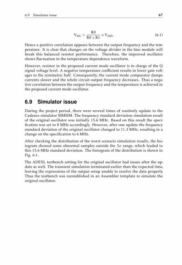
6.9 Simulator issue 67
VthL =R0
R0 + R1× VthH. (6.1)
Hence a positive correlation appears between the output frequency and the tem-perature. It is clear that changes on the voltage divider in the bias module willbreak this balanced resistor performance. Therefore, the improved oscillatorshows fluctuation in the temperature dependence waveform.
However, resistor in the proposed current mode oscillator is in charge of the Qsignal voltage level. A negative temperature coefficient results in lower gate volt-ages to the symmetric half. Consequently, the current mode comparator dampscurrents slower and the whole circuit output frequency decreases. Thus a nega-tive correlation between the output frequency and the temperature is achieved inthe proposed current mode oscillator.
6.9 Simulator issue
During the project period, there were several times of routinely update to theCadence simulator MMSIM. The frequency standard deviation simulation resultof the original oscillator was initially 15.6 MHz. Based on this result the speci-fication was set to 8 MHz accordingly. However, after one update the frequencystandard deviation of the original oscillator changed to 11.3 MHz, resulting in achange on the specification to 6 MHz.
After checking the distribution of the worst scenario simulation results, the his-togram showed some abnormal samples outside the 3σ range, which leaded tothis 15.6 MHz standard deviation. The histogram of the distribution is shown inFig. 6.1.
The ADEXL testbench setting for the original oscillator had issues after the up-date as well. The transient simulation terminated earlier than the expected time,leaving the expressions of the output setup unable to resolve the data properly.Thus the testbench was reestablished in an Assembler template to simulate theoriginal oscillator.
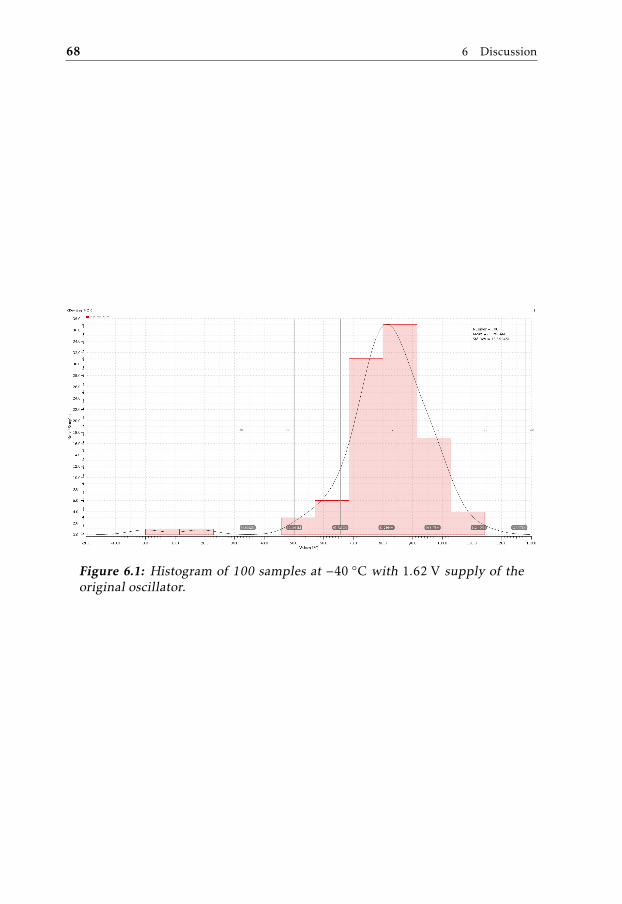
68 6 Discussion
Figure 6.1: Histogram of 100 samples at −40 C with 1.62 V supply of theoriginal oscillator.
7Conclusion and future’s work
Based on the problem statements in Section 1.2, this thesis presented two designsof the oscillator. The circuit blocks are designed and implemented in a CMOSprocess. Design considerations for the various circuits and their performancespecifications were illustrated in Chapter 2-5 and the following conclusions aredrawn.
Chapter 2 showed the simulation results of the original oscillator. Based on thesimulations results the specifications for the project are proposed. Chapter 3elaborated the theories behind different blocks of the oscillator. The workingmethod of the proposed current mode oscillator is defined. Chapter 4 illustratedthe implementation of the two oscillators. Chapter 5 presented the results ofdifferent implementations of the oscillators and comparisons between differentperformance specifications were made. A layout of a low frequency standarddeviation relaxation oscillator was designed and simulated. This current modeoscillator achieves an FoM of 5.94 µW/MHz, σ/µ of 6.34%.
This project successfully proposed and designed an oscillator which meets allthe specifications. The proposed current mode oscillator achieves low frequencystandard deviation at a high frequency output with small area usage.
7.1 Future’s work
This proposed oscillator can be integrated into, for example, a sensor, which canhelp improve mobile payment in the modern society. Biometric characteristicscan be never forgotten comparing to PIN code. A stable oscillator helps to achievefast recognition and speed up the purchase. A biometric sensor always requiresa stable and power saving oscillator.
69

70 7 Conclusion and future’s work
More works can be done to the enabling signal control switches’ implementationsand bias current generation module. A transmission gate switch or a self biasedcurrent generator with opposite temperature coefficients could be good solutionto the proposed current mode oscillator.
Extra add-on to the original oscillator is an accessible solution as well, such asself-clocked offset-cancellation [23], voltage averaging feedback [20].
Bibliography
[1] R.F. Graf. Modern Dictionary of Electronics. Newnes, seventh edition, 1999.Cited on page 1.
[2] K.L. Du and M.N.S. Swamy. Wireless Communication Systems: From RFSubsystems to 4G Enabling Technologies. Cambridge University Press, firstedition, 2010. Cited on page 1.
[3] W.A. Edson. Vacuum-tube oscillators. Wiley, first edition, 1953. Cited onpage 1.
[4] L.B. Oliveira, J. Fernandes, I.M. Filanovsky, C.J.M. Verhoeven, and M.M.Silva. Analysis and Design of Quadrature Oscillators. Springer Netherlands,first edition, 2008. Cited on page 1.
[5] H. Asano, T. Hirose, T. Miyoshi, K. Tsubaki, T. Ozaki, N. Kuroki, and M.Numa. “A fully integrated, 1-µs start-up time, 32-MHz relaxation oscillatorfor low-power intermittent systems”. In 2016 14th IEEE International NewCircuits and Systems Conference (NEWCAS), pages 1–4, June 2016. doi:10.1109/NEWCAS.2016.7604819. Cited on pages 9, 20, 25, 28, 38, 58, 59,63, and 64.
[6] T.C. Carusone, D. Johns, and K.W. Martin. Analog Integrated Circuit Design.Wiley, second edition, 2012. Cited on pages 13 and 16.
[7] I. M. Filanovsky and H. Baltes. “CMOS Schmitt trigger design”. IEEE Trans-actions on Circuits and Systems I: Fundamental Theory and Applications,41(1):46–49, 1994. Cited on page 13.
[8] P.R. Gray. Analysis and Design of Analog Integrated Circuits. John Wiley &Sons, fifth edition, 2009. Cited on pages 16 and 17.
[9] J.M. Rabaey, A.P. Chandrakasan, and B. Nikolic. Digital integrated circuits:a design perspective. Pearson Education, second edition, 2003. Cited onpage 19.
[10] M. Rakus, V. Stopjaková, and D. Arbet. “Comparison of gate-drivenand bulk-driven current mirror topologies”. In 2016 IEEE 19th Interna-
71
72 Bibliography
tional Symposium on Design and Diagnostics of Electronic Circuits Systems(DDECS), pages 1–4, April 2016. doi: 10.1109/DDECS.2016.7482457. Citedon page 21.
[11] E. Säckinger and W. Guggenbühl. “A high-swing, high-impedance MOScascode circuit”. IEEE Journal of Solid-State Circuits, 25(1):289–298, 1990.Cited on page 21.
[12] K. Bult and G.J.G.M. Geelen. “The CMOS gain-boosting technique”. AnalogIntegrated Circuits and Signal Processing, 1(2):119–135, 1991. Cited onpage 21.
[13] P. Vajpayee, A. Srivastava, S.S. Rajput, and G.K. Sharma. “Low voltage regu-lated cascode current mirrors suitable for sub-1V operation”. In 2010 IEEEAsia Pacific Conference on Circuits and Systems, pages 584–587, Dec 2010.doi: 10.1109/APCCAS.2010.5774891. Cited on page 21.
[14] R.A. Blauschild, P.A. Tucci, R.S. Muller, and R.G. Meyer. “A new NMOStemperature-stable voltage reference”. IEEE Journal of Solid-State Circuits,13(6):767–774, 1978. Cited on page 24.
[15] B. Razavi. Design of Analog CMOS Integrated Circuits. McGraw-Hill, inter-national edition, 2001. Cited on page 25.
[16] W.-C. Liu, K.-B. Thei, H.-M. Chuang, K.-W. Lin, C.-C. Cheng, Y.-S. Ho, C.-W.Su, S.-C. Wong, C.-H. Lin, and C.H. Diaz. “Characterization of polysiliconresistors in sub-0.25 µm CMOS ULSI applications”. IEEE Electron DeviceLetters, 22(7):318–320, 2001. Cited on page 27.
[17] C.-M. Uang, H.-M. Chuang, T. Shen Fu, K.-B. Thei, P.-H. Lai, S.-I. Fu, Y.-Y.Tsai, and W.-C. Liu. “Temperature-dependent characteristics of diffused andpolysilicon resistors for ULSI applications”. In Junction Technology, 2004.IWJT ’04. The Fourth International Workshop on, pages 293–296, March2004. doi: 10.1109/IWJT.2004.1306860. Cited on page 27.
[18] N.S. Alvi, S.M. Tang, R. Kwor, and M.R. Fulcher. “Recrystallization by rapidthermal annealing of implanted low-pressure chemical-vapor-depositedamorphous Si films”. Journal of Applied Physics, 62(12):4878–4883, 1987.Cited on page 27.
[19] B. Razavi. RF Microelectronics. Prentice Hall, second edition, 2012. Citedon page 28.
[20] Y. Tokunaga, S. Sakiyama, A. Matsumoto, and S. Dosho. “An on-chip CMOSrelaxation oscillator with voltage averaging feedback”. IEEE Journal ofSolid-State Circuits, 45(6):1150–1158, 2010. Cited on pages 28, 33, 64,and 70.
[21] J.H. Kim, J.B. Shin, J.Y. Sim, and H.J. Park. “5-Gb/s peak detector using acurrent comparator and a three-state charge pump”. IEEE Transactions on
Bibliography 73
Circuits and Systems II: Express Briefs, 58(5):269–273, 2011. Cited on page38.
[22] K. Ueno, T. Asai, and Y. Amemiya. “A 30-MHz, 90-ppm/C fully-integratedclock reference generator with frequency-locked loop”. In 2009 Proceed-ings of ESSCIRC, pages 392–395, Sept 2009. doi: 10.1109/ESSCIRC.2009.5325940. Cited on pages 58 and 59.
[23] K. Choe, O.D. Bernal, D. Nuttman, and M. Je. “A precision relaxationoscillator with a self-clocked offset-cancellation scheme for implantablebiomedical SoCs”. In 2009 IEEE International Solid-State Circuits Con-ference - Digest of Technical Papers, pages 402–403,403a, Feb 2009. doi:10.1109/ISSCC.2009.4977478. Cited on page 70.


Appendix


AAppendix
A.1 Opponent’s questions and respondent’sresponses
• Q1: If the oscillator should operate in only the range of 75-85 MHz, Whatis the reason to have a wide tunable frequency range?
A1: The tuning range is to cover unexpected output frequencies, which areshown in MC simulations as shown in Tab. 2.2.
• Q2: The original design consumed 112.6 µA, but the new "budget" were setto 250 µA. Maybe a table with simulations with the original design with thetrimming code set so that the oscillator are provided with this maximumcurrent could be used as a reference?
A2: Unfortunately, comparison needs to be made with same trimming codesinstead of with same current consumptions. An explanations are added inSection 6.3. One feasible way is to increase the current supply in the origi-nal oscillator while keeping the trimming codes fixed to zero.
• Q3: At page 49 in table 5.1, the results for the original and improved os-cillator is presented. The improved design consumes just above 50% morepower when operating at a frequency of about 10MHz lower than the origi-nal. Is this still considered an improvement?
A3: Yes, the improvement is firstly considered in a standard deviation per-spective. The current consumption and the nominal output frequency areless concerned as long as they are within the specifications. An expandeddescriptions are added to Section 5.1.
77

78 A Appendix
• Q4: At page 33 you state some new values for the capacitor and resistor ofthe improved implementation. How did you come up with these values?
A4: They are decided by sweeping tests in transient simulations and thevalues are shown by the schematic window.
• Q5: At page 35 there is a schematic of the improved design with compara-tors flipped, inverters removed and two additional current sources. Didyou perform any intermediate simulations, meaning simulating on only thecomparator flip and removal of the inverters without adding the currentsources?
A5: Yes, the intermediate simulations showed that the nominal output fre-quency dropped to 61 MHz, which was out of the specification range. AnMC test was also performed and the results showed that the frequency stan-dard deviation was 6.8 MHz. Extra descriptions are added in Section 4.3.
• Q6: At page 31, you say that the standard deviation of high frequencies isnot important since the generated signal should be divided by 8. Does thismean that it should actually produce a signal between 9.375 to 10.625 MHz?This is not explained why, and What is the reason for not designing anoscillator to produce this lower frequency directly instead if this is the case?
A6: Firstly, the high frequency is desired by the customer. Secondly, a highfrequency oscillator consumes less area comparing to a low frequency os-cillator. The low frequency oscillator requires large passive components,which take large area of the layout. Finally, this high frequency can bechanged to low frequency quite easily by using DFFs, leaving more controlspaces to the designers.
• Q7: At page 55 is a table with the results of the different designs. They wereall simulated at different mean frequencies. Did you try to set the trimmingcode so that they were simulated at frequencies more close to each other?
A7: The purpose of the simulations on page 55 is to check the frequencystandard deviations of different implementations with fixed trimming codes.Setting different trimming codes will deviate the middle point of the trim-ming range. Explanations are added in Section 6.3.
• Q8: At page 57 you say that the oscillator does not require anything from anoise perspective. How come that the oscillator is not affected from noise?
A8: The original designer claimed that the oscillator would only take sam-ples when the inputs are so stable that even jitters could not affect the re-sults. I followed his instruction of the oscillator application. Explanationsare added in Section 3.2.
• Q9: At page 58, two other work are used as a reference. Both of them arerunning at around 30MHz. Did you find any other work that were operat-ing at the same frequency that your oscillator are?
A.1 Opponent’s questions and respondent’s responses 79
A9: No. During my searching of the reference articles, I did not find anyrelaxation oscillators operating at 80 MHz.
• Q10: At page 66, some comments are made on an update of the simulationsoftware. Did you find out what caused this change?
A10: No, I failed to find out the reasons.
• Q11: How time consuming were the simulations? If it took a lot of timehave you any idea on how to maybe reduce this time for future reference?
A11: One MC simulations usually takes half a day to finish. A normal tran-sient simulations usually takes two minutes. Hence MC simulations can beperformed during the night time and other tests during the daytime. Bydoing so, out of office hours can also be made use of. Resource limitationsare mentioned in Section 2.2.
• Q12: At page 64 you state that it is mainly due to the fact that the oscil-lator has a tunable frequency with the trimming codes that is the reasonfor the standard deviation in frequency, but at page 65 you say that thestart-up phenomenon is the main cause for this. Which one is true and howdid you compare the two when determining which of the areas (start up ortrimming) that you should pay more attention to?
A12: The trimming system just provides an output range to cover unex-pected output frequencies. The start-up phenomenon is the true cause ofthe large standard deviation. This misunderstanding is due to the wronglyconstructed sentences in the discussion chapter. Section 6.3 has been re-vised.

80 A Appendix
A.2 Change track
Table A.1: Document history.
Version Date Changes Performed by ReviewedP1A 2017-05-30 First draft. Jianxing Dai Dr. J Jacob Wikner
P2A 2017-06-12Abstract revised.Discussion chapter expanded.Appendix added.
Jianxing Dai,Carl-Fredrik Tengberg Dr. J Jacob Wikner
P2B 2017-06-14 Appendix revised. Jianxing Dai Dr. J Jacob WiknerP3A 2017-06-15 Acknowledgments added. Jianxing Dai Dr. J Jacob Wikner