ANALYSIS AND COMPARISON OF VARIOUS … · During a transient on the input ... inverter this current...
12
International Journal of Scientific Research and Management Studies (IJSRMS) ISSN: 2349-3771 Volume 1 Issue 4, pg: 136-147 http://www.ijsrms.com ©IJSRMS pg. 136 ANALYSIS AND COMPARISON OF VARIOUS PARAMETERS FOR DIFFERENT MULTIPLIER DESIGNS Vidhi Gupta 1 , J. S. Ubhi 2 1 Scholar M.Tech (ECE), 2 Associate Professor Sant Longowal Institute of Engineering & Technology, Longowal, Punjab, India ABSTRACT A multiplier has a significant role in various arithmetic operations in digital processing applications which include digital filtering, digital communications and spectral analysis. With the advancement in semiconductor technology, chip density and operating frequency are increasing, so the power consumption in VLSI circuits has become a major problem of consideration. Designing fast and low power multipliers has long been a great theoretical and practical interest for computer scientists and engineers. In this paper the analysis of dynamic and static power is done for 4x4 Array and 4x4 Wallace tree multiplier and comparison is being done using different Logic design styles namely Conventional Static Logic (CSL), Complementary Pass transistor Logic (CPL), Double Pass transistor Logic (DPL) and Domino Logic. Noise margin and delay for various types of multipliers is also being evaluated. The work has been done in a schematic editor using Tanner tool v13 in 90nm CMOS technology. T-spice is used as simulator and W-editor is used for formal verification of the multiplier. KEY WORDS-Array Multipliers, Wallace tree Multiplier, Full adder, CMOS, CPL, DPL, Domino Logic. I. INTRODUCTION Multiplier performs multiplication process. The multipliers play a major role in arithmetic operations in digital signal processing applications. They were introduced by M. K. Ibrahim in 1993. The present day developments in the processor design tend to achieve low power multiplier architecture usage in their processor circuit. Further, the requirement for low power multiplier with reduced leakage current and high noise margin has been increased due to the increasing demand for portable and mobile systems. Therefore, the need for the low power multipliers has been increased. Many different types of low power multipliers are proposed and fabricated as benchmarks for demonstrating various high speed technologies in many applications [1-3]. Low power design techniques require special attention to avoid significant increment of the circuit’s area or sacrifice in the speed performance of the system. Multiplications are very expensive and slows the overall operation. The performance of many computational problems are often dominated by the speed at which a multiplication operation can be executed. Now, as the technology is continuously scaled, leakage currents become a major contributor to the total power dissipation [1]. A reduction in power supply voltage is necessary to reduce dynamic power and avoid reliability problems in deep sub-micron (DSM) regimes. A noise-tolerant high- performance static circuit family is suitable for low-voltage operation and hence noise margin plays an important role. There are four components of power dissipation [2] in digital CMOS circuits, as describe in equation below. P = Pdynamic switching + Pshort circuit + Pstatic biasing+ Pleakage where P is the total power dissipation, Pdynamic switching is the dynamic switching power, Pshort circuit is the short-circuit power, Pstatic–biasing is the static biasing power and
Transcript of ANALYSIS AND COMPARISON OF VARIOUS … · During a transient on the input ... inverter this current...

International Journal of Scientific Research and Management Studies (IJSRMS)
ISSN: 2349-3771 Volume 1 Issue 4, pg: 136-147
http://www.ijsrms.com ©IJSRMS pg. 136
ANALYSIS AND COMPARISON OF VARIOUS PARAMETERS
FOR DIFFERENT MULTIPLIER DESIGNS
Vidhi Gupta1, J. S. Ubhi2
1Scholar M.Tech (ECE), 2Associate Professor
Sant Longowal Institute of Engineering & Technology, Longowal, Punjab, India
ABSTRACT
A multiplier has a significant role in various arithmetic operations in digital processing applications which
include digital filtering, digital communications and spectral analysis. With the advancement in semiconductor
technology, chip density and operating frequency are increasing, so the power consumption in VLSI circuits has
become a major problem of consideration. Designing fast and low power multipliers has long been a great
theoretical and practical interest for computer scientists and engineers. In this paper the analysis of dynamic
and static power is done for 4x4 Array and 4x4 Wallace tree multiplier and comparison is being done using
different Logic design styles namely Conventional Static Logic (CSL), Complementary Pass transistor Logic
(CPL), Double Pass transistor Logic (DPL) and Domino Logic. Noise margin and delay for various types of
multipliers is also being evaluated. The work has been done in a schematic editor using Tanner tool v13 in
90nm CMOS technology. T-spice is used as simulator and W-editor is used for formal verification of the
multiplier.
KEY WORDS-Array Multipliers, Wallace tree Multiplier, Full adder, CMOS, CPL, DPL, Domino Logic.
I. INTRODUCTION
Multiplier performs multiplication process. The multipliers play a major role in arithmetic operations
in digital signal processing applications. They were introduced by M. K. Ibrahim in 1993. The present
day developments in the processor design tend to achieve low power multiplier architecture usage in
their processor circuit. Further, the requirement for low power multiplier with reduced leakage current
and high noise margin has been increased due to the increasing demand for portable and mobile
systems. Therefore, the need for the low power multipliers has been increased. Many different types
of low power multipliers are proposed and fabricated as benchmarks for demonstrating various high
speed technologies in many applications [1-3]. Low power design techniques require special attention
to avoid significant increment of the circuit’s area or sacrifice in the speed performance of the system.
Multiplications are very expensive and slows the overall operation. The performance of many
computational problems are often dominated by the speed at which a multiplication operation can be
executed. Now, as the technology is continuously scaled, leakage currents become a major contributor
to the total power dissipation [1]. A reduction in power supply voltage is necessary to reduce dynamic
power and avoid reliability problems in deep sub-micron (DSM) regimes. A noise-tolerant high-
performance static circuit family is suitable for low-voltage operation and hence noise margin plays
an important role.
There are four components of power dissipation [2] in digital CMOS circuits, as describe in equation
below.
P = Pdynamic switching + Pshort circuit + Pstatic biasing+ Pleakage
where P is the total power dissipation,
Pdynamic switching is the dynamic switching power, Pshort circuit is the short-circuit power,
Pstatic–biasing is the static biasing power and
International Journal of Scientific Research and Management Studies (IJSRMS)
ISSN: 2349-3771 Volume 1 Issue 4, pg: 136-147
http://www.ijsrms.com ©IJSRMS pg. 137
Pleakage is the leakage power.
Dynamic switching power dissipation is caused by charging capacitances in the circuit. During each
low-to-high output transition, the load capacitance CL is charged through the PMOS transistor, and a
certain amount of energy is drawn from the power supply. Part of this energy is dissipated in PMOS
device and part is stored on CL. It is discharged during the high-to-low output transition, and the
stored energy is dissipated through the NMOS transistor.
Given a gate switching frequency f, the power drawn from the supply is given by:
Pdynamic switching = CLVdd2f
Short–circuit power is the second source of total power dissipation. During a transient on the input
signal, there will be a period in which both NMOS and PMOS transistor will conduct simultaneously,
causing a current flow through the direct path existing between power supply and ground
terminals[4]. This short circuit current usually happen for very small intervals. In a static CMOS
inverter this current flows as long as the input voltage is higher than a NMOS threshold voltage above
ground and lower than a PMOS threshold voltage below the power supply. It is proportional to the
input ramp, the output load, and the transistors size. It can be approximated according to equation
Pshort circuit = K(Vdd – 2Vth)3 τ f
where K is a constant that depends on the transistors size, and on the technology parameters, Vdd is the
supply voltage, Vth is the threshold voltage, τ is the rise or fall time of the input signal and f is the
clock frequency.
Static current that flows from Vdd to ground nodes, without degraded inputs is known as leakage
power. In past technologies, the magnitude of leakage current was low and usually neglected.
However, the devices have been scaling for decades to achieve higher density, performance. As a
consequence, leakage current in the nanometer regime is becoming a significant portion of power
dissipation in CMOS circuits. These are the three major types of leakage mechanisms: subthreshold,
gate oxide and reverse-bias p-n junction leakage (band-to-band tunneling - BTBT). In addition to
these three major leakage components, there are other ones like gate-induced drain leakage (GIDL)
and punch through current. Those components can be neglected in normal modes of operation.
To suppress power consumption in low-voltage circuits, it is necessary to reduce leakage power in
both active and standby modes. Reduction in leakage current can be achieved by using both process
and circuit level techniques. At process level, leakage reduction can be achieved by controlling the
dimensions (length, oxide thickness, junction depth, etc.) and doping profile in transistor. At circuit
level, several techniques to reduce leakage consumption have been proposed in the literature.
Noise margin is the amount of noise that a CMOS circuit could withstand without compromising the
operation of circuit. Noise margin does makes sure that any signal which is logic '1' with finite noise
added to it, is still recognized as logic '1' and not logic '0' and vice versa. It is basically the difference
between signal value and the noise value. Section II will be the related work. Section III will be
design methods. Section IV will be about array multiplier. Section V will be about Wallace tree
multiplier. Section VI include simulation setup. Section VII will be simulation result. Section VIII
will contain conclusion. At last Section IX will include future scope and at the end references.
II. RELATED WORK
Goel et. al.[22] compared 4-bit CMOS multipliers. Logic style comparisons based on full adder
circuits claimed complementary pass transistor logic (CPL) to be much more power-efficient than
complementary CMOS. However, new comparisons performed on more efficient CMOS circuit
realizations and a wider range of different logic cells, as well as the use of realistic circuit
arrangements demonstrate CMOS to be superior to CPL in most cases with respect to speed, area,
power dissipation, and power-delay products.
Singh et. al.[23] design and compared multipliers using different logic styles in which 4x4
unsigned Array and Tree multiplier architecture is being designed by using 1-bit full adders
and AND2 function following various logic styles. The full adders and AND2 function have
been designed using various logic styles following a unique pattern of structure to improve
their performance in various means like less transistors, low power, minimal delay, and
increased power delay product. The various types of adders used are complementary MOS
International Journal of Scientific Research and Management Studies (IJSRMS)
ISSN: 2349-3771 Volume 1 Issue 4, pg: 136-147
http://www.ijsrms.com ©IJSRMS pg. 138
(CMOS) logic style, complementary pass-transistor (CPL) logic style and double-pass
transistor (DPL) logic style and calculated the average power, delay and power delay product.
III. DESIGN METHODS
There are a large number of CMOS logic design styles [5]. For multiplication, adder is the basic
element. The following logic design styles are used to design the full adder cell and hence the array
multiplier and the Wallace tree multiplier [6].
A. Conventional Static CMOS-CSL
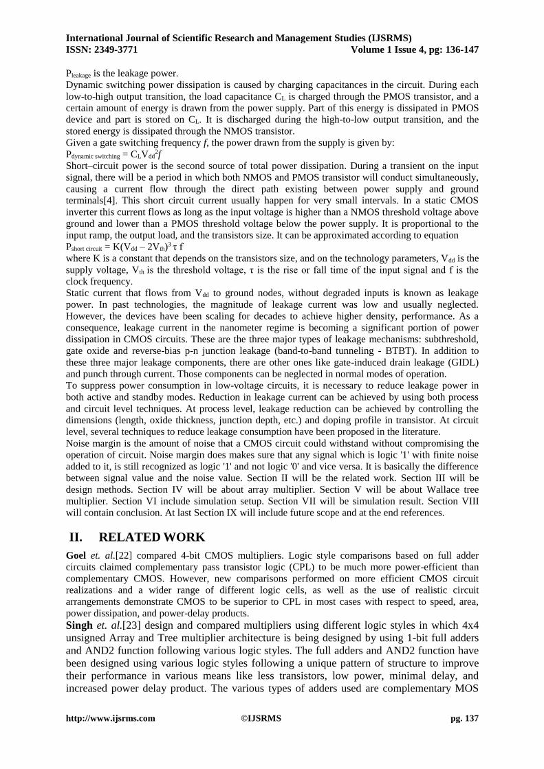
The recent VLSI arithmetic applications [6] i.e 4-bit RCA, uses conventional static CMOS logic. The
schematic diagram of a conventional static CMOS full adder cell is illustrated in figure 1. The signals
noted with ‘-’ are the complementary signals. The p- MOSFET network of each stage is the dual
network of the n- MOSFET.
Fig. 1CSL Logic Full adder
Advantages of the CMOS logic style are its robustness against voltage scaling and transistor sizing
(high noise margins) and thus reliable operation at low voltages and arbitrary (even minimal)
transistor sizes (ratio less logic).
B. Complementary Pass Transistor Logic-CPL
The basic difference of pass-transistor logic compared to the CMOS logic style is that the source side
of the logic transistor networks is connected to some input signals instead of the power lines. The
advantage is that one pass-transistor network (either NMOS or PMOS) is sufficient to perform the
logic operation, which results in a smaller number of transistors and smaller input loads, especially
when NMOS networks are used. CPL [7] uses only an n-MOSFET network for the implementation of
logic functions, thus resulting in low input capacitance and high-speed operation [8]. The schematic
diagram of the CPL full adder circuit is shown in figure 2. Because the high voltage level of the pass-
transistor outputs is lower than the supply voltage level by the threshold voltage of the pass
transistors, the signals have to be amplified by using CMOS inverters at the outputs [9].The
advantages [10] of pass logic transistors include smaller number of transistors and smaller input
loads, along with MUX and especially XOR circuits being implemented efficiently. The disadvantage
[10] of pass transistor logic is that threshold voltage drops through the NMOS transistors makes it
necessary to maintain output voltage level; hence inverter is used at output which increases the
number of transistors.

International Journal of Scientific Research and Management Studies (IJSRMS)
ISSN: 2349-3771 Volume 1 Issue 4, pg: 136-147
http://www.ijsrms.com ©IJSRMS pg. 139
Fig. 2CPL Logic Full adder
C. Double Pass Transistor Logic-DPL
DPL [11][12] is a modified version of CPL. The circuit diagram of the DPL full adder is given in
figure 3. In DPL circuit full swing operation is achieved by simply adding p- MOSFET transistors in
parallel with the n-MOSFET transistors. Hence, the problems of noise margin and speed degradation
at reduced supply voltages, which are caused in CPL circuits due to the reduced high voltage level,
are avoided.
Fig. 3 DPL Logic Full adder
The basic difference of pass-transistor logic compared to the CMOS logic style is that the source side
of the logic transistor networks is connected to some input signals instead of the power lines. The
advantage is that one pass-transistor network (either NMOS or PMOS) is sufficient to perform the
logic operation, which results in a smaller number of transistors and smaller input loads, especially
when NMOS networks are used. However, the threshold voltage drop (Vout=Vdd−Vtn) through the
NMOS transistors while passing logic “1” makes swing (or level) restoration at the gate outputs
necessary in order to avoid static currents at the subsequent output inverters or logic gates.
D. Domino Logic
Domino logic circuits have many advantages such as high speed of operation, minimum used area,
low noise margins, and the most important of all, they offer potential power consumption savings
since the overall gate capacitance is smaller than their static counterparts [21][2]. For this reason
circuit design using domino logic tends to be a very attractive method for high performance, low-

International Journal of Scientific Research and Management Studies (IJSRMS)
ISSN: 2349-3771 Volume 1 Issue 4, pg: 136-147
http://www.ijsrms.com ©IJSRMS pg. 140
power designs. The basic structure of domino logic is shown in Fig. 4. It is a non-inverting structure,
and consists of a nMOS transistor network, which implements the required logic function, two
transistors (an nMOS and a PMOS) where the clock signal is applied and synchronizes the operation
of the circuit, and a static CMOS inverter which provides the circuits output. The period where CLK
is low is called the precharge phase. In this phase the internal node, F is charged to power supply
voltage while the output node, F, is discharged to ground. The period where CLK is high is called the
evaluation phase. In this phase the values of the inputs determine the discharge (F = 0) or not (F = 1)
of the internal node. The inverter in the output of a domino logic circuit is included for several
reasons. First, it is required for proper operation of a chain of domino gates. Second, the internal node
F is a weak node, when the clock is high, the high value on that node is not driven [8].
Fig.4 Basic structure of Domino Logic
Fig 5 shows the schematic of the CARRYOUT circuit. The core of this circuit is the domino logic that
implements the function of CARRYOUT[9]. This circuit will stay in standby phase when the clock
signal CLK is logic 1. It will turn in the evaluating phase if the clock signal CLK is logic 0 .
Fig. 5 Carryout circuit of Domino Logic
For the high-speed operation, the inverter I1 is designed in multi- threshold methodology where a
low-Vt PMOS transistor is connected with a high-Vt NMOS transistor such that the logic 0 can pass
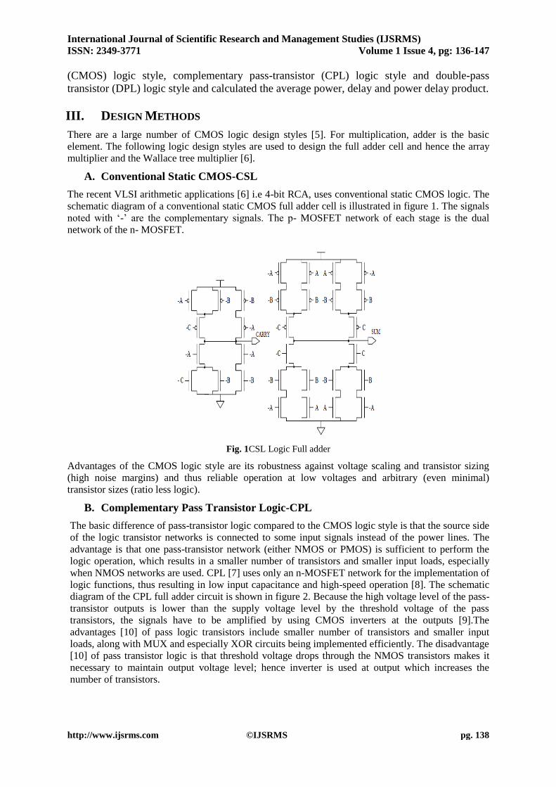
the inverter at a higher speed. Fig 6 shows the schematic of the SUM circuit. The SUM circuit is
composed of two XOR gates. The XOR gate is modified from the cross-coupled version by replacing
the NMOS portion with a clock gated NMOS. In this circuit, the PMOS transistors receive the input
signal A, B, and Cin. The operation of this circuit can be divided into two phases: the IDLE PHASE
and the EVALUATING PHASE. In the IDLE PHASE, the clock signal CLK is logic 1 and the output
signal SUM will be logic 0. In the EVALUATING PHASE, the clock signal CLK is logic 0 , and the
corresponding output signal SUM will be evaluated according to the input signals A, B, and Cin.
International Journal of Scientific Research and Management Studies (IJSRMS)
ISSN: 2349-3771 Volume 1 Issue 4, pg: 136-147
http://www.ijsrms.com ©IJSRMS pg. 141
Fig. 6 Sum circuit of Domino Logic
Fig.7 2-input AND Gate using Domino Logic
IV. ARRAY MULTIPLIER
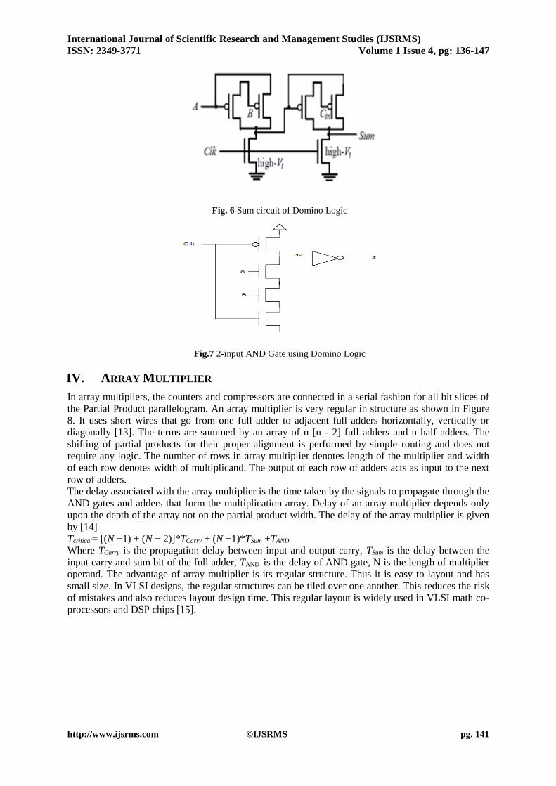
In array multipliers, the counters and compressors are connected in a serial fashion for all bit slices of
the Partial Product parallelogram. An array multiplier is very regular in structure as shown in Figure
8. It uses short wires that go from one full adder to adjacent full adders horizontally, vertically or
diagonally [13]. The terms are summed by an array of n [n - 2] full adders and n half adders. The
shifting of partial products for their proper alignment is performed by simple routing and does not
require any logic. The number of rows in array multiplier denotes length of the multiplier and width
of each row denotes width of multiplicand. The output of each row of adders acts as input to the next
row of adders.
The delay associated with the array multiplier is the time taken by the signals to propagate through the
AND gates and adders that form the multiplication array. Delay of an array multiplier depends only
upon the depth of the array not on the partial product width. The delay of the array multiplier is given
by [14]
Tcritical= [(N −1) + (N − 2)]*TCarry + (N −1)*TSum +TAND
Where TCarry is the propagation delay between input and output carry, TSum is the delay between the
input carry and sum bit of the full adder, TAND is the delay of AND gate, N is the length of multiplier
operand. The advantage of array multiplier is its regular structure. Thus it is easy to layout and has
small size. In VLSI designs, the regular structures can be tiled over one another. This reduces the risk
of mistakes and also reduces layout design time. This regular layout is widely used in VLSI math co-
processors and DSP chips [15].

International Journal of Scientific Research and Management Studies (IJSRMS)
ISSN: 2349-3771 Volume 1 Issue 4, pg: 136-147
http://www.ijsrms.com ©IJSRMS pg. 142
Fig. 8 4x4 Array Multiplier
V. WALLACE TREE MULTIPLIER
Wallace trees are irregular structure in that the informal description does not specify a systematic
method for the compressor interconnections. But still it is an efficient implementation of adding
partial products in parallel. The Wallace tree operates in three steps.
1. Multiply - each bit of multiplicand is ANDed with each bit of multiplier yielding n2 results.
Depending on the position of the multiplied bits, the wires carry different weights, for example, wire
of bit a2b3 weighs 32 [16].
2. Addition - as long as there are more than 3 wires with the same weights add a following layer. Take
3 wires of same weight and input them into a full adder. The result will be an output wire of same
weight. If there are two wires of same weight, add them using half-adder and if only one is left,
connect it to the next layer.
3. Group the wires in two numbers and add in a conventional adder.
A typical Wallace tree architecture is shown in Figure 9.
Fig. 9 4x4 Wallace tree Multiplier

International Journal of Scientific Research and Management Studies (IJSRMS)
ISSN: 2349-3771 Volume 1 Issue 4, pg: 136-147
http://www.ijsrms.com ©IJSRMS pg. 143
VI. SIMULATION SETUP
The 4x4 array multipliers and 4x4 Wallace tree multipliers are compared based on the performance
parameters like propagation delay, dynamic power dissipation, static power dissipation and noise
margin. To achieve better performance, the circuits are designed using CMOS process in 90 nm
technology. All the circuits have been designed using TANNER EDA[18].
Fig.10 CSL Full Adder
Fig.11 CPL Full Adder
Fig. 12 DPL Full Adder

International Journal of Scientific Research and Management Studies (IJSRMS)
ISSN: 2349-3771 Volume 1 Issue 4, pg: 136-147
http://www.ijsrms.com ©IJSRMS pg. 144
Fig. 13 Domino Logic Full Adder
Fig. 14 Array Multiplier
Fig. 15 Wallace tree Multiplier
VII. SIMULATION RESULT
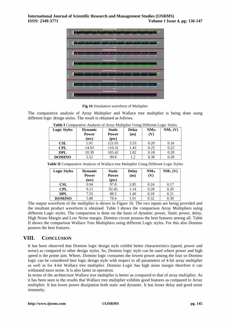
The simulation output waveform of multiplier is shown in the figure below.
International Journal of Scientific Research and Management Studies (IJSRMS)
ISSN: 2349-3771 Volume 1 Issue 4, pg: 136-147
http://www.ijsrms.com ©IJSRMS pg. 145
Fig 16 Simulation waveform of Multiplier
The comparative analysis of Array Multiplier and Wallace tree multiplier is being done using
different logic design styles. The result is obtained as follows.
Table I Comparative Analysis of Array Multiplier Using Different Logic Styles Logic Styles Dynamic
Power
(uw)
Static
Power
(pw)
Delay
(ns)
NMH
(V)
NML (V)
CSL 1.01 121.01 3.33 0.20 0.16
CPL 14.93 110.31 1.43 0.25 0.22
DPL 10.39 105.42 1.82 0.18 0.20
DOMINO 5.52 99.8 1.2 0.30 0.28
Table II Comparative Analysis of Wallace tree Multiplier Using Different Logic Styles
Logic Styles Dynamic
Power
(uw)
Static
Power
(pw)
Delay
(ns)
NMH
(V)
NML (V)
CSL 0.94 97.8 2.85 0.24 0.17
CPL 9.11 92.45 1.14 0.28 0.20
DPL 7.55 88.5 1.40 0.18 0.21
DOMINO 5.86 78.4 1.01 0.32 0.30
The output waveform of the multiplier is shown in Figure 16. The two inputs are being provided and
the resultant product waveform is obtained. Table I shows the comparison Array Multipliers using
different Logic styles. The comparison is done on the basis of dynamic power, Static power, delay,
High Noise Margin and Low Noise margin. Domino circuit possess the best features among all. Table
II shows the comparison Wallace Tree Multipliers using different Logic styles. For this also Domino
possess the best features.
VIII. CONCLUSION
It has been observed that Domino logic design style exhibit better characteristics (speed, power and
noise) as compared to other design styles. So, Domino logic style can be used where power and high
speed is the prime aim. Where, Domino logic consumes the lowest power among the four so Domino
logic can be considered best logic design style with respect to all parameters of 4-bit array multiplier
as well as for 4-bit Wallace tree multiplier. Domino Logic has high noise margin therefore it can
withstand more noise. It is also faster in operation.
In terms of the architecture Wallace tree multiplier is better as compared to that of array multiplier. As
it has been seen in the results that Wallace tree multiplier exhibits good features as compared to Array
multiplier. It has lower power dissipation both static and dynamic. It has lesser delay and good noise
immunity.

International Journal of Scientific Research and Management Studies (IJSRMS)
ISSN: 2349-3771 Volume 1 Issue 4, pg: 136-147
http://www.ijsrms.com ©IJSRMS pg. 146
IX. FUTURE SCOPE
The Future work to this research paper can be extended by designing 8-bit, 16-bit, 32-bit multipliers
using these logic design styles in 90nm technology. Another scope is to extend the work to more
advanced CMOS technology. The work can also be extended for signed and unsigned numbers.
REFERENCES
[1] G. E. Sobelman and D. L. Raatz, “Low-Power Multiplier Design Using Delayed Evaluation”, in Proc. of
IEEE International Symposium on Circuits and Systems, pp. 1564-1567, 1995.
[2] N. Weste, and K. Eshraghian, “Principles of CMOS VLSI Design”, Addison-Weslet Publishing Company,
1992.
[3] J. H. Satyanarayana and K. K. Parhi, “ A Theoretical Approach to Estimation of Bounds on Power
Consumption in Digital Multipliers”, IEEE Trans. on Circuits and Systems II, vol. 44, no. 6, pp. 473-481, June
1997.
[4] Kaushik Roy, Sharat C. Prasad, “Low-power CMOS VLSI circuit design,” Wiley-India, 2009
[5]Ila Gupta, Neha Arora, Prof.B.P.Singh, “Low Power 2:1 Multiplexer Design Using DCVS Logic and Its
Application in 1-Bit Full Adder Cell” in International Conference on Electronics and Communication
Engineering (ICECE), March 03, 2012, Bhopal, India.
[6] J. T. Yan and Z. W. Chen, “Low-power multiplier design with row and column bypassing”, IEEE
International SOC Conference, pp.227-230, 2009.
[7]Bellaouar, A., and Elmasry, M. I., Low-Power Digital VLSI Design: Circuits and Systems, Kluwer, Norwell,
MA, 1995.
[8]Parhami, B., “Computer Arithmetic –Algorithms and Hardware Designs”, Oxford University Press, 2000.
[9]Rabaey, J.M., Chandrakasan, A., and Nikolic, B.,“Digital Integrated Circuits”, Second Edition, PHI
Publishers, 2003.
[10] Ware, F.A., McAllister, W.H., Carlson, J.R., Sun, D.K., and Vlach, R.J.,“64 Bit onolithicFloating Point
Processors”, IEEE Journal of Solid-State Circuits, vol. 17, no. 5, pp. 898-90, October 1982.
[11]Parhami, B., Computer Arithmetic Algorithms and Hardware Designs, Oxford University Press, 2000.
[12] J.M., Chandrakasan, A., and Nikolic, B., Digital Integrated Circuits, Second Edition, PHI Publishers, 2003
[13] Ware, F.A., McAllister, W.H., Carlson, J.R., Sun, D.K., and Vlach, R.J., 64 Bit Monolithic Floating Point
Processors, IEEE Journal of Solid-State Circuits, vol. 17, no. 5, October 1982, pp. 898-90.
[14] C.S. Wallace, A suggestion for a fast multiplier, in IEEE Trans. On Electronic Computers, vol. EC-13,
1964, pp. 14-17.
[15] P. M. Kogge and H. S. Stone, A Parallel Algorithm for the Efficient Solution of a General Class of
Recurrence Equations, IEEE Transactions on Computers, vol. 22, no. 8, August 1973, pp. 786–793.
[16]Tanner EDA Inc. 1988, User’s Manual, 2010.
[17]Najm, F., A survey of power estimation techniques in VLSI circuits, IEEE Transactions on VLSI Systems,
vol. 2, 1995, pp. 446-455.
[18] Kang, S., Accurate simulation of power dissipation in VLSI circuits, IEEE Journal of Solid-State Circuits,
vol. 21, 1986, pp. 889-891.
[19]G. E. Sobelman and D. L. Raatz, “Low-Power Multiplier Design Using Delayed Evaluation”, in Proc. of
IEEE International Symposium on Circuits and Systems, pp. 1564-1567, 1995.
[20]N. Goel, L. Garg “Comparative Analysis of 4-bit CMOS Multipliers”, International Conference on VLSI,
Communication and Instrumentation Journal of Computer Science and Information Technology (ICVCI),
IJCSE, pp. 33-37, 2011.
[21]A. Singh, B. Prasad De, S. Maity, “Design and Comparison of Multipliers Using Different Logic Styles”,
International Journal of Soft Computing and Engineering (IJSCE), ISSN: 2231-2307, Vol. 2, Issue 2, pp. 374-
379, May 2012.
AUTHORS BIOGRAPHY
Vidhi Gupta received the B. Tech degree from Moradabad Institute of Technology, Moradabad
in 2008. She is research scholar at Sant Longowal Institute of Engineering and Technology,
Longowal. She has worked at MIT, Moradabad for four years from 2008 to 2012. She has
research interest in the field of VLSI.

International Journal of Scientific Research and Management Studies (IJSRMS)
ISSN: 2349-3771 Volume 1 Issue 4, pg: 136-147
http://www.ijsrms.com ©IJSRMS pg. 147
Jagpal Singh Ubhi received the B. E. degree and Master’s degree from Thapar Institute of
Engineering & Technology, Patiala (Punjab) in 1994 and 2000 respectively. He received his
Ph. D. degree from Punjab Technical University, Jalandhar in 2011. He is now working as a
Associate Professor at Sant Longowal Institute of Engineering and Technology, Longowal.
He is in teaching profession for the last 20 years. His current research interests include digital
communication theory, wireless fading channels, diversity systems, wireless digital
communications and VLSI design. He is life member of IE(India), IETE(India).