Analysis and Characterization of Random Skew and Jitter in ...
122
Analysis and Characterization of Random Skew and Jitter in a Novel Clock Network by Vadim Gutnik Bachelor of Science, Electrical Engineering and Computer Science, and Materials Science and Metals Engineering, University of California at Berkeley (1994) Master of Science, Electrical Engineering and Computer Science, Massachusetts Institute of Technology (1996) Submitted to the Department of Electrical Engineering and Computer Science in partial fulfillment of the requirements for the degree of Doctor of Philosophy in Electrical Engineering at the MASSACHUSETTS INSTITUTE OF TECHNOLOGY June 2000 @ Massachusetts Institute of Technology 2000. All rights reserved. Author Department of Electrical Cneering *Wt MASSACHUSETTS INSTITUTE OF TECHNOLOGY ~.j-O% JUN 2 2 2000 ...... .... LIBRARIES and Computer Science March 3, 2000 C ertified by............................... .. ......... Anantha Chandrakasan Accepted by ..... Associate- P9essor of Electrical Engineering -S ervisor Arthur C. Smith Chairman, Departmental Committee on Graduate Students
Transcript of Analysis and Characterization of Random Skew and Jitter in ...

Analysis and Characterization of Random Skew
and Jitter in a Novel Clock Network
by
Vadim Gutnik
Bachelor of Science, Electrical Engineering and Computer Science,and Materials Science and Metals Engineering,
University of California at Berkeley (1994)
Master of Science, Electrical Engineering and Computer Science,Massachusetts Institute of Technology (1996)
Submitted to the Department of Electrical Engineering and ComputerScience
in partial fulfillment of the requirements for the degree of
Doctor of Philosophy in Electrical Engineering
at the
MASSACHUSETTS INSTITUTE OF TECHNOLOGY
June 2000
@ Massachusetts Institute of Technology 2000. All rights reserved.
AuthorDepartment of Electrical Cneering
*WtMASSACHUSETTS INSTITUTE
OF TECHNOLOGY
~.j-O%JUN 2 2 2000
...... .... LIBRARIESand Computer Science
March 3, 2000
C ertified by............................... .. .........Anantha Chandrakasan
Accepted by .....
Associate- P9essor of Electrical Engineering-S ervisor
Arthur C. SmithChairman, Departmental Committee on Graduate Students


Analysis and Characterization of Random Skew and Jitter in
a Novel Clock Network
by
Vadim Gutnik
Submitted to the Department of Electrical Engineering and Computer Scienceon March 3, 2000, in partial fulfillment of the
requirements for the degree ofDoctor of Science in Electrical Engineering
Abstract
System clock uncertainty, in the form of random skew and jitter, is beginning toaffect performance of large microprocessors significantly. Process and environmentalvariations and inter-signal coupling on a chip contribute significant delay variations inlong clock lines, and these variations are predicted to make the now widely-used clocktree distribution untenable. Distributed clock generation may allow clock networksto continue scaling with advances in semiconductor processing technology.
A novel clock network composed of multiple synchronized phase-locked loops is an-alyzed, implemented, and tested. Undesirable large-signal stable (modelocked) statesdictate the transfer characteristic of the phase detectors; a matrix formulation of thelinearized system allows direct calculation of system poles for any desired oscillatorconfiguration. The circuits were fabricated in CMOS, and two implementations ofthe system - a 4 oscillator proof-of-concept 400MHz network, and a 16-oscillator,1.3GHz network network are presented.
A flash time-to-digital converter is presented that exploits parallelism to get pre-cise time measurements with resolution much smaller than a single gate delay. Unfor-tunately, an unrelated failure precluded measurements on the 16-oscillator chip wherethe measurement system was integrated, but the principle is shown to be valid on anindependent test chip.
Thesis Supervisor: Anantha ChandrakasanTitle: Associate Professor of Electrical Engineering
3

4

Acknowledgments
I would like to thank my thesis advisor, Professor Chandrakasan for innumerable
technical discussions, for always being available and approachable, and for making
sure I could concentrate on thesis work. Thanks also to my thesis readers Professors
Boning and Verghese for their help in organizing the thesis.
Thanks goes to my research group as well; my research would have been much less
enjoyable and much less successful were it not for their advice, help, and camaraderie.
And of course, thanks to my family for putting up with me through an awful lot
of years of school.
5

6

Contents
1 Clocks in Digital Systems
1.1 D efinitions . . . . . . . . . . . . . . . . . . . . . . . . . . . . . . . . .
1.2 T hesis Scope . . . . . . . . . . . . . . . . . . . . . . . . . . . . . . . .
2 Models of Clock Network Timing Variations
2.1 Previous Work: Clocks ....................
2.1.1 Equipotential Clocking . . . . . . . . . . . . .
2.1.2 H-Trees and Generalized Trees . . . . . . . . .
2.1.3 Active Skew Management . . . . . . . . . . .
2.2 Previous Work: Variations . . . . . . . . . . . . . . .
2.2.1 Layout-Dependent Processing Variations . . .
2.2.2 Wafer-Scale and Random Physical Variations
2.2.3 Circuit Implications of Mismatch . . . . . . .
2.2.4 Abstract Variation Models . . . . . . . . . . .
2.3 Categories of Mismatch . . . . . . . . . . . . . . . . .
2.4 Clock Architecture Comparison . . . . . . . . . . . .
2.4.1 Clock m etric . . . . . . . . . . . . . . . . . . .
2.4.2 T ree . . . . . . . . . . . . . . . . . . . . . . .
2.4.3 G rid . . . . . . . . . . . . . . . . . . . . . . .
2.4.4 Active Feedback . . . . . . . . . . . . . . . . .
3 Synchronization and Stability
3.1 Previous Work: Synchronization . . . . . . . . . . . . . . . . . . . . .
7
15
15
21
23
. . . . . . . . . 23
. . . . . . . . . 24
. . . . . . . . . 25
. . . . . . . . . 27
. . . . . . . . . 27
. . . . . . . . . 28
. . . . . . . . . 28
. . . . . . . . . 29
. . . . . . . . . 31
. . . . . . . . . 32
. . . . . . . . . 35
. . . . . . . . . 35
. . . . . . . . . 36
. . . . . . . . . 39
. . . . . . . . . 42
49
49

3.1.1 Local Data Synchronization
3.1.2 Local Clock Synchronization
3.2 Proposed Clock Architecture . . . .
3.3 Small Signal
3.3.1
3.3.2
3.4 Large
General Derivation .
Examples . . . . . .
Signal: Mode Locking
4 Implementation and Testing
4.1 4 Oscillator Chip . . . . .
4.1.1 Oscillator . . . . .
4.1.2 Phase Detector . .
4.1.3 Loop Filter . . . .
4.2 16 Oscillator Chip . . . . .
4.2.1 Oscillator . . . . .
4.2.2 Phase Detector . .
4.2.3 Loop Filter . . . .
Distributed Clocks
. . . . . . . . . . . . .
. . . . . . . . . . . . .
. . . . . . . . . . . . .
. . . . . . . . . . . . .
. . . . . . . . . . . . .
. . . . . . . . . . . . .
. . . . . . . . . . . . .
. . . . . . . . . . . . .
5 On-Chip Measurement of Clock Performance
5.1
5.2
5.3
5.4
5.5
Introduction and Motivation . . . . . . .
Time-to-Digital Converter Fundamentals
SOTDC Yield . . . . . . . . . . . . . . .
Calibration of a SOTDC . . . . . . . . .
Circuit and Results . . . . . . . . . . . .
6 Conclusions
6.1 Summary and Contributions . . .
6.2 Future Work . . . . . . . . . . . .
6.2.1 Testing and measurement
6.2.2 Unconventional Clocks . .
8
.
49
51
52
52
53
56
62
69
69
71
71
74
77
77
77
80
83
83
85
87
87
90
95
95
96
96
97

A Full Schematics 109
A.1 4 oscillator chip ....... .............................. 109
A .2 16 oscillator chip . . . . . . . . . . . . . . . . . . . . . . . . . . . . . 109
9

10

List of Figures
1-1 2 bit synchronous counter
1-2
1-4
1-3
Timing diagram for 3-counter . .
Relationship of clock offset, skew,
Two paths in a clock network . .
and jitter.
2-1 Alpha clock grid evolution . . . . . . . . . . . . .
2-2 Four-level H-tree . . . . . . . . . . . . . . . . . .
2-3 Zero-skew balanced tree . . . . . . . . . . . . . .
2-4 Digital active deskewing . . . . . . . . . . . . . .
2-5 Skew caused by finite rise time . . . . . . . . . .
2-6 Independent balancing of NFETs and PFETS . .
2-7 Example H-tree . . . . . . . . . . . . . . . . . . .
2-8 Schematic model of capacitive coupling . . . . . .
2-9 Clock tree tradeoffs . . . . . . . . . . . . . . . . .
2-10 Grid distribution block schematic . . . . . . . . .
2-11 Model circuit for shorted grid drivers. . . . . . .
2-12 Power vs. skew for a grid. . . . . . . . . . . . . .
2-13 Simulated edge in a grid with skew to the drivers.
2-14 Short circuit power in a grid vs. input tree skew.
2-15 Low-skew wire with DLL . . . . . . . . . . . . .
2-16 Matching tree leaves with a DLL . . . . . . . . .
2-17 Matching tree leaves with two DLLs . . . . . . .
11
16
. . . . . . . . . . . . . 16
. . . . . . . . . . . . . 18
. . . . . . . . . . . . . 18
. . . . . . . . . . 2 5
. . . . . . . . . . 2 5
. . . . . . . . . . 2 6
. . . . . . . . . . 2 7
. . . . . . . . . . 2 9
. . . . . . . . . . 3 0
. . . . . . . . . . 3 3
. . . . . . . . . . 3 6
. . . . . . . . . . 3 8
. . . . . . . . . . 3 9
. . . . . . . . . . 4 0
. . . . . . . . . . 4 1
. . . . . . . . . . 4 2
. . . . . . . . . . 4 3
. . . . . . . . . . 4 3
. . . . . . . . . . 4 4
. . . . . . . . . . 4 5

2-18 Matching tree leaves with a two DLLs which requires delay cell
. . . . . . . . . . . . . . . . . 4 5
DLL architecture . . . . . . . . . . . . . . . . . . . .
Multi-input delay cell DLL architecture . . . . . . .
Tile number optimization . . . . . . . . . . . . . . .
A variable delay element and phase comparator can
into a DLL or a PLL. . . . . . . . . . . . . . . . . .
be configured
Mode-locking example . . . . . . . . . . . . . . . . . . . . .
Distributed clocking network . . . . . . . . . . . . . . . . .
Standard phase-locked loop. . . . . . . . . . . . . . . . . . .
Linear system model of a standard phase-locked loop.....
Multi-oscillator phase-locked loop . . . . . . . . . . . . . . .
Linear system model of a multi-oscillator phase-locked loop
PLL loop gain Bode plots . . . . . . . . . . . . . . . . . . .
Root locus for single-oscillator PLL with gain error . . . . .
Asymmetrical one-dimensional PLL array . . . . . . . . . .
Symmetrical one-dimensional PLL array . . . . . . . . . . .
Root locus for a one-dimensional array of PLLs. . . . . . . .
Comparison of noise responses for symmetrical and asymr
netw orks . . . . . . . . . . . . . . . . . . . . . . . . . . . . .
Root locus for a two-dimensional array of PLLs. . . . . . . .
Mode-locking example . . . . . . . . . . . . . . . . . . . . .
. . . . 51
. . . . 54
. . . . 54
. . . . 54
. . . . 55
. . . . 55
57
. . . . 58
. . . . 58
. . . . 59
. . . . 60
etrical
3-1
3-2
3-3
3-4
3-5
3-6
3-7
3-8
3-9
3-10
3-11
3-12
3-13
3-14
Micrograph of the 4 oscillator, 350 MHz chip . . . .
Relaxation oscillator layout . . . . . . . . . . . . . .
Relaxation oscillator schematic . . . . . . . . . . . .
Phase detector schematic . . . . . . . . . . . . . . .
Phase detector timing waveforms . . . . . . . . . . .
Sampled phase detector half-circuit transfer function
Sampled phase detector full transfer function . . . .
12
46
47
47
48
2-19
2-20
2-21
2-22
61
63
64
4-1
4-3
4-2
4-4
4-5
4-6
4-7
. . . . . . . . 70
. . . . . . . . 72
. . . . . . . . 73
. . . . . . . . 74
. . . . . . . . 75
. . . . . . . . 75
. . . . . . . . 76
matching

Loop filter schematic . . . . . . . .
Micrograph of the 16 oscillator, 1.3
Ring oscillator schematic . . . . . .
Phase detector . . . . . . . . . . .
Simulated phase transfer curve . .
Locking behavior of the PLL array
Loop filter schematic . . . . . . . .
GHz chip
4-8
4-9
4-10
4-11
4-12
4-13
4-14
5-1
5-2
5-3
5-4
5-5
5-6
5-7
5-8
5-9
5-10
A1.1
A1.2
A1.3
A1.4
A1.5
A1.6
A1.7
A2.1
A2.2
A2.3
A2.4
A2.5
and "A" the arbiters. .
standard deviation of t,
o- = 0.35ps . . . . . . .
. . . . . . . . . . . . . .
13
76
78
79
80
81
81
82
83
84
86
86
88
89
91
92
92
93
Time to voltage converter operation . . .
Phase vernier . . . . . . . . . . . . . . . .
Arbiter definitions . . . . . . . . . . . . .
TDC structure. "D" marks delay elements,
X (i) vs. i . . . . . . . . . . . . . . . . . .
SOTDC yield . . . . . . . . . . . . . . . .
Symmetric CMOS arbiter . . . . . . . . .
Measured xi, with expected curve for 18ps
Measured xi vs. xi derived via Eq. 5.9, for
Measurement chip micrograph . . . . . . .
Top-level (chip core) . . . . . . . . . . . .
N ode . . . . . . . . . . . . . . . . . . . . .
Relaxation oscillator . . . . . . . . . . . .
Compensation amplifier and summer . . .
Differential to single-ended amplifier . . .
Sampled phase comparator . . . . . . . .
Phase comparator core . . . . . . . . . . .
Top-level (chip core) . . . . . . . . . . . .
Individual tile . . . . . . . . . . . . . . . .
N ode . . . . . . . . . . . . . . . . . . . . .
Compensation amplifier . . . . . . . . . .
Ring oscillator . . . . . . . . . . . . . . .
110
111
111
112
112
113
114
115
116
116
117
117

A2.6 Differential inverter for the ring oscillator . . . . . . . . . . . . . . 118
A2.7 Clock divider . . . . . . . . . . . . . . . . . . . . . . . . . . . . . . 118
A2.8 Jitter measurement block . . . . . . . . . . . . . . . . . . . . . . . 119
A2.9 Pulse generator . . . . . . . . . . . . . . . . . . . . . . . . . . . . . 119
A2.10 DRAM block . . . . . . . . . . . . . . . . . . . . . . . . . . . . . . 119
A2.11 DRAM write token . . . . . . . . . . . . . . . . . . . . . . . . . . . 120
A2.12 DRAM bitslice . . . . . . . . . . . . . . . . . . . . . . . . . . . . . 121
A2.13 Phase measurement arbiter . . . . . . . . . . . . . . . . . . . . . . 121
A2.14 Dram data 3-state driver . . . . . . . . . . . . . . . . . . . . . . . . 122
A2.15 Dram output data serializer . . . . . . . . . . . . . . . . . . . . . . 122
14

Chapter 1
Clocks in Digital Systems
The vast majority of integrated circuits manufactured today are synchronous digital
systems. The performance of these systems, measured in terms of computation per
time, is readily increased by increasing the clock rate. The bulk of the effort in design
of high speed systems is expended on the design of systems that operate correctly
when synchronized by ever faster clocks. An increasing amount of effort has been
made in designing the clocks themselves so that imperfections in the clock do not
unnecessarily limit system performance. This chapter introduces terminology and
constraints relevant to clock performance in digital systems.
1.1 Definitions
Digital devices can be modeled as finite state machines: a set of registers holds the
current state, combinational logic computes the next state, and at specific instants
the registers are loaded with the newly computed state. In the majority of digital
systems, where the registers are designed to be loaded at the same time, a periodic
synchronization signal, or clock, must be distributed throughout the system [1]. The
clock distribution network of a modern microprocessor uses a significant fraction of
the total chip power and has substantial impact on the overall performance of the
system. For example, the 72 watt, 600 MHz Alpha processor [2] dissipates 16 watts
in the global clock distribution, and another 23 watts in the local clocks: more than
15

D Q D Q
RO Ri QClockO QO Clock1
Figure 1-1: 2 bit synchronous counter
QO/D1
Q1
DO
<QIQO> 0 000 01 00 01 10 00
ClockO
Clocki
1 2 3 4 5 6 7 8 Time
Figure 1-2: Timing diagram for 3-counter
half the power goes to driving the clock net!
While clock design issues can be subtle, the main performance criteria for the
system clock are straightforward. Consider a simple example. Fig. 1-1 shows a
simple digital circuit: a synchronous counter that counts to 3. The associated timing
waveforms are shown in Fig. 1-2. For the first several cycles shown, the circuit works
correctly, and counts 00, 01, 10, 00. However, for a number of reasons described
below, actual clock signals are neither perfectly periodic nor perfectly simultaneous.
This timing imperfection can lead to two types of timing errors.
The first type of timing error occurs when clockO arrives early at cycle 4: in this
case, the data from Q1 does not have time to propagate through the NOR gate, so the
wrong value is latched into RO. Formally, this may be called a "setup time violation,"
because the correct value was not present at the input to a latch sufficiently before a
16

clock edge. A setup violation occurs if
Ti,n + tcQ + togic > T,n+l - tsetup (1.1)
where Ti,n is the time of arrival of the nWh edge at the ith flip flop, tcQ is the clock-to-Q
time for the ith flip flop, t1 09 ic is the worst case (longest) logic delay between the it"
and jth flip flops, and tsetup is the setup time for the Jh flip flop. Note that i could
equal j.
The second type of timing failure happens when clockl arrives too late at cycle 6:
the 0 that RO latches on this cycle propagates to the input of R1 and is latched instead
of the correct value, formally because of a hold time violation on R1. Colloquially,
the value is said to have "raced through" latch Ri. A hold violation occurs if
Ti,n + tCQ + ilogic < T,n + thold (1.2)
where thold is the hold time for the Jth register, and ilogic is the worst case (shortest)
logic delay.
Setup and hold violations are different in a number of ways. Setup violations occur
because some instantaneous clock period is too short, and can be averted by lowering
the nominal clock frequency. Because setup violations involve successive clock edges,
possibly at the same register, they are typically considered to be a result of temporal
clock variation. Hold violations, on the other hand, involve arrivals of the same edge
at multiple registers; they result from spatial clock variation. Slowing down the clock
does nothing to avert hold violations; instead, the effective hold time of the offending
registers must be increased, often by adding pairs of inverters after the register.
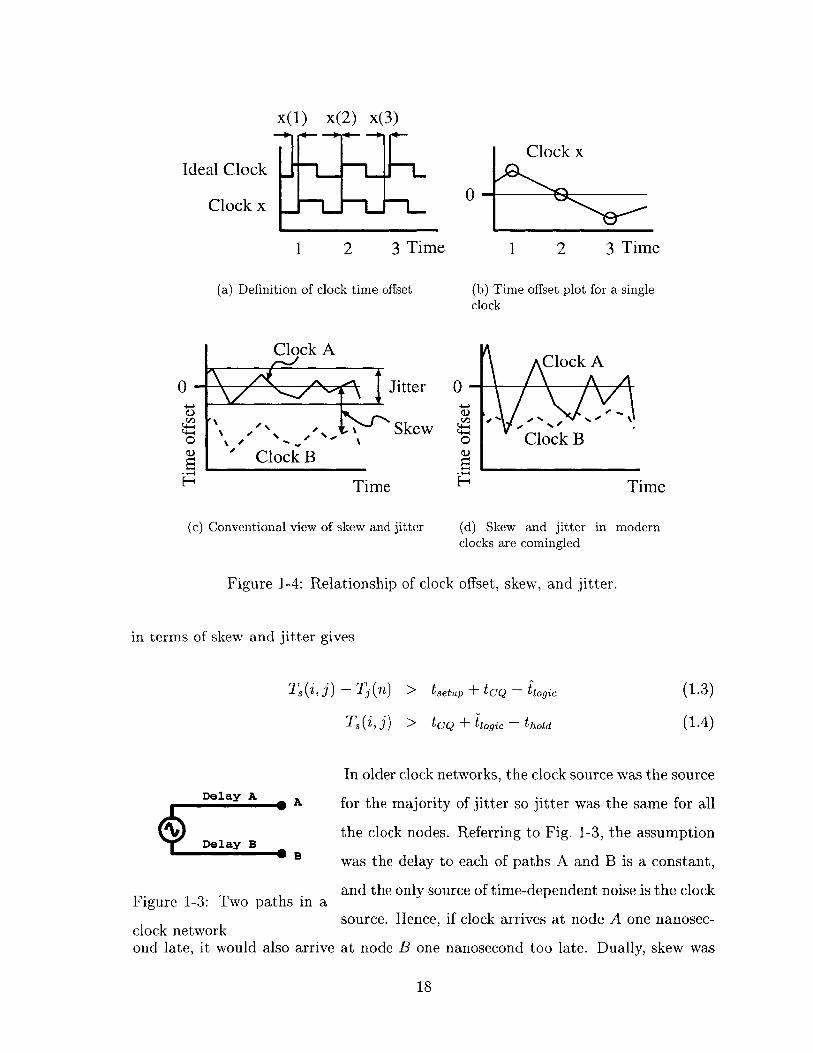
Traditionally, clock networks have been characterized in terms of skew, the spatial
variations in arrival times, or T,(i, j) T - Tj; and jitter, the temporal variation in
clock period at a node, Tj(n) = Ti,+- Ti,n - Tperiod. Rewriting Eq. 1.1 and Eq. 1.2
17
x(1) x(2) x(3)
Ideal Clock
Clock x LL
1 2 3 Time
(a) Definition of clock time offset
I Clock A
0-
4I)
o"~ dl Jitter
Skew
- Clock B
Time
(c) Conventional view of skew and jitter
0
Clock x
1 2 3 Time
(b) Time offset plot for a singleclock
0- NA Clock AA
Clock B
A
'NTime
(d) Skew and jitter in modernclocks are comingled
Figure 1-4: Relationship of clock offset, skew, and jitter.
in terms of skew and jitter gives
Ts (i, j) - T (n)
TS (i, A )
> tsetu + tCQ - tlogic
> tCQ + liogic - thold
Delay A A
DelayBB
Figure 1-3: Two paths in a
clock networkond late, it would also arrive
In older clock networks, the clock source was the source
for the majority of jitter so jitter was the same for all
the clock nodes. Referring to Fig. 1-3, the assumption
was the delay to each of paths A and B is a constant,
and the only source of time-dependent noise is the clock
source. Hence, if clock arrives at node A one nanosec-
at node B one nanosecond too late. Dually, skew was
18
(1.3)
(1.4)
A-

caused by static path-length mismatches to the clock loads, so skew was constant
from cycle to cycle. If on one clock cycle the clock at B lagged the clock at A by one
nanosecond, it would lag by one nanosecond at the next clock cycle as well. If we
plot the time offset from an ideal clock, defined in Fig. 1-4(a), vs. time for a single
clock, we'd expect to see something like Fig. 1-4(b). The traditional model suggests
that two on-chip clocks behave as shown in Fig. 1-4(c). In modern clock systems,
however, delay from the clock source to the loads dominates both static and dynamic
mismatches, so arrival times at different nodes are not necessarily correlated. If the
clock arrival time at node A is not correlated with the arrival time at node B, the
jitter at B need not match the jitter at A, and the skew between A and B becomes
time-varying, as shown in Fig. 1-4(d). This means that the skew and jitter terms
in Eq. 1.3 and Eq. 1.4 would have to be fully indexed for sample time and location.
In short, there is little reason to treat skew and jitter separately in modern clock
networks.
For this reason, this thesis uses "clock skew" and "clock uncertainty" interchange-
ably to mean the difference between the actual clock arrival time and the nominal
arrival time, whether the reference is established by spatially or temporally distinct
clock edge. Aside from avoiding semantic distinction between skew and jitter, this
usage allows us to consider skew and jitter contributions of individual clock paths,
rather than pairs of paths. (This is an exact clock network analog of analyzing half-
circuits in amplifier design.)
Just as there are distinctions between types of timing errors (hold vs. setup
violations), and between types of clock uncertainty (skew vs. jitter), there are sev-
eral divisions in the sources of clock uncertainty. First, errors can be divided into
systematic or random. Systematic errors are due to layout-dependent parameter
variations, length variations in the lines, load capacitance mismatches, etc. That is,
any variations that are the same from chip to chip. In principle, such errors could
be modeled and corrected at design time given sufficiently good simulators. Failing
that, systematic errors can be deduced from measurements over a set of chips, and the
design adjusted to compensate. Random errors are due to manufacturing variations,
19

inter-signal coupling (which is predictable but often too hard to model correctly),
thermal- and slow supply voltage-gradients, power-supply-noise-induced delay varia-
tions in buffers, and to some extent, thermal noise. It is impossible to eliminate some
sources of random clock uncertainty, but it is possible to model some of the skew and
jitter sources, and to design in a way that minimizes their effects.
Mismatch may also be characterized as static or time-varying. In practice, there
is a continuum between changes that are slower than the time constant of interest
and those that are faster. For example, temperature variations on a chip vary on a
millisecond time scale. A clock network tuned by a one-time calibration or trimming
would be vulnerable to time-varying mismatch due to varying thermal gradients. On
the other hand, to a feedback network with a bandwidth of several megahertz, thermal
changes appear essentially static. Note the caveat that time-varying signals can cause
static errors as long as they are periodic with the clock. For example, the clock net is
usually by far the largest single net on the chip, and simultaneous transitions on the
clock drivers induces noise on the power supply. However, this high speed effect does
not contribute to time-varying mismatch because it is the same on every clock cycle,
and hence affects each rising clock edge the same way. Of course, this power supply
glitch may still cause static mismatch if it is not the same throughout the chip.
Finally, random skew can be subdivided into spatially correlated and spatially
uncorrelated mismatch. (Note the similarity to static and time-varying mismatch,
which could be restated as temporally correlated and uncorrelated). Again, the dis-
tinction is not absolute. Different physical parameters will have different correlation
distances; hence it is possible for a single pair of wires to be correlated in one respect
but not in the other. Table 1.1 shows the categories and several examples of the
sources of each type of random mismatch.
correlated uncorrelatedstatic wafer-scale etching, polishing MOSFET channel doping
and lithography gradientstime-varying temperature and power-supply value-dependent load capaci-
gradients tance, inter-signal coupling
Table 1.1: Categorization and example sources of non-systematic mismatch
20

1.2 Thesis Scope
As argued in Chapter 2, signal delay across a microprocessor chip measured in clock
cycles has been increasing as technology scales to smaller feature sizes, and is now
comparable to one clock cycle. Because clock uncertainty scales with path delay,
relatively longer delays increase the fraction of clock uncertainty per clock cycle; this
trend could severely limit performance if not corrected. The overall goal of this thesis
was to examine clock performance at both the circuit and the architectural level to
find ways to design clocks in an environment where performance is limited by random
random physical mismatches and noise.
This thesis is split into three parts. The first part, Chapter 2, analyzes how
sources of skew and jitter affect different clock architectures. The nonintuitive result
is that a tree architecture is not well suited to systems where cycle time is shorter
than cross-chip path delay, and that distributed clock networks become increasingly
attractive.
This analysis leads into the second part, which proposes a novel clock network
composed of multiple synchronized phase-locked loops. Chapter 3 covers large- and
small-signal stability of the system. Undesirable large-signal stable (modelocked)
states dictate the transfer characteristic of the phase detectors; a matrix formula-
tion of the linearized system allows direct calculation of system poles for any desired
oscillator configuration. Chapter 4 deals with circuit implementation in CMOS, pre-
senting two implementations of the system- a 4 oscillator proof-of-concept 400MHz
network, and a 16-oscillator, 1.3GHz network network.
The last part of the thesis, Chapter 5, examines ways to measure performance
of a high-speed clock. As clock performance is optimized for fast operation, it be-
comes increasingly difficult to measure clock jitter. A flash time-to-digital converter
is presented that exploits parallelism to get precise time measurements with reso-
lution much smaller than a single gate delay. Unfortunately, an unrelated failure
precluded measurements on the 16-oscillator chip where the measurement system
was integrated, but the principle is shown to be valid on an independent test chip.
21

22

Chapter 2
Models of Clock Network Timing
Variations
Unpredictable parameter variations and noise are becoming dominant concerns for
clocks. Clock networks have traditionally been optimized for minimum design time
(gridded clocks) or power and wireability (trees). Process variations, on the other
hand, have been studied extensively in terms of matching limitations on analog cir-
cuits, and to some extent in individual clock architectures. This chapter considers
how clock uncertainty depends on both architecture and imposed mismatch.
2.1 Previous Work: Clocks
Consider first the taxonomy and evolution of clock networks. Note that a great deal
of work nominally about "clocking" has gone into finding the exact sequence of timing
signals needed to clock a microprocessor at the fastest possible speed [3, 4, 5, 6, 7, 8, 9],
and a number of CAD tools have been developed to find and verify such timing
schedules [10, 11, 12]. However, the analysis of what timing signals are needed is
independent of how the signals are distributed. Unpredictable variations are no more
tolerated in scheduled-skew designs than in ideally zero-skew designs. The remaining
discussion will assume that the optimal clocking schedule has already been determined
and that what remains is implementation.
23

2.1.1 Equipotential Clocking
Conceptually the simplest clocking strategy is to distribute a global clock to the
chip as a regular, though heavily loaded, signal line. This is known as equipotential
clocking because the implicit assumption is that resistance in the wires is negligible
and the entire net is always at a uniform voltage. For small nets with relatively
few clock loads and a slow clock, this works well. For large chips and fast clocks,
equipotential clocking has the advantage that most of the clock distribution network
can be designed independently of the logic.
In fact, there is some RC time constant (T) associated with the wires of such
a clock net. When T is small compared to the clock period, the RC delays are
unimportant. As feature sizes scale down, however, T increases and clock rates go up,
so the net no longer appears as a lumped capacitance and acts instead a lossy delay
line. Propagation delays along the clock net cause skew. Because T scales with the
size of the net, equipotential clocking can still be used for subsections of a chip [13],
and implicitly at the lowest level in hierarchical [14] and distributed [15, 16] designs.
The tour de force of equipotential clocking was the first DEC Alpha chip [17]
(Fig. 2-1(a)). In that design, a single, segmented buffer placed lengthwise in the
center of the die drives a grid made using two upper metal layers (i.e., the thickest
metal available, to lower T). The worst-case time difference between clock arrivals
was 200 picoseconds, and this was sufficient for a 200 MHz clock.
The next two versions, the 300 MHz Alpha and its strikingly similar 433 MHz
cousin, [18, 19] both used two drivers for the entire grid (Fig. 2-1(b)). Why? With
higher clock speeds, the RC delay from the center of the chip to the edges becomes
significant; the two drivers effectively both drive halves of the chip, so the delays are
shorter. The 600 MHz Alpha [2] (Fig. 2-1(c)) followed this trend: it has four top-level
buffers, because with the higher clock speeds and wire delays, ever smaller sections
of the chip can be modeled as equipotentials.
24

Wire Grid Drivers
-o---
Clock
(b) Two-driver grid
Driver
I I
Figure 2-1: Evolution of Alpha's grid based clock network. In all cases, large buffersdrive a regular mesh of metal2 and metal3 wires.
2.1.2 H-Trees and Generalized Trees
If it were possible to lay out the clock net so that all points where the clock is used
are equidistant from the clock driver, the wire delay would not cause skew. This idea
led to H-trees (Fig. 2-2) [20, 21, 14].
By symmetry, the distance from the center of
the net (the root of the tree), to each of the ends
(leaves), is the same. Therefore, regardless of T,
signals should arrive at the leaves at the same
time. The clock can then be distributed to a
smaller (approximately equipotential) net around
each leaf. The size of this equipotential region
around each leaf shrinks as the depth of the tree
increases, so deeper trees are needed for faster
clock speeds.
The maximum clock frequency is limited by
dispersion of pulses on the RC wires, so the basic
Leaf Leaf Leaf ...
Root
Leaf
Figure 2-2: Four level H-Tree.
Paths from the center to the
leaves are geometrically the same.
H-tree can be improved immediately by symmetrically inserting buffers along the
25
Drivers
I I
I I-- -- --- ----
Clock Metal Strap
(c) Windowpane grid
zlzI±Iz -
(a) One-driver grid

branches to regenerate the signal [21, 22, 15, 14]. Clock trees are insensitive to global
process and environmental variations; skew is still zero if the resistance of the wires
is higher than expected, say, or if the input threshold to all the buffers changes. Of
course, H-trees are affected by intra-die variations [23, 24]. Anything that causes
similar paths on the different parts of the chip to have different delays (e.g., local
line width variations, temperature gradients, varying threshold voltages, etc.) causes
skew.
H-trees are most useful when clocking regular arrays, because the leaves form a
regular grid. What can be done if the clock loading is not so geometrically regular?
The vital feature of H-trees is that the distance from the root to all the leaves is the
same. Finding a balanced tree for an arbitrary set of points is known as the zero-
skew tree problem. In general, finding a zero-skew tree with minimum total length
is exceptionally hard; however, a number of heuristic algorithms have been proposed
[25, 26, 27, 28, 29]. Closely related to the zero-skew problem is the bounded skew tree
problem, where a small amount of path difference is allowed to help minimize the
total wire length, and therefore minimize area and power dissipation [30].
All of these tree approaches are bottom-up
algorithms that start by connecting groups of
nodes into a tree and then merging trees until
Leaves only one net remains. They are distinguished
by exactly how they merge trees, behavior in
pathological cases, how the number of compu-Root tations scales with the number of clock loads,
Figure 2-3: Zero-skew balanced tree how they route around obstructions, etc. The
result is essentially the same, however: they all
produce an irregular clock tree that ties together a specified set of clock loads such
that the distance from the root to the leaves is approximately equal (Fig. 2-3). Most
modern processors use some version of such trees to distribute the clock [31, 32, 33, 34].
Those that do not use explicit trees still simulate and balance path delays from the
clock source to all the loads, so act essentially as generalized clock trees. There the
26

Global Clock
Delay Delay-_
-Compare+-
Figure 2-4: Digital active deskewing
matching is generally less precise, because the delay to the leaves, while nominally
identical, is composed of the delays of a variable number of gates and length of wire,
so even global variations in a particular parameter may cause skew.
2.1.3 Active Skew Management
One approach to measure and cancel out static skew involves splitting the H-tree
into two halves, measuring the relative offset between the two, and applying the
appropriate delay, as shown in Fig. 2-4 [35]. In this structure, the delays and control
signals are digital; this adds a measure of noise immunity, but increases the overhead
power and area. Further, the model does not scale well - there is explicit digital
control to guarantee that the delays do not both continue to increase. Splitting the
tree into more sections allows finer adjustment, but the control overhead increases
rapidly as well.
2.2 Previous Work: Variations
Because the goal of a clock network is to distribute an identical signal to multiple
locations, device and interconnect matching is important. Environmental variables,
such as supply voltage, switching activity and temperature depend on the design of
27
the chip, and hence are under the control of the designer. Conversely, processing
variables, including film thickness, lateral lengths, resistivity, etc., are defined by the
manufacturing process, and can be treated as imposed constraints [43]. This section
describes some of the approaches to modeling the constraints and their effects on
circuits.
2.2.1 Layout-Dependent Processing Variations
Some manufacturing process steps, most notably etching, chemical-mechanical pol-
ishing (CMP) and lithography, are influenced by topography on a chip. This layout-
depending processing causes systematic device and interconnect variations [43, 44, 45].
Modeling this variation falls into the realm of statistical metrology; see [46] for a re-
view. This systematic variation need not limit clock performance, however. Design
rules are evolving to ensure layout pattern uniformity. For some effects, it may be
feasible to add a spatially-varying fabrication mask offset, just as masks are made
by adjusting the drawn layout to compensate for lithography and etching biases.
As a last resort, clock performance can be measured and systematic offsets can be
compensated in the design.
2.2.2 Wafer-Scale and Random Physical Variations
Unlike systematic skew, skew caused by random physical variations is unavoidable.
For example, a dominant source of device mismatch over small areas is V variation
due to stochastic distribution of dopants; variation depends only on channel area
[47, 45, 48, 49]. Wafer-scale non-uniformity, while not truly random, varies from chip
to chip. For example, deposited thin films often have a radially-symmetric thickness
profile across a wafer. This results in slants in parameter properties across chips that
depend on position of the chip within a wafer, and hence cannot be compensated on
chip [43].
28

Voltage
Vth max
Vth min- - --
Time
tO t1 t2 t3
Figure 2-5: Clock skew caused by finite signal rise time. t1 - to and t3 - t 2 is skewdue to variable buffer threshold voltages. t3 - ti and t 2 - to is due to variable risetime. t3 - to shows the worst case combined effect.
2.2.3 Circuit Implications of Mismatch
Processing mismatch translates directly into loss of clock performance. For example,
variations in saturation current or buffer thresholds can both lead to variable clock
arrival times, as shown in Fig. 2-5 [21, 20]. Exact numbers are not easily available,
but one may assume that there could be 10% dynamic variation in VDD across a chip
(which affects the threshold and drive current) and another 5% variation in IDSS
between two distant, though nominally matched, buffers. That leads to an expected
clock skew of 2.5% of the total clock cycle from a single pair of gates! In the current
regime, where the clock skew budget is approximately 10% of the clock period, this
is quite substantial [22, 50, 51]. Attempts to increase the maximum clock speed by
increasing pipelining along an H-tree exacerbate this effect [52].
Because random variations cause substantial skew, there have been a number of
attempts to minimize mismatches at the circuit level. For example, it was noticed that
due to poor matching between nfets and pfets, signal paths which do not match the
nfets and pfets separately may add skew unnecessarily [53]. The canonical example is
shown in Fig. 2-6. On a rising input clock edge, gates N1, P2 and N3 are turned on
in the top chain and N4 and P5 in the bottom chain. Because nfets may be expected
to track nfets better than pfets, and vice versa, the lowest skew is achieved by sizing
29
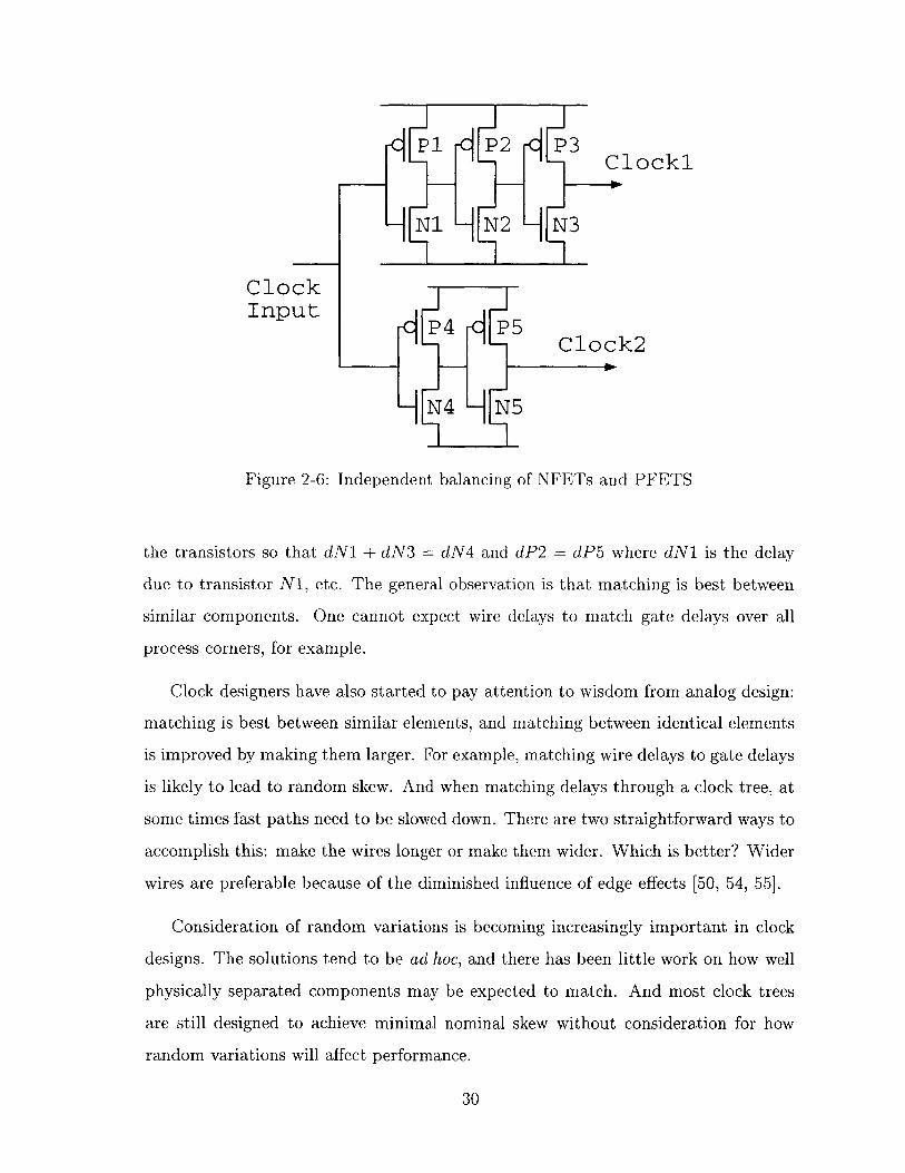
P1 P2 P3Clocki
N1 N2 N3
ClockInput
I n p u t 4 P 5 C l o c k 2
N4 N5
Figure 2-6: Independent balancing of NFETs and PFETS
the transistors so that dN1 + dN3 = dN4 and dP2 = dP5 where dN1 is the delay
due to transistor N1, etc. The general observation is that matching is best between
similar components. One cannot expect wire delays to match gate delays over all
process corners, for example.
Clock designers have also started to pay attention to wisdom from analog design:
matching is best between similar elements, and matching between identical elements
is improved by making them larger. For example, matching wire delays to gate delays
is likely to lead to random skew. And when matching delays through a clock tree, at
some times fast paths need to be slowed down. There are two straightforward ways to
accomplish this: make the wires longer or make them wider. Which is better? Wider
wires are preferable because of the diminished influence of edge effects [50, 54, 55].
Consideration of random variations is becoming increasingly important in clock
designs. The solutions tend to be ad hoc, and there has been little work on how well
physically separated components may be expected to match. And most clock trees
are still designed to achieve minimal nominal skew without consideration for how
random variations will affect performance.
30

2.2.4 Abstract Variation Models
At the other end of the extreme from the ad hoc physical models are the abstract
models for skew [15, 56, 42, 57]. The assumption in these models is that skew is caused
by uncorrelated, random variations in the clock distribution network. Unfortunately,
because they are so far removed from implementation, generic statistical models give
somewhat misleading results, for several reasons.
The first is that they are too optimistic about statistical independence of vari-
ations. For example, gates that are near each other are likely to match each other
more so than gates that are physically separated. This means that the sum of the
skews caused by gates in any signal path will have higher variance than would the
sum of skews caused by the same number of gates randomly selected from the chip.
Also, as has been pointed out, not all variations have the same weight in the final
skew: clock trees, for example, are much more sensitive to differences at the root of
the tree than at the leaves [56].
Ironically, the second weakness is that general statistical models can be too pes-
simistic as well. For example, an analysis of pulse width down a long line of buffers
suggests that the pulse-width follows a random walk [57]. Thus, it is argued, the
pulse might disappear entirely unless the clock period is sufficiently long. In fact, it
is not particularly hard to add feedback to ensure a 50% duty cycle, which effectively
limits the random walk. In this case and some others, circuit tricks can overcome
apparent stochastic barriers [15].
Fundamentally, the very generality that makes sweeping statistical statements
interesting is their weakness because such bounds do not take into account circuit
or architectural changes that affect network performance. Although they may place
bounds on clock performance, they are necessarily qualitative, and can neither suggest
circuit improvements nor take them into account.
31

2.3 Categories of Mismatch
All on-chip clock networks rely on device parameter matching. This is a crucial
difference between logic critical paths and clock networks: variation in critical path
delay can be overcome by speeding up the critical path so that the worst-case delay
meets timing constraints [58]. Time-dependency logic delay can be included directly
in the worst-case timing estimates: maximum delay is constrained by Eq. 1.3 and
minimum delay by Eq. 1.4. In contrast, because the clock network itself establishes
the timing, both too-slow and too fast clocks must be avoided. Physical variations
are often separated into separated into local and global contributions [59]. For the
purposes of clock distribution, time-varying mismatch must be considered explicitly
as jitter (and, if uncorrelated spatially, as contributing to skew). 1
Integrated circuit fabrication processes generally result in wafer-scale gradients
in line width (both metal and polysilicon), thin film thickness (metal wires, gate
oxide, interlayer dielectric) and doping concentration [43]. Manufacturing gradients
have been cited to explain distance-dependent mismatch in transistors [60]. These
variations significantly affect device and interconnect performance. In minimum-size
inverters, for example, Leff variation can lead to 9% delay mismatch [61] between
chips; in a different process 37% variation of ring oscillator speed was reported within
single dies [62]. Clocks depend on matching rather than absolute delays, and are
therefore insensitive to truly global parameter variations. We also make the optimistic
assumptions thatall systematic variations are compensated. This could be achieved
via modeling (i.e., statistical metrology), or simply testing finished chips if multiple
silicon revisions are to be made.
However, because clock networks span an entire chip, wafer-scale gradients are
noticeable. It is generally accepted that global effects can be ignored for distances
smaller than 100pm, but are noticeable for distances larger than 1mm [47, 60]. Global
environmental variations, specifically in temperature and DC supply voltage variation,
'There is a subtle asymmetry between temporal variation in logic and clock. Slack in Eq. 1.4 cannot be exploited to decrease clock cycle time, while any decrease in clock uncertainty directly lowersthe minimum clock period. For this reason, temporal variations of the clock are analyzed explicitly.
32

Figure 2-7: Example H-tree
Segment 1 2 3 4 5 6 7 AverageXi 0.1 0.3 0.5 0.5 0.5 0.4 0.25 .36
Table 2.1: Contributions to skew for an H-tree
are imposed by design rather than fabrication, but are otherwise similar in effect.
Temperature affects resistivity of the metal, channel mobility, and threshold voltages,
and supply voltage affects saturation currents and hence gate delay [63].
The distance between most nominally matched components of a clock distribution
network is comparable to chip size, which is typically 1cm or larger. Fig. 2-7 shows
an example H-tree, and the distances xi, normalized to chip size, between nominally
matched wire segments are tabulated in Table 2.1. Most of the distances are com-
parable to the size of a chip; hence, we may expect that the wafer-scale variations
are dominant and consider inter-chip mismatch data. Still, this brings up a messy
modeling issue.
Delay along a clock wire is a sum of small delays. The delay of each buffer-
33
x7
x5
x6
x4
X1x3
x2
wire-buffer segment contributes a small random component. If the segments are
strictly independent (e.g., uncorrelated threshold voltage variations), the variance
along the wire is the sum of individual variances, so the standard deviation of the
resulting offset increases as the square root of the length of the wire. Another model
is that the mismatch is due to a gradient of delays across a chip (perhaps from thin-
film deposition). Because the linear gradient is summed, the mismatch rises with the
square of the wire length. Finally, if the perturbations are each fixed-size or uniformly
distributed (e.g., a higher supply voltage for a section of the chip) , the worst-case
offset increases linearly with wire length.
Because gradients dominate over relatively long distances, it would probably be
most accurate to model short nearby wires with independent segments, long distant
wires in terms of gradients, and intermediate wires linearly. However, that obfuscates
the analysis unnecessarily; the key point is that short near wires match better than
long distant wires. For the sake of analysis, we will assume that uncertainty scales
linearly with delay with a mismatch coefficient a, as p(x) - p(0) . ap(O).
This argument can be extended to say that the variability in delay along a path
scales linearly with the delay along the path; that is, that there is a fixed percentage
error in on-chip path delay. We will use this assumption, although there is an impor-
tant caveat: a depends on the construction of the path. A Ins delay with a = 0.11
gives more skew (110ps) than a 1.lns delay with a = 0.09 (99ps). For this reason the
classic line-driver optimization may give suboptimal results if wire mismatch is not
the same as buffer mismatch. However, for the optimal combination, delay variability
will scale linearly with delay.
Of course, matching is not perfect for adjacent wires or devices either. Strong
sensitivity of threshold voltage and saturation current on L at short channels also
limits matching for minimum-size devices; typically saturation current has a 3% mis-
match for minimum devices, and matching down to 1% is straightforward in larger
devices. Local mismatch is an important limit for phase detector offset in PLL and
DLL systems.
Time-varying effects include capacitive and inductive coupling between signal and
34
clock lines and signal-dependent capacitance. Careful layout can minimize the ca-
pacitance between signal lines likely to switch near clock edges and clock wires, but
signal coupling is still important because it can be a significant source of jitter. We
will assume that up to 5% of the capacitance of any wire may transition during the
time a clock edge propagates.
Temperature changes on a chip are generally many orders of magnitude slower
than the clock speed, and are therefore reasonably treated as static gradients. On
the other hand, supply voltage can change within a single clock cycle in response
to changing load current. For this reason, temporal correlation is important when
matching elements that depend on supply voltage. An example where this is signifi-
cant is described in Section 2.4.4.
2.4 Clock Architecture Comparison
While a number of authors have considered the impact of variations on clock perfor-
mance, most assume tree distribution [52, 41, 63]. This section establishes a common
metric and compares several clock architectures.
2.4.1 Clock metric
The three categories of mismatches listed above cover what is needed for a first-order
comparison of clock networks. For normalization, each is scaled to distribute a 1 GHz
clock to a total of 200pF load capacitance over a 2cm chip in a standard 0.25pm
CMOS process. A clock wire in a TSMC 0.25pm CMOS process would be 1pm wide,
have a resistance of about 0.07Q/pm, and a capacitance of .lfF/pm.
It would be convenient to choose a single parameter to characterize clock networks.
As discussed earlier, skew and jitter are in general functions of both position and
time. It is appropriate to consider the worst case clock uncertainty over time, but
meaningless to look at worst case across a chip: in all practical cases a signal that
takes longer than a clock cycle to propagate would be pipelined, and hence re-clocked.
Hence, clock uncertainty between points on a chip further apart than one clock cycle is
35

.05C
Figure 2-8: Schematic model of capacitive coupling
irrelevant. For this reason, the metric for clock quality will be taken to be worst-case
clock mismatch over a distance corresponding to signal propagation distance during
one half of a clock cycle.
2.4.2 Tree
Propagation delay along an H-tree can be split into delay from the root to the leaves,
and delay from the leaves to a sub-block or tile. Delays to loads from a leaf are
generally not matched, so the entire delay in a sub-block adds directly to total skew;
this is sometimes called internal clock skew [14, 63]. The point of an H-tree, however,
is to match delays from the root to the leaves, so those delays are nominally matched,
and only variations contribute to skew. Consider a 8-level H-tree (i.e., one with
28 = 256 leaves). Assuming equal-sized buffers along the tree, these buffers would be
placed at intervals of perhaps 2mm, for a total of 10 segments.
Delay along the tree in this example is simulated to be 0.86ns. Assuming a = 0.1,
skew caused by gradient mismatch is 0.86ns x 0.1 = 86ps. Internal skew (Si) is no
larger than 0.07Q x 625pm x 0.2pF ~ 9ps.
Capacitive coupling adds a time-varying offset. Fig. 2-8 shows the schematic
model used to test the effect of capacitive coupling. The effect may be estimated by
adjusting the effective line capacitance for the Miller-multiplied coupling capacitance.
In the current example, the line capacitance is 200fF, the output capacitance of the
driving buffer is 34fF, and the input capacitance to the receiving buffer is 77fF. A
signal making a transition in the same direction as the clock lowers the effective wire
36

capacitance by 5% (given the assumptions above), so the delay should decrease by
.05x200 ; 3%. Conversely, a signal transitioning in the opposite direction will slow200+ 111
down the clock by the same 3%, so the total would be up to 6% variation. (Simulation
indicates the total variation is 5%). This component of uncertainty - skew if the
interference recurs on every clock cycle, jitter if it is inconsistent - also scales with
the total delay along the tree, and so adds a worst-case 45ps to clock uncertainty.
To sum up, a clock distributed by a tree as described above will have skew of 140
picoseconds, or 14% of the clock cycle; this is in line with industrial results given the
speed and assumptions about the process.
Generalization
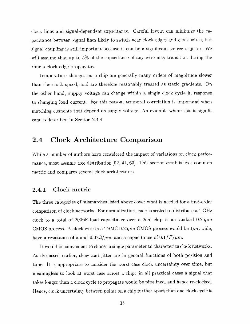
We can generalize from this example to other trees. Fig. 2-9(a) shows how the two
components of skew change with the depth of the tree, n. (The tree of this example
had n = 8.) As argued above, both mismatch and coupling cause skew proportional
to wire length L from root to leaves of the tree; in units of chip size, L = 1 - (1/2)n/2.
Internal skew scales inversely with the area2 of the resulting patch, so Si oc 2-.
The other key parameter is power. Power scales linearly with switched capaci-
tance, so the clock distribution power (excluding the load) scales as 2n/2. Fig. 2-9(b)
combines the results into a plot of the fundamental clock network tradeoff between
power and performance.
Scaling
Note, however, that a clock tree does not scale well with process technology. As
chip dimensions shrink, wire delay (T) is, at best, constant. Total chip size is also
nearly constant. However, clock speeds increase as the gate delay decreases. Delay
along the clock net also speeds up, but not by the same factor. Along an optimally
buffered line, the ratio of gate delay (d) to T is constant, so as d falls, the distance
between buffers decreases. Wire delay is proportional to the square of the wire length
2Strictly speaking, it scales with length squared, but that is equivalent to area for non-pathologicalpatches
37
10 4 100-x- area-scaled skew 0-&- length-scaled skew -2
U-- total 0
2US10 2 10 - -
co 0
C N
10 1s -210 E 100 0
0
10 10 10 102 10 10depth of tree skew, ps
(a) Skew components in a tree vs. tree depth (b) Power vs. skew for a clock tree
Figure 2-9: Clock tree tradeoffs
between buffers (1). Hence 1 cx Vd. The total number of segments is proportional to
1/1, so the total delay along a tree is proportional to d/Vdi = v /d. Since the clock
speed is directly proportional to d, skew as a fraction of the clock period will grow
as 1/v d as gate delay falls. In other words, without a dramatic redesign or process
improvements, a 4GHz clock tree would have unpredictable clock skew of 30% of a
clock period, and a 16GHz clock would have to budget over half of the clock period
for skew and jitter margin.
Note that as clock speed increases, signal delay across a chip exceeds a single
clock cycle. In the example above, a 2cm-long wire has a delay of 0.86ns with 1GHz
clocks. Scaling to 4GHz, the same wire (with optimal buffering) will have a delay of
approximately 0.43ns, compared to a clock period of 0.25ns. Given the metric defined
in Section 2.4.1, therefore, there is no reason to minimize global skew at all. In a tree,
however, the worst-case skew occurs between nearest neighbors, so tree distribution
cannot take advantage of the relaxed global constraints. This is the fundamental
reason why trees become less attractive at high clock speeds.
38

Global Clock
Figure 2-10: Grid distribution block schematic
2.4.3 Grid
A pure grid network would have a single, central driver for the entire chip and a mesh
of clock wires. Skew would be simply the wire delay across the chip, just as it is the
wire delay in a patch for each leaf of a tree. In the limiting case, a clock plane with a
central driver would give skew of .07Q/pm x .lf F/um x (104pm) 2 = 0.7ns.3 Clearly,
a single driver will not give adequate performance, so modern grids are H-tree-grid
hybrids: a short H-tree distributes clock to a few (4 or 16, for example) buffers around
a chip, and those buffers drive a clock grid in parallel, as shown in Fig. 2-10. The
final patches are larger than those typical of trees, but the grid helps eliminate skew
caused by the tree distribution by shorting together outputs of multiple buffers.
Take as an example system a 4 level (24 = 16 node) clock tree where the final
buffers drive a global grid. Following the example of the previous section, such a tree
would have 7 2mm-long segments and an expected clock uncertainty of 70ps. Delay
across each region, assuming a lumped model with minimum-width wires, would give
a skew of 2.5mm x 70Q/mm x 6.25pF ~ 1ns. Because this skew is dominated by
wire resistance and load capacitance, it can be reduced by increasing the width of the
wires at the cost of increased power. At the point where the capacitance of the wires
3Scaling this value down to the size of the first Alpha gives skew ~ 200ps, which was reportedfor that chip.
39

Figure 2-11: Model circuit for shorted grid drivers.
equals the load capacitance there is one clock wire every 200pm, and the expected
wire skew is 89ps, (85ps simulated).
Furthermore, shorting the buffers together helps drive down some of the uncer-
tainty at the cost of increased short-circuit power during switching and somewhat
slower edge rates. A simple circuit model for a grid driven from multiple points is
shown in Fig. 2-11. Simulations with an 70 picosecond skew on buffer inputs show
a total skew of 145ps, of which 55ps is due to the input skew. It is possible to keep
driving this lower by increasing wire width; however, the benefits of wider wires get
incrementally smaller as the wire capacitance comes to dominate the total. Doubling
the wire width again, for example, lowers total skew to 110ps, of which 34ps is due
to the input.
The drawback, of course, is the power dissipation. The extra wiring needed to get
110ps skew down added 25pF of capacitance per buffer, while the clock load per buffer
is only 12.5pf. Still, grid distribution is used because much of the skew is predictable
and, unlike with H-trees, the clock design is largely independent of floorplanning.
40

100
00o 075 10
0
101N
S10'
0CL10-3
101 102 103
skew, ps
Figure 2-12: Power vs. skew for a grid.
Generalization
The primary parameter for a gridded clock is the capacitance of the grid (C); that
sets both the power dissipation (P oc C) and the wire skew. Si is proportional to
1 + CL/C where CL is the load capacitance and C the grid capacitance. Mismatch-
induced skew is shorted out by lower-resistance wires, so that component of skew falls
as 1/CL. A plot of simulated power dissipation vs. skew, corresponding to Fig. 2-9(b)
is shown in Fig. 2-12.
Scaling
Grid distributions depend only on wire delays. As mentioned above, wire delays tend
not to improve with process technology scaling. As the skew budget decreases with
rising clock speed, a grid clock must either increase capacitance or subdivide the chip
further with a deeper initial clock tree. In the example above, the initial tree itself
does not add significant power, so an obvious scaling strategy would be to simply
make larger trees to minimize Si.
As long as delay variations in the initial tree are comparable to rise time, deeper
trees and smaller Si will improve performance. However, rise time scales linearly
with d, so by the same reasoning as as applied to the tree scaling arguments, skew
41

as a fraction of rise time will increase with 1/vd as gate delay falls. When the tree
skew exceeds rise time short circuit power dissipation increases rapidly, and the clock
edges begin to show an unacceptable kink. Fig. 2-13 shows simulated edge shapes
with increasing input skew for a grid driven from a 4-level tree with skews from 0 to
200ps, and Fig. 2-14 shows the corresponding short circuit power dissipation.
DCWAO:v) y-
D0: V(xbs1) -
3.2
3
2.8
2.6 -
2.4
2.2
1.8
1.6
1.4 -
1.2
1T
800m -
400m
200m
0
-20Cm -
3.6n 3.65n 3.7n 3.75n 3.8n 3.85n 3.9n 3.95nTime (fin) (TIME)
4n 4.05n 4.1n 4.16n 4.2n 4.25n
Figure 2-13: Simulated edge in a grid with skew to the drivers.
2.4.4 Active Feedback
As is evident from the sections above, an increasing share of skew comes from the
initial long-distance distribution of a clock to relatively small loads. A delay-locked
loop (DLL) could be adapted to measure and cancel out wire variations. One possible
implementation is shown in Fig. 2-15, where a DLL is used to implement a single wire
with low effective delay. The intuition is that the delays are adjusted symmetrically
until the round trip time from the source to the load and back is a known multiple
of a clock period; (in line with the examples so far, assume the round trip time is
42
edge shape with input skew

0.5
0 0.4-
> 0.3
0c_00.2a)N
E0.10
0 50 100 150 200input skew, ps
Figure 2-14: Short circuit power in a grid vs. input tree skew.
Source D/2 W1 b2 w2 bw13 w3 b4
Load
b8 w7 b7 w6 b6< w5 b5
Figure 2-15: Low-skew wire with DLL
2ns, which is 2 clock periods). Then by symmetry, the signal arrives at the load
with a 1 period clock delay, which means it has effectively 0 delay for clock signals.
Unfortunately, this intuition is misleading.
Despite the apparent symmetry, there is little reason for the forward path to
match the reverse path in this connection for two main reasons. First, the nominally
matched buffers are physically separated. In Fig. 2-15, b1 should match b7 , although
it would be physically near b8 . b, isn't as far away from its matched pair as it might be
in a tree, but it will still typically be millimeters away. Second, there is no temporal
correlation. The clock signal passes w, at a different time than it passes w7 , so
any time-dependent variations, including those due to power supply and capacitive
coupling, do not match. Taking the results from Section 2.4.2, the effective skew for a
1cm-long DLL wire would be ~ 90ps, which is only a 30% improvement over a simple
43

Global Clock
Figure 2-16: Matching tree leaves with a DLL
wire, and that does not count offset in the comparison of the two edges or mismatches
in the delay cells.
Another approach, more like a traditional DLL, is shown in Fig. 2-16. The global
clock is distributed to two half H-trees, a phase comparison is done at the leaves, and
a variable delay is adjusted to align the clocks. The technique is meant to balance
delays along path 1 (di) and path 4 (d4 ) in this example. Note, however, that while
nodes A and B may be matched, nodes C and D are not; the mismatch between
nodes C and D (mcD) is (d + d3) - (d4 + d6) . The loop drives d, + d2 = d4 d5 SO5
mcD (d- -2)- (d- -), which is somewhat smaller than it would be without the
DLL (in which case moD =(d, - d4 ) + (d3- d6)) because W2 and w5 are both closer
together, and shorter, than d, and 4.
An immediate generalization would be to break up the trees further, have two
more comparators, and variable delay elements, as in Fig. 2-17. (Note the difference
between Fig. 2-17 and Fig. 2-18. The latter generalization requires matching between
delay elements D2 and D5, and between D 3 and D6; the former does not require that
the delay elements match at all.) Because delays to the leaves are controlled by DLLs,
the top-level tree structure is no longer necessary; Fig. 2-19 shows a DLL distribution
where each DLL drives a local tree. Static delay variations of nearest neighbors are
cancelled out by the DLL to within the precision of the matching of the comparators.
44

Global Clock
1 4A U B
D 2 5 D
DC
1 Cj
3 6
C D
Figure 2-17: Matching tree leaves with two DLLs
Global Clock
7Compare 7 E 4
D2 D5
D3D6 8-r F
CompareI I
Figure 2-18: Matching tree leaves with a two DLLs which requires delay cell matching
45

Global Clock
Compare
Compare
Delay Dela
Compare Compare
Delay Delay
A B
Figure 2-19: DLL architecture
Dynamic variations, due to supply noise or signal coupling, however, persist; two
1cm-long paths with active DLL matching will have a relative jitter of approximately
50ps (all of it time-varying), and skew from mismatch in the phase detectors, and
some mismatch from distribution along local trees. A typical phase detector has a
delay equal to 2 inverters, and its two halves are physically close together, so skew
is expected to be approximately 2 x 5% x d ~ 10ps. As drawn, the maximum skew
in the network is not between two paths connected with a DLL; rather, the skew
between A and B is the sum of the skews through three DLL's (10ps each) and four
local trees (25ps each). Total clock uncertainty between A and B, then, is 180ps and
the scaling is even worse because the effective distance between two nearby points
grows rapidly as the number of DLLs increases. A much better result can be obtained
by using DLLs that take multiple reference inputs, and adjust output phase to be
aligned exactly between the two inputs. The network can then be redrawn somewhat
more symmetrically, as Fig. 2-20. (For clarity, the local tree was not drawn, and the
connections to the comparators are abstracted.)
Optimization of the number of the number of tiles is straightforward. As argued
previously, internal skew scales with tile area, so as the number of tiles increases,
internal skew falls. However, every boundary between tiles introduces some skew
46

Global Clock
............................. ........ ......
Delay o a e Delay... ...... ...... . ..................................... ................. ............... ....... .......... .......
............................. ............ .. . . . . . . . . . . . . . . ...........I ...................... ... ...................... .............
.......................Compare Compare........................... ............... ..... ......... .......
....... ..................................... ............................... ............................................................. ....... ...Delay Compare Delay
Figure 2-20: Multi-input delay cell DLL architecture
100
C.
-. )
o
80-
60
40
20-
0
)
1 4 9 16 25 36 49 64number of tiles
Figure 2-21: Tile number optimization
because of mismatch in the phase detector. Hence, as the number of tiles increases, the
number of boundaries increases. Fig. 2-21 shows the optimization curves calculated
for this clock metric.
One inherent weakness of DLL networks is that DLLs are inherently sensitive
to input jitter. A phase-locked loop, (PLL), though somewhat more complicated in
implementation, filters out noise on the inputs. PLLs and DLLs are nearly identical
structures in isolation. Each has a variable delay element as a core, represented in
Fig. 2-22(a). An input signal with phase 0 is delayed by some time A and output with
phase q. In both the DLL and PLL cases (Fig. 2-22(b) and Fig. 2-22(c)), A = - 0.
The only difference is where the input signal comes from. If the input to the block is
47
-x- area-scaled skew-e- boundary skew_g_- total

ApA
A t
(a) Variable delay block (b) Delay-locked loop (c) Phase-locked loop
Figure 2-22: A variable delay element and phase comparator can be configured intoa DLL or a PLL.
0, the system acts as a PLL; if it is 0, a DLL. The noise and stability implications of
the feedback will be considered in the next chapter.
Scaling
As in other clock networks, faster clocks require a more finely-grained architecture.
Jitter in a DLL network will rise in exactly the same way as it increases in clock
trees, and for the same reasons. Skew scales linearly with d because it is comprised
of comparator mismatches and delays across each leaf-patch. Note, however, that
in a PLL the noise can be expected to scale with d; a PLL network like the one in
Fig. 2-20 would have total clock uncertainty that is a constant fraction of the clock
period.
48

Chapter 3
Synchronization and Stability
The purpose of an on-chip clock is to synchronize computation. Distributed networks
make explicit this synchronization. Chapter 2 argues that the performance of dis-
tributed clock networks scales favorably with clock speed (or at least does not scale
as poorly as do clock trees). This chapter gives some background on synchronization
architectures and then considers the synchronization of multiple oscillators.
3.1 Previous Work: Synchronization
The are two main synchronization schemes. In the first method, handshaking guar-
antees that computation proceeds in the correct order, although independent process
are not synchronized in any way. In the latter method, a global clock is used to syn-
chronize data, but the generation of the global clock is split among multiple blocks
that must align their respective clocks.
3.1.1 Local Data Synchronization
The earliest distributed networks dealt with synchronization of data explicitly, rather
than of multiple clocks. The archetypical example of this is large processor arrays.
It has been suggested that the computational density available in modern VLSI be
used to build large arrays of simple processors which communicate only with nearest
49

neighbors [21, 20, 15, 16]. Since skew is only relevant between communicating proces-
sors [7], trees do not seem well suited to the problem: there is no reason to eliminate
global skew as long as the clock skew between neighboring processors is low. This can
be accomplished by having each processor synchronize directly with its peers.
So-called self-timed systems use handshaking between the blocks for synchroniza-
tion [21, 41]. Each communication path between two blocks is accompanied by extra
signals that implement some manner of flow control. For example:
1. The processor sending data puts the data on the wire and asserts a Data Ready
signal.
2. The receiving processor reads the data and then asserts a Data Accepted
signal.
3. Data Ready is unasserted.
4. Data Accepted is unasserted.
Because no global synchronization is needed, self-timed systems are an example
of an asynchronous system. Such systems have several advantages over globally syn-
chronized systems: there is no global clock to propagate, and each block can work at
its actual speed rather than the global worst-case clock speed [21]. However, there
are several significant drawbacks: there is circuit overhead in generating the local
synchronization signals; the designs are notoriously hard to analyze and test; and
often the system operates at the worst-case time anyway, because computation is
always limited by the latest input [15, 41, 42]. The approach suggested by El-Amawy
[16] avoids some of these problems by having a system that looks fully synchronous,
albeit with some local clock skew. However, there is still no global synchronization,
and communication is only allowed between neighboring processors. Despite these
drawbacks, asynchronous systems are an alternative to global clocking, and may be-
come more prevalent if the prospects of very high speed clock distribution are not
improved.
50

Clock Signal
Node 1
12 Node 2
Node 3
Node 4
Time
Figure 3-1: Mode-locking example
3.1.2 Local Clock Synchronization
The proposed clock distribution architecture is organized as a synchronous array.
That is, clocks are generated at multiple places over the chip and controlled to have
the same phase and frequency. This approach has not been used in integrated clocks,
but it has been proposed for parallel computers, and some of the issues are similar
[40]. Pratt and Nguyen suggest constructing a clock for a parallel computer from
synchronized, voltage-controlled quartz crystal oscillators. Phase detectors and inte-
grators generate phase error signals, and these are used to pull the crystals to the
same phase and frequency.
While the desired, phase-locked configuration can be proven stable, it is possible
that some arrangement of unequal clock phases is also stable on a given network;
this effect is known as mode-locking. In the simplest example, a system consisting of
four nodes is stable although the phases are not equal, as shown in Fig. 3-1. Each
node sees one neighbor leading and one lagging, and therefore doesn't adjust. The
authors show that mode-locking can be avoided in a regular mesh with nonlinear
phase detectors, which they implement as balanced XOR gates.
This architecture is inconvenient for on-chip clock distribution for several rea-
sons. First, modern microprocessors are not organized as regular structures inter-
nally; memory caches and ALUs have vastly different clocking needs. Therefore it
will be necessary to remove the constraint that the clock nodes form a regular array.
51

Second, this method depends on having relatively noise-free, well-matched crystal os-
cillators, but such oscillators are not available on chip, and what is available has much
worse short-term stability. Therefore, the phase comparators and stabilization net-
work must be completely redesigned to compensate for the noisier oscillators. Third,
they assume that wire delays between nodes are negligible; on an IC, these delays are
the very heart of the problem.
3.2 Proposed Clock Architecture
The proposed distributed clock network is an array of synchronized PLL. Independent
oscillators generate the clock signal at multiple points ("nodes") across a chip; each
oscillator distributes the clock to only to a small section of the chip ("tile") (Fig. 3-2).
Phase detectors (PD) at the boundaries between tiles produce error signals that are
summed by an amplifier in each tile and used to adjust the frequency of the node
oscillator. In general, the network need not be square or regular.
With locally generated clocks, there are no chip-length clock lines to couple in jit-
ter; skew is introduced only by asymmetries in phase detectors instead of mismatches
in physically separated buffers; and the clock is regenerated at each node, so high
frequency jitter does not accumulate with distance from the clock source. Unlike
earlier work on multiple clock domains which suggested the use of multiple indepen-
dent clocks, this approach produces a single fully synchronized clock. The rest of this
chapter examines small and large signal stability of a distributed phase-locked loop.
3.3 Small Signal
In a multiple-oscillator PLL large- and small-signal behavior are interrelated. In
normal operation, the oscillators are phase-locked, and jitter depends on the network
response to noise. Because startup is expected to take a negligibly small fraction of
time, the connection of the oscillators is optimized for small-signal behavior rather
than to make initial acquisition more efficient. The linearized small signal behavior,
52

valid when the oscillators are nearly in phase, is analyzed first.
3.3.1 General Derivation
A traditional phase-locked loop (PLL) consists of three components: a voltage con-
trolled oscillator (VCO), a phase detector (PD), and a low-pass loop filter, connected
as shown in Fig. 3-3. In a digital application like clock generation, the output of the
oscillator is a square wave, and the phase detector generates a signal that on average
is related to the difference in phase between two square waves. Clearly, both the
oscillator and the phase detector are nonlinear in a strict sense. However, there is an
approximately linear relationship between the input voltage of the oscillator and the
phase of the output square wave. The relationship between the input phase difference
and averaged output of the phase detector is also linear. Hence, the system can be
modeled as a linear feedback system Fig. 3-4. The system as drawn in Fig. 3-4 is
described by:
aHi(s)- (u - ) (3.1)
= aH(s)/(s + aH(s)) u (3.2)
where u is the input phase. The poles of the system are the solutions of
aH(s) + 1 = 0 (3.3)
Substituting H(s) = (s + z)/s into Eq. 3.3 gives
a(s + z) + S2 = 0 (3.4)
which is a familiar result for a simple phase locked loop.
Exactly the same analysis applies to a network of coupled oscillators. Consider a
set of interlocked PLLs, as shown in Fig. 3-5.
The network can be modeled as a multivariable linear system; in fact, the block
53

Chip Boundary
ile Boundary
Phase
Detector
Loop Filter&vco& VCOj
Figure 3-2: Distributed clocking network
Reference timer-CLooptput
PDFilter Otu
Figure 3-3: Standard phase-locked loop.
Loop Filter VCOPD
Reference Output
s s
............ (voltage) ---.--..
(phase)
Figure 3-4: Linear system model of a standard phase-locked loop.
54

Reference L r F L r VCOPD ---- 1 FitrPD ----- 0 Fle
Loop VC0 Loop VCOPDFilter PDFilter
Figure 3-5: Multi-oscillator phase-locked loop
PD Loop Filter VCO
Reference N Outputj 21- A -- *, A2 *h ( s) N a
N
Figure 3-6: Linear system model of a multi-oscillator phase-locked loop
diagram (Fig. 3-6) is essentially identical to the one for a single oscillator system,
except that the connections between blocks are vectors instead of individual signals,
and the gains and transfer functions are matrices instead of scalars. This means that
the phase detector becomes a matrix A1 of size N(N + 1)/2 x N instead of a single
subtraction, and the loop filter becomes A2, a corresponding N x N(N+ 1)/2 matrix.
G = A2A1 is an intuitively meaningful N x N matrix. The network of oscillators
is similar to a lumped circuit C with a node for each oscillator and a branch for
each connection between pairs of oscillators. Node voltages in C represent oscillator
phase, and branch currents represent the error signals on the output of the phase
detector. G is the conductance matrix for C with unity conductance branches. G for
a 4 oscillator network is shown in Eq. 3.5. Each off-diagonal entry gij is -1 if there is
a phase detector between node i and node j; gij is the number of detectors attached
55

to node i.
3 -1 -1 0 '
-1 2 0 -1G = (3.5)
-1 0 2 -1
0 -1 -1 2
DC gain in the loop can be lumped into a3 .
Recasting Eq. 3.1 in matrix form gives Eq. 3.6,
4b = [sI + a3A 2Aih(s)]-' h(s)a3A 2U (3.6)
where u is now the phase error input to each phase comparator. In other words, u(1)
is the reference phase, and u(2) ... u(n) are the noise contributions from interconnect
and phase detector mismatch.
3.3.2 Examples
Matrix A1 is determined by the geometry of the tiles, and hence will constrained by
the placement of clock loads, which for this problem is fixed. Assuming the simplest
possible phase-locked loop, h(s) = (s + z)/s. This leaves A2 , a3 , and z as design
variables.
There are still far too many choices to find the general optimum, but a few exam-
ples may help guide the search.
Single oscillator
The reference design is a single-oscillator phase-locked loop. Stability constraints of
a single oscillator PLL may be derived directly from Eq. 3.3; however, it is more
common and more intuitive to analyze the loop gain, ah(s)/s. Magnitude and phase
Bode plots of the loop gain are shown in Fig. 3-7. Note that because of sampling at
the phase detector, the continuous time approximation is only valid for frequencies
much lower than the oscillator frequency. The Bode plots below add multiple parasitic
56

poles at the clock frequency we, to model the phase effects of the sampling. For the
0 -90
00
0000
-18000
Z 0io O
z (00 ) C log (P) log(O))
(a) Loop gain magnitude (b) Loop gain phase
Figure 3-7: PLL loop gain Bode plots
PLL to be stable and sufficiently damped, the phase must be above -135 when the
loop gain is at OdB. This means that the unity-gain frequency, wo, should be much
lower than w, and that the zero, z, should be much lower than wo. The location of
the dominant pole is not critical to the stability.
For a typical 1GHz oscillator, a = co ~~ 330MHz, consistent with the constraint
wo < we. In turn, this puts an upper limit of 50MHz on z. Fig. 3-8 shows the root
locus for this PLL over a gain error from -50% to 100%.
One dimensional array
A one-dimensional array of oscillators with phase detectors between neighbors is the
first generalization of a single PLL. In a perfectly asymmetrical array (call this system
S1 ), the output of PLL i is the input to PLL i+1, as shown in Fig. 3-9. S is described
by
1 0 0 0 1 0 0 0
-1 1 0 0 0 10 0A1 = A 2 ,1 (3.7)
0 -1 1 0 0 0 1 0
0 0 -1 1 0 0 0 1
57

x 10 7
6 -
4 -x
u) 2- x-<C x< n 0 K< - X - -. . . - X > 0 0 x x. .. .. O -Mx
EX
-4 -
-6
-1.5 -1 -0.5Real Axis x 108
Figure 3-8: Root locus for single-oscillator PLL with gain error
N
Ref
P
Figure 3-9: Asymmetrical one-dimensional PLL array
58

This system has multiple poles at the same place where a single-oscillator PLL has
single poles.
On the other hand, in a perfectly symmetrical array (call it S2 ), the input to each
oscillator i is the phase of oscillators i - 1 and i + 1 (Fig. 3-10). The A1 matrix is the
N
Ref
P
Figure 3-10: Symmetrical one-dimensional PLL array
same because the physical arrangement of nodes is identical, but A2 changes:
1 -1 0 0
0 1 -1 0A2 ,2 = (3.8)
0 0 1 -1
0 0 0 1
To achieve the same phase margin in S2 as in S1, it is necessary to lower the gain a 3.
This can be shown with a geometrical argument: in S2, when the phase of oscillator
i changes by A0q, the change is measured at two phase detectors, so oscillator i feels
twice the feedback that it would have felt in S1 , and at the same time, oscillators
i - 1 and i+ 1 both adjust in the opposite direction, giving 4 times the effective gain.
Hence, the gain must be decreased by a factor of approximately 4. Mathematically,
the largest eigenvalues of A 2 ,1 A 1 is 1, but the largest eigenvalue of A 2 ,2 A1 is 3.5.
Poles of the symmetrical system, solved via Eq. 3.61 are plotted in Fig. 3-11. The
'While it is possible to use Eq. 3.6 directly, it is often more convenient to take advantage of the
59

3
2- x
1 --
xOK X x x xI
x
-1--
-2 x
-3-6 -4 -2 0
Figure 3-11: Root locus for a one-dimensional array of PLLs.
60

key difference between Si and S2 is the systems' response to noise. In both cases,
noise at frequencies higher than the unity gain frequency wO are attenuated. For
frequencies much lower than wo, the response can be calculated via Eq. 3.6. Fig. 3-
12 shows a Bode plot of noise at node P in response to a noise source at node N.
Noise performance of Si is much worse for intermediate frequencies because there is
Noise
0- ------ ------
-10-
-20- symmetrical
-30 - - - asymmetrical
-40.
Freq0.001 0.01 0.1 1
Figure 3-12: Comparison of noise responses for symmetrical and asymmetrical net-works
no feedback so errors propagate forever. In S2, the feedback limits the influence of
preceding stages, and this in turn attenuates noise. For this reason, networks with
feedback are preferred, despite the more complicated stability calculation.
Two dimensional array
A two dimensional array is analyzed exactly the same was as is a one-dimensional
array, except that the gain has to decrease by another factor of two because the center
oscillators see four neighbors rather than two. A 16-element array in a 4 x 4 grid is
simple form of h(s), and rewrite the zero-input state equations thus:
S ' 0 I 0 10#' = 0 0 I 0' (3.9)
$"-Gz -G -pI ) "1
61

implemented in this thesis. Its G matrix and poles are shown below.
1 0 0 1 0 0 0 0 0 0 0 0 0 0 0)
1 -3 1 0 0 1 0 0 0 0 0 0 0 0 0 0
0 1 -3 1 0 0 1 0 0 0 0 0 0 0 0 0
0 0 1 -2 0 0 0 1 0 0 0 0 0 0 0 0
1 0 0 0 -3 1 0 0 1 0 0 0 0 0 0 0
0 1 0 0 1 -4 1 0 0 1 0 0 0 0 0 0
0 0 1 0 0 1 -4 1 0 0 1 0 0 0 0 0
0 0 0 1 0 0 1 -3 0 0 0 1 0 0 0 0
0 0 0 0 1 0 0 0 -3 1 0 0 1 0 0 0
0 0 0 0 0 1 0 0 1 -4 1 0 0 1 0 0
0 0 0 0 0 0 1 0 0 1 -4 1 0 0 1 0
0 0 0 0 0 0 0 1 0 0 1 -3 0 0 0 1
0 0 0 0 0 0 0 0 1 0 0 0 -2 1 0 0
0 0 0 0 0 0 0 0 0 1 0 0 1 -3 1 0
0 0 0 0 0 0 0 0 0 0 1 0 0 1 -3 1
0 0 0 0 0 0 0 0 0 0 1 0 0 1 -2)
(3.10)
3.4 Large Signal: Mode Locking
The analysis of the previous section indicates that fully-connected networks should
have a better noise response than asymmetrical networks. However, the feedback
allows the possibility of undesirable large-signal modes. Consider the network of
62
I
0
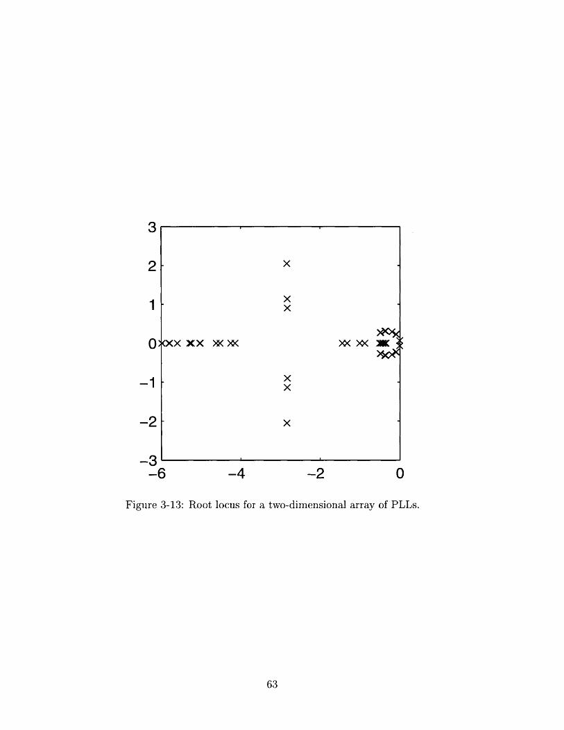
3
2 [
1
00xx xx
-1
-3'-6 -4 -2 0
Figure 3-13: Root locus for a two-dimensional array of PLLs.
63
x
xx
xx
X

1 2
4113
Clock Signal
Node 1
Node 2
Node 3
Node 4
Time
Figure 3-14: Mode-locking example
Fig. 3-5, and its associated matrices:
/ -1
1
1
0
0
0
-1
0
1
0
0
0
-1
0
1
0
0
0
-1
-1 /
A 2 = A =
Because phase is periodic with period 27r, the p
tors A0 = A 1# mod 27r. For small 0, (A1 # mod
irrelevant. However, consider #,, = [0, 7r/2, -7/2,
-1 1 1 0 0
o -1 0 1 0(3.11)
0 0 -1 0 1
o 0 0 -1 -1
hase measured at the phase detec-
2 -) = A10, so the nonlinearity is
7r]T. Because of the nonlinearity,
A 2 (A1 # mod 27r) = A 2 [0, -r/2, r/2, -7/2, 7r/2]T = 0 (3.12)
so 0_, is a stationary point. This is intuitively easy to see, in reference to Fig. 3-14:
each oscillator leads one neighbor, and lags behind another neighbor by exactly the
same amount. The net phase error is zero, so clearly there is no restoring force to drive
the oscillators into phaselock. Furthermore, this equilibrium point is stable, because
the nonlinearity does not change for small deviations from 02 so dynamics about 0-
are the same as those about 0. The locking of a distributed oscillator to non-zero
relative phases has been called mode-locking [40]. At startup, each oscillator in a
64

distributed PLL starts at a random phase, so there is a nonzero chance of converging
to a mode-locked state. Simulations show that for a network like the one shown here,
the system ends modelocked from ~ 1/3 of random initial states. The probability
goes up rapidly with the the size of the system; a 4 x 4 array ends up modelocked
well over 99% of the time.
Pratt and Nguyen proved several useful properties about systems in mode-lock.
The lemmas and theorem are repeated here with outlines of proofs, generalized to
include arbitrary (rather than Cartesian) networks.
Consider a system of oscillators to be a circuit, with oscillators at the nodes,
and connections between oscillators to be branches. (This is the same model as was
presented in Section 3.3.1). The phase counterpart to Kirchhoff's Voltage Law is:
Lemma 1 The sum of branch phase differences must be a multiple of 27r.
The sum is a multiple of 27r rather than 0 because phase differences here are defined
over a range [-7r, 7r), so at any branch 27r might be added or subtracted to bring the
result into the right range. For example, a phase detector will measure the difference
between 57r/6 - (-57/6) =wr/3, not 57r/3. This is true independent of mode-lock.
The second lemma derives from conditions for mode-lock: that is, the nodes are
in static equilibrium although the phases are not identical.
Lemma 2 If a set of oscillators is mode-locked, there must be at least one loop in
the network for which the sum of phase differences is a nonzero multiple of 27r.
The proof is as follows: in mode-lock, by definition, the nodes are not all at the
same phase. Therefore, there must be at least one node which connects to a branch
with nonzero phase error. Call that Node 1. Because Node 1 is in equilibrium by
definition of mode-lock it must connect to at least one branch with a positive phase
error. That branch connects to some Node 2, and appears as a negative phase error
there. Since Node 2 is also in equilibrium, it must have some other branch with an
offsetting positive phase error. Because there is a finite number of nodes, the loop
will eventually close back on Node 1. By Lemma 1, the sum must be a multiple of
65

27r. Because by construction, all the branches were positively-oriented, the sum must
be nonzero [40].
There are a number of ways to avoid mode-lock. The most obvious one is to simply
break the feedback: a consequence of Lemma 2 is that if there are no feedback loops,
there can be no modelock. This is not an attractive solution because, as shown in
the example with a one-dimensional array, full feedback helps average and attenuate
noise, so it would be best to avoid modelock without affecting the interconnection
of the system or the operation when correctly phase locked. One possible solution
would be to have a special startup state where there is no feedback between oscillators,
and then an operational state with full feedback. The system might be synchronized
during the startup, and then would remain phase-locked in the operational state. The
biggest drawback of this approach is that the the transition from the reset state to the
operational state jolts the system, and could push it into mode-lock. Thus, it would
be preferable to have a solution that does not require changing network topology even
temporarily. Fortunately, there is such a way.
If we define a minimal loop as a loop in the graph that cannot be decomposed
into other loops, we can combine the results succinctly into:
Theorem 1 For a system in mode-lock, there must be a phase difference 0 between
two oscillators such that 0 ;> 2/n where n is the number of nodes in the largest
minimal loop in the network.
By Lemma 2, there must be at least one loop (L) with a phase difference sum of at
least 27. If it has more than n nodes, it cannot be a minimal loop. Decompose L into
L1 and L 2. By Lemma 1, the loop sum around both L1 and L 2 must be an integral
multiple of 27, so at least one of them must have a loop sum of at least 27r; iterate
if necessary to get a loop of n or fewer nodes. Since the sum of the branch phase
differences must be 27r, at least one of the branches must have a phase difference of
at least 27r/n.
Theorem 1 suggests a way to distinguish between mode-locked states and the
desired 0-phase state: in mode-lock, there must be at least some large phase errors
66

across individual branches. If the gain of the phase detector is designed to be negative
for a phase difference larger than 0, then all mode-locked states are made unstable
without affecting the in-phase equilibrium. Pratt and Nguyen suggest that an XOR
phase detectors precludes modelock in a rectangular network of oscillators because the
response decreases for phase errors larger than 7r/2,[40]. This result follows directly
from Theorem 1: in a rectangular array, the largest minimal loop has 4 nodes, so
0 = 27/4 = 7r/2. Two other phase detectors are described in the next chapter, both
with 0 < 7r/2, which would be useful in non-rectangular networks, and where more
gain near 0 phase is desirable.
67

68

Chapter 4
Implementation and Testing
Distributed Clocks
Two test chips were made to explore implementation issues: how much power do the
oscillators require? How much area is needed for the compensation filters? Can a
real loop, with the buffer and wire delays be stabilized? The first was a 4-oscillator
chip in a 0.6pm double-poly CMOS process with a clock speed up to 350 MHz, and
the second was a 16-oscillator chip in a 0.35pam single-poly CMOS at clock speeds of
1.2-1.4 GHz. The two chips are described in turn below.
4.1 4 Oscillator Chip
The 4 oscillator chip was done as a proof of concept to show correct phase locking in
the simplest system that could possibly be vulnerable to modelock; a plot is shown
in Fig. 4-1 It consists of four nodes (each with an oscillator and loop filter) and
five phase detectors (one between each pair of neighbors, and one connected to an
external input). High-speed probes contact chip pads at the edges of the chip. One
probe drives the input, and the other three are connected to outputs of the oscillators.
(The probes are too large to connect more than one probe on a single chip side, so
all four oscillators could not be measured at the same time.)
69

Figure 4-1: Micrograph of the 4 oscillator, 350 MHz chip
70

4.1.1 Oscillator
The primary metric in the design of oscillators for clock generation is jitter, and
the majority of that is due to power supply noise [64, 65]. Integrated LC oscillators
often have a lower noise floor than other on-chip oscillators, but substrate and supply
noise are dominant on a large digital chip. Ring-type or relaxation oscillators are
usually preferred for on-chip clocks because large chips are usually sorted into different
categories based on measured achievable clock speed, and LC oscillators are more
difficult to tune. For this chip, a differential relaxation oscillator was chosen because
Hspice simulations showed that this relaxation oscillator had better power-supply
rejection than did ring oscillators. The relaxation current-controlled oscillator, or
"CCO," is shown in Fig. 4-2. Transistors M 3 , M 4 , M 5 , and M6 , along with capacitor
C make up a conventional source-coupled multivibrator, with M7 and M8 as active
loads and nbias controlling oscillation frequency through Id3,4. The drawback is that
that circuit has a feedthrough of -6dB to nodes V+ and V- from VDD, and almost
OdB to the capacitor from ground via Cbs of M 3,4 , so supply noise rejection is poor.
In the proposed oscillator, M1 and M2 provide shunt-shunt feedback around M 3 and
M4 respectively, lowering the output impedance at V+ and V- to 1/gm. D1 and D2
limit the amplitude of oscillation to avoid saturation of M 3 and M4 . Frequency can
be adjusted by adding common-mode current into nodes V+ and V-.
Oscillator layout is shown in Fig. 4-3. Layout for both halves of the oscillator
is identical, and the halves are immediately adjacent. Good matching between the
halves corresponds to a 50% duty cycle. Furthermore, all source/drain regions were
shared to minimize layout area and parasitic capacitance.
4.1.2 Phase Detector
As discussed previously, modelock can be avoided in regular arrays by using nonlinear
phase detectors whose response decreases monotonically beyond a phase difference of
7r/2 [40]. The phase detector Pratt and Nguyen suggest (a flip-flop delay and an XOR
gate) is not well-suited for integrated PLLs, however. First, it has relatively low gain,
71

Figure 4-3: Relaxation oscillator layout
72
... ......... ...... ......... ...... ......... ...... ............ ......... ...... ............ ......... ...... ......... ...... ......... ...... ......... ...... ......... ...... ......... ...... ......... ...... ......... ...... ......... ...... ......... .... ... ......... ......... .. .................. ......... ......... .. ......... ............ ......... ......... .. ......... ............ ....
...........................................
....................
.................................

so mismatch can lead to large input-referred phase offsets. Second, it generates full-
swing digital signals at half the clock frequency; this digital noise must be attenuated
in the loop filter.
The phase detector proposed here,
A rshown in Fig. 4-4, has the right nonlin-
pbias M7 M8 earity, higher gain at small A0q and has
much less high-frequency content than
D2 an XOR. The noise that is generated is
V+ V- at the clock frequency, and is attenuated
an extra 6dB given the same first-order
M3 M4 loop filter. (Only half of the circuit is
drawn. The other half is the symmetri-
M1 M2 cal counterpart, with clocki and clock2
switched.) M1 , M 2, and M3 comprise
an arbiter. The voltage at node A is
C buffered, sampled, and converted to a
current, so that multiple inputs can beM5 M6
nbias summed at each oscillator node. Syn-
chronous sampling of the arbiter output
by M 6 and M 7 demodulates it, removing
Figure 4-2: Relaxation oscillator schematic high frequency content. Timing wave-
forms are shown in Fig. 4-5. The phase of the sampling instant affects the transfer
function, shown in Fig. 4-6. Node A is the output of the arbiter. When clocki and
clock2 are nearly in phase, as is the case at sample periods 1 and 2, A is sampled while
its value is still valid, so the output Y goes from 0 to 1 over the width of the arbitration
window. Hence, the phase detector has a high gain near 0 phase difference. As the
phase difference increases, sampling instance timing becomes relevant. A is sampled
at a fixed delay from the rising edge of clocki. If clock2 falls before A is sampled, the
output Y will also fall, as shown for periods 3 and 4. Therefore, 0c, the phase angle
at which the output transfer function starts to fall, depends on the relative timing
73

U
Ml
A M5
Tick M6
M2
M7 "
I2 M34
13 T ___M4
I4I5 I6
N1
I7 I8 I9
M8
M9
M1 M12
M10
Figure 4-4: Phase detector schematic
of the falling edge of clock2 and the sample delay. If 0, is the phase of the sampling
instant and Of the phase of the falling edge, Oc = O - O, so the characteristic angle
could be adjusted easily simply by setting the delay through I ... 19. With 0, ~ 7r/2
and a 50% duty cycle (i.e., Of = ir) 0c would be ir/2, which is the constraint to avoid
modelock. Were smaller 0, needed to accommodate a different network structure, the
same circuit could be used with a different 0,. Adding the output from the unshown
half of the circuit gives the other half of the phase response, shown in Fig. 4-7. The
full circuit fits in 80pm x 40pam.
4.1.3 Loop Filter
One loop filter is associated with each CCO. Conventional loop filters use a charge
pump with an RC pole-zero pair, and often put the large capacitor and resistor off
74

Clockl
Clock2
A
Sample
Y
1 2 3 4 5
Figure 4-5: Phase detector timing waveforms
Iout
-7t 1 293 4C Phase
Figure 4-6: Sampled phase detector half-circuit transfer function
chip. To avoid inconveniently large resistor and capacitors, a feed-forward compensa-
tion method was used. The loop filter of Fig. 4-8 consists of two differential amplifiers.
(Note that because the frequency control to the oscillator consists of two currents,
both amplifiers have twin outputs.) M 3 , M 4 , M 5 , and M6 make up amplifier A 1 ,
biased by M!, while M1 , M 2 , M 7 , M8, M 1 and M 12 make up A2 , biased by M10 .
The differential output currents from the phase comparators at the edges of each tile
are summed at nodes I,-+ and fln- and drive both amplifiers. A1 is a single stage
differential pair, so it has relatively low gain but a bandwidth limited by gm3,4/Cs3,4,
since nodes Ioutl and Iout2 drive a low impedance. A2 has two stages, much like a
prototypical op-amp. The first is biased at very low current to give high gain at DC
and allow the use of a relatively small compensation capacitor, and the second pro-
vides the needed gain and isolates the high impedance pole from the output. In this
75

Iout.
-IL -o T Phase
Figure 4-7: Sampled phase detector full transfer function
amplifier, the DC gain was simulated at 31dB with a 16kHz pole, a compensating zero
at 7.6MHz, and a high frequency pole well above the PLL target frequency. The use
of feed-forward compensation allowed the use of very small capacitors; the loop filter,
including the poly-poly capacitor, and the CCO with its output buffers together take
up 88pim x 8 8pm.
M7 M8
M11 M12
I1Io2
M3 M4 M5 M6
PT1 I M1 M2I in- I1 I 2 I in+
M9 M10Vb2 Vb1
Figure 4-8: Loop filter schematic
76
4.2 16 Oscillator Chip
The 16 oscillator chip was a second generation chip with a number of improvements
over the 4 oscillator first generation. First, a larger network provides a more thorough
test of modelock-resistance, because modelock is more likely from initial startup than
in smaller networks. Second, a newer and faster fabrication process, 0.35pm, was used,
to test the ideas at clock speeds more appropriate for modern microprocessors. Third,
key circuits were redesigned: the oscillator is a ring oscillator instead of a relaxation
oscillator, and no longer requires two levels of polysilicon; the phase detector now
uses a much simpler arbiter-based design that gives phase and frequency feedback as
appropriate.
4.2.1 Oscillator
The second chip used an NMOS-loaded differential ring oscillator as a voltage con-
trolled oscillator (VCO) (Fig. 4-10) primarily because only one layer of polysilicon
was used, and diodes were disallowed in an effort to make the circuits more amenable
to implementation in standard microprocessor. Transistors M 4 - M8 comprise the
differential inverter. The differential pair is M5 ,8 , the tail current is driven by M6 ,
and M 4,7 act as the NMOS load. The NMOS loads allow fast oscillation and shield
the output signal from VDD noise. Vbias is a low-pass version Of VDD generated by
subthreshold leakage through PFET M1 ; supply noise coupling in through Cgd of M4 ,7
is bypassed by M2 . The oscillation frequency is only dependent on the supply voltage
through capacitor nonlinearity and the output conductance of M 4 ,7, and feedback of
the PLL compensates drift of VDD and Vbias.
4.2.2 Phase Detector
Just like the phase detector for the 4-oscillator chip, the second generation phase
detector, shown in Fig. 4-11, has a sufficient nonlinearity, higher gain at small in-
put phase difference and less high-frequency content than an XOR phase detector.
Compared to Fig. 4-4, however, it is somewhat simpler in implementation, and has
77

Figure 4-9: Micrograph of the 16 oscillator, 1.3 GHz chip
78

M1M4 M7Vbias
M2 Vout
VoutM5 M8
Vctrl
M3
M6
Figure 4-10: Ring oscillator schematic
a smaller transistor count. It also has less delay from the clock inputs to the phase
detector outputs, which is important because the phase detector time constant helps
set the PLL feedback poles.
The core (M 1 - M6 ) is an NMOS-loaded arbiter which acts as a nonlinear phase
detector. For no input phase difference, the output is balanced. As the phase differ-
ence increases from zero, one output will be asserted for the full duration of an input
pulse, while the other output will be asserted for only the remainder of the input pulse
duration after the first input pulse ends, which is equal to the input phase difference.
Thus the detector has very high gain near zero phase error that drops off to zero as
the input phase difference approaches the input pulse width (Fig. 4-12).
The pulse generators P and P 2 enable this arbiter to give frequency error feedback.
If one input is at a higher frequency than the other, its output will be asserted for
more input pulses than the other. Because the width of the pulses is independent
of input frequency, the average output voltage corresponds to frequency. Unlike a
typical phase-frequency detector, however, the strength of the error signal falls to
zero as frequency difference goes to 0, so there can be no modelock problems, yet
large signal frequency- (and hence, phase-) locking is enhanced. Fig. 4-13 shows
the large signal correction and small signal behavior of the entire array of PLLs as
79

M1M
Y1
I8M2 M5
............. MM
P1
M4
Y2
Ii
P2
Figure 4-11: Phase detector
the already internally-locked array approaches and locks to the reference clock. The
detector fits in 3Opum x 30pm.
4.2.3 Loop Filter
This loop filter, Fig. 4-14, is conceptually identical to the previous loop filter, Fig. 4-
8, though for biasing reasons, the wide bandwidth amplifier now has p-inputs and a
current mirror, and the high gain amplifier loads are cascoded.
M, - M5 make up amplifier A1 , while M9 - M17 make up A2 . The differential
output currents from the phase detectors at the edges of each tile are summed at
nodes In+ and In-, and drive both amplifiers. A1 is a single stage differential pair
so it has relatively low gain but a bandwidth limited by gm/Cgs. A2 has a high gain
cascoded stage driving a common source PFET M17. M1 6 is a large gate capacitor
which serves to set the dominant pole of M2 such that the PLL network is stable. M15
is biased at very low current to boost gain and enable a low time constant (as low
80

-. . - -.. ...... ..... ..
-. -.. ....... .... ........ ...
-. ........- ...- ... -. ... -. ....- ...
....... -.. ..... -.. ....-. .
-. ...-. ..-. .- ...- ..- ... -. . -. . -.. . -
OU
40
30CL
20(a0~3 10
0
U -10
-200
-30
-40
-50-0.
06
55
Small Signal Regime
05-
LargeSignal
4 Regime
04
35 - Referenceclock
0. 1 1 2 2
Figur
0.5 1 1.5 2 2.5 3 3.5Simulation time (microseconds)
e 4-13: Locking behavior of the PLL array
81
2 -0.1 0 0.1Time difference (nanoseconds)
Figure 4-12: Simulated phase transfer curve
1.
1.0
8 1.4)(A0
S.o00
0E5)
1.0
1.
0.2

M1 pbias M6
M2 M3
M7
In-
In+
M9 M10
M16M1l M12
AM10
M13 M14 M17
ML2
6 Out
M4 M5 M8 nbias M15
Figure 4-14: Loop filter schematic
as 12kHz) with a 15pm x 15pam gate capacitor. The simple design and feed-forward
compensation allow the loop filter to fit in only 15pm x 45pum. Each clock node,
consisting of an oscillator and a loop filter, takes just 45pum x 45pum.
82

Chapter 5
On-Chip Measurement of Clock
Performance
While increasing resources are devoted to implementing low skew and low jitter clocks
in modern microprocessors, there are few ways to measure jitter. Skew can be mea-
sured by such off-chip methods as e-beam [66] and photonic emission [67, 68], but
because both average thousands of edges, neither method is suitable for resolving
cycle-by-cycle clock jitter. A method to measure clock jitter was developed in this
thesis. A proof-of-concept test chip showed that excellent measurement performance
is possible, and this chapter describes the theory and results from that chip.
5.1 Introduction and Motivation
On-chip measurement necessarily
requires tricks. Acceptable clockAID
skew is generally around 10% of a 2
clock cycle and a microprocessor
clock period is typically 8-12 gate Figure 5-1: Time to voltage converter operationdelays. Hence, the measurement
necessarily requires timing resolution smaller than a single gate delay. Time-to-voltage
converters work by integrating a current onto a capacitor, as in Fig. 5-1 [69, 70, 71].
83

Delay Tune
CLK IDLL
E PD
Phase Interpolator
I
SiglnR[iJ Out [i]
Figure 5-2: Phase vernier
The capacitor starts with 0 voltage; at the beginning of the interval to be measured,
switch S1 closes, and the capacitor charges for the duration of the interval. Then S,
opens, the voltage is amplified, converted to a digital value and output, and then S2
closes to reset the capacitor. Such converters may have high dynamic range but do
not have enough resolution for clock jitter measurement, essentially because the time
of interest is comparable to the time it takes to open and close switch S 1.
Another approach is to sample the signal of interest into registers which are clocked
by closely-spaced sampling phases, as shown in Fig. 5-2. The interpolator takes in
several uniformly-placed phases and generates a larger number of phases with closer
spacing. The newly generated phases are used to clock a string of registers, marked
R[i] in the figure. The timing of a transition on SigIn can be deduced to within
the spacing of the sampling phases. Effectively, the registers compare the transition
instant of the input signal Sigln to a set of fixed times, just as a flash analog-to-digital
converter (ADC) compares an input voltage to a set of voltage thresholds. Because
of the similarity, it is useful to think of this architecture as a flash time-to-digital
84
I I
I I I I I I

converter, or TDC. Because the comparison thresholds are clock phases, this will be
called a sampling phase time-to-digital converter, or SPTDC. Either a delay-locked
loop with phase interpolation (as shown) or an array oscillator can be used to generate
sampling phases with time differences smaller than a single gate delay [72, 73, 74, 75].
However, mismatches between the oscillators in the array or delays in a DLL can be
significant, giving as much as a gate delay offset before calibration [72].
The approach presented here is also a flash TDC, but rather than creating the
time vernier by generating closely-spaced clocks, the vernier arises from input-referred
offset on the samplers. Hence, the proposed converter will be called a sampling offset
time-to-digital converter, or SOTDC. The advantage is that instead of needing to
generate precise clocks, it is necessary only to create some sampling elements and
measure their relative positions. As will be demonstrated, measurement can be much
more precise than any calibration is likely to be. The SOTDC was developed to
measure jitter between clock domains, but it works to measure the timing of any
signal relative to a reference.
5.2 Time-to-Digital Converter Fundamentals
Calibration and operation of the SOTDC depends critically on the operation of the
sampling elements. (In Fig. 5-2, the sampling elements were registers, but they were
acting as arbiters.) An arbiter is a circuit that determines which of two inputs arrived
first. Because only the time difference between rising edges of the two inputs affects
the output, it is conventional to think of the arbiter as having a single input, where
that input is a time interval t between two incoming edges, as shown in Fig. 5-3(a).
Given enough time, the output of an arbiter settles to either a logic '1' or '0', indicating
whether the first or second input arrived first. Unfortunately, device mismatch gives
arbiters an effective time offset, t,,. Also, because of thermal noise, the output, y,
is not deterministic. y(t) = 1 if and only if t > t0, + t,, where t, is white noise with
standard deviation - [76, 77]. Therefore, the probability that the output y is a '1' is
85

1
0.8
21 y
Xt
0
time
(a) Arbiter input defini-tion
- 0.6
a'0.4
0.2 F
O'-2 -1 0 tos
t/O-1 2
(b) Probability that arbiter output is a 1
Figure 5-3: Arbiter definitions
) In2
Inl0 D D
tos tos
A A
tos
thermometer decode logic
Figure 5-4: TDC structure. "D" marks delay elements, and "A" the arbiters.
given by the Gaussian cumulative density function
P(y= 1) = 1+ erf ( -tos (5.1)
which is plotted in Fig. 5-3(b). The strong sensitivity of y to t near t = t0 s makes the
arbiter useful for precise time measurement.
Fig. 5-4 shows the simplified theory of operation of a flash TDC (cf. a flash ADC).
In any flash converter, the input is compared to a set of thresholds; call the thresholds
x. In a TDC, x is the set of offset times to which the input time t is compared. In
86
............. ..............

a SPTDC, each threshold xi is composed of a vernier delay D and an arbiter offset
t0,. Variation of t, is significant- the standard deviation of t0 s, at, is about 18ps in
0.35pm CMOS. Fig. 5-5(a) shows a plot of ideal x for an 8-level converter; Fig. 5-5(b)
shows the actual positions of the x with normally distributed t,,. Because the a-t
is large, errors in the x are significant. However, the random spread of t,, suggests
another approach to generating the x: eliminate the vernier delay entirely, and let
xi = t,2 . Fig. 5-5(c) shows typical x for such a converter,
5.3 SOTDC Yield
The random placement of xi in an SOTDC means that measurement precision varies
from chip to chip. Finding a formula for the expected yield given a desired precision
over a fixed range is surprisingly difficult. The problem is quite amenable to Monte
Carlo simulation, however. A simulated plot of expected yield vs. precision is shown
in Fig. 5-6.
5.4 Calibration of a SOTDC
Of course, a vernier-less, or sampling offset TDC is useless if it cannot be calibrated:
the outputs of the arbiters give information about the input signal in terms of the xi;
if the xi are unknown, the arbiter outputs are useless. Fortunately, it is possible to
find x empirically.
A TDC could be calibrated directly by connecting two signals with precisely-
known t and measuring resulting outputs for t over the range of interest. Fitting the
probabilities of an output '1' vs. t for each arbiter via Eq. 5.1 gives the effective x.
Unfortunately, input jitter adds linearly to the apparent measurement noise in this
case. In cases where it is impossible or inconvenient to input known signals, it is also
possible to calibrate a flash TDC indirectly with uncorrelated signals.
For uniformly distributed t, the probability that t is measured between two sam-
pling thresholds, P(xi+tn > t > xj+ts) A Pij(01), is proportional to xi-xj Aij for
87

U')7C3
0
00.a
x
0D
60-
40-
20-
0
-20
-40-
-602 4 6 8
(a) Ideal, xi oc i
0 2 4 6 8
(b) xi oc i + t,,, 18ps std. dev.
2 4 6 8
(c) xi = t,, 18ps std. dev.
Figure 5-5: x(i) vs. i
88
40
20
0
(i2
00-(D~U,0
x
-a-20
-4C 7
40-
30-
20-
10
0
c0
0.
a,
-10C

3 4precision (ps)
Figure 5-6: Expected yield of anstandard deviation.
SOTDC, for a fixed precision over a range of one
a single event, as long as the difference is much larger than sampling noise, Aj > t,.
For example, if the two input signals are constant-frequency square waves, measure-
ments with bit i low and bit j high will occur with a frequency of Aijfif 2 where fi
and f2 are the frequencies of the two input signals. While x can be fully deduced
from such measurements, the resolution is poor for Aj e t,,.
A second indirect calibration method resolves small Aij in terms of o-. When Aij
is comparable to t, there will sometimes be a "bubble" in the output codeword;
that is, it will appear that xj + t, > t > xi + t, even though xi > x3 . The ratio
r = Pi(10)/Pij(01) should depend only on 6 = Ai\j/-, and in fact, it does.
Consider two arbiters with ti = x, + ti and t2 = X2 + tn2.
instantaneous switching thresholds of the arbiters, so
P(y1 = 1) = P(t > ti)
P(y2 = 0) = P(t < t2 )
P(y1 = 1 ,y2 = 0) A P12 (10) = P(ti < t < t2)
P12 (10) = P(ti < t2) - P(ti < t < t2 I t1 < t2)
t1 and t2 are the
(5.2)
(5.3)
(5.4)
(5.5)
89
1
0.8
0.6V
0.4
0.2
-2 5 6'

Let x =t2- t1 . Then x is Gaussian with mean x 2 - x 1 = At and standard deviation
2u. For uniformly distributed t, P(ti < t < t 2 ti < t 2 ) Oc t 2 - t1 . Substituting into
Eq. 5.5,
P12 (10) Oc x - P(X > 0) (5.6)
Oc x e 4a 2 dx (5.7)
Oc je (4a2)+ At1 + erf (5.8)VIT2 ( 2or
By symmetry, P12(01)1 ,t= P 12 (10)1,,-,. Defining 6 = and erfcx(x) = ex 2 2 f: et 2 dt
gives
) P 12 (10) 1+ VF -erfcx(-6)r (6) = =_ (5.9)P 12 (01) 1 - F6 -erfcx(6)
In this way an array of arbiters can be calibrated to much higher precision than their
manufacturing tolerances without the use of precise input clocks.
Thus, by measuring r and inverting Eq. 5.9, one can find relative spacings of x
in terms of a. Combined with either of the previous two methods calibrations, this
measurement thus gives a and precise measurements of x. Note that both indirect
methods are completely insensitive to input jitter.
5.5 Circuit and Results
The SOTDC circuit consists of a set of nominally identical arbiters and output cir-
cuitry to transfer the bits off-chip. The implemented symmetric CMOS arbiter is
shown in Fig. 5-7. The outputs are precharged when Inl and In2 are low (for clock
systems where jitter is meaningful, there will be substantial overlap between the low
phases of the inputs). The first edge that arrives pulls down the corresponding out-
put, and the positive feedback guarantees that eventually a valid logic value can be
latched from the output. For the test chip, 64 such arbiters were connected in parallel
90

M1 M4
Y1 Y2
M2 M5
Inl MM6 In2
Figure 5-7: Symmetric CMOS arbiter
to two test inputs, and their outputs individually recorded.
Fig. 5-8 shows x for one test chip measured directly. As expected, process vari-
ations distribute the x over a range of approximately 50 picoseconds. A plot of x
calculated by numerically inverting Eq. 5.9 for measured data vs. x measured directly
is shown in Fig. 5-9. The fit is perfect to within the tolerances of the measurement
equipment; clearly, calibration by random signals is viable. Best fit - is 0.35 picosec-
onds, which corresponds to an arbiter aperture of ~ lps, consistent with a previously
reported simulated value of 10ps in a 3pm CMOS process. Nonuniform spacing of the
arbiter thresholds limits resolution of this TDC to 2ps over the range [-15ps,15ps].
The goal of this part of the thesis was to measure jitter in the 16 oscillator chip
described in Chapter 4. A set of arbiters was connected between the clocks of neigh-
boring tiles, and a 128-word DRAM recorded arbiter results. Unfortunately, the
DRAM timing was marginal on that test chip, so direct measurements were unavail-
able.
91

70
60
50
40
30
20
101-
-40 -20 0 20threshold x(i), picoseconds
40
Figure 5-8: Measured xi, with expected curve for 18ps standard deviation of t,,.
20
o6
0
.3LU
C)
CO)
10 1
0
-10
-20'-40 -20
)
0 20 40directly-measured x(i)
Figure 5-9: Measured xi vs. xi derived via Eq. 5.9, for a- = 0.3 5ps
92
00
0
I
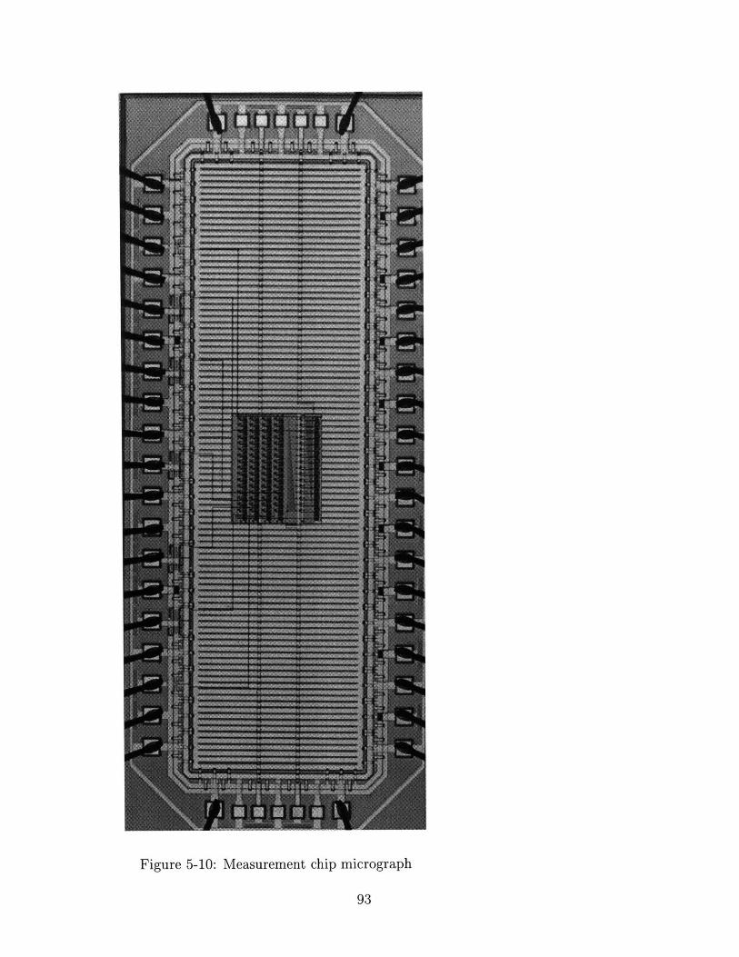
Figure 5-10: Measurement chip micrograph
93

94
Chapter 6
Conclusions
6.1 Summary and Contributions
A great deal of work has been done previously on clocks in integrated circuits. As the
ratio of clock period to wire-delay across a chip decreases, more and more attention
is being devoted to clocking. An attempt was made in this thesis to look forward, to
predict the clocks necessary in the near future to continue the trend of faster devices
and faster clocks.
One contribution of this thesis has been the analysis of clock networks in terms
of performance given parameter variations and noise. Although much of the focus
has been on the contrast between different clock networks, the conclusion is that
the different architectures do not replace but rather complement each other. Over
a single tile where signal propagation delay is small compared to the clock period
and all points must be synchronized, tree distribution is effective. For relatively long
distances on a chip, clock regeneration becomes useful to filter out high frequency
noise on the distribution wire. A multiple-oscillator peer network also avoids the
problem of having different paths to nearest neighbors that plagues trees. Gridded
distribution, or more generally shorting together spatially separated buffers greatly
reduces skew and jitter between tiles as long as the initial offsets are small.
Another contribution is the analysis and implementation of a clock network that
uses distributed generation. Theory about mode-locking was extended to account for
95

non-orthogonal networks. Inter-oscillator coupling was treated in the context of a
single multivariable system which exposes all possible interactions. The phase detec-
tor and oscillator were modified from standard versions to satisfy the requirements
needed for a distributed clock. Although the details will likely be changed (short-
ing together the tiles and finding another way to measure phase differences between
clocks is an obvious improvement) the main strength of this architecture is that the
clock traverses the same path, peer-to-peer, as does the data. Because the clock can
be measured and corrected over multiple cycles, however, it appears that clock skew
can always be corrected to a fraction of the uncertainty in data delay. In other words,
it should always be possible to distribute a clock using the same technology as is used
for long-distance interconnect.
Verification of clock design will likely become more important as a way to con-
firm predictions about clock performance. The proposed and tested sampling offset
time to digital converter appears to be well-suited to this task, with resolution of a
small fraction of a single gate delay. Because of its extreme hardware simplicity and
generality, the SOTDC may find its way onto many chips as a simple debugging tool.
6.2 Future Work
This thesis was dominated by analysis and implementation of the distributed clock
network, and of how that network compares with conventional clock networks. This
leaves a two-fold opening for future work: more accurate testing and comparison to
conventional clock networks, and the development clock architectures that are as yet
impractical.
6.2.1 Testing and measurement
The focus of the design and testing of the multiple-oscillator array was on initial
locking and stability. Testing received substantially less attention. Another version of
that chip with a more robust DRAM (so that precise timing data could be obtained),
and controllable, on-chip noise generators (i.e., large transistors between power and
96

ground) would help calibrate the noise models.
On a similar topic, distributed PLLs make low-speed functional testing difficult.
For distributed clock generation to move to production, stability of the network at
low-speeds should be addressed. It's trivial to add a controllable divider for each node
oscillator; however, the extra delay will certainly make the network unstable unless
other changes are made.
6.2.2 Unconventional Clocks
Grids and clock trees have found widespread use in industry already. A number of
other clocking strategies have been proposed that may either find use in niche appli-
cations, or perhaps someday take over as the dominant clock method if technology
evolves to makes them more attractive.
Salphasic
Salphasic clocking is conceptually related to equipotential clocking. If the wires are
lossless but the transmission line delay is causing clock skew, it is possible to set up
standing waves in the clock network. Because these standing waves are perfectly syn-
chronous with the signal at the driver, a clock can be distributed over long distances
with no skew. Of course, this depends on having lossless transmission lines for clock
distribution; this constraint can be approximated closely in systems on the scale of
several meters with clocks in the tens of megahertz [36]. On chip, however, resistance
in the wires has made salphasic clocking untenable.
Resonant Clocks
Resonant clocking is a similar approach, intended for a different purpose. A standing
wave is set up in a transmission line with a period equal to the desired period of a
clock. With care, a transmission line can be tuned to resonate a fundamental and
several odd harmonics in phase, despite the capacitive load and small resistive losses
in the wire so that a true square wave appears at the load [37]. A resonant clock in
97

a low-loss transmission line dissipates a fraction of the CV 2f power that traditional
clock networks do. The technique is relatively new, and has not been proven to be
practical at high speeds.
Optical Clocking
Because the propagation speed of optical signals is easily controlled, optical clocks
have been suggested as a way to equalize path delay and thus minimize clock skew [38,
39]. Optical signals, transmitted either in a tree, as in the first citation, or in free space
as in the second, also have the advantage that they do not interfere with each other,
and are immune to electrical or magnetic coupling. Unfortunately, the conversion
from optical signals to electrical is a significant stumbling block. Detectors for optical
signals are not silicon, and hence require a substantial fabrication process change.
Second, the conversion is often relatively slow and error prone because the detected
currents are small. No optical clock has been demonstrated for VLSI, although optical
clocks may become practical in the future.
98

Bibliography
[1] Neil H. E. Weste and Kamran Eshraghian. Principles of CMOS VLSI design.
Addison Wesley, 2 edition, 1990.
[2] Daniel W. Bailey and Bradley J. Benschneider. Clocking design and analysis for
a 600 MHz Alpha microprocessor. Journal of Solid State Circuits, 33(11):1627-
1633, November 1998.
[3] Stephen H. Unger and Chung-Jen Tan. Clocking schemes for high-speed digital
systems. IEEE Transactions on Computers, C-35(10):880-895, October 1986.
[4] Arthur F. Champernowne et al. Latch-to-latch timing rules. IEEE Transactions
on Computers, 39(6):798-808, June 1990.
[5] E. G. Friedman. The applications of localized clock distribution design to im-
proving the performance of retimed sequential circuits. In Proceedings of the
IEEE Asia-Pacific Conference on Circuits and Systems, pages 12-17, December
1992.
[6] Karem A. Sakalh et al. Synchronization of pipelines. IEEE Transactions on
Computer-Aided Design, 12(8):1132-1146, August 1993.
[7] Jose Luis Neves and Eby G. Friedman. Topological design of clock distribution
networks based on non-zero clock skew specifications. In Proceedings of the 36th
Midwest Symposium on Circuits and Systems, pages 468-471, August 1993.
99

[8] Narendra V. Shenoy, Robert K. Brayton, and Alberto L. Sangiovanni-Vincentelli.
Resynthesis of multi-phase pipelines. In Proceedings of the ACM/IEEE Design
Automation Conference, pages 490-496, June 1993.
[9] C. Thomas Gray et al. Timing constraints for wave-pipelined systems. IEEE
Transactions on Computer-Aided Design, 13(8):987-1004, August 1994.
[10] Michel R. Dagenais and Nicholas C. Rumin. On the calculation of optimal
clocking parameters in synchronous circuits with level sensitive latches. IEEE
Transactions on Computer-Aided Design, 8(3):268-278, March 1989.
[11] Karem A. Sakallah, Trevor N. Mudge, and Oyekunle A. Olukotun. Analysis and
design of latch-controlled synchronous digital circuits. IEEE Transactions on
Computer-Aided Design, 11(3):322-333, March 1992.
[12] Tolga Soyata and Eby G. Friedman. Retiming with non-zero clock skew, vari-
able register, and interconnect delay. In Proceedings of the IEEE International
Conference on Computer-Aided Design, pages 234-241, November 1994.
[13] Francois Angeau. A synchronous approach for clocking VLSI systems. Journal
of Solid State Circuits, SC-17(1):51-56, February 1982.
[14] H. B. Bakoglu, J. T. Walker, and J. D. Meindl. A symmetric clock-distribution
tree and optimized high-speed interconnections for reduced clock skew in ULSI
and WSI circuits. In VLSI in Computers and Processors, pages 118-122, Rye
Brook, NY, October 1986. IEEE International Conference on Computer Design.
[15] Allan L. Fisher and H. T. Kung. Synchronizing large VLSI processor arrays.
IEEE Transactions on Computers, C-34(8):734-740, August 1985.
[16] Ahmed El-Amawy. Clocking arbitrarily large computing structures under con-
stant skew bound. IEEE Transactions on Parallel and Distributed Systems,
4(3):241-255, 1993.
100

[17] Daniel W. Dobberpuhl et al. A 200-MHz 64-b dual-issue CMOS microprocessor.
Journal of Solid State Circuits, 27(11):1555-1567, November 1992.
[18] Bradley J. Benschneider et al. A 300-MHz 64-b quad-issue CMOS RISC micro-
processor. Journal of Solid State Circuits, 30(11):1203-1214, November 1992.
[19] Paul E. Gronowski et al. A 433-MHz 64-b quad-issue RISC microprocessor.
Journal of Solid State Circuits, 31(11):1687-1696, November 1996.
[20] Donald F. Wann and Mark A. Franklin. Asynchronous and clocked control struc-
tures for VLSI based interconnection networks. IEEE Transactions on Comput-
ers, C-32(3):284-293, March 1983.
[21] S. Y. Kung and R. J. Gal-Ezer. Synchronous versus asynchronous computation
in very large scale integrated (VLSI) array processors. Proceedings of SPIE,
341:53-65, May 1982.
[22] Sanjay Dhar, Mark A. Franklin, and Donald F. Wann. Reduction of clock delays
in VLSI structures. In IEEE International Conference on Computer Design,
pages 778-783, October 1984.
[23] Mehdi Hatamian and Glenn L. Cash. Parallel bit-level pipelined VLSI designs for
high-speed signal processing. Proceedings of the IEEE, 75(9):1192-1202, Septem-
ber 1987.
[24] Eby G. Friedman and Scott Powell. Design and analysis of hierarchical clock
distribution system for synchronous standard cell/macrocell VLSI. Journal of
Solid State Circuits, SC-21(2):240-246, April 1986.
[25] Michael A. B. Jackson, Arvind Srinivasan, and E. S. Kuh. Clock routing for high-
performance ICs. In 27th Proceedings of the ACM/IEEE Design Automation
Conference, pages 573-579, June 1990.
[26] Fumihiro Minami and Midori Takano. Clock tree synthesis based on RC delay
balancing. In Proceedings of the IEEE Custom Integrated Circuits Conference,
pages 28.3.1-28.3.4, May 1992.
101

[27] Ting-Hai Chao, Yu-Chin Hsu, Jan-Ming Ho, Kenneth D. Boese, and Andrew B.
Kahng. Zero skew clock routing with minimum wirelength. IEEE Transactions
on Circuits and Systems-Il: Analog and Digital Signal Processing, 39(11):799-
814, November 1992.
[28] Jason Cong, Andrew B. Kahng, and Gabriel Robins. Matching-based methods for
high-performance clock routing. IEEE Transactions on Computer-Aided Design,
12(8):1157-1169, August 1993.
[29] Ren-Song Tsay. An exact zero-skew clock routing algorithm. IEEE Transactions
on Computer-Aided Design, 12(2):242-249, February 1993.
[30] Andrew B. Kahng and C.-W. Albert Tsao. Practical bounded-skew clock routing.
Journal of VLSI Signal Processing, 16(2/3):87-103, June/July 1997.
[31] Shantanu Ganguly, Daksh Lehther, and Satyamurthy Pullela. Clock distribu-
tion methodology for the PowerPC microprocessors. Journal of VLSI Signal
Processing, 16(2/3):181-189, June/July 1997.
[32] Earl T. Cohen et al. A 533MHz BiCMOS superscalar microprocessor. In ISSCC
Digest of Technical Papers, pages 164-165, February 1997.
[33] Charles F. Webb et al. A 400MHz S/390 microprocessor. In ISSCC Digest of
Technical Papers, pages 168-169, February 1997.
[34] Toyohiko Yoshida et al. A 2V 250MHz multimedia processor. In ISSCC Digest
of Technical Papers, pages 266-267, February 1997.
[35] G. Geannopoulos and X. Dai. An adaptive digital deskewing circuit for clock
distribution networks. In ISSCC Digest of Technical Papers, pages 400-401,
February 1998.
[36] Vernon L. Chi. Salphasic distribution of clock signals for synchronous systems.
IEEE Transactions on Computers, 43(5):597-602, May 1994.
102

[37] M. E. Becker and T. F. Knight, Jr. Transmission line clock driver. In IEEE
International Conference on Computer Design, pages 489-490, October 1999.
[38] C.-S. Li, F. Tong, K. Liu, and D. G. Messerschmitt. Fanout analysis of multi-
stage optical clock distribution using optical amplifiers. In Globecom, pages
434-438, 1991.
[39] Helmut Zarschizky, Christian Gerndt, Martin Honsberg, and Ekkehard Klement.
Optical clock distribution with a compact free space interconnect system. In
IEEE Lasers and Electro-Optics Society Annual Meeting, pages 590-591, 1992.
[40] Gill A. Pratt and John Nguyen. Distributed synchronous clocking. IEEE Trans-
actions on Parallel and Distributed Systems, February 1995.
[41] David G. Messerschmidt. Synchronization in digital system design. IEEE Journal
Selected Areas in Communications, 8(8):1404-1419, October 1990.
[42] Morteza Afghahi and Christer Svensson. Performance of synchronous and
asynchronous schemes for VLSI systems. IEEE Transactions on Computers,
41(7):858-872, July 1992.
[43] D. Boning and S. Nassif. Models of Process Variations in Device and Intercon-
nect, chapter 6. IEEE Press, 2000.
[44] Brian E. Stine et al. Simulating the impact of poly-CD wafer-level and die-level
variation on circuit performance. In Second International Workshop on Statistical
Metrology, June 1997.
[45] M. Eisele, J. Berthold, R. Thewes, E. Wohlrab, D. Schmitt-Landsiedel, and
W. Weber. Intra-die device parameter variations and their impact on digital
CMOS gates at low supply voltages. In Technical Digest of IEDM, pages 67-70,
1995.
[46] Duane S. Boning and James E. Chung. Statistical metrology - measurement
and modelling of variation for advanced process development and design rule
103
generation. In Proceedings of the International Conference on Characterization
and Metrology for ULSI Technology, March 1998.
[47] Tomohisa Mizuno, Jun-ichi Okamura, and Akira Toriumi. Experimental study
of threshold voltage fluctuation due to statistical variation of channel dopant
number in MOSFET's. IEEE Transactions on Electron Devices, 41(11):2216-
2221, November 1994.
[48] Martin Eisele, J6rg Berthold, Doris Schmitt-Landsiedel, and Reinhard
Mahnkopf. The impact of intra-dive device parameter variations on path delays
and on the design for yield of low voltage digital circuits. IEEE Transactions on
VLSI, 5(4):360-368, December 1997.
[49] Xinghai Tang, Vivek K. De, and James D. Meindl. Intrinsic MOSFET parameter
fluctuations due to random dopant placement. IEEE Transactions on VLSI,
5(4):369-376, December 1997.
[50 D. C. Keezer and V. K. Jain. Design and evaluation of wafer scale clock dis-
tribution. In Proceedings of the IEEE International Conference on Wafer Scale
Integration, pages 168-175, January 1992.
[51] Jos6 Luis Neves and Eby G. Friedman. Circuit synthesis of clock distribution
networks based on non-zero clock skew. In Proceedings of the IEEE International
Symposium on Circuits and Systems, pages 4.175-4.178, June 1994.
[52] Mohamed Nekili, Guy Bois, and Yvon Savaria. Pipelined H-trees for high-speed
clocking of large integrated systems in the presence of process variations. IEEE
Transactions on VLSI, 5(2):161-174, June 1997.
[53] Masakazu Shoji. Elimination of process-dependent clock skew in CMOS VLSI.
Journal of Solid State Circuits, SC-21(5):875-880, October 1986.
[54] Satyamurthy Pullela, Noel Menezes, and Lawrence T. Pillage. Reliable non-
zero skew clock trees using wire width optimization. In 30th Proceedings of the
ACM/IEEE Design Automation Conference, pages 165-170, June 1993.
104

[55] Masato Edahiro. Delay minimization for zero-skew routing. In Proceedings of
the IEEE International Conference on Computer-Aided Design, pages 563-566,
November 1993.
[56] Steven D. Kugelmass and Kennet Steiglitz. An upper bound of expected clock
skew in synchronous systems. IEEE Transactions on Computers, 39(12):1475-
1477, December 1990.
[57] Marios D. Dikaiakos and Kenneth Steiglitz. Comparison of tree and straight-
line clocking in long systolic arrays. Journal of VLSI Signal Processing, pages
1177-1180, 1991.
[58] Keith A. Bowman, Xinghai Tang, John C. Eble, and James D. Meindl. Imapact
of extrinsic and intrinsic parameter variations on CMOS system on a chip perfor-
mance. In Proceedings of the ASIC/SOC Conference, pages 267-271, September
1999.
[59] Marcel J. M. Pelgrom, AAD C. J. Duinmaijer, and Anton P. G. Welbers. Match-
ing properties of MOS transistors. Journal of Solid State Circuits, 24(5):1433-
1440, October 1989.
[60] Shy-Chyi Wong, Kuo-Hua Pan, Dye-Jyun Ma, M. S. Liang, and P. N. Tseng. On
matching properties and process factors for submicrometer CMOS. In Proceed-
ings of the 1996 IEEE International Conference on Microelectronic Test Struc-
tures, volume 9, pages 43-47, March 1996.
[61] Shih-Wei Sun and Paul G. Y. Tsui. Limitation of CMOS supply-voltage scal-
ing by MOSFET threshold-voltage variation. Journal of Solid State Circuits,
30(8):947-949, August 1995.
[62] M. Nekili, Y. Savaria, and G. Bois. Spatial characterization of process variations
via MOS transistor time constants in VLSI and WSI. Journal of Solid State
Circuits, 34(1):80-84, January 1999.
105
[63] Payman Zarkesh-Ha, Tony Mule, and James D. Meindl. Characterization and
modeling of clock skew with process variations. In Proceedings of the IEEE 1999
Custom Integrated Circuits Conference, pages 441-444, 1999.
[64] Ian A. Young, Monte F. Mar, and Bharat Bhushan. A 0.35pm CMOS 3-880MHz
PLL N/2 clock multiplier and distribution network with low jitter for micropro-
cessors. In ISSCC Digest of Technical Papers, pages 330-331, February 1997.
[65] Raghunand Bhagwan and Alan Rogers. A 1GHz dual-loop microprocessor PLL
with instant frequency shifting. In ISSCC Digest of Technical Papers, pages
336-337, February 1997.
[66] P. J. Restle, K. A. Jenkins, A. Deutsch, and P. W. Cook. Measurement and mod-
eling of on-chip transmission line effects in a 400 MHz microprocessor. Journal
of Solid State Circuits, 33(4):662-665, April 1998.
[67] Y. Uraoka, T. Maeda, I. Miyanaga, and K. Tsuji. New failure analysis technique
of ULSIs using photon emission method. In Proceedings of the International
Conference on Microelectronic Test Structures, volume 5, pages 100-105, March
1992.
[68] Yukiharu Uraoka, Isao, Miyanaga, Kazuhiko Tsuji, and Shigenobu Akiyama.
Failure analysis of ULSI circuits using photon emission. IEEE Transactions on
Semiconductor Manufacturing, 6(4):324-331, November 1993.
[69] Andrew E. Stevens, Richard P. Van Berg, Jan Van Der Spiegel, and Hugh H.
Williams. A time-to-voltage converter and analog memory for colliding beam
detectors. Journal of Solid State Circuits, 24(6):1748-1752, December 1989.
[70] C. Konstadakellis, S. Siskos, and Th. Laopoulos. A fast, versatile, CMOS time-
to-voltage converter. In Proceedings of the 6th Mediterranean Electrotechnical
Conference, pages 282-285, 1991.
[71] Elvi Rdissinen-Routsalainen, Timo Rahkonen, and Juha Kostamovaara. A time
digitizer with interpolation based on time-to-voltage conversion. In Proceedings
106

of the 40th Midwest Symposium on Circuits and Systems, pages 197-200, August
1997.
[72] Dan Weinlader, Ron Ho, Chih-Kong Ken Yang, and Mark Horowitz. An eight
channel 36Gsample/s CMOS timing analyzer. In ISSCC Digest of Technical
Papers, pages 170-171, 2000.
[73] Thomas A. Knotts, David Chu, and Jeremy Sommer. A 500MHz time digitizer
IC with 15.625ps resolution. In ISSCC Digest of Technical Papers, pages 58-59,
1994.
[74] Yasuo Arai and Masahiro Ikeno. A time digitizer CMOS gate-array with a 250 ps
time resolution. Journal of Solid State Circuits, 31(2):212-219, February 1996.
[75] J. G. Maneatis and M. A. Horowitz. Precise delay generation using coupled
oscillators. Journal of Solid State Circuits, 28(12):1273-1282, December 1993.
[76] Linsay Kleeman. The jitter model for metastability and its application to re-
dudnant synchronizers. IEEE Transactions on Computers, 39(7):930-942, July
1990.
[77] W. A. M. Van Noije, W. T. Liu, and S. J. Navarro, Jr. Precise final state
determination in mismatched CMOS latches. Journal of Solid State Circuits,
30(5):607-611, May 1995.
107

108

Appendix A
Full Schematics
A.1 4 oscillator chip
A.2 16 oscillator chip
109

A
VU-
p4hi1late phil philearly
Ef sam pled phase-com pphi2late phi2 phi2erly
I-I
m5
V
aCV
SiC0Si
SiAPhillate phil philearlyV sampled-phase-comp 141
Si L~j phi2late phi2 phi2early
AilAl 1
E o_0- 0
0
a- Q aC_
E0
o! a)
m im
03
9
phi<0>-U-.
~E0
L4
a_ 0 -
E0
a a0 WC(q
_E
U.
Em
IREF foster clock slowerskewfaster skewslower -
onode
1340
foster clock slower
v hillate phil philearlyL sopledphose-comp 144
ophi2te phi2 phi2eorlyAk--U
-U
(0
Figure A1.1: Top-level (chip core)
110
IREF foster clock slowerskewfaster skewslower
node
1470 0
faster clock slower
Ao
AV
A
W-
m_
I-
IREF foster clock slowerskewfaster skewslower
node
145 -
o 0
-0 -0
oe 0
foster clock slower
[REF foster clock slowerskewfaster skewslower
a rjnode
135 -0 0o 0
0 -0
V V)o 0
faster clock slower
-1 -

'"st. f.*lr locd1 b-,, , ~ 125 124-o.. -*'-p 4 'oad out __>c
slower nolood2 b' 3 Ifr
Figure A1.2: Node
T10/1.2 24/1 2 24/1.2
aa
12/0.6 12/0.6
24/0.6 24/0.6
gnd! gnd!
COpi cop2
nbias12/1.2
Figure A1.3: Relaxation oscillator
III
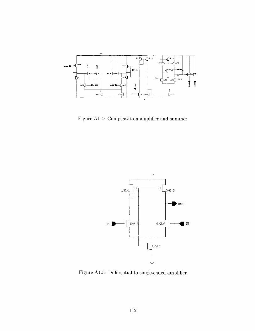
T
F/rA.4 meat. 1.- an m e
//1.8 6/1.8.
8/1.8 6~~~/1-8 .1. 18/. 1
15/1. 1512/ ./1.2
Figure A1.4: Compensation amplifier and summer
6/0.6 6/0.6
out
in 6/0.6 6/0.6 in
6/0.6
Figure A1.5: Differential to single-ended amplifier
112

1.2/3
2/.6 6phi2early
Outl Ophi lote
122/2
phil D phrl 1 all12
p~p~us-ephrlealy
Fiure A Sml paecmr
2/5 pp. /
ph 4 13
Fig11e A16Tapeehaecmaao
113

3/0.6 3/0.6
6/0,6 pi6/0.6
3/0 .6 3/0.6
gnd!
15phi2
116
Figure A1.7: Phase comparator core
114
phil -4 phi2
e

reirefcloc edrea% ,
dataswitv h
lut.ser~I< 12>UIotsoritt
:lockrefelc od-
datoswitc? t
-t.seil 13>srilotier Iq k
clock relrefelocV
reo I e
datoswit U-1136
C 0C c oC coc . .m rt ph 2 I 7 Ir ini 1121 phtI
slowom l phi,2lote lowerpher phaarly phi ear phillato slower phillate slowerfaster phillate faster pi2lt phile phileard
H ohl 1137 b0 0 1h2 rou c a a dr12 ma c
refelac r reteloc refefocZ rec* fca 11, reclo
Stch Ia wtch .5t data odatoswitch - datoswto * datoswltcb d-ta 5
S ut.seriol<21> "Ut.serfol<22> uk. erfol<2> luggerial424> 0out serial out.serial -- o tseria-l
R! CS 0 tla a a do i tdle kdck2oe
rout rI2UpthIl
slower poilar.y slower y Moto slower r phillate,ieryph Peah' ptieary
faster philiate phi2sar fster pilot foster ph' e p r
Shi31138 b 0d2 a i hi2 roua 0
re we r00 re -rarotore 0 .0 refoloc r
* ont r * cro wdat. a Ile tch 2 a - . data a QswItch a d Ed casWitch - a . r2 datoswitch -
eo uo at seril<F3l> * afserial432> ut~serol<33> £ aerfa 434>
ut -- eaa t.eria -- U .- a 1Uot.seralou o ut00 son a l
e h l c loe 0 clocktt Er a f tileaIlphlti~trout war ' 16 phi S w 119 phi l
slower phi2lote a: m a phillote slower pplear phillate
foster phillote phi2earl - a2lote phifear tster phIt2latehie I hi2 a r -a2 a
L4 re re
d 1
Iieil4> a10cl
MU C
data
ua erol 2>-111 'S T IhE0.
dot
uaFerio1443> aaE
0~a
0t ~
IF f ? rout phIi2 1- 1117 phi 1 1 1; '.lp*pl .try phi2 lte a 0 9 l pphil 2orL S h tlr phillate
. 11i p late phi2e . E - phi 2 at. philear - pki2eaty philearl - KphTi 014 t 00 k phl2lot k
f li 1t 14 phFS2 grou_ oropi ro c o
rTi
erial-44>- Z
L-i
lock
in.reok in.refelock
in.oTetI in ~dawF
in~dallosilitch in.dUoa-sw.TchR
I orwaOrdbackword
out.serial<11:13,212431:34.41:44>
p22late 116-y current-in n n
p p
Figure A2.1: Top-level (chip core)
115
rerefeloc 1111rea-
datow t
ut.se 1 1ucl ri
-Mot.i olI
clock
Wo
clock
clock

faster - faster
slower 0 -jslower
clock2refclock
readwrite
slower clock faster
clock -U--D clock
faster clock slower
1120|inclock- outclock
clock1114 1123
E-clock1 jmeasure At mux 1126 1127 128clock2 jAO Y out.serialrefclock Vn inv3x inv9xread out.somples --Iwrite
Figure A2.2: Individual tile
faster
comp amp- acobias -eE-iref phi ---- clockslowerringosc-2slower soe
Figure A2.3: Node
116
slower "
1129
clock
node-afaster "
a-

A./.3 / 0.7/0.35 0,7/0,35 4e- 13
0.7/0.35 0.7/0.35
slower 2.3/0.35 2.3/0.3 f stA vx1/1 8.4/0.35
A
8.4/0.35
slower
4203 1.8/0.6 1.0/0.6 faster4.2/0.35
4.2/0.35
1.5/0.35 1.5/0.35 .5'1.2 1.4/2.1
Figure A2.4: Compensation amplifier
Figure A2.5: Ring oscillator
117

VTloodbias W
out-
in+ 3.5/0.35
0.7/0.7
out+
3.5/0.35 in-
ibios 1/0.35
Figure A2.6: Differential inverter for the ring oscillator
17 115 n2d q - d q 117 nx119 118 n2inclodkq10---d-- d q 122
inc12k3 125
120 -dut-- dck
Figure A2.7: Clock divider
118

60
49
"(10 147
103.
[1 18 120 123e -1'ms*Pe -'"Tek
dd q ~
~~W.-1998
152< 1:0 15 1< 1:0> 1
Figure A2.8: Jitter measurement block
13 19y 194 195 -~gSi d qd q--
ck
Figure A2.9: Pulse generator
owtTok< utTokOut W wtTokOut
Outpu 4<ok :11>
c: utpul pkin tbu3 out.sarmples
9Whtkb ph2 ou
*6rite latch sdl-bitslice-E-writ. rw<cff:127>
DataClock lrnputTaken ww<O-:127:refcAock
ou 1ok9n outTokl k 19im 17<0:127>
r* wwrea d read read -
write write writedlrnmTokIn.dramTok 11 W>dl 0m1tckenoo drarmTok<1:127>.dromlakOut
drtomi tkkonshiftcik shiftclk dramTokOut
shiftclockb
r1110 11111 1112<0:3 1113<0:3 158 0:3>shiftclock
n~ y iv4
Figure A2.10: DRAM block
119
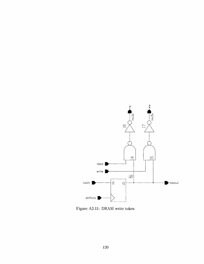
x x
LCn
read
write
tokin d q tokout
shiftclk
Figure A2.11: DRAM write token
120

d q 11
Figure A2.12: DRAM bitslice
out2 h.0 . ./ out1
phH1 2.8/0.35 2.8/0.35 phi2
gnd!
Figure A2.13: Phase measurement arbiter
121

49/0.5b 0.7/0.7
A Y
24.5/0.35
oe 24.5/0.35
Figure A2.14: Dram data 3-state driver
C (N0
0
:3:
2. 1/0.35 4.2/0.35
DataClockW - D
*-wotuFigure A2.15: Dram output data serializer
122


![DESIGN AND ANALYSIS OF EFFICIENT PHASE LOCKED LOOP … · Phase Locked Loop (PLL) mainly for synchronization, clock synthesis, skew and jitter reduction [5]. Phase locked loops find](https://static.fdocuments.in/doc/165x107/5e9d540ca2a49a4e746bfacd/design-and-analysis-of-efficient-phase-locked-loop-phase-locked-loop-pll-mainly.jpg)