Analog-to-Digital Converter (ADC) Introduction to Mechatronics Fall 2012 Craig Woodin Ali AlSaibie...
61
Analog-to-Digital Converter (ADC) Introduction to Mechatronics Fall 2012 Craig Woodin Ali AlSaibie Ehsan Maleki
-
Upload
josephine-bryan -
Category
Documents
-
view
219 -
download
1
Transcript of Analog-to-Digital Converter (ADC) Introduction to Mechatronics Fall 2012 Craig Woodin Ali AlSaibie...
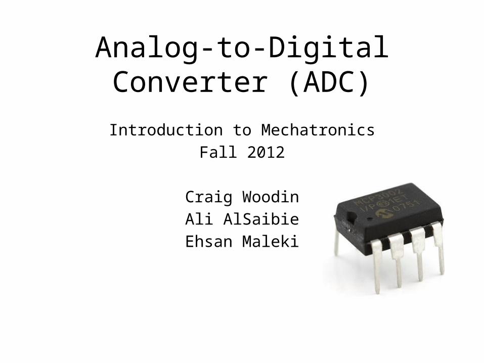
Analog-to-Digital Converter (ADC)
Introduction to MechatronicsFall 2012
Craig WoodinAli AlSaibie
Ehsan Maleki
Background Information
What is ADC?Conversion ProcessAccuracyExamples of ADC applications
Presenter: Craig Woodin

Signal Types
Analog Signals Any continuous signal that a
time varying variable of the signal is a representation of some other time varying quantity Measures one quantity in
terms of some other quantity Examples
• Speedometer needle as function of speed
• Radio volume as function of knob movement
t
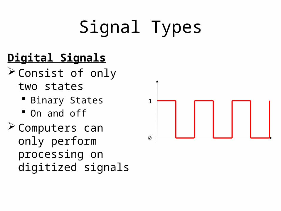
Signal Types
Digital Signals Consist of only two states
Binary States On and off
Computers can only perform processing on digitized signals 0
1
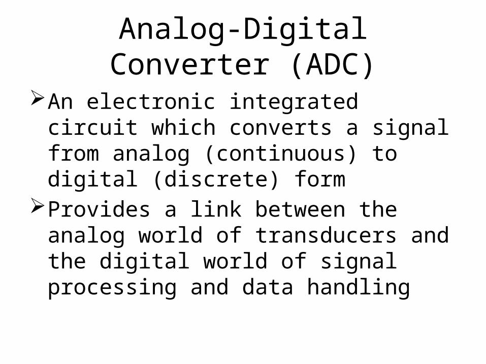
Analog-Digital Converter (ADC)
An electronic integrated circuit which converts a signal from analog (continuous) to digital (discrete) form
Provides a link between the analog world of transducers and the digital world of signal processing and data handling

Analog-Digital Converter (ADC)
An electronic integrated circuit which converts a signal from analog (continuous) to digital (discrete) form
Provides a link between the analog world of transducers and the digital world of signal processing and data handling
t

Analog-Digital Converter (ADC)
An electronic integrated circuit which converts a signal from analog (continuous) to digital (discrete) form
Provides a link between the analog world of transducers and the digital world of signal processing and data handling
t

ADC Conversion Process
Two main steps of process1. Sampling and Holding2. Quantization and Encoding
ttInput: Analog Signal
Sampling and Hold
Quantizingand
Encoding
Analog-to-Digital Converter

ADC Process
t
Continuous Signal
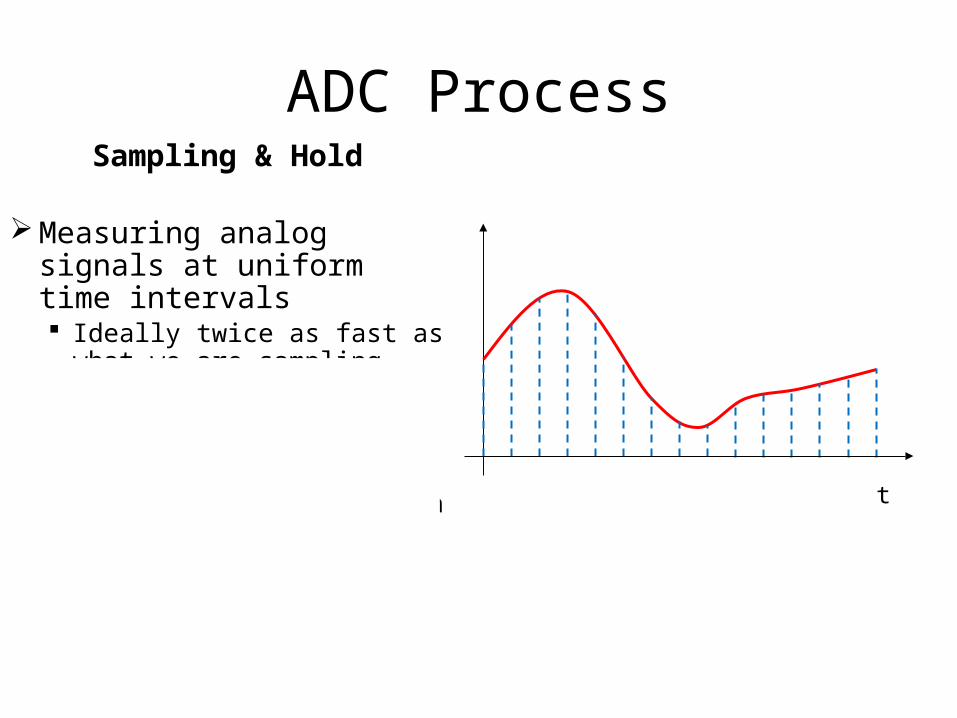
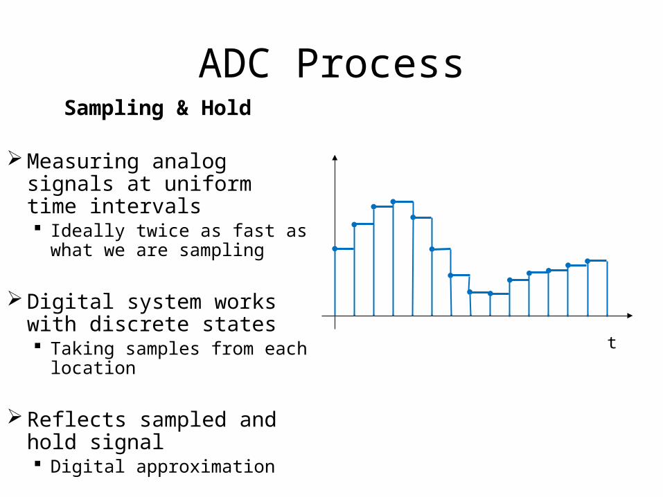
Sampling & Hold
Measuring analog signals at uniform time intervals Ideally twice as fast as what
we are sampling
Digital system works with discrete states Taking samples from each
location
Reflects sampled and hold signal Digital approximation
ADC Process
t
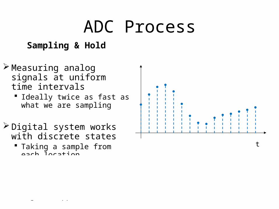
Sampling & Hold
Measuring analog signals at uniform time intervals Ideally twice as fast as what
we are sampling
Digital system works with discrete states Taking samples from each
location
Reflects sampled and hold signal Digital approximation
ADC Process
t
Sampling & Hold
Measuring analog signals at uniform time intervals Ideally twice as fast as what
we are sampling
Digital system works with discrete states Taking a sample from each
location
Reflects sampled and hold signal Digital approximation
ADC Process
t
Sampling & Hold
Measuring analog signals at uniform time intervals Ideally twice as fast as what
we are sampling
Digital system works with discrete states Taking samples from each
location
Reflects sampled and hold signal Digital approximation
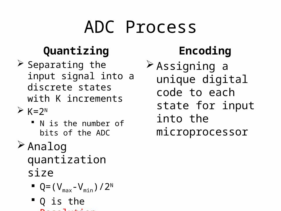
ADC ProcessQuantizing
Separating the input signal into a discrete states with K increments
K=2N
N is the number of bits of the ADC
Analog quantization size Q=(Vmax-Vmin)/2N
Q is the Resolution
Encoding Assigning a unique
digital code to each state for input into the microprocessor
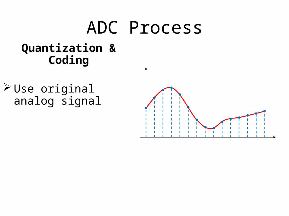
ADC ProcessQuantization & Coding
Use original analog signal

ADC ProcessQuantization & Coding
Use original analog signal
Apply 2 bit coding
K=22 00011011
00
11
10
01

ADC ProcessQuantization & Coding
Use original analog signal
Apply 2 bit coding
K=22 00011011
00
11
10
01
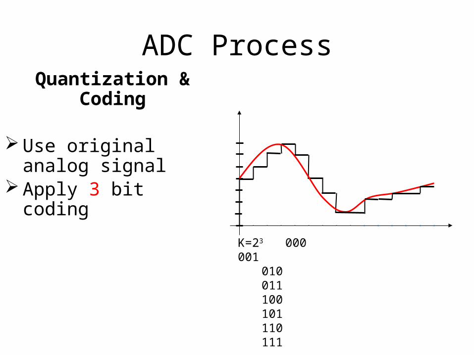
ADC ProcessQuantization & Coding
Use original analog signal
Apply 3 bit coding
K=23 000001010011100101110111
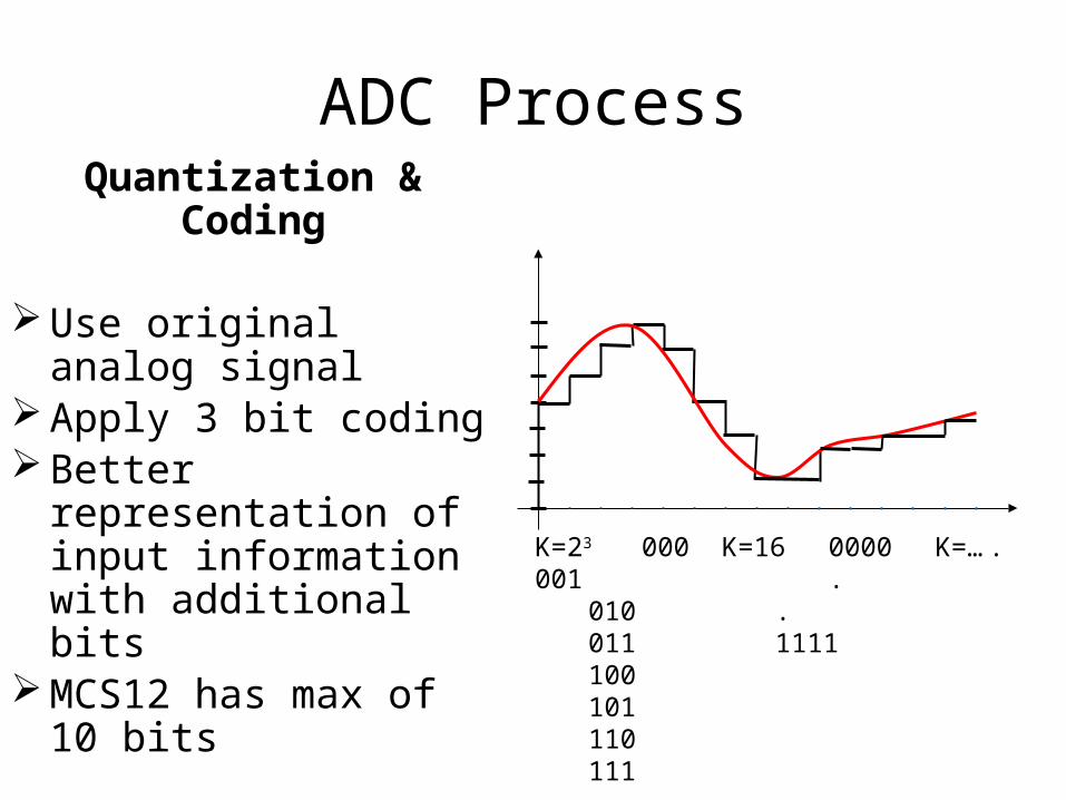
ADC ProcessQuantization & Coding
Use original analog signal
Apply 3 bit coding Better representation of
input information with additional bits
MCS12 has max of 10 bits
K=23 000001010011100101110111
K=16 0000 K=…...1111

ADC Process-Accuracy
Sampling Rate, Ts Based on number of steps
required in the conversion process
Increases the maximum frequency that can be measured
Resolution, Q Improves accuracy in
measuring amplitude of analog signal
Limited by the signal-to-noise ratio (~6dB)
t t
The accuracy of an ADC can be improved by increasing:

ADC Process-Accuracy
Sampling Rate, Ts Based on number of steps
required in the conversion process
Increases the maximum frequency that can be measured
Resolution (bit depth), Q Improves accuracy in
measuring amplitude of analog signal
t t
The accuracy of an ADC can be improved by increasing:

ADC-Error Possibilities
Aliasing (sampling) Occurs when the input signal is changing much faster
than the sample rate Should follow the Nyquist Rule when sampling
• Answers question of what sample rate is required• Use a sampling frequency at least twice as high as the
maximum frequency in the signal to avoid aliasing• fsample>2*fsignal
Quantization Error (resolution) Optimize resolution Dependent on ADC converter of microcontoller

ADC Applications
ADC are used virtually everywhere where an analog signal has to be processed, stored, or transported in digital form Microphones Strain Gages Thermocouple Digital Multimeters

Types of ADC
Successive Approximation A/D ConverterFlash A/D ConverterDual Slope A/D ConverterDelta-Sigma A/D Converter
Presenter: Ali AlSaibie
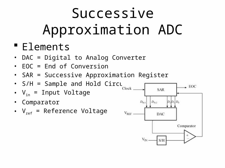
Successive Approximation ADC
Elements• DAC = Digital to Analog Converter• EOC = End of Conversion• SAR = Successive Approximation Register• S/H = Sample and Hold Circuit• Vin = Input Voltage• Comparator• Vref = Reference Voltage

Successive Approximation ADC
Algorithm• Uses an n-bit DAC and original analog results• Performs a binary comparison of VDAC and Vin
• MSB is initialized at 1 for DAC• If Vin < VDAC (VREF / 2^n=1) then MSB is reset to 0
• If Vin > VDAC (VREF / 2^n) Successive Bits set to 1 otherwise 0• Algorithm is repeated up to LSB• At end DAC in = ADC out • N-bit conversion requires N comparison cycles
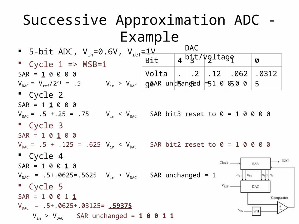
Successive Approximation ADC - Example 5-bit ADC, Vin=0.6V, Vref=1V Cycle 1 => MSB=1SAR = 1 0 0 0 0VDAC
= Vref/2^1 = .5 Vin > VDAC SAR unchanged = 1 0 0 0 0
Cycle 2SAR = 1 1 0 0 0VDAC
= .5 +.25 = .75 Vin < VDAC SAR bit3 reset to 0 = 1 0 0 0 0
Cycle 3SAR = 1 0 1 0 0VDAC
= .5 + .125 = .625 Vin < VDAC SAR bit2 reset to 0 = 1 0 0 0 0
Cycle 4SAR = 1 0 0 1 0VDAC
= .5+.0625=.5625 Vin > VDAC SAR unchanged = 1 0 0 1 0
Cycle 5SAR = 1 0 0 1 1VDAC
= .5+.0625+.03125= .59375
Vin > VDAC SAR unchanged = 1 0 0 1 1
Bit 4 3 2 1 0Voltage .5 .25 .125 .0625 .03125
DAC bit/voltage
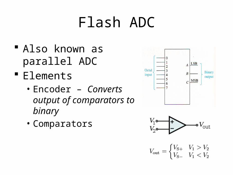
Flash ADC
Also known as parallel ADC Elements
• Encoder – Converts output of comparators to binary
• Comparators
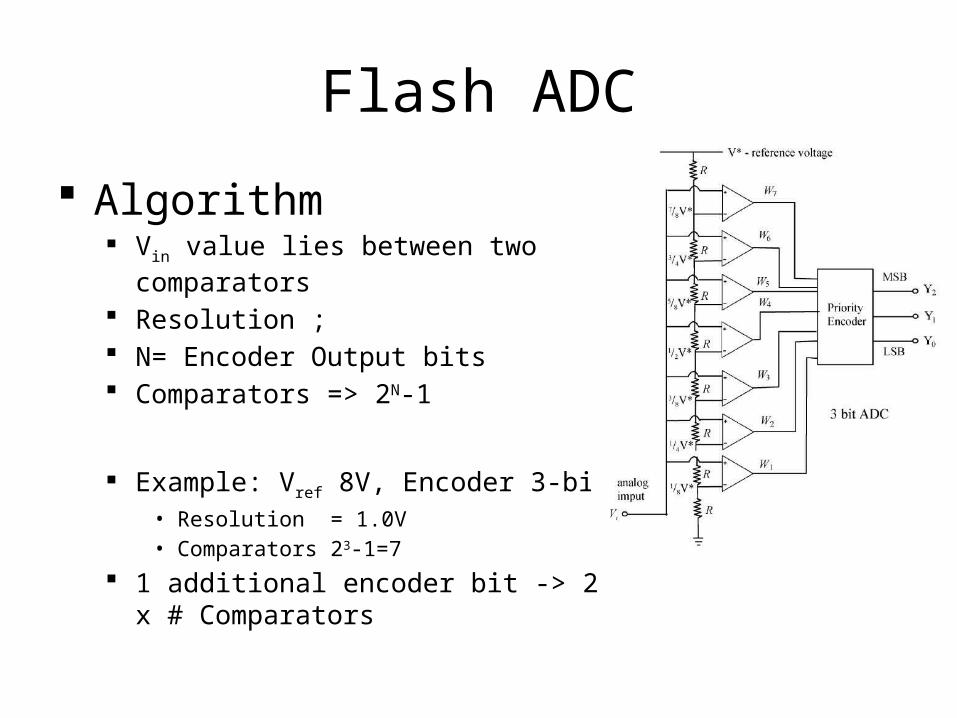
Flash ADC
Algorithm Vin value lies between two comparators Resolution ; N= Encoder Output bits Comparators => 2N-1
Example: Vref 8V, Encoder 3-bit• Resolution = 1.0V• Comparators 23-1=7
1 additional encoder bit -> 2 x # Comparators
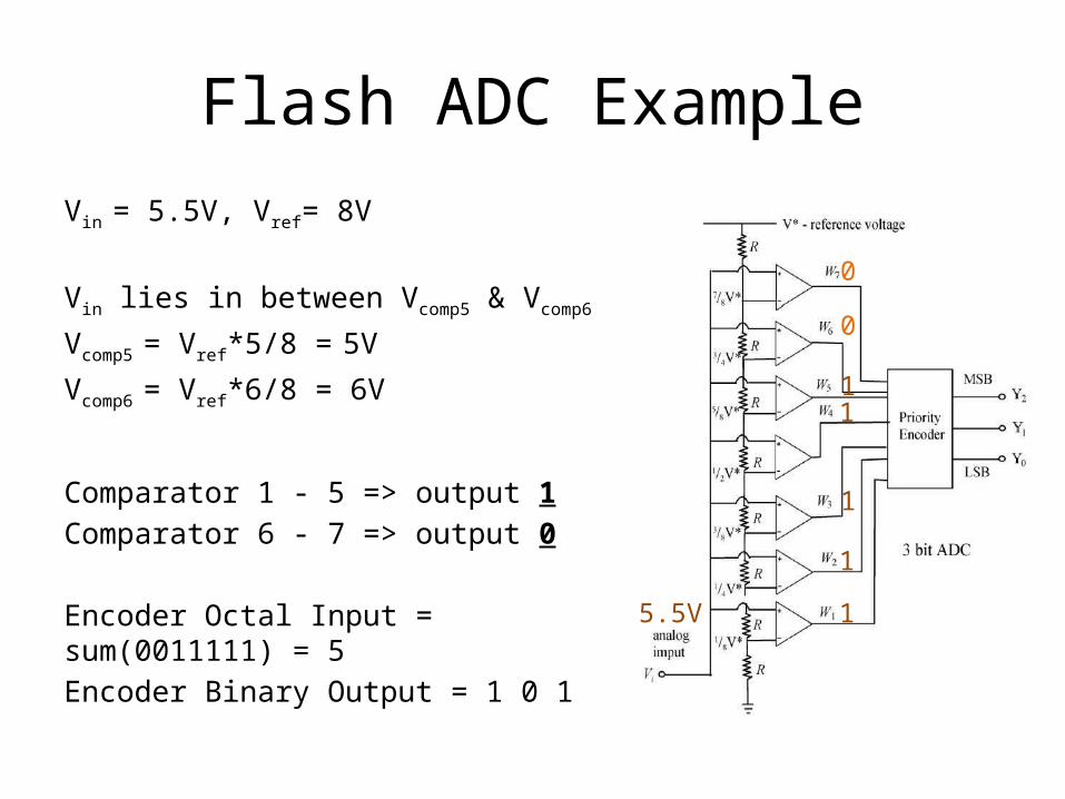
Flash ADC ExampleVin = 5.5V, Vref= 8V
Vin lies in between Vcomp5 & Vcomp6
Vcomp5 = Vref*5/8 = 5V
Vcomp6 = Vref*6/8 = 6V
Comparator 1 - 5 => output 1Comparator 6 - 7 => output 0
Encoder Octal Input = sum(0011111) = 5Encoder Binary Output = 1 0 1
5.5V 1
1
1
11
0
0
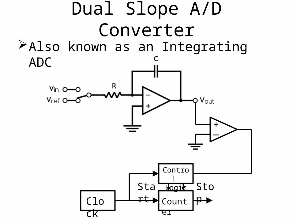
Dual Slope A/D ConverterAlso known as an Integrating ADC
Clock Counter
Control Logic
+_
Start Stop
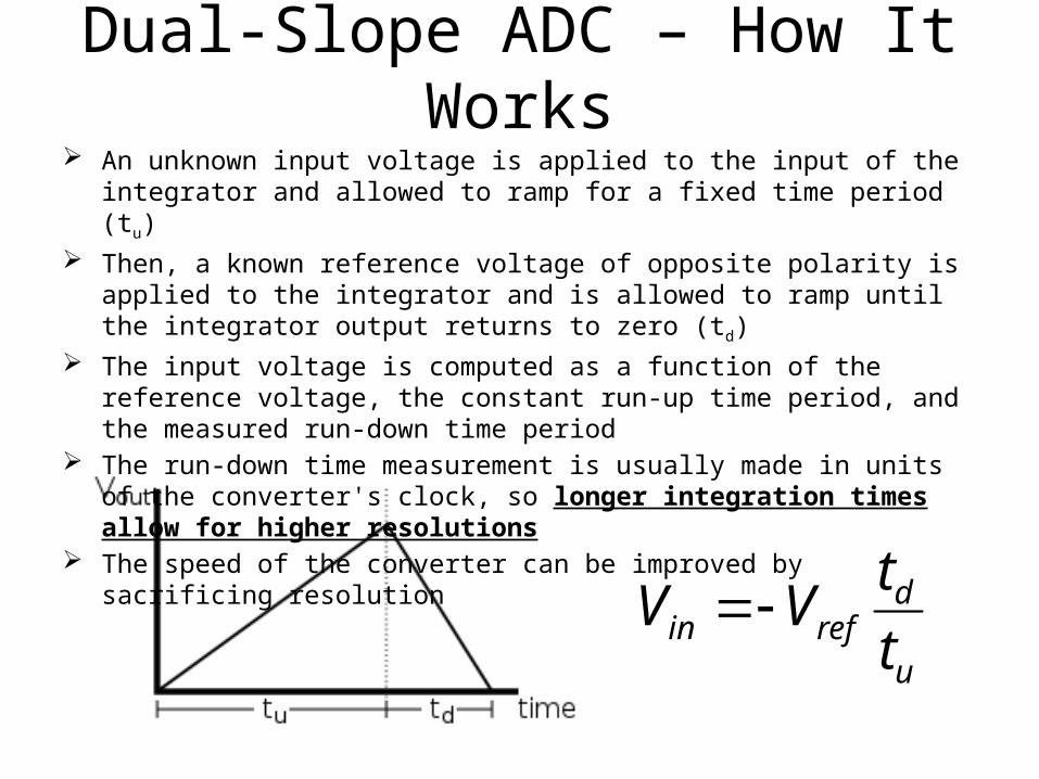
Dual-Slope ADC – How It Works
u
drefin t
tVV
An unknown input voltage is applied to the input of the integrator and allowed to ramp for a fixed time period (tu)
Then, a known reference voltage of opposite polarity is applied to the integrator and is allowed to ramp until the integrator output returns to zero (td)
The input voltage is computed as a function of the reference voltage, the constant run-up time period, and the measured run-down time period
The run-down time measurement is usually made in units of the converter's clock, so longer integration times allow for higher resolutions
The speed of the converter can be improved by sacrificing resolution
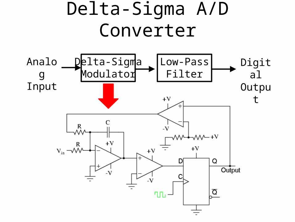
Delta-Sigma A/D Converter
Delta-Sigma Modulator
AnalogInput
DigitalOutput
Low-PassFilter
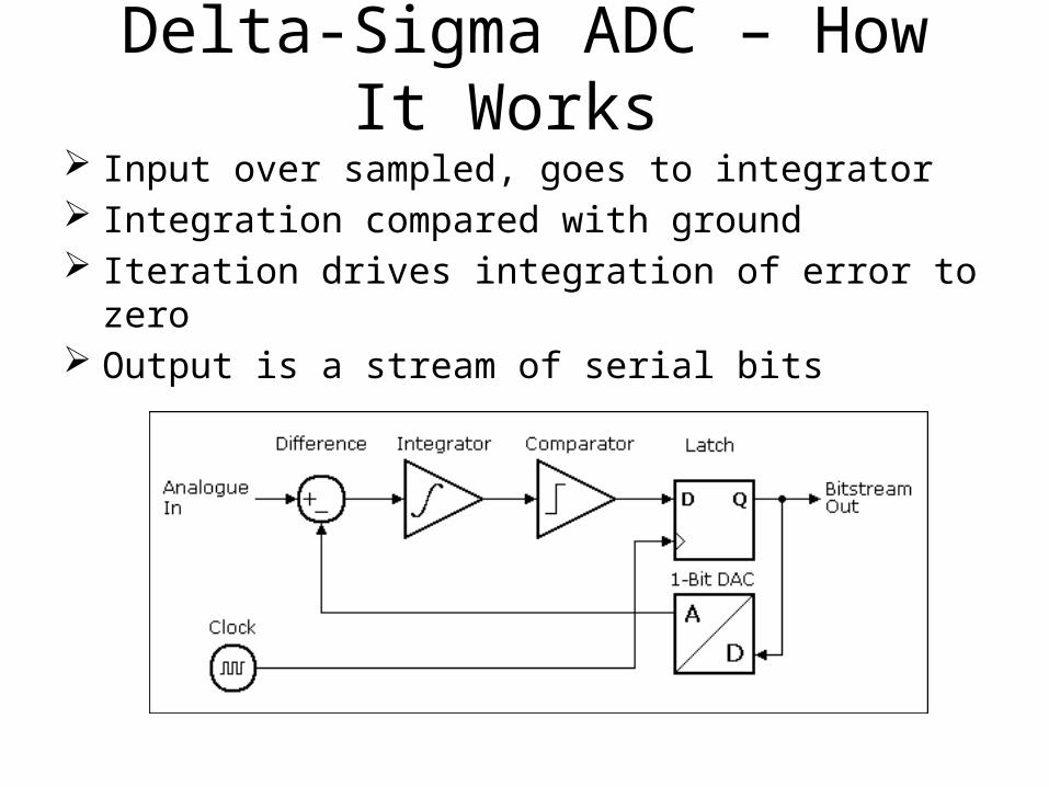
Delta-Sigma ADC – How It Works Input over sampled, goes to integrator Integration compared with ground Iteration drives integration of error to zero Output is a stream of serial bits

Comparison of ADC’s
Type Speed (relative)
Cost(relative)
Resolution(bits)
Dual Slope Slow Med 12-16
Flash Very Fast High 4-12
Successive Approx
Medium – Fast Low 8-16
Sigma – Delta Slow Low 12-24
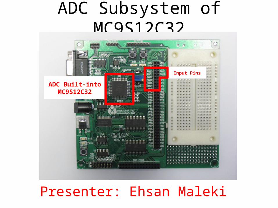
ADC Subsystem of MC9S12C32
Input PinsADC Built-into
MC9S12C32
Presenter: Ehsan Maleki

ADC - Schematic Diagram
ATD
Port AD

ATD 10B8C - Block Diagram
Analog InputGeneral Purpose I/O
External Trigger
Analog InputGeneral Purpose I/O
High/LowRef Voltage
Power Supplies
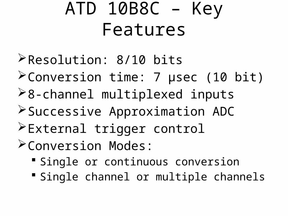
ATD 10B8C – Key Features
Resolution: 8/10 bitsConversion time: 7 μsec (10 bit)8-channel multiplexed inputsSuccessive Approximation ADCExternal trigger controlConversion Modes:
Single or continuous conversion Single channel or multiple channels
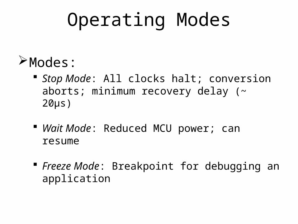
Operating Modes
Modes: Stop Mode: All clocks halt; conversion aborts; minimum
recovery delay (~ 20μs)
Wait Mode: Reduced MCU power; can resume
Freeze Mode: Breakpoint for debugging an application

Registers
MC9S12C Family Reference Manual: Ch. 8
REGISTERS 6 Control Registers (first 2 are reserved!) 2 Status Registers 2 Test Registers 1 Digital Input Enable Register 1 Digital Port Data Register 8 Result Registers
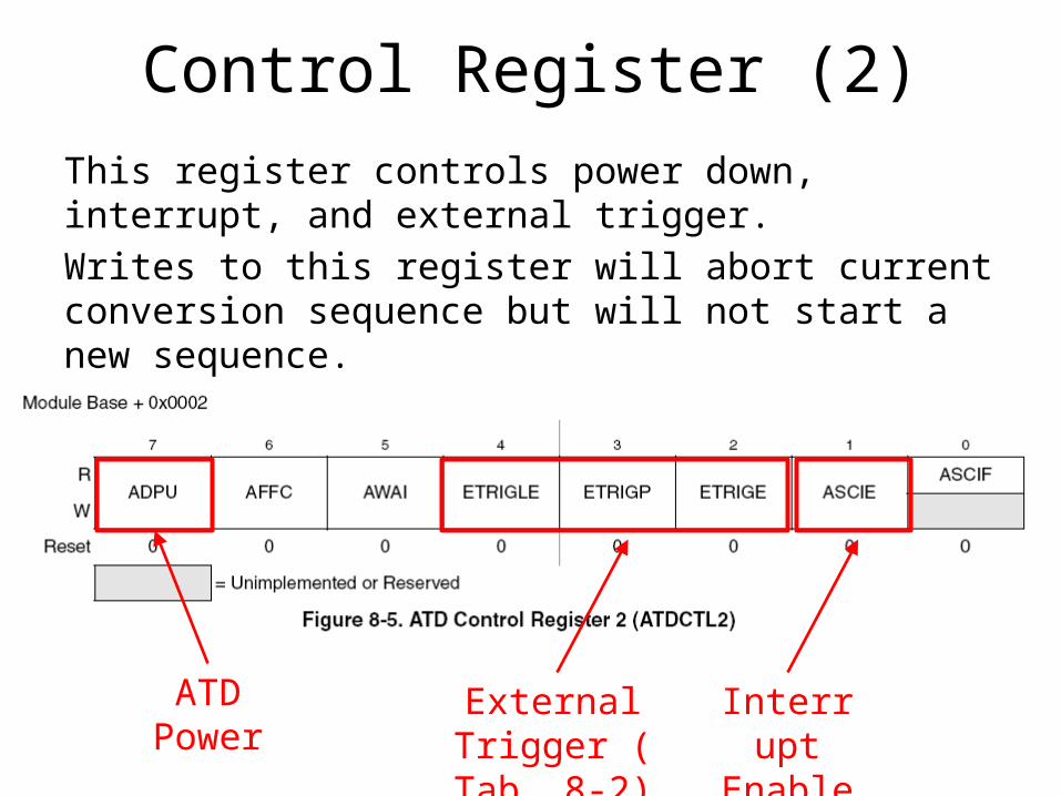
Control Register (2)This register controls power down, interrupt, and external trigger.Writes to this register will abort current conversion sequence but will not start a new sequence.
ATDPower
Interrupt Enable
External Trigger (Tab. 8-2)
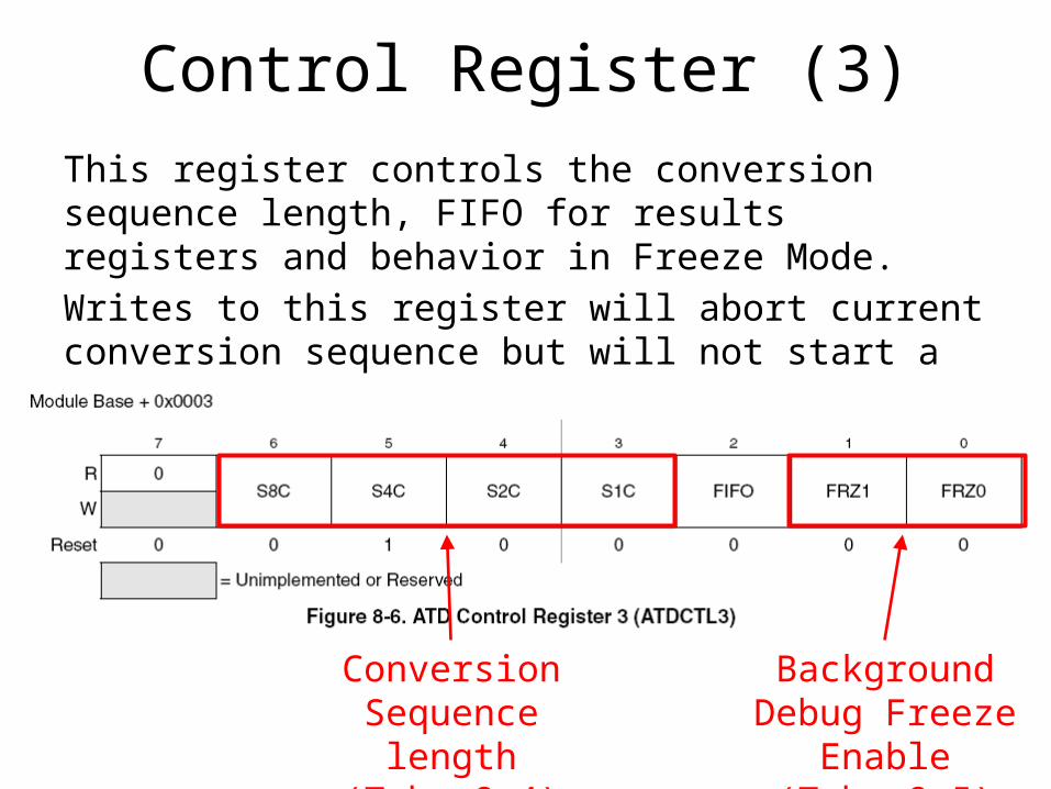
Control Register (3)This register controls the conversion sequence length, FIFO for results registers and behavior in Freeze Mode.Writes to this register will abort current conversion sequence but will not start a new sequence.
Conversion Sequence length
(Tab. 8-4)
Background Debug Freeze Enable
(Tab. 8-5)
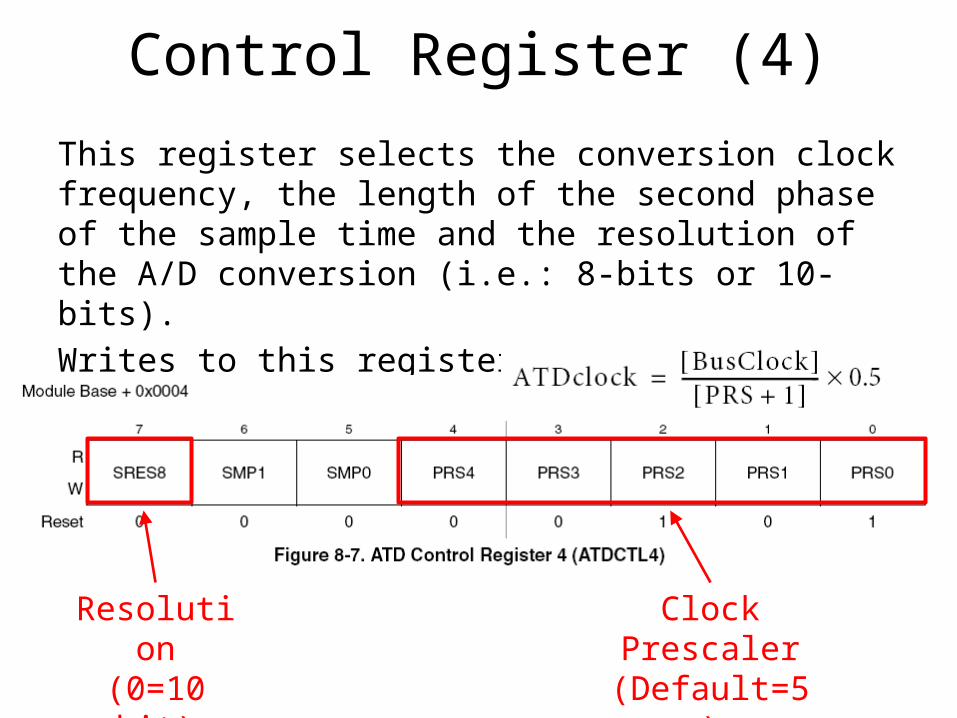
Control Register (4)
This register selects the conversion clock frequency, the length of the second phase of the sample time and the resolution of the A/D conversion (i.e.: 8-bits or 10-bits).Writes to this register will abort current conversion sequence but will not start a new sequence.
Resolution(0=10 bit)
Clock Prescaler(Default=5)(Tab. 8-8)

Control Register (5)This register selects the type of conversion sequence and the analog input channels sampled.Writes to this register will abort current conversion sequence and start a new conversion sequence.
Result Register Data Justification
RRD Unsigned (0) / Signed (1) (Tab. 8-10/11)
Single (0) / Continuous (1)Conversion Mode
Single (0) / Multi (1)Channel Mode
Analog Input Channel Select(Tab. 8-12)
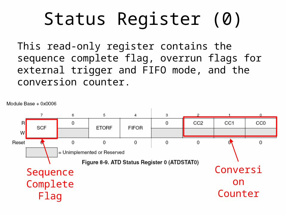
Status Register (0)This read-only register contains the sequence complete flag, overrun flags for external trigger and FIFO mode, and the conversion counter.
Sequence Complete Flag
ConversionCounter

Status Register (1)
This read-only register contains the Conversion Complete Flags.
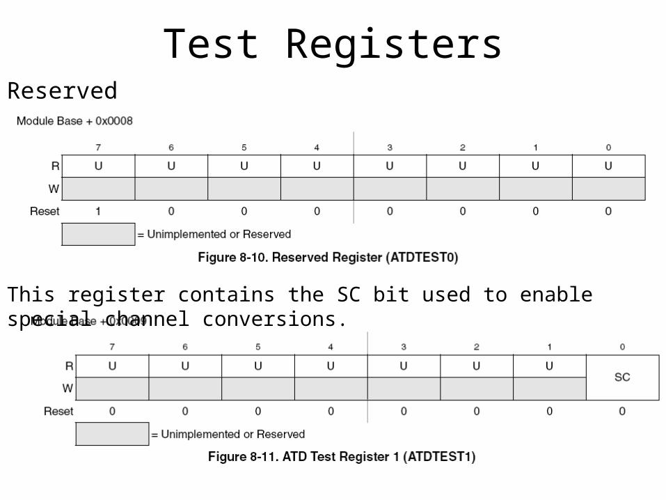
Test RegistersReserved
This register contains the SC bit used to enable special channel conversions.
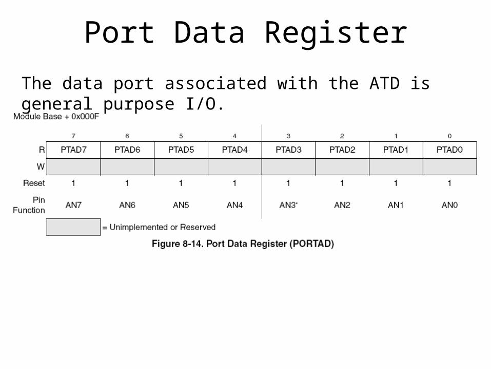
Port Data Register
The data port associated with the ATD is general purpose I/O.
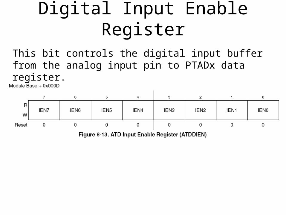
Digital Input Enable Register
This bit controls the digital input buffer from the analog input pin to PTADx data register.
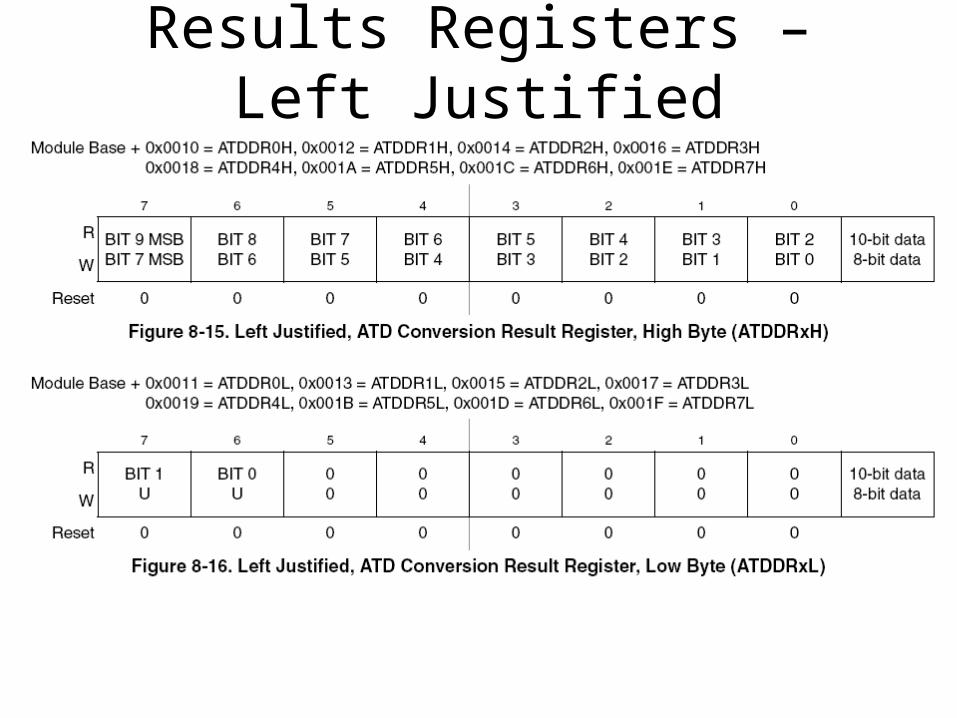
Results Registers – Left Justified

Results Registers – Right Justified
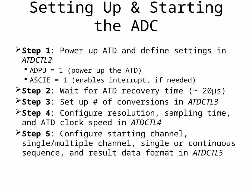
Step 1: Power up ATD and define settings in ATDCTL2 ADPU = 1 (power up the ATD) ASCIE = 1 (enables interrupt, if needed)
Step 2: Wait for ATD recovery time (~ 20μs) Step 3: Set up # of conversions in ATDCTL3 Step 4: Configure resolution, sampling time, and ATD
clock speed in ATDCTL4 Step 5: Configure starting channel, single/multiple
channel, single or continuous sequence, and result data format in ATDCTL5
Setting Up & Starting the ADC

QUESTIONS?

Appendix
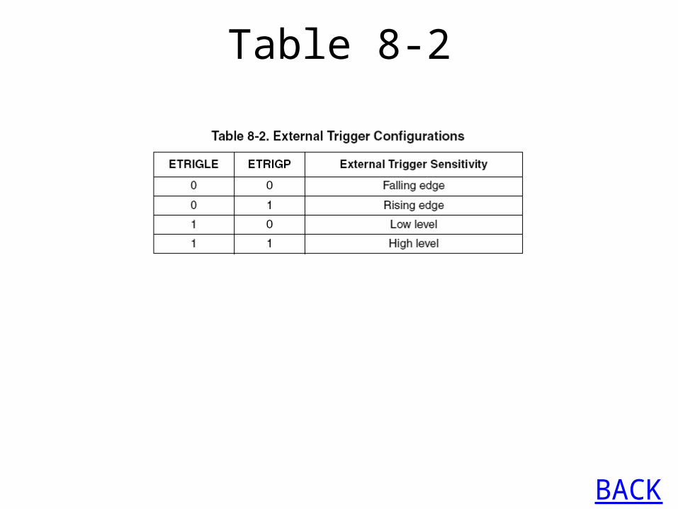
Table 8-2
BACK
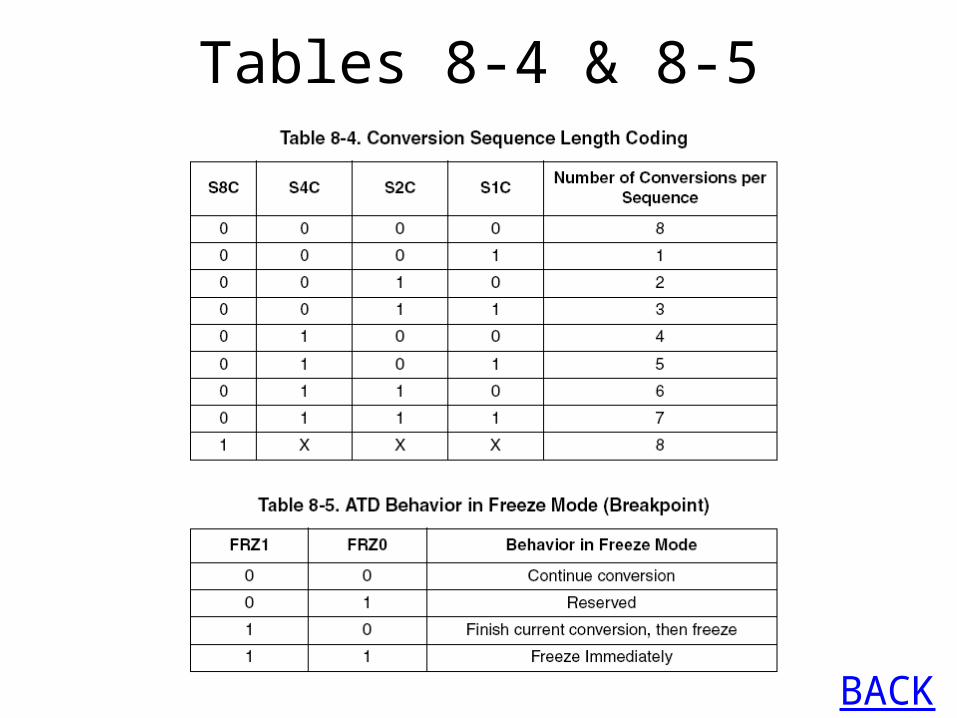
Tables 8-4 & 8-5
BACK
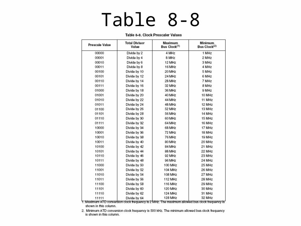
Table 8-8
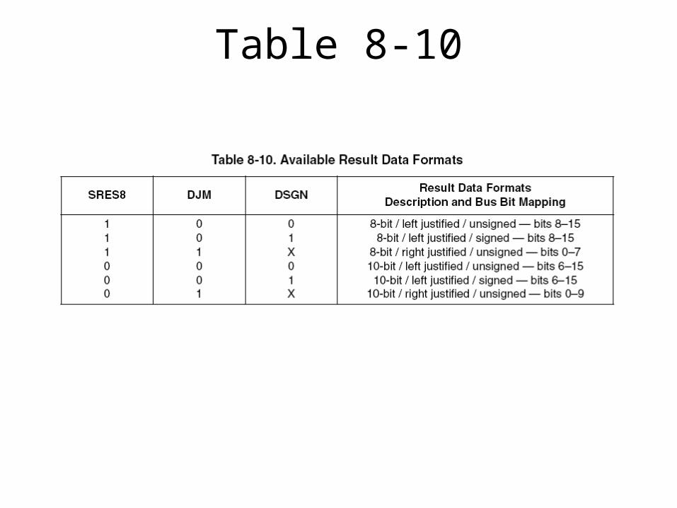
Table 8-10
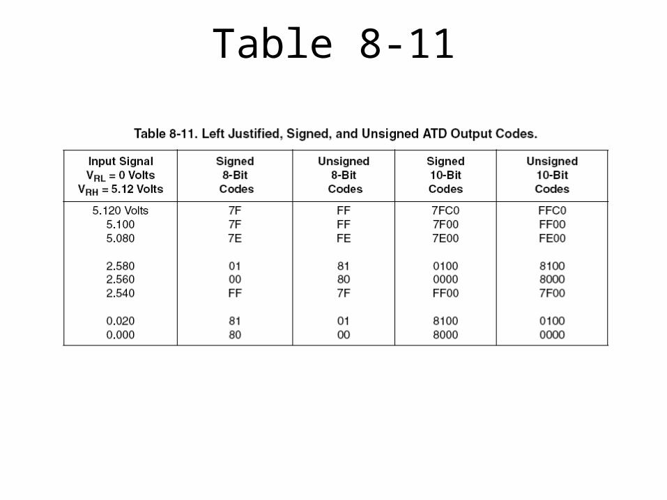
Table 8-11
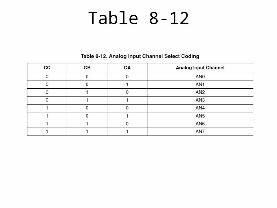
Table 8-12

References http://en.wikipedia.org/wiki/Analog-to-digital_converter http://
www.grin.com/object/external_document.259394/fb1fe2e3b955672eca3458c9116d595b_LARGE.png
http://en.wikipedia.org/wiki/Successive_approximation_ADC http://www.maximintegrated.com/app-notes/index.mvp/id/810 http://en.wikipedia.org/wiki/Delta-sigma_modulation http://www.beis.de/Elektronik/DeltaSigma/DeltaSigma.html http://www.allaboutcircuits.com/vol_4/chpt_13/9.html http://en.wikipedia.org/wiki/Integrating_ADC MC9S12C Family Reference Manual