Analog to Digital Conversion - University of North …jmconrad/ECGR4161-2011-05/...ADC - Successive...
21
Analog to Digital Conversion 1
Transcript of Analog to Digital Conversion - University of North …jmconrad/ECGR4161-2011-05/...ADC - Successive...

Analog to Digital Conversion
1

Why It’s Needed
Embedded systems often need to measure values of physical parametersThese parameters are usually continuous (analog) and not in a digital form
which computers (which operate on discrete data values) can process
• Pressure– Blood pressure monitor– Altimeter– Car engine controller– Scuba dive computer – Tsunami detector
• Temperature– Thermometer (do you have a fever?)– Thermostat for building, fridge, freezer– Car engine controller– Chemical reaction monitor– Safety (e.g. microprocessor processor
– Tsunami detector
• Acceleration– Air bag controller– Vehicle stability– Video game remote
• Mechanical strain• Other
– Touch screen controller– EKG, EEG– Breathalyzer
– Safety (e.g. microprocessor processor thermal management)
• Light (or infrared or ultraviolet) intensity
– Digital camera– IR remote control receiver– Tanning bed– UV monitor
• Rotary position– Wind gauge– Knobs

The Big Picture
PressureSensor
Analog to Digital
Converter
// Your softwareADC_Code = ad0;V_sensor = ADC_code*V_ref/1023;Pressure_kPa = 250 * (V_sensor/V_supply+0.04);Depth_ft = 33 * (Pressure_kPa – Atmos_Press_kPa)/101.3;
V_sensor ADC_Code
V_ref
Voltages
V_ref
ADC Output Codes
111..111111..110111..101111..100
AirPressure
V_sensor ADC_Code
Ground 000..000000..001
1. Sensor detects air pressure and generates a proportional output voltageV_sensor
2. ADC generates a proportional digital integer (code) based on V_sensor and V_ref
3. Code can convert that integer to a something more useful
1. first a float representing the voltage, 2. then another float representing pressure,3. finally another float representing depth

Getting From Analog to Digital
A Comparator is a circuit which compares an analog input voltage with a reference voltage and determines which is larger, returning a 1-bit number
An Analog to Digital converter [AD or ADC] is a circuit which accepts an analog input signal (usually a voltage) and produces a corresponding multi-bit number at the output.
0
1
0
1
Vin
Vref
Clock
0Vin0
Vin1
ComparatorComparatorComparatorComparator A/D ConverterA/D ConverterA/D ConverterA/D Converter

Waveform Sampling and Quantization
A waveform is sampled at a constant rate – every ∆t
– Each such sample represents the instantaneous amplitude at the instant
time
Dig
ital v
alue
– Each such sample represents the instantaneous amplitude at the instant of sampling
– “At 37 ms, the input is 1.91341914513451451234311… V”– Sampling converts a continuous time signal to a discrete time signal
The sample can now be quantized (converted) into a digital value– Quantization represents a continuous (analog) value with the closest
discrete (digital) value– “The sampled input voltage of 1.91341914513451451234311… V is best
represented by the code 0x018, since it is in the range of 1.901 to 1.9980 V which corresponds to code 0x018.”
Transfer Function
The ADC produces a given output code for all voltages within a specific rangeThe ideal transfer function A/D converter is a stair-step function.
Consider a 2-bit ADC– 0 to 4 V input– LSB = 4/22 = 1 V 10
11
Out
put C
ode
1 LSB
“2.0 V”
“3.0 V”
– LSB = 4/2 = 1 V
Red line– Truncation– Maximum error is -1 LSB or +
0 LSB
Blue line– Rounding– Maximum error in conversion
is usually ± 1/2 bit.– Half as much error if we limit
range to Vref(1-2N/2)
Input Voltage
00
10
Out
put C
ode
2.0
V
3.0
V
4.0
V
01
1.0
V
“2.0 V”
“0.0 V”
“1.0 V”

Transfer Function Equation
General Equationn = converted codeVin = sampled input voltageV+ref = upper end of input voltage
rangeV-ref = lower end of input voltage rangeN = number of bits of resolution in
( )2/1
2
+=+ref
Nin
V
Vn
230.3 10
=+= v
Simplification with V-ref = 0 V
N = number of bits of resolution in ADC
( )2/1
2
+−
−=
−+
−
refref
Nrefin
VV
VVn
6762/15
230.3 10
=
+=vv
n
floor function: nearest integer I such that I <= XX = I

Example
Your voltage range is 3.3 to 0 V, device is an 8-bit ADCa) What is the step size?b) If vin is 0.9v, what is n?
Embedded Systems 8
( )2/1
2
+−
−=
−+
−
refref
Nrefin
VV
VVn

A/D – Flash ConversionA multi-level voltage divider is used to set voltage levels over the complete range of conversion.A comparator is used at each level to determine whether the voltage is lower or higher than the level.The series of comparator outputs are encoded to a binary number in digital logic (a priority encoder)Components used 4/8 V
5/8 V
6/8 V
7/8 V +
-
+
-
+
-
1V ComparatorsR
R
R
R
1
1
1Components used
– 2N resistors– 2N-1 comparators
Note – This particular resistor divider
generates voltages which are not offset by ½ bit, so maximum error is 1 bit
– We could change this offset voltage by using resistors of values R, 2R, 2R ... 2R, 3R (starting at bottom)
1/8 V
2/8 V
3/8 V
4/8 V
Encoder+
-
+
-
+
-
+
-
Vin
R
R
R
R
3
0
0
0
0

ADC - Dual Slope Integrating
Operation• Input signal is integrated for a fixed
time• Input is switched to the negative
reference and the negative reference is then integrated until the integrator output is zero
• The time required to integrate the signal back to zero is used to signal back to zero is used to compute the value of the signal
• Accuracy dependent on Vref and timing
Characteristics• Noise tolerant (Integrates
variations in the input signal during the T1 phase)
• Typically slow conversion rates (Hz to few kHz)
∫∫ −=21
00
11T
ref
T
in dtVC
dtVC
1
2
T
TVV refin =
Slope proportionalto input voltage

ADC - Dual Slope Integrating
Analog Input (Va)
+
-+
--Vreference
Comparator
Integrator
Control Logic
Counter
Start of ConversionStatus
Clock
Digital Output 12
Comparator output

ADC - Successive Approximation Conversion
Successively approximate input voltage by using a binary search and a DACSA Register holds current approximation of resultSet all DAC input bits to 0Start with DAC’s most significant bit V
olta
ge
Test voltage(DAC output)
111111
100000
100100
AnalogInput
0000
100110
0000
0
000 00
0 1
bitRepeat
– Set next input bit for DAC to 1– Wait for DAC and comparator
to stabilize– If the DAC output (test voltage)
is smaller than the input then set the current bit to 1, else clear the current bit to 0
Vol
tage
TimeStart of Conversion
T1 T2 T3 T4 T5 T6000000kn
ow 1
xxxx
x, tr
y 11
0000
know
xxx
xxx,
try
100
000
know
10x
xxx,
try
101
000
know
100
xxx,
try
1001
00
know
100
1xx,
try
1001
10
know
100
11x,
try
1001
11
know
100
110.
Don
e.

A/D - Successive Approximation
Converter Schematic
Analog Input +
-
Comparator outputConverter Schematic
D/A Converter
SuccessiveApproximation
RegisterStart of ConversionStatus
Clock
Digital Output 12

ADC Performance Metrics
Linearity measures how well the transition voltages lie on a straight line.
Differential linearity measure the equality of the step size.
Conversion time:between start of conversion and generation of resultof result
Conversion rate = inverse of conversion time

Sampling Problems
Nyquist criterion– Fsample >= 2 * Fmax frequency component– Frequency components above ½ Fsample are aliased, distort
measured signal
Nyquist and the real world– This theorem assumes we have a perfect filter with “brick wall” roll-
off– Real world filters have more gentle roll-off– Real world filters have more gentle roll-off– Inexpensive filters are even worse (e.g. first order filter is 20
dB/decade, aka 6 dB/octave)– So we have to choose a sampling frequency high enough that our
filter attenuates aliasing components adequately
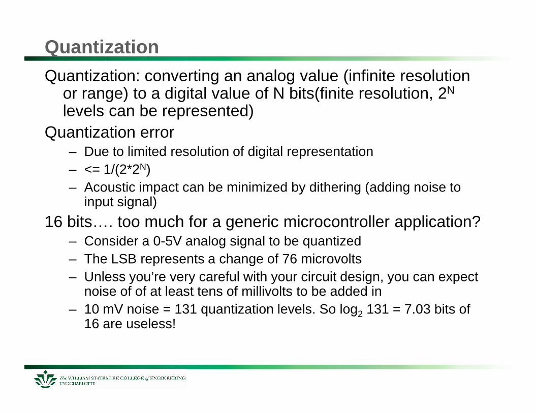
QuantizationQuantization: converting an analog value (infinite resolution
or range) to a digital value of N bits(finite resolution, 2N
levels can be represented)Quantization error
– Due to limited resolution of digital representation– <= 1/(2*2N)– Acoustic impact can be minimized by dithering (adding noise to
input signal)input signal)
16 bits…. too much for a generic microcontroller application?– Consider a 0-5V analog signal to be quantized– The LSB represents a change of 76 microvolts– Unless you’re very careful with your circuit design, you can expect
noise of of at least tens of millivolts to be added in– 10 mV noise = 131 quantization levels. So log2 131 = 7.03 bits of
16 are useless!

Inputs
Multiplexing– Typically share a single ADC among multiple inputs– Need to select an input, allow time to settle before sampling
Signal ConditioningSignal Conditioning– Amplify and filter input signal– Protect against out-of-range inputs with clamping diodes

Sample and Hold Devices
Some A/D converters require the input analog signal to be held constant during conversion, (eg. successive approximation devices)In other cases, peak capture or sampling at a specific point in
Analog InputSignal
Samplingswitch
HoldCapacitor
OutputSignal
sampling at a specific point in time necessitates a sampling device.This function is accomplished by a sample and hold device as shown to the right:These devices are incorporated into some A/D converters

M30626 A/D Converter Overview

M30262 Converter Overview (626P similar)
Embedded Systems 8-20

Digital to Analog Conversion
May need to generate an analog voltage or current as an output signal– Audio, motor speed control, LED brightness, etc.
Digital to Analog Converter equation– n = input code– N = number of bits of resolution of converter– Vref = reference voltage– Vout = output voltage– V = V * n/(2N)– Vout = Vref * n/(2N)
0
1
0
1
Vout
Vref
D/A ConverterD/A ConverterD/A ConverterD/A Converter