Analog PWM Dimming in White-LED Drivers - Analog, … · · 2016-12-21driver devices. PWM dimming...
14
1 SNVA768 – December 2016 Submit Documentation Feedback Copyright © 2016, Texas Instruments Incorporated Analog PWM Dimming in White-LED Drivers Application Report SNVA768 – December 2016 Analog PWM Dimming in White-LED Drivers Travis Eichhorn ABSTRACT Pulse-width modulation (PWM) is a common type of dimming used to adjust the current in white-LED driver devices. PWM dimming takes a rectangle waveform with variable positive duty cycle (D) and adjusts the LED current proportionally. For many smaller format white LED drivers (7-inch screen size or smaller), the PWM signal is converted to a DC control voltage and made to drive the LED current in a DC (or analog) method. This application note discusses some of the benefits and drawbacks of a PWM-to-analog dimming method. Contents 1 PWM Dimming ............................................................................................................... 2 2 PWM-to-Analog Methods ................................................................................................... 2 List of Figures 1 LED Driver With Low-Pass-Filtered PWM Input ......................................................................... 3 2 TPS61165 (Low-Pass-Filtered PWM) Waveforms ...................................................................... 4 3 Offset Error in Feedback Voltage.......................................................................................... 4 4 Low-Pass-Filtered Current Response vs Duty Cycle ................................................................... 5 5 Sampled PWM-to-Analog Block Diagram ................................................................................ 6 6 Sampled PWM Current Response vs Duty Cycle ....................................................................... 7 7 PWM Sample Rate Options (LM36923x Devices) ...................................................................... 8 8 Determining PWM Hysteresis Based on Jitter ........................................................................... 9 9 LED Current-Mapping-Mode Options.................................................................................... 10 10 LED Current Ramping With Duty Cycle Changes ..................................................................... 11 11 Increasing PWM Resolution With Automatic Ramping ................................................................ 12 List of Tables 1 White LED Drivers with Low-Pass-Filtered, PWM-to-Analog Dimming............................................... 5 2 White LED Drivers With Sampled PWM-to-Analog Dimming .......................................................... 7 3 Programmable Sample Frequencies (LM3692x Devices) .............................................................. 8 4 Programmable Hysteresis Options (LM3692x Devices) ................................................................ 9 5 Devices With Ramping Between PWM Duty Cycle Changes ........................................................ 13 Trademarks All trademarks are the property of their respective owners.
Transcript of Analog PWM Dimming in White-LED Drivers - Analog, … · · 2016-12-21driver devices. PWM dimming...

1SNVA768–December 2016Submit Documentation Feedback
Copyright © 2016, Texas Instruments Incorporated
Analog PWM Dimming in White-LED Drivers
Application ReportSNVA768–December 2016
Analog PWM Dimming in White-LED Drivers
TravisEichhorn
ABSTRACTPulse-width modulation (PWM) is a common type of dimming used to adjust the current in white-LEDdriver devices. PWM dimming takes a rectangle waveform with variable positive duty cycle (D) and adjuststhe LED current proportionally. For many smaller format white LED drivers (7-inch screen size or smaller),the PWM signal is converted to a DC control voltage and made to drive the LED current in a DC (oranalog) method. This application note discusses some of the benefits and drawbacks of a PWM-to-analogdimming method.
Contents1 PWM Dimming ............................................................................................................... 22 PWM-to-Analog Methods ................................................................................................... 2
List of Figures
1 LED Driver With Low-Pass-Filtered PWM Input ......................................................................... 32 TPS61165 (Low-Pass-Filtered PWM) Waveforms ...................................................................... 43 Offset Error in Feedback Voltage.......................................................................................... 44 Low-Pass-Filtered Current Response vs Duty Cycle ................................................................... 55 Sampled PWM-to-Analog Block Diagram ................................................................................ 66 Sampled PWM Current Response vs Duty Cycle ....................................................................... 77 PWM Sample Rate Options (LM36923x Devices) ...................................................................... 88 Determining PWM Hysteresis Based on Jitter ........................................................................... 99 LED Current-Mapping-Mode Options.................................................................................... 1010 LED Current Ramping With Duty Cycle Changes ..................................................................... 1111 Increasing PWM Resolution With Automatic Ramping................................................................ 12
List of Tables
1 White LED Drivers with Low-Pass-Filtered, PWM-to-Analog Dimming............................................... 52 White LED Drivers With Sampled PWM-to-Analog Dimming .......................................................... 73 Programmable Sample Frequencies (LM3692x Devices).............................................................. 84 Programmable Hysteresis Options (LM3692x Devices) ................................................................ 95 Devices With Ramping Between PWM Duty Cycle Changes ........................................................ 13
TrademarksAll trademarks are the property of their respective owners.

PWM Dimming www.ti.com
2 SNVA768–December 2016Submit Documentation Feedback
Copyright © 2016, Texas Instruments Incorporated
Analog PWM Dimming in White-LED Drivers
1 PWM DimmingPWM dimming can be grouped into two major categories:• True PWM• Analog PWM
1.1 True PWM DimmingIn true PWM dimming the LED current is turned on/off at the programmed duty cycle and frequency. Thefrequency can be the same as the input PWM signal (direct PWM), or can be at a different frequency(indirect PWM). True PWM has been, for a long time, considered better in preserving the white point ofthe LED light output. The argument is made that because the peak current is the same across the entiredimming range, the white point vs current will be unchanged. This has largely been deemed as not trulyan issue, and in fact most (if not all) smart phones have adopted either a PWM-to-analog control or anI2C-to-analog control.
Although the white-point shift may or may not be an issue, true PWM does hold a couple definiteadvantages. First, offset errors at low currents are largely avoided because the LED current is turnedon/off at the maximum current. This allows for the reference voltage to maintain a high level, well aboveany offset induced errors. Secondly, LED brightness at very low DC current can have large errors in lightoutput. These errors can occur when the LED is biased at < 0.1% of its rated current. True PWM avoidsthis because the LED current is constant and near a high level at all brightness levels.
1.2 Analog PWM DimmingAnalog PWM dimming takes the PWM input and converts it to an analog control signal. This analogcontrol signal is used to adjust the voltage reference, which then sets the DC LED current (either acrossan external feedback resistor, or in a regulated current sink). The primary benefit of PWM-to-analogdimming is its low noise operation. Because the LED current is always continuous at the output, it isessentially noise free. This eliminates any acoustic noise generated due to large voltage fluctuationsacross ceramic output capacitors.
Another benefit with PWM-to-analog dimming is the better efficiency vs load current. In true PWMdimming, when the LED current is on, the switch and inductor are always conducting the maximum loadcurrent. This forces the maximum possible I2R losses in the resistive elements (inductor, switch, diode) ofthe circuit. In the PWM-to-analog dimming driver, the lower brightness levels always force lowerconduction losses. For example, consider a true PWM driver with 400-mA peak inductor current operatingat 50% duty cycle. The power loss in a 0.3-Ω inductor is (PL = 400 mA × 400 mA × 0.3 Ω × 0.5 = 24 mW).Compare this to a PWM-to-analog driver with the same average load (PL = 200 mA × 200 mA × 0.3 Ω =12 mW). In reality the PWM-to-analog driver would be even lower considering the lower VOUT and theelimination of added losses required to slew the LED current on/off that exist in the true PWM driver.
2 PWM-to-Analog MethodsTwo primary methods are used to convert the PWM input signal to an analog control voltage. The firstmethod uses a low-pass filter (LPF). This can be integrated into the device (typical) or can exist as anexternal filter capacitor. Once filtered the analog signal is used to drive the error amplifier (or current sink).
The second method uses a PWM sampler. Here the PWM input is continuously sampled and convertedinto a digital code, which is fed into a digital-to-analog converter (DAC) and then used to drive the erroramplifier (or current sink).
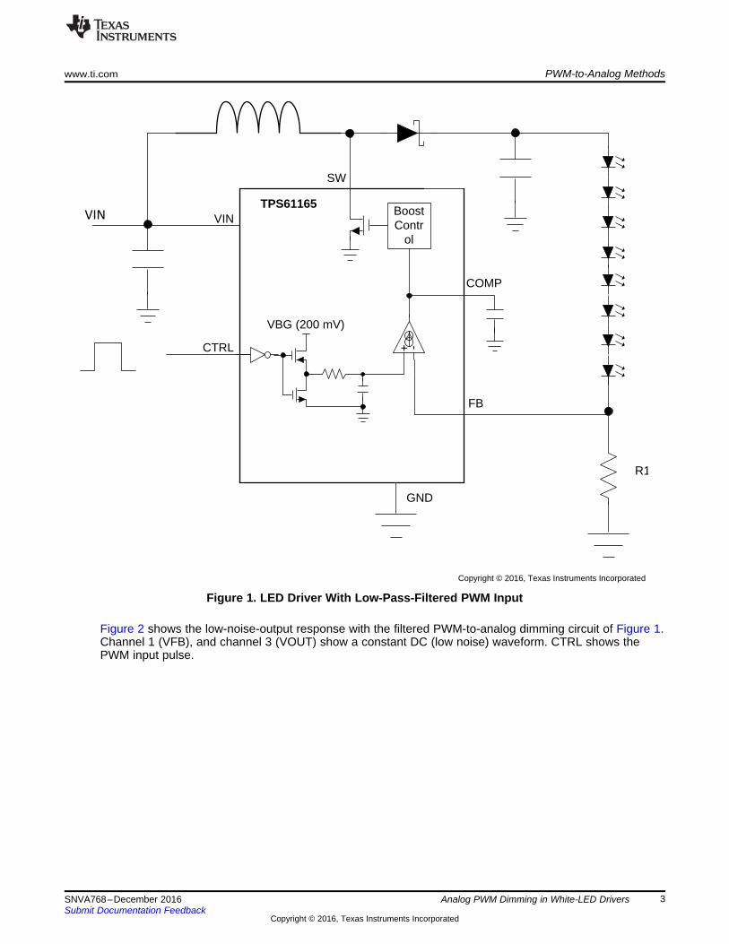
2.1 Low-Pass FilterAdding a low-pass filter in line with the PWM input is the simpler of the two PWM-to-analog dimmingmethods. An integrated filter turns the PWM input into a DC reference voltage, which is then used to setthe voltage at the boost FB pin, (or used to adjust the current in an integrated current sink). Figure 1shows a typical LED driver incorporating an LPF in a boost white-LED drive incorporating an externalRSET. The logic level PWM signal is buffered and level shifted so it swings between the reference voltage(VBG) and GND. The filtered signal is then used as the reference for the boost error amplifier, forcing theFB node to regulate to VREF in order to set the LED current across the low side resistor R1.
CTRL
VIN
SW
FB
GND
TPS61165VIN
R1
COMP
VBG (200 mV)+ -
BoostContr
ol
Copyright © 2016, Texas Instruments Incorporated
www.ti.com PWM-to-Analog Methods
3SNVA768–December 2016Submit Documentation Feedback
Copyright © 2016, Texas Instruments Incorporated
Analog PWM Dimming in White-LED Drivers
Figure 1. LED Driver With Low-Pass-Filtered PWM Input
Figure 2 shows the low-noise-output response with the filtered PWM-to-analog dimming circuit of Figure 1.Channel 1 (VFB), and channel 3 (VOUT) show a constant DC (low noise) waveform. CTRL shows thePWM input pulse.

+ -
CTRL
VBG (200mV)
ILED = VFB/RSET
VOS
FB
RSET
VFB = (VBG × D + VOS)
VFB
Input
Current
VOUT
CTRL
PWM-to-Analog Methods www.ti.com
4 SNVA768–December 2016Submit Documentation Feedback
Copyright © 2016, Texas Instruments Incorporated
Analog PWM Dimming in White-LED Drivers
Figure 2. TPS61165 (Low-Pass-Filtered PWM) Waveforms
The main drawbacks to the filtered PWM are:1. The slow response of the boost output voltage when the PWM duty cycle changes quickly from 0 to
100% duty cycle. This is primarily a result of the boost output voltage needing to slew betweendifferent levels due to the change in LED forward voltage.
2. The introduction of offset errors when the filtered reference becomes very small.
Offset errors are the main issue with this type of control. As VREF gets very low (low duty cycle) the offsetof the error amplifier becomes a large portion of the reference voltage. To correct this, either trimmingmust be done, or more complicated offset canceling amplifiers must be implemented. Figure 3 shows theeffective block diagram of the offset voltage (VOS) on the LED current set-point. This can be modeled asan offset in the reference voltage at the + input to the error amplifier (VOS can be positive or negative).For positive VOS, this places a minimum LED current that can be achieved when D = 0.
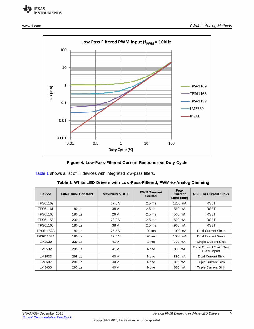
Figure 4 shows the response of four white-LED drivers that incorporate a low-pass-filtered PWM input.The TPS61169 is a low-cost device, which shows a lot of low current offset error. The LM3530 is an I2C-controlled device with its PWM input used for CABC control. The TPS61165 and the TPS61158 are simplePWM-only controlled devices that have their offset voltages much better managed. All of these deviceshave been designed to ensure a positive offset voltage. To allow the ability for 0 duty cycle to force 0current, these devices incorporate a time-out counter on their PWM input. Ths counter starts when PWMgoes low, and if a rising edge is not seen before the counter times out, the boost is forced off.
Figure 3. Offset Error in Feedback Voltage
0.001
0.01
0.1
1
10
100
0.01 0.1 1 10 100
ILE
D (
mA
)
Duty Cycle (%)
Low Pass Filtered PWM Input (fPWM = 10kHz)
TPS61169
TPS61165
TPS61158
LM3530
IDEAL
www.ti.com PWM-to-Analog Methods
5SNVA768–December 2016Submit Documentation Feedback
Copyright © 2016, Texas Instruments Incorporated
Analog PWM Dimming in White-LED Drivers
Figure 4. Low-Pass-Filtered Current Response vs Duty Cycle
Table 1 shows a list of TI devices with integrated low-pass filters.
Table 1. White LED Drivers with Low-Pass-Filtered, PWM-to-Analog Dimming
Device Filter Time Constant Maximum VOUT PWM TimeoutCounter
PeakCurrent
Limit (min)RSET or Current Sinks
TPS61169 37.5 V 2.5 ms 1200 mA RSETTPS61161 180 µs 38 V 2.5 ms 560 mA RSETTPS61160 180 µs 26 V 2.5 ms 560 mA RSETTPS61158 230 µs 28.2 V 2.5 ms 500 mA RSETTPS61165 180 µs 38 V 2.5 ms 960 mA RSET
TPS61162A 180 µs 26.5 V 20 ms 1000 mA Dual Current SinksTPS61163A 180 µs 37.5 V 20 ms 1000 mA Dual Current Sinks
LM3530 330 µs 41 V 2 ms 739 mA Single Current Sink
LM3532 295 µs 41 V None 880 mA Triple Current Sink (DualPWM Input)
LM3533 295 µs 40 V None 880 mA Dual Current SinkLM3697 295 µs 40 V None 880 mA Triple Current SinkLM3633 295 µs 40 V None 880 mA Triple Current Sink
PWM
RamperMapper
(Exponential/Linear
DAC
Current Sink 1
Current Sink 2
ILED1 ILED2
I2C
11
11
11 11
Analog Domain
Boost
Min VHR
Vout
DACi
Current Sink 3
ILED3
Programmable Ramp Rates
Copyright © 2016, Texas Instruments Incorporated
PWM-to-Analog Methods www.ti.com
6 SNVA768–December 2016Submit Documentation Feedback
Copyright © 2016, Texas Instruments Incorporated
Analog PWM Dimming in White-LED Drivers
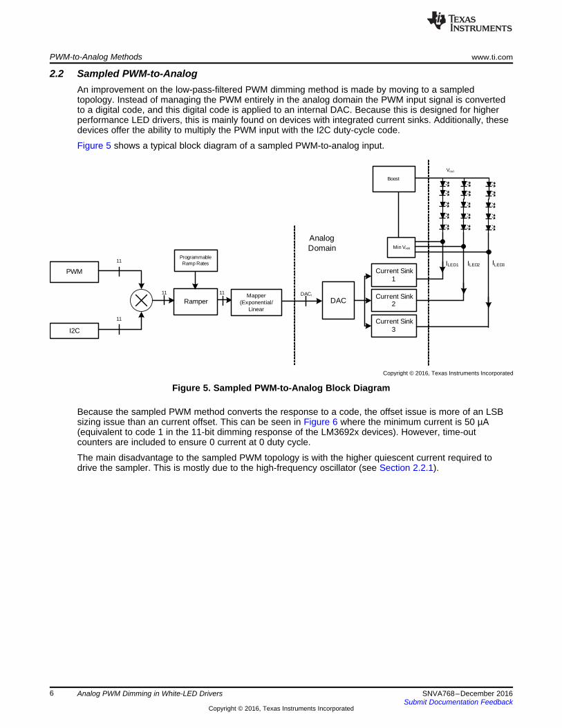
2.2 Sampled PWM-to-AnalogAn improvement on the low-pass-filtered PWM dimming method is made by moving to a sampledtopology. Instead of managing the PWM entirely in the analog domain the PWM input signal is convertedto a digital code, and this digital code is applied to an internal DAC. Because this is designed for higherperformance LED drivers, this is mainly found on devices with integrated current sinks. Additionally, thesedevices offer the ability to multiply the PWM input with the I2C duty-cycle code.
Figure 5 shows a typical block diagram of a sampled PWM-to-analog input.
Figure 5. Sampled PWM-to-Analog Block Diagram
Because the sampled PWM method converts the response to a code, the offset issue is more of an LSBsizing issue than an current offset. This can be seen in Figure 6 where the minimum current is 50 µA(equivalent to code 1 in the 11-bit dimming response of the LM3692x devices). However, time-outcounters are included to ensure 0 current at 0 duty cycle.
The main disadvantage to the sampled PWM topology is with the higher quiescent current required todrive the sampler. This is mostly due to the high-frequency oscillator (see Section 2.2.1).

0.001
0.01
0.1
1
10
100
0.01 0.1 1 10 100
ILE
D (
mA
)
Sampled PWM Input (fPWM = 10kHz)
LM36923
IDEAL
www.ti.com PWM-to-Analog Methods
7SNVA768–December 2016Submit Documentation Feedback
Copyright © 2016, Texas Instruments Incorporated
Analog PWM Dimming in White-LED Drivers
Figure 6. Sampled PWM Current Response vs Duty Cycle
The main advantages of the sampled PWM method (over the LPF) are the following:1. Allows for mapping the PWM input to an exponential dimming curve (or any other mapping mode
available).2. Allows LED current ramping between duty cycle changes. Using programmable ramping can translate
low-resolution PWM duty cycle inputs into higher resolution current ramping.3. Digital filters (programmable hysteresis) can be used to eliminate jitter in the PWM input that might
cause flicker in the LED brightness.4. Allows for very low frequency PWM inputs. Because the PWM input is converted to a digital code it
avoids large low pass filters that would be required for low frequency PWM.5. Allows a faster response to duty-cycle changes. Because the PWM sample clock is much higher than
the PWM input frequency, any change in duty cycle is interpreted within a single PWM period.However, for large deviations in the PWM duty cycle, the slew of the LED voltage can become thebottleneck.
Table 2. White LED Drivers With Sampled PWM-to-Analog Dimming
Device Sample Rate Options Configuration VOUT Range Other FeaturesLM36922 800 kHz/4 MHz/24 MHz 2 strings Up to 28 V NoneLM36923 800 kHz/4 MHz/24 MHz 3 strings Up to 28 V None
LM36922H 800 kHz/4 MHz/24 MHz 2 strings Up to 38 V NoneLM36923H 800 kHz/4 MHz/24 MHz 3 strings Up to 38 V None
LM3631 24 MHz 2 strings Up to 28 V Integrated LCD bias withprogrammable turnon
LM36272 1 MHz/4 MHz/24 MHz 2 strings Up to 28 V Integrated LCD biasLM36273 1 MHz/4 MHz/24 MHz 3 strings Up to 28 V Integrated LCD biasLM36274 1 MHz/4 MHz/24 MHz 4 strings Up to 28 V Integrated LCD bias

6
7
8
9
10
11
12
30 300 3000 30000
Ma
xim
um
Ach
iev
ab
le R
eso
luti
on
(b
its)
Input PWM Frequency
LED Current Resolution vs PWM Input Frequency and PWM Sample Rate
800kHz
4MHz
24MHz
PWM-to-Analog Methods www.ti.com
8 SNVA768–December 2016Submit Documentation Feedback
Copyright © 2016, Texas Instruments Incorporated
Analog PWM Dimming in White-LED Drivers
2.2.1 Programmable Sample RateThe PWM sampler can require high frequency oscillators, depending on the PWM input frequency andresolution required, which can result in high quiescent current. Having a programmable sample frequencycan help better fit the sample clock to the input PWM frequency and thus save on quiescent power.Table 2 lists some of the LED driver parts with a sampled PWM input to an analog LED current.
Figure 7 shows the useful PWM input frequency and resolution achievable for the 3 different sample rateoptions in the LM3692x family of white LED drivers. These curves are generated from the following (MAXResolution = LN(fSAMPLE/fPWM)/LN(2)). The devices in Table 2 all have a maximum resolution of 11 bits.Additionally, the PWM timeout counter is adjusted depending on the sample rate, so this gives a minimumachievable PWM input frequency based on sample rate options.
Figure 7. PWM Sample Rate Options (LM36923x Devices)
Table 3 shows the sample rate options/PWM timeout, and the corresponding increase in quiescent currentfor each sample rate option.
Table 3. Programmable Sample Frequencies (LM3692x Devices)
PWM Sample Rate Input QuiescentCurrent (mA) For
PWM Sampler
Frequency Rangefor 11-Bit Resolution
PWM Timeout fPWM Minimum
800 kHz 30 µA fPWM < 400 Hz 25 ms 48 Hz4 MHz 50 µA fPWM < 2 KHz 3 ms 400 Hz
24 MHz 350 µA fPWM < 12 kHz 600 µs 2 kHz

tJITTER tJITTER
1/fPWM
D/fPWM
1. The amount of hysteresis needed depends on the amount of
variation in the PWM period tJITTER
2. Because hysteresis is in terms of 11 bit LSBs, the hysteresis setting
would be given as: Hysteresis Setting > LN(tJITTER × fPWM × 2048)/LN(2)
www.ti.com PWM-to-Analog Methods
9SNVA768–December 2016Submit Documentation Feedback
Copyright © 2016, Texas Instruments Incorporated
Analog PWM Dimming in White-LED Drivers
2.2.2 PWM HysteresisAnother benefit of the sampled PWM input is the ability to program the hysteresis. Hysteresis helps filterout jitter in the PWM input that could cause LED flicker (predominately at light currents). Jitter causes atime varying PWM frequency that could result in a time varying duty cycle. If the duty cycle variation islarge and slow enough, this could appear as flicker at the LED output. Hysteresis works by controlling theamount of change in the LED current in response to a direction change in the PWM input duty cycle. Thismeans that for successive increases or successive decreases in duty cycle, the LED current changes atthe minimum step size. However, if the duty cycle had been increasing and then turned and begandecreasing, the initial change in duty cycle in the decreasing direction would have to overcome thehysteresis before the LED current is allowed to change. This effectively prevents the PWM jitter frombeing passed through to the LED current by keeping the LED current from changing in the oppositedirection from the previous change, until the hysteresis is overcome.
Figure 8. Determining PWM Hysteresis Based on Jitter
For the devices listed in Table 2 the programmable hysteresis is set in increments of LSBs. Table 4 showsthe hysteresis options in the LM36922/23/22H/23H.
Table 4. Programmable Hysteresis Options (LM3692x Devices)
Hysteresis Setting Minimum Duty cycle change required to overcomehysteresis (2HYST/2047
0 LSB (no hysteresis) 0.0489%1 LSB 0.0978%2 LSB 0.195%3 LSB 0.39%4 LSB 0.781%5 LSB 1.56%6 LSB 3.13%
For example, if 3 LSBs are selected for the hysteresis, then when the duty cycle direction changes, it mustchange greater than ( 24/2047 = 0.781%) for the LED current to also change. Once the initial change isovercome then subsequent changes (in the same direction) can then change at a single LSB (1/2047 =0.0489%).

0
5
10
15
20
25
0 10 20 30 40 50 60 70 80 90 100
ILE
D (
mA
)
Duty cycle (%)
ILED vs Duty Cycle
Exponential Mapping
Linear Mapping
PWM-to-Analog Methods www.ti.com
10 SNVA768–December 2016Submit Documentation Feedback
Copyright © 2016, Texas Instruments Incorporated
Analog PWM Dimming in White-LED Drivers
2.2.3 Re-Mapping the PWM ResponseHaving the PWM input converted to a digital code allows the ability to re-map the input duty cycle to adifferent current mapping. Typically duty cycle has a linear response from D to ILED. However, when thePWM input is converted to a digital code, the code can then be re-mapped to an exponential changingcurrent. An exponential response is beneficial because it compensates for the logarithmic response of theeye (the eye perceives an exponential change as linear). Figure 9 shows the ILED vs duty cycle for theexponential mapped current compared to typical linear mapped current. The exponential mapped currentchanges by 0.3% per 1/2047 change in PWM duty cycle. All devices in Table 2 have the ability to re-mapthe PWM input duty cycle to an exponential current.
Figure 9. LED Current-Mapping-Mode Options
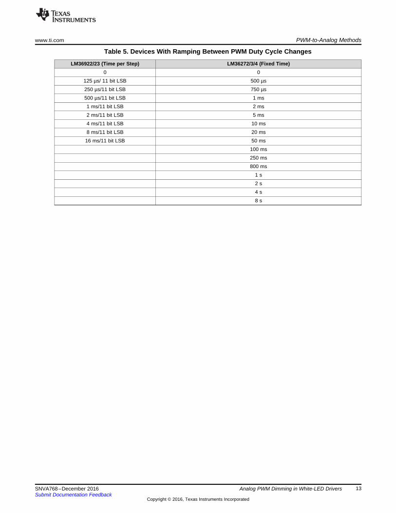
2.2.4 Automatic Current RampingOnce the PWM input is converted to a digital code, the code can be applied to any preset internal currentramps. Table 5 shows the ramp options available in some devices with sampled PWM inputs. Theseramps have two main benefits. First, automatic ramping provides a controlled turnon and turnoff withoutthe need to manage the PWM duty cycle ramp. Second, automatic ramping steps through the brightnesscodes independent of the resolution of the PWM input. This allows for low resolution input duty cycle (orstep change in input duty cycle) to give a high resolution LED current response. An example would be asystem with a low resolution duty cycle (that is, 32 levels). When the duty cycle changes, for example from50% to 100%, and ramping is enabled, the LED current increments at the programmed ramp rate, througheach available current setting, until the end duty cycle is reached (see Figure 10). This would effectivelyincrease the 32-level PWM input to a 2047-level current ramp. For some devices the ramping can be setas a time per code, and some devices have this ramp given as a fixed time between codes.
Figure 11 shows the effect of an 8-bit PWM input being gained up to an 11-bit linear and an 11-bitexponential mapping.

D = 50% D = 100%
15mA
(IINITIAL)
30mA
(IFINAL)
tRAMP
tSTEP
1. For devices with fixed time ramping, tRAMP is the programmed ramp time
independent of the number of code changes between endpoints
2. For devices with time per step ramping, tRAMP is equal to # Codes between
IFINAL and IINITIAL multiplied by the programmed time per step
www.ti.com PWM-to-Analog Methods
11SNVA768–December 2016Submit Documentation Feedback
Copyright © 2016, Texas Instruments Incorporated
Analog PWM Dimming in White-LED Drivers
Figure 10. LED Current Ramping With Duty Cycle Changes
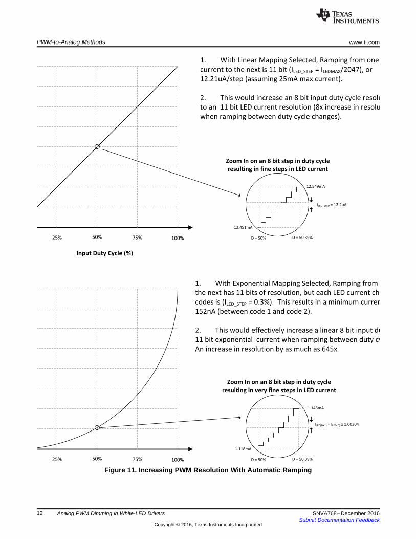
Input Duty Cycle (%)
25% 50% 75% 100% D = 50% D = 50.39%
12.451mA
12.549mA
ILED_STEP = 12.2uA
Zoom In on an 8 bit step in duty cycle
resulting in fine steps in LED current
25% 50% 75% 100%
1. With Exponential Mapping Selected, Ramping from o
the next has 11 bits of resolution, but each LED current chan
codes is (ILED_STEP = 0.3%). This results in a minimum current
152nA (between code 1 and code 2).
2. This would effectively increase a linear 8 bit input dut
11 bit exponential current when ramping between duty cyc
An increase in resolution by as much as 645x
D = 50% D = 50.39%
1.118mA
1.145mA
ILED(D+1) = ILED(D) x 1.00304
1. With Linear Mapping Selected, Ramping from one
current to the next is 11 bit (ILED_STEP = ILEDMAX/2047), or
12.21uA/step (assuming 25mA max current).
2. This would increase an 8 bit input duty cycle resolut
to an 11 bit LED current resolution (8x increase in resoluti
when ramping between duty cycle changes).
Zoom In on an 8 bit step in duty cycle
resulting in very fine steps in LED current
PWM-to-Analog Methods www.ti.com
12 SNVA768–December 2016Submit Documentation Feedback
Copyright © 2016, Texas Instruments Incorporated
Analog PWM Dimming in White-LED Drivers
Figure 11. Increasing PWM Resolution With Automatic Ramping
www.ti.com PWM-to-Analog Methods
13SNVA768–December 2016Submit Documentation Feedback
Copyright © 2016, Texas Instruments Incorporated
Analog PWM Dimming in White-LED Drivers
Table 5. Devices With Ramping Between PWM Duty Cycle Changes
LM36922/23 (Time per Step) LM36272/3/4 (Fixed Time)0 0
125 µs/ 11 bit LSB 500 µs250 µs/11 bit LSB 750 µs500 µs/11 bit LSB 1 ms1 ms/11 bit LSB 2 ms2 ms/11 bit LSB 5 ms4 ms/11 bit LSB 10 ms8 ms/11 bit LSB 20 ms
16 ms/11 bit LSB 50 ms100 ms250 ms800 ms
1 s2 s4 s8 s

IMPORTANT NOTICE
Texas Instruments Incorporated and its subsidiaries (TI) reserve the right to make corrections, enhancements, improvements and otherchanges to its semiconductor products and services per JESD46, latest issue, and to discontinue any product or service per JESD48, latestissue. Buyers should obtain the latest relevant information before placing orders and should verify that such information is current andcomplete. All semiconductor products (also referred to herein as “components”) are sold subject to TI’s terms and conditions of salesupplied at the time of order acknowledgment.TI warrants performance of its components to the specifications applicable at the time of sale, in accordance with the warranty in TI’s termsand conditions of sale of semiconductor products. Testing and other quality control techniques are used to the extent TI deems necessaryto support this warranty. Except where mandated by applicable law, testing of all parameters of each component is not necessarilyperformed.TI assumes no liability for applications assistance or the design of Buyers’ products. Buyers are responsible for their products andapplications using TI components. To minimize the risks associated with Buyers’ products and applications, Buyers should provideadequate design and operating safeguards.TI does not warrant or represent that any license, either express or implied, is granted under any patent right, copyright, mask work right, orother intellectual property right relating to any combination, machine, or process in which TI components or services are used. Informationpublished by TI regarding third-party products or services does not constitute a license to use such products or services or a warranty orendorsement thereof. Use of such information may require a license from a third party under the patents or other intellectual property of thethird party, or a license from TI under the patents or other intellectual property of TI.Reproduction of significant portions of TI information in TI data books or data sheets is permissible only if reproduction is without alterationand is accompanied by all associated warranties, conditions, limitations, and notices. TI is not responsible or liable for such altereddocumentation. Information of third parties may be subject to additional restrictions.Resale of TI components or services with statements different from or beyond the parameters stated by TI for that component or servicevoids all express and any implied warranties for the associated TI component or service and is an unfair and deceptive business practice.TI is not responsible or liable for any such statements.Buyer acknowledges and agrees that it is solely responsible for compliance with all legal, regulatory and safety-related requirementsconcerning its products, and any use of TI components in its applications, notwithstanding any applications-related information or supportthat may be provided by TI. Buyer represents and agrees that it has all the necessary expertise to create and implement safeguards whichanticipate dangerous consequences of failures, monitor failures and their consequences, lessen the likelihood of failures that might causeharm and take appropriate remedial actions. Buyer will fully indemnify TI and its representatives against any damages arising out of the useof any TI components in safety-critical applications.In some cases, TI components may be promoted specifically to facilitate safety-related applications. With such components, TI’s goal is tohelp enable customers to design and create their own end-product solutions that meet applicable functional safety standards andrequirements. Nonetheless, such components are subject to these terms.No TI components are authorized for use in FDA Class III (or similar life-critical medical equipment) unless authorized officers of the partieshave executed a special agreement specifically governing such use.Only those TI components which TI has specifically designated as military grade or “enhanced plastic” are designed and intended for use inmilitary/aerospace applications or environments. Buyer acknowledges and agrees that any military or aerospace use of TI componentswhich have not been so designated is solely at the Buyer's risk, and that Buyer is solely responsible for compliance with all legal andregulatory requirements in connection with such use.TI has specifically designated certain components as meeting ISO/TS16949 requirements, mainly for automotive use. In any case of use ofnon-designated products, TI will not be responsible for any failure to meet ISO/TS16949.
Products ApplicationsAudio www.ti.com/audio Automotive and Transportation www.ti.com/automotiveAmplifiers amplifier.ti.com Communications and Telecom www.ti.com/communicationsData Converters dataconverter.ti.com Computers and Peripherals www.ti.com/computersDLP® Products www.dlp.com Consumer Electronics www.ti.com/consumer-appsDSP dsp.ti.com Energy and Lighting www.ti.com/energyClocks and Timers www.ti.com/clocks Industrial www.ti.com/industrialInterface interface.ti.com Medical www.ti.com/medicalLogic logic.ti.com Security www.ti.com/securityPower Mgmt power.ti.com Space, Avionics and Defense www.ti.com/space-avionics-defenseMicrocontrollers microcontroller.ti.com Video and Imaging www.ti.com/videoRFID www.ti-rfid.comOMAP Applications Processors www.ti.com/omap TI E2E Community e2e.ti.comWireless Connectivity www.ti.com/wirelessconnectivity
Mailing Address: Texas Instruments, Post Office Box 655303, Dallas, Texas 75265Copyright © 2016, Texas Instruments Incorporated