Analog Interfacing Networks for DAC348x and … Interfacing Networks for DAC348x and Modulators ......
23
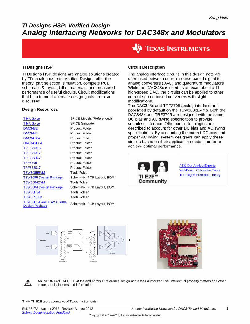
TRF3705 LO 50 DAC348x IOUTA IOUTB IOUTAP IOUTAN IOUTBP IOUTBN Source Termination Load Termination 50 50 50 VDAC VMOD Kang Hsia TI Designs HSP: Verified Design Analog Interfacing Networks for DAC348x and Modulators TI Designs HSP Circuit Description TI Designs HSP designs are analog solutions created The analog interface circuits in this design note are by TI’s analog experts. Verified Designs offer the often used between current-source based digital-to- theory, part selection, simulation, complete PCB analog converters (DAC) and quadrature modulators. schematic & layout, bill of materials, and measured While the DAC348x is used as an example of a TI performance of useful circuits. Circuit modifications high-speed DAC, the circuits can be applied to other that help to meet alternate design goals are also current-source based converters with slight discussed. modifications. The DAC348x and TRF3705 analog interface are Design Resources populated by default on the TSW308xEVMs. Both the DAC348x and TRF3705 are designed with the same TINA Spice SPICE Models (Referenced) DC bias and AC swing specification to provide TINA Spice SPICE Simulator seamless interface. Other circuit topologies are DAC3482 Product Folder described to account for other DC bias and AC swing specifications. By accounting the correct DC bias and DAC3484 Product Folder proper AC swing, system designers can apply these DAC34H84 Product Folder circuits based on their application needs in order to DAC34SH84 Product Folder achieve optimal performance. TRF370315 Product Folder TRF370317 Product Folder TRF370417 Product Folder TRF3705 Product Folder ASK Our Analog Experts TRF372017 Product Folder WebBench Calculator Tools TSW3085EVM Tools Folder TI Designs Precision Library TSW3085 Design Package Schematic, PCB Layout, BOM TSW3084EVM Tools Folder TSW3084 Design Package Schematic, PCB Layout, BOM TSW30H84 Tools Folder TSW30SH84 Tools Folder TSW30H84 and TSW30SH84 Schematic, PCB Layout, BOM Design Package An IMPORTANT NOTICE at the end of this TI reference design addresses authorized use, intellectual property matters and other important disclaimers and information. TINA-TI, E2E are trademarks of Texas Instruments. 1 SLUA647A – August 2012 – Revised August 2013 Analog Interfacing Networks for DAC348x and Modulators Submit Documentation Feedback Copyright © 2012–2013, Texas Instruments Incorporated
Transcript of Analog Interfacing Networks for DAC348x and … Interfacing Networks for DAC348x and Modulators ......
TRF3705
�
LO
50 �
DAC348x
IOUTA
IOUTB
IOUTAPIOUTAN
IOUTBPIOUTBN
SourceTermination
LoadTermination
50 �
50 �
50 �
VDAC VMOD
Kang Hsia
TI Designs HSP: Verified DesignAnalog Interfacing Networks for DAC348x and Modulators
TI Designs HSP Circuit DescriptionTI Designs HSP designs are analog solutions created The analog interface circuits in this design note areby TI’s analog experts. Verified Designs offer the often used between current-source based digital-to-theory, part selection, simulation, complete PCB analog converters (DAC) and quadrature modulators.schematic & layout, bill of materials, and measured While the DAC348x is used as an example of a TIperformance of useful circuits. Circuit modifications high-speed DAC, the circuits can be applied to otherthat help to meet alternate design goals are also current-source based converters with slightdiscussed. modifications.
The DAC348x and TRF3705 analog interface areDesign Resources populated by default on the TSW308xEVMs. Both the
DAC348x and TRF3705 are designed with the sameTINA Spice SPICE Models (Referenced) DC bias and AC swing specification to provideTINA Spice SPICE Simulator seamless interface. Other circuit topologies areDAC3482 Product Folder described to account for other DC bias and AC swing
specifications. By accounting the correct DC bias andDAC3484 Product Folderproper AC swing, system designers can apply theseDAC34H84 Product Foldercircuits based on their application needs in order toDAC34SH84 Product Folderachieve optimal performance.TRF370315 Product Folder
TRF370317 Product FolderTRF370417 Product FolderTRF3705 Product Folder
ASK Our Analog ExpertsTRF372017 Product FolderWebBench Calculator Tools
TSW3085EVM Tools FolderTI Designs Precision Library
TSW3085 Design Package Schematic, PCB Layout, BOMTSW3084EVM Tools FolderTSW3084 Design Package Schematic, PCB Layout, BOMTSW30H84 Tools FolderTSW30SH84 Tools FolderTSW30H84 and TSW30SH84 Schematic, PCB Layout, BOMDesign Package
An IMPORTANT NOTICE at the end of this TI reference design addresses authorized use, intellectual property matters and otherimportant disclaimers and information.
TINA-TI, E2E are trademarks of Texas Instruments.
1SLUA647A–August 2012–Revised August 2013 Analog Interfacing Networks for DAC348x and ModulatorsSubmit Documentation Feedback
Copyright © 2012–2013, Texas Instruments Incorporated
Introduction www.ti.com
1 IntroductionThe DAC348x family provides high-performance digital-to-analog conversion (DAC) for many applications.The DAC is often part of the signal chain in the system with many down-stream analog components suchas amplifiers, I/Q modulators, or mixers attached. While some are custom fit by design, typically, thesedown-stream analog components have different biasing, AC swing, and impedance requirements that aredifferent than the DAC348x family. Therefore, achieving optimal performance requires proper design of theinterfacing network. This reference design covers various interface-network options and designconsiderations for the TI modulators. These examples serve as guidelines in the design of interfacenetworks for various down-stream analog components.
2 Definitions
IOUTFS: the full-scale output current of the DAC348x. Nominally set to 20 mA in thisdocument.
VDAC: any DAC output nodes: IOUTAp, IOUTAn, etc.VMOD: any modulator input nodes: BBIp, BBIn, etc.
IDAC_DC: the average DAC output current. For 20-mA FS, IDAC_DC = 10 mA.REQ_MOD: the equivalent DC resistance of the modulator input.
VCC: positive bias supply for the dual-supplies bias interface-network.VEE: negative bias supply for the dual-supplies bias interface-network.
VBIAS bias supply for the single-supply bias interface-network
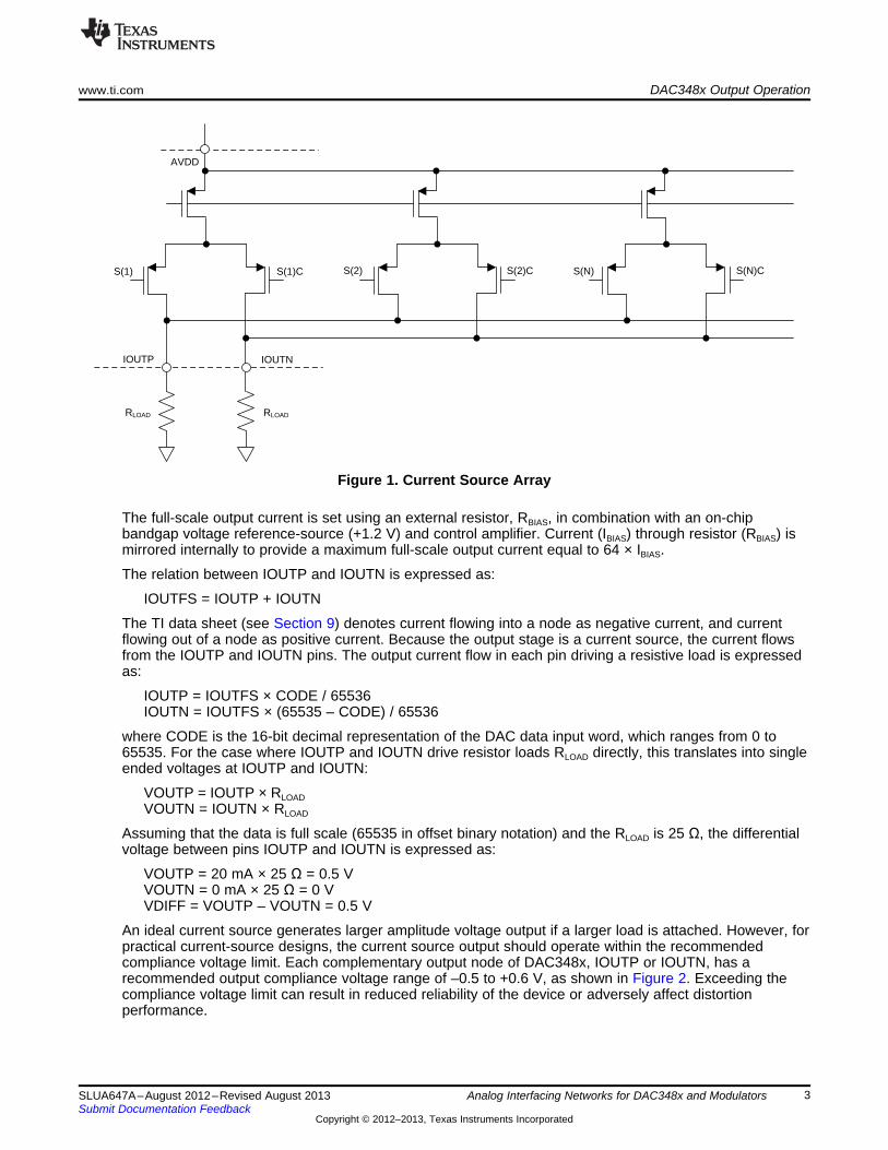
3 DAC348x Output OperationThe DAC348x is a CMOS current output digital-to-analog converter (DAC). Therefore, the amplitude of theoutput voltage depends on the output load impedance with a V = IR relationship. The DAC consists of asegmented array of PMOS current sources which are capable of sourcing a full-scale output current up to30 mA.
The equivalent circuit of this output is represented as a current source controlled by the DAC input digitalcode, as shown in Figure 1. Each bit causes the current source to switch out a fixed amount of current.The output architecture requires that both the complementary output nodes, IOUTP and IOUTN, terminateto ground. Differential current switches direct the current to either one of the complementary output nodes.Complementary output currents enable differential operations, thus canceling output common-mode noisesources (digital feed-through, and both on-chip and PCB noise), DC offsets, even-order distortioncomponents, and increasing signal-output power by a factor of four.
2 Analog Interfacing Networks for DAC348x and Modulators SLUA647A–August 2012–Revised August 2013Submit Documentation Feedback
Copyright © 2012–2013, Texas Instruments Incorporated
AVDD
S(1) S(1)C S(2) S(2)C S(N) S(N)C
IOUTP IOUTN
RLOAD RLOAD
www.ti.com DAC348x Output Operation
Figure 1. Current Source Array
The full-scale output current is set using an external resistor, RBIAS, in combination with an on-chipbandgap voltage reference-source (+1.2 V) and control amplifier. Current (IBIAS) through resistor (RBIAS) ismirrored internally to provide a maximum full-scale output current equal to 64 × IBIAS.
The relation between IOUTP and IOUTN is expressed as:
IOUTFS = IOUTP + IOUTN
The TI data sheet (see Section 9) denotes current flowing into a node as negative current, and currentflowing out of a node as positive current. Because the output stage is a current source, the current flowsfrom the IOUTP and IOUTN pins. The output current flow in each pin driving a resistive load is expressedas:
IOUTP = IOUTFS × CODE / 65536IOUTN = IOUTFS × (65535 – CODE) / 65536
where CODE is the 16-bit decimal representation of the DAC data input word, which ranges from 0 to65535. For the case where IOUTP and IOUTN drive resistor loads RLOAD directly, this translates into singleended voltages at IOUTP and IOUTN:
VOUTP = IOUTP × RLOADVOUTN = IOUTN × RLOAD
Assuming that the data is full scale (65535 in offset binary notation) and the RLOAD is 25 Ω, the differentialvoltage between pins IOUTP and IOUTN is expressed as:
VOUTP = 20 mA × 25 Ω = 0.5 VVOUTN = 0 mA × 25 Ω = 0 VVDIFF = VOUTP – VOUTN = 0.5 V
An ideal current source generates larger amplitude voltage output if a larger load is attached. However, forpractical current-source designs, the current source output should operate within the recommendedcompliance voltage limit. Each complementary output node of DAC348x, IOUTP or IOUTN, has arecommended output compliance voltage range of –0.5 to +0.6 V, as shown in Figure 2. Exceeding thecompliance voltage limit can result in reduced reliability of the device or adversely affect distortionperformance.
3SLUA647A–August 2012–Revised August 2013 Analog Interfacing Networks for DAC348x and ModulatorsSubmit Documentation Feedback
Copyright © 2012–2013, Texas Instruments Incorporated
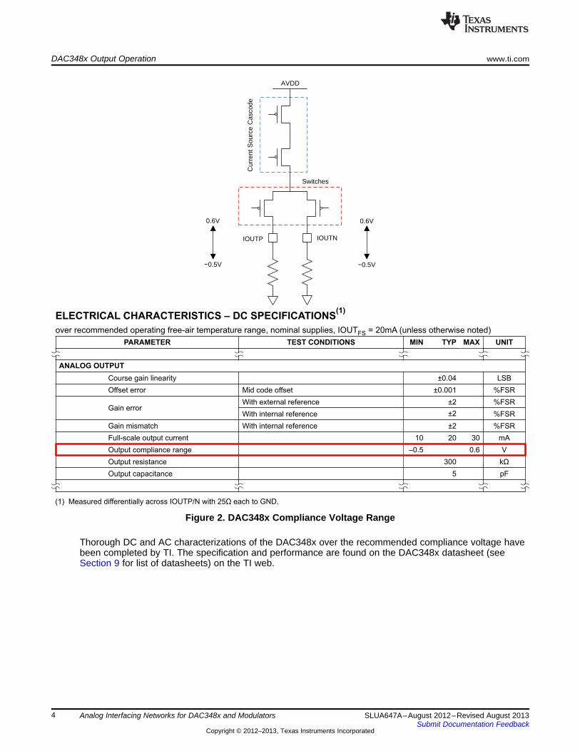
PARAMETER TEST CONDITIONS MIN TYP MAX UNIT
ANALOG OUTPUT
Course gain linearity ±0.04 LSB
Offset error Mid code offset ±0.001 %FSR
Gain errorWith external reference ±2 %FSR
With internal reference ±2 %FSR
Gain mismatch With internal reference ±2 %FSR
Full-scale output current 10 20 30 mA
Output compliance range –0.5 0.6 V
Output resistance 300 kΩ
Output capacitance 5 pF
over recommended operating free-air temperature range, nominal supplies, IOUT = 20mA (unless otherwise noted)FS
(1) Measured differentially across IOUTP/N with 25 each to GND.Ω
ELECTRICAL CHARACTERISTICS – DC SPECIFICATIONS(1)
IOUTP IOUTN
AVDD
Switches
Cur
rent
Sou
rce
Cas
code
0.6V
í0.5V
0.6V
í0.5V
DAC348x Output Operation www.ti.com
Figure 2. DAC348x Compliance Voltage Range
Thorough DC and AC characterizations of the DAC348x over the recommended compliance voltage havebeen completed by TI. The specification and performance are found on the DAC348x datasheet (seeSection 9 for list of datasheets) on the TI web.
4 Analog Interfacing Networks for DAC348x and Modulators SLUA647A–August 2012–Revised August 2013Submit Documentation Feedback
Copyright © 2012–2013, Texas Instruments Incorporated
DC10mA
AC10mA
AVDD
DC10mA
AC10mA
(inverted)
AVDD
Ioutp
Ioutn
3p3A3p3A
3p3A
-
+
VCCS1 1
-
+
VCCS2 1
IS1 10mA
IS2 10mA
-
+
-
+
VCVS1 10m
+
VG1
V1 3.3V
Ioutp
Ioutn
SPICE Modeling of DAC Current Source Array Equivalent TINA-TI SPICE Model
20mA
0mA
10mAIoutp
20mA
0mA
10mAIoutn
20mA
0mA
10mAIoutpDC
20mA
0mA
10mAIoutnDC
10mA
-10mA
0mAIoutpAC
IoutnAC
10mA
-10mA
0mA
= +
www.ti.com DAC348x Output Operation
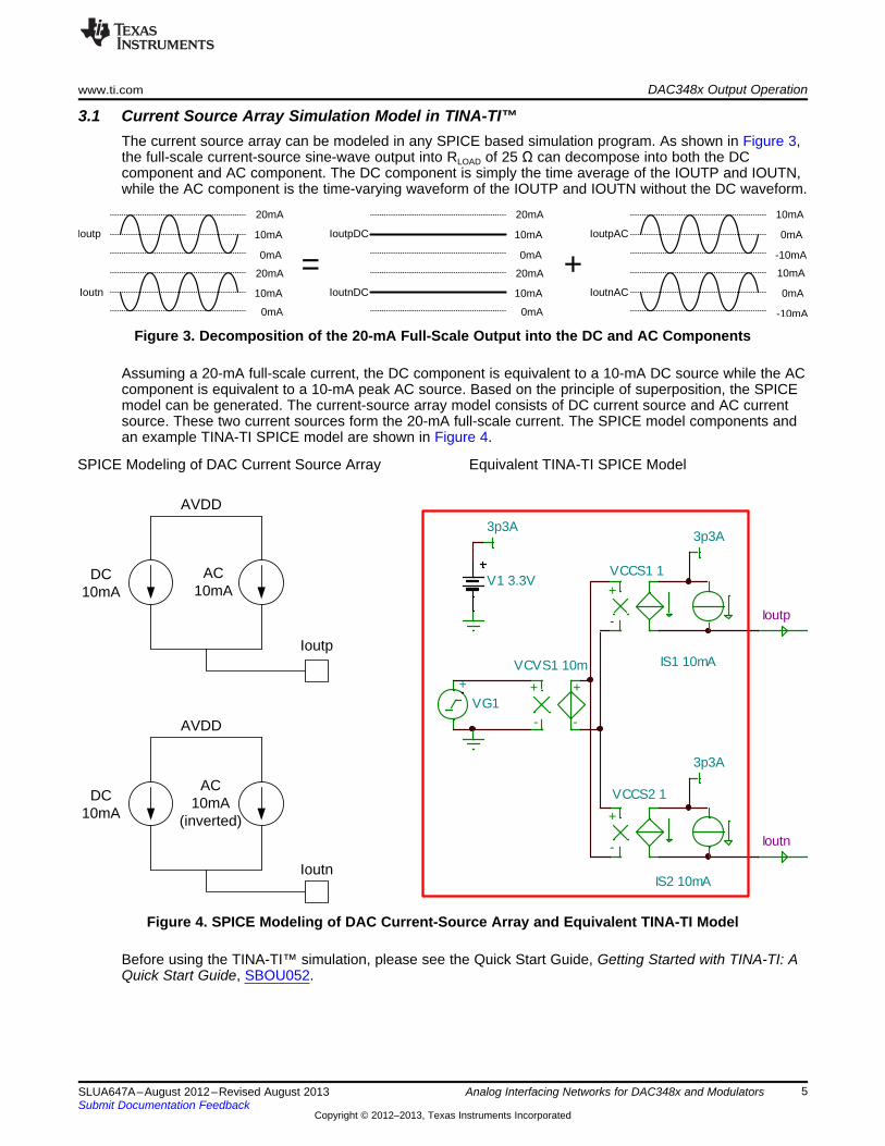
3.1 Current Source Array Simulation Model in TINA-TI™The current source array can be modeled in any SPICE based simulation program. As shown in Figure 3,the full-scale current-source sine-wave output into RLOAD of 25 Ω can decompose into both the DCcomponent and AC component. The DC component is simply the time average of the IOUTP and IOUTN,while the AC component is the time-varying waveform of the IOUTP and IOUTN without the DC waveform.
Figure 3. Decomposition of the 20-mA Full-Scale Output into the DC and AC Components
Assuming a 20-mA full-scale current, the DC component is equivalent to a 10-mA DC source while the ACcomponent is equivalent to a 10-mA peak AC source. Based on the principle of superposition, the SPICEmodel can be generated. The current-source array model consists of DC current source and AC currentsource. These two current sources form the 20-mA full-scale current. The SPICE model components andan example TINA-TI SPICE model are shown in Figure 4.
Figure 4. SPICE Modeling of DAC Current-Source Array and Equivalent TINA-TI Model
Before using the TINA-TI™ simulation, please see the Quick Start Guide, Getting Started with TINA-TI: AQuick Start Guide, SBOU052.
5SLUA647A–August 2012–Revised August 2013 Analog Interfacing Networks for DAC348x and ModulatorsSubmit Documentation Feedback
Copyright © 2012–2013, Texas Instruments Incorporated
20mA (0.5V)
IOUTAP
IOUTAN
10mA (0.25V)
0mA (0V)
20mA (0.5V)
10mA (0.25V)
0mA (0V)
0.5V
0V
í0.5V
IOUTA(Differential)
TRF3705
�
LO
50 �
DAC348x
IOUTA
IOUTB
IOUTAPIOUTAN
IOUTBPIOUTBN
SourceTermination
LoadTermination
50 �
50 �
50 �
VDAC VMOD
DAC348x to TRF3705 Interface www.ti.com
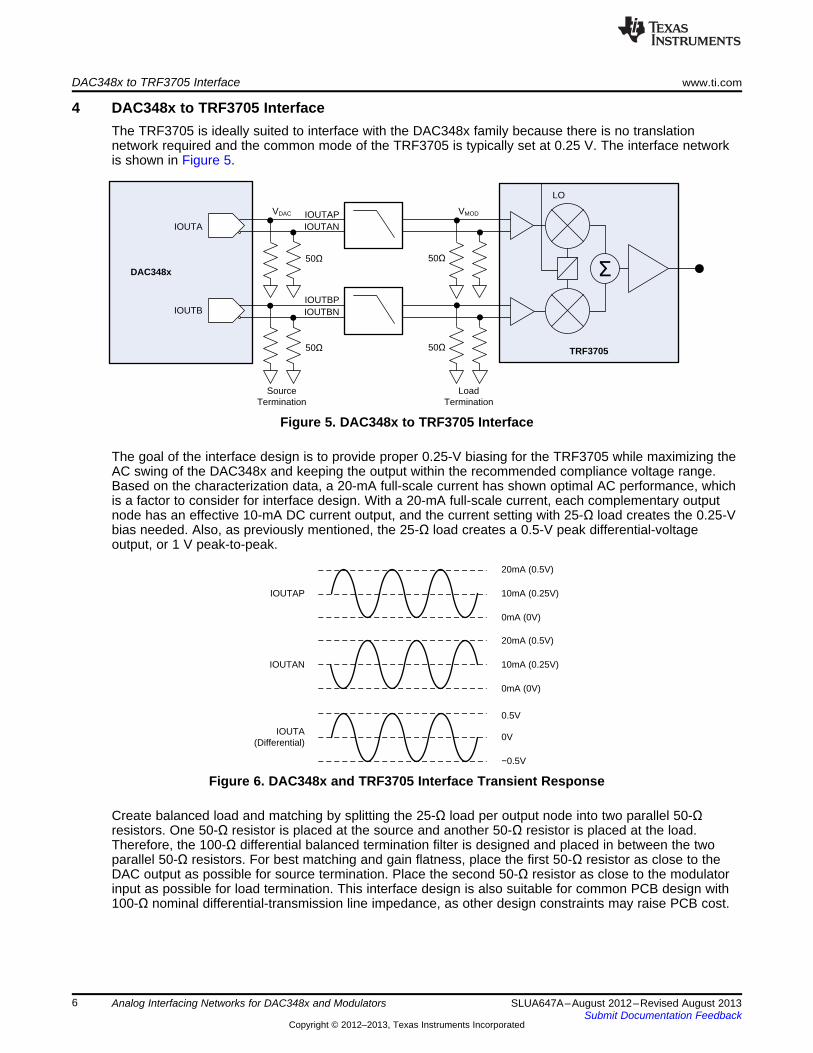
4 DAC348x to TRF3705 InterfaceThe TRF3705 is ideally suited to interface with the DAC348x family because there is no translationnetwork required and the common mode of the TRF3705 is typically set at 0.25 V. The interface networkis shown in Figure 5.
Figure 5. DAC348x to TRF3705 Interface
The goal of the interface design is to provide proper 0.25-V biasing for the TRF3705 while maximizing theAC swing of the DAC348x and keeping the output within the recommended compliance voltage range.Based on the characterization data, a 20-mA full-scale current has shown optimal AC performance, whichis a factor to consider for interface design. With a 20-mA full-scale current, each complementary outputnode has an effective 10-mA DC current output, and the current setting with 25-Ω load creates the 0.25-Vbias needed. Also, as previously mentioned, the 25-Ω load creates a 0.5-V peak differential-voltageoutput, or 1 V peak-to-peak.
Figure 6. DAC348x and TRF3705 Interface Transient Response
Create balanced load and matching by splitting the 25-Ω load per output node into two parallel 50-Ωresistors. One 50-Ω resistor is placed at the source and another 50-Ω resistor is placed at the load.Therefore, the 100-Ω differential balanced termination filter is designed and placed in between the twoparallel 50-Ω resistors. For best matching and gain flatness, place the first 50-Ω resistor as close to theDAC output as possible for source termination. Place the second 50-Ω resistor as close to the modulatorinput as possible for load termination. This interface design is also suitable for common PCB design with100-Ω nominal differential-transmission line impedance, as other design constraints may raise PCB cost.
6 Analog Interfacing Networks for DAC348x and Modulators SLUA647A–August 2012–Revised August 2013Submit Documentation Feedback
Copyright © 2012–2013, Texas Instruments Incorporated
VBIAS
AQM
�
LO
R1 DAC348x
IOUTA
IOUTB
IOUTAPIOUTAN
IOUTBPIOUTBN
SourceTermination
LoadTermination
R1
R2
R2
VDAC
VMOD
BBIPBBIN
BBQPBBQN
R4
VBIAS
R4
R3//C1
R3//C1
A3p3 A3p3
A3p3
V1 3.3V
DAC Output -
DAC Output +
-
+
VCCS1 1
-
+
VCCS2 1
IS1 10mA
IS2 10mA
-
+
-
+
VCVS1 10m
+
VG1R
1 50
Ohm
R2
50O
hm
L1 33nH
L2 33nHC
4 3.
3pF
C5
3.3p
F
Mod Input +
Mod Input -
V+
VM1
R11
50O
hm
C1
4.6p
FC
6 4.
6pF
R6
50O
hm
L3 0H
L4 0H
C7
1fF
C8
1fF
L5 0H
L6 0HC
9 1f
F
C10
1fF
C11
1fF
C12
1fF
C13
1fF
C14
1fF
C15
1fF
C16
1fF
R9
8kO
hmR
13 8
kOhm
TRF3705Modulator Input Model
Reconstruction Filter100ohm Matched Impedance
DAC348x20mA Full-Scale Current
www.ti.com Single-Supply Level Translation
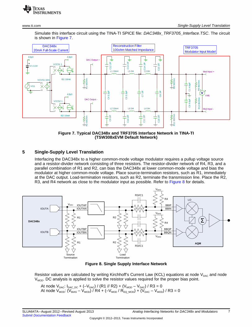
Simulate this interface circuit using the TINA-TI SPICE file: DAC348x_TRF3705_Interface.TSC. The circuitis shown in Figure 7.
Figure 7. Typical DAC348x and TRF3705 Interface Network in TINA-TI(TSW308xEVM Default Network)
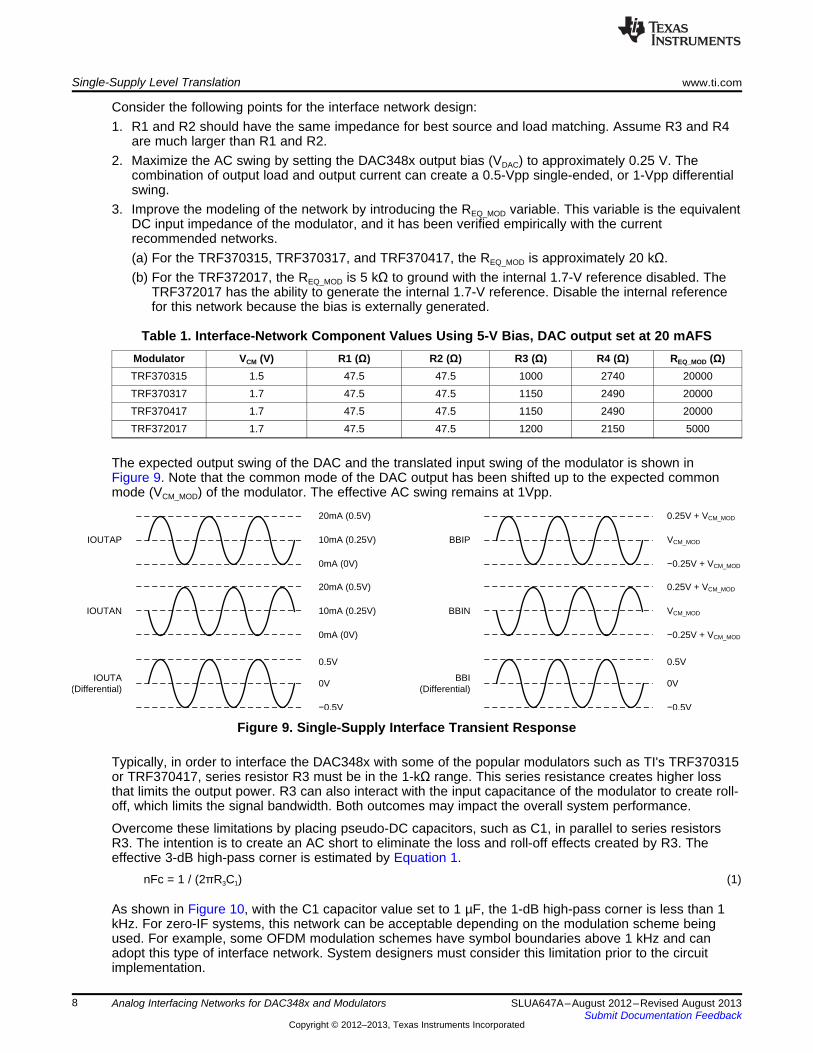
5 Single-Supply Level TranslationInterfacing the DAC348x to a higher common-mode voltage modulator requires a pullup voltage sourceand a resistor-divider network consisting of three resistors. The resistor-divider network of R4, R3, and aparallel combination of R1 and R2, can bias the DAC348x at lower common-mode voltage and bias themodulator at higher common-mode voltage. Place source-termination resistors, such as R1, immediatelyat the DAC output. Load-termination resistors, such as R2, terminate the transmission line. Place the R2,R3, and R4 network as close to the modulator input as possible. Refer to Figure 8 for details.
Figure 8. Single Supply Interface Network
Resistor values are calculated by writing Kirchhoff’s Current Law (KCL) equations at node VDAC and nodeVMOD. DC analysis is applied to solve the resistor values required for the proper bias point.
At node VDAC: IDAC_DC + (–VDAC) / (R1 // R2) + (VMOD – VDAC) / R3 = 0At node VMOD: (VBIAS – VMOD) / R4 + (–VMOD / REQ_MOD) + (VDAC – VMOD) / R3 = 0
7SLUA647A–August 2012–Revised August 2013 Analog Interfacing Networks for DAC348x and ModulatorsSubmit Documentation Feedback
Copyright © 2012–2013, Texas Instruments Incorporated
20mA (0.5V)
IOUTAP
IOUTAN
10mA (0.25V)
0mA (0V)
20mA (0.5V)
10mA (0.25V)
0mA (0V)
0.5V
0V
í0.5V
IOUTA(Differential)
0.25V + VCM_MOD
BBIP
BBIN
VCM_MOD
í0.25V + VCM_MOD
0.25V + VCM_MOD
VCM_MOD
í0.25V + VCM_MOD
0.5V
0V
í0.5V
BBI(Differential)
Single-Supply Level Translation www.ti.com
Consider the following points for the interface network design:1. R1 and R2 should have the same impedance for best source and load matching. Assume R3 and R4
are much larger than R1 and R2.2. Maximize the AC swing by setting the DAC348x output bias (VDAC) to approximately 0.25 V. The
combination of output load and output current can create a 0.5-Vpp single-ended, or 1-Vpp differentialswing.
3. Improve the modeling of the network by introducing the REQ_MOD variable. This variable is the equivalentDC input impedance of the modulator, and it has been verified empirically with the currentrecommended networks.(a) For the TRF370315, TRF370317, and TRF370417, the REQ_MOD is approximately 20 kΩ.(b) For the TRF372017, the REQ_MOD is 5 kΩ to ground with the internal 1.7-V reference disabled. The
TRF372017 has the ability to generate the internal 1.7-V reference. Disable the internal referencefor this network because the bias is externally generated.
Table 1. Interface-Network Component Values Using 5-V Bias, DAC output set at 20 mAFSModulator VCM (V) R1 (Ω) R2 (Ω) R3 (Ω) R4 (Ω) REQ_MOD (Ω)TRF370315 1.5 47.5 47.5 1000 2740 20000TRF370317 1.7 47.5 47.5 1150 2490 20000TRF370417 1.7 47.5 47.5 1150 2490 20000TRF372017 1.7 47.5 47.5 1200 2150 5000
The expected output swing of the DAC and the translated input swing of the modulator is shown inFigure 9. Note that the common mode of the DAC output has been shifted up to the expected commonmode (VCM_MOD) of the modulator. The effective AC swing remains at 1Vpp.
Figure 9. Single-Supply Interface Transient Response
Typically, in order to interface the DAC348x with some of the popular modulators such as TI's TRF370315or TRF370417, series resistor R3 must be in the 1-kΩ range. This series resistance creates higher lossthat limits the output power. R3 can also interact with the input capacitance of the modulator to create roll-off, which limits the signal bandwidth. Both outcomes may impact the overall system performance.
Overcome these limitations by placing pseudo-DC capacitors, such as C1, in parallel to series resistorsR3. The intention is to create an AC short to eliminate the loss and roll-off effects created by R3. Theeffective 3-dB high-pass corner is estimated by Equation 1.
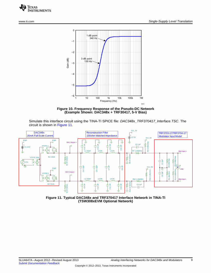
nFc = 1 / (2πR3C1) (1)
As shown in Figure 10, with the C1 capacitor value set to 1 µF, the 1-dB high-pass corner is less than 1kHz. For zero-IF systems, this network can be acceptable depending on the modulation scheme beingused. For example, some OFDM modulation schemes have symbol boundaries above 1 kHz and canadopt this type of interface network. System designers must consider this limitation prior to the circuitimplementation.
8 Analog Interfacing Networks for DAC348x and Modulators SLUA647A–August 2012–Revised August 2013Submit Documentation Feedback
Copyright © 2012–2013, Texas Instruments Incorporated
Vcc_5V
A3p3 A3p3
A3p3
Vcc_5V
Vcc_5V
V2 5V
V1 3.3V
DAC Output -
DAC Output +
-
+
VCCS1 1
-
+
VCCS2 1
IS1 10mA
IS2 10mA
-
+
-
+
VCVS1 10m
+
VG1
R1
47.5
Ohm
R2
47.5
Ohm
L1 33nH
L2 33nH
C4
3.3p
F
C5
3.3p
F
R3
2.49
kOhm
R7 1.15kOhm Mod Input +R
10 2
.49k
Ohm
R12 1.15kOhm Mod Input -
V+
VM1
R11
47.
5Ohm
R4
20kO
hm
C1
3pF
C2 1uF
C3 1uF
C6
3pF
R5
20kO
hm
R6
47.5
Ohm
L3 0H
L4 0H
C7
1fF
C8
1fF
L5 0H
L6 0H
C9
1fF
C10
1fF
C11
1fF
C12
1fF
C13
1fF
C14
1fF
C15
1fF
C16
1fF
R9
6.66
kOhm
R13
6.6
6kO
hm
TRF3703-17/TRF3704-17Modulator Input Model
Reconstruction Filter100ohm Matched Impedance
DAC348x20mA Full-Scale Current
−6
−5
−4
−3
−2
−1
0
1 10 100 1k 10k 100k 1M
Frequency (Hz)
Gain
(dB
)
G001
1 dB point340 Hz
3 dB point130 Hz
www.ti.com Single-Supply Level Translation
Figure 10. Frequency Response of the Pseudo-DC Network(Example Shown: DAC348x + TRF30417, 5-V Bias)
Simulate this interface circuit using the TINA-TI SPICE file: DAC348x_TRF370417_Interface.TSC. Thecircuit is shown in Figure 11.
Figure 11. Typical DAC348x and TRF370417 Interface Network in TINA-TI(TSW308xEVM Optional Network)
9SLUA647A–August 2012–Revised August 2013 Analog Interfacing Networks for DAC348x and ModulatorsSubmit Documentation Feedback
Copyright © 2012–2013, Texas Instruments Incorporated
2R)2
4R//3R(
2
4R//3R
nattenuatio
+
=
VCC
AQM
�
LO
DAC348x
IOUTA
IOUTB
SourceTermination
LoadTermination
R1
R1
VDAC
VMODR3
VCC
R3
R2
R2
R4
R4
VEE
VEE
Dual-Supplies Level Translation www.ti.com
6 Dual-Supplies Level TranslationSingle-supply biasing limits the DAC348x output to positive swing only. If the DAC348x output is biasedwith the available negative supply rail, the negative-compliance voltage limit is achieved. Using thismethod, the DAC348x works in applications requiring higher output swing. Two types of dual-suppliesnetworks are used: matched impedance and pseudo-DC matched impedance.
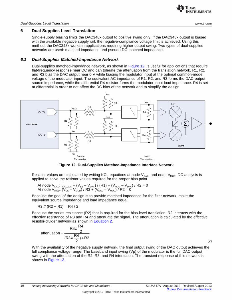
6.1 Dual-Supplies Matched-Impedance NetworkDual-supplies matched-impedance network, as shown in Figure 12, is useful for applications that requireflat-frequency response near DC and can tolerate the attenuation from the translation network. R1, R2,and R3 bias the DAC output near 0 V while biasing the modulator input at the optimal common-modevoltage of the modulator input. The equivalent AC impedance of R1, R2, and R3 forms the DAC-outputsource impedance, while the differential R4 resistor forms the modulator input load impedance. R4 is setat differential in order to not affect the DC bias of the network and to simplify the design.
Figure 12. Dual-Supplies Matched-Impedance Interface Network
Resistor values are calculated by writing KCL equations at node VDAC, and node VMOD. DC analysis isapplied to solve the resistor values required for the proper bias point.
At node VDAC: IDAC_DC + (VEE – VDAC) / (R1) + (VMOD – VDAC) / R2 = 0At node VMOD: (VCC – VMOD) / R3 + (VDAC – VMOD) / R2 = 0
Because the goal of the design is to provide matched impedance for the filter network, make theequivalent source impedance and load impedance equal.
R3 // (R2 + R1) = R4 / 2
Because the series resistance (R2) that is required for the bias-level translation, R2 interacts with theeffective resistance of R3 and R4 and attenuate the signal. The attenuation is calculated by the effectiveresistor-divider network as shown in Equation 2.
(2)
With the availability of the negative supply network, the final output swing of the DAC output achieves thefull compliance voltage range. The baseband input swing (Vp) of the modulator is the full DAC-outputswing with the attenuation of the R2, R3, and R4 interaction. The transient response of this network isshown in Figure 13.
10 Analog Interfacing Networks for DAC348x and Modulators SLUA647A–August 2012–Revised August 2013Submit Documentation Feedback
Copyright © 2012–2013, Texas Instruments Incorporated

A3p3 A3p3
A3p3
Vcc
Vcc
Vee
Vee
-
+
VCCS1 1
-
+
VCCS2 1
IS1 10mA
IS2 10mA
-
+
-
+
VCVS1 10m
+
VG1
Ioutp
Ioutn
V1 3.3V
R3
108O
hm
R7 46Ohm
R10
108
Ohm
R12 46Ohm
R11
118
Ohm
R6
118O
hm
DAC Outpu+
DAC Output-
AM
1 A
M2
AM
3 A
M4
Mod Input +
Mod Input -
V+
VM1
R4
20kO
hm
C1
3pF
C6
3pF
R5
20kO
hm
R9
6.66
kOhm
R13
6.6
6kO
hm
VMP
VMN
R1 0Ohm
R2
128O
hm
R14 0Ohm
L1 0H
L2 0H
C4
1fF
C5
1fF
L3 0H
L4 0H
C7
1fF
C8
1fF
L5 0H
L6 0H
C9
1fF
C10
1fF
C11
1fF
C12
1fF
C13
1fF
C14
1fF
C15
1fF
C16
1fF
TRF3703-15Modulator Input Model
Filter Network128ohm matched impedance (not implemented)
128ohm Filter Load(3dB Pad)
0V to 1.5V Translation Network
DAC348x20mA Full-Scale Current
20mA (0.5V)
IOUTAP
IOUTAN
10mA (0.25V)
0mA (í0.5V)
20mA (0.5V)
10mA (0.25V)
0mA (í0.5V)
1V
0V
í1V
IOUTA(Differential)
Vp + VCM_MOD
BBIP
BBIN
VCM_MOD
íVp + VCM_MOD
Vp + VCM_MOD
VCM_MOD
íVp + VCM_MOD
2Vp
0V
í2Vp
BBI(Differential)
www.ti.com Dual-Supplies Level Translation
Figure 13. Dual Supplies Matched Impedance Interface Network Transient Response
Simulate this interface circuit using the TINA-TI SPICE file:DAC348x_TRF370315_Dual_Supplies_DC.TSC. The circuit is shown in Figure 14.
Figure 14. Typical DAC348x and TRF370315 Interface with Dual-Supplies DC Network in TINA-TI.
11SLUA647A–August 2012–Revised August 2013 Analog Interfacing Networks for DAC348x and ModulatorsSubmit Documentation Feedback
Copyright © 2012–2013, Texas Instruments Incorporated
20mA (0.5V)
IOUTAP
IOUTAN
10mA (0.25V)
0mA (í0.5V)
20mA (0.5V)
10mA (0.25V)
0mA (í0.5V)
1V
0V
í1V
IOUTA(Differential)
0.5V + VCM_MOD
BBIP
BBIN
VCM_MOD
í0.5V + VCM_MOD
0.5V + VCM_MOD
VCM_MOD
í0.5V + VCM_MOD
1V
0V
í1V
BBI(Differential)
VCC
AQM
�
LO
DAC348x
IOUTA
IOUTB
SourceTermination
LoadTermination
R1
R1
VDAC
VMODR3
VCC
R3
R2//C1
R2//C1
R4
R4
VEE
VEE
Dual-Supplies Level Translation www.ti.com
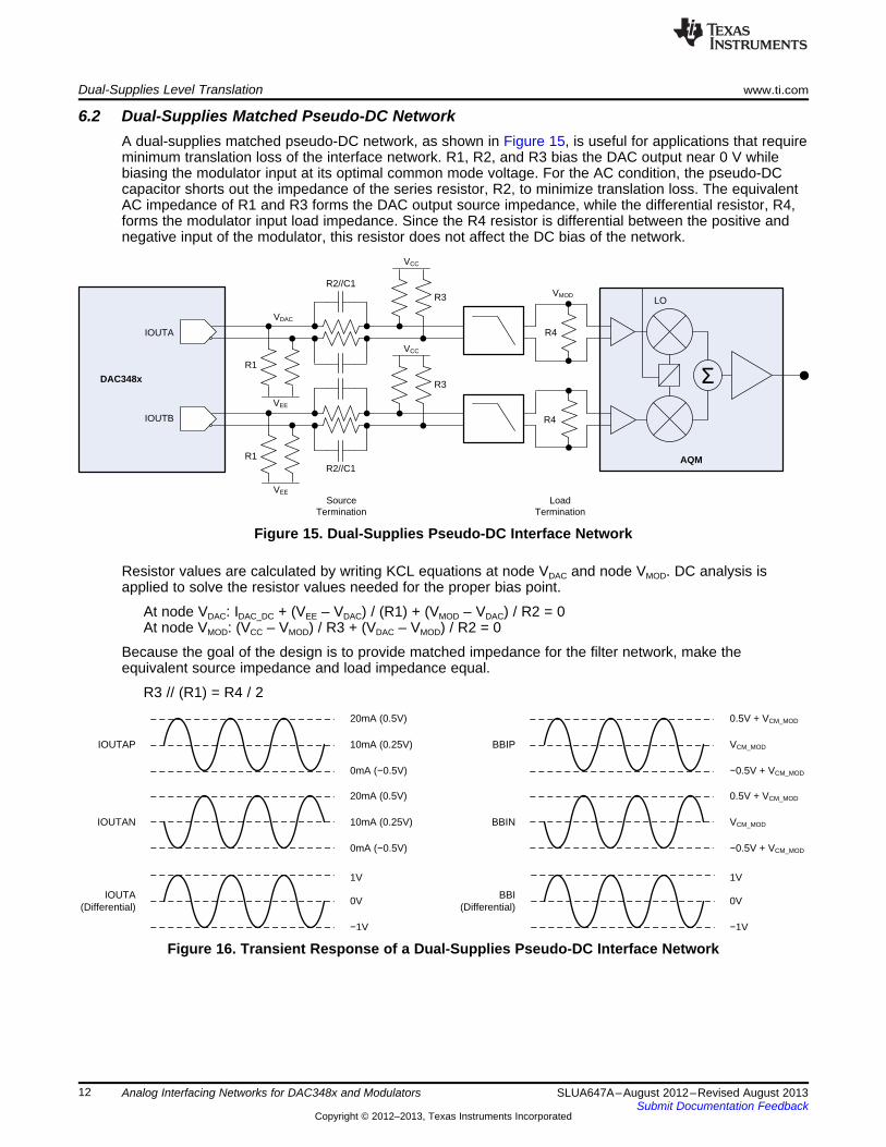
6.2 Dual-Supplies Matched Pseudo-DC NetworkA dual-supplies matched pseudo-DC network, as shown in Figure 15, is useful for applications that requireminimum translation loss of the interface network. R1, R2, and R3 bias the DAC output near 0 V whilebiasing the modulator input at its optimal common mode voltage. For the AC condition, the pseudo-DCcapacitor shorts out the impedance of the series resistor, R2, to minimize translation loss. The equivalentAC impedance of R1 and R3 forms the DAC output source impedance, while the differential resistor, R4,forms the modulator input load impedance. Since the R4 resistor is differential between the positive andnegative input of the modulator, this resistor does not affect the DC bias of the network.
Figure 15. Dual-Supplies Pseudo-DC Interface Network
Resistor values are calculated by writing KCL equations at node VDAC and node VMOD. DC analysis isapplied to solve the resistor values needed for the proper bias point.
At node VDAC: IDAC_DC + (VEE – VDAC) / (R1) + (VMOD – VDAC) / R2 = 0At node VMOD: (VCC – VMOD) / R3 + (VDAC – VMOD) / R2 = 0
Because the goal of the design is to provide matched impedance for the filter network, make theequivalent source impedance and load impedance equal.
R3 // (R1) = R4 / 2
Figure 16. Transient Response of a Dual-Supplies Pseudo-DC Interface Network
12 Analog Interfacing Networks for DAC348x and Modulators SLUA647A–August 2012–Revised August 2013Submit Documentation Feedback
Copyright © 2012–2013, Texas Instruments Incorporated
A3p3 A3p3
A3p3
Vcc
Vcc
Vee
Vee
-
+
VCCS1 1
-
+
VCCS2 1
IS1 10m
IS2 10m
-
+
-
+
VCVS1 10m
+
VG1
Ioutp
Ioutn
V1 3.3 R3
175
R7 75
R10
175
R12 75
R11
166
R6
166
DAC Outpu+
DAC Output-
AM
1 A
M2
AM
3 A
M4
C2 4.7u
C3 4.7u
Mod Input +
Mod Input -
V+
VM1
R4
20k
C1
3pC
6 3p
R5
20k
R9
6.66
kR
13 6
.66k
VMP
VMN
R1 50
R2
100
R14 50
L1 68n
L2 68n
C4
1f
C5
2.7p
L3 0
L4 0C
7 1f
C8
1f
L5 0
L6 0
C9
1f
C10
1f
C11
1f
C12
1f
C13
1f
C14
1f
C15
1f
C16
1f
TRF3703-15Modulator Input Model
Filter Network200ohm matched impedance
200ohm Filter Load(3dB Pad)
0V to 1.5V Translation Network
DAC348x20mA Full-Scale Current
www.ti.com Dual-Supplies Level Translation
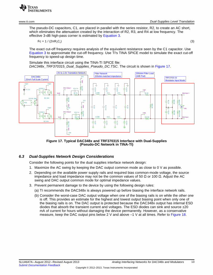
The pseudo-DC capacitors, C1, are placed in parallel with the series resistor, R2, to create an AC short,which eliminates the attenuation created by the interaction of R2, R3, and R4 at low frequency. Theeffective 3-dB high-pass corner is estimated by Equation 3.
Fc = 1 / (2πR2C1) (3)
The exact cut-off frequency requires analysis of the equivalent resistance seen by the C1 capacitor. UseEquation 3 to approximate the cut-off frequency. Use TI's TINA SPICE model to simulate the exact cut-offfrequency to speed-up design time.
Simulate this interface circuit using the TINA-TI SPICE file:DAC348x_TRF370315_Dual_Supplies_Pseudo_DC.TSC. The circuit is shown in Figure 17.
Figure 17. Typical DAC348x and TRF370315 Interface with Dual-Supplies(Pseudo-DC Network in TINA-TI)
6.3 Dual-Supplies Network Design ConsiderationsConsider the following points for the dual supplies interface network design:1. Maximize the AC swing by keeping the DAC output common mode as close to 0 V as possible.2. Depending on the available power supply rails and required bias common-mode voltage, the source
impedance and load impedance may not be the common values of 50 Ω or 100 Ω. Adjust the ACswing and DAC output common mode for optimal impedance values.
3. Prevent permanent damage to the device by using the following design rules:(a) TI recommends the DAC348x is always powered up before biasing the interface network rails.(b) Consider the worst-case DAC output voltage when one of the biasing rails is on while the other one
is off. This provides an estimate for the highest and lowest output biasing point when only one ofthe biasing rails is on. The DAC output is protected because the DAC348x output has internal ESDdiodes that absorb the transient current and voltages. The ESD diodes can sink and source ±20mA of current for hours without damaging the device permanently. However, as a conservativemeasure, keep the DAC output pins below 2 V and above –1 V at all times. Refer to Figure 18.
13SLUA647A–August 2012–Revised August 2013 Analog Interfacing Networks for DAC348x and ModulatorsSubmit Documentation Feedback
Copyright © 2012–2013, Texas Instruments Incorporated
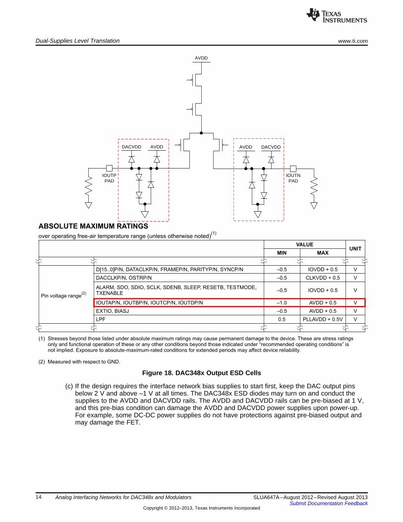
VALUEUNIT
MIN MAX
Pin voltage range(2)
D[15..0]P/N, DATACLKP/N, FRAMEP/N, PARITYP/N, SYNCP/N –0.5 IOVDD + 0.5 V
DACCLKP/N, OSTRP/N –0.5 CLKVDD + 0.5 V
ALARM, SDO, SDIO, SCLK, SDENB, SLEEP, RESETB, TESTMODE,TXENABLE
–0.5 IOVDD + 0.5 V
IOUTAP/N, IOUTBP/N, IOUTCP/N, IOUTDP/N –1.0 AVDD + 0.5 V
EXTIO, BIASJ –0.5 AVDD + 0.5 V
LPF 0.5 PLLAVDD + 0.5V V
over operating free-air temperature range (unless otherwise noted)(1)
(1) Stresses beyond those listed under absolute maximum ratings may cause permanent damage to the device. These are stress ratingsonly and functional operation of these or any other conditions beyond those indicated under “recommended operating conditions” isnot implied. Exposure to absolute-maximum-rated conditions for extended periods may affect device reliability.
(2) Measured with respect to GND.
ABSOLUTE MAXIMUM RATINGS
IOUTNPAD
AVDD
IOUTPPAD
AVDD DACVDDAVDDDACVDD
Dual-Supplies Level Translation www.ti.com
Figure 18. DAC348x Output ESD Cells
(c) If the design requires the interface network bias supplies to start first, keep the DAC output pinsbelow 2 V and above –1 V at all times. The DAC348x ESD diodes may turn on and conduct thesupplies to the AVDD and DACVDD rails. The AVDD and DACVDD rails can be pre-biased at 1 V,and this pre-bias condition can damage the AVDD and DACVDD power supplies upon power-up.For example, some DC-DC power supplies do not have protections against pre-biased output andmay damage the FET.
14 Analog Interfacing Networks for DAC348x and Modulators SLUA647A–August 2012–Revised August 2013Submit Documentation Feedback
Copyright © 2012–2013, Texas Instruments Incorporated
TRF372017
�
LO
DAC348x
IOUTA
IOUTB
SourceTermination
LoadTermination
VMOD
1:1
100
50 �
50 �
VDAC
1:1
100
www.ti.com AC-Coupled Network
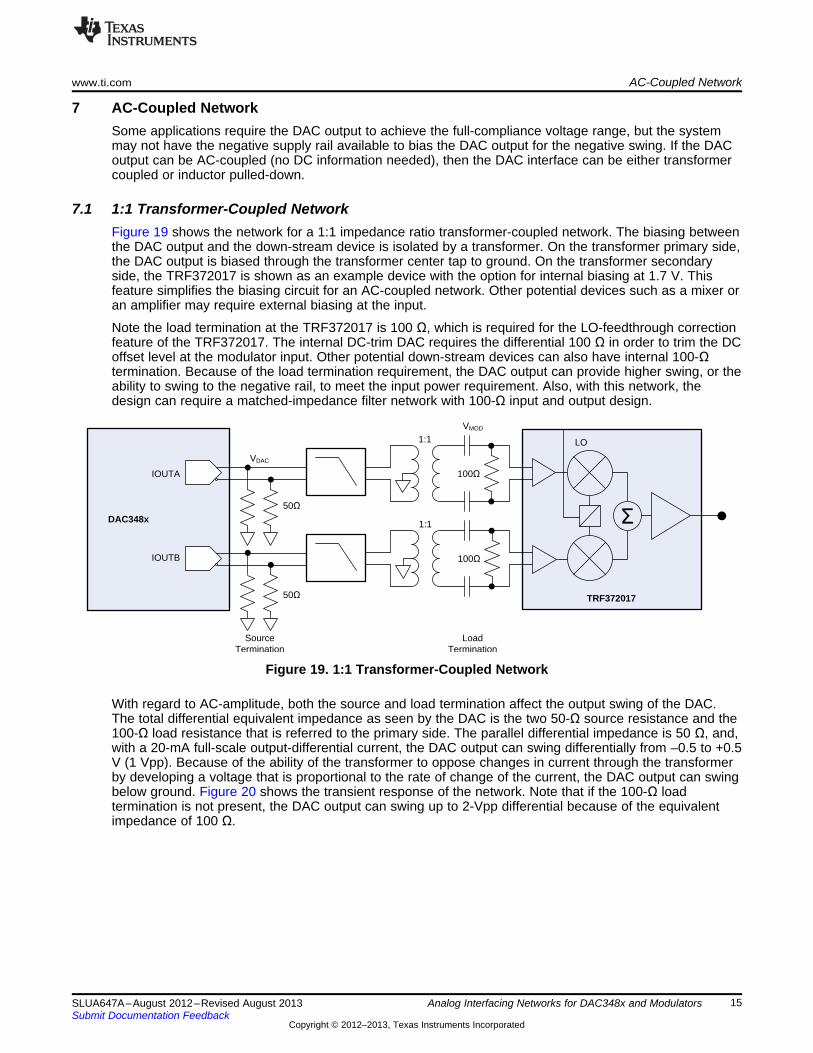
7 AC-Coupled NetworkSome applications require the DAC output to achieve the full-compliance voltage range, but the systemmay not have the negative supply rail available to bias the DAC output for the negative swing. If the DACoutput can be AC-coupled (no DC information needed), then the DAC interface can be either transformercoupled or inductor pulled-down.
7.1 1:1 Transformer-Coupled NetworkFigure 19 shows the network for a 1:1 impedance ratio transformer-coupled network. The biasing betweenthe DAC output and the down-stream device is isolated by a transformer. On the transformer primary side,the DAC output is biased through the transformer center tap to ground. On the transformer secondaryside, the TRF372017 is shown as an example device with the option for internal biasing at 1.7 V. Thisfeature simplifies the biasing circuit for an AC-coupled network. Other potential devices such as a mixer oran amplifier may require external biasing at the input.
Note the load termination at the TRF372017 is 100 Ω, which is required for the LO-feedthrough correctionfeature of the TRF372017. The internal DC-trim DAC requires the differential 100 Ω in order to trim the DCoffset level at the modulator input. Other potential down-stream devices can also have internal 100-Ωtermination. Because of the load termination requirement, the DAC output can provide higher swing, or theability to swing to the negative rail, to meet the input power requirement. Also, with this network, thedesign can require a matched-impedance filter network with 100-Ω input and output design.
Figure 19. 1:1 Transformer-Coupled Network
With regard to AC-amplitude, both the source and load termination affect the output swing of the DAC.The total differential equivalent impedance as seen by the DAC is the two 50-Ω source resistance and the100-Ω load resistance that is referred to the primary side. The parallel differential impedance is 50 Ω, and,with a 20-mA full-scale output-differential current, the DAC output can swing differentially from –0.5 to +0.5V (1 Vpp). Because of the ability of the transformer to oppose changes in current through the transformerby developing a voltage that is proportional to the rate of change of the current, the DAC output can swingbelow ground. Figure 20 shows the transient response of the network. Note that if the 100-Ω loadtermination is not present, the DAC output can swing up to 2-Vpp differential because of the equivalentimpedance of 100 Ω.
15SLUA647A–August 2012–Revised August 2013 Analog Interfacing Networks for DAC348x and ModulatorsSubmit Documentation Feedback
Copyright © 2012–2013, Texas Instruments Incorporated
3p3A3p3A
3p3A
-
+
VCCS1 1
-
+
VCCS2 1
IS1 10mA
IS2 10mA
-
+
-
+
VCVS1 10m
+
VG1
V1 3.3V
R1
100O
hm V+
VM1 N1
N2
N3
TRCT1 1
DAC Output+
Ioutp
Ioutn
DAC Output-
R9
50O
hmR
8 50
Ohm
1:1 Impedance Ratio Transformer
DAC348x20mA Full-Scale Current
20mA (0.25V)
IOUTAP
IOUTAN
10mA (0V)
0mA (í0.25V)
20mA (0.25V)
10mA (0V)
0mA (í0.25V)
0.5V
0V
í0.5V
IOUTA(Differential)
0.25V + VCM_MOD
BBIP
BBIN
VCM_MOD
í0.25V + VCM_MOD
0.25V + VCM_MOD
VCM_MOD
í0.25V + VCM_MOD
0.5V
0V
í0.5V
BBI(Differential)
AC-Coupled Network www.ti.com
Figure 20. 1:1 Transformer-Coupled Network Transient Response
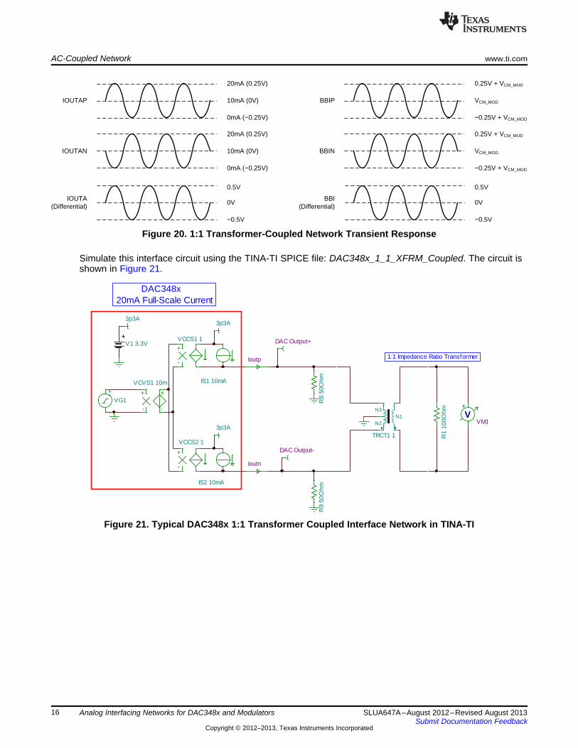
Simulate this interface circuit using the TINA-TI SPICE file: DAC348x_1_1_XFRM_Coupled. The circuit isshown in Figure 21.
Figure 21. Typical DAC348x 1:1 Transformer Coupled Interface Network in TINA-TI
16 Analog Interfacing Networks for DAC348x and Modulators SLUA647A–August 2012–Revised August 2013Submit Documentation Feedback
Copyright © 2012–2013, Texas Instruments Incorporated
20mA (0.5V)
IOUTAP
IOUTAN
10mA (0V)
0mA (í0.5V)
20mA (0.5V)
10mA (0V)
0mA (í0.5V)
1V
0V
í1V
IOUTA(Differential)
0.353V + VCM_MOD
BBIP
BBIN
VCM_MOD
í0.353V + VCM_MOD
0.353V + VCM_MOD
VCM_MOD
í0.353V + VCM_MOD
0.707V
0V
í0.707V
BBI(Differential)
TRF372017
�
LO
DAC348x
IOUTA
IOUTB
SourceTermination
LoadTermination
VMOD
2:1
100
100 �
100 �
VDAC
2:1
100
www.ti.com AC-Coupled Network
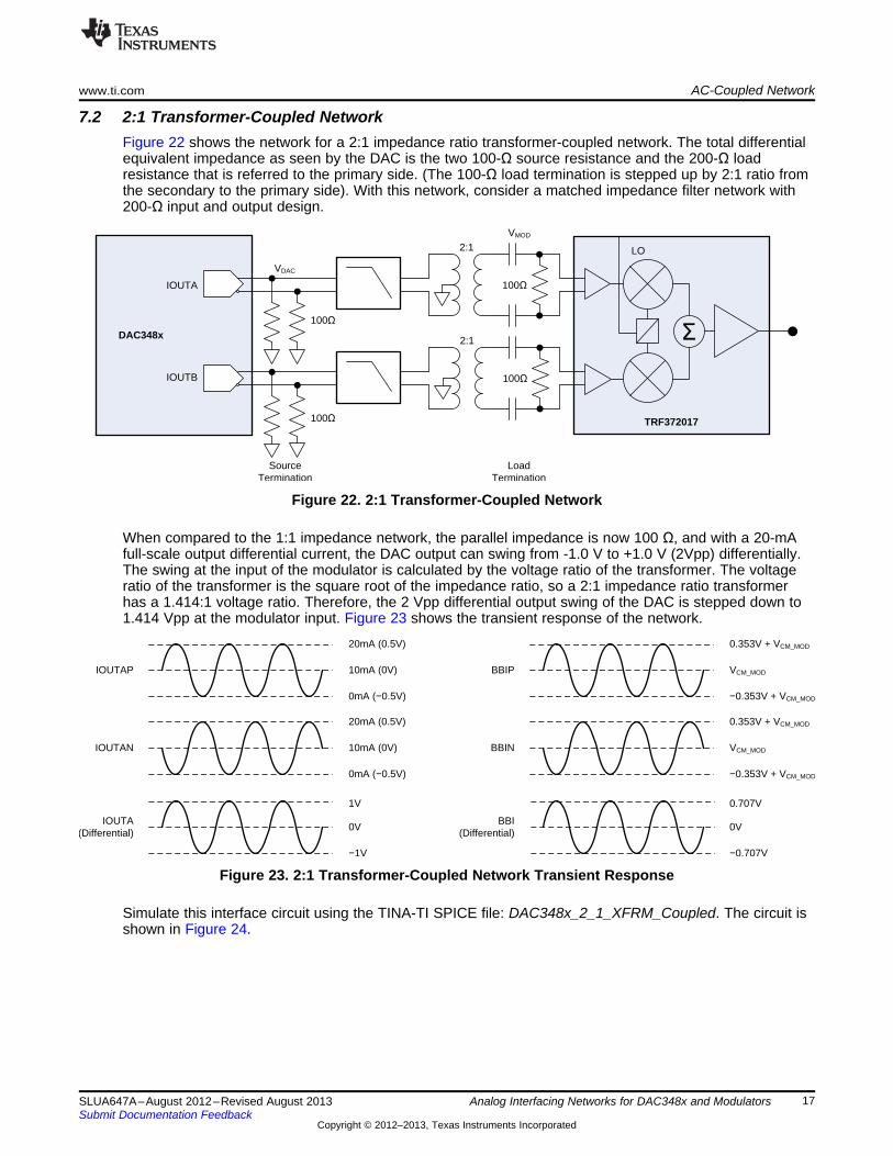
7.2 2:1 Transformer-Coupled NetworkFigure 22 shows the network for a 2:1 impedance ratio transformer-coupled network. The total differentialequivalent impedance as seen by the DAC is the two 100-Ω source resistance and the 200-Ω loadresistance that is referred to the primary side. (The 100-Ω load termination is stepped up by 2:1 ratio fromthe secondary to the primary side). With this network, consider a matched impedance filter network with200-Ω input and output design.
Figure 22. 2:1 Transformer-Coupled Network
When compared to the 1:1 impedance network, the parallel impedance is now 100 Ω, and with a 20-mAfull-scale output differential current, the DAC output can swing from -1.0 V to +1.0 V (2Vpp) differentially.The swing at the input of the modulator is calculated by the voltage ratio of the transformer. The voltageratio of the transformer is the square root of the impedance ratio, so a 2:1 impedance ratio transformerhas a 1.414:1 voltage ratio. Therefore, the 2 Vpp differential output swing of the DAC is stepped down to1.414 Vpp at the modulator input. Figure 23 shows the transient response of the network.
Figure 23. 2:1 Transformer-Coupled Network Transient Response
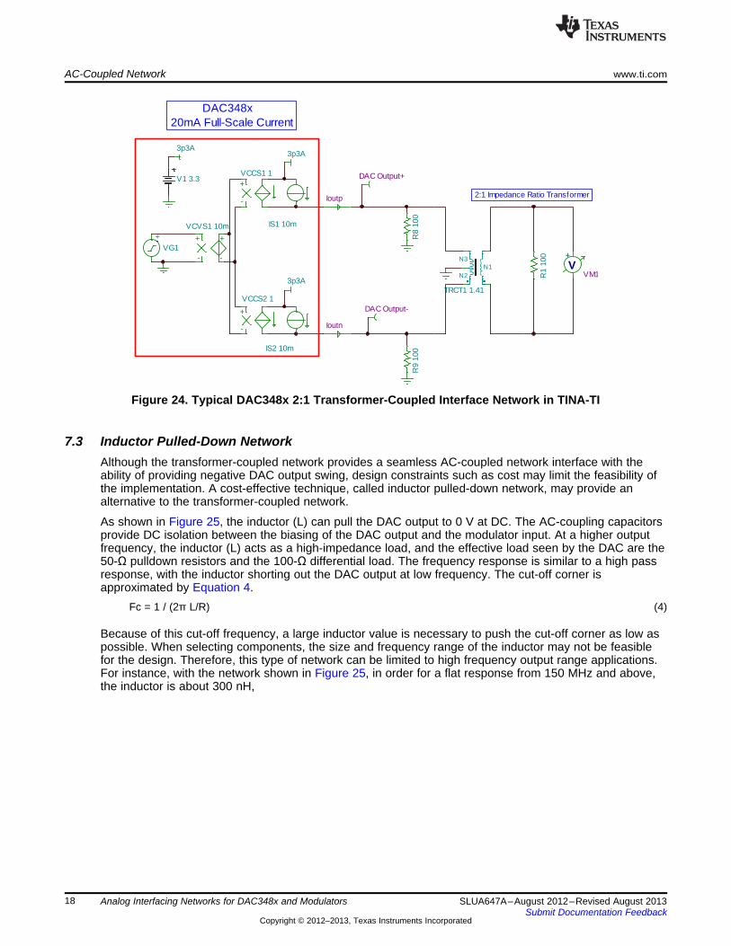
Simulate this interface circuit using the TINA-TI SPICE file: DAC348x_2_1_XFRM_Coupled. The circuit isshown in Figure 24.
17SLUA647A–August 2012–Revised August 2013 Analog Interfacing Networks for DAC348x and ModulatorsSubmit Documentation Feedback
Copyright © 2012–2013, Texas Instruments Incorporated
3p3A3p3A
3p3A
-
+VCCS1 1
-
+
VCCS2 1
IS1 10m
IS2 10m
-
+
-
+
VCVS1 10m
+
VG1
V1 3.3 DAC Output+
Ioutp
Ioutn
DAC Output-
R9
100
R8
100
R1
100
V+
VM1N1
N2
N3
TRCT1 1.41
2:1 Impedance Ratio Transformer
DAC348x20mA Full-Scale Current
AC-Coupled Network www.ti.com
Figure 24. Typical DAC348x 2:1 Transformer-Coupled Interface Network in TINA-TI
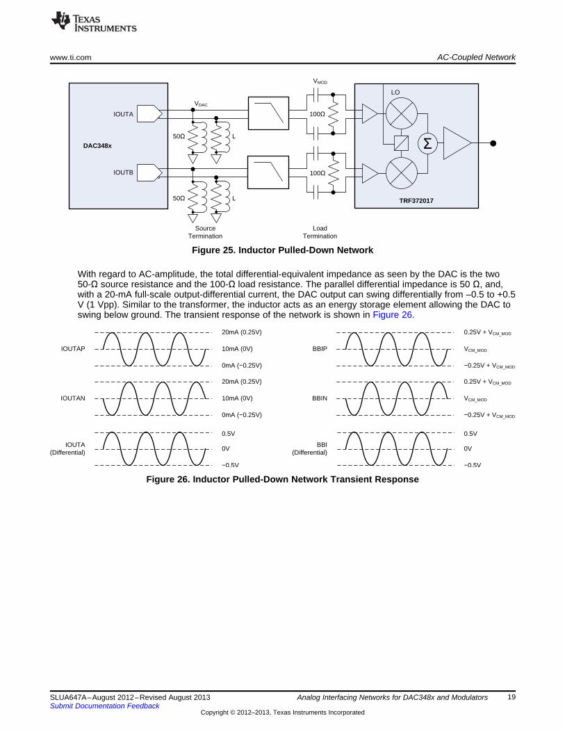
7.3 Inductor Pulled-Down NetworkAlthough the transformer-coupled network provides a seamless AC-coupled network interface with theability of providing negative DAC output swing, design constraints such as cost may limit the feasibility ofthe implementation. A cost-effective technique, called inductor pulled-down network, may provide analternative to the transformer-coupled network.
As shown in Figure 25, the inductor (L) can pull the DAC output to 0 V at DC. The AC-coupling capacitorsprovide DC isolation between the biasing of the DAC output and the modulator input. At a higher outputfrequency, the inductor (L) acts as a high-impedance load, and the effective load seen by the DAC are the50-Ω pulldown resistors and the 100-Ω differential load. The frequency response is similar to a high passresponse, with the inductor shorting out the DAC output at low frequency. The cut-off corner isapproximated by Equation 4.
Fc = 1 / (2π L/R) (4)
Because of this cut-off frequency, a large inductor value is necessary to push the cut-off corner as low aspossible. When selecting components, the size and frequency range of the inductor may not be feasiblefor the design. Therefore, this type of network can be limited to high frequency output range applications.For instance, with the network shown in Figure 25, in order for a flat response from 150 MHz and above,the inductor is about 300 nH,
18 Analog Interfacing Networks for DAC348x and Modulators SLUA647A–August 2012–Revised August 2013Submit Documentation Feedback
Copyright © 2012–2013, Texas Instruments Incorporated
20mA (0.25V)
IOUTAP
IOUTAN
10mA (0V)
0mA (í0.25V)
20mA (0.25V)
10mA (0V)
0mA (í0.25V)
0.5V
0V
í0.5V
IOUTA(Differential)
0.25V + VCM_MOD
BBIP
BBIN
VCM_MOD
í0.25V + VCM_MOD
0.25V + VCM_MOD
VCM_MOD
í0.25V + VCM_MOD
0.5V
0V
í0.5V
BBI(Differential)
TRF372017
�
LO
DAC348x
IOUTA
IOUTB
SourceTermination
LoadTermination
VMOD
100
50 �
50 �
VDAC
100
L
L
www.ti.com AC-Coupled Network
Figure 25. Inductor Pulled-Down Network
With regard to AC-amplitude, the total differential-equivalent impedance as seen by the DAC is the two50-Ω source resistance and the 100-Ω load resistance. The parallel differential impedance is 50 Ω, and,with a 20-mA full-scale output-differential current, the DAC output can swing differentially from –0.5 to +0.5V (1 Vpp). Similar to the transformer, the inductor acts as an energy storage element allowing the DAC toswing below ground. The transient response of the network is shown in Figure 26.
Figure 26. Inductor Pulled-Down Network Transient Response
19SLUA647A–August 2012–Revised August 2013 Analog Interfacing Networks for DAC348x and ModulatorsSubmit Documentation Feedback
Copyright © 2012–2013, Texas Instruments Incorporated
3p3A3p3A
3p3A
-
+
VCCS1 1
-
+
VCCS2 1
IS1 10m
IS2 10m
-
+
-
+
VCVS1 10m
+
VG1
V1 3.3
V+
VM1
DAC Output+
Ioutp
Ioutn
DAC Output-R
9 50
R8
50
R1
100
R2
1T
R3
1T
L2 3
00n
L1 3
00n
C1 1u
C2 1u
L3 21n
C3
1.6p
L4 21n
L5 21n
C4
5.3p
L6 21n
C5
1.6p
AM
1 A
M2
V+
VM2
Mixer Input Model
1T ohm resistor used to aid SPICE simulation bias
5th Order Butterworth LPFCutoff = 600MHz
Inductor to bias the DAC output to 0V
DAC348x20mA Full-Scale Current
Conclusion www.ti.com
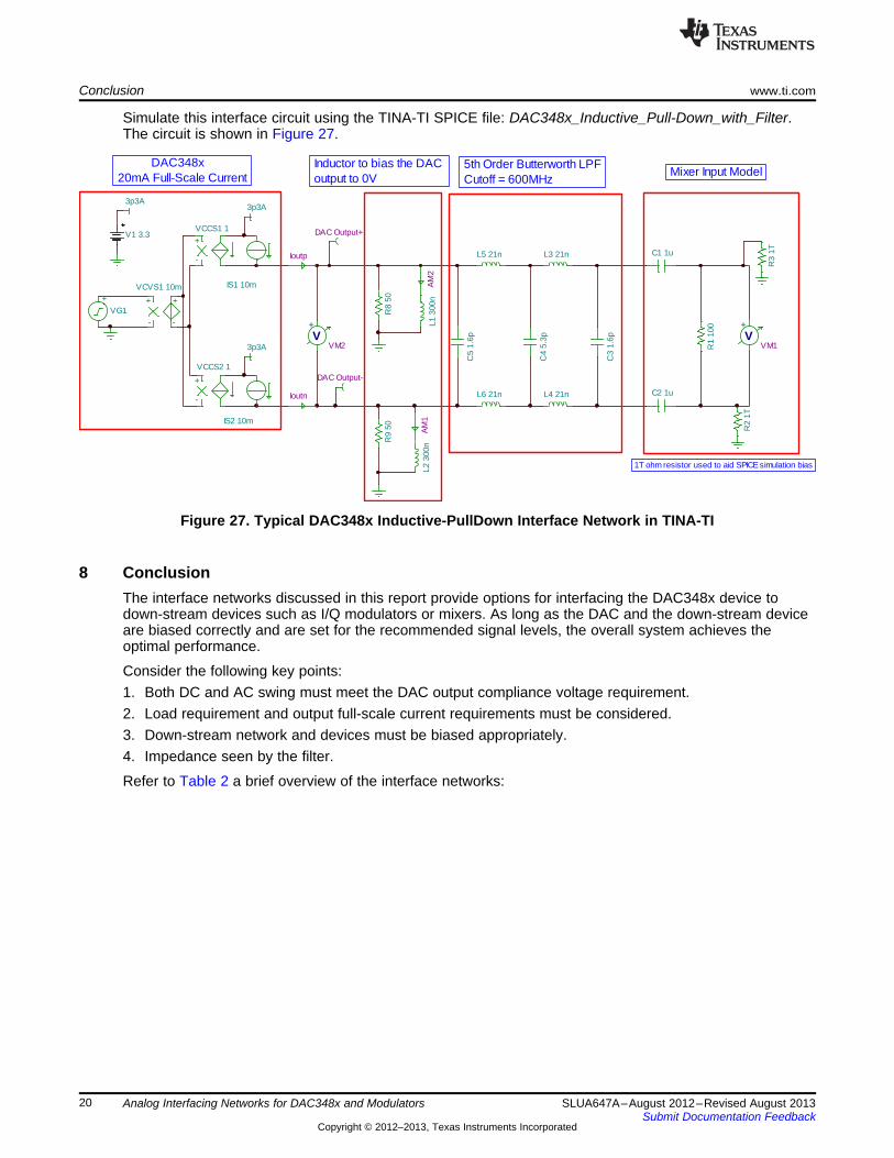
Simulate this interface circuit using the TINA-TI SPICE file: DAC348x_Inductive_Pull-Down_with_Filter.The circuit is shown in Figure 27.
Figure 27. Typical DAC348x Inductive-PullDown Interface Network in TINA-TI
8 ConclusionThe interface networks discussed in this report provide options for interfacing the DAC348x device todown-stream devices such as I/Q modulators or mixers. As long as the DAC and the down-stream deviceare biased correctly and are set for the recommended signal levels, the overall system achieves theoptimal performance.
Consider the following key points:1. Both DC and AC swing must meet the DAC output compliance voltage requirement.2. Load requirement and output full-scale current requirements must be considered.3. Down-stream network and devices must be biased appropriately.4. Impedance seen by the filter.
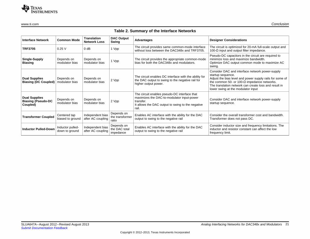
Refer to Table 2 a brief overview of the interface networks:
20 Analog Interfacing Networks for DAC348x and Modulators SLUA647A–August 2012–Revised August 2013Submit Documentation Feedback
Copyright © 2012–2013, Texas Instruments Incorporated
www.ti.com Conclusion
Table 2. Summary of the Interface Networks
Translation DAC OutputInterface Network Common Mode Advantages Designer ConsiderationsNetwork Loss SwingThe circuit provides same common-mode interface The circuit is optimized for 20-mA full-scale output andTRF3705 0.25 V 0 dB 1 Vpp without loss between the DAC348x and TRF3705. 100-Ω input and output filter impedance.
Pseudo-DC capacitors in the circuit are required toSingle-Supply Depends on Depends on The circuit provides the appropriate common-mode minimize loss and maximize bandwidth.1 VppBiasing modulator bias modulator bias bias for both the DAC348x and modulators. Optimize DAC output common mode to maximize AC
swing.Consider DAC and interface network power-supplystartup sequence.The circuit enables DC interface with the ability forDual Supplies Depends on Depends on Adjust the bias level and power supply rails for some of2 Vpp the DAC output to swing to the negative rail forBiasing (DC Coupled) modulator bias modulator bias the common 50- or 100-Ω impedance networks.higher output power. The translation network can create loss and result inlower swing at the modulator input
The circuit enables pseudo-DC interface thatDual Supplies maximizes the DAC-to-modulator input-powerDepends on Depends on Consider DAC and interface network power-supplyBiasing (Pseudo-DC 2 Vpp transfer.modulator bias modulator bias startup sequence.Coupled) It allows the DAC output to swing to the negative
rail.Depends onCentered tap Independent bias Enables AC interface with the ability for the DAC Consider the overall transformer cost and bandwidth.Transformer Coupled the transformerbiased to ground after AC coupling output to swing to the negative rail Transformer does not pass DC.ratioDepends on Consider inductor size and frequency limitations. TheInductor pulled- Independent bias Enables AC interface with the ability for the DACInductor Pulled-Down the DAC total inductor and resistor constant can affect the lowdown to ground after AC coupling output to swing to the negative railimpedance frequency limit.
21SLUA647A–August 2012–Revised August 2013 Analog Interfacing Networks for DAC348x and ModulatorsSubmit Documentation Feedback
Copyright © 2012–2013, Texas Instruments Incorporated
References www.ti.com
9 References1. Getting Started with TINA-TI, SBOU0522. TINA-TI Spice files, SLUC4813. DAC3482 datasheet, Dual-Channel, 16-Bit, 1.25 GSPS Digital-to-Analog Converter (DAC), SLAS7484. DAC3484 datasheet, Quad-Channel, 16-Bit, 1.25 GSPS Digital-to-Analog Converter (DAC), SLAS7495. DAC34H84 datasheet, Quad-Channel, 16-Bit, 1.25 GSPS Digital-to-Analog Converter (DAC), SLAS7516. DAC34SH84 datasheet, Quad-Channel, 16-Bit, 1.5 GSPS Digital-to-Analog Converter (DAC),
SLAS808
10 About the AuthorKang Hsia is an Applications Engineer in the High Speed Data Converters group at Texas Instruments. Heprimarily provides customer support for TI's high-speed ADCs and DACs. Prior to joining TI in 2007, Kangearned his bachelor of science in electrical engineering from California Polytechnic State University (CalPoly) in San Luis Obispo, California. Kang is an active member of the TI E2E™ Community, and can bereached through e2e.ti.com for support.
22 Analog Interfacing Networks for DAC348x and Modulators SLUA647A–August 2012–Revised August 2013Submit Documentation Feedback
Copyright © 2012–2013, Texas Instruments Incorporated

IMPORTANT NOTICE FOR TI REFERENCE DESIGNSTexas Instruments Incorporated ("TI") reference designs are solely intended to assist designers (“Buyers”) who are developing systems thatincorporate TI semiconductor products (also referred to herein as “components”). Buyer understands and agrees that Buyer remainsresponsible for using its independent analysis, evaluation and judgment in designing Buyer’s systems and products.TI reference designs have been created using standard laboratory conditions and engineering practices. TI has not conducted anytesting other than that specifically described in the published documentation for a particular reference design. TI may makecorrections, enhancements, improvements and other changes to its reference designs.Buyers are authorized to use TI reference designs with the TI component(s) identified in each particular reference design and to modify thereference design in the development of their end products. HOWEVER, NO OTHER LICENSE, EXPRESS OR IMPLIED, BY ESTOPPELOR OTHERWISE TO ANY OTHER TI INTELLECTUAL PROPERTY RIGHT, AND NO LICENSE TO ANY THIRD PARTY TECHNOLOGYOR INTELLECTUAL PROPERTY RIGHT, IS GRANTED HEREIN, including but not limited to any patent right, copyright, mask work right,or other intellectual property right relating to any combination, machine, or process in which TI components or services are used.Information published by TI regarding third-party products or services does not constitute a license to use such products or services, or awarranty or endorsement thereof. Use of such information may require a license from a third party under the patents or other intellectualproperty of the third party, or a license from TI under the patents or other intellectual property of TI.TI REFERENCE DESIGNS ARE PROVIDED "AS IS". TI MAKES NO WARRANTIES OR REPRESENTATIONS WITH REGARD TO THEREFERENCE DESIGNS OR USE OF THE REFERENCE DESIGNS, EXPRESS, IMPLIED OR STATUTORY, INCLUDING ACCURACY ORCOMPLETENESS. TI DISCLAIMS ANY WARRANTY OF TITLE AND ANY IMPLIED WARRANTIES OF MERCHANTABILITY, FITNESSFOR A PARTICULAR PURPOSE, QUIET ENJOYMENT, QUIET POSSESSION, AND NON-INFRINGEMENT OF ANY THIRD PARTYINTELLECTUAL PROPERTY RIGHTS WITH REGARD TO TI REFERENCE DESIGNS OR USE THEREOF. TI SHALL NOT BE LIABLEFOR AND SHALL NOT DEFEND OR INDEMNIFY BUYERS AGAINST ANY THIRD PARTY INFRINGEMENT CLAIM THAT RELATES TOOR IS BASED ON A COMBINATION OF COMPONENTS PROVIDED IN A TI REFERENCE DESIGN. IN NO EVENT SHALL TI BELIABLE FOR ANY ACTUAL, SPECIAL, INCIDENTAL, CONSEQUENTIAL OR INDIRECT DAMAGES, HOWEVER CAUSED, ON ANYTHEORY OF LIABILITY AND WHETHER OR NOT TI HAS BEEN ADVISED OF THE POSSIBILITY OF SUCH DAMAGES, ARISING INANY WAY OUT OF TI REFERENCE DESIGNS OR BUYER’S USE OF TI REFERENCE DESIGNS.TI reserves the right to make corrections, enhancements, improvements and other changes to its semiconductor products and services perJESD46, latest issue, and to discontinue any product or service per JESD48, latest issue. Buyers should obtain the latest relevantinformation before placing orders and should verify that such information is current and complete. All semiconductor products are soldsubject to TI’s terms and conditions of sale supplied at the time of order acknowledgment.TI warrants performance of its components to the specifications applicable at the time of sale, in accordance with the warranty in TI’s termsand conditions of sale of semiconductor products. Testing and other quality control techniques for TI components are used to the extent TIdeems necessary to support this warranty. Except where mandated by applicable law, testing of all parameters of each component is notnecessarily performed.TI assumes no liability for applications assistance or the design of Buyers’ products. Buyers are responsible for their products andapplications using TI components. To minimize the risks associated with Buyers’ products and applications, Buyers should provideadequate design and operating safeguards.Reproduction of significant portions of TI information in TI data books, data sheets or reference designs is permissible only if reproduction iswithout alteration and is accompanied by all associated warranties, conditions, limitations, and notices. TI is not responsible or liable forsuch altered documentation. Information of third parties may be subject to additional restrictions.Buyer acknowledges and agrees that it is solely responsible for compliance with all legal, regulatory and safety-related requirementsconcerning its products, and any use of TI components in its applications, notwithstanding any applications-related information or supportthat may be provided by TI. Buyer represents and agrees that it has all the necessary expertise to create and implement safeguards thatanticipate dangerous failures, monitor failures and their consequences, lessen the likelihood of dangerous failures and take appropriateremedial actions. Buyer will fully indemnify TI and its representatives against any damages arising out of the use of any TI components inBuyer’s safety-critical applications.In some cases, TI components may be promoted specifically to facilitate safety-related applications. With such components, TI’s goal is tohelp enable customers to design and create their own end-product solutions that meet applicable functional safety standards andrequirements. Nonetheless, such components are subject to these terms.No TI components are authorized for use in FDA Class III (or similar life-critical medical equipment) unless authorized officers of the partieshave executed an agreement specifically governing such use.Only those TI components that TI has specifically designated as military grade or “enhanced plastic” are designed and intended for use inmilitary/aerospace applications or environments. Buyer acknowledges and agrees that any military or aerospace use of TI components thathave not been so designated is solely at Buyer's risk, and Buyer is solely responsible for compliance with all legal and regulatoryrequirements in connection with such use.TI has specifically designated certain components as meeting ISO/TS16949 requirements, mainly for automotive use. In any case of use ofnon-designated products, TI will not be responsible for any failure to meet ISO/TS16949.
Mailing Address: Texas Instruments, Post Office Box 655303, Dallas, Texas 75265Copyright © 2013, Texas Instruments Incorporated