Analog IC Design (ETIN25) Lab1 Laboratory Manual - LTH · Laboratory 1: Cadence, DC parameters and...
33
Electrical and Information Technology LTH Analog IC Design (ETIN25) Lab1 Laboratory Manual Henrik Sjöland Jonas Lindstrand Martin Liliebladh Markus Törmänen October 2016
Transcript of Analog IC Design (ETIN25) Lab1 Laboratory Manual - LTH · Laboratory 1: Cadence, DC parameters and...
Electr ica l and In format ion Technology LTH
Analog IC Design (ETIN25)
Lab1 Laboratory Manual
Henrik Sjöland
Jonas Lindstrand
Martin Liliebladh
Markus Törmänen
October 2016
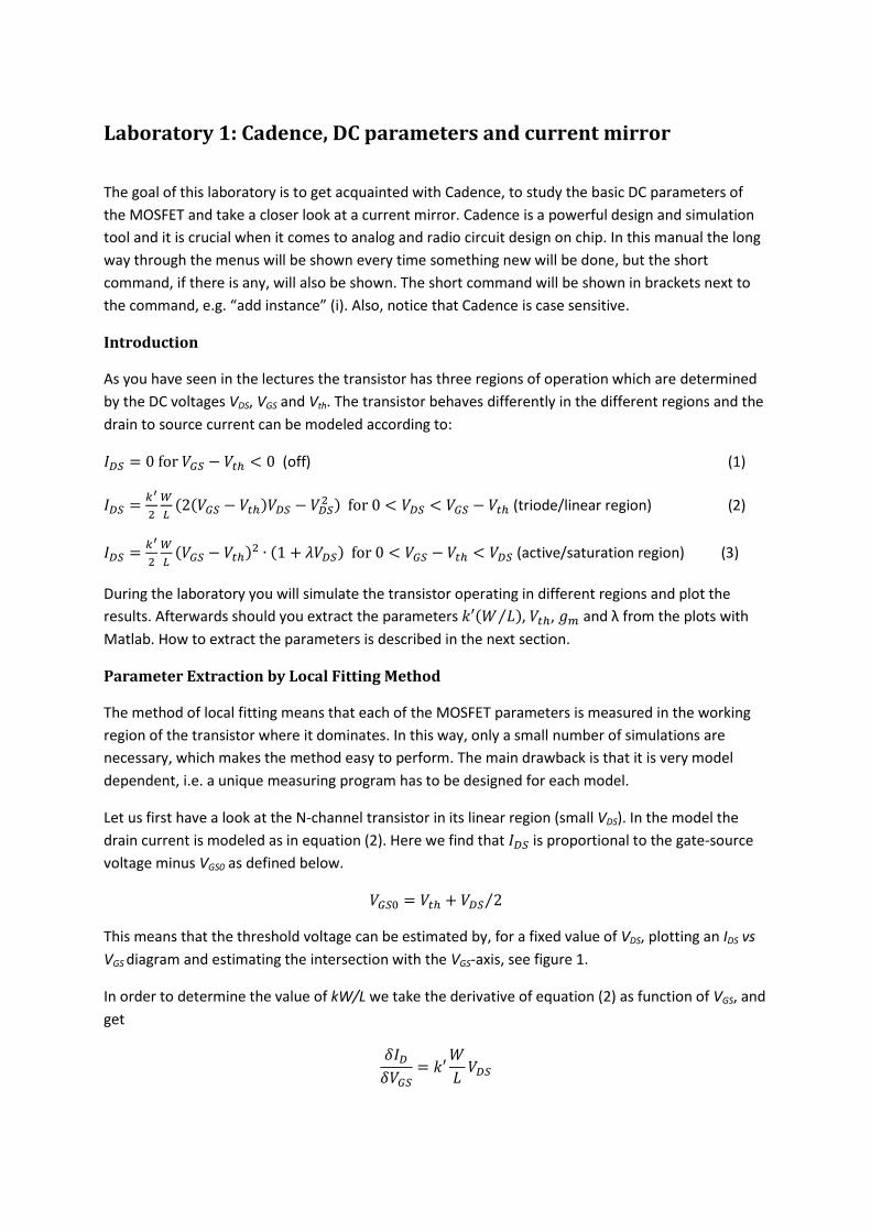
Laboratory 1: Cadence, DC parameters and current mirror
The goal of this laboratory is to get acquainted with Cadence, to study the basic DC parameters of
the MOSFET and take a closer look at a current mirror. Cadence is a powerful design and simulation
tool and it is crucial when it comes to analog and radio circuit design on chip. In this manual the long
way through the menus will be shown every time something new will be done, but the short
command, if there is any, will also be shown. The short command will be shown in brackets next to
the command, e.g. “add instance” (i). Also, notice that Cadence is case sensitive.
Introduction
As you have seen in the lectures the transistor has three regions of operation which are determined
by the DC voltages VDS, VGS and Vth. The transistor behaves differently in the different regions and the
drain to source current can be modeled according to:
𝐼𝐷𝑆 = 0 for 𝑉𝐺𝑆 − 𝑉𝑡ℎ < 0 (off) (1)
𝐼𝐷𝑆 =𝑘′
2
𝑊
𝐿(2(𝑉𝐺𝑆 − 𝑉𝑡ℎ)𝑉𝐷𝑆 − 𝑉𝐷𝑆
2 ) for 0 < 𝑉𝐷𝑆 < 𝑉𝐺𝑆 − 𝑉𝑡ℎ (triode/linear region) (2)
𝐼𝐷𝑆 =𝑘′
2
𝑊
𝐿(𝑉𝐺𝑆 − 𝑉𝑡ℎ)2 ∙ (1 + 𝜆𝑉𝐷𝑆) for 0 < 𝑉𝐺𝑆 − 𝑉𝑡ℎ < 𝑉𝐷𝑆 (active/saturation region) (3)
During the laboratory you will simulate the transistor operating in different regions and plot the
results. Afterwards should you extract the parameters 𝑘′(𝑊 𝐿⁄ ), 𝑉𝑡ℎ, 𝑔𝑚 and λ from the plots with
Matlab. How to extract the parameters is described in the next section.
Parameter Extraction by Local Fitting Method
The method of local fitting means that each of the MOSFET parameters is measured in the working
region of the transistor where it dominates. In this way, only a small number of simulations are
necessary, which makes the method easy to perform. The main drawback is that it is very model
dependent, i.e. a unique measuring program has to be designed for each model.
Let us first have a look at the N-channel transistor in its linear region (small VDS). In the model the
drain current is modeled as in equation (2). Here we find that 𝐼𝐷𝑆 is proportional to the gate-source
voltage minus VGS0 as defined below.
𝑉𝐺𝑆0 = 𝑉𝑡ℎ + 𝑉𝐷𝑆 2⁄
This means that the threshold voltage can be estimated by, for a fixed value of VDS, plotting an IDS vs
VGS diagram and estimating the intersection with the VGS-axis, see figure 1.
In order to determine the value of kW/L we take the derivative of equation (2) as function of VGS, and
get
𝛿𝐼𝐷
𝛿𝑉𝐺𝑆= 𝑘′
𝑊
𝐿𝑉𝐷𝑆
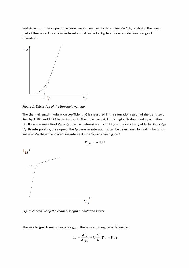
and since this is the slope of the curve, we can now easily determine kW/L by analyzing the linear
part of the curve. It is advisable to set a small value for VDS to achieve a wide linear range of
operation.
Figure 1: Extraction of the threshold voltage.
The channel length modulation coefficient (λ) is measured in the saturation region of the transistor.
See Eq. 1.164 and 1.165 in the textbook. The drain current, in this region, is described by equation
(3). If we assume a fixed VGS > Vth , we can determine λ by looking at the sensitivity of IDS for VDS > VGS-
Vth. By interpolating the slope of the IDS curve in saturation, λ can be determined by finding for which
value of VDS the extrapolated line intercepts the VDS-axis. See figure 2.
𝑉𝐷𝑆0 = − 1 𝜆⁄
Figure 2: Measuring the channel length modulation factor.
The small-signal transconductance gm in the saturation region is defined as
𝑔𝑚 =𝛿𝐼𝐷
𝛿𝑉𝐺𝑆≈ 𝑘′
𝑊
𝐿(𝑉𝐺𝑆 − 𝑉𝑡ℎ)
Homework
1. Read this manual carefully. It is recommended that you start Cadence and try to solve the
laboratory assignments before the laboratory..
2. Look at the section about Parameter Extraction by Local Fitting Method and prepare a
Matlab program that can extract the parameters when you have got the data from the
laboratory session.
3. Calculate the following parameters: gm, CGS, IDS and ft. Use parameters from the 65nm
datasheet used in this course (found on the Analog IC course website) and the following
values: W = 10µm, L = 0.2µm, VGS = 600mV, VDS = 50mV and VDS = 600mV
4. Explain in your own words how the current mirror works. Why is the current mirror used?
5. Calculate the reference current (Iref) and width (W) of the transistors in a 1:1 PMOS current
mirror. The DC output resistance (rO) is 500kΩ and the drawn channel length is 1µm. All
transistors are in strong inversion with Vov=0.2V. Use the 65nm process parameters.
6. Explain why it is beneficial to have the transistors divided into an even number of fingers?
7. What is the definition for the output impedance of transistor?
Introduction to Cadence and simulation of a MOSFET’s DC parameters
Start a terminal window and create a folder for the laboratory sessions. Open the folder and initiate
Cadence with the command “inittde ana20xx”. When the terminal is ready type “virtuoso &” to start
Cadence, see figure 3.
Figure 3. Terminal window with the commands to create a directory and start Cadence.
Cadence will now open two windows, “icfb – Log:/…” and “Library Manager”. Cadence uses many
windows and it is not unusual to have six windows opened at the same time. To make it a bit easier
and to get a good overview one suggestion is to use more than one desktop. “icfb – Log:/…” is the
main window in that extent that if you close it or use the menu “File”-> ”Exit …” Cadence will shut
down. It also logs all the commands and activities you perform, you can always check here if
something is not working. “Library Manager”, see figure 4, shows the different libraries with their
content. A library contains different instances/circuit elements that can be used in your designs. You
will now create your own library that will be used during the laboratory sessions of this course. Go to
“File - > New -> Library” in the “Library Manger” window. Write a name for your library, e.g. analogIC,
and click “OK”. In the next window you choose “Attach to an existing techfile” and click “OK”. In the
list “Technology Library” choose “cmos065” and then “OK”. The library will now appear in the library
list in “Library Manager”.
inittde ana2016
virtuoso &
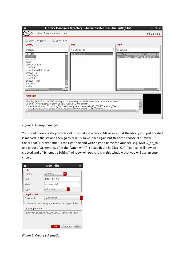
Figure 4. Library manager
You should now create you first cell or circuit in Cadence. Make sure that the library you just created
is marked in the list and then go to “File - > New” once again but this time choose “Cell View …”.
Check that “Library name” is the right one and write a good name for your cell, e.g. NMOS_dc_tb,
and choose “Schematics L” in the “Open with” list. See figure 5. Click “OK”. Your cell will now be
created and a “Schematic Editing” window will open. It is in this window that you will design your
circuit.
Figure 5. Create schematic.
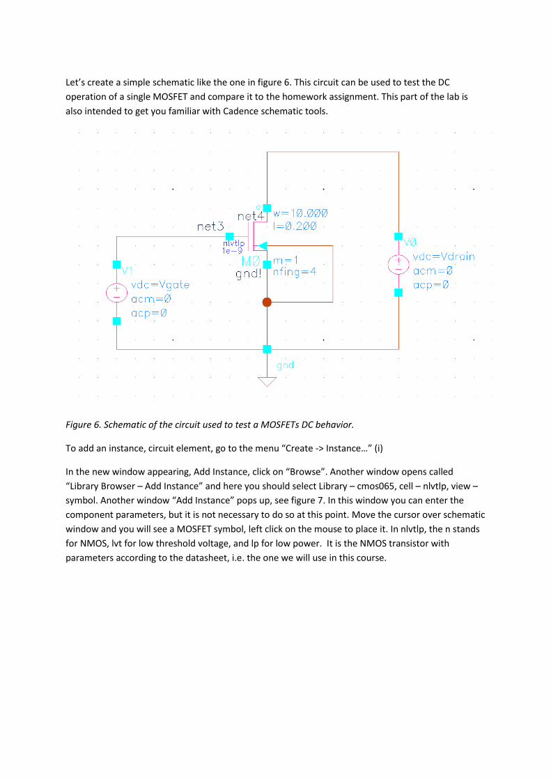
Let’s create a simple schematic like the one in figure 6. This circuit can be used to test the DC
operation of a single MOSFET and compare it to the homework assignment. This part of the lab is
also intended to get you familiar with Cadence schematic tools.
Figure 6. Schematic of the circuit used to test a MOSFETs DC behavior.
To add an instance, circuit element, go to the menu “Create -> Instance…” (i)
In the new window appearing, Add Instance, click on “Browse”. Another window opens called
“Library Browser – Add Instance” and here you should select Library – cmos065, cell – nlvtlp, view –
symbol. Another window “Add Instance” pops up, see figure 7. In this window you can enter the
component parameters, but it is not necessary to do so at this point. Move the cursor over schematic
window and you will see a MOSFET symbol, left click on the mouse to place it. In nlvtlp, the n stands
for NMOS, lvt for low threshold voltage, and lp for low power. It is the NMOS transistor with
parameters according to the datasheet, i.e. the one we will use in this course.
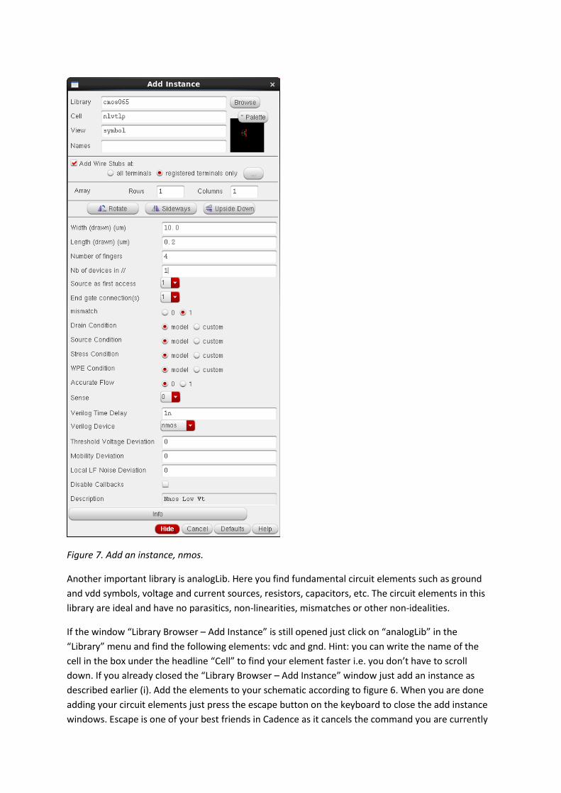
Figure 7. Add an instance, nmos.
Another important library is analogLib. Here you find fundamental circuit elements such as ground
and vdd symbols, voltage and current sources, resistors, capacitors, etc. The circuit elements in this
library are ideal and have no parasitics, non-linearities, mismatches or other non-idealities.
If the window “Library Browser – Add Instance” is still opened just click on “analogLib” in the
“Library” menu and find the following elements: vdc and gnd. Hint: you can write the name of the
cell in the box under the headline “Cell” to find your element faster i.e. you don’t have to scroll
down. If you already closed the “Library Browser – Add Instance” window just add an instance as
described earlier (i). Add the elements to your schematic according to figure 6. When you are done
adding your circuit elements just press the escape button on the keyboard to close the add instance
windows. Escape is one of your best friends in Cadence as it cancels the command you are currently

using, e.g. adding instances, wires or moving objects. Make it a habit to press it when you are done
with your latest command and get used to press the Esc button a lot.
Now you should add the wires. Go to the menu “Create->Wire (narrow)” (w)
Connect the elements by left clicking on the red contacts. You can also click anywhere in your
schematic window to fasten the wire there before continue to the next contact. If you want to move
a wire or element go to the menu “Edit->Move” (M) and then click on the object you want to move.
In the Edit menu you will also find useful commands as: undo (u), redo (U), stretch (m), copy (c),
delete (Delete) and rotate (right mouse click). The difference between move and stretch is that with
stretch the wires connected to the element will follow as you move the element and the connection
will not be broken, but with move the element will be moved out of the circuit.
When finished the schematic should look like the one in figure 6.
If you did not enter the proper parameters of the NMOS when creating it using the “Add Instance”
window of figure 7, you should now edit the properties of the NMOS. To edit the properties of an
instance go to the menu “Edit –> Properties –> Objects…” (q) and then click on the nmos. A new
window opens called “Edit Object Properties”. Take a look of the different properties that can be
changed. Edit the “Width”, “Length” and “Number of fingers” according to figure 8.
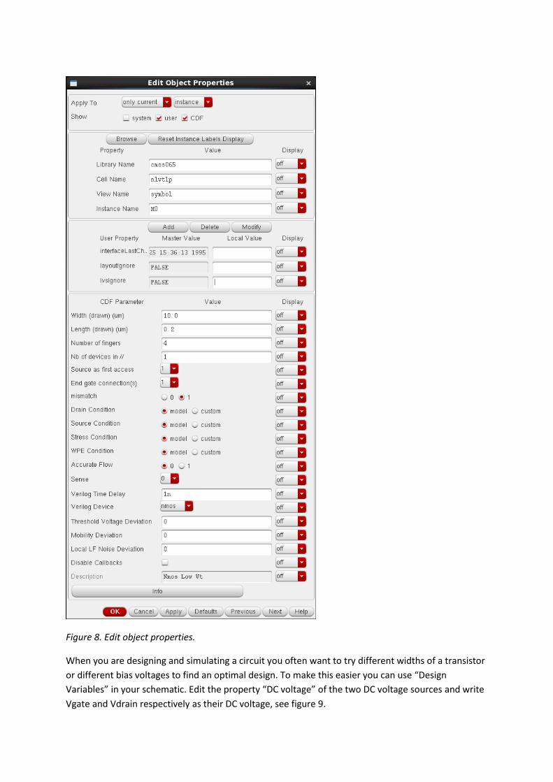
Figure 8. Edit object properties.
When you are designing and simulating a circuit you often want to try different widths of a transistor
or different bias voltages to find an optimal design. To make this easier you can use “Design
Variables” in your schematic. Edit the property “DC voltage” of the two DC voltage sources and write
Vgate and Vdrain respectively as their DC voltage, see figure 9.
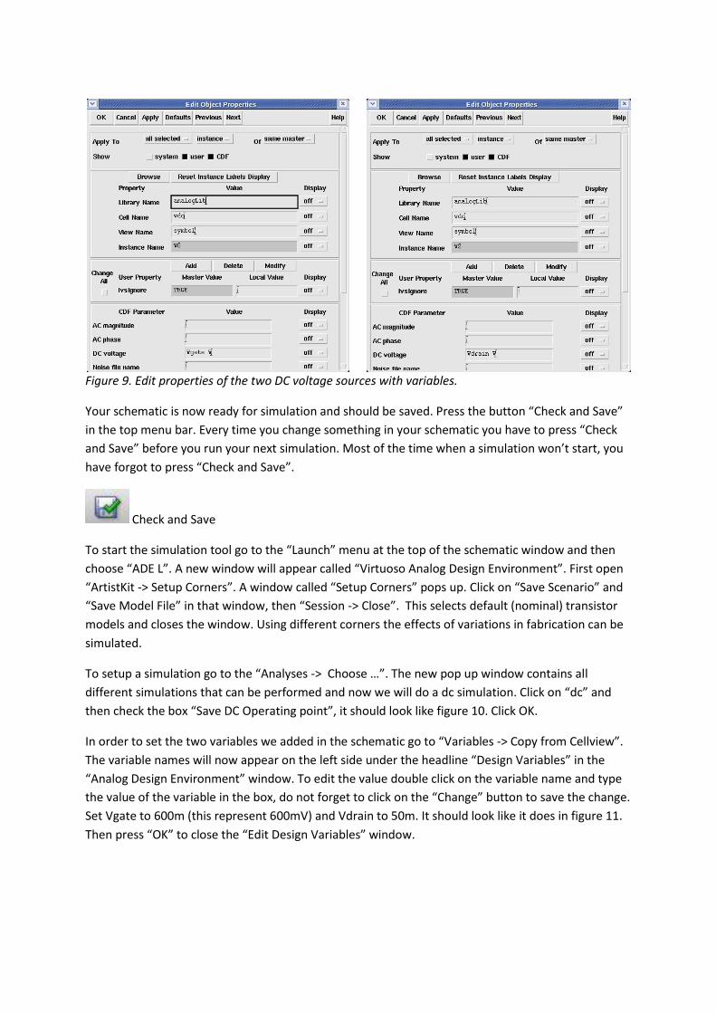
Figure 9. Edit properties of the two DC voltage sources with variables.
Your schematic is now ready for simulation and should be saved. Press the button “Check and Save”
in the top menu bar. Every time you change something in your schematic you have to press “Check
and Save” before you run your next simulation. Most of the time when a simulation won’t start, you
have forgot to press “Check and Save”.
Check and Save
To start the simulation tool go to the “Launch” menu at the top of the schematic window and then
choose “ADE L”. A new window will appear called “Virtuoso Analog Design Environment”. First open
“ArtistKit -> Setup Corners”. A window called “Setup Corners” pops up. Click on “Save Scenario” and
“Save Model File” in that window, then “Session -> Close”. This selects default (nominal) transistor
models and closes the window. Using different corners the effects of variations in fabrication can be
simulated.
To setup a simulation go to the “Analyses -> Choose …”. The new pop up window contains all
different simulations that can be performed and now we will do a dc simulation. Click on “dc” and
then check the box “Save DC Operating point”, it should look like figure 10. Click OK.
In order to set the two variables we added in the schematic go to “Variables -> Copy from Cellview”.
The variable names will now appear on the left side under the headline “Design Variables” in the
“Analog Design Environment” window. To edit the value double click on the variable name and type
the value of the variable in the box, do not forget to click on the “Change” button to save the change.
Set Vgate to 600m (this represent 600mV) and Vdrain to 50m. It should look like it does in figure 11.
Then press “OK” to close the “Edit Design Variables” window.
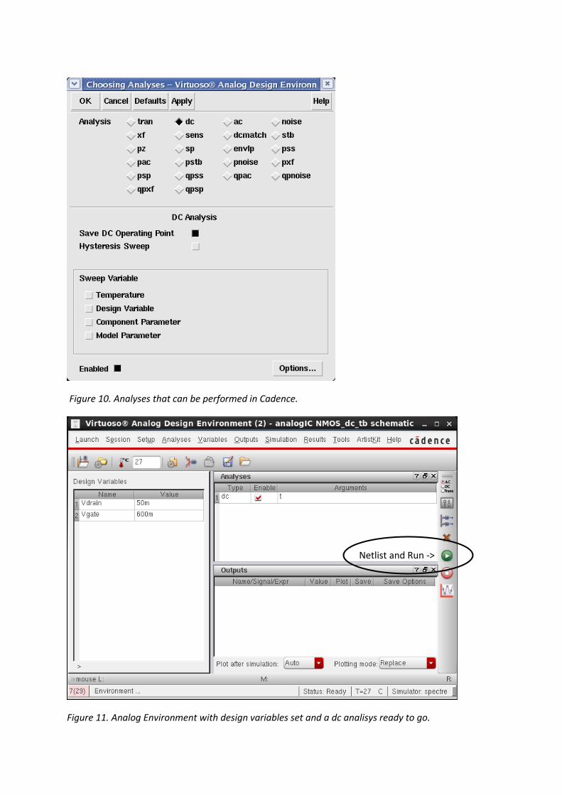
Figure 10. Analyses that can be performed in Cadence.
Figure 11. Analog Environment with design variables set and a dc analisys ready to go.
Netlist and Run ->
Now you are ready to run the simulation. Go to “Simulation -> Netlist and Run” or click on the icon in
the right side menu. When the simulation is done go to the menu “Results” -> “Print” - > “DC
Operating Points” and the click on the NMOS in the schematic window. A new window will appear,
“Results Display Window”, with a list of parameter values from the NMOS-transistor. You can find
the value of e.g. the gate-to-source capacitance cgs, the channel resistance ron in the linear region,
the threshold voltage vth and the drain-to-source current ids. Look through the list and write the
value of the following variables:
cgs = . ron = . vth = . ids = . gm = .
In which region dose this NMOS operates with these bias voltages? .
How do you know that? .
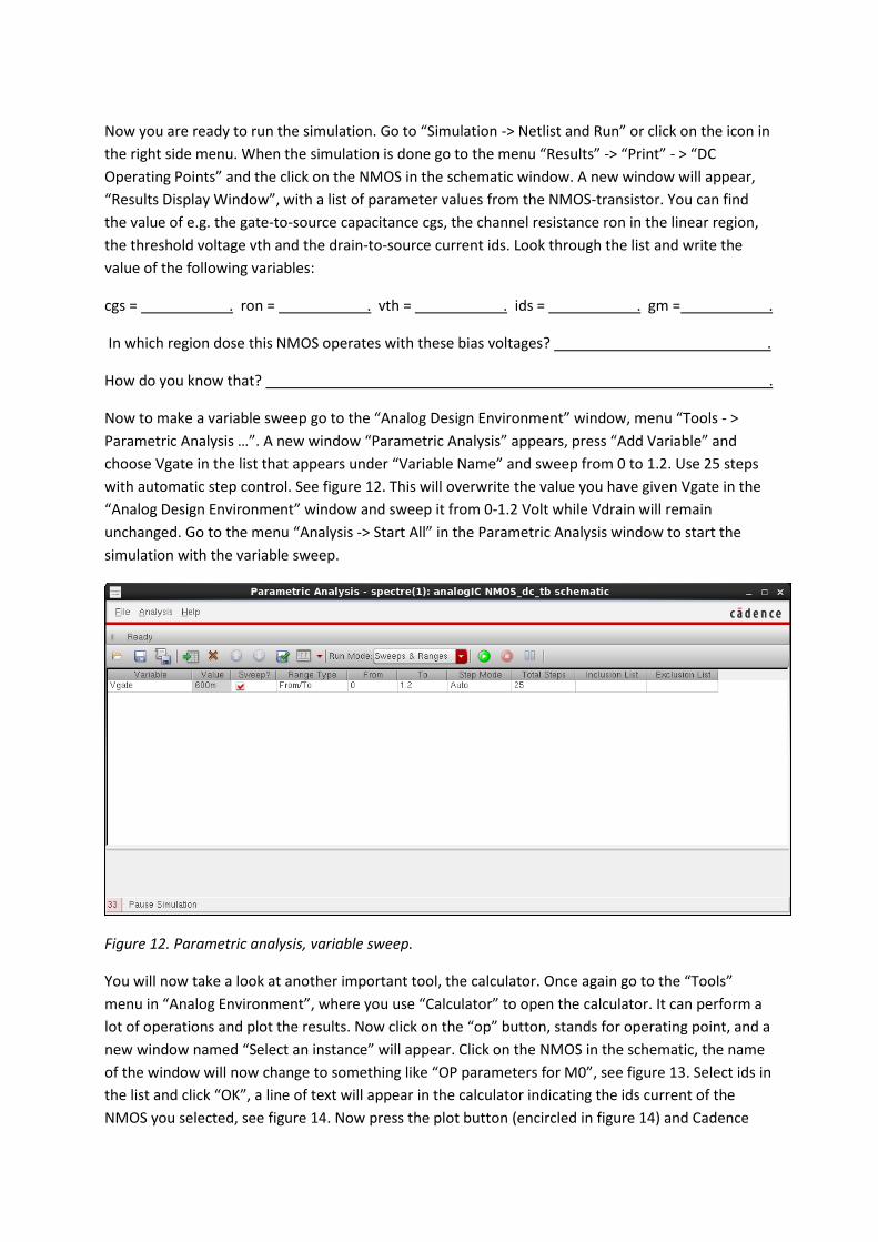
Now to make a variable sweep go to the “Analog Design Environment” window, menu “Tools - >
Parametric Analysis …”. A new window “Parametric Analysis” appears, press “Add Variable” and
choose Vgate in the list that appears under “Variable Name” and sweep from 0 to 1.2. Use 25 steps
with automatic step control. See figure 12. This will overwrite the value you have given Vgate in the
“Analog Design Environment” window and sweep it from 0-1.2 Volt while Vdrain will remain
unchanged. Go to the menu “Analysis -> Start All” in the Parametric Analysis window to start the
simulation with the variable sweep.
Figure 12. Parametric analysis, variable sweep.
You will now take a look at another important tool, the calculator. Once again go to the “Tools”
menu in “Analog Environment”, where you use “Calculator” to open the calculator. It can perform a
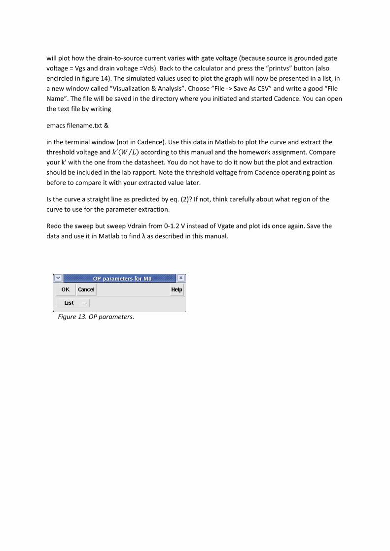
lot of operations and plot the results. Now click on the “op” button, stands for operating point, and a
new window named “Select an instance” will appear. Click on the NMOS in the schematic, the name
of the window will now change to something like “OP parameters for M0”, see figure 13. Select ids in
the list and click “OK”, a line of text will appear in the calculator indicating the ids current of the
NMOS you selected, see figure 14. Now press the plot button (encircled in figure 14) and Cadence
will plot how the drain-to-source current varies with gate voltage (because source is grounded gate
voltage = Vgs and drain voltage =Vds). Back to the calculator and press the “printvs” button (also
encircled in figure 14). The simulated values used to plot the graph will now be presented in a list, in
a new window called “Visualization & Analysis”. Choose ”File -> Save As CSV” and write a good “File
Name”. The file will be saved in the directory where you initiated and started Cadence. You can open
the text file by writing
emacs filename.txt &
in the terminal window (not in Cadence). Use this data in Matlab to plot the curve and extract the
threshold voltage and 𝑘′(𝑊 𝐿⁄ ) according to this manual and the homework assignment. Compare
your k’ with the one from the datasheet. You do not have to do it now but the plot and extraction
should be included in the lab rapport. Note the threshold voltage from Cadence operating point as
before to compare it with your extracted value later.
Is the curve a straight line as predicted by eq. (2)? If not, think carefully about what region of the
curve to use for the parameter extraction.
Redo the sweep but sweep Vdrain from 0-1.2 V instead of Vgate and plot ids once again. Save the
data and use it in Matlab to find λ as described in this manual.
Figure 13. OP parameters.
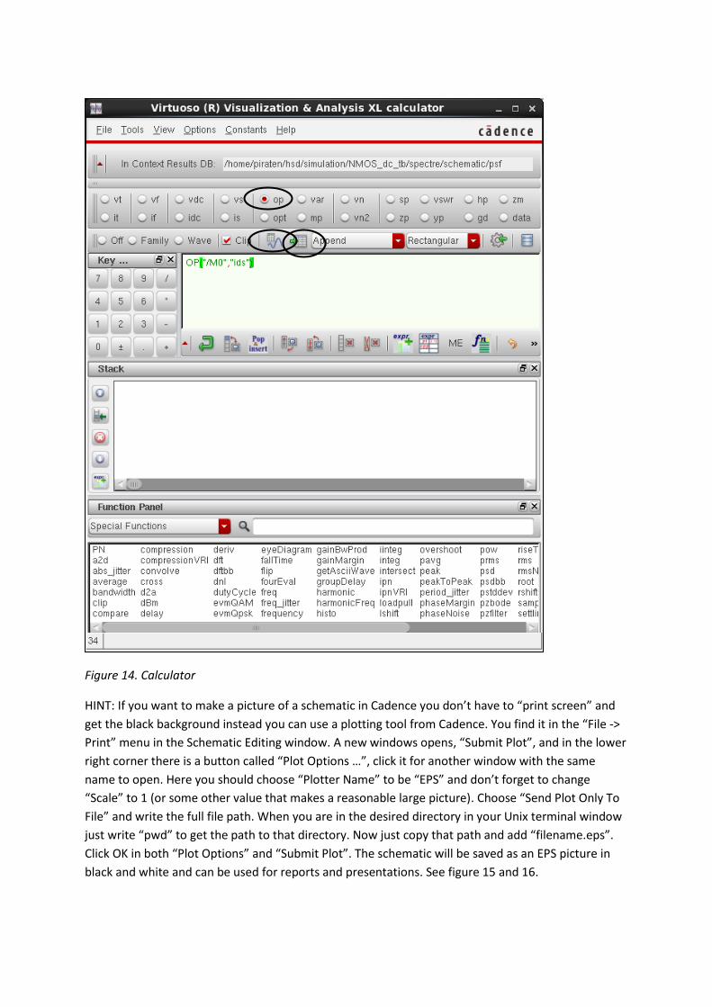
Figure 14. Calculator
HINT: If you want to make a picture of a schematic in Cadence you don’t have to “print screen” and
get the black background instead you can use a plotting tool from Cadence. You find it in the “File ->
Print” menu in the Schematic Editing window. A new windows opens, “Submit Plot”, and in the lower
right corner there is a button called “Plot Options …”, click it for another window with the same
name to open. Here you should choose “Plotter Name” to be “EPS” and don’t forget to change
“Scale” to 1 (or some other value that makes a reasonable large picture). Choose “Send Plot Only To
File” and write the full file path. When you are in the desired directory in your Unix terminal window
just write “pwd” to get the path to that directory. Now just copy that path and add “filename.eps”.
Click OK in both “Plot Options” and “Submit Plot”. The schematic will be saved as an EPS picture in
black and white and can be used for reports and presentations. See figure 15 and 16.
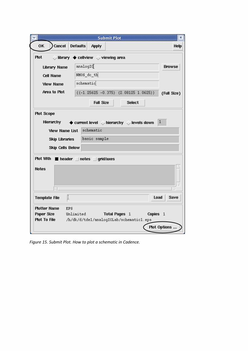
Figure 15. Submit Plot. How to plot a schematic in Cadence.
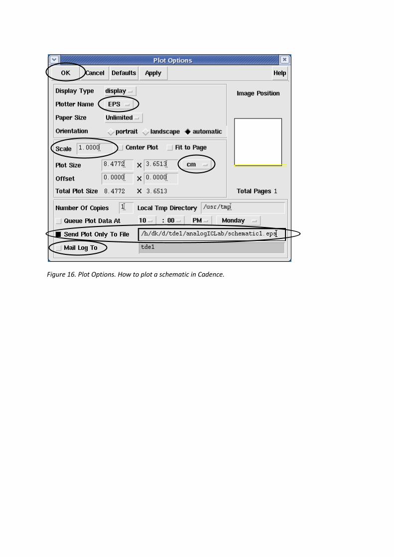
Figure 16. Plot Options. How to plot a schematic in Cadence.
Design and simulation of a PMOS current mirror in Cadence
In this part of the lab a PMOS current mirror schematic will be built and the schematic will be used to
create a symbol view. This is a box representation of the current mirror schematic, which will be used
to simulate the DC output resistance of the current mirror using a testbench. Create a new schematic
cellview with the name “CurrentMirror” in the Library created in previous exercises i.e. analogIC.
Build the current mirror using the PMOS transistor plvtlp. To add the transistors, go to the menu
“Create -> Instance…” (i).
Give the transistors the width and length from homework assignment 5; divide the transistors into 2
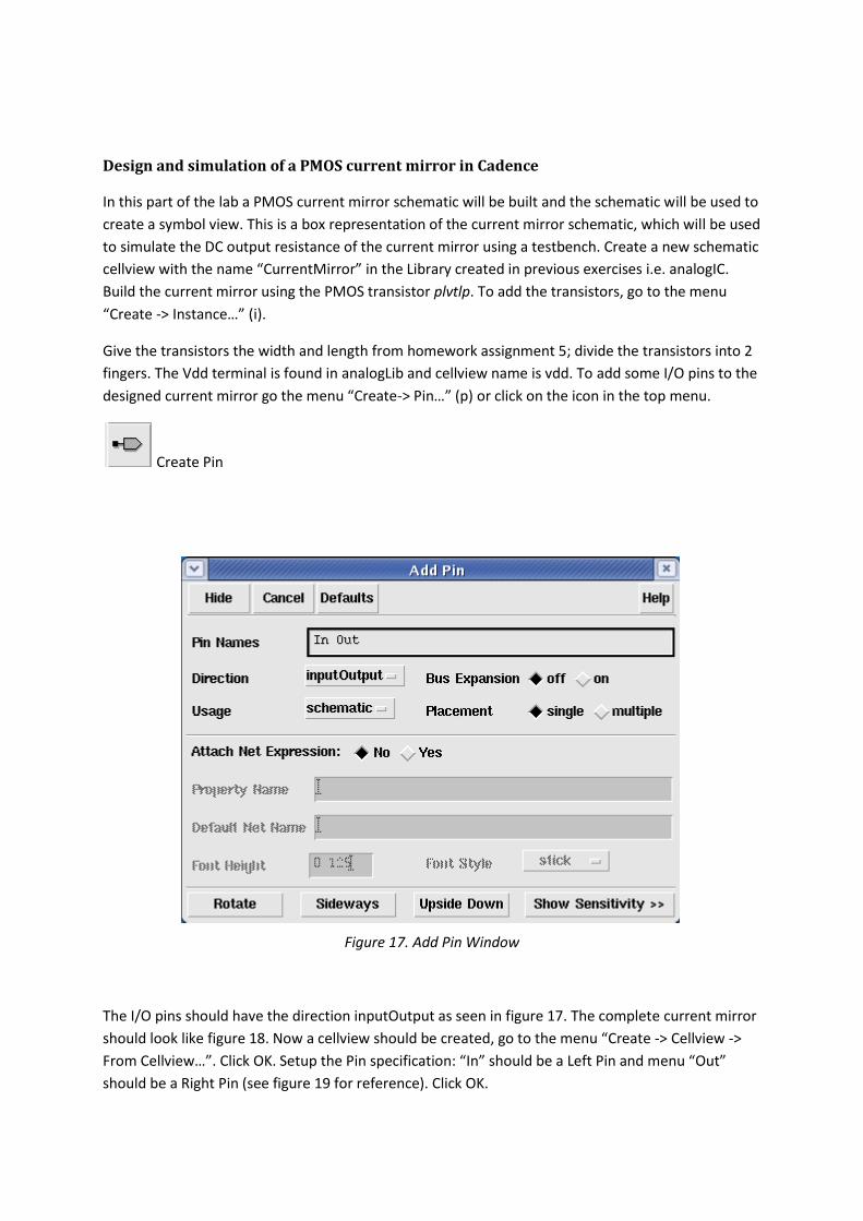
fingers. The Vdd terminal is found in analogLib and cellview name is vdd. To add some I/O pins to the
designed current mirror go the menu “Create-> Pin…” (p) or click on the icon in the top menu.
Create Pin
Figure 17. Add Pin Window
The I/O pins should have the direction inputOutput as seen in figure 17. The complete current mirror
should look like figure 18. Now a cellview should be created, go to the menu “Create -> Cellview ->
From Cellview…”. Click OK. Setup the Pin specification: “In” should be a Left Pin and menu “Out”
should be a Right Pin (see figure 19 for reference). Click OK.
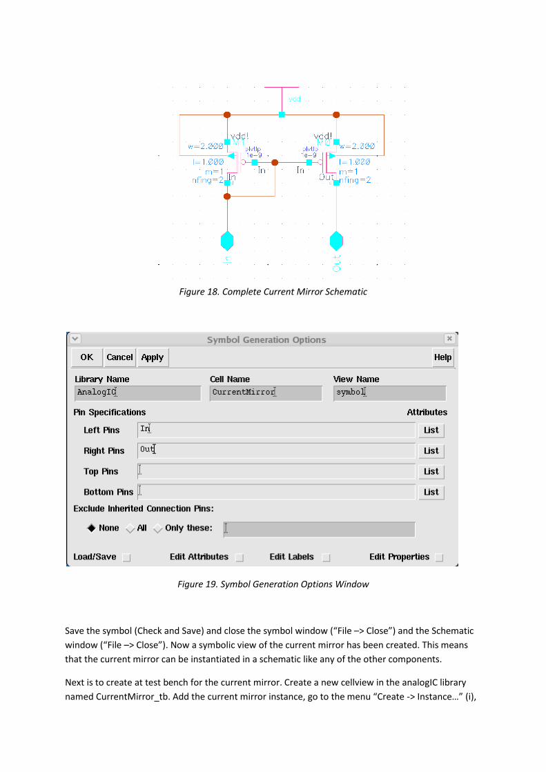
Figure 18. Complete Current Mirror Schematic
Figure 19. Symbol Generation Options Window
Save the symbol (Check and Save) and close the symbol window (“File –> Close”) and the Schematic
window (“File –> Close”). Now a symbolic view of the current mirror has been created. This means
that the current mirror can be instantiated in a schematic like any of the other components.
Next is to create at test bench for the current mirror. Create a new cellview in the analogIC library
named CurrentMirror_tb. Add the current mirror instance, go to the menu “Create -> Instance…” (i),
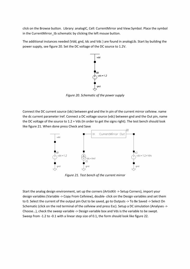
click on the Browse button. Library: analogIC, Cell: CurrentMirror and View:Symbol. Place the symbol
in the CurrentMirror_tb schematic by clicking the left mouse button.
The additional instances needed (Vdd, gnd, Idc and Vdc ) are found in analogLib. Start by building the
power supply, see figure 20. Set the DC voltage of the DC source to 1.2V.
Figure 20. Schematic of the power supply
Connect the DC current source (idc) between gnd and the In pin of the current mirror cellview. name
the dc current parameter Iref. Connect a DC voltage source (vdc) between gnd and the Out pin, name
the DC voltage of the source to 1.2 + Vds (In order to get the signs right). The test bench should look
like figure 21. When done press Check and Save
Figure 21. Test bench of the current mirror
Start the analog design environment, set up the corners (ArtistKit -> Setup Corners), import your
design variables (Variable -> Copy From Cellview), double- click on the Design variables and set them
to 0. Select the current of the output pin Out to be saved, go to Outputs -> To Be Saved -> Select On
Schematic (click on the red terminal of the cellview and press Esc). Setup a DC simulation (Analyses ->
Choose…), check the sweep variable -> Design variable box and Vds is the variable to be swept.
Sweep from -1.2 to -0.1 with a linear step size of 0.1, the form should look like figure 22.
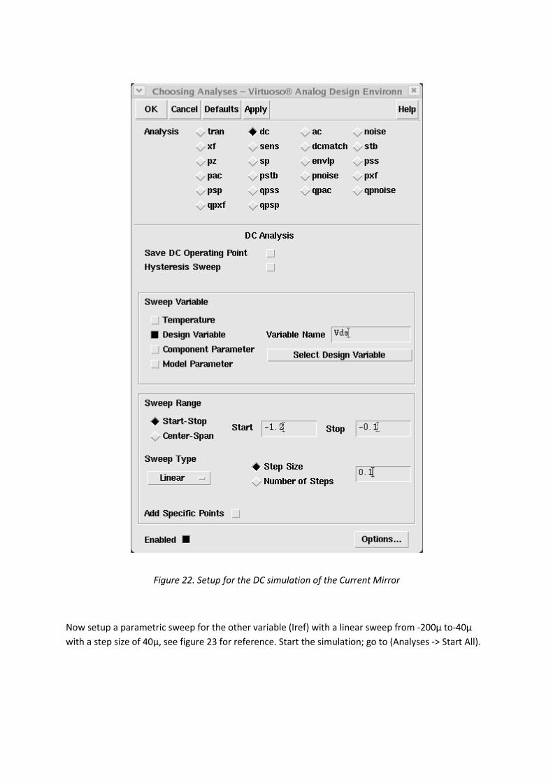
Figure 22. Setup for the DC simulation of the Current Mirror
Now setup a parametric sweep for the other variable (Iref) with a linear sweep from -200µ to-40µ
with a step size of 40µ, see figure 23 for reference. Start the simulation; go to (Analyses -> Start All).
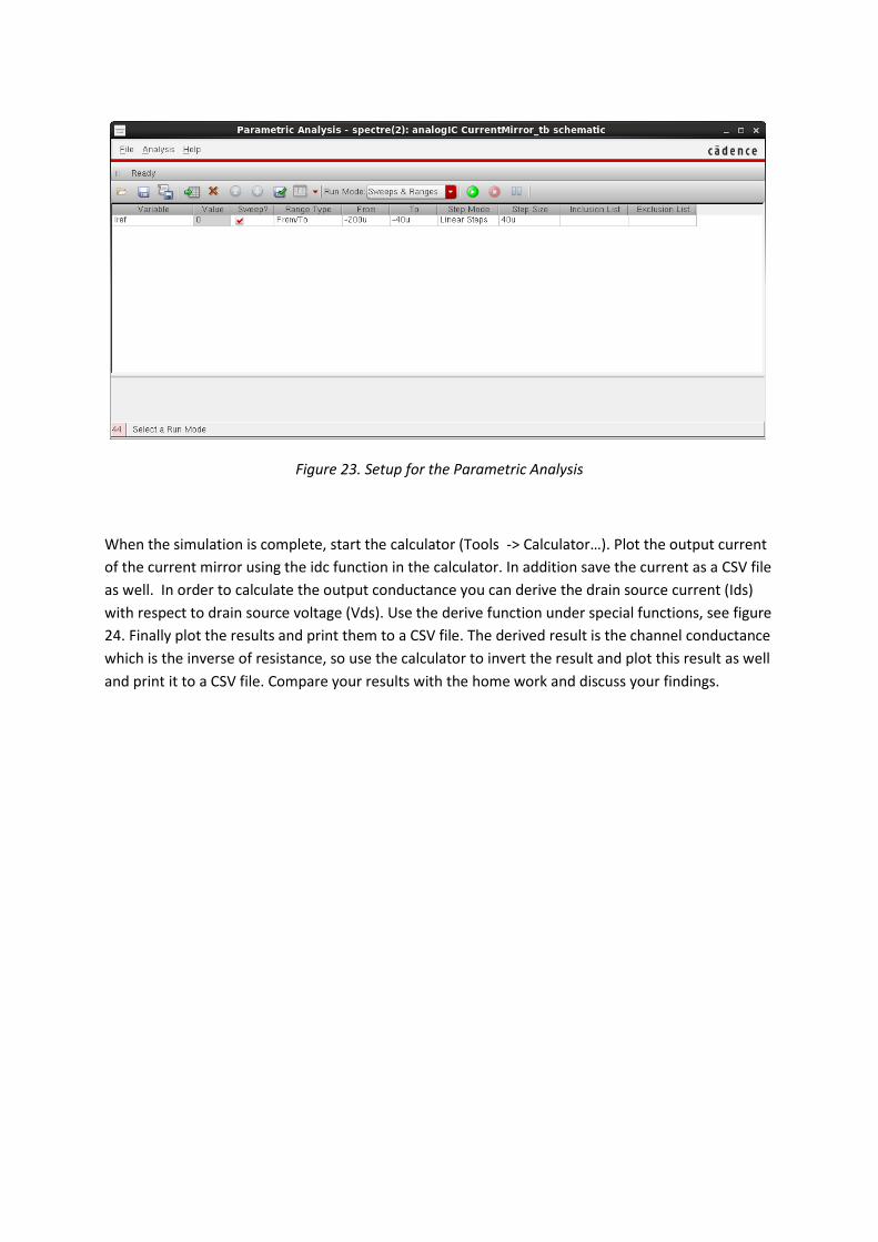
Figure 23. Setup for the Parametric Analysis
When the simulation is complete, start the calculator (Tools -> Calculator…). Plot the output current
of the current mirror using the idc function in the calculator. In addition save the current as a CSV file
as well. In order to calculate the output conductance you can derive the drain source current (Ids)
with respect to drain source voltage (Vds). Use the derive function under special functions, see figure
24. Finally plot the results and print them to a CSV file. The derived result is the channel conductance
which is the inverse of resistance, so use the calculator to invert the result and plot this result as well
and print it to a CSV file. Compare your results with the home work and discuss your findings.
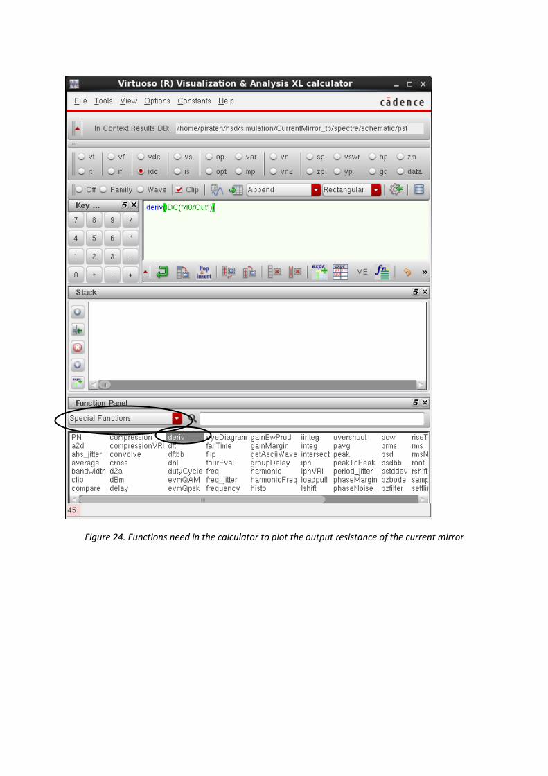
Figure 24. Functions need in the calculator to plot the output resistance of the current mirror
Layout of a PMOS current mirror in Cadence
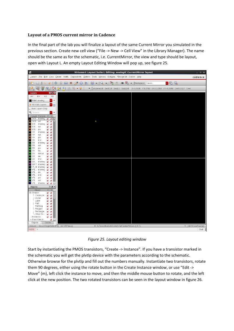
In the final part of the lab you will finalize a layout of the same Current Mirror you simulated in the
previous section. Create new cell view (“File -> New -> Cell View” in the Library Manager). The name
should be the same as for the schematic, i.e. CurrentMirror, the view and type should be layout,
open with Layout L. An empty Layout Editing Window will pop up, see figure 25.
Figure 25. Layout editing window
Start by instantiating the PMOS transistors, “Create -> Instance”. If you have a transistor marked in
the schematic you will get the plvtlp device with the parameters according to the schematic.
Otherwise browse for the plvtlp and fill out the numbers manually. Instantiate two transistors, rotate
them 90 degrees, either using the rotate button in the Create Instance window, or use “Edit ->
Move” (m), left click the instance to move, and then the middle mouse button to rotate, and the left
click at the new position. The two rotated transistors can be seen in the layout window in figure 26.
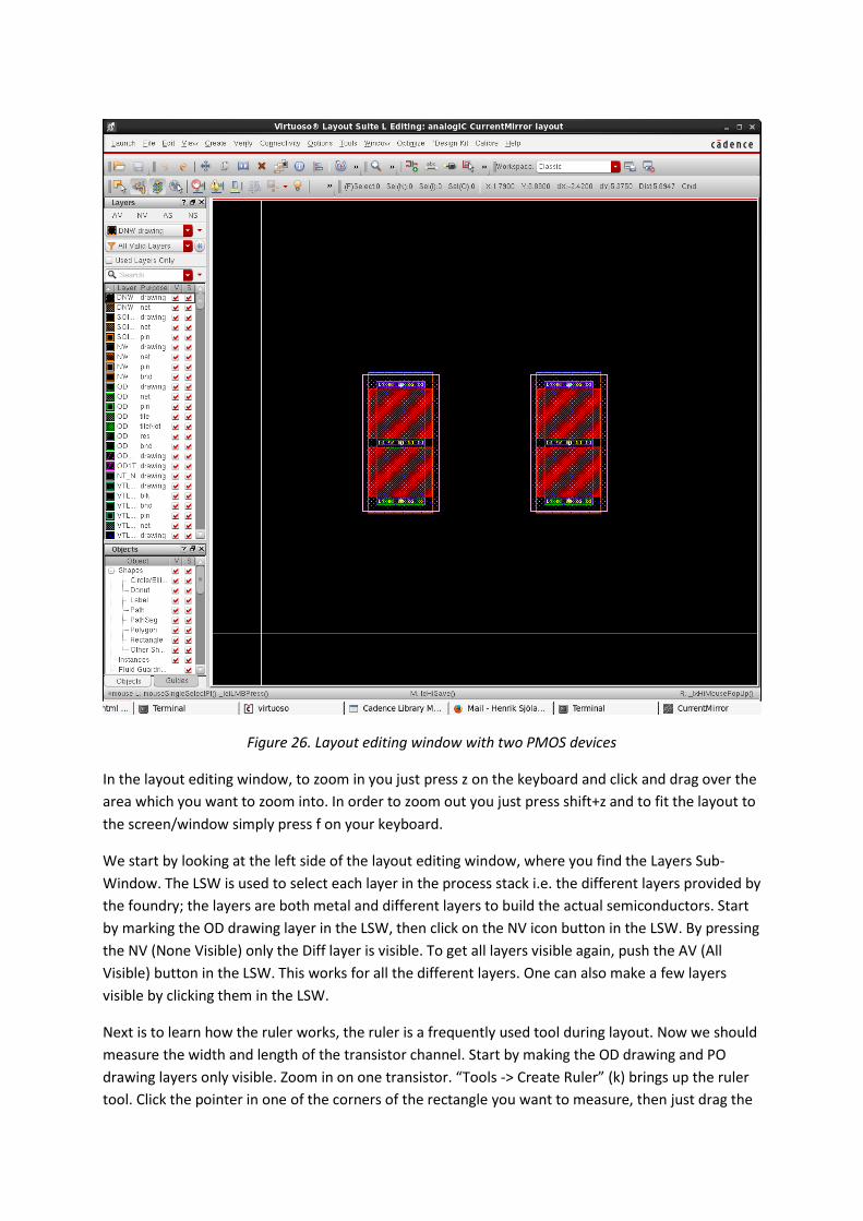
Figure 26. Layout editing window with two PMOS devices
In the layout editing window, to zoom in you just press z on the keyboard and click and drag over the
area which you want to zoom into. In order to zoom out you just press shift+z and to fit the layout to
the screen/window simply press f on your keyboard.
We start by looking at the left side of the layout editing window, where you find the Layers Sub-
Window. The LSW is used to select each layer in the process stack i.e. the different layers provided by
the foundry; the layers are both metal and different layers to build the actual semiconductors. Start
by marking the OD drawing layer in the LSW, then click on the NV icon button in the LSW. By pressing
the NV (None Visible) only the Diff layer is visible. To get all layers visible again, push the AV (All
Visible) button in the LSW. This works for all the different layers. One can also make a few layers
visible by clicking them in the LSW.
Next is to learn how the ruler works, the ruler is a frequently used tool during layout. Now we should
measure the width and length of the transistor channel. Start by making the OD drawing and PO
drawing layers only visible. Zoom in on one transistor. “Tools -> Create Ruler” (k) brings up the ruler
tool. Click the pointer in one of the corners of the rectangle you want to measure, then just drag the
pointer to the corner on the opposite side of the rectangle and click. Where do you measure the
transistor channel length, and the width? Use the ruler to measure both. Finally remove the rulers by
“Tools -> Clear All Rulers” (shift+k).
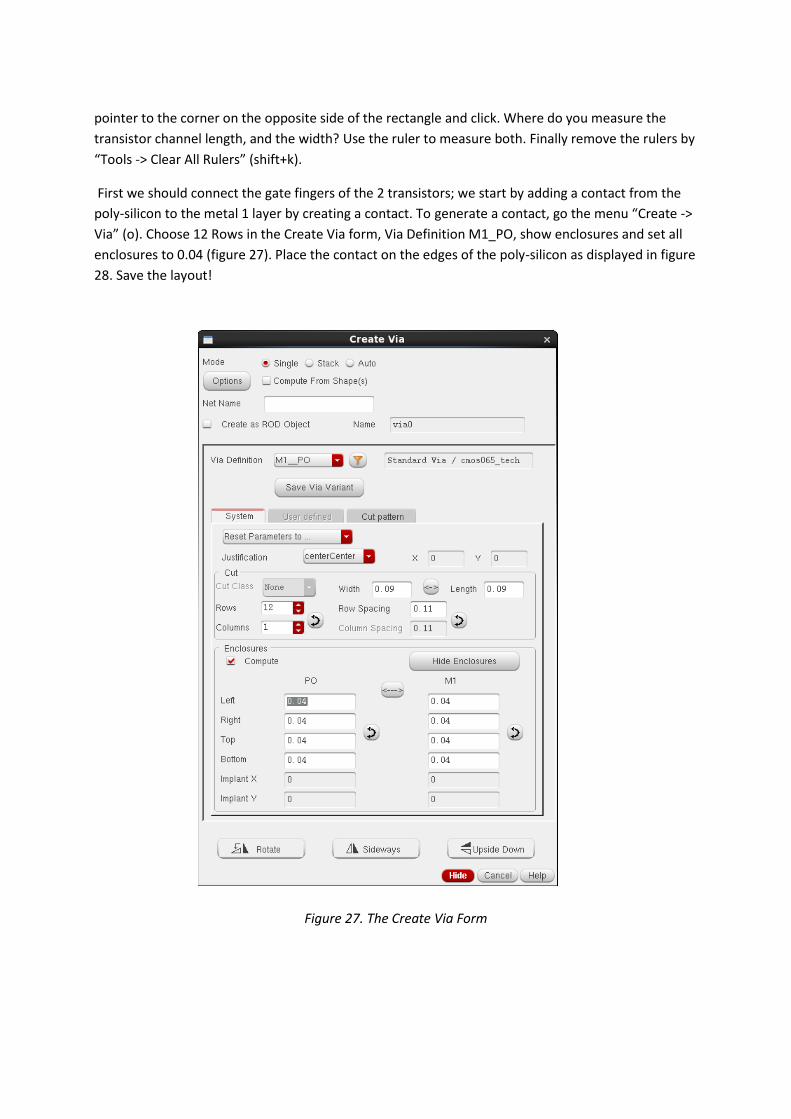
First we should connect the gate fingers of the 2 transistors; we start by adding a contact from the
poly-silicon to the metal 1 layer by creating a contact. To generate a contact, go the menu “Create ->
Via” (o). Choose 12 Rows in the Create Via form, Via Definition M1_PO, show enclosures and set all
enclosures to 0.04 (figure 27). Place the contact on the edges of the poly-silicon as displayed in figure
28. Save the layout!
Figure 27. The Create Via Form
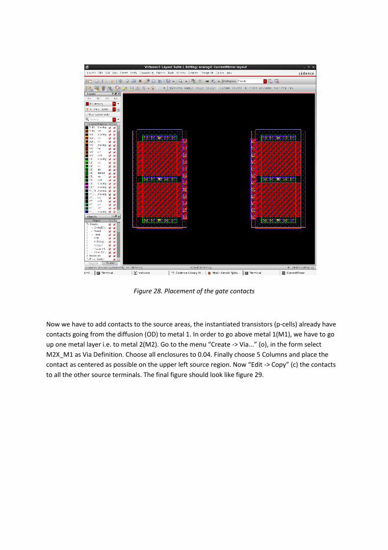
Figure 28. Placement of the gate contacts
Now we have to add contacts to the source areas, the instantiated transistors (p-cells) already have
contacts going from the diffusion (OD) to metal 1. In order to go above metal 1(M1), we have to go
up one metal layer i.e. to metal 2(M2). Go to the menu “Create -> Via...” (o), in the form select
M2X_M1 as Via Definition. Choose all enclosures to 0.04. Finally choose 5 Columns and place the
contact as centered as possible on the upper left source region. Now “Edit -> Copy” (c) the contacts
to all the other source terminals. The final figure should look like figure 29.
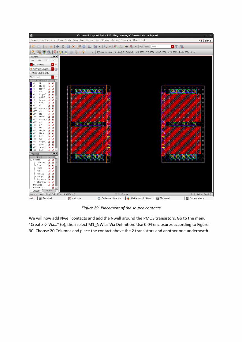
Figure 29. Placement of the source contacts
We will now add Nwell contacts and add the Nwell around the PMOS transistors. Go to the menu
“Create -> Via…” (o), then select M1_NW as Via Definition. Use 0.04 enclosures according to Figure
30. Choose 20 Columns and place the contact above the 2 transistors and another one underneath.
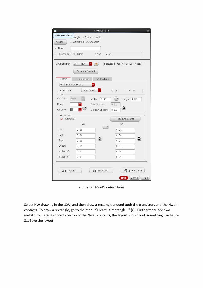
Figure 30. Nwell contact form
Select NW drawing in the LSW, and then draw a rectangle around both the transistors and the Nwell
contacts. To draw a rectangle, go to the menu “Create -> rectangle…” (r). Furthermore add two
metal 1 to metal 2 contacts on top of the Nwell contacts, the layout should look something like figure
31. Save the layout!
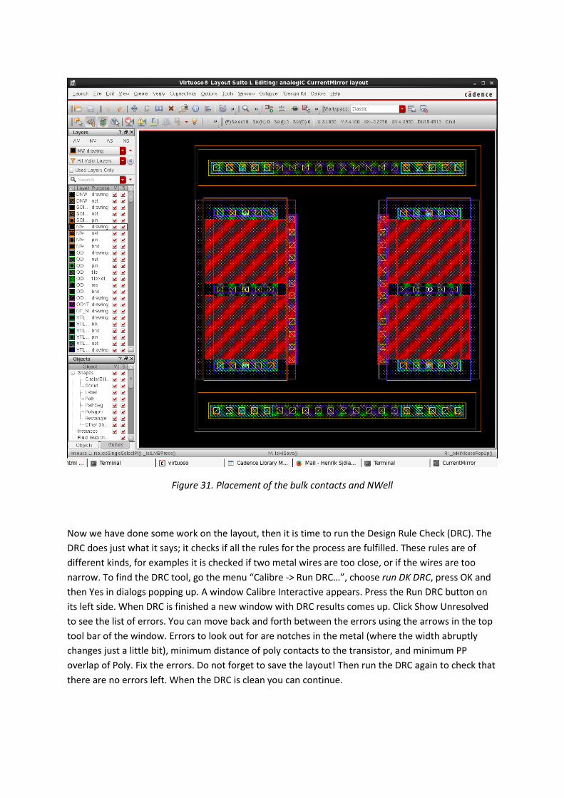
Figure 31. Placement of the bulk contacts and NWell
Now we have done some work on the layout, then it is time to run the Design Rule Check (DRC). The
DRC does just what it says; it checks if all the rules for the process are fulfilled. These rules are of
different kinds, for examples it is checked if two metal wires are too close, or if the wires are too
narrow. To find the DRC tool, go the menu “Calibre -> Run DRC…”, choose run DK DRC, press OK and
then Yes in dialogs popping up. A window Calibre Interactive appears. Press the Run DRC button on
its left side. When DRC is finished a new window with DRC results comes up. Click Show Unresolved
to see the list of errors. You can move back and forth between the errors using the arrows in the top
tool bar of the window. Errors to look out for are notches in the metal (where the width abruptly
changes just a little bit), minimum distance of poly contacts to the transistor, and minimum PP
overlap of Poly. Fix the errors. Do not forget to save the layout! Then run the DRC again to check that
there are no errors left. When the DRC is clean you can continue.
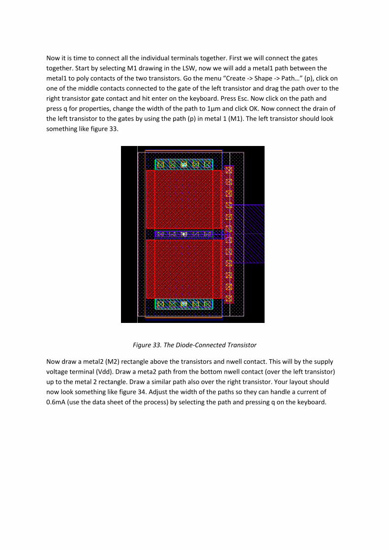
Now it is time to connect all the individual terminals together. First we will connect the gates
together. Start by selecting M1 drawing in the LSW, now we will add a metal1 path between the
metal1 to poly contacts of the two transistors. Go the menu “Create -> Shape -> Path…” (p), click on
one of the middle contacts connected to the gate of the left transistor and drag the path over to the
right transistor gate contact and hit enter on the keyboard. Press Esc. Now click on the path and
press q for properties, change the width of the path to 1µm and click OK. Now connect the drain of
the left transistor to the gates by using the path (p) in metal 1 (M1). The left transistor should look
something like figure 33.
Figure 33. The Diode-Connected Transistor
Now draw a metal2 (M2) rectangle above the transistors and nwell contact. This will by the supply
voltage terminal (Vdd). Draw a meta2 path from the bottom nwell contact (over the left transistor)
up to the metal 2 rectangle. Draw a similar path also over the right transistor. Your layout should
now look something like figure 34. Adjust the width of the paths so they can handle a current of
0.6mA (use the data sheet of the process) by selecting the path and pressing q on the keyboard.
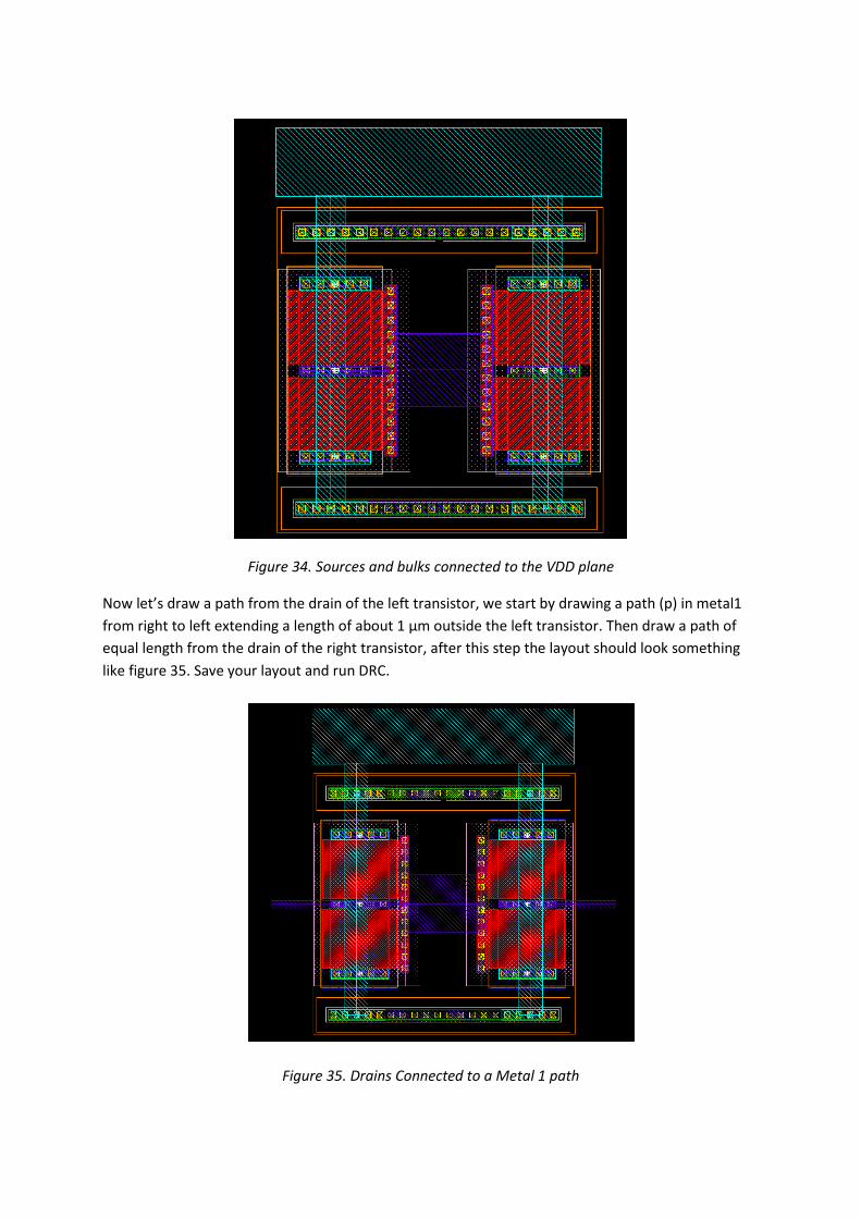
Figure 34. Sources and bulks connected to the VDD plane
Now let’s draw a path from the drain of the left transistor, we start by drawing a path (p) in metal1
from right to left extending a length of about 1 µm outside the left transistor. Then draw a path of
equal length from the drain of the right transistor, after this step the layout should look something
like figure 35. Save your layout and run DRC.
Figure 35. Drains Connected to a Metal 1 path
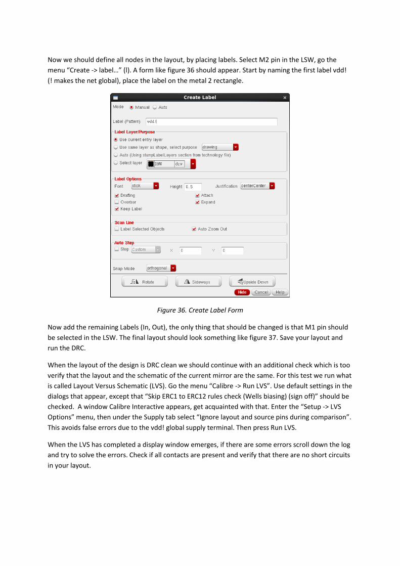
Now we should define all nodes in the layout, by placing labels. Select M2 pin in the LSW, go the
menu “Create -> label…” (l). A form like figure 36 should appear. Start by naming the first label vdd!
(! makes the net global), place the label on the metal 2 rectangle.
Figure 36. Create Label Form
Now add the remaining Labels (In, Out), the only thing that should be changed is that M1 pin should
be selected in the LSW. The final layout should look something like figure 37. Save your layout and
run the DRC.
When the layout of the design is DRC clean we should continue with an additional check which is too
verify that the layout and the schematic of the current mirror are the same. For this test we run what
is called Layout Versus Schematic (LVS). Go the menu “Calibre -> Run LVS”. Use default settings in the
dialogs that appear, except that “Skip ERC1 to ERC12 rules check (Wells biasing) (sign off)” should be
checked. A window Calibre Interactive appears, get acquainted with that. Enter the “Setup -> LVS
Options” menu, then under the Supply tab select “Ignore layout and source pins during comparison”.
This avoids false errors due to the vdd! global supply terminal. Then press Run LVS.
When the LVS has completed a display window emerges, if there are some errors scroll down the log
and try to solve the errors. Check if all contacts are present and verify that there are no short circuits
in your layout.
Figure 37. Final Layout
Laboratory Report
Compose a report containing the difference of calculated and simulated values. The report should
also answer the questions in the homework section, and explain the results from the laboratory.
Include plots of the simulated figures.


![[ASM] Lab1](https://static.fdocuments.in/doc/165x107/588121881a28abb9388b706b/asm-lab1.jpg)