Analog IC Design 12
52
Department of Electrical Engineering C ha pt e r 1 2 C ha pt e r 1 2 Switched Switched - - C a pa citor C i r cui t s C a pa ci t or C i r cui t s
-
Upload
alexlhhcas -
Category
Documents
-
view
232 -
download
0
Transcript of Analog IC Design 12

8/12/2019 Analog IC Design 12
http://slidepdf.com/reader/full/analog-ic-design-12 1/52
Department of Electrical Engineering
Chapter 12 Chapter 12 Switched Switched - - Capacitor Circuits Capacitor Circuits

8/12/2019 Analog IC Design 12
http://slidepdf.com/reader/full/analog-ic-design-12 2/52
2
Introduction Introduction “Discrete-Time” or “Sampled-Data” Systems
In many situations, we may sense the input only at periodic instants of time, ignoring itsvalue at other times
The circuit processes each “sample”, producing a valid output at the end of each
period
In this lecture, we study a common class of discrete-time systems called “switched-
capacitor (SC) circuits”
Our objective is to provide the foundation for more advanced topics such as filters,
comparators, ADCs, and DACs
Most of our study deals with switched-capacitor amplifiers but the concepts can be applied
to other discrete-time circuits as well

8/12/2019 Analog IC Design 12
http://slidepdf.com/reader/full/analog-ic-design-12 3/52
3
General Considerations General Considerations Continuous-Time Feedback Amplifier
By the equivalent circuit, we have
Thus
Compared to the case where Rout
= 0
the close-loop gain suffers from inaccuracies
in both the numerator and the denominator
The input resistance of the amplifier, approximatelyequal to R1, loads the preceding stage while introducing
thermal noise
out inout
out ininout
v V R R
V V RV
R R
V V R A =
+
−−⎟⎟
⎠
⎞⎜⎜⎝
⎛ +
+
−−
21211
1
2
1
2
1
2
1 R
R A
R
R
R
R A
R
R
V
V
vout
out v
in
out
+++
−⋅−=
Equivalent circuit

8/12/2019 Analog IC Design 12
http://slidepdf.com/reader/full/analog-ic-design-12 4/52
4
General Considerations General Considerations Continuous-Time Feedback Amplifier Using Capacitors
Such an arrangement of the circuit is indeed practical
if the circuit senses only high-frequency signals
A large feedback RF is used to bias node X
The step response contains a step change due to theinitial amplification by the circuit consisting of C1, C2,
and the op amp, followed by a “tail” resulting from the
loss of charge on C2 through RF
The circuit is not suited to amplify wideband signals
because it exhibits a high-pass transfer function
indicating that Vout/Vin ≈ −C1/C2 only if ω >> (RF C2)−1
The difficulty can be remedied by increasing RF C2
But in many applications the required values of the
two components become prohibitively large
1)(
2
1
+−≈
sC R
sC Rs
V
V
F
F
in
out
Using RF to define bias point
Step response

8/12/2019 Analog IC Design 12
http://slidepdf.com/reader/full/analog-ic-design-12 5/52
5
General Considerations General Considerations Switched-Capacitor Amplifier
Charge conservation equations Q=CV
Sampling mode Transfer of charge from C1 to C2 Amplification mode

8/12/2019 Analog IC Design 12
http://slidepdf.com/reader/full/analog-ic-design-12 6/52
6
General Considerations General Considerations General View of Switched-Capacitor Amplifier
Discrete-time operations require switches to perform sampling as well as a high input
impedance to sense the stored quantities with no corruption
Thus, the existence of simple switches and a high input impedance has made CMOS
technology the dominant choice for sampled-data applications
In the simplest switch-capacitor amplifiers, the operation takes in two phases
sampling and amplification

8/12/2019 Analog IC Design 12
http://slidepdf.com/reader/full/analog-ic-design-12 7/52
7
Sampling Switches Sampling Switches MOSFET as Switches
Simple sampling circuit – the switch by a MOS device
Response of different input levels and initial conditions
( )( )TH DDoxn
onV V LW C
R−
=/
1
μ ( )( )TH in DDoxn
onV V V LW C
R−−
=/
1
μ

8/12/2019 Analog IC Design 12
http://slidepdf.com/reader/full/analog-ic-design-12 8/52
8
Sampling Switches Sampling Switches Track and Hold Capabilities of a Sampling Circuit

8/12/2019 Analog IC Design 12
http://slidepdf.com/reader/full/analog-ic-design-12 9/52
9
Sampling Switches Sampling Switches Maximum Output Level in an NMOS Sampler
Since the gate and drain of M1 are at the same potential, the transistor is saturated
Thus
implies that as t → infinity, Vout → VDD − VTH
For Vout ≈ Vin, the transistor must operate in deep triode region and the upper bound of
Vin equals VDD − VTH. In practice, Vin must be quite lower than this value.
( )2
12
1TH out DDoxn D
out H V V V
L
W C I
dt
dV C −−== μ
t
H
oxn
V
TH out DD
t L
W
C
C
V V V
out
002
11μ =
−−( ) dt
L
W
C
C
V V V
dV
H
oxn
TH out DD
out μ 2
12 =
−−
TH DD H
oxn
TH DDout
V V t
LW
C C
V V V
−+
−−=1
21
1
μ
(neglecting channel-length modulation)

8/12/2019 Analog IC Design 12
http://slidepdf.com/reader/full/analog-ic-design-12 10/52

8/12/2019 Analog IC Design 12
http://slidepdf.com/reader/full/analog-ic-design-12 11/52
11
Sampling Switches Sampling Switches Definition of Speed in a Sampling Circuit
ΔV/Vin0 = 0.1%
note that after t = tS, we can consider the source and drain voltages be approximately
equal
The sampling speed is given by two factors
the on-resistance of the switch
the value of the sampling capacitor

8/12/2019 Analog IC Design 12
http://slidepdf.com/reader/full/analog-ic-design-12 12/52
12
Sampling Switches Sampling Switches On-Resistance of MOS Devices
On-resistance of NMOS/PMOS devices as a function of input voltage
If we restrict the variation of Ron to a range of 4 to 1, then the maximum input level is given
by
⇒
This value falls around VDD/2, translating to severe swing limitations
Note that the device threshold voltage directly limits the voltage swings
( ) ( )TH DDoxnTH in DDoxn
V V L
W C V V V
L
W C −
=−− μ μ
41
max,
( )TH DDin V V V −=
4
3max,

8/12/2019 Analog IC Design 12
http://slidepdf.com/reader/full/analog-ic-design-12 13/52
13
Sampling Switches Sampling Switches Complementary Switch
Equivalent resistance
If μ nCox(W/L)N = μ PCox(W/L)P
then Ron,eq is independent of the input level
( ) ( )
( ) THPP
ox pinP
ox p N
oxnTHN DD N
oxn
THPin
P
ox pTHN in DD
N
oxn
Pon N oneqon
V L
W C V
L
W C
L
W C V V
L
W C
V V L
W C V V V
L
W C
R R R
⎟ ⎠
⎞
⎜⎝
⎛ −⎥⎦
⎤
⎢⎣
⎡
⎟ ⎠
⎞
⎜⎝
⎛ −⎟ ⎠
⎞
⎜⎝
⎛ −−⎟ ⎠
⎞
⎜⎝
⎛ =
−⎟ ⎠ ⎞
⎜⎝ ⎛ −−⎟
⎠ ⎞
⎜⎝ ⎛ ==
μ μ μ μ
μ μ
1
11,,,

8/12/2019 Analog IC Design 12
http://slidepdf.com/reader/full/analog-ic-design-12 14/52
14
Sampling Switches Sampling Switches Complementary Switch
Distortion generated if complementary switches do not turn off simultaneously
Simple circuit generating complementary clocks

8/12/2019 Analog IC Design 12
http://slidepdf.com/reader/full/analog-ic-design-12 15/52
15
Sampling Switches Sampling Switches Channel Charge Injection
Charge injection when a switch turns off
Assuming Vin ≈ Vout, the total charge in the inversion layer is
Qch = WLCox(VDD − Vin − VTH)
When the switch turns off , Qch exits through the source anddrain terminals, a phenomenon called “channel charge injection”
Effect of charge injection
For example, if half of Qch is injected onto CH the resulting error equals
The error is directly proportional to WLCox
and inversely proportional to CH
( )
H
TH in DDox
C
V V V WLC V
2
−−=Δ

8/12/2019 Analog IC Design 12
http://slidepdf.com/reader/full/analog-ic-design-12 16/52

8/12/2019 Analog IC Design 12
http://slidepdf.com/reader/full/analog-ic-design-12 17/52
17
Sampling Switches Sampling Switches Body Effect
Since and VSB ≈ Vin, we have
It follows that the nonlinear dependence of VTH upon Vin introduces nonlinearity in the
input/output characteristic
In summary, charge injection contributes three types of errors in MOS sampling circuits
gain error
dc offsets
Nonlinearity
In many applications, the first two can be tolerated or corrected whereas the last cannot
) BSB BTH TH V V V φ φ γ 220 −++=
( )
( ) BTH DD
H
oxin B
H
ox
H
oxin
Bin BTH in DD
H
oxinout
V V C
WLC V C
WLC C
WLC V
V V V V C
WLC V V
φ γ φ γ
φ γ φ γ
221
22
0
0
+−−++⎟⎟ ⎠
⎞⎜⎜⎝
⎛ +=
++−−−−=

8/12/2019 Analog IC Design 12
http://slidepdf.com/reader/full/analog-ic-design-12 18/52
18
Sampling Switches Sampling Switches Channel Charge Injection
It is instructive to consider the speed-precision trade-off resulting from charge injection
Representing the speed by a simple time constant τ and the precision by the error ΔV due
to charge injection, we define a figure of merit as F = (τ ΔV)−1
The trade-off is independent of the switch width and the sampling capacitor
2LF nμ =
( )( )
( )THinDDH
ox
HTHinDDoxn
Hon
VVVC
WLCV
CVVVLWC
CR
−−=Δ
−−==
/μ τ
1
S li S it h

8/12/2019 Analog IC Design 12
http://slidepdf.com/reader/full/analog-ic-design-12 19/52
19
Sampling Switches Sampling Switches Clock Feedthrough
Assuming the overlap capacitance is constant, we express the error as
where Cov is the overlap capacitance per unit width
The error ΔV is independent of the input level
manifesting itself as a constant offset in the input/output characteristic
As with charge injection, clock feedthrough leads to a trade-off between speed andprecision as well
H ov
ovCK
C WC
WC V V
+=Δ
S li S i hS li S it h

8/12/2019 Analog IC Design 12
http://slidepdf.com/reader/full/analog-ic-design-12 20/52
20
Sampling Switches Sampling Switches kT/C Noise
The on-resistance of the switch introduces thermal noise at the outputwhen the switch turns off , this noise is stored on the capacitor along with the instantaneous
value of the input voltage
The rms voltage of the sampled noise is approximately equal to
The problem of kT/C noise limits the performance in many high-precision applications
In order to achieve a low noise, the sampling capacitor must be sufficiently large, thus
loading other circuits and degrading the speed
C kT /
S li S it hS li S it h

8/12/2019 Analog IC Design 12
http://slidepdf.com/reader/full/analog-ic-design-12 21/52
21
Sampling Switches Sampling Switches Charge Injection Cancellation
Addition of dummy device to reduce charge injection and clock feedthrough A “dummy” switch, M2, driven by is added to the circuit
such that after M1 turns off and M2 turns on, the channel charge deposited by the former on C H
is absorbed by the latter to create a channel
Suppose half of the channel charge of M1 is injected onto CH, i.e.,
Since Δq2 = W2L2Cox(VCK − Vin − VTH2), if we choose
W2 = 0.5W1 and L2 = L1, then Δq2 = Δq1
Unfortunately, the assumption of equal splitting of charge
between source and drain is generally invalid, making this
approach less attractive
CK
( )111
12
TH inCK ox V V V
C LW q −−=Δ
S li S it hS li S it h

8/12/2019 Analog IC Design 12
http://slidepdf.com/reader/full/analog-ic-design-12 22/52
22
Sampling Switches Sampling Switches Clock Feedthrough Suppression by Dummy Switch
With the choice W2 = 0.5W1 and L2 = L1, the effect of clock feedthrough is suppressedThe total charge in Vout is zero because
02
2
221
2
21
1 =++
+++
−ov H ov
ov
CK
ov H ov
ov
CK C W C C W
C W V
C W C C W
C W V
S li S it hS li S it h

8/12/2019 Analog IC Design 12
http://slidepdf.com/reader/full/analog-ic-design-12 23/52
23
Sampling Switches Sampling Switches Use of Complementary Switches to Reduce Charge Injection
The approach to lowering the effect of charge injection incorporates both PMOS andNMOS devices
such that the opposite charge packets injected by the two cancel each other
For Δq1 to cancel Δq2, we must have W1L1Cox(VCK − Vin − VTHN) = W2L2Cox(Vin − |VTHP|)Thus, the cancellation occurs for only one input level
Even for clock feedthrough, the circuit does not provide complete cancellation
because the gate-drain overlap capacitance of NFETs is not equal to that of PFETs
S li S it hSampling Switches
8/12/2019 Analog IC Design 12
http://slidepdf.com/reader/full/analog-ic-design-12 24/52
24
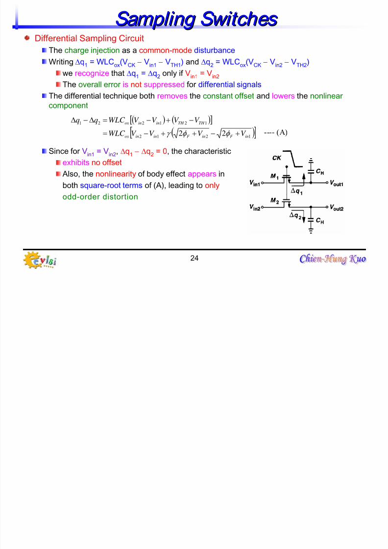
Sampling Switches Sampling Switches Differential Sampling Circuit
The charge injection as a common-mode disturbanceWriting Δq1 = WLCox(VCK − Vin1 − VTH1) and Δq2 = WLCox(VCK − Vin2 − VTH2)
we recognize that Δq1 = Δq2 only if Vin1 = Vin2
The overall error is not suppressed for differential signals
The differential technique both removes the constant offset and lowers the nonlinearcomponent
Since for Vin1 = Vin2, Δq1 − Δq2 = 0, the characteristic
exhibits no offset
Also, the nonlinearity of body effect appears in
both square-root terms of (A), leading to only
odd-order distortion
( ) ( )[ ]
( )[ ]1212
121221
22inF inF ininox
TH TH ininox
V V V V WLC
V V V V WLC qq
+−++−=
−+−=Δ−Δ
φ φ γ ---- (A)
S itchedSwitched Capacitor AmplifierCapacitor Amplifier

8/12/2019 Analog IC Design 12
http://slidepdf.com/reader/full/analog-ic-design-12 25/52
25
Switched Switched - - Capacitor Amplifier Capacitor Amplifier Simple Capacitor Structure
The “top plate” is realized by a polysilicon layer and the “bottom plate” by a heavily doped
n+ region
The dielectric is the thin oxide layer used in MOS device
An important concern in using this structure is the parasitic capacitance between each
plate and the substrateIn particular, the bottom plate suffers from substantial junction capacitance to the
underlying p region – typically about 10 ~ 20% of the oxide capacitance
Parasitic capacitance to the substrate
SwitchedSwitched Capacitor AmplifierCapacitor Amplifier

8/12/2019 Analog IC Design 12
http://slidepdf.com/reader/full/analog-ic-design-12 26/52
26
Switched Switched - - Capacitor Amplifier Capacitor Amplifier Unity-Gain Buffer
Unity-Gain Sampler
for continuous-time application for discrete-time application
The input-independent charge injected by S1 onto CH limit the accuracy
In sampling mode
In amplification mode
S2 turns off slightly
before S1 does
independent of the input level
because node X is a virtual ground
Δq2 = WLCox(VCK − VTH − VX)
Although body effect makes VTH afunction of VX, Δq2 is relatively
constant (offset) because VX is quite
independent of Vin
SwitchedSwitched Capacitor AmplifierCapacitor Amplifier

8/12/2019 Analog IC Design 12
http://slidepdf.com/reader/full/analog-ic-design-12 27/52
27
Switched Switched - - Capacitor Amplifier Capacitor Amplifier Operation of Unit-Gain Sampler in Slow Motion
The effect of the charge injected by S1
Assuming the total charge at node X is zero
C XV X
− (V out
− V X
)C H
= 0, and V X
= −V out
/ Av1
⇒ −(C X
+ C H
)V out
/ Av1 − V
out C H
= 0, i.e., V out
= 0
This result is independent of Δq1, capacitor
values, or the gain of the op amp
thereby revealing that the charge injection by S1 introduces no error if S2 turns off first
finite op amp input capacitance
Transition of circuit to amplification mode
SwitchedSwitched Capacitor AmplifierCapacitor Amplifier

8/12/2019 Analog IC Design 12
http://slidepdf.com/reader/full/analog-ic-design-12 28/52
28
Switched Switched - - Capacitor Amplifier Capacitor Amplifier Operation of Unit-Gain Sampler in Slow Motion
The effect of the charge injected by S3
In order to turn on, S3 must establish an inversion layer at its oxide interface
However, after the feedback circuit has settled, the charge on CH equal V0CH,
unaffected by S3. The channel charge of this switch is therefore entirely supplied by
the op amp, introducing no error
Generation of proper clock edges for unity-gain sampler
With proper timing, the charge injected by S1 and S3 is unimportant
The channel charge of S2 results in a constant offset voltage
We must ensure S1 turns off after S2 does
SwitchedSwitched Capacitor AmplifierCapacitor Amplifier

8/12/2019 Analog IC Design 12
http://slidepdf.com/reader/full/analog-ic-design-12 29/52
29
Switched Switched - - Capacitor Amplifier Capacitor Amplifier Differential Realization of Unity-Gain Sampler
The charge injected by S2 and S2′ appears as a common-mode disturbance at nodes X
and Y
In reality, S2 and S2′ exhibit a finite charge injection mismatch
an issue resolved by adding another switch, Seq, that turns off slightly after S2 and S2′(and before S1 and S1′)thereby equalizing the charge at nodes X and Y
SwitchedSwitched Capacitor AmplifierCapacitor Amplifier

8/12/2019 Analog IC Design 12
http://slidepdf.com/reader/full/analog-ic-design-12 30/52
30
Switched Switched - - Capacitor Amplifier Capacitor Amplifier Precision Consideration
Equivalent circuit for accuracy calculations
In amplification mode
The circuit suffers from a gain error of approximately −(Cin/CH +1)/ Av1, suggesting that
the input capacitance must be minimized even if speed is not criticalIf Cin/CH << 1, then Vout≈V0/(1+ Av1
−1)
To increase Av1
, we may choose a large width for the input transistors of the op amp,
but at the cost of higher input capacitance
An optimum device size must therefore yield minimum gain error rather than maximum Av1
sampling mode amplification mode
V X = 0, QCH = C HV 0, QCin = 0 V X ≠ 0, QCH = C HV 0 + C inV X , QCin ≠ 0
X H
X in H out V C
V C V C V =+− 0
1v
out X
A
V V −=
⎥⎦⎤⎢
⎣⎡ ⎟⎟
⎠ ⎞⎜⎜
⎝ ⎛ +−≈
⎟⎟ ⎠
⎞⎜⎜⎝
⎛ ++
= 111
11
1 10
1
0
H
in
v
H
in
v
out C C
AV
C
C
A
V V
SwitchedSwitched-Capacitor AmplifierCapacitor Amplifier

8/12/2019 Analog IC Design 12
http://slidepdf.com/reader/full/analog-ic-design-12 31/52
31
Switched Switched - - Capacitor Amplifier Capacitor Amplifier Speed Consideration
Unity-gain sampler in sampling mode
( I X
− Gm
V X
) R0
+ I X
Ron2
= V X
⇒
Since typically Ron2 << R0 and GmR0 >>1, we have RX ≈ 1/Gm
For example, in a telescopic op amp employing differential to single-ended conversion
Gm equals the transconductance of each input transistor
The time constant in the sampling mode is equal
0
20
1 RG
R R R
m
on
X +
+=
H
m
onsam C G
R ⎟⎟ ⎠
⎞⎜⎜⎝
⎛ +=
11τ

8/12/2019 Analog IC Design 12
http://slidepdf.com/reader/full/analog-ic-design-12 32/52
SwitchedSwitched--Capacitor AmplifierCapacitor Amplifier

8/12/2019 Analog IC Design 12
http://slidepdf.com/reader/full/analog-ic-design-12 33/52
33
Switched Switched - Capacitor Amplifier Capacitor Amplifier Speed Consideration
Equivalent circuit of unity-gain circuit in amplification modeWe represent the charge on CH by an explicit series voltage source, VS, that goes from
zero to V0 at t = t0 while CH carries no charge itself
s = 0,
where Av1 = Gm R0
GmR0CH >> CH and Cin
The response is characterized by a time constant equal toThe response is independent of the op amp output resistance
This is because a higher R0 leads to a greater loop gain, eventually yielding a constant
close-loop speed
If Cin
<< CL
and CH
, then τ amp
= CL
/Gm
gain error
( ) sC V V V V GsC R
V H out X S X m Lout −+=+⎟⎟ ⎠
⎞⎜⎜⎝
⎛ +
0
1
out S X H
in X V V V
sC
sC V =++
( ) ( )
( ) in H H m L H H inin L
H inm
S
out C C C RGsC C C C C C R
C sC G RsV
V
++++++
=00
0
( ) ⎟⎟ ⎠
⎞⎜⎜⎝
⎛ +−≈ 1
11
1 H
in
vin
out
C
C
As
V
V
( ) ( )
( ) H m L H H inin L
H inm
S
out
C GsC C C C C C
C sC Gs
V
V
++++
=
H m
L H H inin L
amp C G
C C C C C C ++
=τ
SwitchedSwitched--Capacitor AmplifierCapacitor Amplifier

8/12/2019 Analog IC Design 12
http://slidepdf.com/reader/full/analog-ic-design-12 34/52
34
Switched Switched Capacitor Amplifier Capacitor Amplifier Speed Consideration
Unity-gain sampler during slewingThe tail current of the op amp’s input differential pair is steered to one side and its
mirror current charges the capacitance seen at the output
Since M2 is off during slewing
Cin
is negligible and the slew rate is approximately equal to ISS
/CL
The slewing continues until VX is sufficiently close
to the gate voltage of M1
after which point the settling progresses with
the time constant
H m
L H H inin Lamp
C G
C C C C C C ++=τ
SwitchedSwitched--Capacitor AmplifierCapacitor Amplifier

8/12/2019 Analog IC Design 12
http://slidepdf.com/reader/full/analog-ic-design-12 35/52
35
Switched Switched Capacitor Amplifier Capacitor Amplifier Bottom-Plate Sampling
Connection of capacitor to the unit-gain sampler
Our foregoing studies reveal that the input capacitance of the op amp degrades both the
speed and the precision of the unity-gain sampler/buffer
For this reason, the bottom plate of CH is usually driven by the input signal or the
output of the op amp and the top plate is connected to the node X, minimizing the
parasitic capacitance seen from node X to ground
Driving the bottom plate by the input or the output also avoids the injection of substratenoise of node X
SwitchedSwitched--Capacitor AmplifierCapacitor Amplifier

8/12/2019 Analog IC Design 12
http://slidepdf.com/reader/full/analog-ic-design-12 36/52
36
Switched Switched Capacitor Amplifier Capacitor Amplifier Noninverting Amplifier
In the sampling mode, S1
and S2
are on and S3
is off , creating a virtual ground at X and
allowing the voltage across C1 to track the input voltage
At the end of the sampling mode, S2 turns off first, injecting a const charge, Δq2, onto node
X
Subsequently, S1 turns off and S3 turns on
Since VP goes from Vin0 to 0, the output voltage changes from 0 to approximately
Vin0(C1/C2), providing a voltage gain equal to C1/C2
sampling modeschematic amplification mode
SwitchedSwitched--Capacitor AmplifierCapacitor Amplifier

8/12/2019 Analog IC Design 12
http://slidepdf.com/reader/full/analog-ic-design-12 37/52
37
Switched Switched Capacitor Amplifier Capacitor Amplifier Noninverting Amplifier
Transition of noninverting amplifier to amplification mode
The noninverting amplifier avoids input-dependent charge injection by proper timing,
turning S2 off before S1
SwitchedSwitched--Capacitor AmplifierCapacitor Amplifier

8/12/2019 Analog IC Design 12
http://slidepdf.com/reader/full/analog-ic-design-12 38/52
38
Switched Switched Capacitor Amplifier Capacitor Amplifier Noninverting Amplifier
Effect of charge injected by S1
The charge injected by S1
, Δq1
, change the
voltage at node P by approximately ΔVP = Δq1/C1
the output voltage by −Δq1/C2
After S3 turn on, VP drops to zero
Thus, the overall change in VP is equal to 0 − Vin0 = −Vin0, producing an overall change
in the output equal to Vin0C1/C2
VP goes from a fixed voltage, Vin0, to another, 0, with an intermediate perturbation due
to S1
Since the output voltage is measured after node P is connected to ground, the charge injected
by S1 does not affect the final output
−Δq1/C 2
SwitchedSwitched -- Capacitor AmplifierCapacitor Amplifier

8/12/2019 Analog IC Design 12
http://slidepdf.com/reader/full/analog-ic-design-12 39/52
39
Switched Capacitor Amplifier p pNoninverting Amplifier
Charge redistribution in noninverting amplifier (another perspective)
The charge on the right plate of C1 at the instant S2 turns off is approximately equal to
−Vin0C1
Also, the total charge at node X must remain constant after S2 turns off
Thus, when node P is connected to ground and the circuit settles, the voltage across
C1
Hence its charge are nearly zero, and the charge −Vin0C1 must reside on the left plate
of C2.
In other words, the output voltage is approximately equal to Vin0C1/C2 regardless of the
intermediate excursions at node P

8/12/2019 Analog IC Design 12
http://slidepdf.com/reader/full/analog-ic-design-12 40/52
Switched Switched - - Capacitor Amplifier Capacitor Amplifier

8/12/2019 Analog IC Design 12
http://slidepdf.com/reader/full/analog-ic-design-12 41/52
41
p pp pNoninverting Amplifier
In summary, proper timing ensures that node X is
perturbed by only the charge injection of S2,
making the final value of Vout free errors due to S1 and S3
The constant offset due to S2 can be suppressed by differential operation
The noninverting amplifier can operate with a relatively high close-loop gain
but it suffers from speed and precision degradation due to the low feedback factor
Switched Switched - - Capacitor Amplifier Capacitor Amplifier

8/12/2019 Analog IC Design 12
http://slidepdf.com/reader/full/analog-ic-design-12 42/52
42
p pp pPrecision Consideration
Equivalent circuit of noninverting during amplification(Vout − VX)C2s = VXCins +(VX − Vin)C1s and Vout = − Av1VX,
we have
For large Av1
implying that the amplifier suffers from a gain error of (C2 + C1 + Cin)/(C2 Av1)
Note that the gain error increases with the nominal gain C1/C2
With CH = C2 and for a nominal gain of unity, the noninverting amplifier exhibits greater gain error than does the unity-gain sampler (P.30)
1
122
1
v
inin
out
A
C C C C
C
V
V
+++
=
⎟⎟
⎠
⎞⎜⎜
⎝
⎛ ⋅
++−≈
12
12
2
1 11
v
in
in
out
AC
C C C
C
C
V
V

8/12/2019 Analog IC Design 12
http://slidepdf.com/reader/full/analog-ic-design-12 43/52
Switched Switched - - Capacitor Amplifier Capacitor Amplifier

8/12/2019 Analog IC Design 12
http://slidepdf.com/reader/full/analog-ic-design-12 44/52
44
p pp pPrecision Multiply-by-Two Circuit
The charge injected by S1 and S2 and absorbed
by S4 and S5 is unimportant
The charge injected by S3 introduces a constant offset
The offset can be suppressed by differential operation
sampling mode
amplification mode

8/12/2019 Analog IC Design 12
http://slidepdf.com/reader/full/analog-ic-design-12 45/52

8/12/2019 Analog IC Design 12
http://slidepdf.com/reader/full/analog-ic-design-12 46/52
Switched Switched - - Capacitor Integrator Capacitor Integrator

8/12/2019 Analog IC Design 12
http://slidepdf.com/reader/full/analog-ic-design-12 47/52
47
Discrete-Time Integrator
The final value of Vout after every clock cycle is
The input-dependent charge injection of S1 introduces nonlinearity in the charge
stored on C1 and hence the output voltage
The nonlinear capacitance at node P resulting from the source/drain junctions of S1
and S2 leads to a nonlinear charge-to-voltage conversion when C1 is switched to X
Vin is constant
[ ] [ ] 2
1
)1()1()( C
C
T k V T k V kT V CK inCK out CK out ⋅−−−=
Switched Switched - - Capacitor Integrator Capacitor Integrator

8/12/2019 Analog IC Design 12
http://slidepdf.com/reader/full/analog-ic-design-12 48/52
48
Effect of Junction Capacitance Nonlinearity in SC Integrator
The charge stored on the total junction capacitance, C j, is not equal to Vin0C j, but rather
equal to
Since C j is a function of voltage, qcj exhibits a nonlinear dependence on Vin0
thereby creating a nonlinear component at the output after the charge is transferred to
the integration capacitor
∫= 0
0
Vin
jcj dV C q
Switched Switched - - Capacitor Integrator Capacitor Integrator

8/12/2019 Analog IC Design 12
http://slidepdf.com/reader/full/analog-ic-design-12 49/52
49
Parasitic-Insensitive Integrator
In the sampling mode
S1 and S3 are on and S2 and S4 are off
allowing the voltage across C1 to track Vin while the op amp
and C2 hold the previous value
In the transition of the integration mode
S3 turns off first, injecting a constant charge onto C1
S1 turns off next, and subsequently S2 and S4 turn on
The charge stored on C1 is therefore transferred to C2 through the virtual ground node
sampling mode
integration mode

8/12/2019 Analog IC Design 12
http://slidepdf.com/reader/full/analog-ic-design-12 50/52
Switched Switched - - Capacitor Common Capacitor Common - - Mode Feedback Mode Feedback

8/12/2019 Analog IC Design 12
http://slidepdf.com/reader/full/analog-ic-design-12 51/52
51
Definition of the voltage across C1 and C2
In the sampling (or reset) mode, the voltage (VX)across C1 and C2 is defined
During CM level definition, the amplifier differential
input is zero and S1
is on
Transistors M6 and M7 operate as a linear
sense circuit because their gate voltages are
nominally equal
Thus, the circuit settles such that the output CM level is equal to VGS6,7 + VGS5
At the end of the sampling mode
S1 turns off , leaving a voltage equal to VGS6,7 across C1 and C2
In the amplification mode, M6 and M7 may experience a large nonlinearity but they do notimpact the performance of the main circuit because S1 is off
Switched Switched - - Capacitor Common Capacitor Common - - Mode Feedback Mode Feedback

8/12/2019 Analog IC Design 12
http://slidepdf.com/reader/full/analog-ic-design-12 52/52
52
Alternative Topology for Definition of Output CM Level
In the reset mode
One plate of C1 and C2 is switched to VCM while the other is connected to the gate of
M6
Each capacitor therefore sustains a voltage equal to VCM − VGS6
In amplification modeS2 and S3 are on and the others switches off
yielding an output CM level equal to VCM − VGS6 + VGS5
Proper definition of ID3 and ID4 with respect to IREF can guarantee that VGS5 = VGS6 and
hence the output CM level is equal to VCM