Analog electronics intuitive analog circuit design
497
-
Upload
boging-bobit -
Category
Technology
-
view
4.118 -
download
427
Transcript of Analog electronics intuitive analog circuit design


Intuitive Analog Circuit Design
Thompson Book.indb i 3/20/2006 11:33:30 AM

Thompson Book.indb ii 3/20/2006 11:33:31 AM
AMSTERDAM • BOSTON • HEIDELBERG • LONDONNEW YORK • OXFORD • PARIS • SAN DIEGO
SAN FRANCISCO • SINGAPORE • SYDNEY • TOKYO
Newnes is an imprint of Elsevier
Intuitive Analog Circuit DesignA Problem-Solving Approach
using Design Case Studies
By
Marc T. Thompson, Ph.D.
Thompson Book.indb iii 3/20/2006 11:33:31 AM

Newnes is an imprint of Elsevier30 Corporate Drive, Suite 400, Burlington, MA 01803, USALinacre House, Jordan Hill, Oxford OX2 8DP, UK
Copyright © 2006, Elsevier Inc. All rights reserved.
No part of this publication may be reproduced, stored in a retrieval system, or transmitted in any form or by any means, electronic, mechanical, photocopying, recording, or otherwise, without the prior written permission of the publisher.
Permissions may be sought directly from Elsevier’s Science & Technology Rights Department in Oxford, UK: phone: (+44) 1865 843830, fax: (+44) 1865 853333, e-mail: [email protected]. You may also complete your request on-line via the Elsevier homepage (http://elsevier.com), by selecting “Customer Support” and then “Obtaining Permissions.”
Recognizing the importance of preserving what has been written, Elsevier prints its books on acid-free paper whenever possible.
Library of Congress Cataloging-in-Publication Data
Thompson, Marc T. Intuitive analog circuit design. p. cm. ISBN-13: 978-0-7506-7786-8 (pbk. : alk. paper) ISBN-10: 0-7506-7786-4 (pbk. : alk. paper) 1. Electronic circuit design.I. Title. TK7867.T48165 2006 621.3815--dc22 2005036750
British Library Cataloguing-in-Publication DataA catalogue record for this book is available from the British Library.
ISBN-13: 978-0-7506-7786-8ISBN-10: 0-7506-7786-4
For information on all Newnes publications visit our Web site at www.books.elsevier.com
06 07 08 09 10 10 9 8 7 6 5 4 3 2 1
Printed in the United States of America
Thompson Book.indb iv 3/20/2006 11:33:31 AM

In memoriamTo my mother, Minnie Ann Thompson,
who bought me my fi rst transistors when I was a child.
DedicationTo Lisa and Sophie M., for your love and patience.
The book is fi nally done. Mazel tov!
Thompson Book.indb v 3/20/2006 11:33:32 AM

Thompson Book.indb vi 3/20/2006 11:33:32 AM

vii
Contents
Preface ............................................................................................................xi
Chapter 1: Introduction and Motivation .......................................................1The Need for Analog Designers ...............................................................................1Some Early History of Technological Advances in Analog Integrated Circuits ......2Digital vs. Analog Implementation: Designer’s Choice ..........................................6So, Why Do We Become Analog Designers? ..........................................................8Note on Nomenclature in this Text ..........................................................................9Note on Coverage in this Book ................................................................................9References ..............................................................................................................10U.S. Patents ............................................................................................................12
Chapter 2: Review of Signal-Processing Basics ...........................................13Review of Laplace Transforms, Transfer Functions and Pole-Zero Plots .............13First-Order System Response ................................................................................15Second-Order Systems ...........................................................................................23Review of Resonant Electrical Circuits .................................................................33Use of Energy Methods to Analyze Undamped Resonant Circuits .......................34Transfer Functions, Pole/Zero Plots and Bode Plots .............................................36Risetime for Cascaded Systems .............................................................................37Chapter 2 Problems ................................................................................................38References ..............................................................................................................42
Chapter 3: Review of Diode Physics and the Ideal (and Later, Nonideal) Diode ....................................................................43
Current Flow in Insulators, Good Conductors and Semiconductors .....................43Electrons and Holes ...............................................................................................45Drift, Diffusion, Recombination and Generation ...................................................48Effects of Semiconductor Doping ..........................................................................53PN Junction Under Thermal Equilibrium ..............................................................54PN Junction Under Applied Forward Bias .............................................................57
Thompson Book.indb vii 3/20/2006 11:33:32 AM

Contents
viii
Reverse Biased Diode ............................................................................................61Ideal Diode Equation .............................................................................................62Charge Storage in Diodes ......................................................................................63Charge Storage in the Diode Under Forward Bias ................................................65Reverse Recovery in Bipolar Diodes .....................................................................65Reverse Breakdown ...............................................................................................66Taking a Look at a Diode Datasheet ......................................................................67Some Quick Comments on Schottky Diodes .........................................................70Chapter 3 Problems ................................................................................................71References ..............................................................................................................74
Chapter 4: Bipolar Transistor Models ..........................................................75A Little Bit of History ............................................................................................75Basic NPN Transistor .............................................................................................76Transistor Models in Different Operating Regions ................................................79Low-Frequency Incremental Bipolar Transistor Model .........................................82High-Frequency Incremental Model ......................................................................85Reading a Transistor Datasheet ..............................................................................88Limitations of Hybrid-Pi Model ............................................................................93Chapter 4 Problems ................................................................................................94References ..............................................................................................................95
Chapter 5: Basic Bipolar Transistor Amplifi ers and Biasing .......................97The Issue of Transistor Biasing..............................................................................97Some Transistor Amplifi ers..................................................................................101Chapter 5 Problems ..............................................................................................121References ............................................................................................................125
Chapter 6: Bandwidth Estimation Techniques and the Method of Open-Circuit Time Constants .............................................127
Introduction to Open-Circuit Time Constants......................................................127Transistor Amplifi er Examples ............................................................................132Chapter 6 Problems ..............................................................................................156References ............................................................................................................159
Chapter 7: Advanced Transistor Amplifi er Techniques ............................161Worst-Case Open-Circuit Time Constant Calculations .......................................161High-Frequency Output and Input Impedance of Emitter-Follower Buffers .......168Bootstrapping .......................................................................................................177Short-Circuit Time Constants ..............................................................................184
Thompson Book.indb viii 3/20/2006 11:33:33 AM

Contents
ix
Pole Splitting ........................................................................................................196Chapter 7 Problems ..............................................................................................202References ............................................................................................................205
Chapter 8: High-Gain Bipolar Amplifi ers and BJT Current Mirrors ........207The Need to Augment the Hybrid-Pi Model ........................................................207Base-Width Modulation .......................................................................................209Finding Parameters from a Transistor Datasheet .................................................211Common-Emitter Amplifi er with Current Source Load ......................................212Building Blocks ...................................................................................................213Chapter 8 Problems ..............................................................................................238References ............................................................................................................240
Chapter 9: Introduction to MOSFET Devices and Basic MOS Amplifi ers ............................................................................241
Some Early History of Field-Effect Transistors ...................................................241Qualitative Discussion of Basic MOS Devices ....................................................242Figuring Out the V/I Curve of a MOS Device .....................................................243MOS Small-Signal Model (Low Frequency) .......................................................246MOS Small-Signal Model (High Frequency) ......................................................247Basic MOS Amplifi ers .........................................................................................248Chapter 9 Problems ..............................................................................................266References ............................................................................................................268
Chapter 10: Bipolar Transistor Switching and the Charge Control Model ...........................................................................269
Introduction ..........................................................................................................269Development of the Switching Models ................................................................269Reverse-Active Region ........................................................................................271Saturation .............................................................................................................272Junction Capacitances ..........................................................................................274Relationship Between Charge Control and Hybrid-Pi Parameters ......................274Finding Junction Capacitances from the Datasheet .............................................275Manufacturers’ Testing ........................................................................................277Charge Control Model Examples .........................................................................277Emitter Switching ................................................................................................2922N2222 Datasheet Excerpts ....................................................................................... 294
Chapter 10 Problems ............................................................................................298References ............................................................................................................303
Thompson Book.indb ix 3/20/2006 11:33:33 AM
Contents
x
Chapter 11: Review of Feedback Systems .................................................305Introduction and Some Early History of Feedback Control ................................305Invention of the Negative Feedback Amplifi er ....................................................306Control System Basics .........................................................................................308Loop Transmission and Disturbance Rejection ...................................................309Stability ................................................................................................................310Routh Stability Criterion ......................................................................................311The Phase Margin and Gain Margin Tests ...........................................................314Relationship Between Damping Ratio and Phase Margin ...................................315Loop Compensation Techniques—Lead and Lag Networks ...............................316Parenthetical Comment on Some Interesting Feedback Loops ...........................317Appendix: MATLAB Scripts ...............................................................................338Chapter 11 Problems ............................................................................................342References ............................................................................................................345
Chapter 12: Basic Operational Amplifi er Topologies and a Case Study ...................................................................................347
Basic Device Operation .......................................................................................347Brief Review of LM741 Op-Amp Schematic ......................................................358Some Real-World Limitations of Operational Amplifi ers ...................................359Chapter 12 Problems ............................................................................................366References ............................................................................................................367
Chapter 13: Review of Current Feedback Operational Amplifi ers ..........369Conventional Voltage-Feedback Op-Amp and the Constant “Gain Bandwidth Product” Paradigm ...............................................369Slew Rate Limitations in Conventional Op-Amps ...............................................371Basic Current Feedback Op-Amp ........................................................................372Absence of Slew Rate Limit in Current Feedback Op-Amps ..............................375Manufacturer’s Datasheet Information for a Current Feedback Amplifi er ..........379A More Detailed Model and Some Comments on Current-Feedback Op-Amp Limitations ........................................................................................381Chapter 13 Problems ............................................................................................382References ............................................................................................................383
Chapter 14: Analog Low-Pass Filters .........................................................385Introduction ..........................................................................................................385Review of Low-Pass Filter Basics .......................................................................386Butterworth Filter .................................................................................................387Chebyshev Filter ..................................................................................................390
Thompson Book.indb x 3/20/2006 11:33:33 AM
Contents
xi
Bessel Filter .........................................................................................................395Comparison of Responses of Different Filter Types ............................................398Filter Implementation ...........................................................................................400Chapter 14 Problems ............................................................................................414References ............................................................................................................416
Chapter 15: Review of Passive Components and a Case Study in PC Board Layout .............................................................417
Resistors ...............................................................................................................417Comments on Surface-Mount Resistors ..............................................................419Comments on Resistor Types ...............................................................................420Capacitors ............................................................................................................421Inductors ..............................................................................................................424Discussion of Printed-Circuit Board Layout Issues .............................................425Approximate Inductance of a PC Board Trace Above a Ground Plane ...............428Chapter 15 Problems ............................................................................................436References ............................................................................................................437
Chapter 16: Other Useful Design Techniques and Loose Ends ................439Thermal Circuits ..................................................................................................439Steady-State Model of Conductive Heat Transfer ...............................................440Thermal Energy Storage ......................................................................................441Using Thermal Circuit Analogies to Determine Static Semiconductor Junction Temperature .......................................................................................444Mechanical Circuit Analogies ..............................................................................444The Translinear Principle .....................................................................................449Input Impedance of Infi nitely Long Resistive Ladder .........................................451Transmission Lines 101 .......................................................................................451Node Equations and Cramer’s Rule .....................................................................455Finding Oscillation Modes ...................................................................................458Some Comments on Scaling Laws in Nature ......................................................463Chapter 16 Problems ............................................................................................469References ............................................................................................................472
Index ............................................................................................................475
What’s on the CD-ROM? .............................................................................480
Thompson Book.indb xi 3/20/2006 11:33:33 AM

Thompson Book.indb xii 3/20/2006 11:33:34 AM

xiii
What? Another textbook on analog circuit design? Well, this is not a textbook per se; rather, it is designed to be more of a design handbook for practicing engineers and students interested in learning more real-world techniques for designing and analyzing analog circuits using tran-sistors, diodes, and operational amplifi ers. The hope is that the reader will fi nd a good mixture of theoretical techniques and also real-world design examples and test results.
This author is a practicing electrical engineer in the analog and power electronics realm who also has had the opportunity to teach at Worcester Polytechnic Institute.
The careful reader, upon review of the chapter references, will note that I have a fondness for using older references. This is due in part to the fact that the authors of these older texts and papers did not have computers available to them for circuit simulations and mathematical number-crunching. These references, in many cases, give very useful approximations, intui-tive insights, and different ways of looking at diffi cult circuit analysis problems.
Intended AudienceThis text is loosely based on a set of course notes designed for my graduate-level analog cir-cuit design seminar offered at Worcester Polytechnic Institute. Students who take my course have already taken undergraduate-level courses covering transistors, signal processing, Bode plots and the like. Furthermore, it is the author’s hope that the techniques shown in the book will be useful for practicing analog (and perhaps even digital!) design engineers.
Text OutlineChapters 1 and 2 offer introductory material. Chapter 1 serves as an introduction and motiva-tion to analog circuit design in general, with selected history thrown into the mix. Chapter 2 covers important signal-processing concepts that are used in later chapters, so that the reader will be on the “same page” as the author.
Chapters 3 to 8 cover the bipolar device physics, the bipolar junction transistor (BJT), transistor amplifi ers, and approximation techniques for bandwidth estimation and switching speed analysis.
Chapter 9 covers the basics of CMOS and CMOS amplifi ers. The bandwidth estimation tech-niques developed in earlier chapters for amplifi er design work well for CMOS devices as well.
Preface
Thompson Book.indb xiii 3/20/2006 11:33:34 AM

xiv
Chapter 10 covers transistor switching. How do you get a transistor to turn ON and OFF quickly, and how do you estimate that speed?
Chapter 11 is a review of feedback systems and of the Bode plot/phase margin method of designing stable feedback systems.
Chapters 12–13 cover the design, use and limitations of real-world operational amplifi ers, including voltage-feedback and current-feedback op-amps.
Chapter 14 covers the basics of analog low-pass fi lter design, including ladder and active implementations of Butterworth, Chebyshev, elliptic and Bessel fi lters.
Chapter 15 covers real-world design issues such as PC board layout rules-of-thumb and the use and limitations of passive components.
Chapter 16 is a potpourri of useful design techniques and tricks that don’t fi t into the other chapters.
Throughout the text, some illustrative analysis problems and MATLAB® and PSPICE design examples are haphazardly sprinkled.
AcknowledgmentsThe author would like to acknowledge the learned professors and teaching assistants at the Massachusetts Institute of Technology who taught him many of the techniques shown in this book. They include Prof. Jim Roberge, Prof. Bill Siebert, Prof. Bill Peake, Prof. Marty Schlecht, Leo Casey, Tom Lee, Prof. Harry Lee, Prof. Campbell Searle, Prof. Amar Bose, and Prof. Dick Thornton.
This text has evolved from courses the author taught over the past years at Worcester Poly-technic Institute. Therefore, further thanks go to W.P.I. and its students and faculty who directly and indirectly contributed to this text. The author also acknowledges the indirect contributions of his W.P.I. students who, through their probing questions and careful read-ing of the course notes, have identifi ed numerous typographical errors and half-truths, which hopefully have been fully expunged from this edition.
The author gratefully acknowledges the patience and technical support provided by the staff at Elsevier. The author also wishes to thank my friend and colleague Dr. Alexander Kusko, who reviewed the manuscript and offered many useful suggestions. Also thanks to my friend Dr. Jeff Roblee, who read the manuscript from a mechanical engineering point-of-view and offered many useful suggestions.
Plots were created using MATLAB and the Microsim Student Version of PSPICE, version 8.0.
Marc T. Thompson Harvard Labs Harvard, Massachusetts October, 2005
Preface
Thompson Book.indb xiv 3/20/2006 11:33:34 AM

1
C H A P T E R 1Introduction and Motivation
The Need for Analog DesignersThere is an inexorable trend in recent years to “go digital”—in other words, to do more and more signal processing in the digital domain due to a purported design fl exibility. However, the world is an analog place and the use of analog processing allows electronic circuits to interact with the physical world. Not discounting the importance of digital signal processing (DSP) and other digital techniques, there are many analog building blocks such as operational amplifi ers, transistor amplifi ers, comparators, A/D and D/A converters, phase-locked loops and voltage references (to name just a few) that are still used and will be used far into the future. Therefore, there is a continuing need for course development and education covering basic and advanced principles of analog circuit design.
One reason why analog electronic circuit design is so interesting is the fact that it encom-passes so many different disciplines. Here’s a partial “shopping list,” in no particular order, of disciplines encompassed by the broad fi eld of analog circuit design:
• Analog fi lters: Discrete or ladder fi lters, active fi lters, switched capacitor fi lters, crystal fi lters.
• Audio amplifi ers: Power op-amps, output (speaker driver) stages.
• Oscillators: Including LC, crystal, relaxation and feedback oscillators, phase-locked loops, video demodulation.
• Device fabrication and device physics: Metal oxide semiconductor fi eld effect transistors (MOSFETs), bipolar transistors, diodes, insulated gate bipolar transistors (IGBTs), silicon-controlled rectifi ers (SCRs), MOS-controlled thyristors (MCTs), etc.
• IC fabrication: Operational amplifi ers, comparators, voltage references, PLLs, etc.
• Analog-to-digital interface: A/D and D/A, voltage references.
In This Chapter
This chapter serves as an introduction to the philosophy and topical coverage of this book. A very brief history of transistor development, invention of the analog integrated circuit (IC) and operational amplifi er advances are given.
Thompson Book.indb 1 3/20/2006 11:33:34 AM

Chapter 1
2
• Radio frequency circuits: RF amplifi ers, fi lters, mixers and transmission lines; cable TV.
• Controls: Control system design and compensation, servomechanisms, speed controls.
• Power electronics: This fi eld requires knowledge of MOSFET drivers, control system design, PC board layout, and thermal and magnetic issues; motor drivers; device fab-rication of transistors, MOSFETs (metal oxide semiconductor fi eld effect transistors), IGBTs (insulated gate bipolar transistors), and SCRs (silicon-controlled rectifi ers).
• Medical electronics: Instrumentation (EKG, NMR), defi brillators, implanted medical devices.
• Simulation: SPICE and other circuit simulators.
• PC board layout: This requires knowledge of inductance and capacitive effects, grounding, shielding and PC board design rules.
Since we do live in a world where more and more digital processing is taking place, analog designers must also become comfortable with digital-processing concepts so that we can all work together. In the digital world, some subsystem designs are based on analog counterparts. When designing a digital fi lter, one often fi rst designs an analog prototype and then through an analog-to-digital transformation the fi lter is converted to the digital domain. For example, a bilinear transformation may be used where a fi lter designed in the s-domain (analog, using inductors, capacitors, and/or active elements) is transformed to a fi lter in the z-domain (digi-tal, with gain elements and delays).
This technique stems in part from the fact that designers are in general more comfortable working in the analog domain when it comes to fi ltering. It’s very easy to design a second-order analog Butterworth fi lter (you can fi nd the design in any number of textbooks or analog fi lter cookbooks) but the implementation in the digital domain requires additional steps or other simulation tools.
Also, at suffi ciently high frequencies, a digital transmission line or a high-speed signal trace on a PC board must be treated as a distributed analog system with traveling waves of voltage and current. Increasing density of digital integrated circuits and faster switching speeds are adding to the challenges of good PC board design due to extra power requirements and other issues such as ground bounce.
The bottom line is… it behooves even digital designers to know something about analog design.
Some Early History of Technological Advances in Analog Integrated CircuitsThe era of semiconductor devices can arguably be traced back as far as Dr. Julius Lilienfeld, who has several U.S. patents giving various MOS structures (Figure 1-1). In three patents, Dr. Lilienfeld gave structures of the MOSFET, MESFET and other MOS devices.
Thompson Book.indb 2 3/20/2006 11:33:34 AM
Introduction and Motivation
3
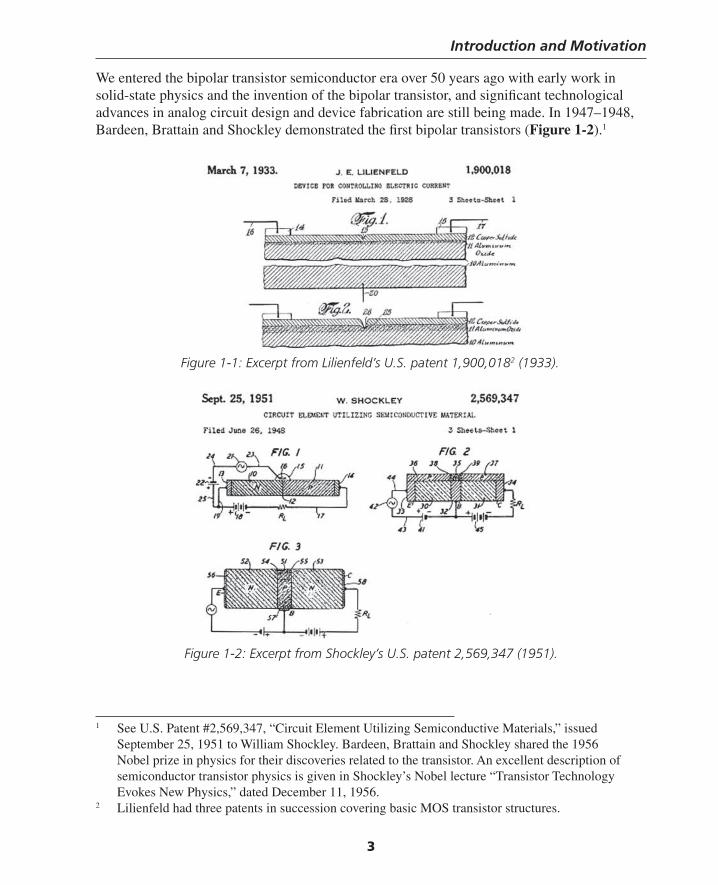
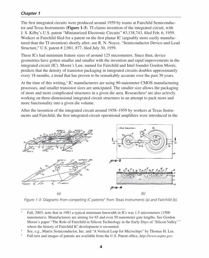
We entered the bipolar transistor semiconductor era over 50 years ago with early work in solid-state physics and the invention of the bipolar transistor, and signifi cant technological advances in analog circuit design and device fabrication are still being made. In 1947–1948, Bardeen, Brattain and Shockley demonstrated the fi rst bipolar transistors (Figure 1-2).1
1 See U.S. Patent #2,569,347, “Circuit Element Utilizing Semiconductive Materials,” issued September 25, 1951 to William Shockley. Bardeen, Brattain and Shockley shared the 1956 Nobel prize in physics for their discoveries related to the transistor. An excellent description of semiconductor transistor physics is given in Shockley’s Nobel lecture “Transistor Technology Evokes New Physics,” dated December 11, 1956.
2 Lilienfeld had three patents in succession covering basic MOS transistor structures.
Figure 1-1: Excerpt from Lilienfeld’s U.S. patent 1,900,0182 (1933).
Figure 1-2: Excerpt from Shockley’s U.S. patent 2,569,347 (1951).
Thompson Book.indb 3 3/20/2006 11:33:34 AM
Chapter 1
4
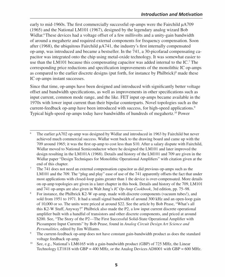
The fi rst integrated circuits were produced around 1959 by teams at Fairchild Semiconduc-tor and Texas Instruments (Figure 1-3). TI claims invention of the integrated circuit, with J. S. Kilby’s U.S. patent “Miniaturized Electronic Circuits” #3,138,743, fi led Feb. 6, 1959. Workers at Fairchild fi led for a patent on the fi rst planar IC (arguably more easily manufac-tured than the TI invention) shortly after; see R. N. Noyce, “Semiconductor Device-and-Lead Structure,” U.S. patent # 2,981, 877, fi led July 30, 1959.
These ICs had minimum feature sizes of around 125 micrometers. Since then, device geometries have gotten smaller and smaller with the invention and rapid improvements in the integrated circuit (IC). Moore’s Law, named for Fairchild and Intel founder Gordon Moore, predicts that the density of transistor packaging in integrated circuits doubles approximately every 18 months, a trend that has proven to be remarkably accurate over the past 30 years.
At the time of this writing,3 IC manufacturers are using 90-nanometer CMOS manufacturing processes, and smaller transistor sizes are anticipated. The smaller size allows the packaging of more and more complicated structures in a given die area. Researchers4 are also actively working on three-dimensional integrated circuit structures in an attempt to pack more and more functionality into a given die volume.
After the invention of the integrated circuit around 1958–1959 by workers at Texas Instru-ments and Fairchild, the fi rst integrated-circuit operational amplifi ers were introduced in the
(a) (b)
3 Fall, 2003; note that in 1983 a typical minimum linewidth in ICs was 1.5 micrometers (1500 nanometers). Manufacturers are aiming for 65 and even 50 nanometer gate lengths. See Gordon Moore’s paper “The Role of Fairchild in Silicon Technology in the Early Days of ‘Silicon Valley’ ” where the history of Fairchild IC development is recounted.
4 See, e.g., Matrix Semiconductor, Inc. and “A Vertical Leap for Microchips” by Thomas H. Lee.5 Full text and images of patents are available from the U.S. Patent offi ce, http://www.uspto.gov.
Figure 1-3: Diagrams from competing IC patents5 from Texas Instruments (a) and Fairchild (b).
Thompson Book.indb 4 3/20/2006 11:33:35 AM
Introduction and Motivation
5
early to mid-1960s. The fi rst commercially successful op-amps were the Fairchild µA709 (1965) and the National LM101 (1967), designed by the legendary analog wizard Bob Widlar.6 These devices had a voltage offset of a few millivolts and a unity-gain bandwidth of around a megahertz and required external components for frequency compensation. Soon after (1968), the ubiquitous Fairchild µA741, the industry’s fi rst internally compensated op-amp, was introduced and became a bestseller. In the 741, a 30-picofarad compensating ca-pacitor was integrated onto the chip using metal-oxide technology. It was somewhat easier to use than the LM101 because this compensating capacitor was added internal to the IC.7 The corresponding price reductions and specifi cation improvements of the monolithic IC op-amps as compared to the earlier discrete designs (put forth, for instance by Philbrick)8 made these IC op-amps instant successes.
Since that time, op-amps have been designed and introduced with signifi cantly better voltage offset and bandwidth specifi cations, as well as improvements in other specifi cations such as input current, common mode range, and the like. FET input op-amps became available in the 1970s with lower input current than their bipolar counterparts. Novel topologies such as the current-feedback op-amp have been introduced with success, for high-speed applications.9 Typical high-speed op-amps today have bandwidths of hundreds of megahertz.10 Power
6 The earlier µA702 op-amp was designed by Widlar and introduced in 1963 by Fairchild but never achieved much commercial success. Widlar went back to the drawing board and came up with the 709 around 1965; it was the fi rst op-amp to cost less than $10. After a salary dispute with Fairchild, Widlar moved to National Semiconductor where he designed the LM101 and later improved the design resulting in the LM101A (1968). Details and history of the LM101 and 709 are given in the Widlar paper “Design Techniques for Monolithic Operational Amplifi ers” with citation given at the end of this chapter.
7 The 741 does not need an external compensation capacitor as did previous op-amps such as the LM101 and the 709. The “plug and play” ease of use of the 741 apparently offsets the fact that under most applications with closed-loop gains greater than 1 the device is over-compensated. More details on op-amp topologies are given in a later chapter in this book. Details and history of the 709, LM101 and 741 op-amps are also given in Walt Jung’s IC Op-Amp Cookbook, 3rd edition, pp. 75–98.
8 For instance, the Philbrick K2-W op-amp, made with discrete components (vacuum tubes!), and sold from 1951 to 1971. It had a small signal bandwidth of around 300 kHz and an open-loop gain of 10,000 or so. The units were priced at around $22. See the article by Bob Pease, “What’s all this K2-W Stuff, Anyway?” Philbrick also made the P2, a low input current discrete operational amplifi er built with a handful of transistors and other discrete components, and priced at around $200. See, “The Story of the P2—The First Successful Solid-State Operational Amplifi er with Picoampere Input Currents” by Bob Pease, found in Analog Circuit Design Art Science and Personalities, edited by Jim Williams.
9 The current-feedback op-amp does not have constant gain-bandwidth product as does the standard voltage feedback op-amp.
10 See, e.g., National’s LM6165 with a gain-bandwidth product (GBP) of 725 MHz, the Linear Technology LT1818 with GBP = 400 MHz, or the Analog Devices AD8001 with GBP = 600 MHz.
Thompson Book.indb 5 3/20/2006 11:33:36 AM
Chapter 1
6
op-amps11 exist that can drive speakers or other heavy resistive or inductive loads with several amperes of load current. Low-power op-amps with sub-milliwatt standby power dissipation are now commonplace. Rail-to-rail op-amps are now available.
These advances have opened new applications and product markets for devices based on ana-log and digital signal processing. Currently, cellular telephone, cable television, and wireless internet technologies are driving the business in RF analog circuit design and miniature hand-held power electronics. Low-power devices enable the design of battery-powered devices with long battery life.
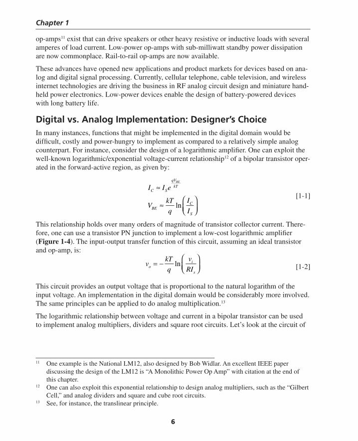
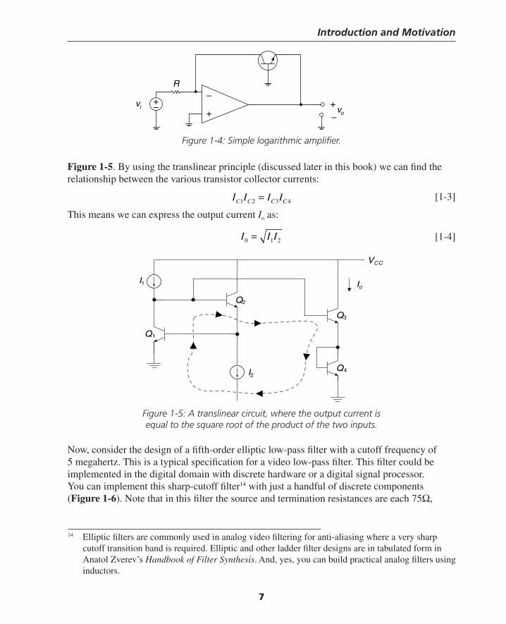
Digital vs. Analog Implementation: Designer’s ChoiceIn many instances, functions that might be implemented in the digital domain would be diffi cult, costly and power-hungry to implement as compared to a relatively simple analog counterpart. For instance, consider the design of a logarithmic amplifi er. One can exploit the well-known logarithmic/exponential voltage-current relationship12 of a bipolar transistor oper-ated in the forward-active region, as given by:
I I e
VkT
q
I
I
C S
qV
kT
BEC
S
BE
≈
≈⎛⎝⎜
⎞⎠⎟
ln [1-1]
This relationship holds over many orders of magnitude of transistor collector current. There-fore, one can use a transistor PN junction to implement a low-cost logarithmic amplifi er (Figure 1-4). The input-output transfer function of this circuit, assuming an ideal transistor and op-amp, is:
vkT
q
v
RIoi
s
= −⎛⎝⎜
⎞⎠⎟
ln [1-2]
This circuit provides an output voltage that is proportional to the natural logarithm of the input voltage. An implementation in the digital domain would be considerably more involved. The same principles can be applied to do analog multiplication.13
The logarithmic relationship between voltage and current in a bipolar transistor can be used to implement analog multipliers, dividers and square root circuits. Let’s look at the circuit of
11 One example is the National LM12, also designed by Bob Widlar. An excellent IEEE paper discussing the design of the LM12 is “A Monolithic Power Op Amp” with citation at the end of this chapter.
12 One can also exploit this exponential relationship to design analog multipliers, such as the “Gilbert Cell,” and analog dividers and square and cube root circuits.
13 See, for instance, the translinear principle.
Thompson Book.indb 6 3/20/2006 11:33:36 AM
Introduction and Motivation
7
Figure 1-5. By using the translinear principle (discussed later in this book) we can fi nd the relationship between the various transistor collector currents:
I I I IC C C C1 2 3 4= [1-3]
This means we can express the output current Io as:
I I I0 1 2= [1-4]
−
++
−vo
+vi −
R
Figure 1-5: A translinear circuit, where the output current is equal to the square root of the product of the two inputs.
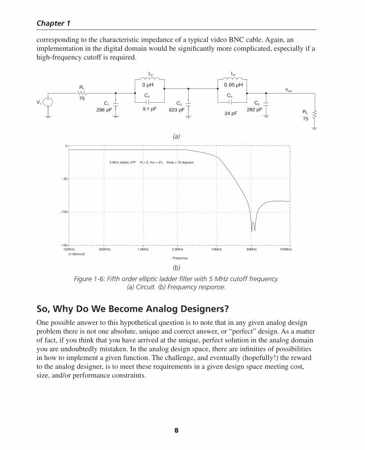
Now, consider the design of a fi fth-order elliptic low-pass fi lter with a cutoff frequency of 5 megahertz. This is a typical specifi cation for a video low-pass fi lter. This fi lter could be implemented in the digital domain with discrete hardware or a digital signal processor. You can implement this sharp-cutoff fi lter14 with just a handful of discrete components (Figure 1-6). Note that in this fi lter the source and termination resistances are each 75Ω,
I1
Q1
Q2
Q4
Q3
VCC
I2
Io
14 Elliptic fi lters are commonly used in analog video fi ltering for anti-aliasing where a very sharp cutoff transition band is required. Elliptic and other ladder fi lter designs are in tabulated form in Anatol Zverev’s Handbook of Filter Synthesis. And, yes, you can build practical analog fi lters using inductors.
Figure 1-4: Simple logarithmic amplifi er.
Thompson Book.indb 7 3/20/2006 11:33:36 AM
Chapter 1
8
corresponding to the characteristic impedance of a typical video BNC cable. Again, an implementation in the digital domain would be signifi cantly more complicated, especially if a high-frequency cutoff is required.
(a)
V1
R1
C1
75
296 pFC3
623 pF
C2
L2
3 µH
9.1 pFC5
282 pF24 pF
vout
C4
L4
0.95 µH
RL
75
0
−50
−100
−150
5 MHz elliptic LPF N = 5, rho = 4% theta = 16 degrees
100KHz 300KHz 1.0MHz 3.0MHz 10MHz 30MHz 100MHz� vdb(vout)
Frequency
(b)
Figure 1-6: Fifth order elliptic ladder fi lter with 5 MHz cutoff frequency.(a) Circuit. (b) Frequency response.
So, Why Do We Become Analog Designers?One possible answer to this hypothetical question is to note that in any given analog design problem there is not one absolute, unique and correct answer, or “perfect” design. As a matter of fact, if you think that you have arrived at the unique, perfect solution in the analog domain you are undoubtedly mistaken. In the analog design space, there are infi nities of possibilities in how to implement a given function. The challenge, and eventually (hopefully!) the reward to the analog designer, is to meet these requirements in a given design space meeting cost, size, and/or performance constraints.
Thompson Book.indb 8 3/20/2006 11:33:37 AM

Introduction and Motivation
9
Note on Nomenclature in this TextIn this text, there is a nomenclature that is used with regard to signals. In general, a transistor terminal voltage in an operating amplifi er has a DC operating point and a small-signal varia-tion about that operating point. The nomenclature used in the case of a transistor base-emitter voltage is:
v V vBE BE be= + [1-5]
where vBE (small “v” and capital “BE”) is the total variable, VBE (capital “V” and capital “BE”) is the DC operating point, and vbe (small “v” and small “be”) is the small-signal variation.
Note on Coverage in this BookIt is impossible to cover all aspects of analog design in a single textbook. Rather, in this text I have attempted to provide a potpourri of important techniques, tricks and analysis tools that I have found useful in designing real-world analog circuits. Where necessary, mathemati-cal derivations for theoretical techniques are given. In other areas, intuitive techniques and analogies are used to “map” solutions from one design domain to the analog design domain, hopefully bypassing extensive mathematical derivations.
There are several important subjects that are conspicuously not covered in this text, including:
• Noise
• JFET amplifi ers
• Switched capacitor fi lters
Other references, including textbooks and scholarly journals, have been provided at the end of each chapter for the reader to explore the topics in more depth. The author has provided explanatory notes including opinions with some of the citations.
It is assumed that the reader has a familiarity with Laplace transforms, pole-zero plots, Bode plots, the concept of system step response, and a basic understanding of differential equa-tions. Chapter 2 of this book reviews these signal processing basics. These fundamentals are needed to foster understanding of the more advanced topics in later chapters.
Thompson Book.indb 9 3/20/2006 11:33:37 AM
Chapter 1
10
ReferencesAnalog Devices, Nonlinear Circuits Handbook, Analog Devices, 1976. Good coverage of
logarithmic amplifi ers and other nonlinear analog circuits.Bardeen, J., and Brattain, W. H., “The Transistor, A Semiconductor Triode,” Physical Review,
vol. 74, no. 2, pp. 230–231, July 15, 1948, reprinted in Proceedings of the IEEE, vol. 86, no. 1, January 1998, pp. 29–30.
Bondyopadhyay, Probir, “In the Beginning,” Proceedings of the IEEE, vol. 86, no. 1, January 1998, pp. 63–77.
———, “W = Shockley, the Transistor Pioneer—Portrait of an Inventive Genius,” Proceed-ings of the IEEE, vol. 86, no. 1, January 1998, pp. 191–217.
Brinkman, William, Haggan, Douglas, and Troutman,William, “A History of the Invention of the Transistor and Where It Will Lead Us,” IEEE Journal of Solid-State Circuits, vol. 32, no. 12, December 1997, pp. 1858–1865.
Brinkman, William, “The Transistor: 50 Glorious Years and Where We Are Going,” 1997 IEEE International Solid-State Circuits Conference, Feb. 6–8, 1997, pp. 22–26.
Fullagar, Dave, “A New High Performance Monolithic Operational Amplifi er,” Fairchild Ap-plication Brief, May 1968. Description of the 741 op-amp by its designer.
Jung, Walter, IC Op-Amp Cookbook, 3rd edition, SAMS, 1995.Kilby, Jack, “The Integrated Circuit’s Early History,” Proceedings of the IEEE, vol. 88, no. 1,
January 2000, pp. 109–111.Lee, Thomas H., “A Vertical Leap for Microchips,” Scientifi c American, January 13, 2002.
This note describes Matrix Technologies’ efforts and motivation for producing 3D integrated circuits.
Manglesdorf, C., “The Changing Face of Analog IC Design,” IEEE Transactions on Funda-mentals, E85-A, no. 2, February 2002, pp. 282–285.
———, “The Future Role of the Analog Designer,” ISSCC 93, session WE3, pp. 78–79.Melliar-Smith, C. Mark, Borrus, Michael G., Haggan, Douglas, Lowrey, Tyler, Sangiovanni-
Vincentelli, Alberto, and Troutman, William, “The Transistor: An Invention Becomes a Big Business,” Proceedings of the IEEE, vol. 86, no. 1, January 1998, pp. 86–110.
Moore, Gordon, “The Role of Fairchild in Silicon Technology in the Early Days of “Silicon Valley,” Proceedings of the IEEE, vol. 86, no. 1, January 1998, pp. 53–62.
———, “Cramming More Components onto Integrated Circuits,” Electronics, April 19, 1965, pp. 114–117. The original paper where “Moore’s Law” was fi rst published.
National Semiconductor, “Log Converters,” National Application Note AN-30.———, Linear Applications Handbook.Pearson, G. L., and Brattain, W. H., “History of Semiconductor Research,” Proceedings of the
IRE, vol. 43, no. 12, December 1955, pp. 1794–1806.Pease, Bob, “What’s All This K2-W Stuff, Anyhow?,” Electronic Design, January 6, 2003.
Thompson Book.indb 10 3/20/2006 11:33:38 AM

Introduction and Motivation
11
———,“The Story of the P2—The First Successful Solid-State Operational Amplifi er with Picoampere Input Currents,” found in Analog Circuit Design: Art, Science and Personali-ties, pp. 67–78, edited by Jim Williams, Butterworth-Heinemann, 1991. A history and description of the K2-W operational amplifi er, a discrete op-amp sold in the 50s and 60s by Philbrick, and built with vacuum tubes, and the P2, a discrete-transistor Philbrick operational amplifi er.
Pease, Robert, Troubleshooting Analog Circuits, Butterworth-Heinemann, 1991.Perry, T. S., “For the Record: Kilby and the IC,” IEEE Spectrum, vol. 25, no. 13, December
1988, pp. 40–41. Description of the history of Kilby’s invention.Sah, Chih-Tang, “Evolution of the MOS Transistor—From Conception to VLSI,” Proceedings
of the IEEE, vol. 76, no. 10, October 1988, pp. 1280–1326Schaller, Robert, “Moore’s Law: Past, Present and Future,” IEEE Spectrum, vol. 34,
no. 6, June 1997, pp. 52–59.Shockley, William, “Transistor Technology Evokes New Physics,” 1956 Physics Nobel Prize
Lecture, December 11, 1956. ———, “Transistor Electronics—Imperfections, Unipolar and Analog Transistors,” Proceed-
ings of the IEEE, vol. 85, no. 12, December 1997, pp. 2055–2080. ———, “Theory of p-n Junctions in Semiconductors and p-n Junction Transistors,” Bell Sys-
tem Technical Journal, vol. 28, no. 7, July 1949, pp. 436–489. ———, “Electrons, Holes and Traps,” Proceedings of the IRE, vol. 46, no. 6, June 1958, pp.
973–990.Siebert, William McC., Circuits, Signals and Systems, McGraw-Hill, 1986.Small, James, “General-Purpose Electronic Analog Computing: 1945–1965,” IEEE Annals of
the History of Computing, vol. 15, no. 2, 1993, pp. 8–18.Soloman, James, “A Tribute to Bob Widlar,” IEEE Journal of Solid State Circuits,
vol. 26, no. 8, August 1991, pp. 1087–1089. Tribute and anecdotes about Bob Widlar.Sporck, Charles, and Molay, Richard L., Spinoff: A Personal History of the Industry that
Changed the World, Saranac Lake Publishing, 2001.Sugii, Toshihiro, Watanabe, Kiyoshi, and Sugatani, Shinji, “Transistor Design for 90-nm Gen-
eration and Beyond,” Fujitsu Science and Technology Journal, vol. 39, no. 1, June 2003, pp. 9–22.
United States Patent Offi ce, website: http://www.uspto.gov.Warner, Raymond, “Microelectronics: Its Unusual Origin and Personality,” IEEE Transac-
tions on Electron Devices, vol. 48, no. 11, November 2001, pp. 2457–2467.Widlar, Robert J., “Design Techniques for Monolithic Operational Amplifi ers,” IEEE Journal
of Solid State Circuits, vol. SC-4, no. 4, August 1969, pp. 184–191. Describes in detail the designs of the 709 and LM101A op-amps.
———, “Monolithic Op Amp—The Universal Linear Component,” National Semiconductor Linear Applications Handbook, Application Note no. AN-4.
Thompson Book.indb 11 3/20/2006 11:33:38 AM
Chapter 1
12
Widlar, Robert J., and Yamatake, Mineo, “A Monolithic Power Op-Amp,” IEEE Journal of Solid State Circuits, vol. 23, no. 2, April 1988. A detailed description of the design and operation of the LM12, an integrated circuit power op-amp designed in the 1980s. Appli-cations of the LM12 are given in National application note AN-446, “A 150W IC Op Amp Simplifi es Design of Power Circuits,” also written by Widlar and Yamatake.
Williams, Arthur B., and Taylor, Fred J., Electronic Filter Design Handbook LC, Active and Digital Filters, 2nd edition, McGraw-Hill, 1988.
Williams, Jim, Editor, The Art and Science of Analog Circuit Design, Butterworth-Heine-mann, 1998.
———, Analog Circuit Design: Art, Science and Personalities, Butterworth-Heinemann, 1991. These books edited by Jim Williams present a potpourri of design tips, tricks, and personal histories by some of the most noteworthy analog designers in the world.
Zverev, A., Handbook of Filter Synthesis, John Wiley, 1967. An excellent overview of analog ladder fi lter design with special emphasis on Butterworth, Bessel, Chebyshev and elliptic implementations. Lowpass to highpass and lowpass to bandpass transformations are also discussed in detail.
U.S. Patents15
Bardeen, J., and Brattain, W. H., “Three-Electrode Circuit Element Utilizing Semiconductive Materials,” U.S. Patent # 2,524,035, fi led June 7, 1948; issued October 3, 1950.
Kilby, J. S., “Miniaturized Electronic Circuits,” U.S. Patent # 3,138,743, fi led February 6, 1959; issued June 23, 1964.
Lilienfeld, J., “Method and Apparatus for Controlling Electric Currents,” U.S. Patent # 1,745,175, fi led October 8, 1926; issued January 28, 1930; “Amplifi er for Electric Cur-rents,” U.S. Patent # 1,877,140, fi led December 8, 1928; issued September 13, 1932; “Device for Controlling Electric Current,” U.S. Patent # 1,900,018, fi led March 28, 1928; issued March 7, 1933.
Noyce, R. N., “Semiconductor Device-and-Lead Structure,” U.S. Patent # 2,981,877, fi led July 30, 1959; issued April 25, 1961.
Shockley, W., “Circuit Element Utilizing Semiconductive Materials,” U.S. Patent # 2,569,347, fi led June 17, 1948; issued October 3, 1950; “Semiconductor Amplifi er,” U.S. Patent # 2,502,488, fi led September 24, 1948; issued April 5, 1950, reprinted in Proceedings of the IEEE, vol. 86, no. 1, January 1998, pp. 34–36.
15 All patents listed are available on the U.S. Patent and Trademark website: www.uspto.gov.
Thompson Book.indb 12 3/20/2006 11:33:38 AM
13
C H A P T E R 2Review of Signal-Processing Basics
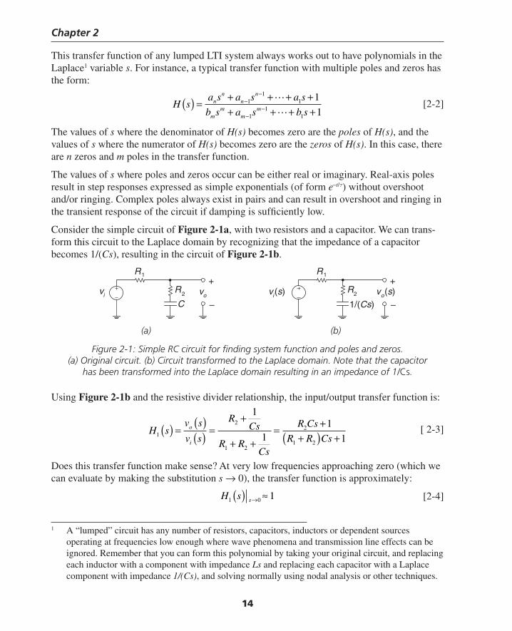
Review of Laplace Transforms, Transfer Functions and Pole-Zero PlotsThe transfer function and pole-zero plot of any linear time-invariant (LTI) system can be found by replacing all electronic components with their impedance expressed in the Laplace domain. For instance, the transformation from the circuit domain to the Laplace (or s) domain is made by making the following substitutions of circuit elements:
Circuit domain Laplace (s) domain
Resistance, R RInductance L Ls
Capacitance C1
Cs
The resultant transformed circuit also expresses a differential equation; the differential equa-tion can be found by making the substitution:
sd
dt⇒ [2-1]
In This Chapter
In this chapter, the basics of signal processing and analysis are covered. The important tools offered in this chapter such as transfer functions in the Laplace domain, the concept of poles and zeros, step and impulse responses, and Bode plots are reviewed and needed by the reader in later chapters.
Thompson Book.indb 13 3/20/2006 11:33:38 AM
Chapter 2
14
This transfer function of any lumped LTI system always works out to have polynomials in the Laplace1 variable s. For instance, a typical transfer function with multiple poles and zeros has the form:
H sa s a s a s
b s a s b sn
nn
n
mm
mm( ) =
+ + + ++ + + +
−−
−−
11
1
11
1
1
1 [2-2]
The values of s where the denominator of H(s) becomes zero are the poles of H(s), and the values of s where the numerator of H(s) becomes zero are the zeros of H(s). In this case, there are n zeros and m poles in the transfer function.
The values of s where poles and zeros occur can be either real or imaginary. Real-axis poles result in step responses expressed as simple exponentials (of form e–t/τ) without overshoot and/or ringing. Complex poles always exist in pairs and can result in overshoot and ringing in the transient response of the circuit if damping is suffi ciently low.
Consider the simple circuit of Figure 2-1a, with two resistors and a capacitor. We can trans-form this circuit to the Laplace domain by recognizing that the impedance of a capacitor becomes 1/(Cs), resulting in the circuit of Figure 2-1b.
1 A “lumped” circuit has any number of resistors, capacitors, inductors or dependent sources operating at frequencies low enough where wave phenomena and transmission line effects can be ignored. Remember that you can form this polynomial by taking your original circuit, and replacing each inductor with a component with impedance Ls and replacing each capacitor with a Laplace component with impedance 1/(Cs), and solving normally using nodal analysis or other techniques.
(a) (b)
Figure 2-1: Simple RC circuit for fi nding system function and poles and zeros. (a) Original circuit. (b) Circuit transformed to the Laplace domain. Note that the capacitor
has been transformed into the Laplace domain resulting in an impedance of 1/Cs.
Using Figure 2-1b and the resistive divider relationship, the input/output transfer function is:
H sv s
v s
RCs
R RCs
R Cs
R R Cso
i1
2
1 2
2
1 2
1
11
1( ) = ( )
( ) =+
+ +=
++( ) +
[ 2-3]
Does this transfer function make sense? At very low frequencies approaching zero (which we can evaluate by making the substitution s → 0), the transfer function is approximately:
H s s1 0 1( ) ≈→ [2-4]
+
–
vo
R1
R2
C
+
–
vo(s)vi(s)
R1
1/(Cs)
R2vi
Thompson Book.indb 14 3/20/2006 11:33:38 AM
Review of Signal-Processing Basics
15
This makes sense, since the capacitor becomes an open-circuit at zero frequency and the entire input signal is passed through to the output. At very high frequencies, (or when s → ∞) the capacitor shorts out and the transfer function is approximately:
H sR
R Rs12
1 2
( ) ≈+( )→∞ [2-5]
This also makes sense, since at very high frequencies this circuit looks like a simple voltage divider with R1 and R2. The pole and zero of H1(s) are found by:
sR R C
sR C
pole
zero
= −+( )
= −
1
11 2
2
[2-6]
The pole-zero plot for this transfer function is shown in Figure 2-2 below.
This same procedure can be used for more complicated circuits with any number of resistors, capacitors, inductors and dependent sources.
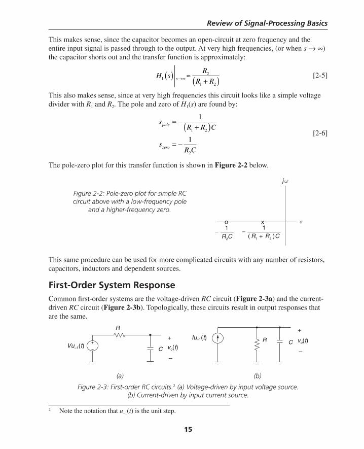
First-Order System ResponseCommon fi rst-order systems are the voltage-driven RC circuit (Figure 2-3a) and the current-driven RC circuit (Figure 2-3b). Topologically, these circuits result in output responses that are the same.
σ
ωj
xo
CRR )(1
21 +−
CR2
1−
Figure 2-2: Pole-zero plot for simple RC circuit above with a low-frequency pole
and a higher-frequency zero.
Vu−1(t) C
R
+
–
vo(t)
Iu−1(t)CR
+
–
vo(t)
(a) (b)
Figure 2-3: First-order RC circuits.2 (a) Voltage-driven by input voltage source. (b) Current-driven by input current source.
2 Note the notation that u–1(t) is the unit step.
Thompson Book.indb 15 3/20/2006 11:33:39 AM
Chapter 2
16
The step responses for the circuits are:
Voltage - driven RC
Current - dri
v t V e
i tV
Re
RC
ot
rt
( ) = −( )
( ) =
=
−
−
1 τ
τ
τvven RC
v t IR e
i t I e
RC
ot
rt
( ) = −( )( ) =
=
−
−
1 τ
τ
τ
[2-7]
The risetime of the voltage or current is defi ned as the time it takes the response to rise from 10% of fi nal value to 90% of fi nal value. For the fi rst-order system, this risetime is given by:
τ τR = 2 2. [2-8]
This defi nition of 10–90% risetime is shown in the step response of a generic lumped fi rst- order system in Figure 2-4.
The bandwidth is defi ned as the frequency at which the magnitude of the output response to an AC input signal drops to 70.7% (or –3dB) of the DC value. For the fi rst-order system, the transfer function can be expressed as:
H ss
H s
( ) =+
∠ ( ) = − ( )−
1
11
τωτtan
[2-9]
output
τRt
10.9
0.1
Figure 2-4: Unity step response of fi rst-order system showing 10–90% risetime.
Thompson Book.indb 16 3/20/2006 11:33:39 AM
Review of Signal-Processing Basics
17
We fi nd the –3dB bandwidth is:
ω
τωπ
h
hhf
=
=
1
2
[2-10]
where ωh is in radians per second and fh is in hertz. From these relationships, we can derive the relationship between bandwidth and risetime, which is exact for a fi rst-order system:
τRhf
=0 35. [2-11]
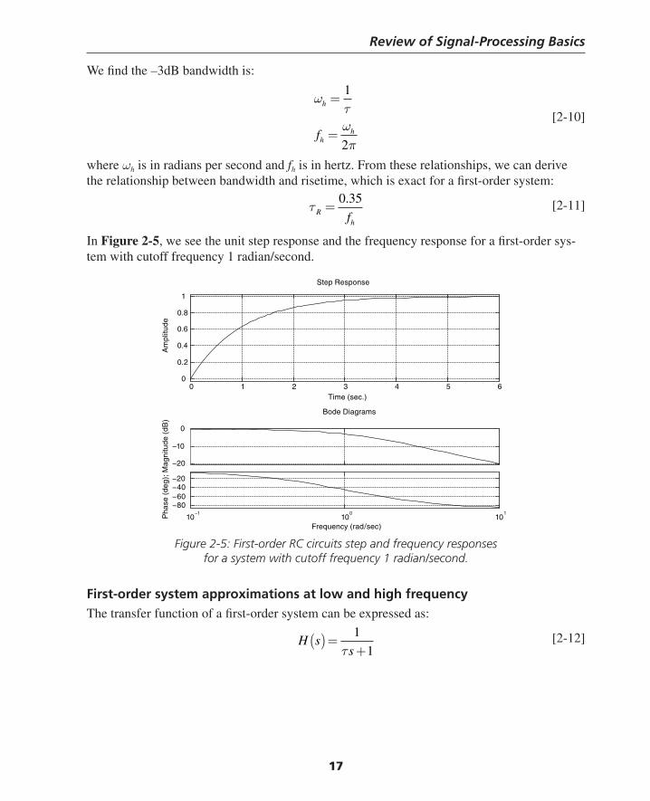
In Figure 2-5, we see the unit step response and the frequency response for a fi rst-order sys-tem with cutoff frequency 1 radian/second.
Figure 2-5: First-order RC circuits step and frequency responses for a system with cutoff frequency 1 radian/second.
First-order system approximations at low and high frequencyThe transfer function of a fi rst-order system can be expressed as:
H ss
( ) =+1
1τ [2-12]
Time (sec.)
Am
plitu
de
Step Response
0 1 2 3 4 5 60
0.2
0.4
0.6
0.8
1
Frequency (rad/sec)
Pha
se (
deg
); M
agni
tude
(dB
)
Bode Diagrams
−20
−10
0
10−1
100
101
−80−60−40−20
Thompson Book.indb 17 3/20/2006 11:33:39 AM
Chapter 2
18
where τ is the “time constant” of this fi rst-order system. The magnitude, angle and group delay3 of this transfer function are found by:
H jj
H j
H j
G jd H j
d
ωωτ
ωωτ
ω ωτ
ωω
( ) =+
( ) =( ) +
∠ ( ) = − ( )
( ) =− ∠ ( )
−
1
1
1
12
1tan
ωωτ
ωτ=
+( )12
[2-13]
Now, let’s note how this single pole behaves at low and high frequencies (where low and high are defi ned in relation to the pole frequency). For high frequencies, where ωτ >> 1, we can approximate the magnitude, phase and group delay of the transfer functions as:4
H j
H j
G j
ωωτ
ωωτ
ωω τ
ωτ
ωτ
ωτ
( )
∠ ( ) +
( )
1
1
1
1
1
1
≈
≈
≈
−π2
2
[2-14]
For high frequencies, the magnitude of the transfer function decreases proportionally with frequency, corresponding to a –20dB/decade rolloff. The angle approaches –π/2 radians, or –90 degrees. The group delay decreases with frequency; higher-frequency components are delayed less than lower-frequency components.
For low frequencies, where ωτ << 1, we can approximate the transfer functions as:5
H j
H j
G j
ω ωτ
ω ωτ
ω τ
ωτ
ωτ
ωτ
( ) ( )
∠ ( )( )
1
2
1
1
1
2≈ 1− ≈ 1
≈ −
≈
[2-15]
3 Group delay is a measure of how much time delay the frequency components in a signal undergo. Mathematically, the group delay of a system is the negative derivative of the phase with respect to omega. To fi nd group delay for the fi rst-order system, we make use of the identity: d
dxu
u
du
dxtan−( ) =
+1
2
1
14 We make use of several trigonometric identities here. For instance, the power series expansion for
arctangent is tan .− ( ) = − + ( ) >1 32 1 1 3 1x x x xπ -…for
5 Here we make use of the power series expansion: 1
11
21
+−
x
xx≈ for .
Thompson Book.indb 18 3/20/2006 11:33:40 AM
Review of Signal-Processing Basics
19
For low frequencies, the magnitude of the transfer function is approximately unity; however, there is some fi nite phase shift due to the pole. For instance, at a frequency ten times lower than the pole frequency, the pole contributes approximately –0.1 radians (or –5.7 degrees) of negative phase shift. Also, at frequencies much lower than the pole frequency, the negative phase shift is approximately linear with the frequency. This means that a high-frequency pole behaves approximately as a time delay, as shown by the group delay calculation. The negative phase shift can have consequences in, for instance, feedback loops where the extra phase shift can cause oscillations.
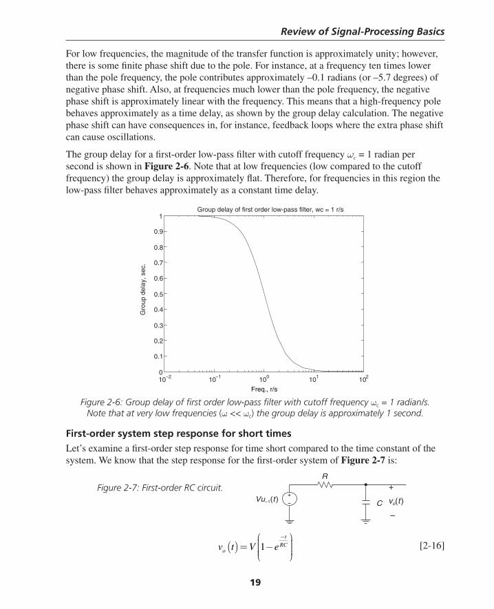
The group delay for a fi rst-order low-pass fi lter with cutoff frequency ωc = 1 radian per second is shown in Figure 2-6. Note that at low frequencies (low compared to the cutoff frequency) the group delay is approximately fl at. Therefore, for frequencies in this region the low-pass fi lter behaves approximately as a constant time delay.
First-order system step response for short timesLet’s examine a fi rst-order step response for time short compared to the time constant of the system. We know that the step response for the fi rst-order system of Figure 2-7 is:
10−2 10−1 100 101 1020
0.1
0.2
0.3
0.4
0.5
0.6
0.7
0.8
0.9
1
Freq., r/s
Group delay of first order low-pass filter, wc = 1 r/s
Gro
up d
elay
, sec
.
Vu−1(t ) C
R
+
–
vo(t )
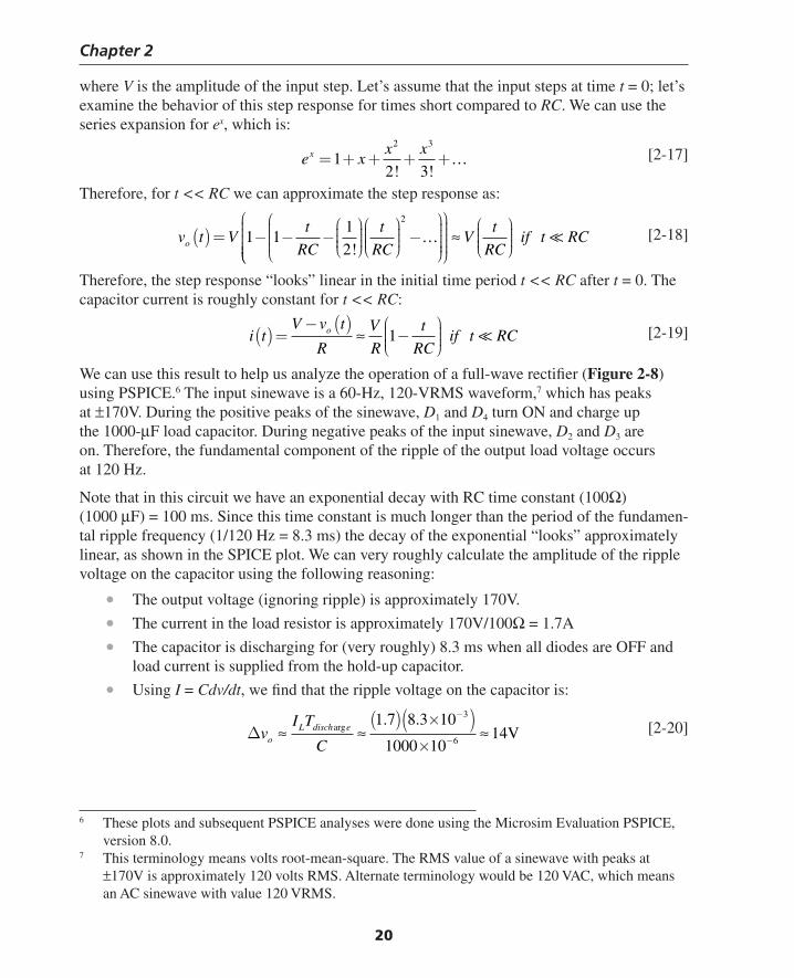
Figure 2-7: First-order RC circuit.
Figure 2-6: Group delay of fi rst order low-pass fi lter with cutoff frequency ωc = 1 radian/s. Note that at very low frequencies (ω << ωc) the group delay is approximately 1 second.
v t V eo
t
RC( ) = −⎛
⎝⎜⎜⎜⎜
⎞
⎠⎟⎟⎟⎟
−
1 [2-16]
Thompson Book.indb 19 3/20/2006 11:33:40 AM
Chapter 2
20
where V is the amplitude of the input step. Let’s assume that the input steps at time t = 0; let’s examine the behavior of this step response for times short compared to RC. We can use the series expansion for ex, which is:
e xx xx = + + + +12 3
2 3
! !… [2-17]
Therefore, for t << RC we can approximate the step response as:
v t Vt
RC
t
RCo ( ) = − − −⎛⎝⎜⎜⎜
⎞⎠⎟⎟⎟⎛⎝⎜⎜⎜
⎞⎠⎟⎟⎟ −
⎛
⎝
⎜⎜⎜⎜
⎞
⎠
⎟⎟⎟⎟⎟
⎛1 1
1
2
2
!…
⎝⎝
⎜⎜⎜⎜⎜
⎞
⎠
⎟⎟⎟⎟⎟
⎛⎝⎜⎜⎜
⎞⎠⎟⎟⎟≈ V
t
RCif t RC [2-18]
Therefore, the step response “looks” linear in the initial time period t << RC after t = 0. The capacitor current is roughly constant for t << RC:
i tV v t
R
V
R
t
RCif t RCo( ) =
− ( )−
⎛⎝⎜⎜⎜
⎞⎠⎟⎟⎟≈ 1 [2-19]
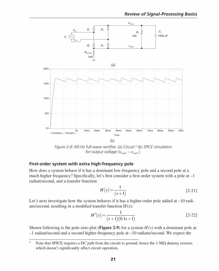
We can use this result to help us analyze the operation of a full-wave rectifi er (Figure 2-8) using PSPICE.6 The input sinewave is a 60-Hz, 120-VRMS waveform,7 which has peaks at ±170V. During the positive peaks of the sinewave, D1 and D4 turn ON and charge up the 1000-μF load capacitor. During negative peaks of the input sinewave, D2 and D3 are on. Therefore, the fundamental component of the ripple of the output load voltage occurs at 120 Hz.
Note that in this circuit we have an exponential decay with RC time constant (100Ω)(1000 μF) = 100 ms. Since this time constant is much longer than the period of the fundamen-tal ripple frequency (1/120 Hz = 8.3 ms) the decay of the exponential “looks” approximately linear, as shown in the SPICE plot. We can very roughly calculate the amplitude of the ripple voltage on the capacitor using the following reasoning:
• The output voltage (ignoring ripple) is approximately 170V.
• The current in the load resistor is approximately 170V/100Ω = 1.7A
• The capacitor is discharging for (very roughly) 8.3 ms when all diodes are OFF and load current is supplied from the hold-up capacitor.
• Using I = Cdv/dt, we fi nd that the ripple voltage on the capacitor is:
ΔvI T
oL disch e≈ ≈
1.7≈arg
.
C
( ) ×( )×
−
−
8 3 10
1000 10
3
614V [2-20]
6 These plots and subsequent PSPICE analyses were done using the Microsim Evaluation PSPICE, version 8.0.
7 This terminology means volts root-mean-square. The RMS value of a sinewave with peaks at ±170V is approximately 120 volts RMS. Alternate terminology would be 120 VAC, which means an AC sinewave with value 120 VRMS.
Thompson Book.indb 20 3/20/2006 11:33:41 AM
Review of Signal-Processing Basics
21
(a)
D1 D2
D4D3
Rdummy
1e6
vload–
Vload+
vin–
Vin+
V1
RL
100
CL
1000 µF
200V
150V
100V
50V
0V0s 10ms 20ms 30ms 40ms 50ms 60ms 70ms 80ms 90ms 100m
�V(vload+) − V(vload−)Time
(b)
Figure 2-8: 60-Hz full-wave rectifi er. (a) Circuit.8 (b) SPICE simulation for output voltage (vload+ – vload–).
First-order system with extra high-frequency poleHow does a system behave if it has a dominant low-frequency pole and a second pole at a much higher frequency? Specifi cally, let’s fi rst consider a fi rst-order system with a pole at –1 radian/second, and a transfer function:
H ss
( ) =+( )1
1 [2-21]
Let’s next investigate how the system behaves if it has a higher-order pole added at –10 radi-ans/second, resulting in a modifi ed transfer function H'(s):
′( ) =+( ) +( )
H ss s
1
1 0 1 1. [2-22]
Shown following is the pole-zero plot (Figure 2-9) for a system H'(s) with a dominant pole at –1 radian/second and a second higher-frequency pole at –10 radians/second. We expect the
8 Note that SPICE requires a DC path from the circuit to ground, hence the 1-MΩ dummy resistor, which doesn’t signifi cantly affect circuit operation.
Thompson Book.indb 21 3/20/2006 11:33:41 AM
Chapter 2
22
step response and frequency response of this system to be dominated by the pole at –1 radian/second. For instance, we expect a 10–90% risetime of ∼2.2 seconds, and a –3dB bandwidth of 1 radian/second.
σ
ωj
xx
τ2– 1
τ1– 1
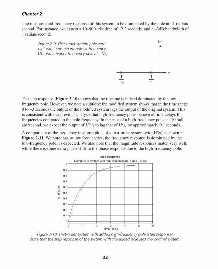
The step response (Figure 2-10) shows that the risetime is indeed dominated by the low- frequency pole. However, we note a subtlety: the modifi ed system shows that in the time range 0 to ~3 seconds the output of the modifi ed system lags the output of the original system. This is consistent with our previous analysis that high-frequency poles behave as time delays for frequencies compared to the pole frequency. In the case of a high-frequency pole at –10 radi-ans/second, we expect the output of H'(s) to lag that of H(s) by approximately 0.1 seconds.
A comparison of the frequency response plots of a fi rst-order system with H'(s) is shown in Figure 2-11. We note that, at low frequencies, the frequency response is dominated by the low-frequency pole, as expected. We also note that the magnitude responses match very well, while there is some extra phase shift in the phase response due to the high-frequency pole.
Figure 2-9: First-order system pole-zero plot with a dominant pole at frequency
–1/τ1 and a higher frequency pole at –1/τ2.
Time (sec.)
Am
plitu
de
Step Response
0 1 2 3 4 5 6
0
0.1
0.2
0.3
0.4
0.5
0.6
0.7
0.8
0.9
1Compare to system with real-axis poles at –1 and –10 r/s
Figure 2-10: First-order system with added high-frequency pole (step response). Note that the step response of the system with the added pole lags the original system.
Thompson Book.indb 22 3/20/2006 11:33:41 AM

Review of Signal-Processing Basics
23
Figure 2-11: First-order system pole-zero plot with added high-frequency pole (frequency response). Note that at frequencies below that of the low-frequency pole the two magnitude transfer functions match well.
Second-Order SystemsA second-order system is one in which there are two poles. For second-order systems consisting of resistors and capacitors (without any inductors or dependent sources), the poles lie on the real axis. For this special case, there is no possibility of overshoot or ringing in the step response.
Other second-order systems can be built with coupled, lumped energy-storage mechanisms or with dependent sources, which may result in overshoot and ringing in the transient response, provided that damping is not too high. Some examples of systems that may be potentially underdamped are:
• Mass and spring
• LC circuit
• Rotational inertia and torsional spring
• RC circuits with op-amp feedback
• Magnetic suspensions
Mass-spring systemA mass-spring system is shown in Figure 2-12. When this system vibrates, energy is alter-nately stored in the kinetic energy of the mass and in the stretch of the spring. If we consider y to be the displacement of the spring from free-hanging equilibrium, the force that the spring exerts on the mass is:
f kyy = − [2-23]
Newton’s law applied to the moving mass is:
f ky Md y
dty = − =2
2 [2-24]
Frequency (rad/sec)
Pha
se (
deg)
; Mag
nitu
de (
dB)
Compare to system with real-axis poles at –1 and –10 r/s
−60−50−40−30−20−10
0
10−1 100 101 102
−160−140−120−100−80−60−40−20
Thompson Book.indb 23 3/20/2006 11:33:42 AM
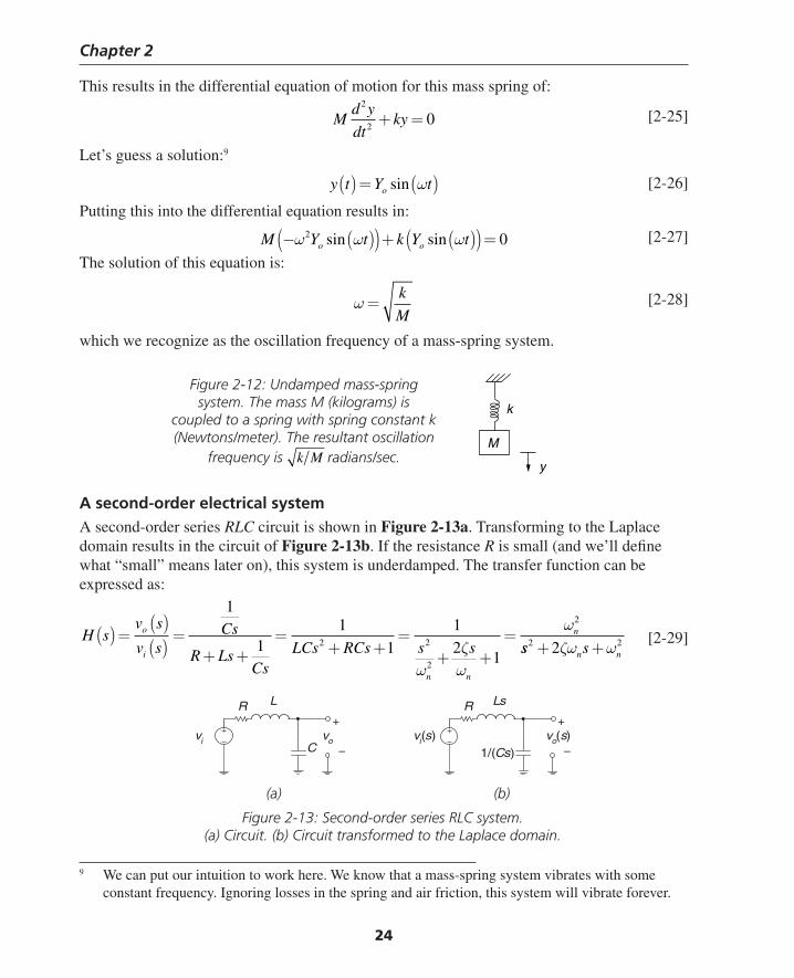
Chapter 2
24
This results in the differential equation of motion for this mass spring of:
Md y
dtky
2
20+ = [2-25]
Let’s guess a solution:9
y t Y to( ) = ( )sin ω [2-26]
Putting this into the differential equation results in:
M Y t k Y to o− ( )( )+ ( )( )=ω ω ω2 0sin sin [2-27]
The solution of this equation is:
ω =k
M [2-28]
which we recognize as the oscillation frequency of a mass-spring system.
9 We can put our intuition to work here. We know that a mass-spring system vibrates with some constant frequency. Ignoring losses in the spring and air friction, this system will vibrate forever.
k
y
M
vovi
R
C
L
vo(s)vi(s)
R
1/(Cs)
Ls
+
–
+
–
A second-order electrical systemA second-order series RLC circuit is shown in Figure 2-13a. Transforming to the Laplace domain results in the circuit of Figure 2-13b. If the resistance R is small (and we’ll defi ne what “small” means later on), this system is underdamped. The transfer function can be expressed as:
H s
v s
v sCs
R LsCs
LCs RCs s so
i
n n
n( ) =( )( )
=+ +
=+ +
=+ +
=
1
11
1
1
21
2 2
2
2
ωζ
ω
ωss sn n
2 22+ +ζω ω [2-29]
Figure 2-12: Undamped mass-spring system. The mass M (kilograms) is
coupled to a spring with spring constant k (Newtons/meter). The resultant oscillation
frequency is k M radians/sec.
(a) (b)
Figure 2-13: Second-order series RLC system. (a) Circuit. (b) Circuit transformed to the Laplace domain.
Thompson Book.indb 24 3/20/2006 11:33:42 AM
Review of Signal-Processing Basics
25
This equation has been put into second-order system standard form where ωn is the “natural frequency” of the circuit and ζ is the “damping ratio.” In the series RLC circuit, the natural frequency and damping ratio are:
ω
ω
n
n
o
LCRC R
L
C
R
Z
=
= = =
1
2
1
2
1
2ς
[2-30]
The natural frequency is an indication of the relative speed of response of the system, and the damping ratio tells you how oscillatory the step response will be, and how peaky the frequency response will be. Note that the damping ratio depends on the value of the series resistor R compared to Zo. In resonant LC circuits, this term Zo crops up again and again and hence is called the “characteristic impedance” of the resonant circuit.
The magnitude and phase of the frequency response are given by:
H j
j
H j
n
ωω
ωωω
ωω
ω
( ) =+ −
⎛
⎝⎜⎜⎜⎜
⎞
⎠⎟⎟⎟⎟
( ) =⎛
⎝⎜⎜⎜⎜
⎞
⎠⎟⎟⎟⎟
1
21
1
2
2
2
2
ς
ς
n
n
++ −⎛
⎝⎜⎜⎜⎜
⎞
⎠⎟⎟⎟⎟
∠ ( ) = −
⎛
⎝⎜⎜⎜⎜
⎞
⎠⎟⎟⎟⎟
−
−
1
2
2
2
2
1
ωω
ω
ωω
ωω
n
H j tan
ς
n
2
n
1 22
12 2
2⎛
⎝⎜⎜⎜⎜
⎞
⎠⎟⎟⎟⎟
= −−
⎛
⎝⎜⎜⎜⎜
⎞
⎠⎟⎟⎟⎟
−tanςωω
ω ωn
n
[2-31]
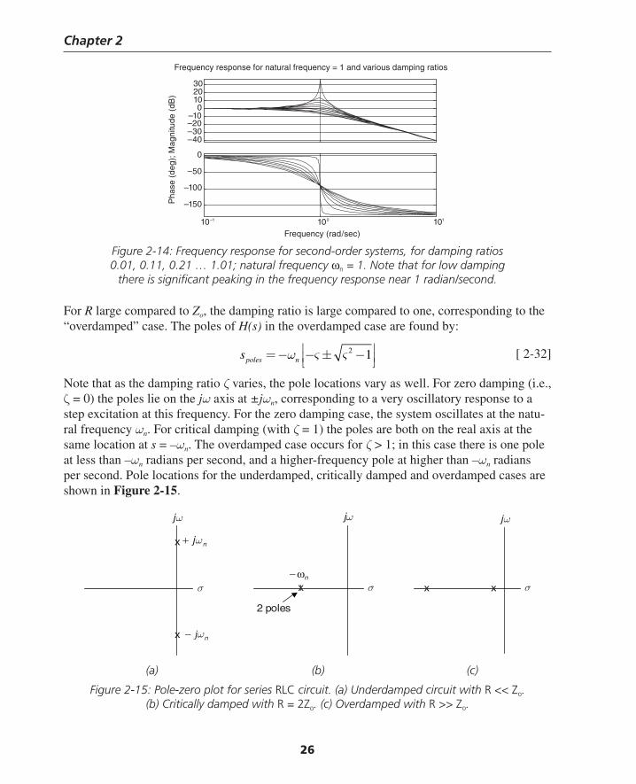
A plot of this transfer function magnitude and phase for varying values of damping ratio ζ is shown in Figure 2-14. Note that as the damping ratio decreases, the peak of the frequency response10 (which occurs at a frequency near ωn) increases.
10 We can show that the frequency at which the transfer function has its peak is:
ω ωp n for= −1 2 2ς ς < 0.707
This frequency is close to the natural frequency ωn if the damping ratio is small. The magnitude of the transfer function at this peak frequency is:
M forp =
−
1
2 1 2ς ςς < 0.707
Thompson Book.indb 25 3/20/2006 11:33:43 AM
Chapter 2
26
Figure 2-14: Frequency response for second-order systems, for damping ratios 0.01, 0.11, 0.21 … 1.01; natural frequency ωn = 1. Note that for low damping
there is signifi cant peaking in the frequency response near 1 radian/second.
For R large compared to Zo, the damping ratio is large compared to one, corresponding to the “overdamped” case. The poles of H(s) in the overdamped case are found by:
spoles n= − − ± −⎢⎣⎢
⎥⎦⎥
ω ς ς 2 1 [ 2-32]
Note that as the damping ratio ζ varies, the pole locations vary as well. For zero damping (i.e., ζ = 0) the poles lie on the jω axis at ±jωn, corresponding to a very oscillatory response to a step excitation at this frequency. For the zero damping case, the system oscillates at the natu-ral frequency ωn. For critical damping (with ζ = 1) the poles are both on the real axis at the same location at s = –ωn. The overdamped case occurs for ζ > 1; in this case there is one pole at less than –ωn radians per second, and a higher-frequency pole at higher than –ωn radians per second. Pole locations for the underdamped, critically damped and overdamped cases are shown in Figure 2-15.
σ
ωj
x njω+
x njω−
σ
ωj
xnω−
2 poles
σ
ωj
xx
Frequency (rad/sec)
Pha
se (
deg)
; Mag
nitu
de (
dB)
Frequency response for natural frequency = 1 and various damping ratios
–40–30–20–10
0102030
10–1 100 101
–150
–100
–50
0
(a) (b) (c)
Figure 2-15: Pole-zero plot for series RLC circuit. (a) Underdamped circuit with R << Zo. (b) Critically damped with R = 2Zo. (c) Overdamped with R >> Zo.
Thompson Book.indb 26 3/20/2006 11:33:43 AM
Review of Signal-Processing Basics
27
Now, what happens if we excite this system exactly at the natural frequency, or at ω = ωn? The response is:
H j
H j
n
n
ω
ω
ω ω
ω ω
( ) =
∠ ( ) = −
=
=
1
2
2
ςπ
[2-33]
For low damping ratio ζ, the frequency response shows a very peaky response at the natural frequency.
Quality factor “Q”Another commonly used metric for evaluating second-order systems is quality factor or “Q.” Quality factor is defi ned as:
ωE
Pstored
diss
[2-34]
where Estored is the peak stored energy in the system and Pdiss is the average power dissipation. First, let’s look at a series resonant network (Figure 2-16a). The calculation for quality factor at resonance is:
ω =
=
=
=⎛
⎝⎜⎜⎜
⎞
⎠⎟⎟⎟⎟
1
1
21
2
11212
2
2
2
LC
E LI
P I R
QLC
LI
stored pk
diss pk
pk
II R
L
CR
Z
Rpk
o
2
⎛
⎝
⎜⎜⎜⎜⎜⎜⎜⎜⎜
⎞
⎠
⎟⎟⎟⎟⎟⎟⎟⎟⎟⎟
= =
[2-35]
In the series resonant circuit, as resistance R increases, quality factor decreases. This is because a large resistor provides more damping.
(a) (b)
Figure 2-16: Resonant networks. (a) Series resonant RLC network. (b) Parallel resonant.
L R
C CRL
Thompson Book.indb 27 3/20/2006 11:33:44 AM
Chapter 2
28
Next, let’s consider a parallel RLC network (Figure 2-16b). The calculation for Q at resonance is:
ω =
=
=
=⎛
⎝⎜⎜⎜
⎞
⎠⎟⎟⎟⎟
1
1
2
1
2
11212
2
2
2
LC
E CV
PV
R
QLC
CV
stored pk
disspk
pk
VV
R
R
L
C
R
Zpk o2
⎛
⎝
⎜⎜⎜⎜⎜⎜⎜⎜⎜⎜
⎞
⎠
⎟⎟⎟⎟⎟⎟⎟⎟⎟⎟⎟
= =
[2-36]
In the parallel resonant circuit, a small resistor provides more damping.
Now, we see that quality factor is related to damping ratio by:
Q =1
2ς [2-37]
Let’s rewrite the previous equation for the transfer function of a series-resonant circuit, this time using quality factor:
H s
s s s s
Qn n n n
( ) =+ +
=+ +
1
21
1
12
2
2
2ωζ
ω ω ω [2-38]
The magnitude of this transfer function is:
H s
Qn n
( ) =
−⎛
⎝⎜⎜⎜⎜
⎞
⎠⎟⎟⎟⎟
+⎛
⎝⎜⎜⎜⎜
⎞
⎠⎟⎟⎟⎟
1
12
2
2 2ωω
ωω
[2-39]
At the natural frequency (ω = ωn), the magnitude of the transfer function is:
H s Qn
( ) ==ω ω
[2-40]
Transient response of second-order systemA second-order LCR system is shown in Figure 2-17. The input is a step vi(t) at time t = 0. Let’s assume, at fi rst, that the resistance is small enough so that the system is under-damped (i.e., that it has complex poles).
Thompson Book.indb 28 3/20/2006 11:33:44 AM
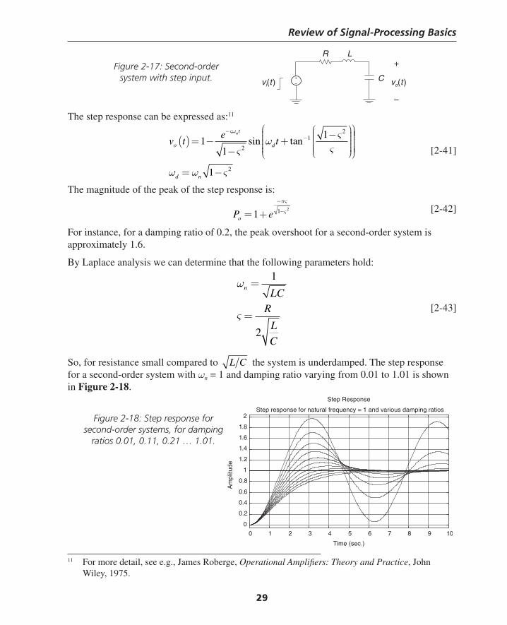
Review of Signal-Processing Basics
29
The step response can be expressed as:11
v t
eto
t
d
n
( ) = −−
+−⎛
⎝
⎜⎜⎜⎜⎜
⎞
⎠
⎟⎟⎟⎟⎟
⎛
⎝
⎜⎜⎜⎜⎜
⎞
⎠
−−1
1
12
12ς
ς
ςς
ω
ωsin tan⎟⎟⎟⎟⎟⎟⎟
= −ω ωd n 1 2ς
[2-41]
The magnitude of the peak of the step response is:
P eo = +−
1
πς
ς1− 2 [2-42]
For instance, for a damping ratio of 0.2, the peak overshoot for a second-order system is approximately 1.6.
By Laplace analysis we can determine that the following parameters hold:
ωnLC
R
L
C
=
=
1
2
ς [2-43]
So, for resistance small compared to L C the system is underdamped. The step response for a second-order system with ωn = 1 and damping ratio varying from 0.01 to 1.01 is shown in Figure 2-18.
C
R L
vo(t )vi(t )
+
–
Figure 2-17: Second-order system with step input.
11 For more detail, see e.g., James Roberge, Operational Amplifi ers: Theory and Practice, John Wiley, 1975.
Time (sec.)
Am
plitu
de
Step Response
0 1 2 3 4 5 6 7 8 9 10
0
0.2
0.4
0.6
0.8
1
1.2
1.4
1.6
1.8
2Step response for natural frequency = 1 and various damping ratios
Figure 2-18: Step response for second-order systems, for damping
ratios 0.01, 0.11, 0.21 … 1.01.
Thompson Book.indb 29 3/20/2006 11:33:44 AM
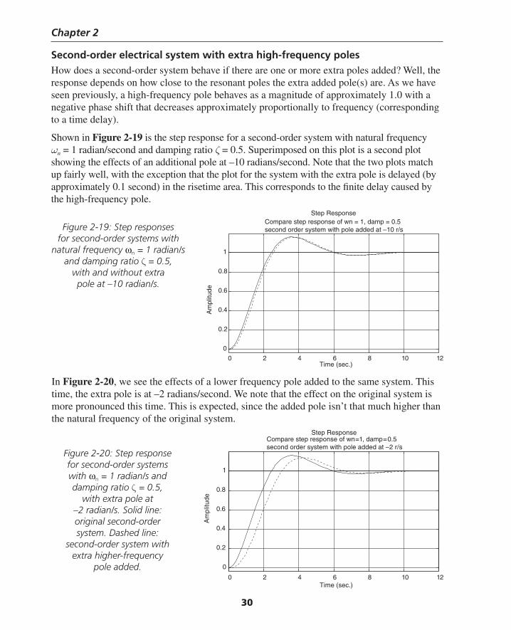
Chapter 2
30
Second-order electrical system with extra high-frequency polesHow does a second-order system behave if there are one or more extra poles added? Well, the response depends on how close to the resonant poles the extra added pole(s) are. As we have seen previously, a high-frequency pole behaves as a magnitude of approximately 1.0 with a negative phase shift that decreases approximately proportionally to frequency (corresponding to a time delay).
Shown in Figure 2-19 is the step response for a second-order system with natural frequency ωn = 1 radian/ second and damping ratio ζ = 0.5. Superimposed on this plot is a second plot showing the effects of an additional pole at –10 radians/second. Note that the two plots match up fairly well, with the exception that the plot for the system with the extra pole is delayed (by approximately 0.1 second) in the risetime area. This corresponds to the fi nite delay caused by the high-frequency pole.
In Figure 2-20, we see the effects of a lower frequency pole added to the same system. This time, the extra pole is at –2 radians/second. We note that the effect on the original system is more pronounced this time. This is expected, since the added pole isn’t that much higher than the natural frequency of the original system.
Time (sec.)
Am
plitu
deStep Response
0 2 4 6 8 10 12
0
0.2
0.4
0.6
0.8
1
Compare step response of wn = 1, damp = 0.5 second order system with pole added at –10 r/s
Time (sec.)
Am
plitu
de
Step Response
0 2 4 6 8 10 12
0
0.2
0.4
0.6
0.8
1
Compare step response of wn=1, damp=0.5 second order system with pole added at –2 r/s
Figure 2-19: Step responses for second-order systems with
natural frequency ωn = 1 radian/s and damping ratio ζ = 0.5,
with and without extra pole at –10 radian/s.
Figure 2-20: Step response for second-order systems with ωn = 1 radian/s and damping ratio ζ = 0.5,
with extra pole at –2 radian/s. Solid line: original second-order system. Dashed line:
second-order system with extra higher-frequency
pole added.
Thompson Book.indb 30 3/20/2006 11:33:45 AM
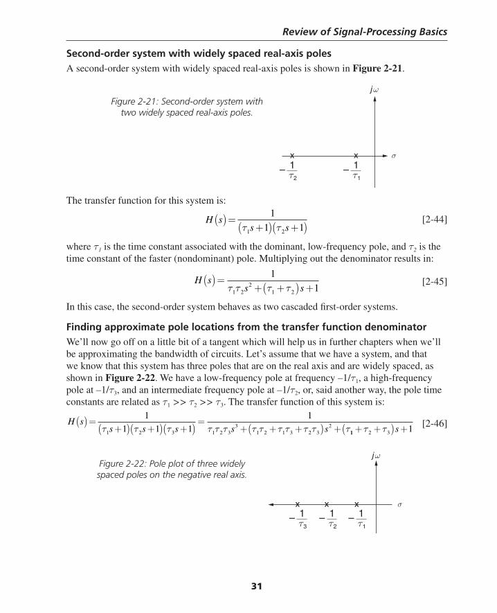
Review of Signal-Processing Basics
31
Second-order system with widely spaced real-axis polesA second-order system with widely spaced real-axis poles is shown in Figure 2-21.
The transfer function for this system is:
H ss s
( ) =+( ) +( )
1
1 11 2τ τ [2-44]
where τ1 is the time constant associated with the dominant, low-frequency pole, and τ2 is the time constant of the faster (nondominant) pole. Multiplying out the denominator results in:
H ss s
( ) =+ +( ) +
1
11 22
1 2τ τ τ τ [2-45]
In this case, the second-order system behaves as two cascaded fi rst-order systems.
Finding approximate pole locations from the transfer function denominator We’ll now go off on a little bit of a tangent which will help us in further chapters when we’ll be approximating the bandwidth of circuits. Let’s assume that we have a system, and that we know that this system has three poles that are on the real axis and are widely spaced, as shown in Figure 2-22. We have a low-frequency pole at frequency –1/τ1, a high-frequency pole at –1/τ3, and an intermediate frequency pole at –1/τ2, or, said another way, the pole time constants are related as τ1 >> τ2 >> τ3. The transfer function of this system is:
H ss s s s s
( ) =+( ) +( ) +( )
=+ + +( ) +
1
1 1 1
1
1 2 3 1 2 33
1 2 1 3 2 32τ τ τ τ τ τ τ τ τ τ τ τ τ11 2 3 1+ +( ) +τ τ s [2-46]
σ
ωj
xx
τ2– 1
τ1– 1
Figure 2-21: Second-order system with two widely spaced real-axis poles.
σ
ωj
xxx
τ3– 1
τ2– 1
τ1– 1
Figure 2-22: Pole plot of three widely spaced poles on the negative real axis.
Thompson Book.indb 31 3/20/2006 11:33:46 AM
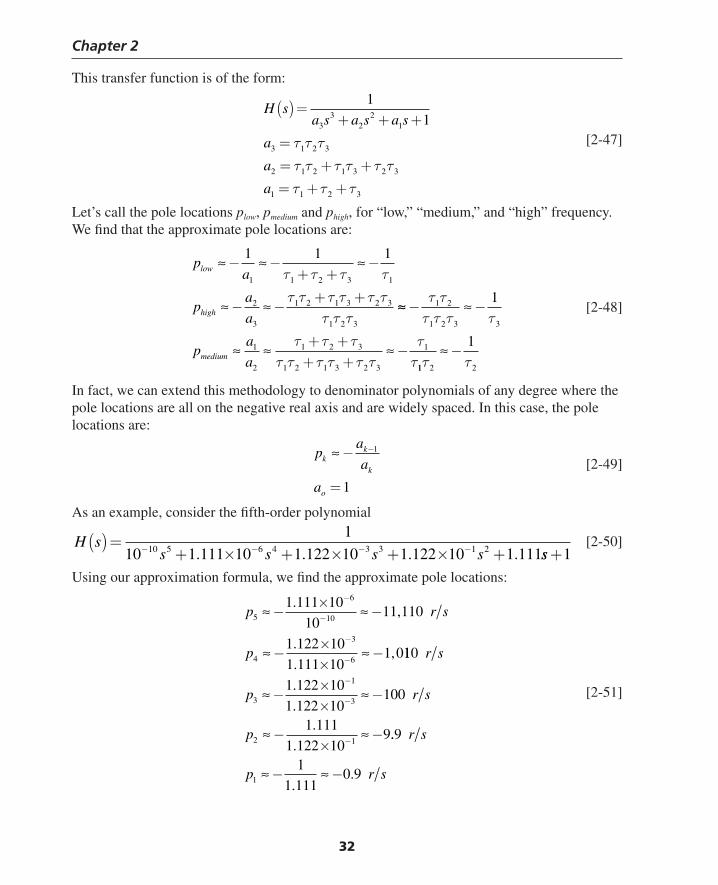
Chapter 2
32
This transfer function is of the form:
H s
a s a s a s
a
a
a
( ) =+ + +
=
= + +
= + +
1
133
22
1
3 1 2 3
2 1 2 1 3 2 3
1 1 2 3
τ τ τ
τ τ τ τ τ τ
τ τ τ
[2-47]
Let’s call the pole locations plow, pmedium and phigh, for “low,” “medium,” and “high” frequency. We fi nd that the approximate pole locations are:
pa
pa
a
low
high
≈ ≈ ≈
≈ ≈
− −+ +
−
− −+ +
1 1 1
1 1 2 3 1
2
3
1 2 1 3 2 3
1 2 3
τ τ τ τ
τ τ τ τ τ ττ τ τ
≈≈ ≈
≈ ≈ ≈
− −
+ ++ +
−
τ ττ τ τ τ
τ τ ττ τ τ τ τ τ
ττ
1 2
1 2 3 3
1
2
1 2 3
1 2 1 3 2 3
1
1
pa
amedium11 2 2
1
τ τ≈ −
[2-48]
In fact, we can extend this methodology to denominator polynomials of any degree where the pole locations are all on the negative real axis and are widely spaced. In this case, the pole locations are:
p
a
a
a
kk
k
o
≈ −
=
−1
1
[2-49]
As an example, consider the fi fth-order polynomial
H ss s s s
( ) =+ × + × + × +− − − −
1
10 1 111 10 1 122 10 1 122 10 1 11110 5 6 4 3 3 1 2. . . . ss +1
[2-50]
Using our approximation formula, we fi nd the approximate pole locations:
p r s
p
5
6
10
4
3
6
1 111 10
10
1 122 10
1 111 10
≈ ≈
≈ ≈
−×
−××
−
−
−
−
.
.
.
−
−
11,110
1,0110
100
9
r s
p r s
p
3
1
3
2 1
1 122 10
1 122 101 111
1 122 10
≈ ≈
≈ ≈
−××
−×
−
−
−
.
..
.
−
− ..9
0.9
r s
p r s1
1
1 111≈ ≈−
.−
[2-51]
Thompson Book.indb 32 3/20/2006 11:33:46 AM
Review of Signal-Processing Basics
33
In this example, the actual pole locations12 are at –1, –10, –100, –1000 and –10000 radians per second. We fi nd that the methodology gives us a rough approximation of the pole locations if we’re correct in our initial assumption that the poles are on the real axis and are widely spaced.
Review of Resonant Electrical CircuitsConsider a parallel LC circuit as shown in Figure 2-23. This is a standard resonant circuit that will oscillate at frequency ωr as the energy sloshes back and forth between electric storage in the capacitor and magnetic storage in the inductor. Let’s assume that the initial condition in the circuit is that the inductor current is zero and the capacitor voltage is some voltage vc. The current in the inductor is given by the differential equation:
di
dt
v
LL c= [2-52]
Similarly, the voltage on the capacitor can be found by:
dv
dt
i
Cc L=
− [2-53]
We can solve for the voltage on the capacitor v(t) by differentiating the capacitor equation and substituting for di/dt, resulting in:
d v
dt C
di
dt
v
LCc L c
2
2
1= − = − [2-54]
Now, we can fi nd the resonant frequency by guessing that the voltage v(t) is sinusoidal with v(t) = Vosinωt. Putting this into the equation for capacitor voltage results in:
− ( ) = − ( )ω ω ω2 1sin sint
LCt [2-55]
This means that the resonant frequency is the standard (as expected) resonance:
ωr LC2 1
= [2-56]
12 If you don’t believe me, multiply it out for yourself or solve it using MATLAB.
+
–
vc C L
iLFigure 2-23: Undamped parallel
LC resonant circuit.
Thompson Book.indb 33 3/20/2006 11:33:46 AM

Chapter 2
34
Use of Energy Methods to Analyze Undamped Resonant CircuitsThe use of energy methods can easily solve many problems in electrical and mechanical engineering. Energy is stored in capacitors in an electric fi eld, in inductors in a magnetic fi eld, in moving objects, springs and thermal masses. The stored energies in these various storage modes are found in Table 2-1.
Table 2-1: List of symbols.
Storage Mode Relationship Comments
Capacitor/electric fi eld storage
E CVelec =1
22 C = capacitance.
V = voltage.
Inductor/magnetic fi eld storage
E LIB
dVmago
= = ∫1
2 22
2
μL = inductance; I = current; B = magnetic fl ux density (Tesla).
Kinetic energy E Mvk =1
22
M = mass, v = velocity.
Rotary energy E Ir =1
22ω
I ≡ mass moment of inertia (kg- m2). ω is rotary speed in radians/second
Spring E kxspring =1
22 k ≡ spring constant (N/m).
x = spring displacement.
Potential energy Δ = ΔE Mg hp Δh ≡ height change
Thermal energy Δ = ΔE C TT THCTH ≡ thermal capacitance (J/K). ΔT is change in temperature (K)
By using energy methods we can fi nd the ratio of maximum capacitor voltage to maximum inductor current in the resonant circuit of Figure 2-23. Assuming that the capacitor is initially charged to Vo volts, and remembering that capacitor stored energy Ec = ½CV2 and inductor stored energy is EL = ½LI2, we can write the following:
1
2
1
22 2CV LIo o= [2-57]
What does this mean about the magnitude of the inductor current? Well, we can solve for the ratio of Vo/Io resulting in:
V
I
L
CZo
oo= ≡ [2-58]
The term “Zo” is defi ned as the characteristic impedance of a resonant circuit. Let’s assume that we have an inductor-capacitor circuit with C = 1 microfarad and L = 1 microhenries. This
Thompson Book.indb 34 3/20/2006 11:33:47 AM
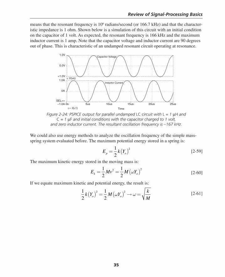
Review of Signal-Processing Basics
35
means that the resonant frequency is 106 radians/second (or 166.7 kHz) and that the character-istic impedance is 1 ohm. Shown below is a simulation of this circuit with an initial condition on the capacitor of 1 volt. As expected, the resonant frequency is 166 kHz and the maximum inductor current is 1 amp. Note that the capacitor voltage and inductor current are 90 degrees out of phase. This is characteristic of an undamped resonant circuit operating at resonance.
Figure 2-24: PSPICE output for parallel undamped LC circuit with L = 1 μH and C = 1 μF and initial conditions with the capacitor charged to 1 volt,
and zero inductor current. The resultant oscillation frequency is ∼167 kHz.
We could also use energy methods to analyze the oscillation frequency of the simple mass-spring system evaluated before. The maximum potential energy stored in a spring is:
E k Yp o= ( )1
2
2 [2-59]
The maximum kinetic energy stored in the moving mass is:
E Mv M Yk o= = ( )1
2
1
22 2
ω [2-60]
If we equate maximum kinetic and potential energy, the result is:
1
2
1
2
2 2k Y M Y
k
Mo o( ) = ( ) → =ω ω [2-61]
1.0V
0.0V
=1.0V
Time
Capacitor Voltage
Inductor Current
0s 5us 10us 15us 20us 25us�− I(L1)
� V(vc)1.0A
0A
SEL>>−1.0A
Thompson Book.indb 35 3/20/2006 11:33:47 AM

Chapter 2
36
Transfer Functions, Pole/Zero Plots and Bode PlotsShown in Table 2-2 are numerous transfer functions, their corresponding pole/zero plots and Bode frequency response plots.
Table 2-2: Transfer functions with their pole/zero and Bode frequency response plots.
System Type Transfer Function H(s) Pole/Zero Plot Bode Plot
Single Pole 1
1τ ps +
σ
ωj
x
τP– 1 ∠H(jω) τP
1ω
ω
1
0
–45
–90
⏐H(jω)⏐
Zero τzs +1
σ
ωj
o
τZ– 1 ∠H(jω) τZ
1ω
ω
1
+90
+45
0
⏐H(jω)⏐
Lead ττ
τ τz
pz p
s
s
++
>( )1
1,
σ
ωj
o
τZ– 1
x
τP– 1 ∠H(jω) τP
1τZ
1ω
ω
+90
+45
0
⏐H(jω)⏐
Lag ττ
τ τz
pz p
s
s
++
<( )1
1,
σ
ωj
x
τP– 1
o
τZ– 1 ∠H(jω)
ω
ω
0
–45
–90
⏐H(jω)⏐
Thompson Book.indb 36 3/20/2006 11:33:48 AM
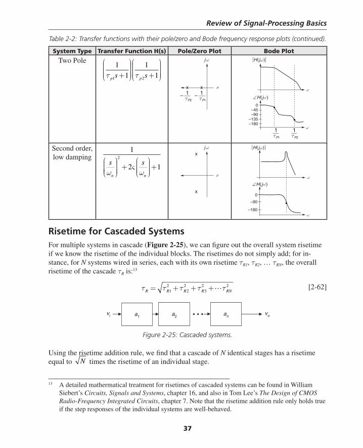
Review of Signal-Processing Basics
37
System Type Transfer Function H(s) Pole/Zero Plot Bode Plot
Two Pole1
1
1
11 2τ τp ps s+
⎛
⎝⎜⎜⎜⎜
⎞
⎠
⎟⎟⎟⎟⎟ +
⎛
⎝⎜⎜⎜⎜
⎞
⎠
⎟⎟⎟⎟⎟
σ
ωj
x
τP1– 1
x
τP2– 1
∠H(jω)
ω
ω
0–45–90
–135–180
⏐H(jω)⏐
τP2
1τP1
1
Second order, low damping
1
2 12
s s
n nω ω
⎛
⎝⎜⎜⎜⎜
⎞
⎠⎟⎟⎟⎟
+⎛
⎝⎜⎜⎜⎜
⎞
⎠⎟⎟⎟⎟+ς
σ
ωjx
x
∠H(jω)
ω
ω
0
–90
–180
⏐H(jω)⏐
Risetime for Cascaded SystemsFor multiple systems in cascade (Figure 2-25), we can fi gure out the overall system risetime if we know the risetime of the individual blocks. The risetimes do not simply add; for in-stance, for N systems wired in series, each with its own risetime τR1, τR2, … τRN, the overall risetime of the cascade τR is:13
τ τ τ τ τR R R R RN= + + +12
22
32 2 [2-62]
a1vi voa2 an
Figure 2-25: Cascaded systems.
Using the risetime addition rule, we fi nd that a cascade of N identical stages has a risetime equal to N times the risetime of an individual stage.
13 A detailed mathermatical treatment for risetimes of cascaded systems can be found in William Siebert’s Circuits, Signals and Systems, chapter 16, and also in Tom Lee’s The Design of CMOS Radio-Frequency Integrated Circuits, chapter 7. Note that the risetime addition rule only holds true if the step responses of the individual systems are well-behaved.
Table 2-2: Transfer functions with their pole/zero and Bode frequency response plots (continued).
Thompson Book.indb 37 3/20/2006 11:33:49 AM

38
Chapter 2 Problems
Problem 2.1A single-pole low-pass fi lter (Figure 2-26) has R = 1 kΩ and C = 1000 pF. Find the input-output transfer function H(s) and calculate the 10–90% risetime and –3dB bandwidth of this circuit.
Problem 2.2Find and plot the angle and group delay of the single pole fi lter of Problem 2.1.
Problem 2.3Simulate the circuit of Problem 2.1 and verify your results in Problems 2.1 and 2.2.
Problem 2.4Design a second-order RLC circuit with an input-output transfer function exhibiting a natural frequency ωn = 106 radians/second and a damping ratio ζ = 0.1. What is the Q of this circuit ?
Problem 2.5For the circuit of Problem 2.4, plot the magnitude and angle of the transfer function. Correlate the simulated peak in the magnitude response with circuit Q.
Problem 2.6A mass-spring system has mass M = 10 kg and spring constant k = 10 Newtons/meter. What is the oscillation frequency of this system?
Problem 2.7An undamped parallel resonant circuit has L = 10 microhenries and C = 100 microfarads. At time t = 0, the capacitor is charged to 1V and the inductor current is zero. Find and plot capacitor voltage and inductor current for t > 0. What is the peak inductor current?
C
Rvo
vi
1000 pF
1k
Figure 2-26: Single-pole fi lter
Thompson Book.indb 38 3/20/2006 11:33:50 AM
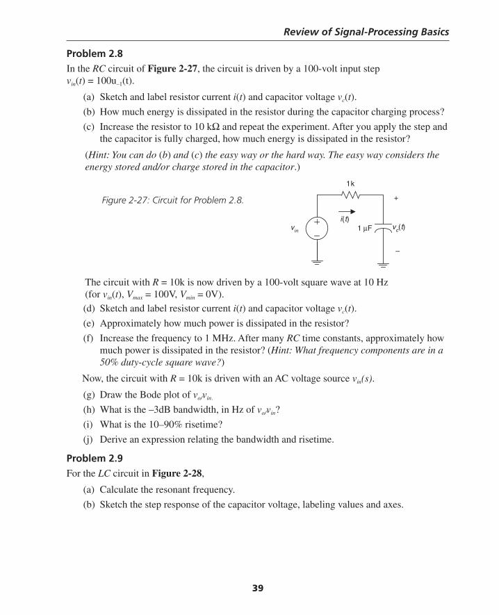
Review of Signal-Processing Basics
39
Problem 2.8In the RC circuit of Figure 2-27, the circuit is driven by a 100-volt input step vin(t) = 100u–1(t).
(a) Sketch and label resistor current i(t) and capacitor voltage vc(t).
(b) How much energy is dissipated in the resistor during the capacitor charging process?
(c) Increase the resistor to 10 kΩ and repeat the experiment. After you apply the step and the capacitor is fully charged, how much energy is dissipated in the resistor?
(Hint: You can do (b) and (c) the easy way or the hard way. The easy way considers the energy stored and/or charge stored in the capacitor.)
1k
1 μFvin
i(t)
+
–
vc(t)
Figure 2-27: Circuit for Problem 2.8.
The circuit with R = 10k is now driven by a 100-volt square wave at 10 Hz (for vin(t), Vmax = 100V, Vmin = 0V).(d) Sketch and label resistor current i(t) and capacitor voltage vc(t).
(e) Approximately how much power is dissipated in the resistor?
(f) Increase the frequency to 1 MHz. After many RC time constants, approximately how much power is dissipated in the resistor? (Hint: What frequency components are in a 50% duty-cycle square wave?)
Now, the circuit with R = 10k is driven with an AC voltage source vin(s).
(g) Draw the Bode plot of vo/vin.
(h) What is the –3dB bandwidth, in Hz of vo/vin?
(i) What is the 10–90% risetime?
(j) Derive an expression relating the bandwidth and risetime.
Problem 2.9 For the LC circuit in Figure 2-28,
(a) Calculate the resonant frequency.
(b) Sketch the step response of the capacitor voltage, labeling values and axes.
Thompson Book.indb 39 3/20/2006 11:33:51 AM
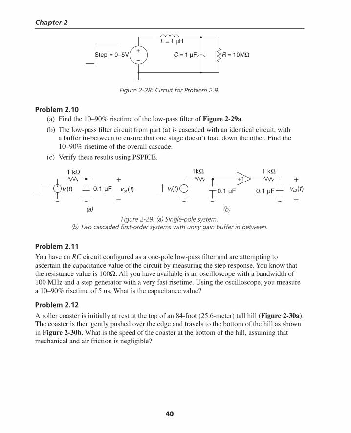
Chapter 2
40
Figure 2-28: Circuit for Problem 2.9.
Problem 2.10(a) Find the 10–90% risetime of the low-pass fi lter of Figure 2-29a.
(b) The low-pass fi lter circuit from part (a) is cascaded with an identical circuit, with a buffer in-between to ensure that one stage doesn’t load down the other. Find the 10–90% risetime of the overall cascade.
(c) Verify these results using PSPICE.
R = 10MΩ
L = 1 µH
C = 1 µFStep = 0–5V+
−
vi(t)
1 kΩ
vo1(t)0.1 µF
+
–
+
–vi(t) vo2(t)
1kΩ 1 kΩ
0.1 µF 0.1 µF
+1
(a) (b)
Figure 2-29: (a) Single-pole system. (b) Two cascaded fi rst-order systems with unity gain buffer in between.
Problem 2.11You have an RC circuit confi gured as a one-pole low-pass fi lter and are attempting to ascertain the capacitance value of the circuit by measuring the step response. You know that the resistance value is 100Ω. All you have available is an oscilloscope with a bandwidth of 100 MHz and a step generator with a very fast risetime. Using the oscilloscope, you measure a 10–90% risetime of 5 ns. What is the capacitance value?
Problem 2.12A roller coaster is initially at rest at the top of an 84-foot (25.6-meter) tall hill (Figure 2-30a). The coaster is then gently pushed over the edge and travels to the bottom of the hill as shown in Figure 2-30b. What is the speed of the coaster at the bottom of the hill, assuming that mechanical and air friction is negligible?
Thompson Book.indb 40 3/20/2006 11:33:51 AM
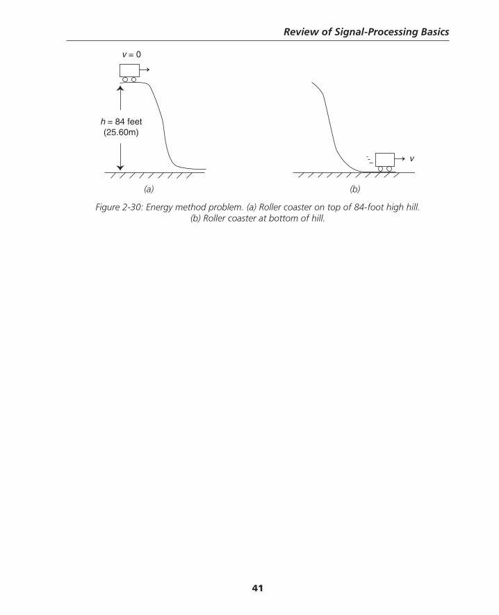
Review of Signal-Processing Basics
41
(a) (b)
Figure 2-30: Energy method problem. (a) Roller coaster on top of 84-foot high hill. (b) Roller coaster at bottom of hill.
v = 0
v
h = 84 feet(25.60m)
Thompson Book.indb 41 3/20/2006 11:33:52 AM
Chapter 2
42
ReferencesAndrews, James, “Low-Pass Risetime Filters for Time Domain Applications,” Picosecond
Pulse Labs, Application note #AN-7a, 1999.Beranek, Leo L., Acoustics, Acoustical Society of America, 1954.CRC Press, CRC Standard Mathematical Tables, 28th edition, 1987.Guillemin, Ernst, Introductory Circuit Theory, John Wiley, 1953.Johnson, Howard, “Risetime of Lossy Transmission Lines,” EDN, October 2, 2003, p. 32.Lee, Thomas H., The Design of CMOS Radio-Frequency Integrated Circuits.Rao, Singiresu S., Mechanical Vibrations, 3rd edition, Addison-Wesley, 1995.Roberge, James, Operational Amplifi ers: Theory and Practice, John Wiley, 1975.Senturia, Stephen D., and Wedlock, Bruce D., Electronic Circuits and Applications, reprinted
by Krieger, 1993.Siebert, William McC., Circuits, Signals and Systems, McGraw-Hill, 1986.
Thompson Book.indb 42 3/20/2006 11:33:52 AM
43
C H A P T E R 3Review of Diode Physics and the Ideal (and Later, Nonideal) Diode
Current Flow in Insulators, Good Conductors and SemiconductorsIn nature, from the point of view of the ease of producing current fl ow in a material, there are three broad classes of materials: insulators, conductors and semiconductors. Semiconductors and metals can support signifi cant current fl ow but the charge movement mechanisms are dif-ferent in the two types of materials. How “good” an electrical conductor is can be quantifi ed by material property electrical resistivity and/or its inverse, electrical conductivity. Electrical resistivity2 is a measure of how well a given material conducts current. If there are lots of free charged carriers available, a material is deemed a good conductor.
In This Chapter
The basics of bipolar devices are covered, including basic semiconductor physics ,1 the concepts of electron and hole fl ow in semiconductors, the differences between drift and diffusion fl ow, generation and recombination, and the effects of semiconductor doping on carrier concentrations. We fi nish with a discussion of the ideal diode, and illustrate how a diode can conduct forward current, but can also block reverse voltage. Detailed mathematical derivations are avoided wherever possible. However, enough mathematical detail is given so that the reader can discern the important scaling laws and functional dependencies of the ideal diode. At the end of the chapter we’ll discuss some of the factors that result in nonideal behavior in diodes. We’ll conclude with a discussion of load lines, a useful method for solving for the operating point of circuits with nonlinear devices. The load-line technique will be useful in later chapters in analyzing transistors.
1 We will not go into the quantum mechanics of semiconductors, which provides the rigorous analyses. The simpler models developed in this chapter hopefully will give insight into the basics of semiconductor operation. Excellent reviews of semiconductor physics are given in Shockley’s and Bardeen’s 1956 Nobel prize lectures, with reference given at the end of this chapter.
2 If you look in technical references (such as the Handbook of Chemistry and Physics) you can often fi nd electrical conductivity listed for materials. Electrical resistivity has units of ohms-meters. Electrical conductivity is the inverse of electrical resistivity.
Thompson Book.indb 43 3/20/2006 11:33:52 AM
Chapter 3
44
Insulators are materials such as quartz, rubber, plastics and certain ceramics which do not support current fl ow very well. In other words, the electrical resistivity of an insulating mate-rial is very high. The resistance to current fl ow is very high in insulators because there are very few free charges available to contribute to current fl ow.
Good conductors support current fl ow easily. In other words, to get substantial current fl ow in a good conductor you don’t have to supply very much driving voltage. Some metals, such as copper, aluminum, gold and silver, are very good conductors because they have a sea of free electrons, each with a negative charge –q associated with them,3 available to support current fl ow. Typical metals have electrical conductivity many orders of magnitude higher than semi-conductors or insulators. Most metals are good conductors; however, none of them are perfect conductors,4 at least at room temperature.
Let’s do a simple calculation of the resistance of a copper rod (Figure 3-1). The electrical resistance of the rod5 is:
l
RAσ
= [3-1]
where l is the length, A is cross-sectional area and σ is electrical conductivity (which has units of Ω–1m–1). Let’s connect a battery to the metal rod as shown in Figure 3-1. The current fl ow is left to right in the metal rod (corresponding to electron fl ow from right to left6). For a metal rod of length 0.1 meters and cross-sectional area 10–4 m2, the resistance at room temperature7 is approximately 16.9 microohms.
3 The charge on an electron is –q, where q ≈ 1.6 × 10⁻¹⁹ Coulombs.4 There are compounds, such as niobium-titanium, which become superconducting at cryogenic
temperatures (e.g., liquid helium temperature, at 4.2K). Scientists are searching for super-conductors (conductors whose electrical resistivity goes to zero if the temperature is lowered below a critical temperature). As of yet, no room-temperature superconductors have been discovered. The electrical conductivity of copper at room temperature is approximately 5.9 × 10⁷ Ω–1m–1, while that of aluminum is approximately 3.5 × 10⁷ Ω–1m–1. Note that these values of electrical conductivity vary signifi cantly with the specifi c alloy, and that electrical conductivity of metals increases as operating temperature decreases.
5 This calculation ignores any resistance due to contacts at the ends of the rod.6 Note that the charge on the electron is negative. Hence, when electrons fl ow from right to left, the
net current fl ow is from left to right. The directions of current fl ow are shown by convention.7 Electrical resistivity is the inverse of electrical conductivity. The electrical resistivity of copper at
room temperature is approximately 1.7 × 10⁻⁸ Ω-m. The temperature coeffi cient of resistivity of copper is approximately +0.4% per degree C.
Thompson Book.indb 44 3/20/2006 11:33:53 AM
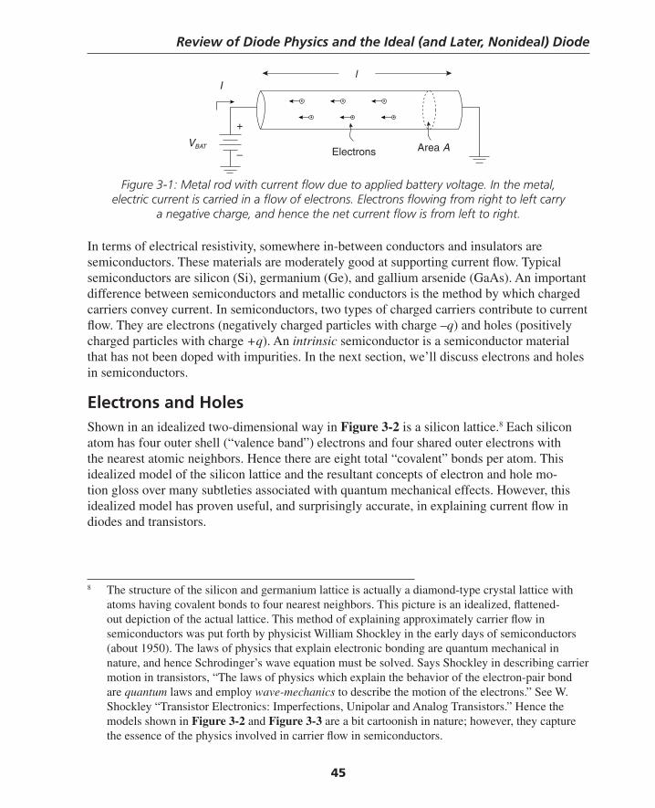
Review of Diode Physics and the Ideal (and Later, Nonideal) Diode
45
Figure 3-1: Metal rod with current fl ow due to applied battery voltage. In the metal, electric current is carried in a fl ow of electrons. Electrons fl owing from right to left carry
a negative charge, and hence the net current fl ow is from left to right.
In terms of electrical resistivity, somewhere in-between conductors and insulators are semiconductors. These materials are moderately good at supporting current fl ow. Typical semiconductors are silicon (Si), germanium (Ge), and gallium arsenide (GaAs). An important difference between semiconductors and metallic conductors is the method by which charged carriers convey current. In semiconductors, two types of charged carriers contribute to current fl ow. They are electrons (negatively charged particles with charge –q) and holes (positively charged particles with charge +q). An intrinsic semiconductor is a semiconductor material that has not been doped with impurities. In the next section, we’ll discuss electrons and holes in semiconductors.
Electrons and HolesShown in an idealized two-dimensional way in Figure 3-2 is a silicon lattice.8 Each silicon atom has four outer shell (“valence band”) electrons and four shared outer electrons with the nearest atomic neighbors. Hence there are eight total “covalent” bonds per atom. This idealized model of the silicon lattice and the resultant concepts of electron and hole mo-tion gloss over many subtleties associated with quantum mechanical effects. However, this idealized model has proven useful, and surprisingly accurate, in explaining current fl ow in diodes and transistors.
lI
VBATElectrons Area A
+
–
8 The structure of the silicon and germanium lattice is actually a diamond-type crystal lattice with atoms having covalent bonds to four nearest neighbors. This picture is an idealized, fl attened-out depiction of the actual lattice. This method of explaining approximately carrier fl ow in semiconductors was put forth by physicist William Shockley in the early days of semiconductors (about 1950). The laws of physics that explain electronic bonding are quantum mechanical in nature, and hence Schrodinger’s wave equation must be solved. Says Shockley in describing carrier motion in transistors, “The laws of physics which explain the behavior of the electron-pair bond are quantum laws and employ wave-mechanics to describe the motion of the electrons.” See W. Shockley “Transistor Electronics: Imperfections, Unipolar and Analog Transistors.” Hence the models shown in Figure 3-2 and Figure 3-3 are a bit cartoonish in nature; however, they capture the essence of the physics involved in carrier fl ow in semiconductors.
Thompson Book.indb 45 3/20/2006 11:33:54 AM

Chapter 3
46
In the ideal lattice, all of the covalent bonds are fi lled and the associated electrons are tightly bound to their neighboring nuclei. Therefore, no “free” charges are available to contribute to current fl ow. 9
9 This is how a semiconductor behaves at very low temperatures. At cryogenic temperatures, for example, few outer shell bonds are broken (since the lattice is so cold and there is not enough thermal energy to shake electrons free).
10 It’s simple to fi nd the total current in a semiconductor if you can calculate the current density J. Just multiply current density J (with units of amps/m2) by the total cross-sectional area A through which the current fl ows: I = JA.
Now, in a real-world semiconductor, some fraction of these covalent bonds break due to the random thermal energy of the silicon lattice (Figure 3-3). If a voltage is applied to the sample, these free electrons can fl ow and support a net current. The resultant space where the electron was before the bond was broken is called a hole. A hole carries a net positive charge of +q, and holes can also move about in the silicon lattice. In other words, the hole behaves like a charge carrier much like the electron, except that the hole carries a positive charge. The total current fl ow in a semiconductor is hence a combination of the current due to free elec-trons and the current due to free holes, or:
e hJ J J= + [3-2]
where J is total current density (expressed as amps per square meter10) and Je and Jh are the electron and hole currents, respectively.
Nucleus
Sharedcovalent
bond
Figure 3-2: Structure of idealized silicon lattice with all covalent bonds fi lled.
+
+
–
Freeelectron
–
Figure 3-3: Real-world silicon lattice with some broken covalent bonds.
Each broken bond allows a negatively charged electron and a positively
charged hole to move.
Thompson Book.indb 46 3/20/2006 11:33:55 AM
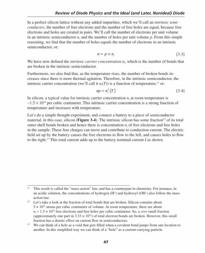
Review of Diode Physics and the Ideal (and Later, Nonideal) Diode
47
In a perfect silicon lattice without any added impurities, which we’ll call an intrinsic semi-conductor, the number of free electrons and the number of free holes are equal, because free electrons and holes are created in pairs. We’ll call the number of electrons per unit volume in an intrinsic semiconductor n, and the number of holes per unit volume p. From this simple reasoning, we fi nd that the number of holes equals the number of electrons in an intrinsic semiconductor, or:
in p n= ≡ [3-3]
We have now defi ned the intrinsic carrier concentration ni, which is the number of bonds that are broken in the intrinsic semiconductor.
Furthermore, we also fi nd that, as the temperature rises, the number of broken bonds in-creases since there is more thermal agitation. Therefore, in the intrinsic semiconductor, the intrinsic carrier concentration (we’ll call it ni(T)) is a function of temperature,11 or:
( )2inp n T= [3-4]
In silicon, a typical value for intrinsic carrier concentration ni at room temperature is ∼1.5 × 10¹⁰ per cubic centimeter. This intrinsic carrier concentration is a strong function of temperature and increases with temperature.
Let’s do a simple thought experiment, and connect a battery to a piece of semiconductor material, in this case, silicon (Figure 3-4). The intrinsic silicon has some fraction12 of its total outer-shell bonds broken and hence there is concentration ni of free electrons and free holes in the sample. These free charges can move and contribute to conduction current. The electric fi eld set up by the battery causes the free electrons to fl ow to the left, and causes holes to fl ow to the right.13 This total current adds up to the battery terminal current I as shown.
11 This result is called the “mass-action” law, and has a counterpart in chemistry. For instance, in an acidic solution, the concentrations of hydrogen (H+) and hydroxyl (OH–) also follow the mass action law.
12 Let’s take a look at the fraction of total bonds that are broken. Silicon contains about 5 × 10²² atoms per cubic centimeter of volume. At room temperature, there are about ni ≈ 1.5 × 10¹⁰ free electrons and free holes per cubic centimeter. So, a very small fraction (approximately one part in 3.33 × 10¹²) of total electron bonds are broken. However, this small fraction has a drastic effect on current fl ow in semiconductors.
13 We can think of a hole as a void that gets fi lled when a covalent bond jumps from one location to another. In this simplifi ed way we can think of a “hole” as a current-carrying particle.
Thompson Book.indb 47 3/20/2006 11:33:55 AM
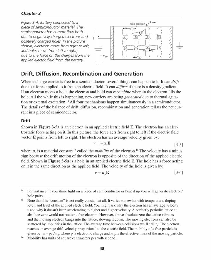
Chapter 3
48
14 For instance, if you shine light on a piece of semiconductor or heat it up you will generate electron/hole pairs.
15 Note that this “constant” is not really constant at all. It varies somewhat with temperature, doping level, and level of the applied electric fi eld. You might ask why the electron has an average velocity v and why it doesn’t keep accelerating to higher and higher velocity. A perfectly periodic lattice at absolute zero would not scatter a free electron. However, above absolute zero the lattice vibrates and the moving electron bangs into the lattice, slowing it down. The moving electrons can also be scattered by impurities in the lattice. The average time between collisions we’ll call τc. The electron reaches an average drift velocity proportional to the electric fi eld. The mobility of a free particle is given by: μ = qτc/meff where q is electronic charge and meff is the effective mass of the moving particle.
16 Mobility has units of square centimeters per volt-second.
Drift, Diffusion, Recombination and GenerationWhen a charge carrier is free in a semiconductor, several things can happen to it. It can drift due to a force applied to it from an electric fi eld. It can diffuse if there is a density gradient. If an electron meets a hole, the electron and hold can recombine wherein the electron fi lls the hole. All the while this is happening, new carriers are being generated due to thermal agita-tion or external excitation.14 All four mechanisms happen simultaneously in a semiconductor. The details of the balance of drift, diffusion, recombination and generation tell us the net cur-rent in a piece of semiconductor.
DriftShown in Figure 3-5a is an electron in an applied electric fi eld E. The electron has an elec-trostatic force acting on it. In this picture, the force acts from right to left if the electric fi eld vector E points from left to right. The electron has an average velocity given by:
nv μ= − E [3-5]
where µn is a material constant15 called the mobility of the electron.16 The velocity has a minus sign because the drift motion of the electron is opposite of the direction of the applied electric fi eld. Shown in Figure 3-5a is a hole in an applied electric fi eld E. The hole has a force acting on it in the same direction as the applied fi eld. The velocity of the hole is given by:
pv μ= E [3-6]
I
VBAT
+
–
Free electron
–
–
+
+Si Si Si Si
Si Si Si Si
HoleFigure 3-4: Battery connected to a piece of semiconductor material. The semiconductor has current fl ow both due to negatively charged electrons and positively charged holes. In the picture shown, electrons move from right to left, and holes move from left to right, due to the force on the charges from the applied electric fi eld from the battery.
Thompson Book.indb 48 3/20/2006 11:33:56 AM
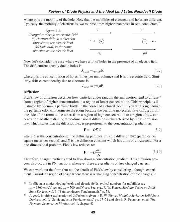
Review of Diode Physics and the Ideal (and Later, Nonideal) Diode
49
where µp is the mobility of the hole. Note that the mobilities of electrons and holes are different. Typically, the mobility of electrons is two to three times higher than holes in semiconductors.17
17 In silicon at modest doping levels and electric fi elds, typical numbers for mobilities are μn ≈ 1360 cm2/V-sec and μp ≈ 500 cm2/V-sec. See, e.g., R. W. Pierret, Modular Series on Solid State Devices, vol. 1, “Semiconductor Fundamentals,” p. 58.
18 A good, intuitive explanation of diffusion is given in R. W. Pierret, Modular Series on Solid State Devices, vol. 1, “Semiconductor Fundamentals,” pp. 67–71 and also in R. Feynman, et. al, The Feynman Lectures on Physics, vol. 1, chapter 43.
Now, let’s consider the case where we have a lot of holes in the presence of an electric fi eld. The drift current density due to holes is:
,h drift pJ q pμ= E [3-7]
where p is the concentration of holes (holes per unit volume) and E is the electric fi eld. Simi-larly, drift current density due to electrons is:
,n drift nJ q nμ= E [3-8]
DiffusionFick’s law of diffusion describes how particles under random thermal motion tend to diffuse18 from a region of higher concentration to a region of lower concentration. This principle is il-lustrated by opening a perfume bottle in the corner of a closed room. If you wait long enough, the perfume odor will permeate the room because the perfume molecules have diffused from one side of the room to the other, from a region of high concentration to a region of low con-centration. Mathematically, three-dimensional diffusion is characterized by Fick’s diffusion law, which states that the diffusion fl ux is proportional to the concentration gradient, as:
D C= − ∇F [3-9]
where C is the concentration of the diffusing particles, F is the diffusion fl ux (particles per square meter per second) and D is the diffusion constant which has units of cm2/second. For a one-dimensional problem, Fick’s law reduces to:
dCD
dx= −F [3-10]
Therefore, charged particles tend to fl ow down a concentration gradient. This diffusion pro-cess also occurs in PN junctions whenever there are gradients of free charged carriers.
We can work out the form (but not the detail) of Fick’s law by considering a thought experi-ment. Consider a region of space where there is a changing concentration of free charges, in
–
E
v +
E
v
Figure 3-5: Charged carriers in an electric fi eld.
(a) Electron drift, in a direction opposite to the electric fi eld.
(b) Hole drift, in the same direction as the electric fi eld.
(a) (b)
Thompson Book.indb 49 3/20/2006 11:33:56 AM
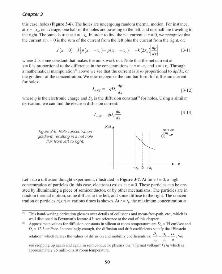
Chapter 3
50
this case, holes (Figure 3-6). The holes are undergoing random thermal motion. For instance, at x = –xo, on average, one half of the holes are traveling to the left, and one half are traveling to the right. The same is true at x = +xo. In order to fi nd the net current at x = 0, we recognize that the current at x = 0 is the sum of the current from the left plus the current from the right, or:
( ) ( ) ( ) ( )0 2o o o
dpJ x k p x x p x x k x
dx
⎡ ⎤⎡ ⎤ ⎢ ⎥= = = − − = + = −⎣ ⎦ ⎢ ⎥⎣ ⎦ [3-11]
where k is some constant that makes the units work out. Note that the net current at x = 0 is proportional to the difference in the concentrations at x = –xo and x = +xo. Through a mathematical manipulation19 above we see that the current is also proportional to dp/dx, or the gradient of the concentration. We now recognize the familiar form for diffusion current for holes:
,h diff p
dpJ qD
dx= − [3-12]
where q is the electronic charge and Dp is the diffusion constant20 for holes. Using a similar derivation, we can fi nd the electron diffusion current:
,e diff n
dnJ qD
dx= [3-13]
x+x00–x0
p(x)Net HoleFlux+
Figure 3-6: Hole concentration gradient, resulting in a net hole
fl ux from left to right.
19 This hand-waving derivation glosses over details of collisions and mean-free-path, etc., which is well discussed in Feynman’s lecture 43; see reference at the end of this chapter.
20 Approximate values for diffusion constants in silicon at room temperature are Dn ≈ 35 cm2/sec and Dp ≈ 12.5 cm2/sec. Interestingly enough, the diffusion and drift coeffi cients satisfy the “Einstein
relation” which relates the values of diffusion and mobility coeffi cients as: D D kT
qp
p
n
nμ μ= = . We
see cropping up again and again in semiconductor physics the “thermal voltage” kT/q which is approximately 26 millivolts at room temperature.
Let’s do a diffusion thought experiment, illustrated in Figure 3-7. At time t = 0, a high concentration of particles (in this case, electrons) exists at x = 0. These particles can be cre-ated by illuminating a piece of semiconductor, or by other mechanisms. The particles are in random thermal motion; some diffuse to the left, and some diffuse to the right. The concen-tration of particles n(x,t) at various times is shown. At t = t1, the maximum concentration at
Thompson Book.indb 50 3/20/2006 11:33:57 AM
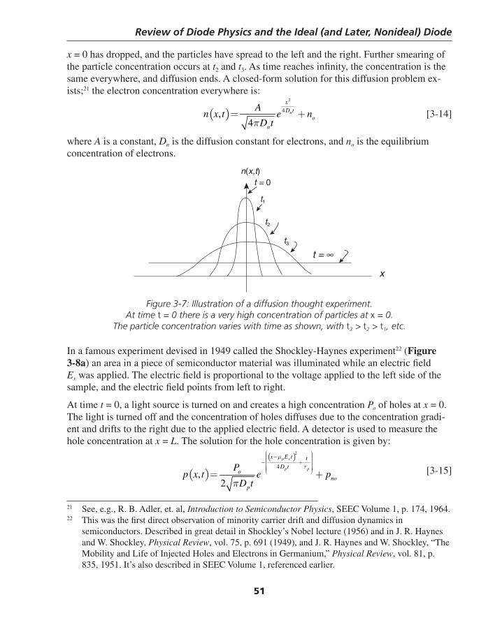
Review of Diode Physics and the Ideal (and Later, Nonideal) Diode
51
x = 0 has dropped, and the particles have spread to the left and the right. Further smearing of the particle concentration occurs at t2 and t3. As time reaches infi nity, the concentration is the same everywhere, and diffusion ends. A closed-form solution for this diffusion problem ex-ists;21 the electron concentration everywhere is:
( )2
4,4
n
x
D to
n
An x t e n
D tπ= + [3-14]
where A is a constant, Dn is the diffusion constant for electrons, and no is the equilibrium concentration of electrons.
Figure 3-7: Illustration of a diffusion thought experiment. At time t = 0 there is a very high concentration of particles at x = 0.
The particle concentration varies with time as shown, with t3 > t2 > t1, etc.
In a famous experiment devised in 1949 called the Shockley-Haynes experiment22 (Figure 3-8a) an area in a piece of semiconductor material was illuminated while an electric fi eld Ex was applied. The electric fi eld is proportional to the voltage applied to the left side of the sample, and the electric fi eld points from left to right.
At time t = 0, a light source is turned on and creates a high concentration Po of holes at x = 0. The light is turned off and the concentration of holes diffuses due to the concentration gradi-ent and drifts to the right due to the applied electric fi eld. A detector is used to measure the hole concentration at x = L. The solution for the hole concentration is given by:
( )( )2
4
,2
p x
p p
x E t t
D to
no
p
Pp x t e p
D t
μ
τ
π
⎛ ⎞⎟⎜ − ⎟⎜ ⎟⎜ ⎟− +⎜ ⎟⎜ ⎟⎜ ⎟⎟⎜ ⎟⎜⎝ ⎠= + [3-15]
21 See, e.g., R. B. Adler, et. al, Introduction to Semiconductor Physics, SEEC Volume 1, p. 174, 1964.22 This was the fi rst direct observation of minority carrier drift and diffusion dynamics in
semiconductors. Described in great detail in Shockley’s Nobel lecture (1956) and in J. R. Haynes and W. Shockley, Physical Review, vol. 75, p. 691 (1949), and J. R. Haynes and W. Shockley, “The Mobility and Life of Injected Holes and Electrons in Germanium,” Physical Review, vol. 81, p. 835, 1951. It’s also described in SEEC Volume 1, referenced earlier.
x
t = ∞
n(x,t)t = 0
t1
t2
t3
Thompson Book.indb 51 3/20/2006 11:33:58 AM
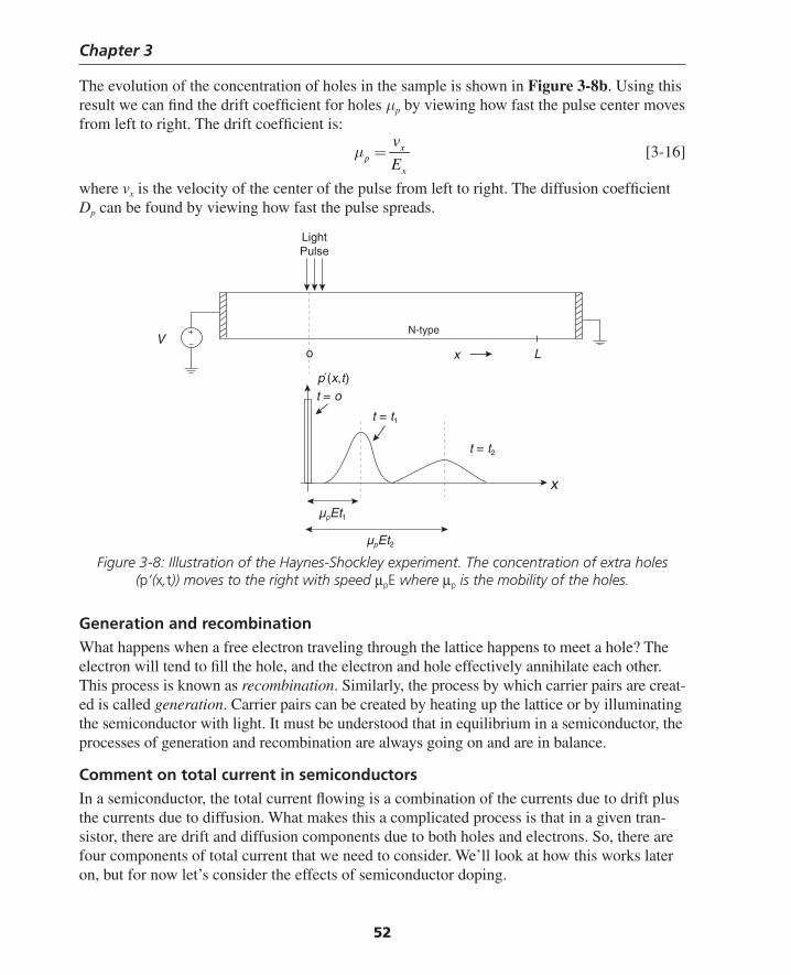
Chapter 3
52
The evolution of the concentration of holes in the sample is shown in Figure 3-8b. Using this result we can fi nd the drift coeffi cient for holes μp by viewing how fast the pulse center moves from left to right. The drift coeffi cient is:
xp
x
v
Eμ = [3-16]
where vx is the velocity of the center of the pulse from left to right. The diffusion coeffi cient Dp can be found by viewing how fast the pulse spreads.
V
LightPulse
x Lo
N-type
p (x,t)t = o
t = t1
t = t2
x
µpEt1
µpEt2
Figure 3-8: Illustration of the Haynes-Shockley experiment. The concentration of extra holes (p’(x,t)) moves to the right with speed μpE where μp is the mobility of the holes.
Generation and recombinationWhat happens when a free electron traveling through the lattice happens to meet a hole? The electron will tend to fi ll the hole, and the electron and hole effectively annihilate each other. This process is known as recombination. Similarly, the process by which carrier pairs are creat-ed is called generation. Carrier pairs can be created by heating up the lattice or by illuminating the semiconductor with light. It must be understood that in equilibrium in a semiconductor, the processes of generation and recombination are always going on and are in balance.
Comment on total current in semiconductorsIn a semiconductor, the total current fl owing is a combination of the currents due to drift plus the currents due to diffusion. What makes this a complicated process is that in a given tran-sistor, there are drift and diffusion components due to both holes and electrons. So, there are four components of total current that we need to consider. We’ll look at how this works later on, but for now let’s consider the effects of semiconductor doping.
Thompson Book.indb 52 3/20/2006 11:33:58 AM
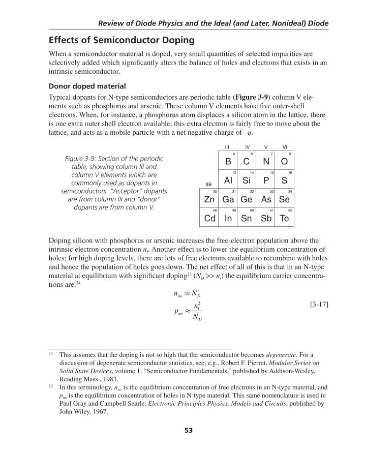
Review of Diode Physics and the Ideal (and Later, Nonideal) Diode
53
Effects of Semiconductor DopingWhen a semiconductor material is doped, very small quantities of selected impurities are selectively added which signifi cantly alters the balance of holes and electrons that exists in an intrinsic semiconductor.
Donor doped materialTypical dopants for N-type semiconductors are periodic table (Figure 3-9) column V ele-ments such as phosphorus and arsenic. These column V elements have fi ve outer-shell electrons. When, for instance, a phosphorus atom displaces a silicon atom in the lattice, there is one extra outer shell electron available; this extra electron is fairly free to move about the lattice, and acts as a mobile particle with a net negative charge of –q.
Doping silicon with phosphorus or arsenic increases the free-electron population above the intrinsic electron concentration ni. Another effect is to lower the equilibrium concentration of holes; for high doping levels, there are lots of free electrons available to recombine with holes and hence the population of holes goes down. The net effect of all of this is that in an N-type material at equilibrium with signifi cant doping23 (ND >> ni) the equilibrium carrier concentra-tions are:24
2
no D
ino
D
n N
np
N
≈
≈ [3-17]
III IV V VI
IIB
5 6 7 8
13 14 15 16
30 31 32 33 34
48 49 50 51 52
B C N O
AI Si P S
Zn Ga Ge As Se
Cd In Sn Sb Te
Figure 3-9: Section of the periodic table, showing column III and column V elements which are commonly used as dopants in
semiconductors. “Acceptor” dopants are from column III and “donor”
dopants are from column V.
23 This assumes that the doping is not so high that the semiconductor becomes degenerate. For a discussion of degenerate semiconductor statistics, see, e.g., Robert F. Pierret, Modular Series on Solid State Devices, volume 1, “Semiconductor Fundamentals,” published by Addison-Wesley, Reading Mass., 1983.
24 In this terminology, nno is the equilibrium concentration of free electrons in an N-type material, and pno is the equilibrium concentration of holes in N-type material. This same nomenclature is used in Paul Gray and Campbell Searle, Electronic Principles Physics, Models and Circuits, published by John Wiley, 1967.
Thompson Book.indb 53 3/20/2006 11:33:59 AM
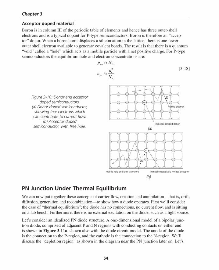
Chapter 3
54
mobile hole and later trajectory immobile negatively ionized acceptor
immobile ionized donor
–
+
B–
As+
mobile electron
Acceptor doped materialBoron is in column III of the periodic table of elements and hence has three outer-shell electrons and is a typical dopant for P-type semiconductors. Boron is therefore an “accep-tor” donor. When a boron atom displaces a silicon atom in the lattice, there is one fewer outer shell electron available to generate covalent bonds. The result is that there is a quantum “void” called a “hole” which acts as a mobile particle with a net positive charge. For P-type semiconductors the equilibrium hole and electron concentrations are:
2
po A
ipo
A
p N
nn
N
≈
≈ [3-18]
Figure 3-10: Donor and acceptor doped semiconductors.
(a) Donor doped semiconductor, showing free electrons which can contribute to current fl ow.
(b) Acceptor doped semiconductor, with free hole. (a)
(b)
PN Junction Under Thermal EquilibriumWe can now put together these concepts of carrier fl ow, creation and annihilation—that is, drift, diffusion, generation and recombination—to show how a diode operates. First we’ll consider the case of “thermal equilibrium”; the diode has no connections, no current fl ow, and is sitting on a lab bench. Furthermore, there is no external excitation on the diode, such as a light source.
Let’s consider an idealized PN diode structure. A one-dimensional model of a bipolar junc-tion diode, comprised of adjacent P and N regions with conducting contacts on either end is shown in Figure 3-11a, shown also with the diode circuit model. The anode of the diode is the connection to the P-region, and the cathode is the connection to the N-region. We’ll discuss the “depletion region” as shown in the diagram near the PN junction later on. Let’s
Thompson Book.indb 54 3/20/2006 11:33:59 AM
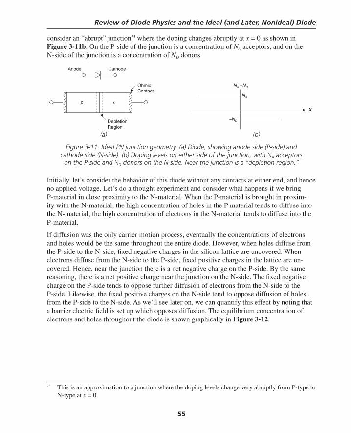
Review of Diode Physics and the Ideal (and Later, Nonideal) Diode
55
consider an “abrupt” junction25 where the doping changes abruptly at x = 0 as shown in Figure 3-11b. On the P-side of the junction is a concentration of NA acceptors, and on the N-side of the junction is a concentration of ND donors.
25 This is an approximation to a junction where the doping levels change very abruptly from P-type to N-type at x = 0.
(a) (b)
Figure 3-11: Ideal PN junction geometry. (a) Diode, showing anode side (P-side) and cathode side (N-side). (b) Doping levels on either side of the junction, with NA acceptors
on the P-side and ND donors on the N-side. Near the junction is a “depletion region.”
Initially, let’s consider the behavior of this diode without any contacts at either end, and hence no applied voltage. Let’s do a thought experiment and consider what happens if we bring P-material in close proximity to the N-material. When the P-material is brought in proxim-ity with the N-material, the high concentration of holes in the P material tends to diffuse into the N-material; the high concentration of electrons in the N-material tends to diffuse into the P-material.
If diffusion was the only carrier motion process, eventually the concentrations of electrons and holes would be the same throughout the entire diode. However, when holes diffuse from the P-side to the N-side, fi xed negative charges in the silicon lattice are uncovered. When electrons diffuse from the N-side to the P-side, fi xed positive charges in the lattice are un-covered. Hence, near the junction there is a net negative charge on the P-side. By the same reasoning, there is a net positive charge near the junction on the N-side. The fi xed negative charge on the P-side tends to oppose further diffusion of electrons from the N-side to the P-side. Likewise, the fi xed positive charges on the N-side tend to oppose diffusion of holes from the P-side to the N-side. As we’ll see later on, we can quantify this effect by noting that a barrier electric fi eld is set up which opposes diffusion. The equilibrium concentration of electrons and holes throughout the diode is shown graphically in Figure 3-12.
Anode Cathode
OhmicContact
DepletionRegion
p n
NA –ND
–ND
NA
x
Thompson Book.indb 55 3/20/2006 11:34:00 AM
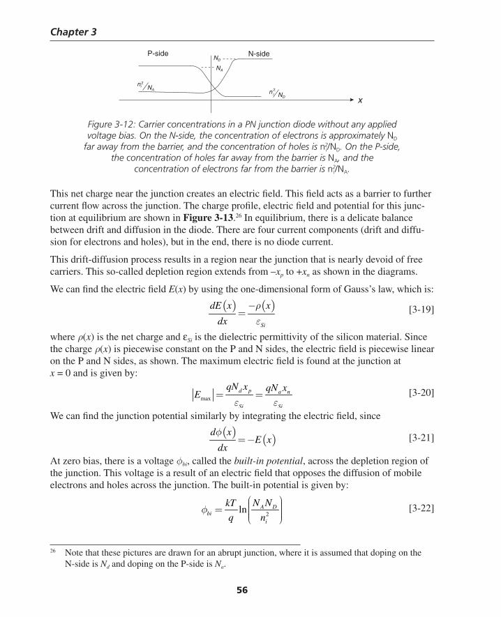
Chapter 3
56
Figure 3-12: Carrier concentrations in a PN junction diode without any applied voltage bias. On the N-side, the concentration of electrons is approximately ND
far away from the barrier, and the concentration of holes is ni2/ND. On the P-side,
the concentration of holes far away from the barrier is NA, and the concentration of electrons far from the barrier is ni
2/NA.
This net charge near the junction creates an electric fi eld. This fi eld acts as a barrier to further current fl ow across the junction. The charge profi le, electric fi eld and potential for this junc-tion at equilibrium are shown in Figure 3-13.26 In equilibrium, there is a delicate balance between drift and diffusion in the diode. There are four current components (drift and diffu-sion for electrons and holes), but in the end, there is no diode current.
This drift-diffusion process results in a region near the junction that is nearly devoid of free carriers. This so-called depletion region extends from –xp to +xn as shown in the diagrams.
We can fi nd the electric fi eld E(x) by using the one-dimensional form of Gauss’s law, which is:
( ) ( )Si
dE x x
dx
ρ
ε
−= [3-19]
where ρ(x) is the net charge and εSi is the dielectric permittivity of the silicon material. Since the charge ρ(x) is piecewise constant on the P and N sides, the electric fi eld is piecewise linear on the P and N sides, as shown. The maximum electric fi eld is found at the junction at x = 0 and is given by:
max
d p a n
Si Si
qN x qN xE
ε ε= = [3-20]
We can fi nd the junction potential similarly by integrating the electric fi eld, since
( )( )
d xE x
dx
φ= − [3-21]
At zero bias, there is a voltage φbi, called the built-in potential, across the depletion region of the junction. This voltage is a result of an electric fi eld that opposes the diffusion of mobile electrons and holes across the junction. The built-in potential is given by:
2
ln A Dbi
i
N NkT
q nφ
⎛ ⎞⎟⎜ ⎟= ⎜ ⎟⎜ ⎟⎜⎝ ⎠ [3-22]
26 Note that these pictures are drawn for an abrupt junction, where it is assumed that doping on the N-side is Nd and doping on the P-side is Na.
x
P-side N-sideND
NA
ND
NAni
2
n 2i
Thompson Book.indb 56 3/20/2006 11:34:00 AM
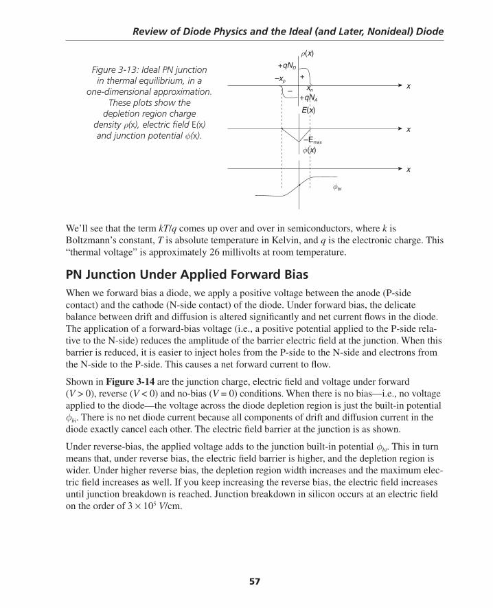
Review of Diode Physics and the Ideal (and Later, Nonideal) Diode
57
We’ll see that the term kT/q comes up over and over in semiconductors, where k is Boltzmann’s constant, T is absolute temperature in Kelvin, and q is the electronic charge. This “thermal voltage” is approximately 26 millivolts at room temperature.
PN Junction Under Applied Forward BiasWhen we forward bias a diode, we apply a positive voltage between the anode (P-side contact) and the cathode (N-side contact) of the diode. Under forward bias, the delicate balance between drift and diffusion is altered signifi cantly and net current fl ows in the diode. The application of a forward-bias voltage (i.e., a positive potential applied to the P-side rela-tive to the N-side) reduces the amplitude of the barrier electric fi eld at the junction. When this barrier is reduced, it is easier to inject holes from the P-side to the N-side and electrons from the N-side to the P-side. This causes a net forward current to fl ow.
Shown in Figure 3-14 are the junction charge, electric fi eld and voltage under forward (V > 0), reverse (V < 0) and no-bias (V = 0) conditions. When there is no bias—i.e., no voltage applied to the diode—the voltage across the diode depletion region is just the built-in potential φbi. There is no net diode current because all components of drift and diffusion current in the diode exactly cancel each other. The electric fi eld barrier at the junction is as shown.
Under reverse-bias, the applied voltage adds to the junction built-in potential φbi. This in turn means that, under reverse bias, the electric fi eld barrier is higher, and the depletion region is wider. Under higher reverse bias, the depletion region width increases and the maximum elec-tric fi eld increases as well. If you keep increasing the reverse bias, the electric fi eld increases until junction breakdown is reached. Junction breakdown in silicon occurs at an electric fi eld on the order of 3 × 10⁵ V/cm.
x
x
x
ρ(x)
+qND
+qNA
xn
–xp
E(x)
+
–
–Emax
φ(x)
φbi
Figure 3-13: Ideal PN junction in thermal equilibrium, in a
one-dimensional approximation. These plots show the
depletion region charge density ρ(x), electric fi eld E(x) and junction potential φ(x).
Thompson Book.indb 57 3/20/2006 11:34:01 AM
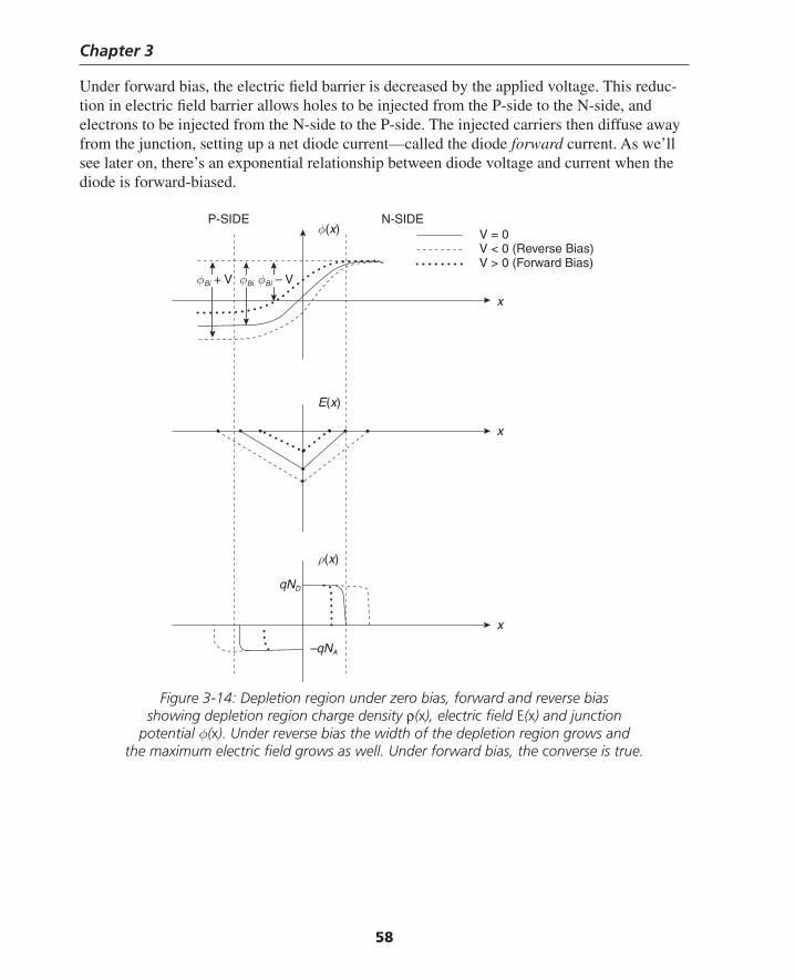
Chapter 3
58
Under forward bias, the electric fi eld barrier is decreased by the applied voltage. This reduc-tion in electric fi eld barrier allows holes to be injected from the P-side to the N-side, and electrons to be injected from the N-side to the P-side. The injected carriers then diffuse away from the junction, setting up a net diode current—called the diode forward current. As we’ll see later on, there’s an exponential relationship between diode voltage and current when the diode is forward-biased.
φ(x)P-SIDE N-SIDE
V = 0V < 0 (Reverse Bias)V > 0 (Forward Bias)
x
x
E(x)
x
ρ(x)
φBi + V φBi – VφBi
qND
–qNA
Figure 3-14: Depletion region under zero bias, forward and reverse bias showing depletion region charge density ρ(x), electric fi eld E(x) and junction
potential φ(x). Under reverse bias the width of the depletion region grows and the maximum electric fi eld grows as well. Under forward bias, the converse is true.
Thompson Book.indb 58 3/20/2006 11:34:01 AM
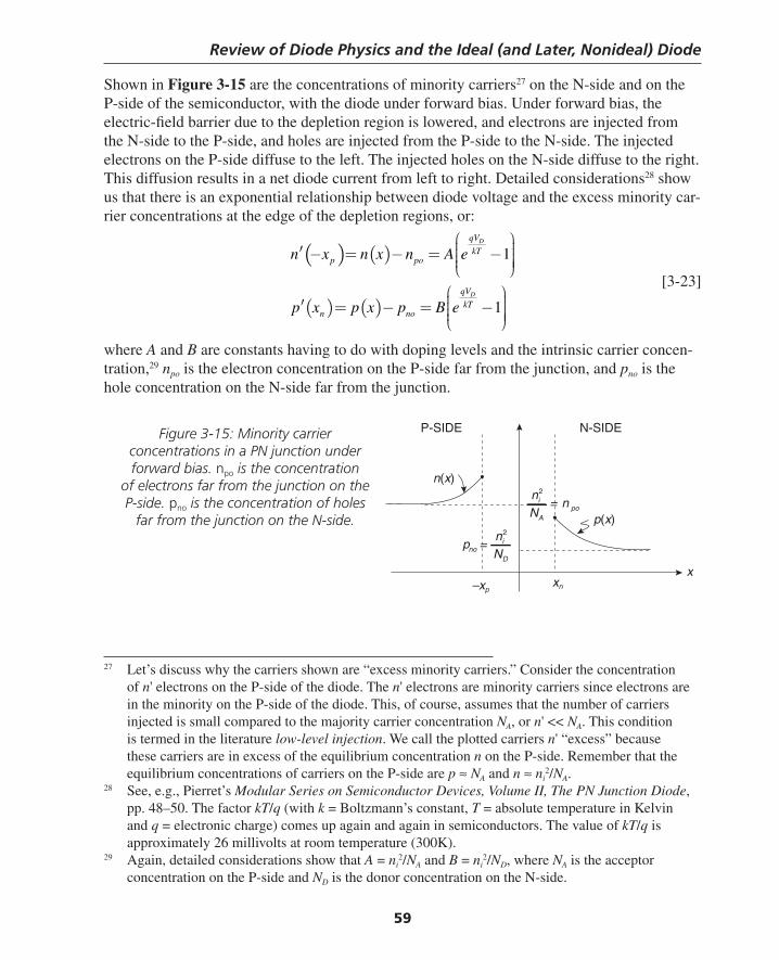
Review of Diode Physics and the Ideal (and Later, Nonideal) Diode
59
Shown in Figure 3-15 are the concentrations of minority carriers27 on the N-side and on the P-side of the semiconductor, with the diode under forward bias. Under forward bias, the electric-fi eld barrier due to the depletion region is lowered, and electrons are injected from the N-side to the P-side, and holes are injected from the P-side to the N-side. The injected electrons on the P-side diffuse to the left. The injected holes on the N-side diffuse to the right. This diffusion results in a net diode current from left to right. Detailed considerations28 show us that there is an exponential relationship between diode voltage and the excess minority car-rier concentrations at the edge of the depletion regions, or:
( ) ( )
( ) ( )
1
1
D
D
qV
kTp po
qV
kTn no
n x n x n A e
p x p x p B e
⎛ ⎞⎟⎜ ⎟′ − = − = −⎜ ⎟⎜ ⎟⎟⎜⎝ ⎠⎛ ⎞⎟⎜ ⎟′ = − = −⎜ ⎟⎜ ⎟⎟⎜⎝ ⎠
[3-23]
where A and B are constants having to do with doping levels and the intrinsic carrier concen-tration,29 npo is the electron concentration on the P-side far from the junction, and pno is the hole concentration on the N-side far from the junction.
Figure 3-15: Minority carrier concentrations in a PN junction under forward bias. npo is the concentration
of electrons far from the junction on the P-side. pno is the concentration of holes
far from the junction on the N-side.
P-SIDE N-SIDE
x
n(x)
p(x)
–xpxn
2i
noD
np
N=
2i
poA
nn
N=
27 Let’s discuss why the carriers shown are “excess minority carriers.” Consider the concentration of n' electrons on the P-side of the diode. The n' electrons are minority carriers since electrons are in the minority on the P-side of the diode. This, of course, assumes that the number of carriers injected is small compared to the majority carrier concentration NA, or n' << NA. This condition is termed in the literature low-level injection. We call the plotted carriers n' “excess” because these carriers are in excess of the equilibrium concentration n on the P-side. Remember that the equilibrium concentrations of carriers on the P-side are p ≈ NA and n ≈ ni
2/NA. 28 See, e.g., Pierret’s Modular Series on Semiconductor Devices, Volume II, The PN Junction Diode,
pp. 48–50. The factor kT/q (with k = Boltzmann’s constant, T = absolute temperature in Kelvin and q = electronic charge) comes up again and again in semiconductors. The value of kT/q is approximately 26 millivolts at room temperature (300K).
29 Again, detailed considerations show that A = ni2/NA and B = ni
2/ND, where NA is the acceptor concentration on the P-side and ND is the donor concentration on the N-side.
Thompson Book.indb 59 3/20/2006 11:34:01 AM
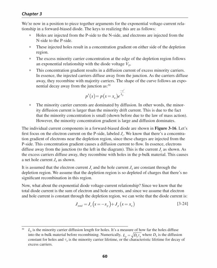
Chapter 3
60
We’re now in a position to piece together arguments for the exponential voltage-current rela-tionship in a forward-biased diode. The keys to realizing this are as follows:
• Holes are injected from the P-side to the N-side, and electrons are injected from the N-side to the P-side.
• These injected holes result in a concentration gradient on either side of the depletion region.
• The excess minority carrier concentration at the edge of the depletion region follows an exponential relationship with the diode voltage VD.
• This concentration gradient results in a diffusion current of excess minority carriers. In essence, the injected carriers diffuse away from the junction. As the carriers diffuse away, they recombine with majority carriers. The shape of the curve follows an expo-nential decay away from the junction as:30
( ) ( ) p
x
L
np x p x x e
′−
′ = =
• The minority carrier currents are dominated by diffusion. In other words, the minor-ity diffusion current is larger than the minority drift current. This is due to the fact that the minority concentration is small (shown before due to the law of mass action). However, the minority concentration gradient is large and diffusion dominates.
The individual current components in a forward-biased diode are shown in Figure 3-16. Let’s fi rst focus on the electron current on the P-side, labeled Je. We know that there’s a concentra-tion gradient of electrons near the depletion region, since these charges are injected from the P-side. This concentration gradient causes a diffusion current to fl ow. In essence, electrons diffuse away from the junction (to the left in the diagram). This is the current Je as shown. As the excess carriers diffuse away, they recombine with holes in the p-bulk material. This causes a net hole current Jh as shown.
It is assumed that the electron current Je and the hole current Jh are constant through the depletion region. We assume that the depletion region is so depleted of charges that there’s no signifi cant recombination in this region.
Now, what about the exponential diode voltage-current relationship? Since we know that the total diode current is the sum of electron and hole currents, and since we assume that electron and hole current is constant through the depletion region, we can write that the diode current is:
( ) ( )total e p p nJ J x x J x x= = − + = [3-24]
30 Lp is the minority carrier diffusion length for holes. It’s a measure of how far the holes diffuse into the n-bulk material before recombining. Numerically, L Dp h h= τ where Dh is the diffusion constant for holes and τh is the minority carrier lifetime, or the characteristic lifetime for decay of excess carriers.
Thompson Book.indb 60 3/20/2006 11:34:02 AM
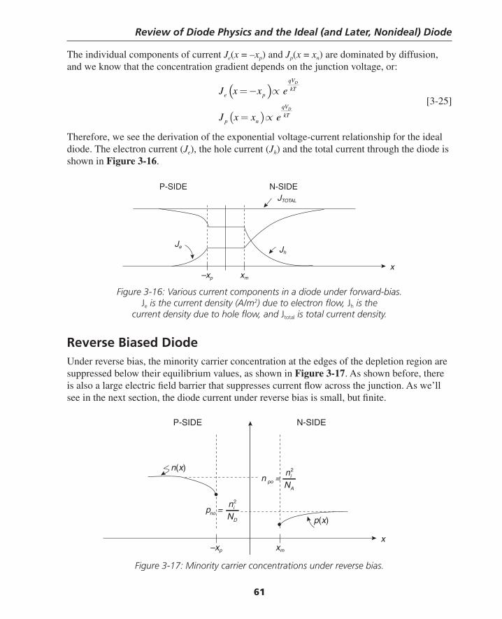
Review of Diode Physics and the Ideal (and Later, Nonideal) Diode
61
The individual components of current Je(x = –xp) and Jp(x = xn) are dominated by diffusion, and we know that the concentration gradient depends on the junction voltage, or:
( )
( )
D
D
qV
kTe p
qV
kTp n
J x x e
J x x e
∝
∝
= −
=
[3-25]
Therefore, we see the derivation of the exponential voltage-current relationship for the ideal diode. The electron current (Je), the hole current (Jh) and the total current through the diode is shown in Figure 3-16.
Figure 3-16: Various current components in a diode under forward-bias. Je is the current density (A/m2) due to electron fl ow, Jh is the
current density due to hole fl ow, and Jtotal is total current density.
Reverse Biased DiodeUnder reverse bias, the minority carrier concentration at the edges of the depletion region are suppressed below their equilibrium values, as shown in Figure 3-17. As shown before, there is also a large electric fi eld barrier that suppresses current fl ow across the junction. As we’ll see in the next section, the diode current under reverse bias is small, but fi nite.
P-SIDE N-SIDE
x
JTOTAL
Je Jh
xm–xp
P-SIDE N-SIDE
xxm–xp
n(x)
p(x)
2i
noD
np
N=
2i
poA
nn
N=
Figure 3-17: Minority carrier concentrations under reverse bias.
Thompson Book.indb 61 3/20/2006 11:34:02 AM
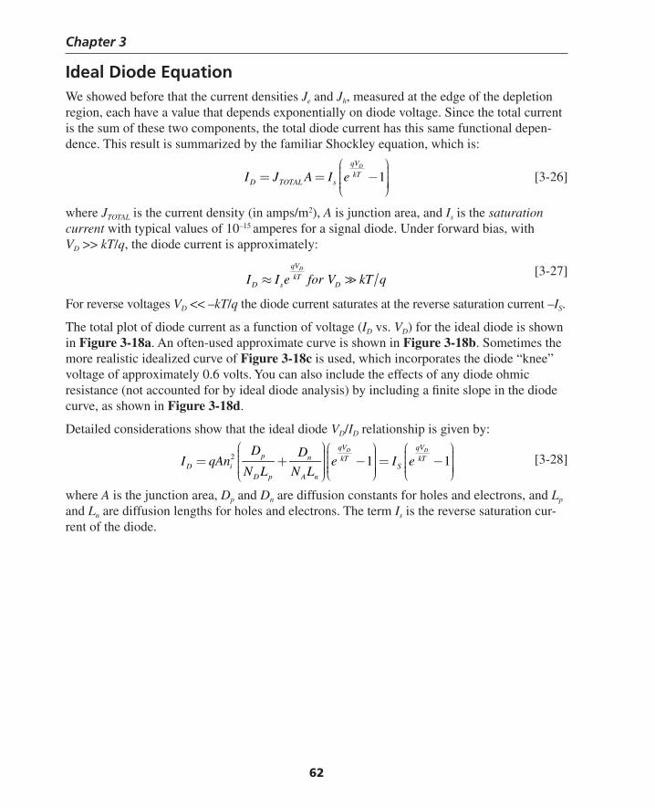
Chapter 3
62
Ideal Diode EquationWe showed before that the current densities Je and Jh, measured at the edge of the depletion region, each have a value that depends exponentially on diode voltage. Since the total current is the sum of these two components, the total diode current has this same functional depen-dence. This result is summarized by the familiar Shockley equation, which is:
1DqV
kTD TOTAL sI J A I e
⎛ ⎞⎟⎜ ⎟= = −⎜ ⎟⎜ ⎟⎟⎜⎝ ⎠ [3-26]
where JTOTAL is the current density (in amps/m2), A is junction area, and Is is the saturation current with typical values of 10–15
amperes for a signal diode. Under forward bias, with VD >> kT/q, the diode current is approximately:
DqV
kTD s DI I e for V kT q≈
[3-27]
For reverse voltages VD << –kT/q the diode current saturates at the reverse saturation current –IS.
The total plot of diode current as a function of voltage (ID vs. VD) for the ideal diode is shown in Figure 3-18a. An often-used approximate curve is shown in Figure 3-18b. Sometimes the more realistic idealized curve of Figure 3-18c is used, which incorporates the diode “knee” voltage of approximately 0.6 volts. You can also include the effects of any diode ohmic resistance (not accounted for by ideal diode analysis) by including a fi nite slope in the diode curve, as shown in Figure 3-18d.
Detailed considerations show that the ideal diode VD/ID relationship is given by:
2 1 1D DqV qV
p n kT kTD i S
D p A n
D DI qAn e I e
N L N L
⎛ ⎞⎛ ⎞ ⎛ ⎞⎟ ⎟ ⎟⎜ ⎜ ⎜⎟ ⎟ ⎟⎜= + − = −⎜ ⎜⎟ ⎟ ⎟⎜ ⎜ ⎜⎟ ⎟ ⎟⎟ ⎟⎜ ⎜⎜ ⎟⎝ ⎠ ⎝ ⎠⎝ ⎠ [3-28]
where A is the junction area, Dp and Dn are diffusion constants for holes and electrons, and Lp and Ln are diffusion lengths for holes and electrons. The term Is is the reverse saturation cur-rent of the diode.
Thompson Book.indb 62 3/20/2006 11:34:03 AM
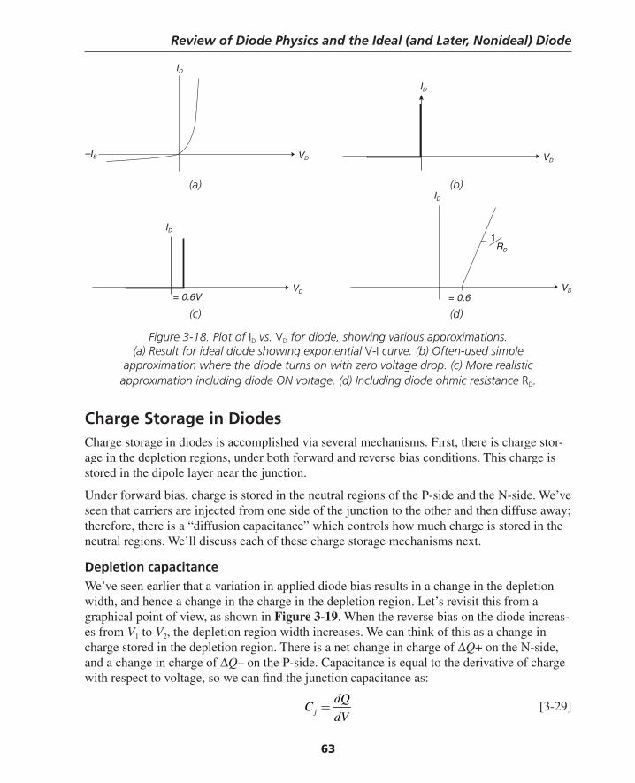
Review of Diode Physics and the Ideal (and Later, Nonideal) Diode
63
(a) (b)
VD VD
VD
ID
–IS
ID
ID
= 0.6VVD
ID
= 0.6
1RD
(c) (d)
Figure 3-18. Plot of ID vs. VD for diode, showing various approximations. (a) Result for ideal diode showing exponential V-I curve. (b) Often-used simple
approximation where the diode turns on with zero voltage drop. (c) More realistic approximation including diode ON voltage. (d) Including diode ohmic resistance RD.
Charge Storage in DiodesCharge storage in diodes is accomplished via several mechanisms. First, there is charge stor-age in the depletion regions, under both forward and reverse bias conditions. This charge is stored in the dipole layer near the junction.
Under forward bias, charge is stored in the neutral regions of the P-side and the N-side. We’ve seen that carriers are injected from one side of the junction to the other and then diffuse away; therefore, there is a “diffusion capacitance” which controls how much charge is stored in the neutral regions. We’ll discuss each of these charge storage mechanisms next.
Depletion capacitanceWe’ve seen earlier that a variation in applied diode bias results in a change in the depletion width, and hence a change in the charge in the depletion region. Let’s revisit this from a graphical point of view, as shown in Figure 3-19. When the reverse bias on the diode increas-es from V1 to V2, the depletion region width increases. We can think of this as a change in charge stored in the depletion region. There is a net change in charge of ΔQ+ on the N-side, and a change in charge of ΔQ– on the P-side. Capacitance is equal to the derivative of charge with respect to voltage, so we can fi nd the junction capacitance as:
j
dQC
dV= [3-29]
Thompson Book.indb 63 3/20/2006 11:34:04 AM

Chapter 3
64
x
ρ(x)
–qNA
qNDV2
V1
x
+ΔQ
–ΔQ
Figure 3-19: Illustration of cause of diode junction capacitance. As the
reverse bias increases from V1 to V2, the depletion width increases resulting in
an increase in depletion charge +ΔQ and –ΔQ on either sides of the junction.
–10 –8 –6 –4 –2 0 20
0.5
1
1.5
2
2.5
3
Nor
mal
ized
junc
tion
capa
cita
nce
31 This simple junction capacitance equation works well assuming that VD < φbi. Note that this equation shows a junction capacitance that increases without bound as VD → φbi.
A detailed analysis shows that the junction capacitance can be expressed as:
1
joj m
D
bi
CC
V
φ
=⎛ ⎞⎟⎜ ⎟−⎜ ⎟⎜ ⎟⎜⎝ ⎠
[3-30]
where m = 1/2 for an abrupt junction and m = 1/3 for a linearly graded junction. The term Cjo is the diode capacitance at zero diode voltage, and φbi is the built-in voltage. The junction voltage for a typical signal diode is plotted in Figure 3-20. Note that as reverse-bias voltage increases, the junction capacitance decreases. 31
Figure 3-20: Nonlinear junction capacitance vs. diode voltage for abrupt junction diode, shown for φbi = 0.8V and Cjo = 1.
Thompson Book.indb 64 3/20/2006 11:34:04 AM
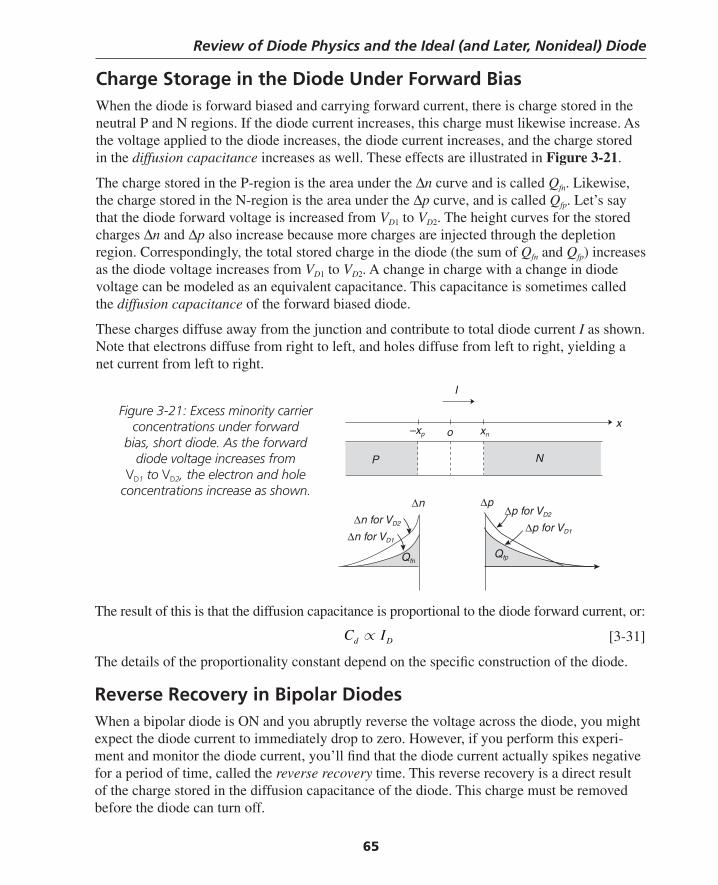
Review of Diode Physics and the Ideal (and Later, Nonideal) Diode
65
Charge Storage in the Diode Under Forward BiasWhen the diode is forward biased and carrying forward current, there is charge stored in the neutral P and N regions. If the diode current increases, this charge must likewise increase. As the voltage applied to the diode increases, the diode current increases, and the charge stored in the diffusion capacitance increases as well. These effects are illustrated in Figure 3-21.
The charge stored in the P-region is the area under the Δn curve and is called Qfn. Likewise, the charge stored in the N-region is the area under the Δp curve, and is called Qfp. Let’s say that the diode forward voltage is increased from VD1 to VD2. The height curves for the stored charges Δn and Δp also increase because more charges are injected through the depletion region. Correspondingly, the total stored charge in the diode (the sum of Qfn and Qfp) increases as the diode voltage increases from VD1 to VD2. A change in charge with a change in diode voltage can be modeled as an equivalent capacitance. This capacitance is sometimes called the diffusion capacitance of the forward biased diode.
These charges diffuse away from the junction and contribute to total diode current I as shown. Note that electrons diffuse from right to left, and holes diffuse from left to right, yielding a net current from left to right.
The result of this is that the diffusion capacitance is proportional to the diode forward current, or:
d DC I∝ [3-31]
The details of the proportionality constant depend on the specifi c construction of the diode.
Reverse Recovery in Bipolar DiodesWhen a bipolar diode is ON and you abruptly reverse the voltage across the diode, you might expect the diode current to immediately drop to zero. However, if you perform this experi-ment and monitor the diode current, you’ll fi nd that the diode current actually spikes negative for a period of time, called the reverse recovery time. This reverse recovery is a direct result of the charge stored in the diffusion capacitance of the diode. This charge must be removed before the diode can turn off.
x
Δn for VD2
I
–xp xno
P N
Δn for VD1
Δn ΔpΔp for VD2
Δp for VD1
QfnQfp
Figure 3-21: Excess minority carrier concentrations under forward
bias, short diode. As the forward diode voltage increases from
VD1 to VD2, the electron and hole concentrations increase as shown.
Thompson Book.indb 65 3/20/2006 11:34:05 AM
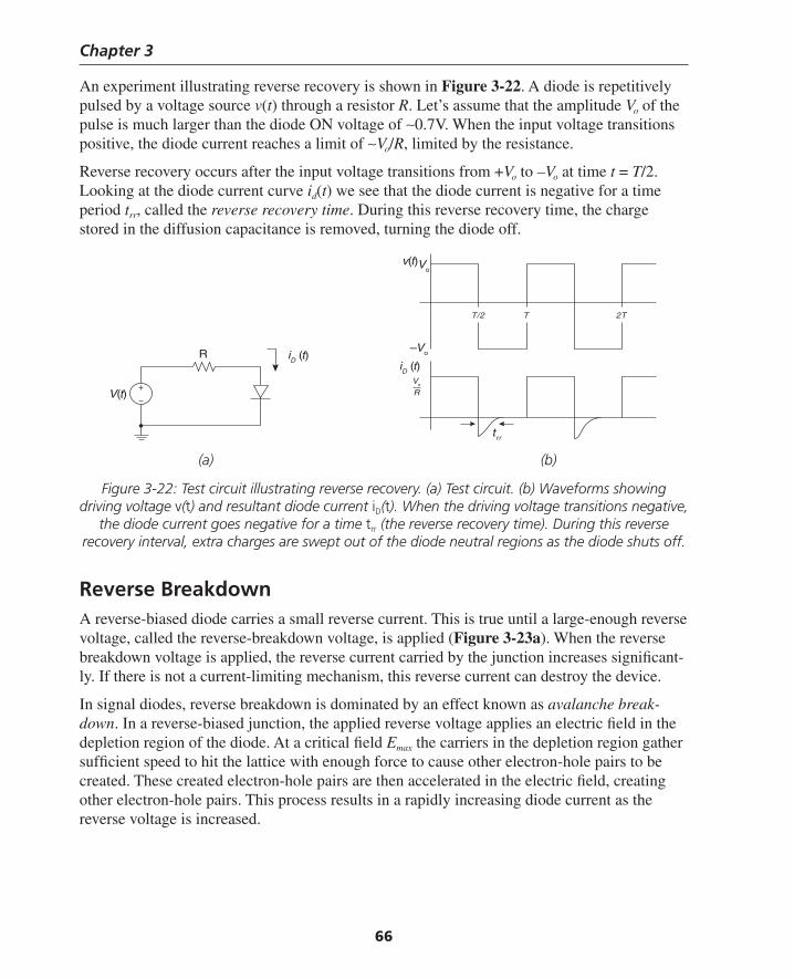
Chapter 3
66
An experiment illustrating reverse recovery is shown in Figure 3-22. A diode is repetitively pulsed by a voltage source v(t) through a resistor R. Let’s assume that the amplitude Vo of the pulse is much larger than the diode ON voltage of ∼0.7V. When the input voltage transitions positive, the diode current reaches a limit of ∼Vo/R, limited by the resistance.
Reverse recovery occurs after the input voltage transitions from +Vo to –Vo at time t = T/2. Looking at the diode current curve id(t) we see that the diode current is negative for a time period trr, called the reverse recovery time. During this reverse recovery time, the charge stored in the diffusion capacitance is removed, turning the diode off.
(a) (b)
Figure 3-22: Test circuit illustrating reverse recovery. (a) Test circuit. (b) Waveforms showing driving voltage v(t) and resultant diode current iD(t). When the driving voltage transitions negative,
the diode current goes negative for a time trr (the reverse recovery time). During this reverse recovery interval, extra charges are swept out of the diode neutral regions as the diode shuts off.
Reverse BreakdownA reverse-biased diode carries a small reverse current. This is true until a large-enough reverse voltage, called the reverse-breakdown voltage, is applied (Figure 3-23a). When the reverse breakdown voltage is applied, the reverse current carried by the junction increases signifi cant-ly. If there is not a current-limiting mechanism, this reverse current can destroy the device.
In signal diodes, reverse breakdown is dominated by an effect known as avalanche break-down. In a reverse-biased junction, the applied reverse voltage applies an electric fi eld in the depletion region of the diode. At a critical fi eld Emax the carriers in the depletion region gather suffi cient speed to hit the lattice with enough force to cause other electron-hole pairs to be created. These created electron-hole pairs are then accelerated in the electric fi eld, creating other electron-hole pairs. This process results in a rapidly increasing diode current as the reverse voltage is increased.
R
V(t)
iD (t)
v(t)Vo
–Vo
iD (t)Vo
R
trr
T/2 T 2T
Thompson Book.indb 66 3/20/2006 11:34:05 AM
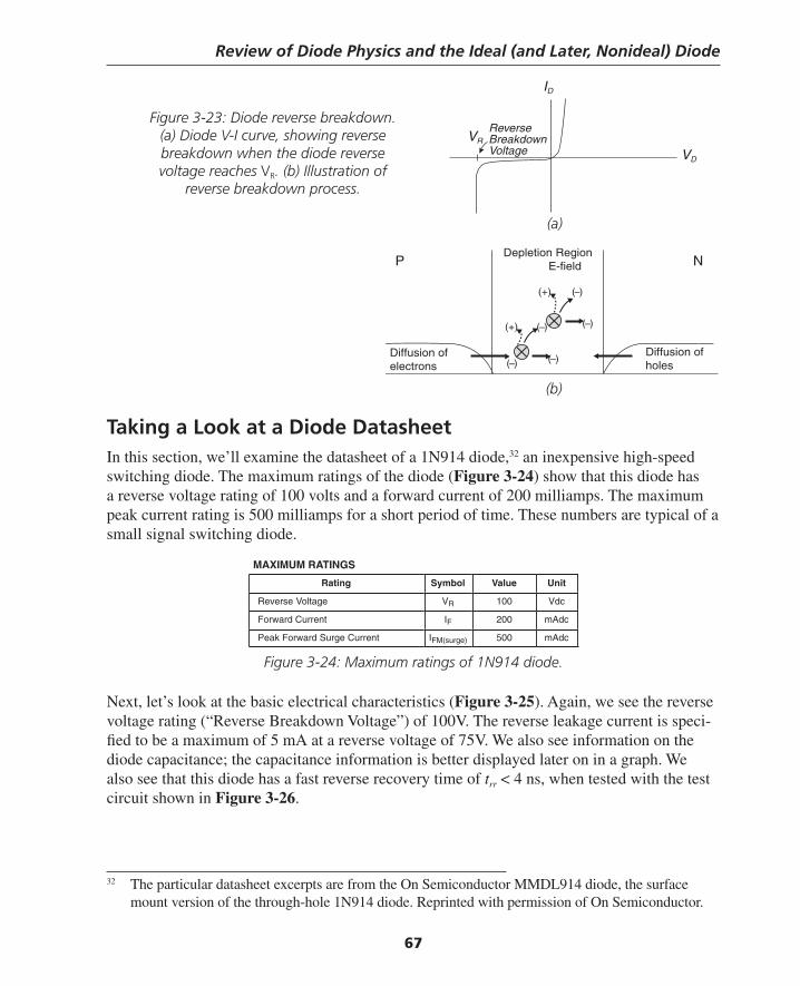
Review of Diode Physics and the Ideal (and Later, Nonideal) Diode
67
Taking a Look at a Diode DatasheetIn this section, we’ll examine the datasheet of a 1N914 diode,32 an inexpensive high-speed switching diode. The maximum ratings of the diode (Figure 3-24) show that this diode has a reverse voltage rating of 100 volts and a forward current of 200 milliamps. The maximum peak current rating is 500 milliamps for a short period of time. These numbers are typical of a small signal switching diode.
ID
VD
VR
Reverse BreakdownVoltage
P NDepletion Region E-field
Diffusion ofholes
Diffusion ofelectrons
(+)
(+)
(−)
(−)
(−)
(−)××(−)
(a)
(b)
Figure 3-23: Diode reverse breakdown. (a) Diode V-I curve, showing reverse breakdown when the diode reverse voltage reaches VR. (b) Illustration of
reverse breakdown process.
32 The particular datasheet excerpts are from the On Semiconductor MMDL914 diode, the surface mount version of the through-hole 1N914 diode. Reprinted with permission of On Semiconductor.
Figure 3-24: Maximum ratings of 1N914 diode.
Next, let’s look at the basic electrical characteristics (Figure 3-25). Again, we see the reverse voltage rating (“Reverse Breakdown Voltage”) of 100V. The reverse leakage current is speci-fi ed to be a maximum of 5 mA at a reverse voltage of 75V. We also see information on the diode capacitance; the capacitance information is better displayed later on in a graph. We also see that this diode has a fast reverse recovery time of trr < 4 ns, when tested with the test circuit shown in Figure 3-26.
MAXIMUM RATINGS
Rating Symbol Value Unit
Reverse Voltage VR 100 Vdc
Forward Current IF 200 mAdc
Peak Forward Surge Current IFM(surge) 500 mAdc
Thompson Book.indb 67 3/20/2006 11:34:05 AM
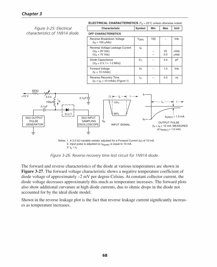
Chapter 3
68
Figure 3-25: Electrical characteristics of 1N914 diode.
Figure 3-26: Reverse recovery time test circuit for 1N914 diode.
The forward and reverse characteristics of the diode at various temperatures are shown in Figure 3-27. The forward voltage characteristic shows a negative temperature coeffi cient of diode voltage of approximately –2 mV per degree Celsius. At constant collector current, the diode voltage decreases approximately this much as temperature increases. The forward plots also show additional curvature at high diode currents, due to ohmic drops in the diode not accounted for by the ideal diode model.
Shown in the reverse leakage plot is the fact that reverse leakage current signifi cantly increas-es as temperature increases.
ELECTRICAL CHARACTERISTICS (TA = 25°C unless otherwise noted)
Characteristic Symbol Min Max Unit
OFF CHARACTERISTICS
Reverse Breakdown Voltage(IR = 100 Adc)
V(BR) 100 − Vdc
Reverse Voltage Leakage Current (VR = 20 Vdc)(VR = 75 Vdc)
IR−−
255.0
nAdcAdc
Diode Capacitance(VR = 0 V, f = 1.0 MHz)
CT − 4.0 pF
Forward Voltage (IF = 10 mAdc)
VF − 1.0 Vdc
Reverse Recovery Time (IF = IR = 10 mAdc) (Figure 1)
trr − 4.0 ns
Notes: 1. A 2.0 k variable resistor adjusted for a Forward Current (IF) of 10 mA.Notes: 2. Input pulse is adjusted so IR(peak) is equal to 10 mA.Notes: 3. tp » trr
+10 V 2.0 k
820
0.1 F
D.U.T.
VR
100 H0.1 F
50 OUTPUTPULSE
GENERATOR
50 INPUTSAMPLING
OSCILLOSCOPE
tr tp t
10%
90%
IF
IR
trr t
iR(REC) = 1.0 mA
OUTPUT PULSE(IF = IR = 10 mA; MEASURED
at iR(REC) = 1.0 mA)
IF
INPUT SIGNAL
Thompson Book.indb 68 3/20/2006 11:34:06 AM
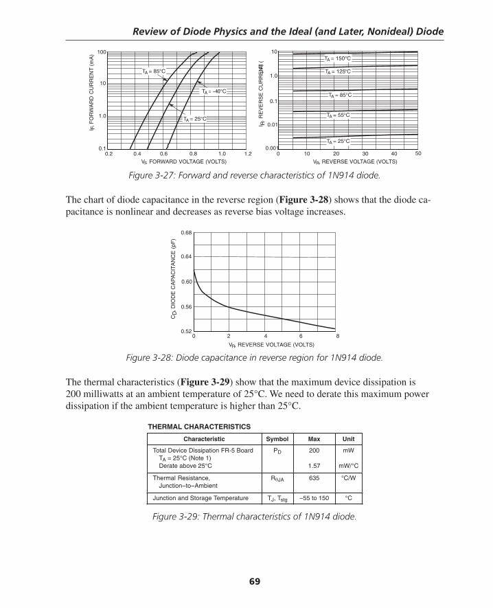
Review of Diode Physics and the Ideal (and Later, Nonideal) Diode
69
Figure 3-27: Forward and reverse characteristics of 1N914 diode.
The chart of diode capacitance in the reverse region (Figure 3-28) shows that the diode ca-pacitance is nonlinear and decreases as reverse bias voltage increases.
100
0.2 0.4
VF, FORWARD VOLTAGE (VOLTS)
0.6 0.8 1.0 1.2
10
1.0
0.1
TA = 85°C
10
0
VR, REVERSE VOLTAGE (VOLTS)
1.0
0.1
0.01
0.00110 20 30 40 50
I F, F
OR
WA
RD
CU
RR
EN
T (
mA
)TA °C
TA = 25°C
TA = 150°C
TA = 125°C
TA = 85°C
TA = 55°C
TA = 25°C
I R,
RE
VE
RS
E C
UR
RE
NT
(µ
A)
0.68
0
VR, REVERSE VOLTAGE (VOLTS)
0.64
0.60
0.56
0.52
CD
, DIO
DE
CA
PA
CIT
AN
CE
(pF
)
2 4 6 8
Figure 3-28: Diode capacitance in reverse region for 1N914 diode.
The thermal characteristics (Figure 3-29) show that the maximum device dissipation is 200 milliwatts at an ambient temperature of 25°C. We need to derate this maximum power dissipation if the ambient temperature is higher than 25°C.
THERMAL CHARACTERISTICS
Characteristic Symbol Max Unit
Total Device Dissipation FR-5 BoardTA = 25°C (Note 1)Derate above 25°C
PD 200
1.57
mW
mW/°C
Thermal Resistance,Junction−to−Ambient
R JA 635 °C/W
Junction and Storage Temperature TJ, Tstg −55 to 150 °C
Figure 3-29: Thermal characteristics of 1N914 diode.
Thompson Book.indb 69 3/20/2006 11:34:06 AM
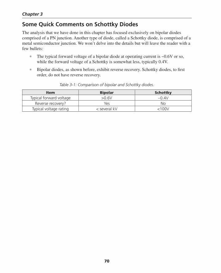
Chapter 3
70
Some Quick Comments on Schottky DiodesThe analysis that we have done in this chapter has focused exclusively on bipolar diodes comprised of a PN junction. Another type of diode, called a Schottky diode, is comprised of a metal semiconductor junction. We won’t delve into the details but will leave the reader with a few bullets:
• The typical forward voltage of a bipolar diode at operating current is ~0.6V or so, while the forward voltage of a Schottky is somewhat less, typically 0.4V.
• Bipolar diodes, as shown before, exhibit reverse recovery. Schottky diodes, to fi rst order, do not have reverse recovery.
Table 3-1: Comparison of bipolar and Schottky diodes.
Item Bipolar SchottkyTypical forward voltage >0.6V ∼0.4V
Reverse recovery? Yes NoTypical voltage rating < several kV <100V
Thompson Book.indb 70 3/20/2006 11:34:07 AM
71
Chapter 3 Problems
Problem 3.1For the ideal diode under forward bias, fi nd the amount of forward voltage increase that causes a 10× increase in forward current at room temperature.
Problem 3.2An abrupt PN+ junction diode has ND = 1016/cm3 and NA = 1015/cm3. Find the breakdown voltage if the breakdown electric fi eld Emax = 3 × 10⁵ V/cm. Assume the abrupt junction ap-proximation, an intrinsic carrier concentration in silicon of ni = 1.5 × 10¹⁰/cm3, that the diode operates at room temperature, and note that the total depletion region width with an applied bias VD is:
( )2 1 1Si bi D
n pA D
Vx x
q N N
ε φ ⎛ ⎞− ⎟⎜ ⎟+ = +⎜ ⎟⎜ ⎟⎜⎝ ⎠ [3-32]
Problem 3.3An abrupt PN junction has parameters NA = 1017/cm3, ND = 1016/cm3, and area A = 10–3 cm2. Find the forward voltage at a forward current ID = 10 milliamps. For this diode at 300K, as-sume that mobilities are: μn = 1400 cm2V–1s–1, μp = 400 cm2V–1s–1, the minority carrier lifetimes are τn = τp = 10–6 seconds, and that the intrinsic carrier concentration is ni = 1.4 × 1010 cm–3.
Problem 3.4A diode has a reverse saturation current IS = 15 nanoamps at room temperature (298K). Plot the diode ID/VD curve over the voltage range –10V < VD < +0.5V, and at room temperature (∼27°C, or 300K) and at elevated temperature of 150C (423K). Assume the rule-of-thumb that the reverse current of a diode doubles for every 10°C increase in temperature.
Problem 3.5This problem investigates the use of load lines.33 The ideal diode of Problem 3.3 above is used in a simple circuit, biased from a +12V source through a 1-kΩ resistor. Assume that the diode
33 The load line method is a graphical method used to solve nonlinear equations. By plotting the characteristic diode curve and then plotting the curve imposed by an external resistive element and noting the intersection of the two plots we determine the operating point of the circuit. This method is also very useful for analyzing transistor circuits.
Thompson Book.indb 71 3/20/2006 11:34:07 AM
Chapter 3
72
operates at room temperature (300K) and hence kT/q = 26 mV. Find the diode current and diode voltage by the following methods:
(a) First, assume that the diode ON voltage is a constant 0.6V, regardless of diode cur-rent. Solve for diode current ID given this assumption.
(b) In a more detailed analysis, solve iteratively the diode equation and resistor load line equation to fi nd diode current and diode voltage, assuming that the diode reverse saturation current IS = 10–10A.
(c) Plot the diode current/voltage load line, indicating the operating point on your plot.
Problem 3.6Consider the diode circuit shown in Figure 3-30. The diode is biased with bias current source ID, and a small signal AC current source is also connected, id. The diode voltage has both a DC part, VD, and a small-signal varying part vd. The total diode current is given by:
1Dqv
kTD si I e
⎛ ⎞⎟⎜ ⎟= −⎜ ⎟⎜ ⎟⎟⎜⎝ ⎠ [3-33]
The diode current and diode voltage can be expressed as a DC part plus an incrementally varying part.
D D D
D D d
i I i
v V v
= +
= + [3-34]
Assume that the diode is biased in its forward-active region and that the value of the id is very small.
(a) Find the ratio of small-signal voltage to small-signal current, or vd/id.
(b) Draw the low-frequency small-signal model relating vd to id.
ID id
ID + id
+
–
VD + vd
Figure 3-30: Diode circuit for Problem 3.6.
Problem 3.7Shown in Figure 3-31 is a circuit containing a 1N4001 diode. Draw the load line and fi nd the diode current and diode power dissipation.
Thompson Book.indb 72 3/20/2006 11:34:07 AM
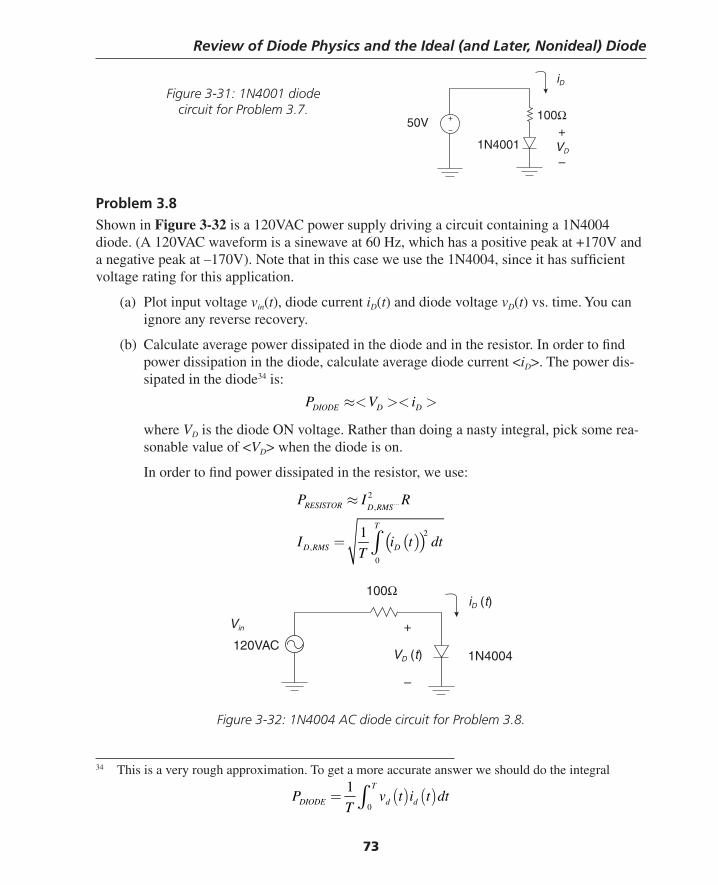
Review of Diode Physics and the Ideal (and Later, Nonideal) Diode
73
Problem 3.8Shown in Figure 3-32 is a 120VAC power supply driving a circuit containing a 1N4004 diode. (A 120VAC waveform is a sinewave at 60 Hz, which has a positive peak at +170V and a negative peak at –170V). Note that in this case we use the 1N4004, since it has suffi cient voltage rating for this application.
(a) Plot input voltage vin(t), diode current iD(t) and diode voltage vD(t) vs. time. You can ignore any reverse recovery.
(b) Calculate average power dissipated in the diode and in the resistor. In order to fi nd power dissipation in the diode, calculate average diode current <iD>. The power dis-sipated in the diode34 is:
DIODE D DP V i≈< >< >
where VD is the diode ON voltage. Rather than doing a nasty integral, pick some rea-sonable value of <VD> when the diode is on.
In order to fi nd power dissipated in the resistor, we use:
( )( )
2
,
2
,
0
1
RESISTOR D RMS
T
D RMS D
P I R
I i t dtT
≈
= ∫
Figure 3-32: 1N4004 AC diode circuit for Problem 3.8.
50V
1N4001+VD
–
100Ω
iD
120VAC1N4004
+
VD (t)
–
100ΩiD (t)
Vin
Figure 3-31: 1N4001 diode circuit for Problem 3.7.
34 This is a very rough approximation. To get a more accurate answer we should do the integral
PT
v t i t dtDIODE d d
T
= ( ) ( )∫1
0
Thompson Book.indb 73 3/20/2006 11:34:08 AM

Chapter 3
74
ReferencesAdler, R. B., Smith, A. C., and Longini, R. L., Introduction to Semiconductor Physics, Semi-
conductor Electronics Education Committee, volume 1, John Wiley, 1964.Bardeen, John, “Semiconductor Research Leading to the Point Contact Transistor,” December
11, 1956, from Nobel Lectures Physics, 1942-1962, Elsevier Publishing, available from the Nobel e-museum at Web: http://www.nobel.se/physics/laureates/1956/
Brattain, Walter H., “Surface Properties of Semiconductors,” December 11, 1956, from Nobel Lectures Physics, 1942-1962, Elsevier Publishing, available from the Nobel e-museum at Web: http://www.nobel.se/physics/laureates/1956/
Feynman, Richard, Leighton, Ralph, and Sands, Matthew, The Feynman Lectures on Physics, Addison-Wesley, 1963.
Gray, P. E., DeWitt, D., Boothroyd, A. R., and Gibbons, J. F., Physical Electronics and Circuit Models for Transistors, (SEEC volume 2), John Wiley, 1964.
———, Physical Electronics and Circuit Models of Transistors, Semiconductor Electronics Education Committee, volume 2, John Wiley, 1964. Hannay, N. B., editor, Semiconduc-tors, American Chemical Society Nomograph Series, Reinhold Publishing Corp., 1959.
Gray, Paul, and Searle, Campbell, Electronic Principles Physics, Models and Circuits, John Wiley, 1967.
Haynes, J. R. and Shockley, W., “The Mobility and Life of Injected Holes and Electrons in Germanium,” Physical Review, vol. 81, p. 835, 1951.
———, Physical Review, vol. 75, p. 691, 1949.Pierret, Robert F., Modular Series on Solid State Devices, Volume 1: Semiconductor Funda-
mentals, Addison-Wesley, 1983.Shockley, William, “Transistor Electronics: Imperfections, Unipolar and Analog Transistors,”
Proceedings of the IRE, vol. 40, no. 11, November, 1952, pp. 1289–1313, reprinted in Proceedings of the IEEE, vol. 85, no. 12, December 1997, pp. 2055–2080.
———, “Circuit Element Utilizing Semiconductive Materials,” U.S. Patent #2,569,347, issued September 25, 1951 and “Semiconductor Amplifi er,” U.S. patent 2,502,488, issued April 5, 1950, found in “Semiconductor Amplifi er Patent,” Proceedings of the IEEE, vol. 86, no. 1, p. 36.
———, “Transistor Technology Evokes New Physics,” December 11, 1956, from Nobel Lectures Physics, 1942-1962, Elsevier Publishing, available from the Nobel e-museum at Web: http://www.nobel.se/physics/laureates/1956/
Thompson Book.indb 74 3/20/2006 11:34:09 AM
75
C H A P T E R 4Bipolar Transistor Models
A Little Bit of HistoryPioneering work on the bipolar junction transistor was done at Bell Laboratories1 in the late 1940s, with contributions from William Shockley, William Brattain, James Bardeen, and oth-ers. This team (led by Shockley) was challenged by Bell management to invent a solid-state switch to replace mechanical relays. They initially focused their efforts on devices fabricated from germanium. The fi rst device that demonstrated the transistor effect and current gain was the “point contact” transistor demonstrated in 19482 (Figure 4-1), which had a germanium crystal with closely spaced gold contacts on the upper surface. With this device, Bardeen and Brattain were able to demonstrate current gain.
In This Chapter
This chapter builds on the device model work done in the previous chapter and models for the ideal bipolar transistor are derived. Rather than deriving the full transistor equations, we will rely on results from the ideal diode and “talk through” intuitively how the bipolar transistor works. The NPN transistor is considered, but results obtained are germane to analysis of the PNP transistor as well. Most of this discussion will focus on operation of the bipolar transistor in the “forward-active” region, the region of operation where the transistor can be used as an amplifi er. In later chapters, we’ll extensively discuss operation of the transistor in the saturation and cutoff regions.
1 Bell Telephone Labs, in Murray Hill, New Jersey. The physical layout, performance, and physics of the point contact transistor is described in W. D. Bevitt’s book Transistors Handbook, chapter 3, and in Lo, et al., Transistor Electronics, chapter 1.14.
2 It was John Bardeen who coined the terms emitter, base, and collector. For instance, in an NPN transistor, the emitter emits electrons and the collector collects them. The “base” was the base of a germanium crystal. See, e.g., W. F. Brinkman, et al., “A History of the Invention of the Transistor and Where It Will Lead Us.” An excellent reference describing the invention and implementation of the point-contact transistor is given in John Bardeen’s 1956 Nobel lecture.
Thompson Book.indb 75 3/20/2006 11:34:09 AM
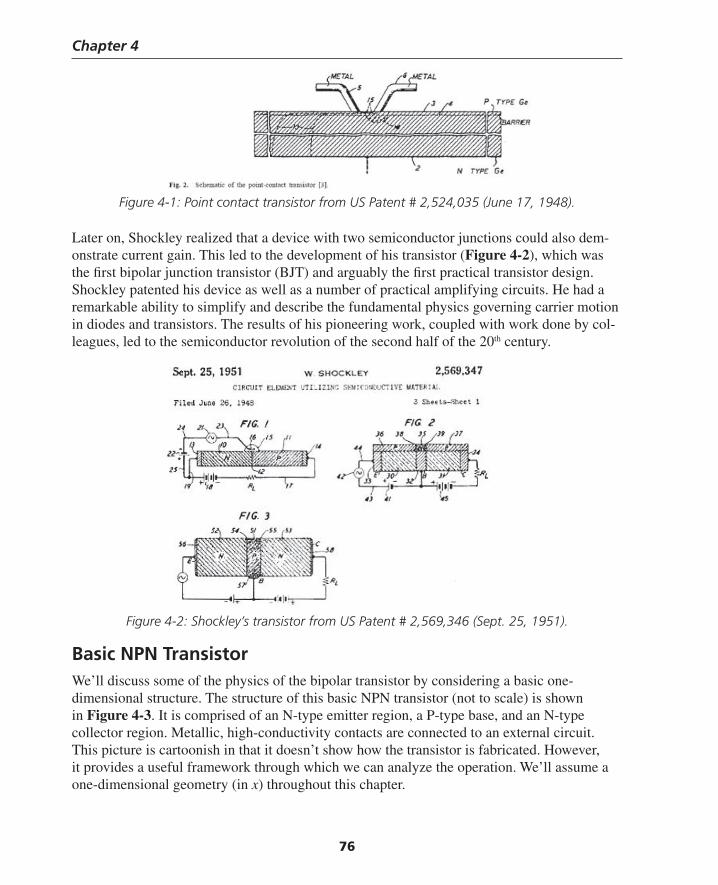
Chapter 4
76
Figure 4-1: Point contact transistor from US Patent # 2,524,035 (June 17, 1948).
Later on, Shockley realized that a device with two semiconductor junctions could also dem-onstrate current gain. This led to the development of his transistor (Figure 4-2), which was the fi rst bipolar junction transistor (BJT) and arguably the fi rst practical transistor design. Shockley patented his device as well as a number of practical amplifying circuits. He had a remarkable ability to simplify and describe the fundamental physics governing carrier motion in diodes and transistors. The results of his pioneering work, coupled with work done by col-leagues, led to the semiconductor revolution of the second half of the 20th century.
Figure 4-2: Shockley’s transistor from US Patent # 2,569,346 (Sept. 25, 1951).
Basic NPN TransistorWe’ll discuss some of the physics of the bipolar transistor by considering a basic one- dimensional structure. The structure of this basic NPN transistor (not to scale) is shown in Figure 4-3. It is comprised of an N-type emitter region, a P-type base, and an N-type collector region. Metallic, high-conductivity contacts are connected to an external circuit. This picture is cartoonish in that it doesn’t show how the transistor is fabricated. However, it provides a useful framework through which we can analyze the operation. We’ll assume a one-dimensional geometry (in x) throughout this chapter.
Thompson Book.indb 76 3/20/2006 11:34:09 AM
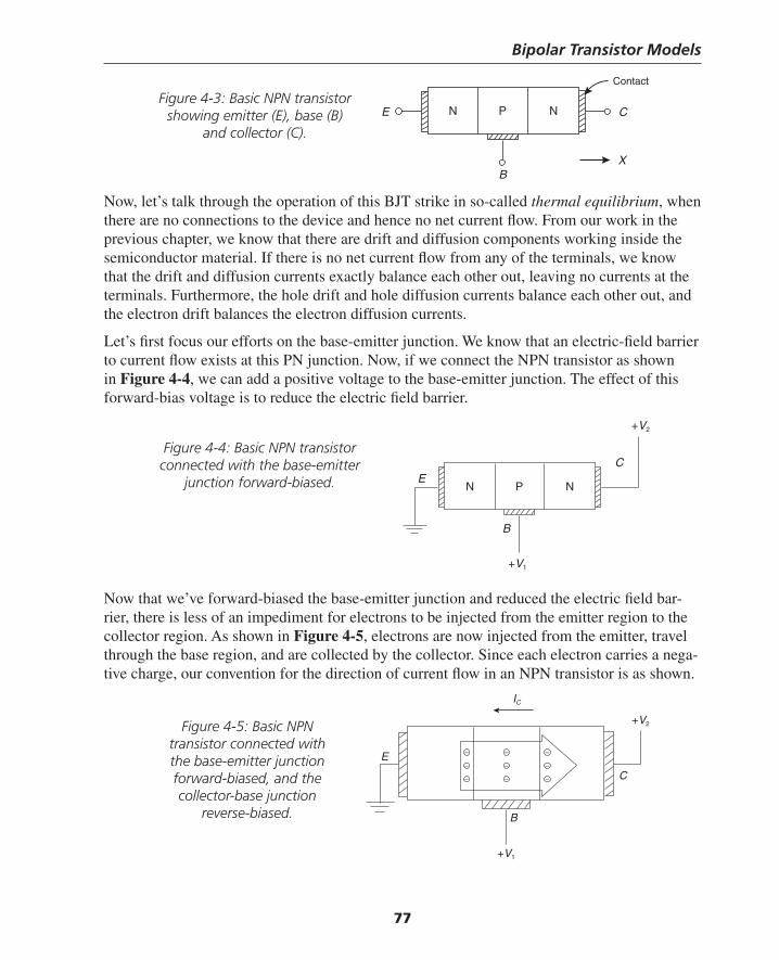
Bipolar Transistor Models
77
Now, let’s talk through the operation of this BJT strike in so-called thermal equilibrium, when there are no connections to the device and hence no net current fl ow. From our work in the previous chapter, we know that there are drift and diffusion components working inside the semiconductor material. If there is no net current fl ow from any of the terminals, we know that the drift and diffusion currents exactly balance each other out, leaving no currents at the terminals. Furthermore, the hole drift and hole diffusion currents balance each other out, and the electron drift balances the electron diffusion currents.
Let’s fi rst focus our efforts on the base-emitter junction. We know that an electric-fi eld barrier to current fl ow exists at this PN junction. Now, if we connect the NPN transistor as shown in Figure 4-4, we can add a positive voltage to the base-emitter junction. The effect of this forward-bias voltage is to reduce the electric fi eld barrier.
N NP
B
E C
X
Contact
Now that we’ve forward-biased the base-emitter junction and reduced the electric fi eld bar-rier, there is less of an impediment for electrons to be injected from the emitter region to the collector region. As shown in Figure 4-5, electrons are now injected from the emitter, travel through the base region, and are collected by the collector. Since each electron carries a nega-tive charge, our convention for the direction of current fl ow in an NPN transistor is as shown.
N NP
B
EC
+V2
+V1
B
E
C
+V2
+V1
IC
– – –
– – –
– – –
Figure 4-3: Basic NPN transistor showing emitter (E), base (B)
and collector (C).
Figure 4-4: Basic NPN transistor connected with the base-emitter
junction forward-biased.
Figure 4-5: Basic NPN transistor connected with the base-emitter junction forward-biased, and the collector-base junction
reverse-biased.
Thompson Book.indb 77 3/20/2006 11:34:10 AM
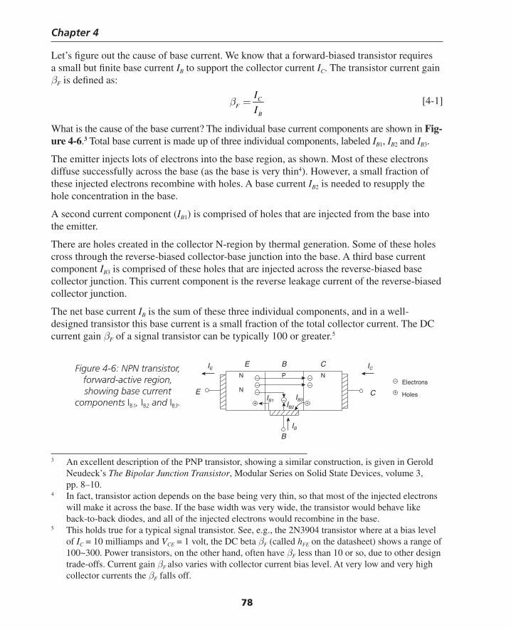
Chapter 4
78
Let’s fi gure out the cause of base current. We know that a forward-biased transistor requires a small but fi nite base current IB to support the collector current IC. The transistor current gain βF is defi ned as:
CF
B
I
Iβ = [4-1]
What is the cause of the base current? The individual base current components are shown in Fig-ure 4-6.3 Total base current is made up of three individual components, labeled IB1, IB2 and IB3.
The emitter injects lots of electrons into the base region, as shown. Most of these electrons diffuse successfully across the base (as the base is very thin4). However, a small fraction of these injected electrons recombine with holes. A base current IB2 is needed to resupply the hole concentration in the base.
A second current component (IB1) is comprised of holes that are injected from the base into the emitter.
There are holes created in the collector N-region by thermal generation. Some of these holes cross through the reverse-biased collector-base junction into the base. A third base current component IB3 is comprised of these holes that are injected across the reverse-biased base collector junction. This current component is the reverse leakage current of the reverse-biased collector junction.
The net base current IB is the sum of these three individual components, and in a well- designed transistor this base current is a small fraction of the total collector current. The DC current gain βF of a signal transistor can be typically 100 or greater.5
3 An excellent description of the PNP transistor, showing a similar construction, is given in Gerold Neudeck’s The Bipolar Junction Transistor, Modular Series on Solid State Devices, volume 3, pp. 8–10.
4 In fact, transistor action depends on the base being very thin, so that most of the injected electrons will make it across the base. If the base width was very wide, the transistor would behave like back-to-back diodes, and all of the injected electrons would recombine in the base.
5 This holds true for a typical signal transistor. See, e.g., the 2N3904 transistor where at a bias level of IC = 10 milliamps and VCE = 1 volt, the DC beta βF (called hFE on the datasheet) shows a range of 100~300. Power transistors, on the other hand, often have βF less than 10 or so, due to other design trade-offs. Current gain βF also varies with collector current bias level. At very low and very high collector currents the βF falls off.
B
E C
ICIEE B C
–– –– –
+ +
+
– N P N
N
IB
Electrons
HolesIB1IB2
IB3–
Figure 4-6: NPN transistor, forward-active region, showing base current
components IB1, IB2 and IB3.
Thompson Book.indb 78 3/20/2006 11:34:11 AM
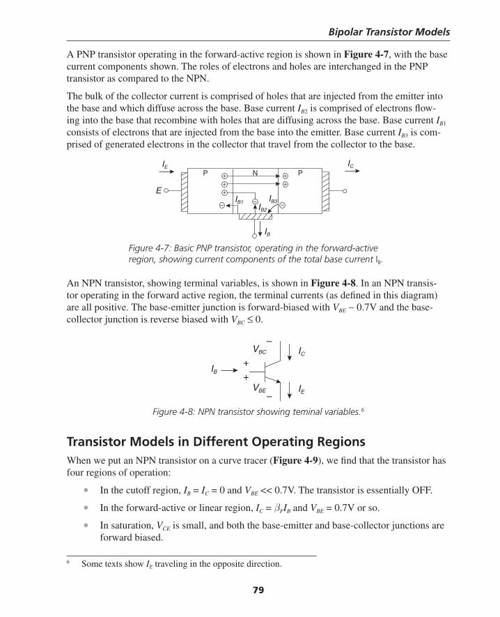
Bipolar Transistor Models
79
A PNP transistor operating in the forward-active region is shown in Figure 4-7, with the base current components shown. The roles of electrons and holes are interchanged in the PNP transistor as compared to the NPN.
The bulk of the collector current is comprised of holes that are injected from the emitter into the base and which diffuse across the base. Base current IB2 is comprised of electrons fl ow-ing into the base that recombine with holes that are diffusing across the base. Base current IB1 consists of electrons that are injected from the base into the emitter. Base current IB3 is com-prised of generated electrons in the collector that travel from the collector to the base.
An NPN transistor, showing terminal variables, is shown in Figure 4-8. In an NPN transis-tor operating in the forward active region, the terminal currents (as defi ned in this diagram) are all positive. The base-emitter junction is forward-biased with VBE ∼ 0.7V and the base- collector junction is reverse biased with VBC ≤ 0.
E
ICIE
++ ++ +
– –
P N P
IB
IB1IB2
IB3–
Figure 4-7: Basic PNP transistor, operating in the forward-active region, showing current components of the total base current IB.
Figure 4-8: NPN transistor showing teminal variables.6
Transistor Models in Different Operating RegionsWhen we put an NPN transistor on a curve tracer (Figure 4-9), we fi nd that the transistor has four regions of operation:
• In the cutoff region, IB = IC = 0 and VBE << 0.7V. The transistor is essentially OFF.
• In the forward-active or linear region, IC = βFIB and VBE = 0.7V or so.
• In saturation, VCE is small, and both the base-emitter and base-collector junctions are forward biased.
IC
IE
VBC
VBE
IB+
+
–
–
6 Some texts show IE traveling in the opposite direction.
Thompson Book.indb 79 3/20/2006 11:34:11 AM
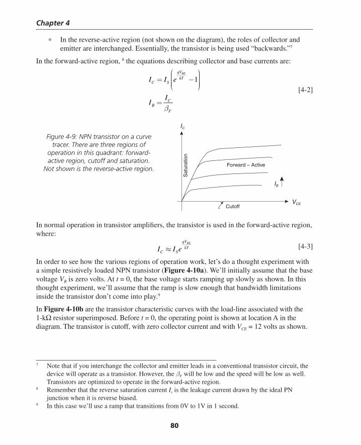
Chapter 4
80
• In the reverse-active region (not shown on the diagram), the roles of collector and emitter are interchanged. Essentially, the transistor is being used “backwards.”7
In the forward-active region, 8 the equations describing collector and base currents are:
1BEqV
kTC S
CB
F
I I e
II
β
⎛ ⎞⎟⎜ ⎟= −⎜ ⎟⎜ ⎟⎟⎜⎝ ⎠
=
[4-2]
7 Note that if you interchange the collector and emitter leads in a conventional transistor circuit, the device will operate as a transistor. However, the βF will be low and the speed will be low as well. Transistors are optimized to operate in the forward-active region.
8 Remember that the reverse saturation current Is is the leakage current drawn by the ideal PN junction when it is reverse biased.
9 In this case we’ll use a ramp that transitions from 0V to 1V in 1 second.
In normal operation in transistor amplifi ers, the transistor is used in the forward-active region, where:
BEqV
kTC SI I e≈ [4-3]
In order to see how the various regions of operation work, let’s do a thought experiment with a simple resistively loaded NPN transistor (Figure 4-10a). We’ll initially assume that the base voltage VB is zero volts. At t = 0, the base voltage starts ramping up slowly as shown. In this thought experiment, we’ll assume that the ramp is slow enough that bandwidth limitations inside the transistor don’t come into play.9
In Figure 4-10b are the transistor characteristic curves with the load-line associated with the 1-kΩ resistor superimposed. Before t = 0, the operating point is shown at location A in the diagram. The transistor is cutoff, with zero collector current and with VCE = 12 volts as shown.
IB
IC
VCE
Sat
urat
ion
Cutoff
Forward – Active
Figure 4-9: NPN transistor on a curve tracer. There are three regions of
operation in this quadrant: forward-active region, cutoff and saturation.
Not shown is the reverse-active region.
Thompson Book.indb 80 3/20/2006 11:34:12 AM
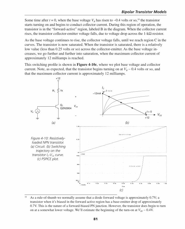
Bipolar Transistor Models
81
Some time after t = 0, when the base voltage VB has risen to ∼0.4 volts or so,10 the transistor starts turning on and begins to conduct collector current. During this region of operation, the transistor is in the “forward-active” region, labeled B in the diagram. When the collector current rises, the transistor collector-emitter voltage falls, due to voltage drop across the 1-kΩ resistor.
As the base voltage continues to rise, the collector voltage falls, until we reach region C in the curves. The transistor is now saturated. When the transistor is saturated, there is a relatively low value (less than 0.25 volts or so) across the collector-emitter. As the base voltage in-creases, we go further and further into saturation, when the maximum collector current of approximately 12 milliamps is reached.
This switching profi le is shown in Figure 4-10c, where we plot base voltage and collector current. Note, as expected, that the transistor begins turning on at VB ∼ 0.4 volts or so, and that the maximum collector current is approximately 12 milliamps.
10 As a rule-of-thumb we normally assume that a diode forward voltage is approximately 0.7V; a transistor when it’s biased in the forward active region has a base-emitter drop of approximately 0.7V. This is the nature of a forward-biased PN junction. However, the transistor does begin to turn on at a somewhat lower voltage. We’ll estimate the beginning of the turn-on at VBE ∼ 0.4V.
(a) (b)
+12
1kR1
VB
Q1
Q2N3904
+
VCE
−
IC
VCE
t → ∞
t = 0
+12
≈12mA
Figure 4-10: Resistively-loaded NPN transistor.
(a) Circuit. (b) Switching trajectory on the
transistor IC-VCE curve. (c) PSPICE plot.
(c)
Thompson Book.indb 81 3/20/2006 11:34:12 AM
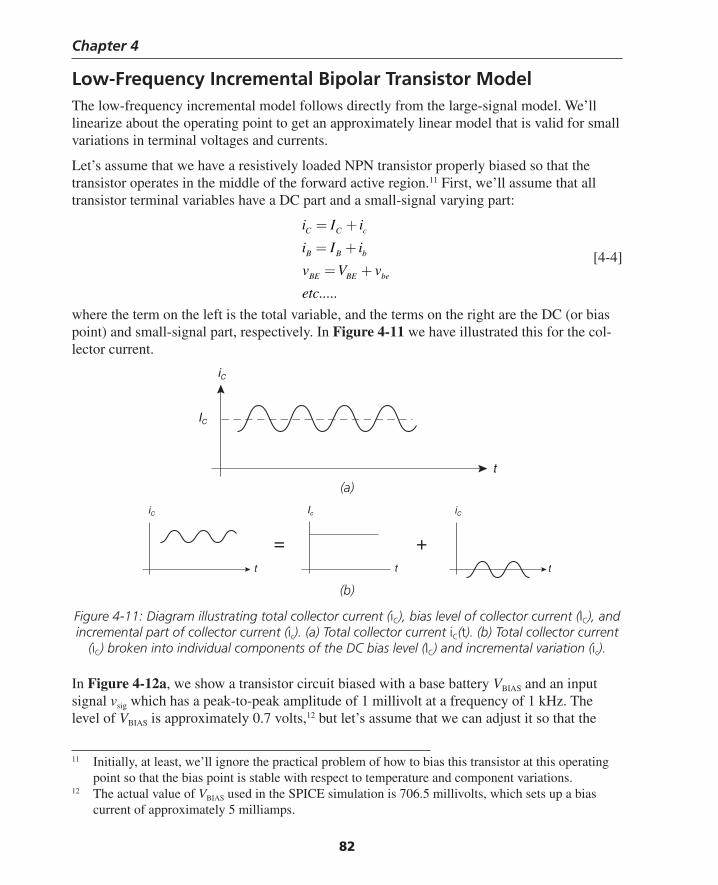
Chapter 4
82
11 Initially, at least, we’ll ignore the practical problem of how to bias this transistor at this operating point so that the bias point is stable with respect to temperature and component variations.
12 The actual value of VBIAS used in the SPICE simulation is 706.5 millivolts, which sets up a bias current of approximately 5 milliamps.
IC
iC
t
iC
t
iC
t
= +
Ic
t
Low-Frequency Incremental Bipolar Transistor ModelThe low-frequency incremental model follows directly from the large-signal model. We’ll linearize about the operating point to get an approximately linear model that is valid for small variations in terminal voltages and currents.
Let’s assume that we have a resistively loaded NPN transistor properly biased so that the transistor operates in the middle of the forward active region.11 First, we’ll assume that all transistor terminal variables have a DC part and a small-signal varying part:
.....
C C c
B B b
BE BE be
i I i
i I i
v V v
etc
= +
= +
= + [4-4]
where the term on the left is the total variable, and the terms on the right are the DC (or bias point) and small-signal part, respectively. In Figure 4-11 we have illustrated this for the col-lector current.
(a)
(b)
Figure 4-11: Diagram illustrating total collector current (iC), bias level of collector current (IC), and incremental part of collector current (ic). (a) Total collector current iC(t). (b) Total collector current
(iC) broken into individual components of the DC bias level (IC) and incremental variation (ic).
In Figure 4-12a, we show a transistor circuit biased with a base battery VBIAS and an input signal vsig which has a peak-to-peak amplitude of 1 millivolt at a frequency of 1 kHz. The level of VBIAS is approximately 0.7 volts,12 but let’s assume that we can adjust it so that the
Thompson Book.indb 82 3/20/2006 11:34:14 AM
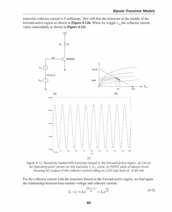
Bipolar Transistor Models
83
transistor collector current is 5 milliamps. This will bias the transistor in the middle of the forward-active region as shown in Figure 4-12b. When we wiggle vsig the collector current varies sinusoidally as shown in Figure 4-12c.
(a) (b)
+12
1kR1
vb
vsig
2N3904
vbias
706.50 mV
IC
VCE
12mA
5mA
7V 12V
(c)
Figure 4-12: Resistively loaded NPN transistor biased in the forward-active region. (a) Circuit. (b) Operating point shown on the transistor IC-VCE curve. (c) PSPICE plots of above circuit
showing AC output of the collector current riding on a DC bias level of ∼4.95 mA.
For the collector current with the transistor biased in the forward active region, we fi nd again the relationship between base-emitter voltage and collector current:
( )BE be beq V v qv
kT kTC c S CI i I e I e
+
+ ≈ = [4-5]
Thompson Book.indb 83 3/20/2006 11:34:14 AM
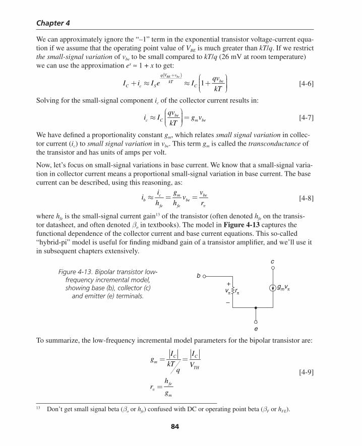
Chapter 4
84
We can approximately ignore the “–1” term in the exponential transistor voltage-current equa-tion if we assume that the operating point value of VBE is much greater than kT/q. If we restrict the small-signal variation of vbe to be small compared to kT/q (26 mV at room temperature) we can use the approximation ex ≈ 1 + x to get:
( )
1BE beq V v
bekTC c S C
qvI i I e I
kT
+ ⎛ ⎞⎟⎜+ ≈ ≈ + ⎟⎜ ⎟⎟⎜⎝ ⎠ [4-6]
Solving for the small-signal component ic of the collector current results in:
bec C m be
qvi I g v
kT
⎛ ⎞⎟⎜≈ =⎟⎜ ⎟⎟⎜⎝ ⎠ [4-7]
We have defi ned a proportionality constant gm, which relates small signal variation in collec-tor current (ic) to small signal variation in vbe. This term gm is called the transconductance of the transistor and has units of amps per volt.
Now, let’s focus on small-signal variations in base current. We know that a small-signal varia-tion in collector current means a proportional small-signal variation in base current. The base current can be described, using this reasoning, as:
c m beb be
fe fe
i g vi v
h h rπ
≈ = = [4-8]
where hfe is the small-signal current gain13 of the transistor (often denoted hfe on the transis-tor datasheet, and often denoted βo in textbooks). The model in Figure 4-13 captures the functional dependence of the collector current and base current equations. This so-called “hybrid-pi” model is useful for fi nding midband gain of a transistor amplifi er, and we’ll use it in subsequent chapters extensively.
13 Don’t get small signal beta (βo or hfe) confused with DC or operating point beta (βF or hFE).
+
–
b
rπ
e
gmvπvπ
c
Figure 4-13. Bipolar transistor low-frequency incremental model, showing base (b), collector (c)
and emitter (e) terminals.
To summarize, the low-frequency incremental model parameters for the bipolar transistor are:
C Cm
TH
fe
m
I Ig
kT Vq
hr
gπ
= =
=
[4-9]
Thompson Book.indb 84 3/20/2006 11:34:15 AM
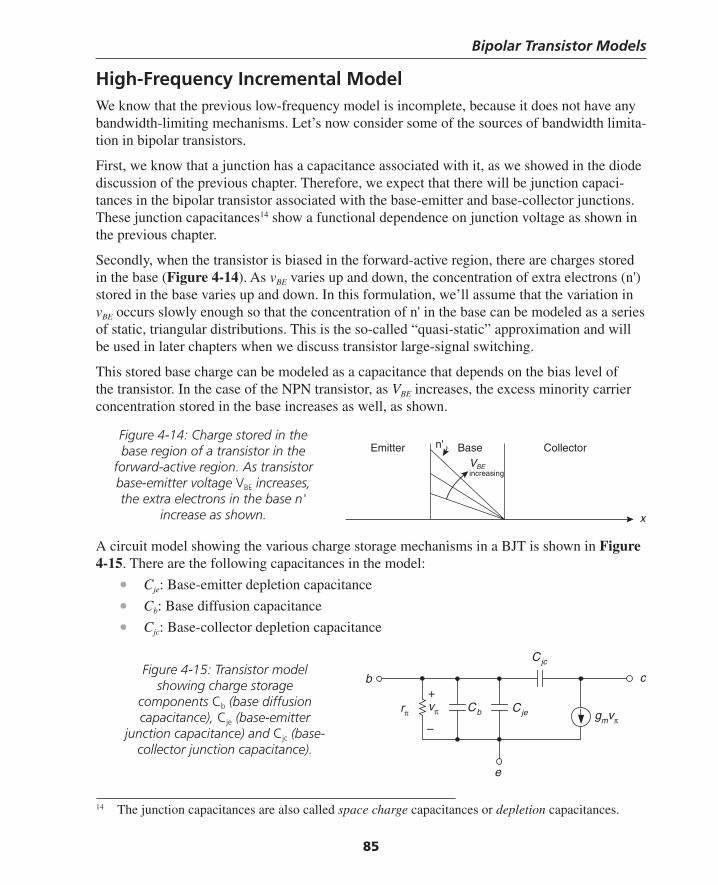
Bipolar Transistor Models
85
High-Frequency Incremental ModelWe know that the previous low-frequency model is incomplete, because it does not have any bandwidth-limiting mechanisms. Let’s now consider some of the sources of bandwidth limita-tion in bipolar transistors.
First, we know that a junction has a capacitance associated with it, as we showed in the diode discussion of the previous chapter. Therefore, we expect that there will be junction capaci-tances in the bipolar transistor associated with the base-emitter and base-collector junctions. These junction capacitances14 show a functional dependence on junction voltage as shown in the previous chapter.
Secondly, when the transistor is biased in the forward-active region, there are charges stored in the base (Figure 4-14). As vBE varies up and down, the concentration of extra electrons (n') stored in the base varies up and down. In this formulation, we’ll assume that the variation in vBE occurs slowly enough so that the concentration of n' in the base can be modeled as a series of static, triangular distributions. This is the so-called “quasi-static” approximation and will be used in later chapters when we discuss transistor large-signal switching.
This stored base charge can be modeled as a capacitance that depends on the bias level of the transistor. In the case of the NPN transistor, as VBE increases, the excess minority carrier concentration stored in the base increases as well, as shown.
Figure 4-14: Charge stored in the base region of a transistor in the
forward-active region. As transistor base-emitter voltage VBE increases, the extra electrons in the base n'
increase as shown.
14 The junction capacitances are also called space charge capacitances or depletion capacitances.
Emitter Base Collectorn'
VBEincreasing
x
A circuit model showing the various charge storage mechanisms in a BJT is shown in Figure 4-15. There are the following capacitances in the model:
• Cje: Base-emitter depletion capacitance
• Cb: Base diffusion capacitance
• Cjc: Base-collector depletion capacitance
Figure 4-15: Transistor model showing charge storage
components Cb (base diffusion capacitance), Cje (base-emitter
junction capacitance) and Cjc (base-collector junction capacitance).
+
–
b
rπ gmvπvπ
c
Cjc
Cb Cje
e
Thompson Book.indb 85 3/20/2006 11:34:16 AM
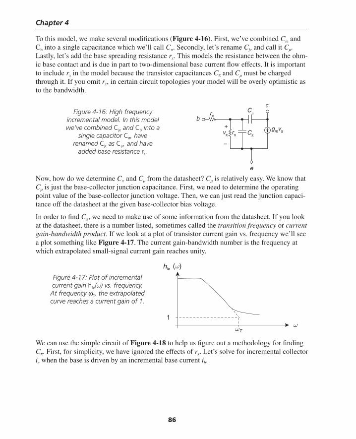
Chapter 4
86
To this model, we make several modifi cations (Figure 4-16). First, we’ve combined Cje and Cb into a single capacitance which we’ll call Cπ. Secondly, let’s rename Cjc and call it Cµ. Lastly, let’s add the base spreading resistance rx. This models the resistance between the ohm-ic base contact and is due in part to two-dimensional base current fl ow effects. It is important to include rx in the model because the transistor capacitances Cπ and Cµ must be charged through it. If you omit rx, in certain circuit topologies your model will be overly optimistic as to the bandwidth.
Figure 4-16: High frequency incremental model. In this model we’ve combined Cje and Cb into a
single capacitor Cπ, have renamed Cjc as Cµ, and have
added base resistance rx.
+
–
rxb
rπ Cπ
Cμ
e
gmvπvπ
c
Now, how do we determine Cπ and Cµ from the datasheet? Cµ is relatively easy. We know that Cµ is just the base-collector junction capacitance. First, we need to determine the operating point value of the base-collector junction voltage. Then, we can just read the junction capaci-tance off the datasheet at the given base-collector bias voltage.
In order to fi nd Cπ, we need to make use of some information from the datasheet. If you look at the datasheet, there is a number listed, sometimes called the transition frequency or current gain-bandwidth product. If we look at a plot of transistor current gain vs. frequency we’ll see a plot something like Figure 4-17. The current gain-bandwidth number is the frequency at which extrapolated small-signal current gain reaches unity.
Figure 4-17: Plot of incremental current gain hfe(ω) vs. frequency.
At frequency ωT, the extrapolated curve reaches a current gain of 1.
1ωωT
(ω)hfe
We can use the simple circuit of Figure 4-18 to help us fi gure out a methodology for fi nding Cπ. First, for simplicity, we have ignored the effects of rx. Let’s solve for incremental collector ic when the base is driven by an incremental base current ib.
Thompson Book.indb 86 3/20/2006 11:34:17 AM
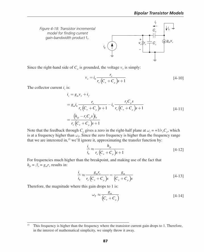
Bipolar Transistor Models
87
Figure 4-18: Transistor incremental model for fi nding current
gain-bandwidth product fT.
Since the right-hand side of Cμ is grounded, the voltage vπ is simply:
( ) 1b
rv i
r C C sπ
ππ π μ
=+ +
[4-10]
The collector current ic is:
( ) ( )( )( )
1 1
1
c m f
m b b
fe b
i g v i
r C srg i i
r C C s r C C s
h r C s i
r C C s
π
π μπ
π π μ π π μ
π μ
π π μ
= +
= −+ + + +
−=
+ +
[4-11]
Note that the feedback through Cμ gives a zero in the right-half plane at ωz = +1/rπCμ, which is at a frequency higher than ωT. Since the zero frequency is higher than the frequency range that we are interested in,15 we’ll ignore it, approximating the transfer function by:
( ) 1fec
b
hi
i r C C sπ π μ
≈+ +
[4-12]
For frequencies much higher than the breakpoint, and making use of the fact that hfe = βo = gmrπ results in:
( ) ( )c m m
b
i g r g
i r C C s C C sπ
π π μ π μ
≈ =+ + [4-13]
Therefore, the magnitude where this gain drops to 1 is:
( )m
T
g
C Cπ μ
ω ≈+ [4-14]
+
−
rπ Cπ
Cμ
gmvπvπib
ic
if
15 This frequency is higher than the frequency where the transistor current gain drops to 1. Therefore, in the interest of mathematical simplicity, we simply throw it away.
Thompson Book.indb 87 3/20/2006 11:34:17 AM
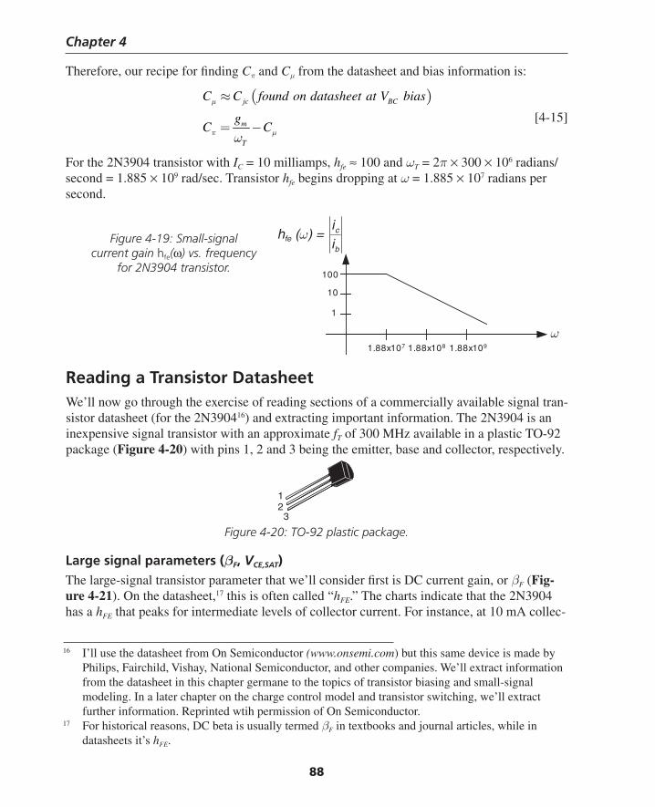
Chapter 4
88
Therefore, our recipe for fi nding Cπ and Cμ from the datasheet and bias information is:
( )jc BC
m
T
C C found on datasheet at V bias
gC C
μ
π μω
≈
= − [4-15]
For the 2N3904 transistor with IC = 10 milliamps, hfe ≈ 100 and ωT = 2π × 300 × 106 radians/second = 1.885 × 10⁹ rad/sec. Transistor hfe begins dropping at ω = 1.885 × 10⁷ radians per second.
Reading a Transistor DatasheetWe’ll now go through the exercise of reading sections of a commercially available signal tran-sistor datasheet (for the 2N390416) and extracting important information. The 2N3904 is an inexpensive signal transistor with an approximate fT of 300 MHz available in a plastic TO-92 package (Figure 4-20) with pins 1, 2 and 3 being the emitter, base and collector, respectively.
1
10
100
iic
b
ω1.88x1091.88x1081.88x107
hfe (ω) =Figure 4-19: Small-signal current gain hfe(ω) vs. frequency
for 2N3904 transistor.
Figure 4-20: TO-92 plastic package.
Large signal parameters (βF, VCE,SAT)The large-signal transistor parameter that we’ll consider fi rst is DC current gain, or βF (Fig-ure 4-21). On the datasheet,17 this is often called “hFE.” The charts indicate that the 2N3904 has a hFE that peaks for intermediate levels of collector current. For instance, at 10 mA collec-
321
16 I’ll use the datasheet from On Semiconductor (www.onsemi.com) but this same device is made by Philips, Fairchild, Vishay, National Semiconductor, and other companies. We’ll extract information from the datasheet in this chapter germane to the topics of transistor biasing and small-signal modeling. In a later chapter on the charge control model and transistor switching, we’ll extract further information. Reprinted wtih permission of On Semiconductor.
17 For historical reasons, DC beta is usually termed βF in textbooks and journal articles, while in datasheets it’s hFE.
Thompson Book.indb 88 3/20/2006 11:34:18 AM
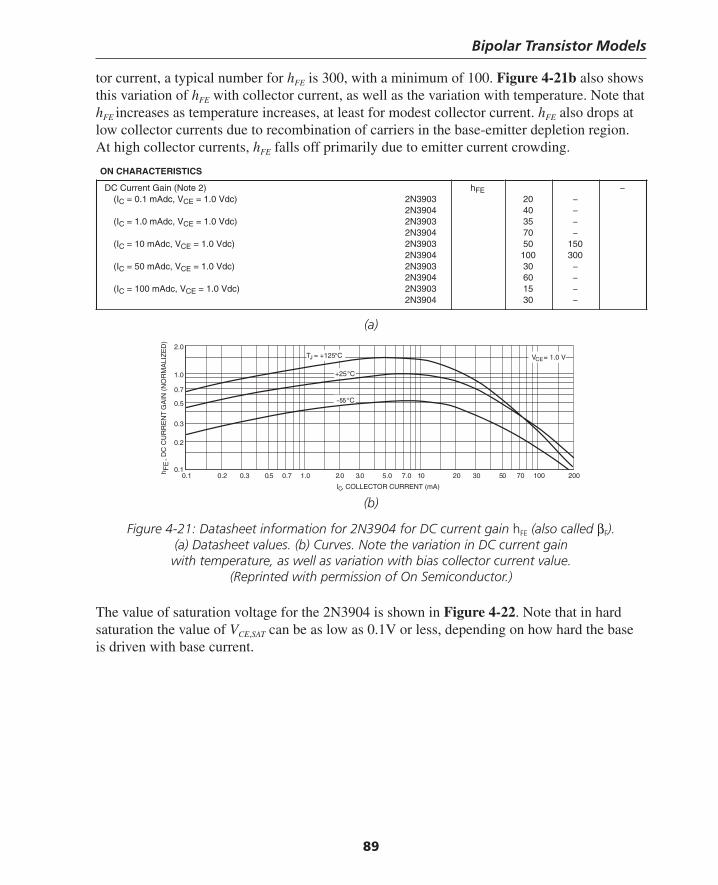
Bipolar Transistor Models
89
tor current, a typical number for hFE is 300, with a minimum of 100. Figure 4-21b also shows this variation of hFE with collector current, as well as the variation with temperature. Note that hFE increases as temperature increases, at least for modest collector current. hFE also drops at low collector currents due to recombination of carriers in the base-emitter depletion region. At high collector currents, hFE falls off primarily due to emitter current crowding.
(a)
ON CHARACTERISTICS
DC Current Gain (Note 2)(IC = 0.1 mAdc, VCE 3093N2)cdV 0.1 =
2N3904(IC = 1.0 mAdc, VCE 3093N2)cdV 0.1 =
2N3904(IC = 10 mAdc, VCE 3093N2)cdV 0.1 =
2N3904(IC = 50 mAdc, VCE 3093N2)cdV 0.1 =
2N3904(IC = 100 mAdc, VCE 3093N2)cdV 0.1 =
2N3904
hFE204035705010030601530
−−−−
150300−−−−
−
(b)
Figure 4-21: Datasheet information for 2N3904 for DC current gain hFE (also called βF). (a) Datasheet values. (b) Curves. Note the variation in DC current gain with temperature, as well as variation with bias collector current value.
(Reprinted with permission of On Semiconductor.)
The value of saturation voltage for the 2N3904 is shown in Figure 4-22. Note that in hard saturation the value of VCE,SAT can be as low as 0.1V or less, depending on how hard the base is driven with base current.
IC, COLLECTOR CURRENT (mA)
0.3
0.5
0.7
1.0
2.0
0.2
0.1h
, D
C C
UR
RE
NT
GA
IN (
NO
RM
ALI
ZE
D)
05010.30.25.0 700.2 0.30.1
1001.00.7 20030205.0 7.0
FE
VCE = 1.0 VTJ = +125°C
+25°C
°C
Thompson Book.indb 89 3/20/2006 11:34:18 AM
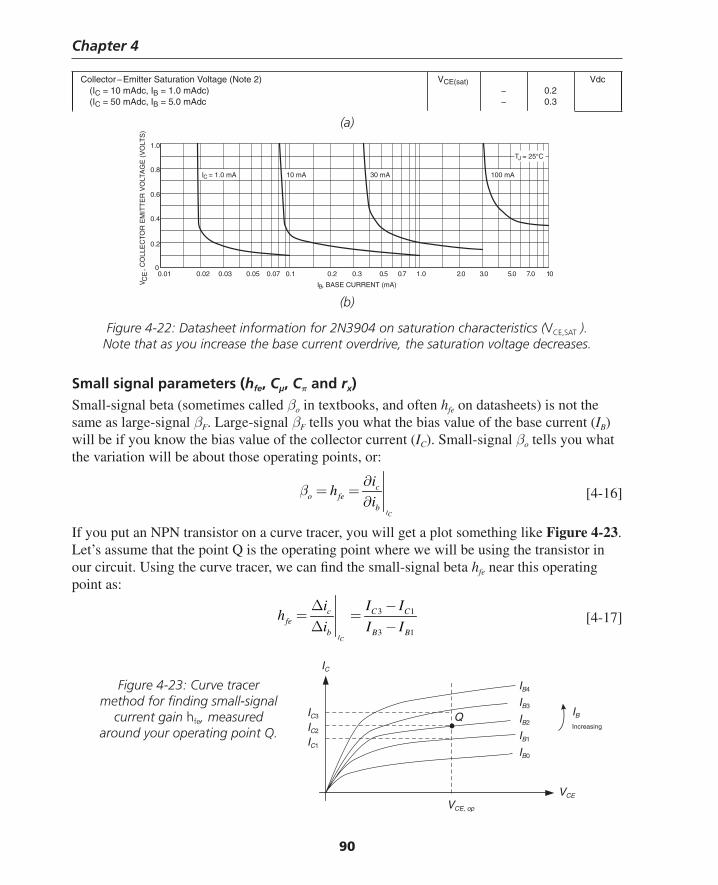
Chapter 4
90
(a)
Collector−Emitter Saturation Voltage (Note 2)(IC = 10 mAdc, IB = 1.0 mAdc)(IC = 50 mAdc, IB = 5.0 mAdc
VCE(sat)−−
0.20.3
Vdc
(b)
Figure 4-22: Datasheet information for 2N3904 on saturation characteristics (VCE,SAT ). Note that as you increase the base current overdrive, the saturation voltage decreases.
Small signal parameters (hfe, Cµ, Cπ and rx)Small-signal beta (sometimes called βo in textbooks, and often hfe on datasheets) is not the same as large-signal βF. Large-signal βF tells you what the bias value of the base current (IB) will be if you know the bias value of the collector current (IC). Small-signal βo tells you what the variation will be about those operating points, or:
IC
co fe
b
ih
iβ
∂= =
∂ [4-16]
If you put an NPN transistor on a curve tracer, you will get a plot something like Figure 4-23. Let’s assume that the point Q is the operating point where we will be using the transistor in our circuit. Using the curve tracer, we can fi nd the small-signal beta hfe near this operating point as:
3 1
3 1IC
c C Cfe
b B B
i I Ih
i I I
Δ −= =
Δ − [4-17]
IB, BASE CURRENT (mA)
0.4
0.6
0.8
1.0
0.2
0.1
V
, C
OLL
EC
TOR
EM
ITT
ER
VO
LTA
GE
(V
OLT
S)
010.30.25.00.2 0.30
1.0 0.70.57.0
CE
IC = 1.0 mA
TJ = 25°C
0.070.050.030.020.01
10 mA 30 mA 100 mA
VCE
VCE, op
IC3
IC2
IC1
IB4
IB3
IB2
IB1
IB0
IB
IncreasingQ
IC
Figure 4-23: Curve tracer method for fi nding small-signal
current gain hfe, measured around your operating point Q.
Thompson Book.indb 90 3/20/2006 11:34:19 AM
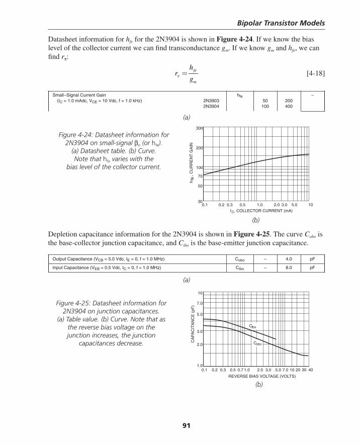
Bipolar Transistor Models
91
Datasheet information for hfe for the 2N3904 is shown in Figure 4-24. If we know the bias level of the collector current we can fi nd transconductance gm. If we know gm and hfe, we can fi nd rπ:
fe
m
hr
gπ = [4-18]
(a)
(b)
Small−Signal Current Gain(IC = 1.0 mAdc, VCE 3093N2)zHk 0.1 = f ,cdV 01 =
2N3904
hfe50100
200400
−
IC, COLLECTOR CURRENT (mA)
70
100
200
300
50h
, C
UR
RE
NT
GA
IN
300.1 0.2 1.0 2.0 5.0 100.3 0.5 3.0
fe
Depletion capacitance information for the 2N3904 is shown in Figure 4-25. The curve Cobo is the base-collector junction capacitance, and Cibo is the base-emitter junction capacitance.
Output Capacitance (VCB = 5.0 Vdc, IE = 0, f = 1.0 MHz) Cobo − 4.0 pF
Input Capacitance (VEB = 0.5 Vdc, IC = 0, f = 1.0 MHz) Cibo − 8.0 pF
(a)
REVERSE BIAS VOLTAGE (VOLTS)
2.0
3.0
5.0
7.0
10
1.00.1
CA
PA
CIT
AN
CE
(pF
)
1.0 2.0 3.0 5.0 7.0 10 20 30 400.2 0.3 0.5 0.7
Cibo
Cobo
Figure 4-24: Datasheet information for 2N3904 on small-signal βo (or hfe).
(a) Datasheet table. (b) Curve. Note that hfe varies with the
bias level of the collector current.
(b)
Figure 4-25: Datasheet information for 2N3904 on junction capacitances.
(a) Table value. (b) Curve. Note that as the reverse bias voltage on the junction increases, the junction
capacitances decrease.
Thompson Book.indb 91 3/20/2006 11:34:20 AM
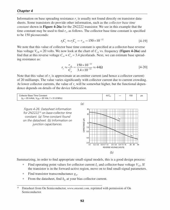
Chapter 4
92
Information on base spreading resistance rx is usually not found directly on transistor data-sheets. Some transistors do provide other information, such as the collector base time constant shown in Figure 4-26a for the 2N2222 transistor. We see in this example that the time constant may be used to fi nd rx, as follows. The collector base time constant is specifi ed to be 150 picoseconds:
12150 10b c x cbr C r Cμ τ −≈ = = × [4-19]
We note that this value of collector base time constant is specifi ed at a collector-base reverse bias voltage VCB = 20 volts. We now look at the chart of Ccb vs. frequency (Figure 4-26a) and fi nd that at this reverse voltage Ccb = Cμ ≈ 3.4 picofarads. Next, we can estimate base spread-ing resistance as:
12
12
150 1044
3.4 10cb
xr Cμ
τ −
−
×≈ = ≈
×Ω [4-20]
Note that this value of rx is approximate at an emitter current (and hence a collector current) of 20 milliamps. The value varies signifi cantly with collector current due to current crowding. At lower collector currents, the value of rx will be somewhat higher, but the functional depen-dence depends on details of the device fabrication.
(a)
Summarizing, in order to fi nd appropriate small-signal models, this is a good design process:
• Find operating point values for collector current IC and collector-base voltage VCE. If the transistor is in the forward-active region, move on to fi nd small-signal parameters.
• Find transistor transconductance gm.
• From the datasheet, fi nd hfe at your bias collector current.
Collector Base Time Constant(IE = 20 mAdc, VCB = 20 Vdc, f = 31.8 MHz)
rb′Cc — 150 ps
(b)
Figure 4-26: Datasheet information for 2N222218 on base-collector time constant. (a) Time constant found
on the datasheet. (b) Information on junction capacitances.
18 Datasheet from On Semiconductor, www.onsemi.com, reprinted with permission of On Semiconductor.
Thompson Book.indb 92 3/20/2006 11:34:20 AM
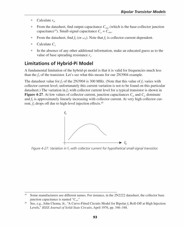
Bipolar Transistor Models
93
• Calculate rπ.
• From the datasheet, fi nd output capacitance Cobo (which is the base-collector junction capacitance19). Small-signal capacitance Cμ = Cobo.
• From the datasheet, fi nd fT (or ωT). Note that fT is collector-current-dependent.
• Calculate Cπ.
• In the absence of any other additional information, make an educated guess as to the value of base spreading resistance rx.
Limitations of Hybrid-Pi ModelA fundamental limitation of the hybrid-pi model is that it is valid for frequencies much less than the fT of the transistor. Let’s see what this means for our 2N3904 example.
The datasheet value for fT of the 2N3904 is 300 MHz. (Note that this value of fT varies with collector current level; unfortunately this current variation is not to be found on this particular datasheet.) The variation in fT with collector current level for a typical transistor is shown in Figure 4-27. At low values of collector current, junction capacitances Cje and Cjc dominate and fT is approximately linearly increasing with collector current. At very high collector cur-rent, fT drops off due to high-level injection effects.20
19 Some manufacturers use different names. For instance, in the 2N2222 datasheet, the collector base junction capacitance is named “Ccb.”
20 See, e.g., John Choma, Jr., “A Curve-Fitted Circuits Model for Bipolar fT Roll-Off at High Injection Levels,” IEEE Journal of Solid-State Circuits, April 1976, pp. 346–348.
Figure 4-27: Variation in fT with collector current for hypothetical small-signal transistor.
IC
fT
Thompson Book.indb 93 3/20/2006 11:34:21 AM
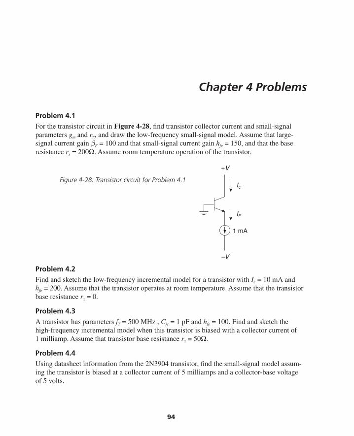
94
Chapter 4 Problems
Problem 4.1 For the transistor circuit in Figure 4-28, fi nd transistor collector current and small-signal parameters gm and rπ, and draw the low-frequency small-signal model. Assume that large-signal current gain βF = 100 and that small-signal current gain hfe = 150, and that the base resistance rx = 200Ω. Assume room temperature operation of the transistor.
Figure 4-28: Transistor circuit for Problem 4.1
Problem 4.2Find and sketch the low-frequency incremental model for a transistor with Ic = 10 mA and hfe = 200. Assume that the transistor operates at room temperature. Assume that the transistor base resistance rx = 0.
Problem 4.3A transistor has parameters fT = 500 MHz , Cjc = 1 pF and hfe = 100. Find and sketch the high-frequency incremental model when this transistor is biased with a collector current of 1 milliamp. Assume that transistor base resistance rx = 50Ω.
Problem 4.4Using datasheet information from the 2N3904 transistor, fi nd the small-signal model assum-ing the transistor is biased at a collector current of 5 milliamps and a collector-base voltage of 5 volts.
IC
IE
+V
–V
1 mA
Thompson Book.indb 94 3/20/2006 11:34:21 AM
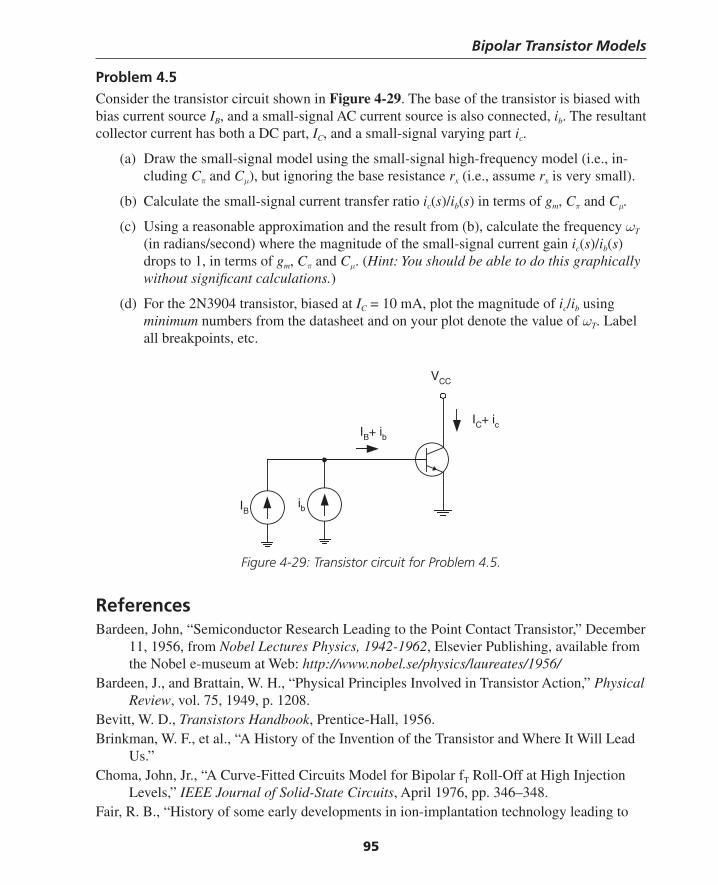
Bipolar Transistor Models
95
Problem 4.5Consider the transistor circuit shown in Figure 4-29. The base of the transistor is biased with bias current source IB, and a small-signal AC current source is also connected, ib. The resultant collector current has both a DC part, IC, and a small-signal varying part ic.
(a) Draw the small-signal model using the small-signal high-frequency model (i.e., in-cluding Cπ and Cμ), but ignoring the base resistance rx (i.e., assume rx is very small).
(b) Calculate the small-signal current transfer ratio ic(s)/ib(s) in terms of gm, Cπ and Cμ.
(c) Using a reasonable approximation and the result from (b), calculate the frequency ωT (in radians/second) where the magnitude of the small-signal current gain ic(s)/ib(s) drops to 1, in terms of gm, Cπ and Cμ. (Hint: You should be able to do this graphically without signifi cant calculations.)
(d) For the 2N3904 transistor, biased at IC = 10 mA, plot the magnitude of ic/ib using minimum numbers from the datasheet and on your plot denote the value of ωT. Label all breakpoints, etc.
Figure 4-29: Transistor circuit for Problem 4.5.
ReferencesBardeen, John, “Semiconductor Research Leading to the Point Contact Transistor,” December
11, 1956, from Nobel Lectures Physics, 1942-1962, Elsevier Publishing, available from the Nobel e-museum at Web: http://www.nobel.se/physics/laureates/1956/
Bardeen, J., and Brattain, W. H., “Physical Principles Involved in Transistor Action,” Physical Review, vol. 75, 1949, p. 1208.
Bevitt, W. D., Transistors Handbook, Prentice-Hall, 1956.Brinkman, W. F., et al., “A History of the Invention of the Transistor and Where It Will Lead
Us.”Choma, John, Jr., “A Curve-Fitted Circuits Model for Bipolar fT Roll-Off at High Injection
Levels,” IEEE Journal of Solid-State Circuits, April 1976, pp. 346–348.Fair, R. B., “History of some early developments in ion-implantation technology leading to
IB ib
IB+ ibIC+ ic
VCC
Thompson Book.indb 95 3/20/2006 11:34:22 AM
Chapter 4
96
silicon transistor manufacturing,” Proceedings of the IEEE, vol. 86, no. 1, January 1998, pp. 111–137.
Gough, Russell, “High-Frequency Transistor Modeling for Circuit Simulation,” IEEE Journal of Solid-State Circuits, vol. SC-17, no. 4, August 1982, pp. 666–670.
Gray, P. E., DeWitt, D., Boothroyd, A. R., and Gibbons, J. F., Physical Electronics and Cir-cuit Models of Transistors, Semiconductor Electronics Education Committee, volume 2, John Wiley, 1964.
Gray, Paul E., and Searle, Campbell L., Electronic Principles: Physics, Models and Circuits, John Wiley, 1969.
Gray, Paul R. and Meyer, Robert G., Analysis and Design of Analog Integrated Circuits, 2d edition, John Wiley, 1984.
Greeneich, E. W., “An Appropriate Device Figure of Merit for Bipolar CML,” IEEE Electron Device Letters, vol. 12, 1991, p. 18.
Hurkx, G. A. M., “The Relevance of fT and fmax for the Speed of a Bipolar CE Amplifi er Stage,” IEEE Transactions on Electron Devices, vol. 44, no. 5, May 1997, pp. 775–781.
Lo, A. W., Endres, R., Zawels, J., Waldhauer, F., and Cheng, C., Transistor Electronics, Prentice-Hall, 1955.
Muller, Richard S., and Kamins, Theodore I., Device Electronics for Integrated Circuits, 2d edition, John Wiley, 1986.
Neudeck, Gerold W., Modular Series on Solid State Devices, The Bipolar Junction Transistor, Addison-Wesley, 1983.
On Semiconductor website: http://www.onsemi.com Pritchard, R. L., “Transistor equivalent circuits,” Proceedings of the IEEE, vol. 86, no. 1,
January 1998, pp. 150–162.Sansen, Willy, and Meyer, Robert, “Characterization and Measurement of the Base and
Emitter Resistances of Bipolar Transistors,” IEEE Journal of Solid-State Circuits, vol. SC-7, no. 6, December 1972, pp. 492–498.
Searle, C. L., Boothroyd, A. R., Angelo, E. J., Jr., Gray, P. E., and Pederson, D. O., Elementary Circuit Properties of Transistors, Semiconductor Electronics Education Committee, volume 3, John Wiley, 1964.
Shockley, William, “Transistor Technology Evokes New Physics,” December 11, 1956, from Nobel Lectures Physics, 1942–1962, Elsevier Publishing, available from the Nobel e-museum at Web: http://www.nobel.se/physics/laureates/1956/
Sze, S. M., Physics of Semiconductor Devices, 2d edition, John Wiley, 1981.Warner, Raymond M., “Microelectronics: Its Unusual Origin and Personality,” IEEE Transac-
tions on Electron Devices, vol. 48, no. 11, November 2001, pp. 2457–2467.
Thompson Book.indb 96 3/20/2006 11:34:22 AM
97
C H A P T E R 5Basic Bipolar Transistor Amplifi ers and Biasing
The Issue of Transistor BiasingIn order to achieve useful amplifi cation from a transistor, the transistor is generally biased in the forward-active region (FAR). The FAR is the region of operation of the transistor where amplifi cation can occur because the transistor provides current gain. Biasing is the process by which one sets the DC operating point of a transistor amplifi er to a known and repeatable point in this forward-active region. If you do your biasing correctly, your amplifi er output bias level will not drift signifi cantly with time, temperature or component variations.
Let’s consider the simple bias circuit shown in Figure 5-1a. The bias voltage VBB = 5V sets the base current as follows:
IV V
RBBB BE
B
=−
≈−
≈5 0 7
28 6150
.
. kA
Ωμ [5-1]
This initial calculation assumes that the base-emitter voltage VBE = 0.7V, which is approxi-mately correct if the transistor is biased in the forward-active region and the base-emitter junction is forward biased. Let’s assume that this transistor has a DC current gain βF = 175. This means that the collector current is:
I IV V
RC F B FBB BE
B
= =−⎛
⎝⎜⎜⎜⎜
⎞
⎠⎟⎟⎟⎟
≈ × ≈β β 175 150 26 25μA milliamps. [5-2]
With a load resistor RL = 240Ω, there is a 6.3V drop across this load resistor and hence VCE = 5.7V. The operating point, labeled Q for quiescent operating point, is shown in Figure 5-1b. The operating point is the intersection of the transistor characteristic curves with the load line imposed by the 240Ω resistor.
In This Chapter
In this chapter, we cover some basic transistor topologies, including the common-emitter amplifi er, emitter-follower, common-base and differential amplifi ers. The important issue of biasing—connection of the transistor so that it operates in the forward-active region—is also discussed in detail.
Thompson Book.indb 97 3/20/2006 11:34:22 AM
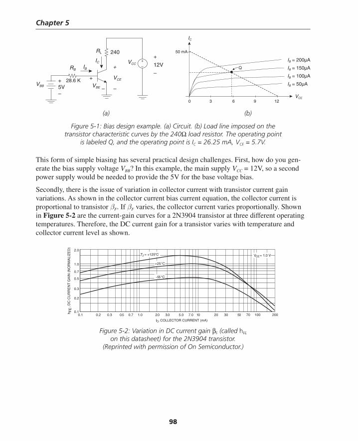
Chapter 5
98
IC
IB
VBB+5V–
RL 240
VCC+
VCE
–
+
12V
–
VBE
RB
28.6 K +
–
(a) (b)
Figure 5-1: Bias design example. (a) Circuit. (b) Load line imposed on the transistor characteristic curves by the 240Ω load resistor. The operating point
is labeled Q, and the operating point is IC = 26.25 mA, VCE = 5.7V.
This form of simple biasing has several practical design challenges. First, how do you gen-erate the bias supply voltage VBB? In this example, the main supply VCC = 12V, so a second power supply would be needed to provide the 5V for the base voltage bias.
Secondly, there is the issue of variation in collector current with transistor current gain variations. As shown in the collector current bias current equation, the collector current is proportional to transistor βF. If βF varies, the collector current varies proportionally. Shown in Figure 5-2 are the current-gain curves for a 2N3904 transistor at three different operating temperatures. Therefore, the DC current gain for a transistor varies with temperature and collector current level as shown.
VCE
Q
IC
50 mA
IB = 200µA
IB = 150µA
IB = 100µA
IB = 50µA
0 3 6 9 12
Figure 5-2: Variation in DC current gain βF (called hFE on this datasheet) for the 2N3904 transistor.
(Reprinted with permission of On Semiconductor.)
IC, COLLECTOR CURRENT (mA)
0.3
0.5
0.7
1.0
2.0
0.2
0.1h
, D
C C
UR
RE
NT
GA
IN (
NO
RM
ALI
ZE
D)
05010.30.25.0 700.2 0.30.1
1001.00.7 20030205.0 7.0
FE
VCE = 1.0 VTJ = +125°C
+25°C
°C
Thompson Book.indb 98 3/20/2006 11:34:23 AM
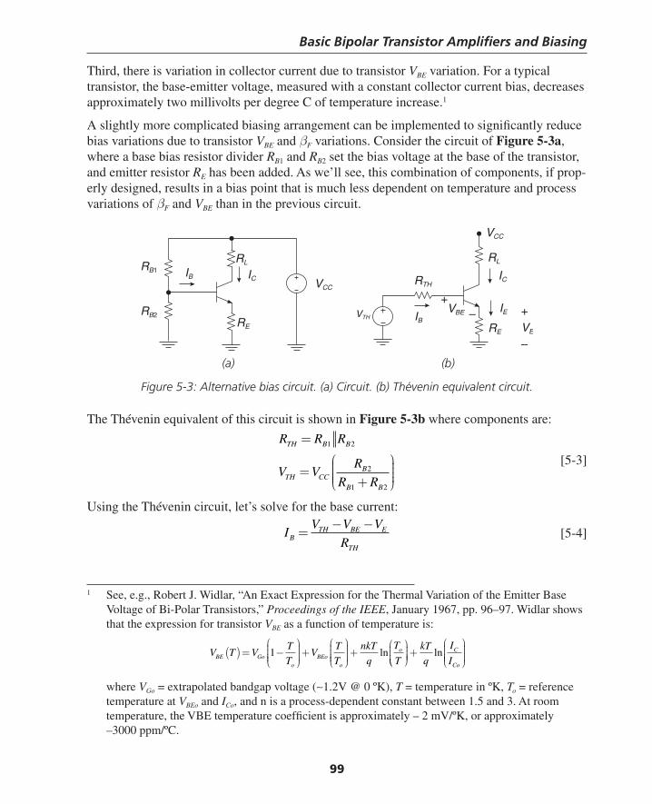
Basic Bipolar Transistor Amplifi ers and Biasing
99
Third, there is variation in collector current due to transistor VBE variation. For a typical transistor, the base-emitter voltage, measured with a constant collector current bias, decreases approximately two millivolts per degree C of temperature increase.1
A slightly more complicated biasing arrangement can be implemented to signifi cantly reduce bias variations due to transistor VBE and βF variations. Consider the circuit of Figure 5-3a, where a base bias resistor divider RB1 and RB2 set the bias voltage at the base of the transistor, and emitter resistor RE has been added. As we’ll see, this combination of components, if prop-erly designed, results in a bias point that is much less dependent on temperature and process variations of βF and VBE than in the previous circuit.
1 See, e.g., Robert J. Widlar, “An Exact Expression for the Thermal Variation of the Emitter Base Voltage of Bi-Polar Transistors,” Proceedings of the IEEE, January 1967, pp. 96–97. Widlar shows that the expression for transistor VBE as a function of temperature is:
V T VT
TV
T
T
nkT
q
T
TBE Goo
BEoo
o( )= −⎛
⎝⎜⎜⎜⎜
⎞
⎠⎟⎟⎟⎟+
⎛
⎝⎜⎜⎜⎜
⎞
⎠⎟⎟⎟⎟+
⎛1 ln
⎝⎝⎜⎜⎜
⎞
⎠⎟⎟⎟⎟+
⎛
⎝⎜⎜⎜⎜
⎞
⎠⎟⎟⎟⎟
kT
q
I
IC
Co
ln
where VGo = extrapolated bandgap voltage (∼1.2V @ 0 ºK), T = temperature in ºK, To = reference temperature at VBEo and ICo, and n is a process-dependent constant between 1.5 and 3. At room temperature, the VBE temperature coeffi cient is approximately – 2 mV/ºK, or approximately –3000 ppm/ºC.
(a) (b)
Figure 5-3: Alternative bias circuit. (a) Circuit. (b) Thévenin equivalent circuit.
The Thévenin equivalent of this circuit is shown in Figure 5-3b where components are:
R R R
V VR
R R
TH B B
TH CCB
B B
=
=+
⎛
⎝⎜⎜⎜⎜
⎞
⎠⎟⎟⎟⎟
1 2
2
1 2
[5-3]
Using the Thévenin circuit, let’s solve for the base current:
IV V V
RBTH BE E
TH
=− −
[5-4]
ICIB
RL
VTH
VCC
+VE
–
VBE
RB1
RB2
+–
RE
RL
IB
IC
IE
RE
VCC
RTH
Thompson Book.indb 99 3/20/2006 11:34:24 AM
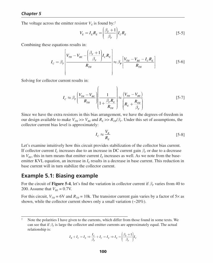
Chapter 5
100
The voltage across the emitter resistor VE is found by:2
V I R I RE E EF
FC E= =
+⎛
⎝⎜⎜⎜⎜
⎞
⎠⎟⎟⎟⎟
ββ
1 [5-5]
Combining these equations results in:
I
V V I R
RC F
TH BEF
FC E
TH
=− −
+⎛
⎝⎜⎜⎜⎜
⎞
⎠⎟⎟⎟⎟
⎡
⎣
⎢⎢⎢⎢⎢⎢⎢
⎤
⎦
⎥⎥⎥⎥⎥⎥⎥
≈β
ββ
β
1
FFTH BE C E
TH
V V I R
R
− −⎡
⎣⎢⎢
⎤
⎦⎥⎥ [5-6]
Solving for collector current results in:
IV V
R R
R
C FTH BE
TH F E
TH
≈−⎛
⎝⎜⎜⎜⎜
⎞
⎠⎟⎟⎟⎟
+
⎛
⎝
⎜⎜⎜⎜⎜⎜⎜⎜⎜⎜
⎞
⎠
⎟⎟⎟⎟⎟⎟⎟ββ1
1 ⎟⎟⎟⎟⎟
≈−( )
+⎛
⎝⎜⎜⎜⎜
⎞
⎠⎟⎟⎟⎟
V V
RR
TH BE
ETH
Fβ
[5-7]
Since we have the extra resistors in this bias arrangement, we have the degrees-of-freedom in our design available to make VTH >> VBE and RE >> RTH/βF. Under this set of assumptions, the collector current bias level is approximately:
IV
RCB
E
≈ [5-8]
Let’s examine intuitively how this circuit provides stabilization of the collector bias current. If collector current IC increases due to an increase in DC current gain βF or due to a decrease in VBE, this in turn means that emitter current IE increases as well. As we note from the base-emitter KVL equation, an increase in IE results in a decrease in base current. This reduction in base current will in turn stabilize the collector current.
Example 5.1: Biasing exampleFor the circuit of Figure 5-4, let’s fi nd the variation in collector current if βF varies from 40 to 200. Assume that VBE = 0.7V.
For this circuit, VTH = 6V and RTH = 10k. The transistor current gain varies by a factor of 5× as shown, while the collector current shows only a small variation (~20%).
2 Note the polarities I have given to the currents, which differ from those found in some texts. We can see that if βF is large the collector and emitter currents are approximately equal. The actual relationship is:
I I II
I I I IB C EC
FC E E
F
FC+ = ⇒ + = ⇒ =
+⎛
⎝⎜⎜⎜⎜
⎞
⎠⎟⎟⎟⎟β
ββ
1
Thompson Book.indb 100 3/20/2006 11:34:24 AM
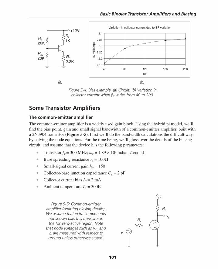
Basic Bipolar Transistor Amplifi ers and Biasing
101
(a) (b)
Figure 5-4: Bias example. (a) Circuit. (b) Variation in collector current when βF varies from 40 to 200.
Some Transistor Amplifi ers
The common-emitter amplifi erThe common-emitter amplifi er is a widely used gain block. Using the hybrid pi model, we’ll fi nd the bias point, gain and small signal bandwidth of a common-emitter amplifi er, built with a 2N3904 transistor (Figure 5-5). First we’ll do the bandwidth calculations the diffi cult way, by solving the node equations. For the time being, we’ll gloss over the details of the biasing circuit, and assume that the device has the following parameters:
• Transistor fT = 300 MHz; ωT = 1.89 × 10⁹ radians/second
• Base spreading resistance rx = 100Ω• Small-signal current gain hfe = 150
• Collector-base junction capacitance Cμ = 2 pF
• Collector current bias IC = 2 mA
• Ambient temperature TA = 300K
RB1
20K
RB2
20K RE
2.2K
RL
1K
+12VVariation in collector current due to BF variation
2.15
2.2
2.25
2.3
2.35
2.4
40 80 120 160 200
BF
Ic, m
illia
mps
VCC
vi
voRs
RL
Figure 5-5: Common-emitter amplifi er (omitting biasing details). We assume that extra components
not shown bias this transistor in the forward-active region. Note
that node voltages such as VCC and vo are measured with respect to ground unless otherwise stated.
Thompson Book.indb 101 3/20/2006 11:34:25 AM
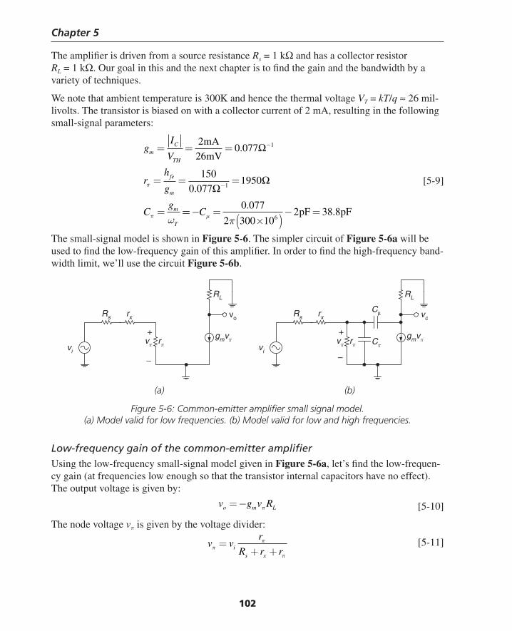
Chapter 5
102
The amplifi er is driven from a source resistance Rs = 1 kΩ and has a collector resistor RL = 1 kΩ. Our goal in this and the next chapter is to fi nd the gain and the bandwidth by a variety of techniques.
We note that ambient temperature is 300K and hence the thermal voltage VT = kT/q ≈ 26 mil-livolts. The transistor is biased on with a collector current of 2 mA, resulting in the following small-signal parameters:
gI
V
rh
g
Cg
mC
TH
fe
m
m
T
= = =
= = =
=
−
−
2
260 077
150
0 0771950
1
1
mA
mV.
.
Ω
ΩΩπ
π ω== − =
×( )− =Cμ π
0 077
2 300 102 38 8
6
..pF pF
[5-9]
The small-signal model is shown in Figure 5-6. The simpler circuit of Figure 5-6a will be used to fi nd the low-frequency gain of this amplifi er. In order to fi nd the high-frequency band-width limit, we’ll use the circuit Figure 5-6b.
(a) (b)
Figure 5-6: Common-emitter amplifi er small signal model. (a) Model valid for low frequencies. (b) Model valid for low and high frequencies.
Low-frequency gain of the common-emitter amplifi erUsing the low-frequency small-signal model given in Figure 5-6a, let’s fi nd the low-frequen-cy gain (at frequencies low enough so that the transistor internal capacitors have no effect). The output voltage is given by:
v g v Ro m L= − π [5-10]
The node voltage vπ is given by the voltage divider:
v vr
R r ris x
ππ
π
=+ +
[5-11]
+
_
rx
rπgmvπvπ
vo
RL
Rs
vi
+
–
rx
rπ Cπ
Cμ
gmvπvπ
vo
RL
Rs
vi
Thompson Book.indb 102 3/20/2006 11:34:25 AM
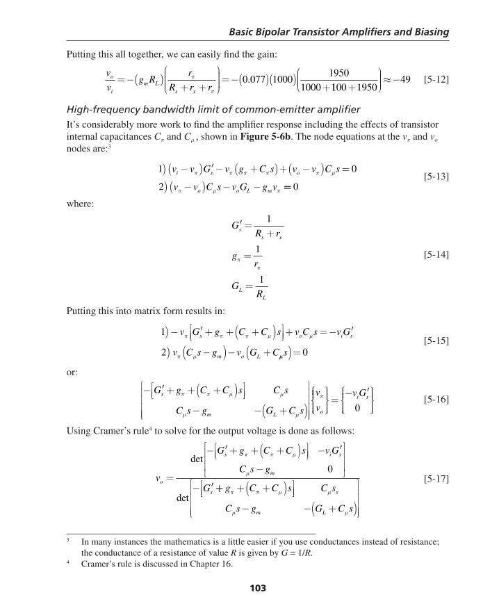
Basic Bipolar Transistor Amplifi ers and Biasing
103
Putting this all together, we can easily fi nd the gain:
v
vg R
r
R r ro
im L
s x
= −( )+ +
⎛
⎝⎜⎜⎜⎜
⎞
⎠⎟⎟⎟⎟
= −( )( )+
π
π
0 077 10001950
1000.
1100 195049
+
⎛⎝⎜⎜⎜
⎞⎠⎟⎟⎟ ≈ − [5-12]
High-frequency bandwidth limit of common-emitter amplifi erIt’s considerably more work to fi nd the amplifi er response including the effects of transistor internal capacitances Cπ and Cμ , shown in Figure 5-6b. The node equations at the vπ and vo nodes are:3
1 0
2
) −( ) ′ − +( )+ −( ) =
) −( ) − −
v v G v g C s v v C s
v v C s v G g v
i s o
o o L m
π π π π π μ
π μ π == 0 [5-13]
where:
′ =+
=
=
GR r
gr
GR
ss x
LL
1
1
1
ππ
[5-14]
Putting this into matrix form results in:
1
2
) − ′ + + +( )⎡⎣⎢
⎤⎦⎥ + = − ′
) −( )− +
v G g C C s v C s v G
v C s g v G C
s o i s
m o L
π π π μ μ
π μ μμs( )= 0 [5-15]
or:
− ′ + + +( )⎡
⎣⎢⎤⎦⎥
− − +( )
⎡
⎣
⎢⎢⎢⎢
⎤
⎦
⎥⎥⎥⎥
⎧⎨
G g C C s C s
C s g G C s
v
v
s
m L o
π π μ μ
μ μ
π⎪⎪⎪⎩⎪⎪
⎫⎬⎪⎪⎭⎪⎪
=− ′⎧
⎨⎪⎪⎩⎪⎪
⎫⎬⎪⎪⎭⎪⎪
v Gi s
0 [5-16]
Using Cramer’s rule4 to solve for the output voltage is done as follows:
v
G g C C s v G
C s g
Go
s i s
m
s
=
− ′ + + +( )⎡⎣⎢
⎤⎦⎥ − ′
−
⎡
⎣
⎢⎢⎢
⎤
⎦
⎥⎥⎥
− ′
det
det
π π μ
μ 0
++ + +( )⎡⎣⎢
⎤⎦⎥
− − +( )
⎡
⎣
⎢⎢⎢⎢
⎤
⎦
⎥⎥⎥⎥
g C C s C s
C s g G C s
s
m L
π π μ μ
μ μ
[5-17]
3 In many instances the mathematics is a little easier if you use conductances instead of resistance; the conductance of a resistance of value R is given by G = 1/R.
4 Cramer’s rule is discussed in Chapter 16.
Thompson Book.indb 103 3/20/2006 11:34:26 AM
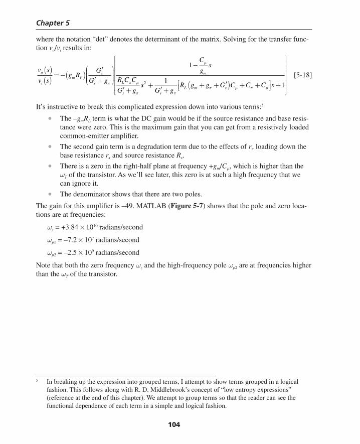
Chapter 5
104
where the notation “det” denotes the determinant of the matrix. Solving for the transfer func-tion vo/vi results in:
v s
v sg R
G
G g
C
gs
R C C
G g
o
im L
s
s
m
L
s
( )( )
= −( )′
′ +
⎛
⎝⎜⎜⎜⎜
⎞
⎠⎟⎟⎟⎟
−
′ +π
μ
π μ
π
1
ssG g
R g g G C C C ss
L m s2 1
1+′ +
+ + ′( ) + +⎡⎣⎢
⎤⎦⎥ +
⎡
⎣
⎢⎢⎢⎢⎢⎢
⎤
⎦
⎥⎥⎥⎥⎥⎥
ππ μ π μ
[5-18]
It’s instructive to break this complicated expression down into various terms:5
• The –gmRL term is what the DC gain would be if the source resistance and base resis-tance were zero. This is the maximum gain that you can get from a resistively loaded common-emitter amplifi er.
• The second gain term is a degradation term due to the effects of rπ loading down the base resistance rx and source resistance Rs.
• There is a zero in the right-half plane at frequency +gm/Cμ, which is higher than the ωT of the transistor. As we’ll see later, this zero is at such a high frequency that we can ignore it.
• The denominator shows that there are two poles.
The gain for this amplifi er is –49. MATLAB (Figure 5-7) shows that the pole and zero loca-tions are at frequencies:
ωz = +3.84 × 10¹⁰ radians/second
ωp1 = –7.2 × 10⁷ radians/second
ωp2 = –2.5 × 10⁹ radians/second
Note that both the zero frequency ωz and the high-frequency pole ωp2 are at frequencies higher than the ωT of the transistor.
5 In breaking up the expression into grouped terms, I attempt to show terms grouped in a logical fashion. This follows along with R. D. Middlebrook’s concept of “low entropy expressions” (reference at the end of this chapter). We attempt to group terms so that the reader can see the functional dependence of each term in a simple and logical fashion.
Thompson Book.indb 104 3/20/2006 11:34:26 AM
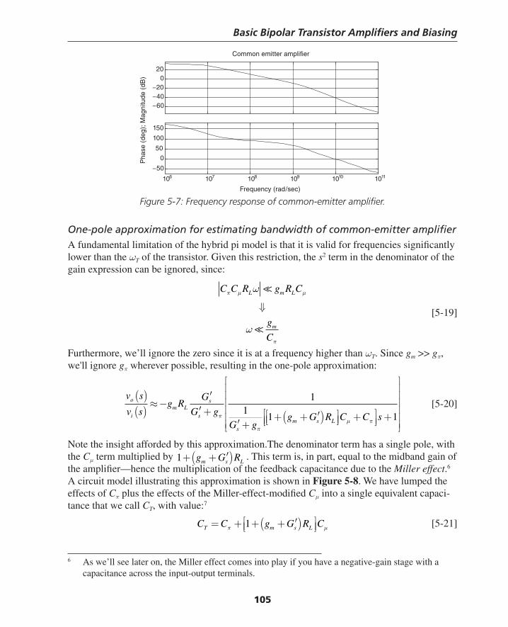
Basic Bipolar Transistor Amplifi ers and Biasing
105
Figure 5-7: Frequency response of common-emitter amplifi er.
One-pole approximation for estimating bandwidth of common-emitter amplifi erA fundamental limitation of the hybrid pi model is that it is valid for frequencies signifi cantly lower than the ωT of the transistor. Given this restriction, the s2 term in the denominator of the gain expression can be ignored, since:
C C R g R C
g
C
L m L
m
π μ μ
π
ω
ω
⇓ [5-19]
Furthermore, we’ll ignore the zero since it is at a frequency higher than ωT. Since gm >> gπ, we'll ignore gπ wherever possible, resulting in the one-pole approximation:
v s
v sg R
G
G gG g
g G R C C
o
im L
s
s
sm s L
( )( )
≈ −′
′ +′ +
+ + ′( )⎡⎣⎢
⎤⎦⎥ +⎡
⎣π
πμ π
11
1⎢⎢⎤⎦⎥ +
⎡
⎣
⎢⎢⎢⎢⎢⎢
⎤
⎦
⎥⎥⎥⎥⎥⎥
s 1 [5-20]
Note the insight afforded by this approximation.The denominator term has a single pole, with the Cμ term multiplied by 1+ + ′( )g G Rm s L
. This term is, in part, equal to the midband gain of the amplifi er—hence the multiplication of the feedback capacitance due to the Miller effect.6 A circuit model illustrating this approximation is shown in Figure 5-8. We have lumped the effects of Cπ plus the effects of the Miller-effect-modifi ed Cμ into a single equivalent capaci-tance that we call CT, with value:7
C C g G R CT m s L= + + + ′( )⎡⎣⎢
⎤⎦⎥π μ1 [5-21]
6 As we’ll see later on, the Miller effect comes into play if you have a negative-gain stage with a capacitance across the input-output terminals.
Frequency (rad/sec)
Pha
se (
deg)
; Mag
nitu
de (
dB)
Common emitter amplifier
−60−40−20
020
106 107 108 109 1010 1011
−50
0
50
100
150
Thompson Book.indb 105 3/20/2006 11:34:26 AM
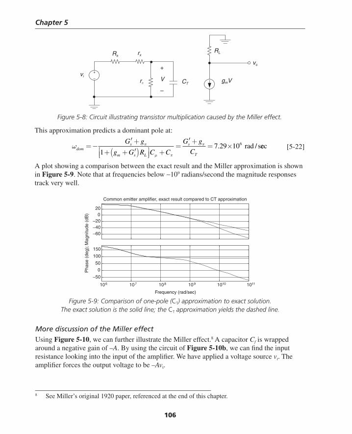
Chapter 5
106
Figure 5-8: Circuit illustrating transistor multiplication caused by the Miller effect.
This approximation predicts a dominant pole at:
ω π
μ π
πdom
s
m s L
s
T
G g
g G R C C
G g
C= −
′ +
+ + ′( )⎡⎣⎢
⎤⎦⎥ +
=′ +
= ×1
7 29 106. / srad eec [5-22]
A plot showing a comparison between the exact result and the Miller approximation is shown in Figure 5-9. Note that at frequencies below ∼109 radians/second the magnitude responses track very well.
8 See Miller’s original 1920 paper, referenced at the end of this chapter.
Rs rx
rπ
vi
CT
+
V
–
RL
gmV
vo
Figure 5-9: Comparison of one-pole (CT) approximation to exact solution. The exact solution is the solid line; the CT approximation yields the dashed line.
More discussion of the Miller effectUsing Figure 5-10, we can further illustrate the Miller effect.8 A capacitor Cf is wrapped around a negative gain of –A. By using the circuit of Figure 5-10b, we can fi nd the input resistance looking into the input of the amplifi er. We have applied a voltage source vt. The amplifi er forces the output voltage to be –Avt.
Frequency (rad/sec)
Pha
se (
deg)
; Mag
nitu
de (
dB)
Common emitter amplifier, exact result compared to CT approximation
−60−40−20
020
106 107 108 109 1010 1011
−50
0
50
100
150
Thompson Book.indb 106 3/20/2006 11:34:27 AM
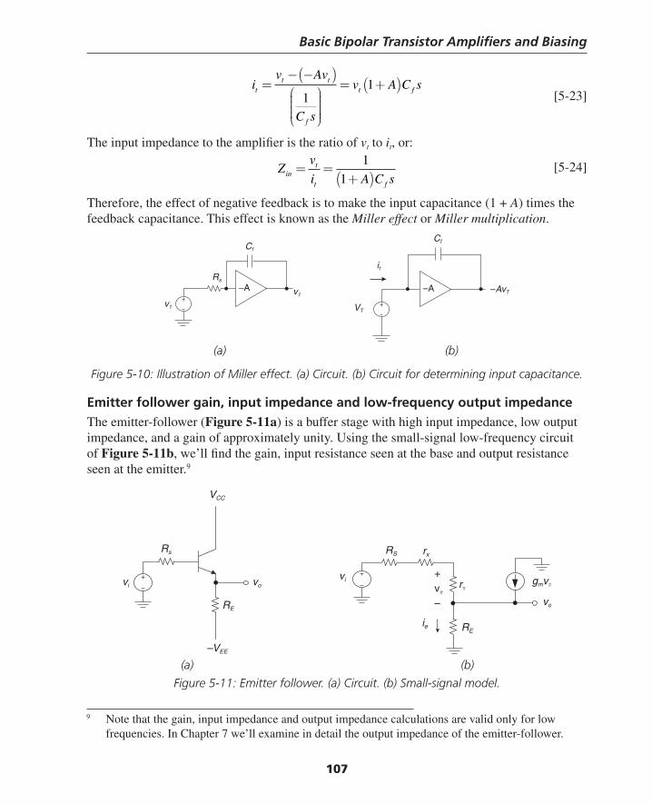
Basic Bipolar Transistor Amplifi ers and Biasing
107
i
v Av
C s
v A C stt t
f
t f=− −( )⎛
⎝⎜⎜⎜⎜
⎞
⎠
⎟⎟⎟⎟⎟
= +( )1
1 [5-23]
The input impedance to the amplifi er is the ratio of vt to it, or:
Zv
i A C sint
t f
= =+( )
1
1 [5-24]
Therefore, the effect of negative feedback is to make the input capacitance (1 + A) times the feedback capacitance. This effect is known as the Miller effect or Miller multiplication.
Cf
VT
Cf
–A –A
it
–AvTv1
v1
Rs
9 Note that the gain, input impedance and output impedance calculations are valid only for low frequencies. In Chapter 7 we’ll examine in detail the output impedance of the emitter-follower.
(a) (b)
Figure 5-10: Illustration of Miller effect. (a) Circuit. (b) Circuit for determining input capacitance.
Emitter follower gain, input impedance and low-frequency output impedanceThe emitter-follower (Figure 5-11a) is a buffer stage with high input impedance, low output impedance, and a gain of approximately unity. Using the small-signal low-frequency circuit of Figure 5-11b, we’ll fi nd the gain, input resistance seen at the base and output resistance seen at the emitter.9
Rs
+vπ
–
ie RE
rπ
RS rx
vivi vo gmvπ
vo
–VEE
VCC
RE
(a) (b)
Figure 5-11: Emitter follower. (a) Circuit. (b) Small-signal model.
Thompson Book.indb 107 3/20/2006 11:34:27 AM
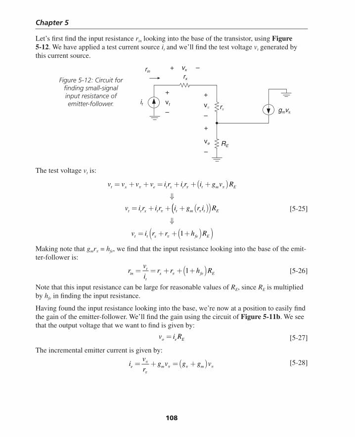
Chapter 5
108
Let’s fi rst fi nd the input resistance rin looking into the base of the transistor, using Figure 5-12. We have applied a test current source it and we’ll fi nd the test voltage vt generated by this current source.
The test voltage vt is:
v v v v i r i r i g v R
v i r i r i g r i
t x e t x t t m E
t t x t t m t
= + + = + + +( )⇓
= + + + ( )
π π π
π π(( )⇓
= + + +( )( )
R
v i r r h R
E
t t x fe Eπ 1
[5-25]
Making note that gmrπ = hfe, we fi nd that the input resistance looking into the base of the emit-ter-follower is:
rv
ir r h Rin
t
tx fe E= = + + +( )π 1 [5-26]
Note that this input resistance can be large for reasonable values of RE, since RE is multiplied by hfe in fi nding the input resistance.
Having found the input resistance looking into the base, we’re now at a position to easily fi nd the gain of the emitter-follower. We’ll fi nd the gain using the circuit of Figure 5-11b. We see that the output voltage that we want to fi nd is given by:
v i Ro e E= [5-27]
The incremental emitter current is given by:
iv
rg v g g ve m m= + = +( )π
ππ π π
[5-28]
rin
+
vπ
–
RE
rπ
itgmvπ
+
ve
–
+
vt
–
+ vx –rxFigure 5-12: Circuit for
fi nding small-signal input resistance of emitter-follower.
Thompson Book.indb 108 3/20/2006 11:34:28 AM
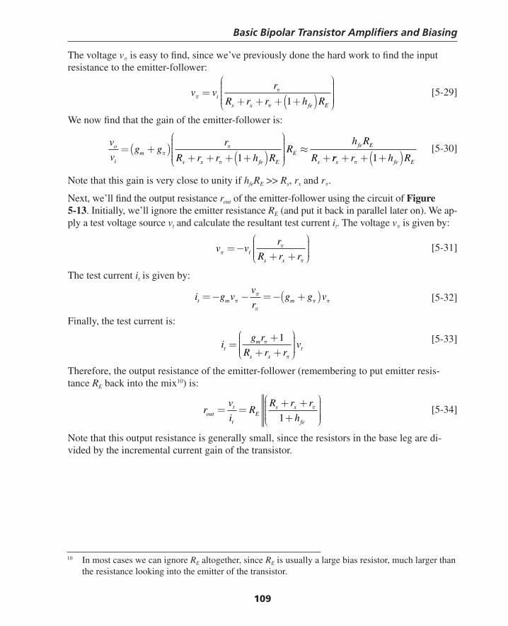
Basic Bipolar Transistor Amplifi ers and Biasing
109
The voltage vπ is easy to fi nd, since we’ve previously done the hard work to fi nd the input resistance to the emitter-follower:
v vr
R r r h Ri
s x fe E
ππ
π
=+ + + +( )
⎛
⎝
⎜⎜⎜⎜⎜
⎞
⎠
⎟⎟⎟⎟⎟⎟1 [5-29]
We now fi nd that the gain of the emitter-follower is:
v
vg g
r
R r r h RR
h R
Ro
im
s x fe E
Efe E
s
= +( )+ + + +( )
⎛
⎝
⎜⎜⎜⎜⎜
⎞
⎠
⎟⎟⎟⎟⎟⎟≈
+ππ
π 1 rr r h Rx fe E+ + +( )π 1 [5-30]
Note that this gain is very close to unity if hfeRE >> Rs, rx and rπ.
Next, we’ll fi nd the output resistance rout of the emitter-follower using the circuit of Figure 5-13. Initially, we’ll ignore the emitter resistance RE (and put it back in parallel later on). We ap-ply a test voltage source vt and calculate the resultant test current it. The voltage vπ is given by:
v vr
R r rts x
ππ
π
= −+ +
⎛
⎝⎜⎜⎜⎜
⎞
⎠⎟⎟⎟⎟ [5-31]
The test current it is given by:
i g vv
rg g vt m m= − − = − +( )π
π
ππ π [5-32]
Finally, the test current is:
ig r
R r rvt
m
s xt=
++ +
⎛
⎝⎜⎜⎜⎜
⎞
⎠⎟⎟⎟⎟
π
π
1 [5-33]
Therefore, the output resistance of the emitter-follower (remembering to put emitter resis-tance RE back into the mix10) is:
rv
iR
R r r
houtt
tE
s x
fe
= =+ ++
⎛
⎝⎜⎜⎜⎜
⎞
⎠
⎟⎟⎟⎟⎟π
1 [5-34]
Note that this output resistance is generally small, since the resistors in the base leg are di-vided by the incremental current gain of the transistor.
10 In most cases we can ignore RE altogether, since RE is usually a large bias resistor, much larger than the resistance looking into the emitter of the transistor.
Thompson Book.indb 109 3/20/2006 11:34:29 AM
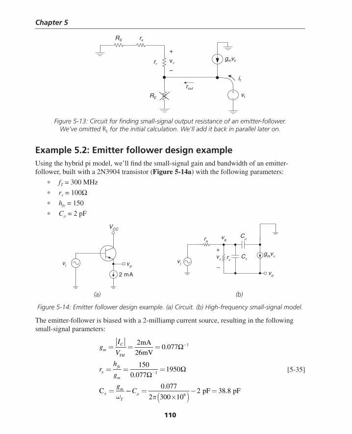
Chapter 5
110
Figure 5-13: Circuit for fi nding small-signal output resistance of an emitter-follower. We’ve omitted RE for the initial calculation. We’ll add it back in parallel later on.
Example 5.2: Emitter follower design exampleUsing the hybrid pi model, we’ll fi nd the small-signal gain and bandwidth of an emitter- follower, built with a 2N3904 transistor (Figure 5-14a) with the following parameters:
• fT = 300 MHz
• rx = 100Ω• hfe = 150
• Cμ = 2 pF
+
vπ
–
RE
rπgmvπ
rxRS
rout
it
vt
VCC
2 mA
vi vo
+
–
rx
rπCπ
Cμ
gmvπvπ
vo
va
vi
(a) (b)
Figure 5-14: Emitter follower design example. (a) Circuit. (b) High-frequency small-signal model.
The emitter-follower is biased with a 2-milliamp current source, resulting in the following small-signal parameters:
gI
V
rh
g
g
mC
TH
fe
m
m
T
= = =
= = =
=
−
−
2
260 077
150
0 0771950
1
1
mA
mV.
.
Ω
ΩΩπ
π ωC −− =
×( )− =Cμ π
0 077
2 300 102 38 8
6
..pF pF
[5-35]
Thompson Book.indb 110 3/20/2006 11:34:29 AM
Basic Bipolar Transistor Amplifi ers and Biasing
111
The small-signal model for the emitter-follower is shown in Figure 5-14b. Using this small-signal model, the node equations at the va and vo nodes are:
1 0
2 0
) −( ) + −( ) +( )− =
) −( ) + +( )=
v v g v v g C s v C s
v v g C s g
i a x o a a
a o m
π π μ
π π
[5-36]
Putting this into matrix form, and making the approximation that gm = hfegπ >> gπ results in:
[5-37]
1
2
) − + + +( )⎡⎣⎢
⎤⎦⎥ + +( )= −
) +( )−
v g g C C s v g C s v g
v g C s v g
a x o i x
a m o
π π μ π π
π mm C s+( )=π 0
or:
− + + +( )⎡⎣⎢
⎤⎦⎥ +
+ − +( )
⎡
⎣
⎢⎢⎢
⎤
⎦
⎥⎥⎥
⎧⎨
g g C C s g C s
g C s g C s
v
vx
m m
a
o
π π μ π π
π π
⎪⎪⎪⎩⎪⎪
⎫⎬⎪⎪⎭⎪⎪
=−⎧
⎨⎪⎪⎩⎪⎪
⎫⎬⎪⎪⎭⎪⎪
v gi x
0
Using Cramer’s rule (see Chapter 16) to solve for the transfer function vo/vi results in:
v
g g C C s v g
g C s
g go
x i x
m
x
=
− + + +( )⎡⎣⎢
⎤⎦⎥ −
+
⎡
⎣
⎢⎢⎢
⎤
⎦
⎥⎥⎥
− +
det
det
π π μ
π
π
0
++ +( )⎡⎣⎢
⎤⎦⎥ +
+ − +( )
⎡
⎣
⎢⎢⎢
⎤
⎦
⎥⎥⎥
C C s g C s
g C s g C sm m
π μ π π
π π
[5-38]
Solving for vo/vi:
v s
v s
C
gs
r C C
gs r C
C
gs
o
i
m
x
mx
m
( )( )
≈+
+ +⎡
⎣⎢⎢
⎤
⎦⎥⎥ +
π
π μμ
π
1
12 [5-39]
Note that the denominator is exactly in the form:
τ τ τ τ τ τ1 2 1 22
1 21 1 1s s s s+( ) +( )= + +( ) + [5-40]
Therefore, the two poles are at frequencies:
ωτ
ωτ
π
μ
pm
px
g
C
r C
11
9
22
9
11 95 10
1 15 10
= − = − = − ×
= − = − = − ×
. / sec
/ s
rad
rad eec [5-41]
Thompson Book.indb 111 3/20/2006 11:34:29 AM

Chapter 5
112
Note that there is also a zero at Cπ/gm, which in this simplifi ed model exactly cancels the pole at –ωp1. Therefore, the bandwidth for this circuit is:
ω ω
ωπ
h p
hh
≈ − = ×
≈ =
295 10
2795
rad
MHz
/ sec
f [5-42]
which matches closely the SPICE result. Actually, the pole and zero don’t exactly cancel. This is an artifact of our ignoring gπ as compared to gm. Also, the preceding result must be taken with a grain of salt, as the model predicts a bandwidth in excess of the fT of the transistor.
A SPICE result showing the gain and bandwidth is shown in Figure 5-15. This result shows that the gain = 1 (as expected) and the –3dB bandwidth is approximately 800 MHz.
11 Said another way, the differential amplifi er is designed to have high “differential-mode” gain and very low “common-mode” gain.
Figure 5-15: SPICE result for emitter-follower, showing bandwidth of approximately 800 MHz.
Differential amplifi erThe transistor differential amplifi er (Figure 5-16) is a ubiquitous building block used com-monly as the front-end of an operational amplifi er. The differential amplifi er is used to amplify the difference between its two inputs, while rejecting the DC value common to the two inputs.11
If we do KVL around the voltage source and base-emitter junctions, we fi nd:
− + − + =V V V VBE BE1 1 2 2 0 [5-43]
Thompson Book.indb 112 3/20/2006 11:34:30 AM
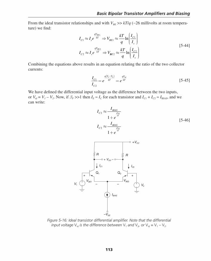
Basic Bipolar Transistor Amplifi ers and Biasing
113
From the ideal transistor relationships and with VBE >> kT/q (∼26 millivolts at room tempera-ture) we fi nd:
I I e VkT
q
I
I
I I e V
C s
qV
kTBE
C
s
C s
qV
kT
BE
BE
1 11
2
1
2
≈ ⇒ ≈⎛
⎝⎜⎜⎜⎜
⎞
⎠⎟⎟⎟⎟
≈ ⇒
ln
BBEC
s
kT
q
I
I22≈
⎛
⎝⎜⎜⎜⎜
⎞
⎠⎟⎟⎟⎟
ln
[5-44]
Combining the equations above results in an equation relating the ratio of the two collector currents:
I
Ie eC
C
q V V
kT
qV
kTid
1
2
1 2
= =−( )
[5-45]
We have defi ned the differential input voltage as the difference between the two inputs, or Vid = V1 – V2. Now, if βF >>1 then IE ≈ IC for each transistor and IC1 + IC2 ≈ IBIAS, and we can write:
II
e
II
e
CBIAS
CBIAS
qVidkT
qVidkT
2
2
1
1
≈+
≈+
[5-46]
Figure 5-16: Ideal transistor differential amplifi er. Note that the differential input voltage Vid is the difference between V1 and V2, or Vid = V1 – V2.
V1
VBE1
IBIAS
–VEE
V2
VBE2
– –
+ +
+ VOD –
R R
IC2IC1
Q1 Q2
+VCC
Thompson Book.indb 113 3/20/2006 11:34:30 AM
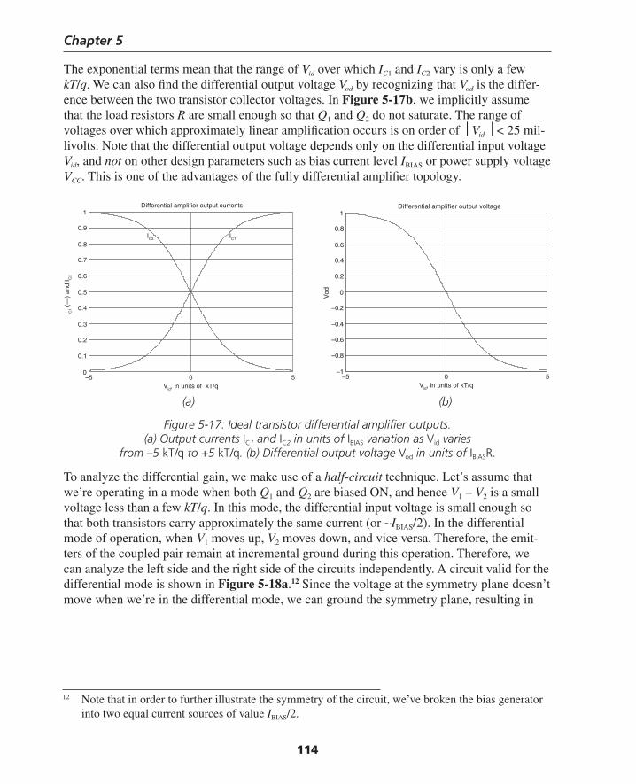
Chapter 5
114
The exponential terms mean that the range of Vid over which IC1 and IC2 vary is only a few kT/q. We can also fi nd the differential output voltage Vod by recognizing that Vod is the differ-ence between the two transistor collector voltages. In Figure 5-17b, we implicitly assume that the load resistors R are small enough so that Q1 and Q2 do not saturate. The range of voltages over which approximately linear amplifi cation occurs is on order of ⎮Vid ⎮< 25 mil-livolts. Note that the differential output voltage depends only on the differential input voltage Vid, and not on other design parameters such as bias current level IBIAS or power supply voltage VCC. This is one of the advantages of the fully differential amplifi er topology.
–5 0 50
0.1
0.2
0.3
0.4
0.5
0.6
0.7
0.8
0.9
1Differential amplifier output currents
Vid, in units of kT/q
IC1IC2
I C1
(—)
and
I C2
(a) (b)
Figure 5-17: Ideal transistor differential amplifi er outputs. (a) Output currents IC1 and IC2 in units of IBIAS variation as Vid varies
from –5 kT/q to +5 kT/q. (b) Differential output voltage Vod in units of IBIASR.
To analyze the differential gain, we make use of a half-circuit technique. Let’s assume that we’re operating in a mode when both Q1 and Q2 are biased ON, and hence V1 – V2 is a small voltage less than a few kT/q. In this mode, the differential input voltage is small enough so that both transistors carry approximately the same current (or ∼IBIAS/2). In the differential mode of operation, when V1 moves up, V2 moves down, and vice versa. Therefore, the emit-ters of the coupled pair remain at incremental ground during this operation. Therefore, we can analyze the left side and the right side of the circuits independently. A circuit valid for the differential mode is shown in Figure 5-18a.12 Since the voltage at the symmetry plane doesn’t move when we’re in the differential mode, we can ground the symmetry plane, resulting in
–5 0 5–1
–0.8
–0.6
–0.4
–0.2
0
0.2
0.4
0.6
0.8
1Differential amplifier output voltage
Vid, in units of kT/q
Vod
12 Note that in order to further illustrate the symmetry of the circuit, we’ve broken the bias generator into two equal current sources of value IBIAS/2.
Thompson Book.indb 114 3/20/2006 11:34:31 AM
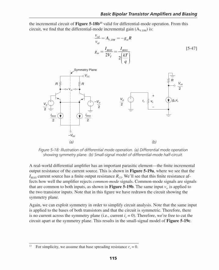
Basic Bipolar Transistor Amplifi ers and Biasing
115
the incremental circuit of Figure 5-18b13 valid for differential-mode operation. From this circuit, we fi nd that the differential-mode incremental gain (AV, DM) is:
v
vA g R
gI
V
I
kT
q
od
idV DM m
mBIAS
T
BIAS
= = −
= =⎛
⎝⎜⎜⎜
⎞
⎠⎟⎟⎟⎟
,
22
[5-47]
13 For simplicity, we assume that base spreading resistance rx = 0.
–VEE
R R
VCC
Symmetry Plane
–Vid
2Vid
2
IBIAS
2
IBIAS
2
Vid
2
Vod
2
rπ vπgmvπ
R
+
–
+ Vod –
(a) (b)
Figure 5-18: Illustration of differential mode operation. (a) Differential mode operation showing symmetry plane. (b) Small-signal model of differential-mode half-circuit.
A real-world differential amplifi er has an important parasitic element—the fi nite incremental output resistance of the current source. This is shown in Figure 5-19a, where we see that the IBIAS current source has a fi nite output resistance RCS. We’ll see that this fi nite resistance af-fects how well the amplifi er rejects common-mode signals. Common-mode signals are signals that are common to both inputs, as shown in Figure 5-19b. The same input vic is applied to the two transistor inputs. Note that in this fi gure we have redrawn the circuit showing the symmetry plane.
Again, we can exploit symmetry in order to simplify circuit analysis. Note that the same input is applied to the bases of both transistors and that the circuit is symmetric. Therefore, there is no current across the symmetry plane (i.e., current ix = 0). Therefore, we’re free to cut the circuit apart at the symmetry plane. This results in the small-signal model of Figure 5-19c.
Thompson Book.indb 115 3/20/2006 11:34:31 AM
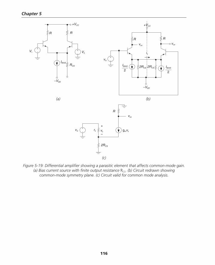
Chapter 5
116
–VEE
R
+VCC
R
V1 V2
IBIASRCS
R
rπ vπ
+
–
2RCS
vic
voc
gmvπ
voc
vic
IBIAS
22RCS 2RCS IBIAS
2
–VEE
R
voc
R
+VCC
ix
(a) (b)
(c)
Figure 5-19: Differential amplifi er showing a parasitic element that affects common-mode gain. (a) Bias current source with fi nite output resistance RCS. (b) Circuit redrawn showing
common-mode symmetry plane. (c) Circuit valid for common mode analysis.
Thompson Book.indb 116 3/20/2006 11:34:32 AM
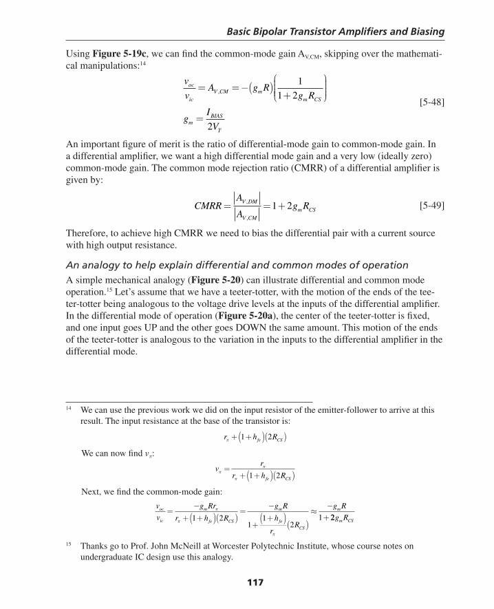
Basic Bipolar Transistor Amplifi ers and Biasing
117
Using Figure 5-19c, we can fi nd the common-mode gain AV,CM, skipping over the mathemati-cal manipulations:14
v
vA g R
g R
gI
V
oc
icV CM m
m CS
mBIAS
T
= = −( )+
⎛
⎝⎜⎜⎜⎜
⎞
⎠⎟⎟⎟⎟
=
,
1
1 2
2
[5-48]
An important fi gure of merit is the ratio of differential-mode gain to common-mode gain. In a differential amplifi er, we want a high differential mode gain and a very low (ideally zero) common-mode gain. The common mode rejection ratio (CMRR) of a differential amplifi er is given by:
CMRRA
Ag RV DM
V CM
m CS= = +,
,
1 2 [5-49]
Therefore, to achieve high CMRR we need to bias the differential pair with a current source with high output resistance.
An analogy to help explain differential and common modes of operationA simple mechanical analogy (Figure 5-20) can illustrate differential and common mode operation.15 Let’s assume that we have a teeter-totter, with the motion of the ends of the tee-ter-totter being analogous to the voltage drive levels at the inputs of the differential amplifi er. In the differential mode of operation (Figure 5-20a), the center of the teeter-totter is fi xed, and one input goes UP and the other goes DOWN the same amount. This motion of the ends of the teeter-totter is analogous to the variation in the inputs to the differential amplifi er in the differential mode.
14 We can use the previous work we did on the input resistor of the emitter-follower to arrive at this result. The input resistance at the base of the transistor is:
r h Rfe CSπ + +( )( )1 2
We can now fi nd vπ:
vr
r h Rfe CS
ππ
π
=+ +( )( )1 2
Next, we fi nd the common-mode gain:
v
v
g Rr
r h R
g R
h
rR
g Roc
ic
m
fe CS
m
fe
CS
m=−
+ +( )( )=
−
++( )
( )≈
−+
π
π
π
1 21
12
1 22g Rm CS
15 Thanks go to Prof. John McNeill at Worcester Polytechnic Institute, whose course notes on undergraduate IC design use this analogy.
Thompson Book.indb 117 3/20/2006 11:34:32 AM
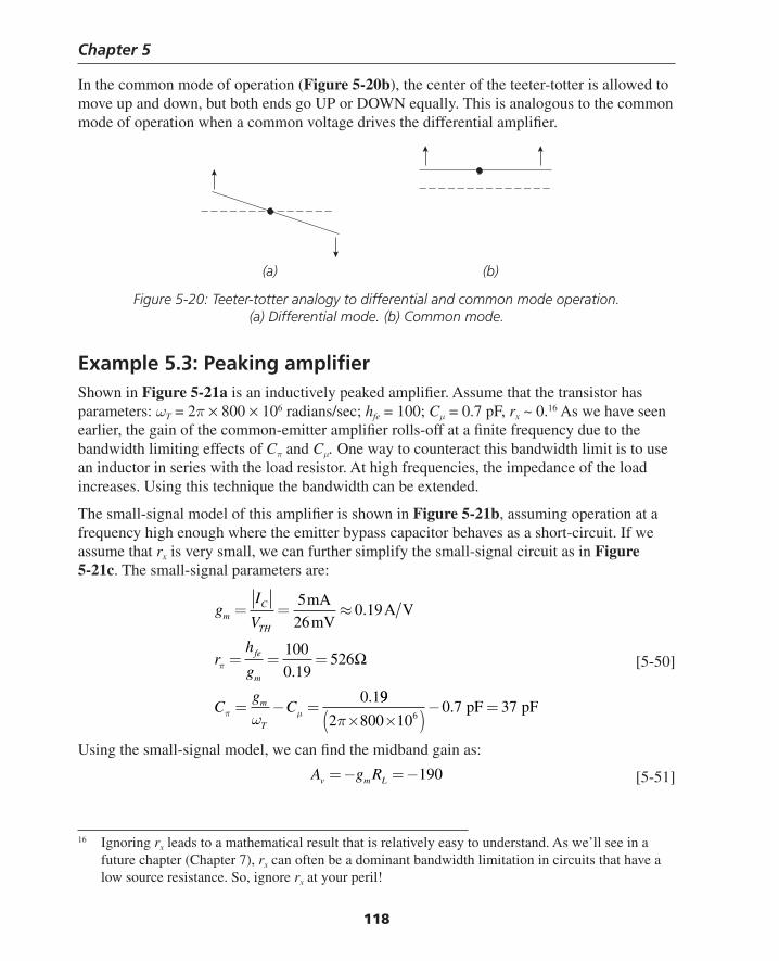
Chapter 5
118
In the common mode of operation (Figure 5-20b), the center of the teeter-totter is allowed to move up and down, but both ends go UP or DOWN equally. This is analogous to the common mode of operation when a common voltage drives the differential amplifi er.
16 Ignoring rx leads to a mathematical result that is relatively easy to understand. As we’ll see in a future chapter (Chapter 7), rx can often be a dominant bandwidth limitation in circuits that have a low source resistance. So, ignore rx at your peril!
(a) (b)
Figure 5-20: Teeter-totter analogy to differential and common mode operation. (a) Differential mode. (b) Common mode.
Example 5.3: Peaking amplifi erShown in Figure 5-21a is an inductively peaked amplifi er. Assume that the transistor has parameters: ωT = 2π × 800 × 106 radians/sec; hfe = 100; Cμ = 0.7 pF, rx ~ 0.16 As we have seen earlier, the gain of the common-emitter amplifi er rolls-off at a fi nite frequency due to the bandwidth limiting effects of Cπ and Cμ. One way to counteract this bandwidth limit is to use an inductor in series with the load resistor. At high frequencies, the impedance of the load increases. Using this technique the bandwidth can be extended.
The small-signal model of this amplifi er is shown in Figure 5-21b, assuming operation at a frequency high enough where the emitter bypass capacitor behaves as a short-circuit. If we assume that rx is very small, we can further simplify the small-signal circuit as in Figure 5-21c. The small-signal parameters are:
gI
V
rh
g
Cg
C
mC
TH
fe
m
m
T
= = ≈
= = =
= − =
5
260 19
100
0 19526
0 1
mA
mVA V.
.
.
π
π μω
Ω
99
2 800 100 7 37
6π× ×( )− =. pF pF
[5-50]
Using the small-signal model, we can fi nd the midband gain as:
A g Rv m L= − = −190 [5-51]
Thompson Book.indb 118 3/20/2006 11:34:32 AM
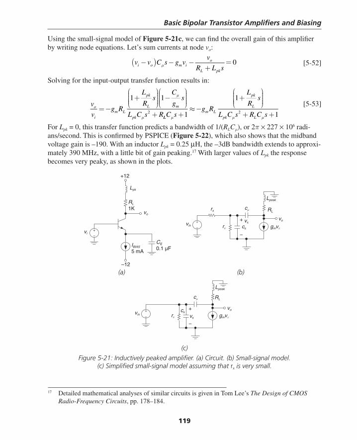
Basic Bipolar Transistor Amplifi ers and Biasing
119
Using the small-signal model of Figure 5-21c, we can fi nd the overall gain of this amplifi er by writing node equations. Let’s sum currents at node vo:
v v C s g vv
R L si o m io
L pk
−( ) − −+
=μ 0 [5-52]
Solving for the input-output transfer function results in:
v
vg R
L
Rs
C
gs
L C s Ro
im L
pk
L m
pk
= −
+⎛
⎝⎜⎜⎜⎜
⎞
⎠⎟⎟⎟⎟
−⎛
⎝⎜⎜⎜⎜
⎞
⎠⎟⎟⎟⎟
+
1 1
2
μ
μ LLm L
pk
L
pk LC sg R
L
Rs
L C s R C sμ μ μ+≈ −
+⎛
⎝⎜⎜⎜⎜
⎞
⎠⎟⎟⎟⎟
+ +1
1
12
[5-53]
For Lpk = 0, this transfer function predicts a bandwidth of 1/(RLCμ), or 2π × 227 × 106 radi-ans/second. This is confi rmed by PSPICE (Figure 5-22), which also shows that the midband voltage gain is –190. With an inductor Lpk = 0.25 μH, the –3dB bandwidth extends to approxi-mately 390 MHz, with a little bit of gain peaking.17 With larger values of Lpk the response becomes very peaky, as shown in the plots.
(a) (b)
17 Detailed mathematical analyses of similar circuits is given in Tom Lee’s The Design of CMOS Radio-Frequency Circuits, pp. 178–184.
+12
vo
Lpk
RL
1K
vi
IBIAS
5 mA
CE
0.1 µF
–12
vin rπ cπ
cμrx RL
Lpeak
vπ+
−
gmvπ
vin rπ
cπ
cμ RL
Lpeak
vπ
+
−
gmvπ
vo
vo
(c)
Figure 5-21: Inductively peaked amplifi er. (a) Circuit. (b) Small-signal model. (c) Simplifi ed small-signal model assuming that rx is very small.
Thompson Book.indb 119 3/20/2006 11:34:33 AM
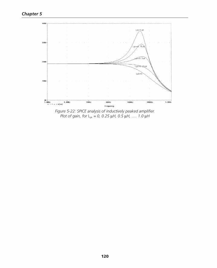
Chapter 5
120
Figure 5-22: SPICE analysis of inductively peaked amplifi er. Plot of gain, for Lpk = 0, 0.25 μH, 0.5 μH, …. 1.0 μH
Thompson Book.indb 120 3/20/2006 11:34:33 AM
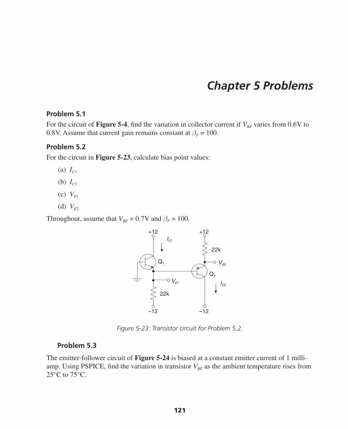
121
Chapter 5 Problems
Problem 5.1For the circuit of Figure 5-4, fi nd the variation in collector current if VBE varies from 0.6V to 0.8V. Assume that current gain remains constant at βF = 100.
Problem 5.2For the circuit in Figure 5-23, calculate bias point values:
(a) IC1
(b) IC2
(c) VE1
(d) VE2
Throughout, assume that VBE = 0.7V and βF = 100.
VE1
VE2
IC1
IC2
+12 +12
–12–12
Q2
Q1
22k
22k
Figure 5-23: Transistor circuit for Problem 5.2.
Problem 5.3
The emitter-follower circuit of Figure 5-24 is biased at a constant emitter current of 1 milli-amp. Using PSPICE, fi nd the variation in transistor VBE as the ambient temperature rises from 25°C to 75°C.
Thompson Book.indb 121 3/20/2006 11:34:34 AM
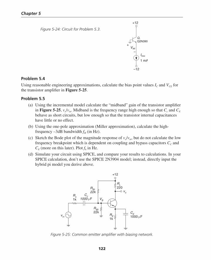
Chapter 5
122
Problem 5.4Using reasonable engineering approximations, calculate the bias point values IC and VCE for the transistor amplifi er in Figure 5-25.
Problem 5.5(a) Using the incremental model calculate the “midband” gain of the transistor amplifi er
in Figure 5-25, vo/vin. Midband is the frequency range high enough so that Cc and CE behave as short circuits, but low enough so that the transistor internal capacitances have little or no effect.
(b) Using the one-pole approximation (Miller approximation), calculate the high- frequency –3dB bandwidth fH (in Hz).
(c) Sketch the Bode plot of the magnitude response of vo/vin, but do not calculate the low frequency breakpoint which is dependent on coupling and bypass capacitors CC and CE (more on this later). Plot fh in Hz.
(d) Simulate your circuit using SPICE, and compare your results to calculations. In your SPICE calculation, don’t use the SPICE 2N3904 model; instead, directly input the hybrid pi model you derive above.
Figure 5-25: Common emitter amplifi er with biasing network.
VBE
Ibias
–12
1 mA
+12
Q1
Q2N390
–
+
vin
Rs1k
vo
+12
Cc1000 μF
CE1000 μFRE
1k
RB222k
RB122k
RL220
VB
Figure 5-24: Circuit for Problem 5.3.
Thompson Book.indb 122 3/20/2006 11:34:34 AM
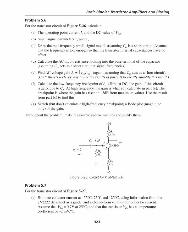
Basic Bipolar Transistor Amplifi ers and Biasing
123
Problem 5.6For the transistor circuit of Figure 5-26, calculate:
(a) The operating point current Ic and the DC value of Vout.
(b) Small signal parameters rπ and gm.
(c) Draw the mid-frequency small-signal model, assuming Cin is a short circuit. Assume that the frequency is low enough so that the transistor internal capacitances have no effect.
(d) Calculate the AC input resistance looking into the base terminal of the capacitor (assuming Cin acts as a short circuit at signal frequencies).
(e) Find AC voltage gain Av = ⏐vout/vin⏐ (again, assuming that Cin acts as a short circuit). (Hint: there’s a clever way to use the results of part (d) to greatly simplify this result.)
(f) Calculate the low-frequency breakpoint of Av. (Hint: at DC, the gain of this circuit is zero, due to Cin. At high frequency, the gain is what you calculate in part (e). The breakpoint is where the gain has risen to –3dB from maximum value). Use the result from part (c) to fi nd this.
(g) Sketch (but don’t calculate a high-frequency breakpoint) a Bode plot (magnitude only) of the gain.
Throughout the problem, make reasonable approximations and justify them.
2N3904
RL4.7k
+36
RE1k
–5
vout
RB1k
Cin 1 uF
vin
Figure 5-26: Circuit for Problem 5.6.
Problem 5.7For the transistor circuit of Figure 5-27,
(a) Estimate collector current at –55°C, 25°C and 125°C, using information from the 2N2222 datasheet as a guide, and a closed-form solution for collector current. Assume that VBE = 0.7V at 25°C, and that the transistor VBE has a temperature coeffi cient of –2 mV/ºC.
Thompson Book.indb 123 3/20/2006 11:34:35 AM
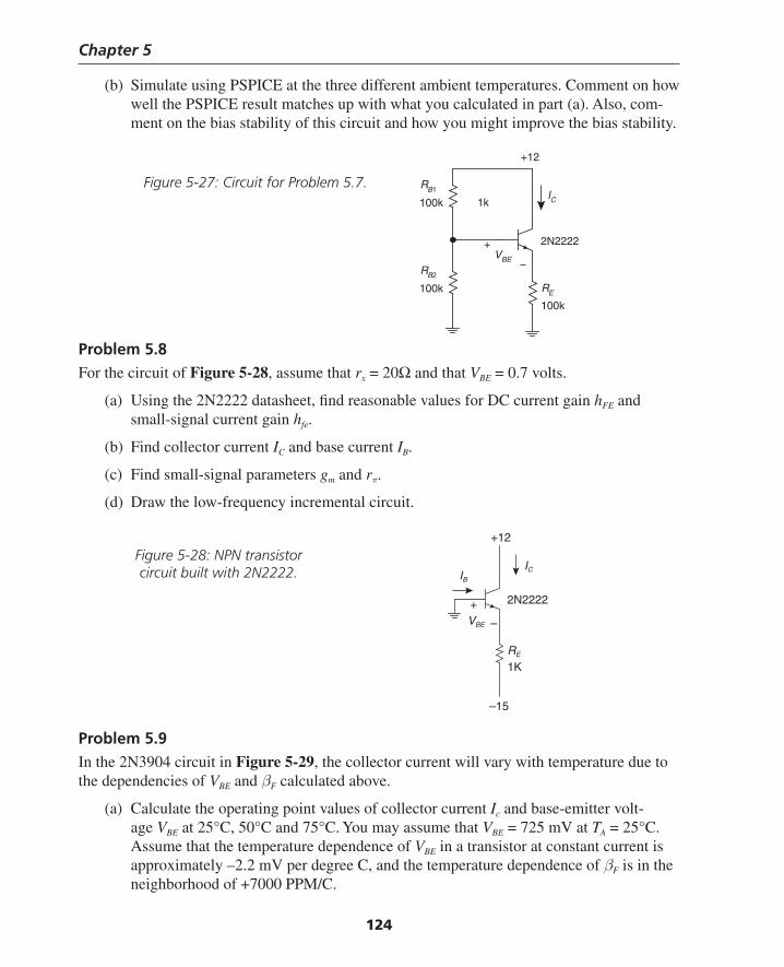
Chapter 5
124
(b) Simulate using PSPICE at the three different ambient temperatures. Comment on how well the PSPICE result matches up with what you calculated in part (a). Also, com-ment on the bias stability of this circuit and how you might improve the bias stability.
Problem 5.8For the circuit of Figure 5-28, assume that rx = 20Ω and that VBE = 0.7 volts.
(a) Using the 2N2222 datasheet, fi nd reasonable values for DC current gain hFE and small-signal current gain hfe.
(b) Find collector current IC and base current IB.
(c) Find small-signal parameters gm and rπ.
(d) Draw the low-frequency incremental circuit.
2N2222
100k
RB1
100k
RB2
1k
RE
100k
+12
VBE
+
IC
−
2N2222
IC
+12
IB
VBE
RE
1K
–15
+
–
Problem 5.9In the 2N3904 circuit in Figure 5-29, the collector current will vary with temperature due to the dependencies of VBE and βF calculated above.
(a) Calculate the operating point values of collector current Ic and base-emitter volt-age VBE at 25°C, 50°C and 75°C. You may assume that VBE = 725 mV at TA = 25°C. Assume that the temperature dependence of VBE in a transistor at constant current is approximately –2.2 mV per degree C, and the temperature dependence of βF is in the neighborhood of +7000 PPM/C.
Figure 5-27: Circuit for Problem 5.7.
Figure 5-28: NPN transistor circuit built with 2N2222.
Thompson Book.indb 124 3/20/2006 11:34:35 AM
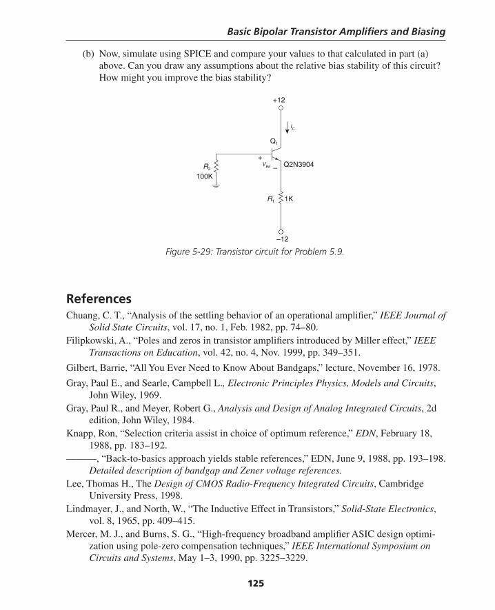
Basic Bipolar Transistor Amplifi ers and Biasing
125
(b) Now, simulate using SPICE and compare your values to that calculated in part (a) above. Can you draw any assumptions about the relative bias stability of this circuit? How might you improve the bias stability?
Figure 5-29: Transistor circuit for Problem 5.9.
Q2N3904
R1 1K
R2
100K
Q1
+12
–12
VBE
IC
+
–
ReferencesChuang, C. T., “Analysis of the settling behavior of an operational amplifi er,” IEEE Journal of
Solid State Circuits, vol. 17, no. 1, Feb. 1982, pp. 74–80.Filipkowski, A., “Poles and zeros in transistor amplifi ers introduced by Miller effect,” IEEE
Transactions on Education, vol. 42, no. 4, Nov. 1999, pp. 349–351.
Gilbert, Barrie, “All You Ever Need to Know About Bandgaps,” lecture, November 16, 1978.
Gray, Paul E., and Searle, Campbell L., Electronic Principles Physics, Models and Circuits, John Wiley, 1969.
Gray, Paul R., and Meyer, Robert G., Analysis and Design of Analog Integrated Circuits, 2d edition, John Wiley, 1984.
Knapp, Ron, “Selection criteria assist in choice of optimum reference,” EDN, February 18, 1988, pp. 183–192.
———, “Back-to-basics approach yields stable references,” EDN, June 9, 1988, pp. 193–198. Detailed description of bandgap and Zener voltage references.
Lee, Thomas H., The Design of CMOS Radio-Frequency Integrated Circuits, Cambridge University Press, 1998.
Lindmayer, J., and North, W., “The Inductive Effect in Transistors,” Solid-State Electronics, vol. 8, 1965, pp. 409–415.
Mercer, M. J., and Burns, S. G., “High-frequency broadband amplifi er ASIC design optimi-zation using pole-zero compensation techniques,” IEEE International Symposium on Circuits and Systems, May 1–3, 1990, pp. 3225–3229.
Thompson Book.indb 125 3/20/2006 11:34:36 AM
Chapter 5
126
Middlebrook, R. D., “Low-entropy expressions: the key to design-oriented analysis,” Pro-ceedings of the Twenty-First Annual Conference “Engineering Education in a New World Order,” September 21–24, 1991, pp. 399–403.
Miller, John M., “Dependence of the input impedance of a three-electrode vacuum tube upon the load on the plate circuit,” Scientifi c Papers of the Bureau of Standards, vol. 15, no. 351, pp. 367–385, 1920.
Muller, Richard S., and Kamins, Theodore I., Device Electronics for Integrated Circuits, 2d edition, John Wiley, 1986.
Neudeck, Gerold W., Modular Series on Solid State Devices, The Bipolar Junction Transistor, Addison-Wesley, 1983.
Pease, Bob, “The Design of Band-Gap Reference Circuits: Trials and Tribulations,” IEEE Proceedings of the 1990 Bipolar Circuits and Technology Meeting, September 17–18, 1990, Minneapolis, Minnesota.
Rincón-Mora, Gabriel Alfonso, Voltage References, IEEE, 2002.Searle, C. L., Boothroyd, A. R., Angelo, E. J., Jr., Gray, P. E., and Peterson, D. O., Elementary
Circuit Properties of Transistors, (SEEC Volume 3), John Wiley, 1964.Sze, S. M., Physics of Semiconductor Devices, 2d edition, John Wiley, 1981.Thompson, Marc T., “Design Linear Circuits Using OCTC Calculations,” Electronic Design
(Special Analog Issue) June 24, 1993, pp. 41–47.———, “SCTC Analysis Estimates Low-Frequency –3-dB Point,” Electronic Design, Octo-
ber 1, 1993, pp. 65–68.———, “Network Tricks Aid in OCTC,” Electronic Design, December 16, 1993, pp. 67–70.———, “Tips for Designing High-Gain Amplifi ers,” Electronic Design, May 16, 1994, pp.
83–90.Thornton, R. D., DeWitt, D., Chenette, E. R., and Gray, P. E., Characteristics and Limitations
of Transistors, (SEEC Vol. 4), John Wiley, 1966.Thornton, R. D., Searle, C. L., Pederson, D. O., Adler, R. B., and Angelo, E. J., Jr., Multistage
Transistor Circuits (SEEC Vol. 5), John Wiley, 1965.Widlar, Robert J., “New Developments in IC Voltage Regulators,” IEEE Journal of Solid-
State Circuits, vol. SC-6, no. 1, February 1971, pp. 2–7.———, “An Exact Expression for the Thermal Variation of the Emitter Base Voltage of Bi-
Polar Transistors,” Proceedings of the IEEE, January 1967, pp. 96–97. (Widlar was the inventor of the National Semiconductor LM113 reference diode, which is a monolithic band-gap voltage reference introduced in 1971.)
Wing-Hung, Ki, Der, L., and Lam, S., “Re-examination of pole splitting of a generic single stage amplifi er, IEEE Transactions on Circuits and Systems I: Fundamental Theory and Applications, vol. 44, no. 1, Jan 1997.
Yahya, C. B., “Design of wideband low noise transimpedance amplifi ers for optical commu-nications,” Proceedings of the 43rd IEEE Midwest Symposium on Circuits and Systems, August 8–11, 2000, pp. 804–80.
Thompson Book.indb 126 3/20/2006 11:34:36 AM
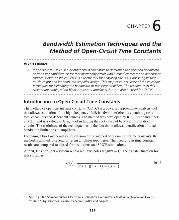
127
C H A P T E R 6Bandwidth Estimation Techniques and the
Method of Open-Circuit Time Constants
Introduction to Open-Circuit Time ConstantsThe method of open-circuit time constants (OCTC) is a powerful approximate analysis tool that allows estimation of the high-frequency –3dB bandwidth of circuits containing resis-tors, capacitors and dependent sources. The method was developed by R. B. Adler and others at MIT.1 and is a valuable design tool in fi nding the root cause of bandwidth limitation in circuits. The usefulness of the technique lies in the fact that it allows identifi cation of local bandwidth limitations in amplifi ers.
Following a brief mathematical discussion of the method of open-circuit time constants, the method is applied to several different amplifi er topologies. The open-circuit time constant results are compared to closed-form solutions and SPICE simulations.
At fi rst, let’s consider a system with n real-axis poles (Figure 6-1). The transfer function for this system is:
( )( )( ) ( )1 2
1
1 1 1n
H ss s sτ τ τ
=+ + +
[6-1]
In This Chapter
It’s possible to use PSPICE or other circuit simulators to determine the gain and bandwidth of transistor amplifi ers, or for that matter any circuit with lumped elements and dependent sources. However, while PSPICE is a useful tool for analyzing circuits, it doesn’t give that much insight and intuition into amplifi er design. This chapter covers “back of the envelope” techniques for estimating the bandwidth of transistor amplifi ers. The techniques in this chapter are employed on bipolar transistor amplifi ers, but can also be used for CMOS.
1 See, e.g., the Semiconductor Electronics Education Committee’s Multistage Transistor Circuits, volume 5, by Thornton, Searle, Pederson, Adler and Angelo.
Thompson Book.indb 127 3/20/2006 11:34:36 AM
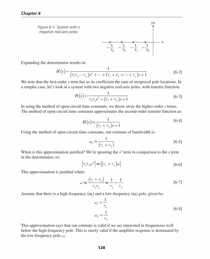
Chapter 6
128
Expanding the denominator results in:
( )( ) ( )1 2 1 2
1
1nn n
H ss sτ τ τ τ τ τ
=+ + + + + +
[6-2]
We note that the fi rst-order s term has as its coeffi cient the sum of reciprocal pole locations. In a simpler case, let’s look at a system with two negative real-axis poles, with transfer function:
( )( )2
1 2 1 2
1
1H s
s sτ τ τ τ=
+ + + [6-3]
In using the method of open-circuit time constants, we throw away the higher-order s terms. The method of open-circuit time constants approximates the second-order transfer function as:
( )( )1 2
1
1H s
sτ τ≈
+ + [6-4]
Using the method of open-circuit time constants, our estimate of bandwidth is:
( )1 2
1hω
τ τ≈
+ [6-5]
When is this approximation justifi ed? We’re ignoring the s2 term in comparison to the s term in the denominator, or:
( )21 2 1 2τ τ ω τ τ ω+ [6-6]
This approximation is justifi ed when:
( )1 2
1 2 1 2
1 1τ τω
τ τ τ τ
++ [6-7]
Assume that there is a high-frequency (ωh) and a low-frequency (ωl) pole, given by:
1
2
1
1
l
h
ωτ
ωτ
=
= [6-8]
This approximation says that our estimate is valid if we are interested in frequencies well below the high-frequency pole. This is surely valid if the amplifi er response is dominated by the low-frequency pole ωl.
σ
ωj
xxx
τn– 1
x
τ2– 1
τ1– 1
τ3– 1
Figure 6-1: System with n negative real-axis poles.
Thompson Book.indb 128 3/20/2006 11:34:37 AM
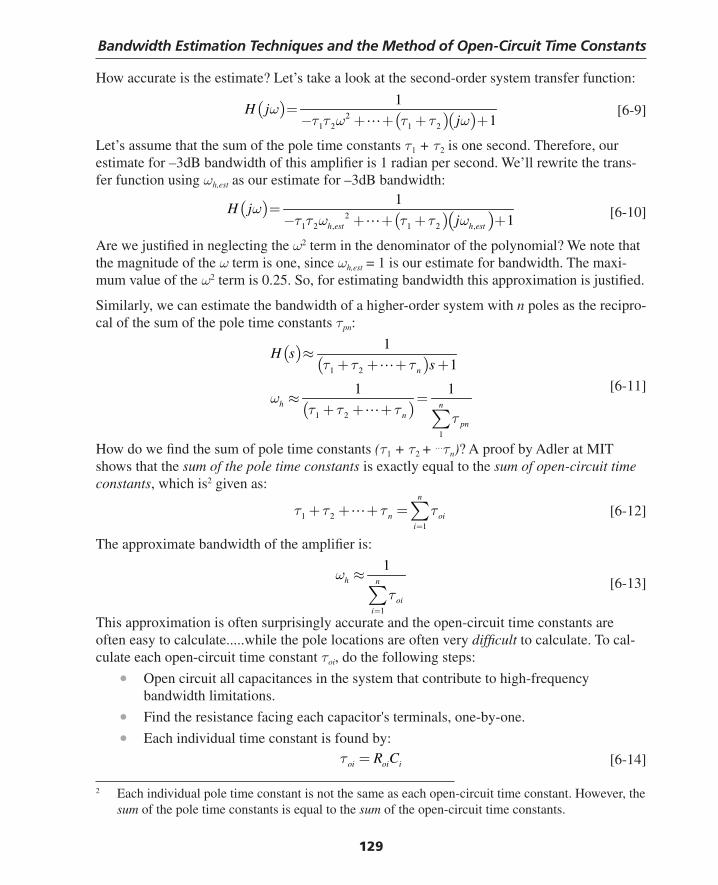
Bandwidth Estimation Techniques and the Method of Open-Circuit Time Constants
129
How accurate is the estimate? Let’s take a look at the second-order system transfer function:
( )( )( )2
1 2 1 2
1
1H j
jω
τ τ ω τ τ ω=
− + + + + [6-9]
Let’s assume that the sum of the pole time constants τ1 + τ2 is one second. Therefore, our estimate for –3dB bandwidth of this amplifi er is 1 radian per second. We’ll rewrite the trans-fer function using ωh,est as our estimate for –3dB bandwidth:
( )( )( )2
1 2 , 1 2 ,
1
1h est h est
H jj
ωτ τ ω τ τ ω
=− + + + + [6-10]
Are we justifi ed in neglecting the ω2 term in the denominator of the polynomial? We note that the magnitude of the ω term is one, since ωh,est = 1 is our estimate for bandwidth. The maxi-mum value of the ω2 term is 0.25. So, for estimating bandwidth this approximation is justifi ed.
Similarly, we can estimate the bandwidth of a higher-order system with n poles as the recipro-cal of the sum of the pole time constants τpn:
( )( )
( )
1 2
1 2
1
1
1
1 1n
h nn
pn
H ssτ τ τ
ωτ τ τ τ
≈+ + + +
≈ =+ + + ∑
[6-11]
How do we fi nd the sum of pole time constants (τ1 + τ2 + …τn)? A proof by Adler at MIT shows that the sum of the pole time constants is exactly equal to the sum of open-circuit time constants, which is2 given as:
1 21
n
n oii
τ τ τ τ=
+ + + = ∑ [6-12]
The approximate bandwidth of the amplifi er is:
1
1h n
oii
ωτ
=
≈
∑ [6-13]
This approximation is often surprisingly accurate and the open-circuit time constants are often easy to calculate.....while the pole locations are often very diffi cult to calculate. To cal-culate each open-circuit time constant τoi, do the following steps:
• Open circuit all capacitances in the system that contribute to high-frequency bandwidth limitations.
• Find the resistance facing each capacitor's terminals, one-by-one.
• Each individual time constant is found by:
oi oi iR Cτ = [6-14]
2 Each individual pole time constant is not the same as each open-circuit time constant. However, the sum of the pole time constants is equal to the sum of the open-circuit time constants.
Thompson Book.indb 129 3/20/2006 11:34:38 AM
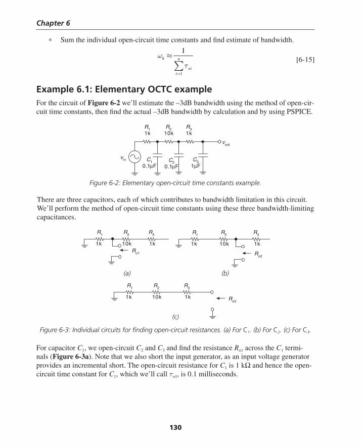
Chapter 6
130
• Sum the individual open-circuit time constants and fi nd estimate of bandwidth.
1
1h n
oii
ωτ
=
≈
∑ [6-15]
Example 6.1: Elementary OCTC exampleFor the circuit of Figure 6-2 we’ll estimate the –3dB bandwidth using the method of open-cir-cuit time constants, then fi nd the actual –3dB bandwidth by calculation and by using PSPICE.
There are three capacitors, each of which contributes to bandwidth limitation in this circuit. We’ll perform the method of open-circuit time constants using these three bandwidth-limiting capacitances.
vin
R11k
R210k
R31k
C10.1μF
vout
C20.1μF
C31μF
R1 R2 R3
1k 10k 1kRo1 Ro2
R1 R2 R3
1k 10k 1k
R1 R2 R3
1k 10k 1k Ro3
Figure 6-2: Elementary open-circuit time constants example.
(a) (b)
(c)
Figure 6-3: Individual circuits for fi nding open-circuit resistances. (a) For C1. (b) For C2. (c) For C3.
For capacitor C1, we open-circuit C2 and C3 and fi nd the resistance Ro1 across the C1 termi-nals (Figure 6-3a). Note that we also short the input generator, as an input voltage generator provides an incremental short. The open-circuit resistance for C1 is 1 kΩ and hence the open-circuit time constant for C1, which we’ll call τo1, is 0.1 milliseconds.
Thompson Book.indb 130 3/20/2006 11:34:39 AM
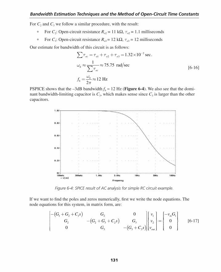
Bandwidth Estimation Techniques and the Method of Open-Circuit Time Constants
131
For C2 and C3 we follow a similar procedure, with the result:
• For C2: Open-circuit resistance Ro2 = 11 kΩ, τo2 = 1.1 milliseconds
• For C3: Open-circuit resistance Ro3 = 12 kΩ, τo3 = 12 milliseconds
Our estimate for bandwidth of this circuit is as follows:
21 2 3 1.32 10 sec.
175.75 rad sec
12 Hz2
oc o o o
hoc
hhf
τ τ τ τ
ωτ
ωπ
−= + + = ×
≈ ≈
= ≈
∑
∑ [6-16]
PSPICE shows that the –3dB bandwidth fh ≈ 12 Hz (Figure 6-4). We also see that the domi-nant bandwidth-limiting capacitor is C3, which makes sense since C3 is larger than the other capacitors.
Figure 6-4: SPICE result of AC analysis for simple RC circuit example.
If we want to fi nd the poles and zeros numerically, fi rst we write the node equations. The node equations for this system, in matrix form, are:
( )( )
( )
1 2 1 2 1 1
2 2 3 2 3 2
3 3 3
0
0
0 0
in
out
G G C s G v v G
G G G C s G v
G G C s v
⎡ ⎤ ⎧ ⎫ ⎧ ⎫− + + −⎪ ⎪ ⎪ ⎪⎪ ⎪ ⎪ ⎪⎢ ⎥⎪ ⎪ ⎪ ⎪⎪ ⎪ ⎪ ⎪⎢ ⎥− + + =⎨ ⎬ ⎨ ⎬⎢ ⎥⎪ ⎪ ⎪ ⎪⎪ ⎪ ⎪ ⎪⎢ ⎥− + ⎪ ⎪ ⎪ ⎪⎢ ⎥⎪ ⎪ ⎪ ⎪⎩ ⎭ ⎩ ⎭⎣ ⎦
[6-17]
Thompson Book.indb 131 3/20/2006 11:34:40 AM
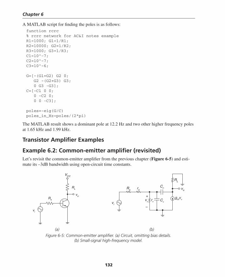
Chapter 6
132
A MATLAB script for fi nding the poles is as follows:function rcrc% rcrc network for AC&I notes exampleR1=1000; G1=1/R1;R2=10000; G2=1/R2;R3=1000; G3=1/R3;C1=10^-7;C2=10^-7;C3=10^-6;
G=[-(G1+G2) G2 0; G2 -(G2+G3) G3; 0 G3 -G3];C=[-C1 0 0; 0 -C2 0; 0 0 -C3];
poles=-eig(G/C)poles_in_Hz=poles/(2*pi)
The MATLAB result shows a dominant pole at 12.2 Hz and two other higher frequency poles at 1.65 kHz and 1.99 kHz.
Transistor Amplifi er Examples
Example 6.2: Common-emitter amplifi er (revisited)Let’s revisit the common-emitter amplifi er from the previous chapter (Figure 6-5) and esti-mate its –3dB bandwidth using open-circuit time constants.
(a) (b)
VCC
vi
voRs
RL
+
–
rx
rπ Cπ
Cμ
gmvπvπ
vo
RL
Rs
vi
Figure 6-5: Common-emitter amplifi er. (a) Circuit, omitting bias details. (b) Small-signal high-frequency model.
Thompson Book.indb 132 3/20/2006 11:34:40 AM
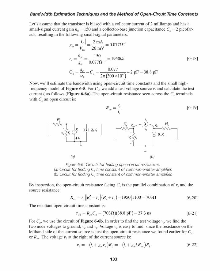
Bandwidth Estimation Techniques and the Method of Open-Circuit Time Constants
133
Let’s assume that the transistor is biased with a collector current of 2 milliamps and has a small-signal current gain hfe = 150 and a collector-base junction capacitance Cμ = 2 picofar-ads, resulting in the following small-signal parameters:
( )
1
1
6
2 mA0.077
26 mV
1501950
0.077
0.077C 2 pF 38.8 pF
2 300 10
Cm
TH
fe
m
m
T
Ig
V
hr
g
gC
π
π μω π
−
−
= = =
= = =
= − = − =×
Ω
ΩΩ
[6-18]
Now, we’ll estimate the bandwidth using open-circuit time constants and the small high- frequency model of Figure 6-5. For Cπ, we add a test voltage source vt and calculate the test current it as follows (Figure 6-6a). The open-circuit resistance seen across the Cπ terminals with Cμ an open circuit is:
to
t
vR
iπ = [6-19]
(a) (b)
Figure 6-6: Circuits for fi nding open-circuit resistances. (a) Circuit for fi nding Cπ time constant of common-emitter amplifi er. (b) Circuit for fi nding Cμ time constant of common-emitter amplifi er.
g vm π+–
vtrπvπ
+
– it
Rs'
g vm π
vt
rπvπ
+
–
itRs
'
+ –RLvbva
By inspection, the open-circuit resistance facing Cπ is the parallel combination of rπ and the source resistance:
( ) 1950 1100 703o s s xR r R r R rπ π π′= = + = = Ω [6-20]
The resultant open-circuit time constant is:
( )( )703 38.8 pF 27.3 nso oR Cπ π πτ = = =Ω [6-21]
For Cμ, we use the circuit of Figure 6-6b. In order to fi nd the test voltage vt, we fi nd the two node voltages to ground, va and vb. Voltage va is easy to fi nd, since the resistance on the lefthand side of the current source is just the open-circuit resistance we found earlier for Cπ, or Roπ. The voltage vb at the right of the current source is:
( ) ( )b t m L t m t o Lv i g v R i g i R Rπ π= − + = − + [6-22]
Thompson Book.indb 133 3/20/2006 11:34:41 AM
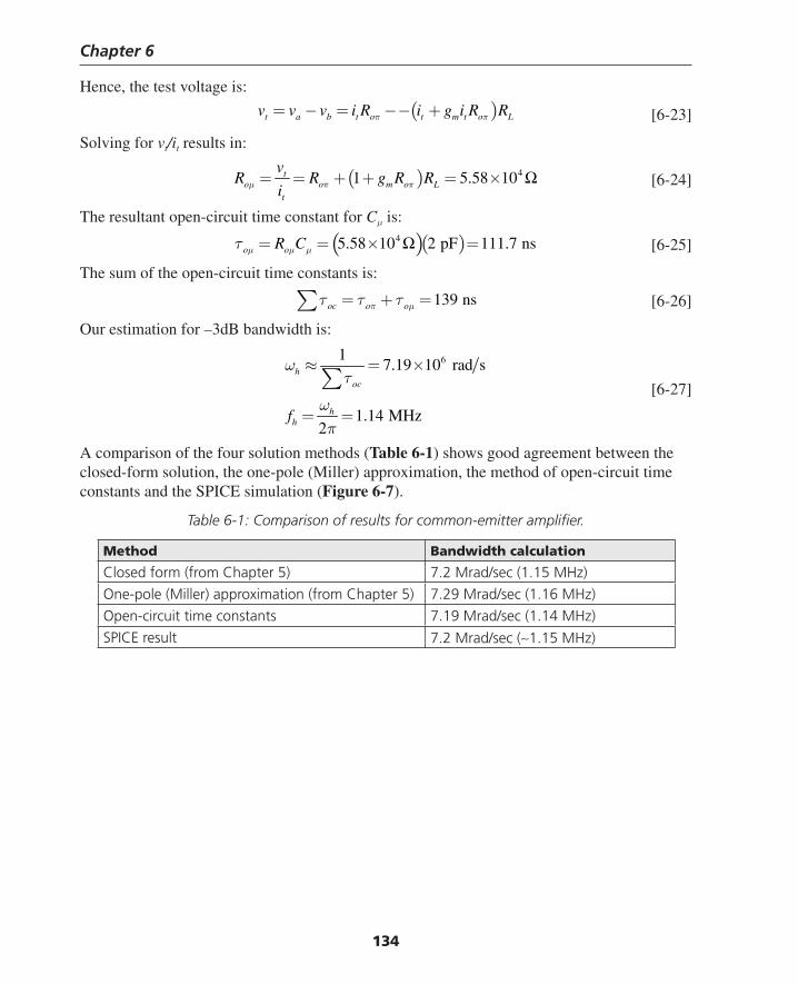
Chapter 6
134
Hence, the test voltage is:
( )t a b t o t m t o Lv v v i R i g i R Rπ π= − = −− + [6-23]
Solving for vt/it results in:
( ) 41 5.58 10to o m o L
t
vR R g R R
iμ π π= = + + = × Ω [6-24]
The resultant open-circuit time constant for Cμ is:
( )( )45.58 10 2 pF 111.7 nso oR Cμ μ μτ = = × =Ω [6-25]
The sum of the open-circuit time constants is:
139 nsoc o oπ μτ τ τ= + =∑ [6-26]
Our estimation for –3dB bandwidth is:
617.19 10 rad s
1.14 MHz2
hoc
hhf
ωτ
ωπ
≈ = ×
= =
∑ [6-27]
A comparison of the four solution methods (Table 6-1) shows good agreement between the closed-form solution, the one-pole (Miller) approximation, the method of open-circuit time constants and the SPICE simulation (Figure 6-7).
Table 6-1: Comparison of results for common-emitter amplifi er.
Method Bandwidth calculation
Closed form (from Chapter 5) 7.2 Mrad/sec (1.15 MHz)
One-pole (Miller) approximation (from Chapter 5) 7.29 Mrad/sec (1.16 MHz)
Open-circuit time constants 7.19 Mrad/sec (1.14 MHz)
SPICE result 7.2 Mrad/sec (∼1.15 MHz)
Thompson Book.indb 134 3/20/2006 11:34:42 AM
Bandwidth Estimation Techniques and the Method of Open-Circuit Time Constants
135
Figure 6-7: SPICE result for common-emitter amplifi er.
Using the common-emitter amplifi er result as an OCTC sanity checkWe’re now in a position to use the closed-form result of the previous chapter as a sanity check for the open-circuit time constants method. The closed-form transfer function for the com-mon-emitter amplifi er, repeated here for the reader’s convenience, is:
( )( ) ( )2
1
11
o s mm L
Li sL m s
s s
Cs
v s G gg R
R C Cv s G gs R g g G C C C S
G g G g
μ
π μππ μ π μ
π π
⎡ ⎤⎢ ⎥−⎢ ⎥′ ⎢ ⎥= − ⎢ ⎥′ + ⎡ ⎤⎢ ⎥′+ + + + + +⎢ ⎥⎣ ⎦⎢ ⎥′ ′+ +⎣ ⎦
[6-28]
Note that coeffi cient of the s term is:
( )1L m s
s
R g g G C C CG g π μ π μ
π
⎡ ⎤′+ + + +⎢ ⎥⎣ ⎦′ + [6-29]
We’ll regroup the terms of the “s” coeffi cient so we can see the terms associated with Cπ and Cμ individually.
( )1
1
L m ss s s
m LL
s s
CCR g g G C
G g G g G g
C g RC R C
G g G g
μππ μ
π π π
πμ μ
π π
⎡ ⎤′+ + + +⎢ ⎥⎣ ⎦′ ′ ′+ + +
⎛ ⎞+ ⎟⎜ ⎟≈ + +⎜ ⎟⎜ ⎟⎜′ ′+ +⎝ ⎠
[6-30]
Thompson Book.indb 135 3/20/2006 11:34:42 AM
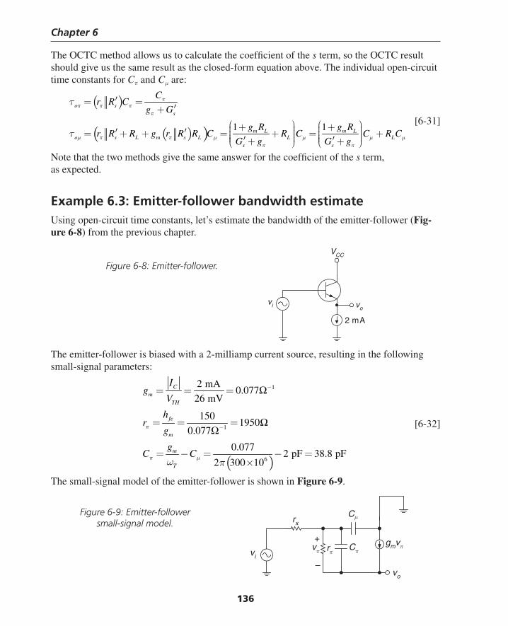
Chapter 6
136
The OCTC method allows us to calculate the coeffi cient of the s term, so the OCTC result should give us the same result as the closed-form equation above. The individual open-circuit time constants for Cπ and Cμ are:
( )
( )( ) 1 1
o ss
m L m Lo s L m s L L L
s s
Cr R C
g G
g R g Rr R R g r R R C R C C R C
G g G g
ππ π π
π
μ π π μ μ μ μπ π
τ
τ
′= =′+
⎛ ⎞ ⎛ ⎞+ +⎟ ⎟⎜ ⎜′ ′ ⎟ ⎟= + + = + = +⎜ ⎜⎟ ⎟⎜ ⎜⎟ ⎟⎜ ⎜′ ′+ +⎝ ⎠ ⎝ ⎠
[6-31]
Note that the two methods give the same answer for the coeffi cient of the s term, as expected.
Example 6.3: Emitter-follower bandwidth estimateUsing open-circuit time constants, let’s estimate the bandwidth of the emitter-follower (Fig-ure 6-8) from the previous chapter.
VCC
2 mA
vi vo
The emitter-follower is biased with a 2-milliamp current source, resulting in the following small-signal parameters:
( )
1
1
6
2 mA0.077
26 mV
1501950
0.077
0.0772 pF 38.8 pF
2 300 10
Cm
TH
fe
m
m
T
Ig
V
hr
g
gC C
π
π μω π
−
−
= = =
= = =
= − = − =×
Ω
ΩΩ
[6-32]
The small-signal model of the emitter-follower is shown in Figure 6-9.
Figure 6-8: Emitter-follower.
+
–
rx
rπCπ
Cμ
gmvπvπ
vo
vi
Figure 6-9: Emitter-follower small-signal model.
Thompson Book.indb 136 3/20/2006 11:34:43 AM
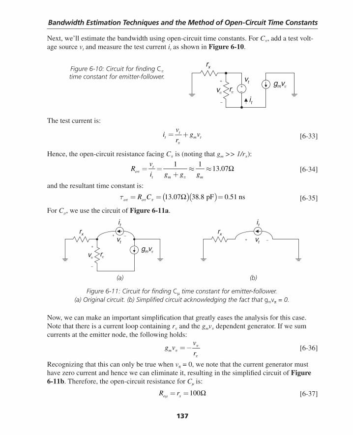
Bandwidth Estimation Techniques and the Method of Open-Circuit Time Constants
137
Next, we’ll estimate the bandwidth using open-circuit time constants. For Cπ, add a test volt-age source vt and measure the test current it as shown in Figure 6-10.
g vm π+–
vt
rπvπ
+
– it
rx
The test current is:
t
t m t
vi g v
rπ
= + [6-33]
Hence, the open-circuit resistance facing Cπ is (noting that gm >> 1/rπ):
1 1
13.07to
t m m
vR
i g g gππ
= = ≈ ≈+
Ω [6-34]
and the resultant time constant is:
( )( )13.07 38.8 pF 0.51 nso oR Cπ π πτ = = =Ω [6-35]
For Cμ, we use the circuit of Figure 6-11a.
(a) (b)
Figure 6-11: Circuit for fi nding Cμ time constant for emitter-follower. (a) Original circuit. (b) Simplifi ed circuit acknowledging the fact that gmvπ = 0.
g vm π
vt
rπvπ
+
–
itrx + –
vt
itrx
+ –
Figure 6-10: Circuit for fi nding Cπ time constant for emitter-follower.
Now, we can make an important simplifi cation that greatly eases the analysis for this case. Note that there is a current loop containing rπ and the gmvπ dependent generator. If we sum currents at the emitter node, the following holds:
m
vg v
rπ
ππ
= − [6-36]
Recognizing that this can only be true when vπ = 0, we note that the current generator must have zero current and hence we can eliminate it, resulting in the simplifi ed circuit of Figure 6-11b. Therefore, the open-circuit resistance for Cµ is:
100o xR rμ = = Ω [6-37]
Thompson Book.indb 137 3/20/2006 11:34:44 AM
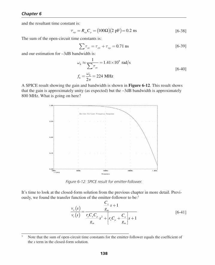
Chapter 6
138
and the resultant time constant is:
( )( )100 2 pF 0.2 nso oR Cμ μ μτ = = =Ω [6-38]
The sum of the open-circuit time constants is:
0.71 nsoc o oπ μτ τ τ= + =∑ [6-39]
and our estimation for –3dB bandwidth is:
911.41 10 rad s
224 MHz2
hoc
hhf
ωτ
ωπ
≈ = ×
= =
∑ [6-40]
A SPICE result showing the gain and bandwidth is shown in Figure 6-12. This result shows that the gain is approximately unity (as expected) but the –3dB bandwidth is approximately 800 MHz. What is going on here?
Figure 6-12: SPICE result for emitter-follower.
It’s time to look at the closed-form solution from the previous chapter in more detail. Previ-ously, we found the transfer function of the emitter-follower to be:3
( )( ) 2
1
1
o m
xix
m m
Cs
v s g
r C Cv s Cs r C s
g g
π
π μ πμ
+=
⎡ ⎤⎢ ⎥+ + +⎢ ⎥⎣ ⎦
[6-41]
3 Note that the sum of open-circuit time constants for the emitter-follower equals the coeffi cient of the s term in the closed-form solution.
Thompson Book.indb 138 3/20/2006 11:34:45 AM
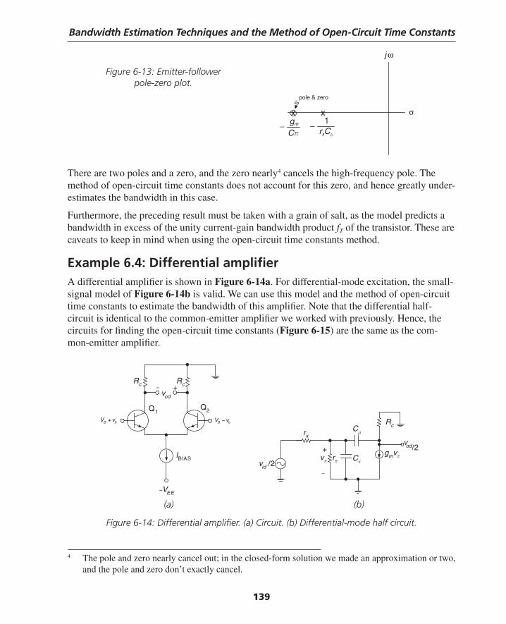
Bandwidth Estimation Techniques and the Method of Open-Circuit Time Constants
139
There are two poles and a zero, and the zero nearly4 cancels the high-frequency pole. The method of open-circuit time constants does not account for this zero, and hence greatly under-estimates the bandwidth in this case.
Furthermore, the preceding result must be taken with a grain of salt, as the model predicts a bandwidth in excess of the unity current-gain bandwidth product fT of the transistor. These are caveats to keep in mind when using the open-circuit time constants method.
Example 6.4: Differential amplifi erA differential amplifi er is shown in Figure 6-14a. For differential-mode excitation, the small-signal model of Figure 6-14b is valid. We can use this model and the method of open-circuit time constants to estimate the bandwidth of this amplifi er. Note that the differential half-circuit is identical to the common-emitter amplifi er we worked with previously. Hence, the circuits for fi nding the open-circuit time constants (Figure 6-15) are the same as the com-mon-emitter amplifi er.
4 The pole and zero nearly cancel out; in the closed-form solution we made an approximation or two, and the pole and zero don’t exactly cancel.
σ
ωj
xx1−
Cπgm− rxCμ
pole & zero
Figure 6-13: Emitter-follower pole-zero plot.
−VEE
IBIAS
V vB b+ V vB b−
Q1Q2
vod
RcRc +−
+
−
rx
rπ Cπ
Cμ
gmvπvπvid /2
Rc
vod/2
(a) (b)
Figure 6-14: Differential amplifi er. (a) Circuit. (b) Differential-mode half circuit.
Thompson Book.indb 139 3/20/2006 11:34:45 AM
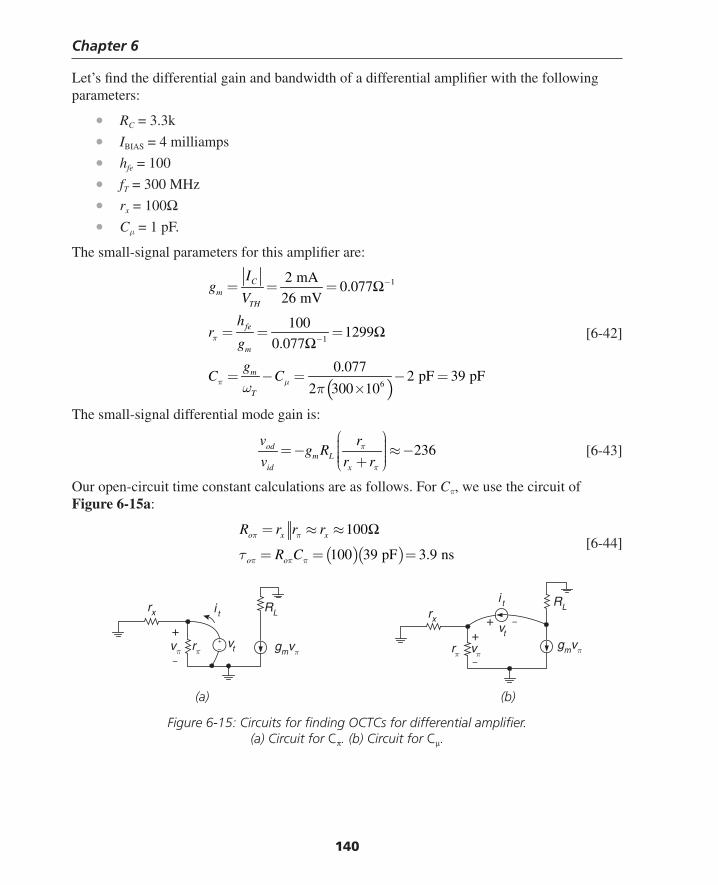
Chapter 6
140
Let’s fi nd the differential gain and bandwidth of a differential amplifi er with the following parameters:
• RC = 3.3k
• IBIAS = 4 milliamps
• hfe = 100
• fT = 300 MHz
• rx = 100Ω• Cμ = 1 pF.
The small-signal parameters for this amplifi er are:
( )
1
1
6
2 mA0.077
26 mV
1001299
0.077
0.0772 pF 39 pF
2 300 10
Cm
TH
fe
m
m
T
Ig
V
hr
g
gC C
π
π μω π
−
−
= = =
= = =
= − = − =×
Ω
ΩΩ
[6-42]
The small-signal differential mode gain is:
236odm L
id x
v rg R
v r rπ
π
⎛ ⎞⎟⎜ ⎟= − ≈ −⎜ ⎟⎜ ⎟⎜ +⎝ ⎠ [6-43]
Our open-circuit time constant calculations are as follows. For Cπ, we use the circuit of Figure 6-15a:
( )( )
100
100 39 pF 3.9 ns
o x x
o o
R r r r
R C
π π
π π πτ
= ≈ ≈
= = =
Ω [6-44]
rx
gmvπvt
RL
+
−
rπvπ
i t
+–
+ −
vπrπgmvπ
i t RLrx
−
vt+
(a) (b)
Figure 6-15: Circuits for fi nding OCTCs for differential amplifi er. (a) Circuit for Cπ. (b) Circuit for Cμ.
Thompson Book.indb 140 3/20/2006 11:34:46 AM
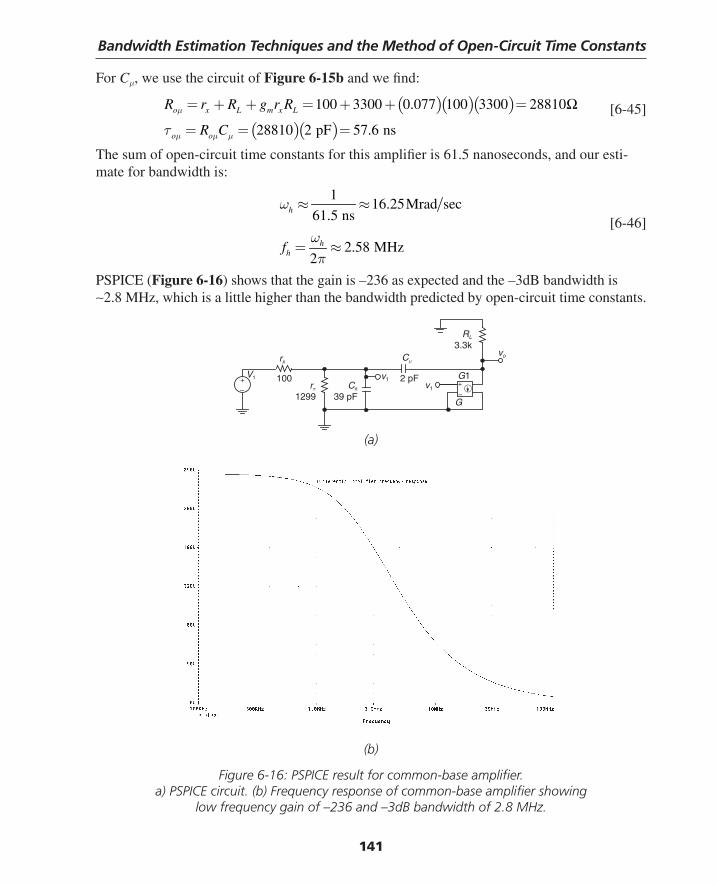
Bandwidth Estimation Techniques and the Method of Open-Circuit Time Constants
141
For Cμ, we use the circuit of Figure 6-15b and we fi nd:
( )( )( )( )( )
100 3300 0.077 100 3300 28810
28810 2 pF 57.6 ns
o x L m x L
o o
R r R g r R
R C
μ
μ μ μτ
= + + = + + =
= = =
Ω [6-45]
The sum of open-circuit time constants for this amplifi er is 61.5 nanoseconds, and our esti-mate for bandwidth is:
116.25Mrad sec
61.5 ns
2.58 MHz2
h
hhf
ω
ωπ
≈ ≈
= ≈
[6-46]
PSPICE (Figure 6-16) shows that the gain is –236 as expected and the –3dB bandwidth is ∼2.8 MHz, which is a little higher than the bandwidth predicted by open-circuit time constants.
(a)
+–
V1
rx Cμ
RL
3.3kvo
G
G1v1v1
2 pFCπ
39 pFrπ
1299
100+
–
(b)
Figure 6-16: PSPICE result for common-base amplifi er. a) PSPICE circuit. (b) Frequency response of common-base amplifi er showing
low frequency gain of –236 and –3dB bandwidth of 2.8 MHz.
Thompson Book.indb 141 3/20/2006 11:34:46 AM
Chapter 6
142
Example 6.5: Design case study using open-circuit time constantsIn the previous examples, we used open-circuit time constants to analyze the bandwidth of some circuits. In the following example, we’ll use open-circuit time constants as a tool in an iterative design exercise. Let’s design a transistor amplifi er to meet the following gain and bandwidth specifi cations:
• Magnitude of midband gain: |Av| : > 100
• Input source resistance: Rs = 2 kΩ (high impedance source, such as a microphone)
• Load capacitance: CL = 10 pF (scope probe, stray capacitance, etc.)
• –3dB bandwidth: fh > 10 MHz
• Transistor parameters: hfe = 150; fT = 300 MHz; Cμ ≈ 2 pF
As an initial guess at a circuit topology, let’s consider the AC-coupled common-emitter amplifi er of Figure 6-17a. The Bode plot of this amplifi er looks qualitatively like that in Figure 6-17b. The high-frequency rolloff is due to the bandwidth-limiting effects of transis-tor internal capacitances Cπ and Cμ. The low-frequency rolloff is due to the coupling capacitor CC and the emitter bypass capacitor CE.5 In the next chapter, we’ll estimate the low-frequency breakpoint fL using the method of short-circuit time constants. In this section, we’ll estimate the high-frequency rolloff fh using open-circuit time constants.
TRY #1: Common-emitter amplifi erFirst, let’s arbitrarily assume that the collector current of the transistor is 2 milliamps.6 Other small-signal parameters are:
( )
1 11
11 1
1
11 1 6
2 mA0.077
26 mV
1501948
0.077
0.0772 pF 39 pF
2 300 10
Cm
TH
fe
m
m
T
Ig
V
hr
g
gC C
π
π μω π
−
−
= = =
= = =
= − = − =×
Ω
ΩΩ
[6-47]
5 We’ll assume that Cc and CE are so large that the low-frequency breakpoint fL is well below the high-frequency breakpoint fh.
6 We can easily bias this transistor at a collector current of 2 milliamps by carefully designing the values of RB1, RB2 and RE as shown in the previous discussions on transistor biasing.
Thompson Book.indb 142 3/20/2006 11:34:47 AM
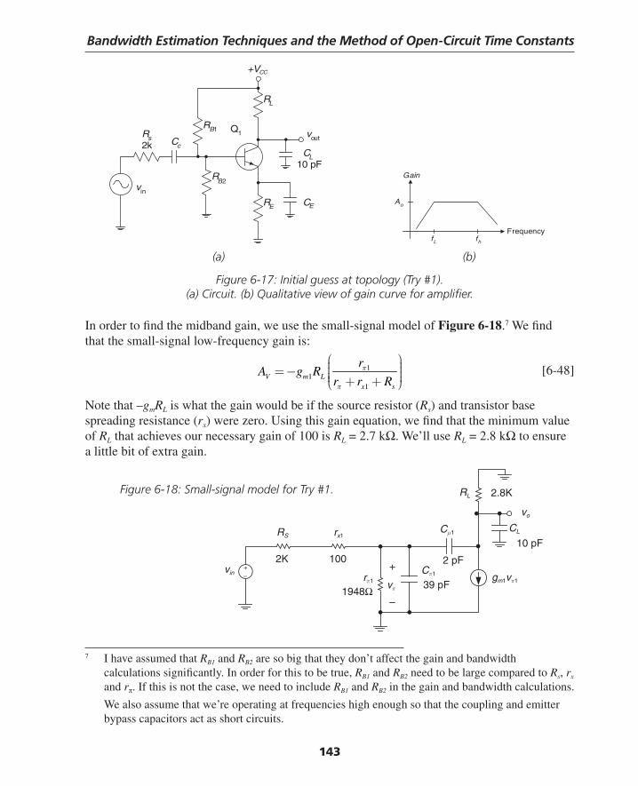
Bandwidth Estimation Techniques and the Method of Open-Circuit Time Constants
143
(a) (b)
Figure 6-17: Initial guess at topology (Try #1). (a) Circuit. (b) Qualitative view of gain curve for amplifi er.
In order to fi nd the midband gain, we use the small-signal model of Figure 6-18.7 We fi nd that the small-signal low-frequency gain is:
11
1V m L
x s
rA g R
r r Rπ
π
⎛ ⎞⎟⎜ ⎟= − ⎜ ⎟⎜ ⎟⎜ + +⎝ ⎠ [6-48]
Note that –gmRL is what the gain would be if the source resistor (Rs) and transistor base spreading resistance (rx) were zero. Using this gain equation, we fi nd that the minimum value of RL that achieves our necessary gain of 100 is RL = 2.7 kΩ. We’ll use RL = 2.8 kΩ to ensure a little bit of extra gain.
Rs2k
vin
RB1
RB2
Cc
RL
+VCC
RE
vout
CL10 pF
CE
Q1
fhfL
Ao
Frequency
Gain
7 I have assumed that RB1 and RB2 are so big that they don’t affect the gain and bandwidth calculations signifi cantly. In order for this to be true, RB1 and RB2 need to be large compared to Rs, rx and rπ. If this is not the case, we need to include RB1 and RB2 in the gain and bandwidth calculations.
We also assume that we’re operating at frequencies high enough so that the coupling and emitter bypass capacitors act as short circuits.
2K 100
RS rx1
vinrπ1
1948Ωvπ
+
–
Cμ1
gm1vπ1
2 pF
39 pFCπ1
10 pF
vo
RL
CL
2.8K
+–
Figure 6-18: Small-signal model for Try #1.
Thompson Book.indb 143 3/20/2006 11:34:48 AM
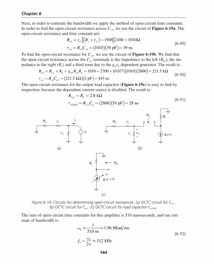
Chapter 6
144
Next, in order to estimate the bandwidth we apply the method of open-circuit time constants. In order to fi nd the open-circuit resistance across Cπ1, we use the circuit of Figure 6-19a. The open-circuit resistance and time constant are:
( )
( )( )1 1 1
1 1 1
1948 2100 1010
1010 39 pF 39 ns
s xR r R r
R C
π π
π π πτ
= + = =
= = =
Ω [6-49]
To fi nd the open-circuit resistance for Cμ1, we use the circuit of Figure 6-19b. We fi nd that the open-circuit resistance across the Cμ1 terminals is the impedance to the left (Rπ1), the im-pedance to the right (RL) and a third term due to the gmvπ dependent generator. The result is:
( )( )( )
( )( )1 1 1 1
1 1 1
1010 2700 0.077 1010 2800 221.5 k
221.5 k 2 pF 443 ns
L m LR R R g R R
R C
μ π π
μ μ μτ
= + + = + + =
= = =
Ω
Ω [6-50]
The open-circuit resistance for the output load capacitor (Figure 6-19c) is easy to fi nd by inspection, because the dependent current source is disabled. The result is:
( )( )
,
,
2.8 k
2800 10 pF 28 ns
o L L
LOAD o L L
R R
R Cτ
= =
= = =
Ω [6-51]
(a) (b)
RS rx1
rπ1vt
it
+–
RS rx1
rπ1 vπ1
+
–
RL
gm1vπ1
Rμ1
RL
gmvπ = 0
Ro,L
o
(c)
Figure 6-19: Circuits for determining open-circuit resistances. (a) OCTC circuit for Cπ1. (b) OCTC circuit for Cμ1. (c) OCTC circuit for load capacitor CLOAD.
The sum of open-circuit time constants for this amplifi er is 510 nanoseconds, and our esti-mate of bandwidth is:
11.96 Mrad sec
510 ns
312 kHz2
h
hhf
ω
ωπ
≈ ≈
= ≈
[6-52]
Thompson Book.indb 144 3/20/2006 11:34:48 AM
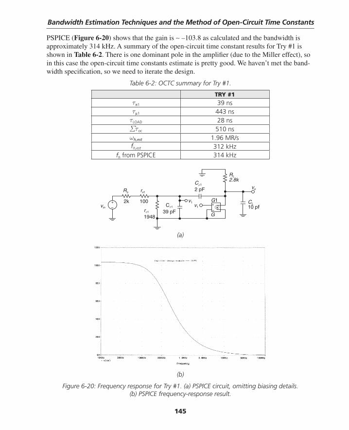
Bandwidth Estimation Techniques and the Method of Open-Circuit Time Constants
145
PSPICE (Figure 6-20) shows that the gain is ∼ –103.8 as calculated and the bandwidth is approximately 314 kHz. A summary of the open-circuit time constant results for Try #1 is shown in Table 6-2. There is one dominant pole in the amplifi er (due to the Miller effect), so in this case the open-circuit time constants estimate is pretty good. We haven’t met the band-width specifi cation, so we need to iterate the design.
Table 6-2: OCTC summary for Try #1.
TRY #1τπ1 39 nsτμ1 443 ns
τLOAD 28 ns∑τoc 510 nsωh,est 1.96 MR/sfh,est 312 kHz
fh from PSPICE 314 kHz
+–vin
rx1Rs
Cμ1
2 pF
RL2.8k
vo
G
G1v1v1Cπ1
39 pFrπ1
1948
1002k+
–
CL10 pF
(a)
(b)
Figure 6-20: Frequency response for Try #1. (a) PSPICE circuit, omitting biasing details. (b) PSPICE frequency-response result.
Thompson Book.indb 145 3/20/2006 11:34:49 AM
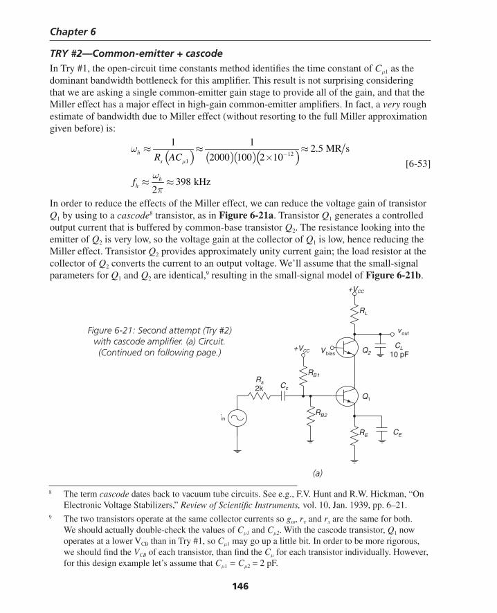
Chapter 6
146
TRY #2—Common-emitter + cascodeIn Try #1, the open-circuit time constants method identifi es the time constant of Cμ1 as the dominant bandwidth bottleneck for this amplifi er. This result is not surprising considering that we are asking a single common-emitter gain stage to provide all of the gain, and that the Miller effect has a major effect in high-gain common-emitter amplifi ers. In fact, a very rough estimate of bandwidth due to Miller effect (without resorting to the full Miller approximation given before) is:
( ) ( )( )( )121
1 12.5 MR s
2000 100 2 10
398 kHz2
h
s
hh
R AC
f
μ
ω
ωπ
−≈ ≈ ≈
×
≈ ≈
[6-53]
In order to reduce the effects of the Miller effect, we can reduce the voltage gain of transistor Q1 by using to a cascode8 transistor, as in Figure 6-21a. Transistor Q1 generates a controlled output current that is buffered by common-base transistor Q2. The resistance looking into the emitter of Q2 is very low, so the voltage gain at the collector of Q1 is low, hence reducing the Miller effect. Transistor Q2 provides approximately unity current gain; the load resistor at the collector of Q2 converts the current to an output voltage. We’ll assume that the small-signal parameters for Q1 and Q2 are identical,9 resulting in the small-signal model of Figure 6-21b.
8 The term cascode dates back to vacuum tube circuits. See e.g., F.V. Hunt and R.W. Hickman, “On Electronic Voltage Stabilizers,” Review of Scientifi c Instruments, vol. 10, Jan. 1939, pp. 6–21.
9 The two transistors operate at the same collector currents so gm, rπ and rx are the same for both. We should actually double-check the values of Cμ1 and Cμ2. With the cascode transistor, Q1 now operates at a lower VCB than in Try #1, so Cμ1 may go up a little bit. In order to be more rigorous, we should fi nd the VCB of each transistor, than fi nd the Cμ for each transistor individually. However, for this design example let’s assume that Cμ1 = Cμ2 = 2 pF.
Rs2k
v in
RB1
RB2
Cc
RL
+VCC
RE CE
Q1
Q2
vout
CL10 pF
+VCC Vbias
Figure 6-21: Second attempt (Try #2) with cascode amplifi er. (a) Circuit. (Continued on following page.)
(a)
Thompson Book.indb 146 3/20/2006 11:34:50 AM
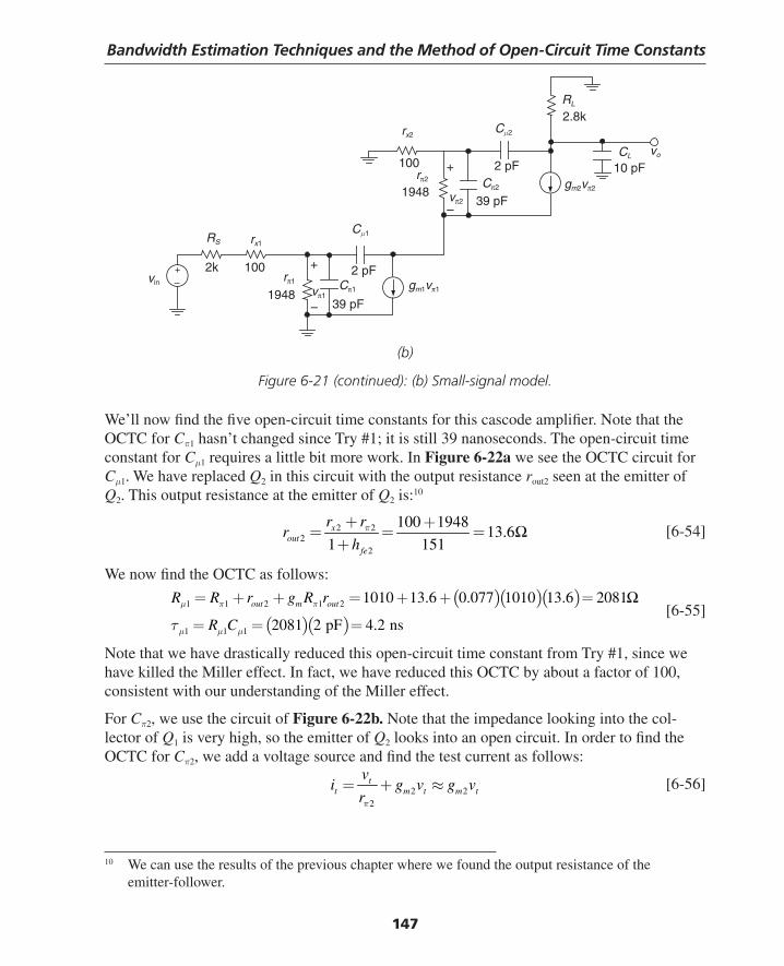
Bandwidth Estimation Techniques and the Method of Open-Circuit Time Constants
147
(b)
Figure 6-21 (continued): (b) Small-signal model.
We’ll now fi nd the fi ve open-circuit time constants for this cascode amplifi er. Note that the OCTC for Cπ1 hasn’t changed since Try #1; it is still 39 nanoseconds. The open-circuit time constant for Cμ1 requires a little bit more work. In Figure 6-22a we see the OCTC circuit for Cμ1. We have replaced Q2 in this circuit with the output resistance rout2 seen at the emitter of Q2. This output resistance at the emitter of Q2 is:10
2 22
2
100 194813.6
1 151x
outfe
r rr
hπ+ +
= = =+
Ω [6-54]
We now fi nd the OCTC as follows:
( )( )( )
( )( )1 1 2 1 2
1 1 1
1010 13.6 0.077 1010 13.6 2081
2081 2 pF 4.2 ns
out m outR R r g R r
R C
μ π π
μ μ μτ
= + + = + + =
= = =
Ω [6-55]
Note that we have drastically reduced this open-circuit time constant from Try #1, since we have killed the Miller effect. In fact, we have reduced this OCTC by about a factor of 100, consistent with our understanding of the Miller effect.
For Cπ2, we use the circuit of Figure 6-22b. Note that the impedance looking into the col-lector of Q1 is very high, so the emitter of Q2 looks into an open circuit. In order to fi nd the OCTC for Cπ2, we add a voltage source and fi nd the test current as follows:
2 22
tt m t m t
vi g v g v
rπ
= + ≈ [6-56]
+–vin
rx1RS
Cμ1
rπ1
1948
1002k
vπ1Cπ1
39 pF
2 pFgm1vπ1
Cμ2
Cπ2
rπ2
vπ2
gm2vπ2
RL
CL vo
2.8k
2 pF 10 pF
39 pF
rx2
+
–1948
100
+
–
10 We can use the results of the previous chapter where we found the output resistance of the emitter-follower.
Thompson Book.indb 147 3/20/2006 11:34:50 AM
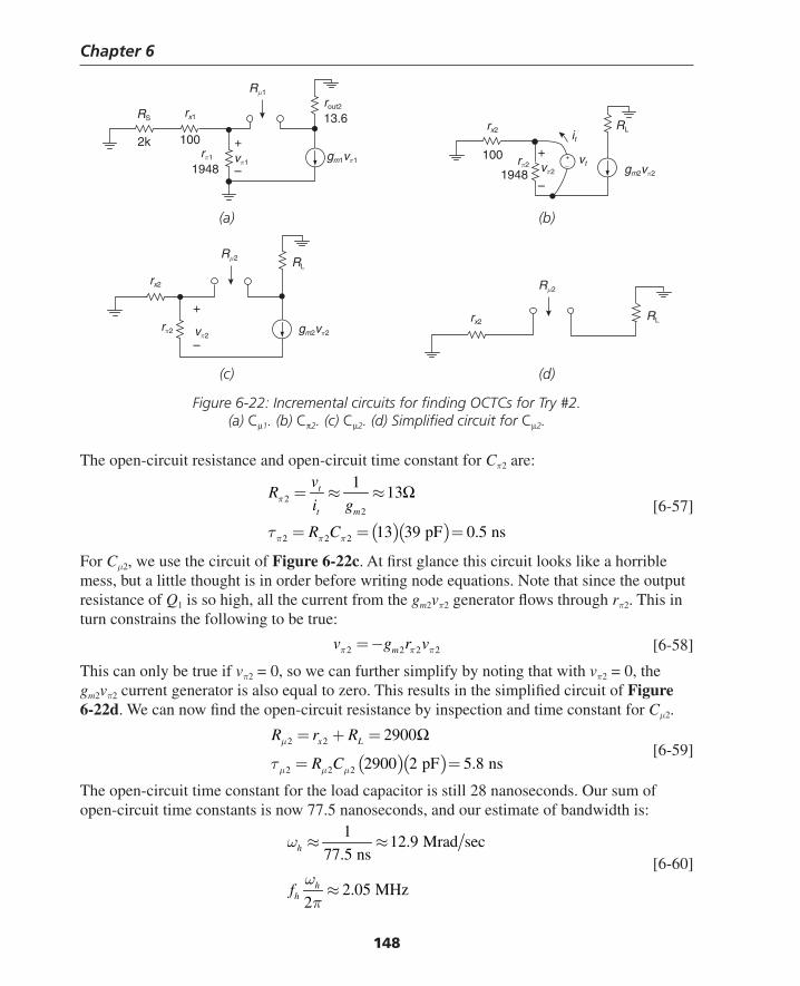
Chapter 6
148
(a) (b)
rout2
13.6
Rμ1
gm1vπ1vπ1rπ1
RS rx1
2k 100
1948
+
–gm2vπ2
RL
Rμ2
rx2
vπ2rπ2
+
–
Rμ2
rx2 RL
gm2vπ2
RL
+
–
rx2
100 rπ2 vπ21948vt
it
+–
(c) (d)
Figure 6-22: Incremental circuits for fi nding OCTCs for Try #2. (a) Cμ1. (b) Cπ2. (c) Cμ2. (d) Simplifi ed circuit for Cμ2.
The open-circuit resistance and open-circuit time constant for Cπ2 are:
( )( )
22
2 2 2
113
13 39 pF 0.5 ns
t
t m
vR
i g
R C
π
π π πτ
= ≈ ≈
= = =
Ω [6-57]
For Cμ2, we use the circuit of Figure 6-22c. At fi rst glance this circuit looks like a horrible mess, but a little thought is in order before writing node equations. Note that since the output resistance of Q1 is so high, all the current from the gm2vπ2 generator fl ows through rπ2. This in turn constrains the following to be true:
2 2 2 2mv g r vπ π π= − [6-58]
This can only be true if vπ2 = 0, so we can further simplify by noting that with vπ2 = 0, the gm2vπ2 current generator is also equal to zero. This results in the simplifi ed circuit of Figure 6-22d. We can now fi nd the open-circuit resistance by inspection and time constant for Cμ2.
( )( )
2 2
2 2 2
2900
2900 2 pF 5.8 ns
x LR r R
R C
μ
μ μ μτ
= + =
= =
Ω [6-59]
The open-circuit time constant for the load capacitor is still 28 nanoseconds. Our sum of open-circuit time constants is now 77.5 nanoseconds, and our estimate of bandwidth is:
112.9 Mrad sec
77.5 ns
2.05 MHz2
h
hhf
ω
ωπ
≈ ≈
≈
[6-60]
Thompson Book.indb 148 3/20/2006 11:34:51 AM
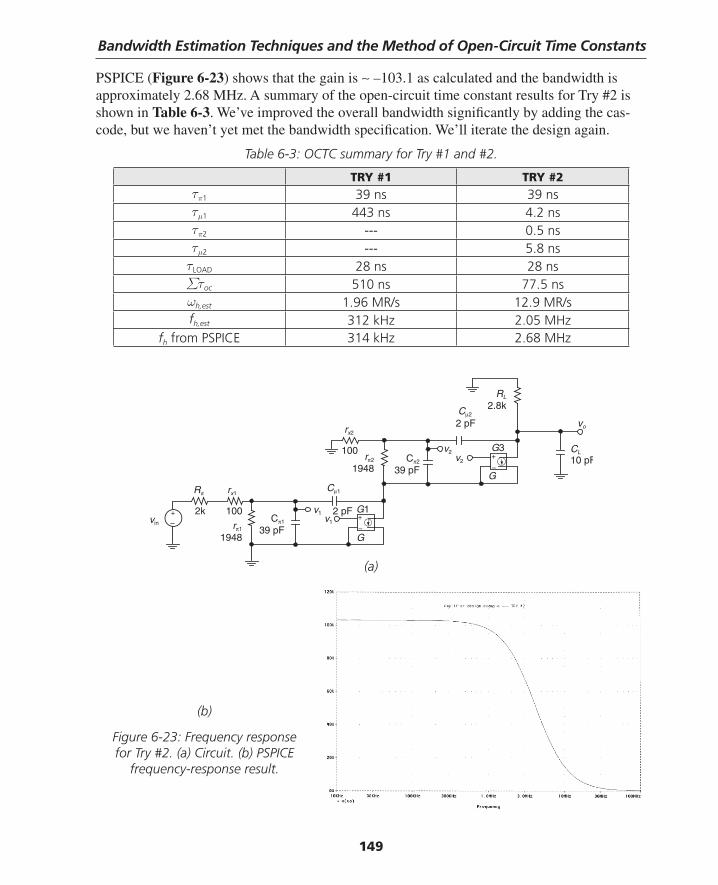
Bandwidth Estimation Techniques and the Method of Open-Circuit Time Constants
149
PSPICE (Figure 6-23) shows that the gain is ∼ –103.1 as calculated and the bandwidth is approximately 2.68 MHz. A summary of the open-circuit time constant results for Try #2 is shown in Table 6-3. We’ve improved the overall bandwidth signifi cantly by adding the cas-code, but we haven’t yet met the bandwidth specifi cation. We’ll iterate the design again.
Table 6-3: OCTC summary for Try #1 and #2.
TRY #1 TRY #2τπ1 39 ns 39 nsτμ1 443 ns 4.2 nsτπ2 --- 0.5 nsτμ2 --- 5.8 ns
τLOAD 28 ns 28 ns∑τoc 510 ns 77.5 nsωh,est 1.96 MR/s 12.9 MR/sfh,est 312 kHz 2.05 MHz
fh from PSPICE 314 kHz 2.68 MHz
(a)
v1
rx2
Cμ2
RL
2.8k
vo
G
G3v2v2
2 pF
Cπ2
39 pFrπ2
1948
100+
–
+–vin
1002k+
–v1
2 pF
Cμ1
G
G1Cπ1
39 pFrπ1
1948
rx1Rs
CL
10 pF
(b)
Figure 6-23: Frequency response for Try #2. (a) Circuit. (b) PSPICE
frequency-response result.
Thompson Book.indb 149 3/20/2006 11:34:52 AM
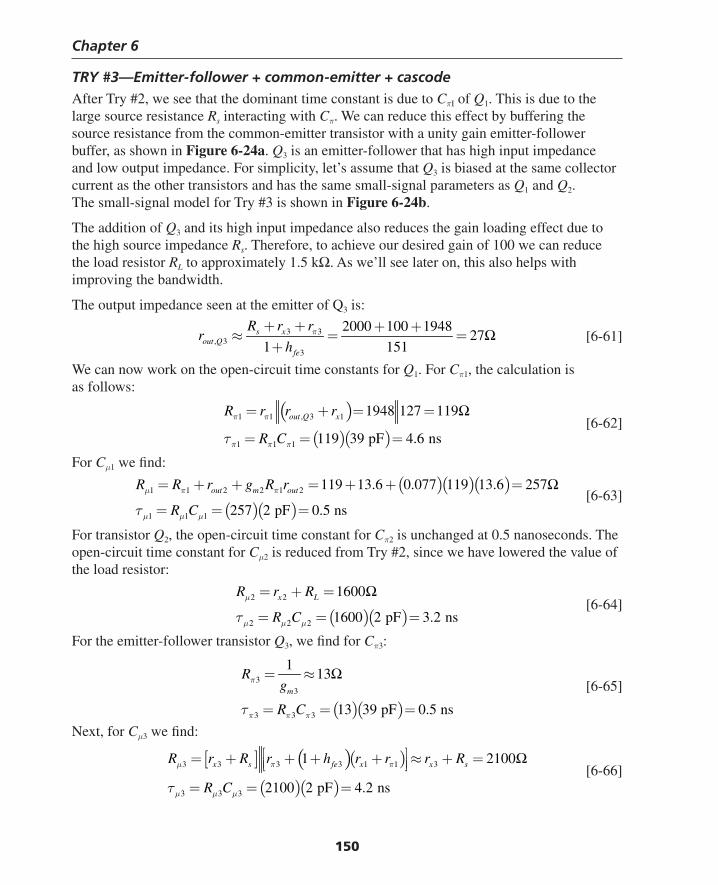
Chapter 6
150
TRY #3—Emitter-follower + common-emitter + cascodeAfter Try #2, we see that the dominant time constant is due to CπI of Q1. This is due to the large source resistance Rs interacting with Cπ. We can reduce this effect by buffering the source resistance from the common-emitter transistor with a unity gain emitter-follower buffer, as shown in Figure 6-24a. Q3 is an emitter-follower that has high input impedance and low output impedance. For simplicity, let’s assume that Q3 is biased at the same collector current as the other transistors and has the same small-signal parameters as Q1 and Q2. The small-signal model for Try #3 is shown in Figure 6-24b.
The addition of Q3 and its high input impedance also reduces the gain loading effect due to the high source impedance Rs. Therefore, to achieve our desired gain of 100 we can reduce the load resistor RL to approximately 1.5 kΩ. As we’ll see later on, this also helps with improving the bandwidth.
The output impedance seen at the emitter of Q3 is:
3 3, 3
3
2000 100 194827
1 151s x
out Qfe
R r rr
hπ+ + + +
≈ = =+
Ω [6-61]
We can now work on the open-circuit time constants for Q1. For Cπ1, the calculation is as follows:
( )
( )( )1 1 , 3 1
1 1 1
1948 127 119
119 39 pF 4.6 ns
out Q xR r r r
R C
π π
π π πτ
= + = =
= = =
Ω [6-62]
For Cμ1 we fi nd:
( )( )( )
( )( )1 1 2 2 1 2
1 1 1
119 13.6 0.077 119 13.6 257
257 2 pF 0.5 ns
out m outR R r g R r
R C
μ π π
μ μ μτ
= + + = + + =
= = =
Ω [6-63]
For transistor Q2, the open-circuit time constant for Cπ2 is unchanged at 0.5 nanoseconds. The open-circuit time constant for Cμ2 is reduced from Try #2, since we have lowered the value of the load resistor:
( )( )
2 2
2 2 2
1600
1600 2 pF 3.2 ns
x LR r R
R C
μ
μ μ μτ
= + =
= = =
Ω [6-64]
For the emitter-follower transistor Q3, we fi nd for Cπ3:
( )( )
33
3 3 3
113
13 39 pF 0.5 nsm
Rg
R C
π
π π πτ
= ≈
= = =
Ω [6-65]
Next, for Cμ3 we fi nd:
[ ] ( )( )
( )( )3 3 3 3 1 1 3
3 3 3
1 2100
2100 2 pF 4.2 ns
x s fe x x sR r R r h r r r R
R C
μ π π
μ μ μτ
⎡ ⎤= + + + + ≈ + =⎢ ⎥⎣ ⎦= = =
Ω [6-66]
Thompson Book.indb 150 3/20/2006 11:34:53 AM
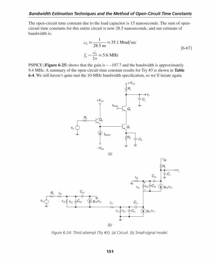
Bandwidth Estimation Techniques and the Method of Open-Circuit Time Constants
151
The open-circuit time constant due to the load capacitor is 15 nanoseconds. The sum of open-circuit time constants for this entire circuit is now 28.5 nanoseconds, and our estimate of bandwidth is:
135.1 Mrad sec
28.5 ns
5.6 MHz2
h
hhf
ω
ωπ
≈ ≈
= ≈
[6-67]
PSPICE (Figure 6-25) shows that the gain is ∼ –107.7 and the bandwidth is approximately 9.4 MHz. A summary of the open-circuit time constant results for Try #3 is shown in Table 6-4. We still haven’t quite met the 10-MHz bandwidth specifi cation, so we’ll iterate again.
(a)
vo
Rs
+–
CL
RL
+VCC
Q2
vBIAS
Q1
IBIAS3
CERE
–VEE
Q3
vin
+VCC
vin rπ3
rx3Rs
vπ3 Cπ3
gm1vπ1
Cμ3
gm3vπ3 rx1
rπ1 vπ1 Cπ1
Cμ1
rx2Cμ2
Cπ2vπ2rπ2
+
–gm2vπ2
CL
RL
+–
vo
(b)
Figure 6-24: Third attempt (Try #3). (a) Circuit. (b) Small-signal model.
Thompson Book.indb 151 3/20/2006 11:34:54 AM
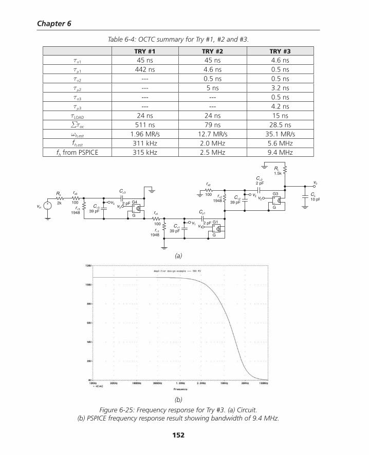
Chapter 6
152
Table 6-4: OCTC summary for Try #1, #2 and #3.
TRY #1 TRY #2 TRY #3τπ1 45 ns 45 ns 4.6 nsτμ1 442 ns 4.6 ns 0.5 nsτπ2 --- 0.5 ns 0.5 nsτμ2 --- 5 ns 3.2 nsτπ3 --- --- 0.5 nsτμ3 --- --- 4.2 ns
τLOAD 24 ns 24 ns 15 ns∑τoc 511 ns 79 ns 28.5 nsωh,est 1.96 MR/s 12.7 MR/s 35.1 MR/sfh,est 311 kHz 2.0 MHz 5.6 MHz
fh from PSPICE 315 kHz 2.5 MHz 9.4 MHz
(b)
Figure 6-25: Frequency response for Try #3. (a) Circuit. (b) PSPICE frequency response result showing bandwidth of 9.4 MHz.
(a)
vin rπ31948
rx3Rs
v3Cπ3
39 pF
Cμ3
rx1 Cμ1
rx2
+–
+–
2k 100v3
100 Cπ139 pFrπ1
1948
G4
G
2 pF
v1 v1 +–
+–
Cμ22 pF
G3
G1
G
G
Cπ239 pF
rπ21948
100 v2 v2
RL1.5k
v0
CL10 pF
2 pF
Thompson Book.indb 152 3/20/2006 11:34:54 AM
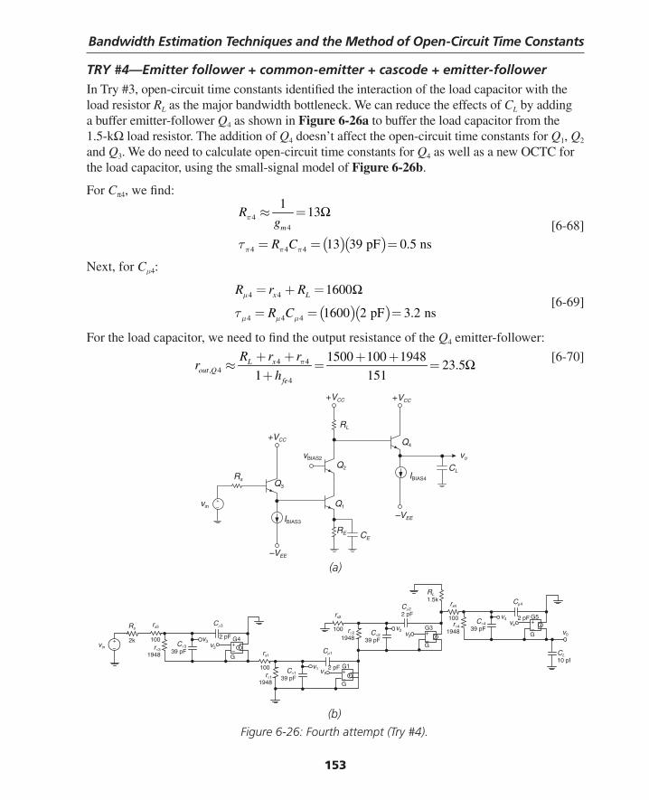
Bandwidth Estimation Techniques and the Method of Open-Circuit Time Constants
153
TRY #4—Emitter follower + common-emitter + cascode + emitter-followerIn Try #3, open-circuit time constants identifi ed the interaction of the load capacitor with the load resistor RL as the major bandwidth bottleneck. We can reduce the effects of CL by adding a buffer emitter-follower Q4 as shown in Figure 6-26a to buffer the load capacitor from the 1.5-kΩ load resistor. The addition of Q4 doesn’t affect the open-circuit time constants for Q1, Q2 and Q3. We do need to calculate open-circuit time constants for Q4 as well as a new OCTC for the load capacitor, using the small-signal model of Figure 6-26b.
For Cπ4, we fi nd:
( )( )
44
4 4 4
113
13 39 pF 0.5 nsm
Rg
R C
π
π π πτ
≈ =
= = =
Ω [6-68]
Next, for Cμ4:
( )( )
4 4
4 4 4
1600
1600 2 pF 3.2 ns
x LR r R
R C
μ
μ μ μτ
= + =
= = =
Ω [6-69]
For the load capacitor, we need to fi nd the output resistance of the Q4 emitter-follower:
4 4, 4
4
1500 100 194823.5
1 151L x
out Qfe
R r rr
hπ+ + + +
≈ = =+
Ω [6-70]
(b)
Figure 6-26: Fourth attempt (Try #4).
vo
Rs
+–
RL
+VCC
Q2
vBIAS2
Q1
IBIAS3
CERE
–VEE
Q3
vin
+VCC
–VEE
+VCC
IBIAS4
CL
Q4
vin rπ31948
rx3Rs
v3Cπ339 pF
Cμ3
rx1Cμ1
rx2
+–
+–
2k 100v3
100 Cπ139 pFrπ1
1948
G4
G
2 pF
v1 v1
+–
Cμ22 pF
G3
G1
G
G
Cπ239 pF
rπ21948
100 v2v2
RL1.5k
v0
CL10 pF
2 pF
G5
G
v4v4
Cμ4
2 pFCπ439 pF
rx4
100rπ4
1948
+–
+–
(a)
Thompson Book.indb 153 3/20/2006 11:34:55 AM
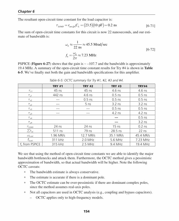
Chapter 6
154
The resultant open-circuit time constant for the load capacitor is:
( )( ), 4 23.5 10 pF 0.2 nsLOAD out Q Lr Cτ = = = [6-71]
The sum of open-circuit time constants for this circuit is now 22 nanoseconds, and our esti-mate of bandwidth is:
145.5 Mrad sec
22 ns
7.23 MHz2
h
hhf
ω
ωπ
≈ ≈
= ≈
[6-72]
PSPICE (Figure 6-27) shows that the gain is ∼ –107.7 and the bandwidth is approximately 19.4 MHz. A summary of the open-circuit time constant results for Try #4 is shown in Table 6-5. We’ve fi nally met both the gain and bandwidth specifi cations for this amplifi er.
Table 6-5: OCTC summary for Try #1, #2, #3 and #4.
TRY #1 TRY #2 TRY #3 TRY#4 τπ1 45 ns 45 ns 4.6 ns 4.6 nsτμ1 442 ns 4.6 ns 0.5 ns 0.5 nsτπ2 --- 0.5 ns 0.5 ns 0.5 nsτμ2 --- 5 ns 3.2 ns 3.2 nsτπ3 --- --- 0.5 ns 0.5 nsτμ3 --- --- 4.2 ns 4.2 nsτπ4 --- 0.5 nsτμ4 --- 3.2 ns
τLOAD 24 ns 24 ns 15 ns 0.2 ns∑τoc 511 ns 79 ns 28.5 ns 22 nsωh,est 1.96 MR/s 12.7 MR/s 35.1 MR/s 45.4 MR/sfh,est 311 kHz 2.0 MHz 5.6 MHz 7.23 MHz
fh from PSPICE 315 kHz 2.5 MHz 9.4 MHz 19.4 MHz
We see that using the method of open-circuit time constants we are able to identify the major bandwidth bottlenecks and attack them. Furthermore, the OCTC method gives a pessimistic approximation of bandwidth, so that actual bandwidth will be higher. Note the following OCTC caveats:
• The bandwidth estimate is always conservative.
• The estimate is accurate if there is a dominant pole.
• The OCTC estimate can be over-pessimistic if there are dominant complex poles, since the method assumes real-axis poles.
• Not all capacitors are used in OCTC analysis (e.g., coupling and bypass capacitors).
– OCTC applies only to high-frequency models.
Thompson Book.indb 154 3/20/2006 11:34:55 AM
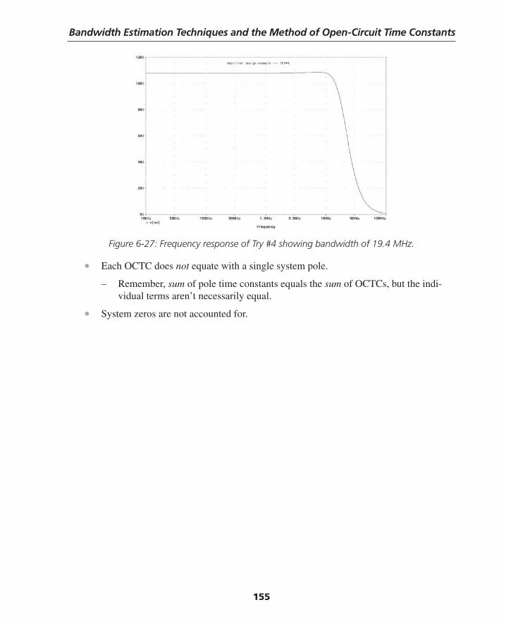
Bandwidth Estimation Techniques and the Method of Open-Circuit Time Constants
155
Figure 6-27: Frequency response of Try #4 showing bandwidth of 19.4 MHz.
• Each OCTC does not equate with a single system pole.
– Remember, sum of pole time constants equals the sum of OCTCs, but the indi-vidual terms aren’t necessarily equal.
• System zeros are not accounted for.
Thompson Book.indb 155 3/20/2006 11:34:56 AM
156
Chapter 6 Problems
Problem 6.1Using the method of open-circuit time constants, estimate the bandwidth (in Hz) of the RC ladder in Figure 6-28.
Figure 6-29: Circuit for Problem 6.2.
Problem 6.3The transistor amplifi er shown (Figure 6-30) is a high-bandwidth, common-emitter confi guration used to amplify a video signal. A small-signal video input drives from a 75Ω source impedance and is terminated with a 75Ω termination resistor. The transistor is biased with a DC power supply VDC = 5.7 volts. For the MPSH20 transistor you may assume rx = 20Ω, AC beta hfe ≈ DC beta hFE = 25, Cμ = 0.9 pF and fT = 630 MHz. Make reasonable approximations, state them, and justify them. Assume room temperature is 25ºC and hence kT/q = 26 millivolts.
R1
C4
10 pFR5
5
vi
+
vo
–
C3
10 pFC2
10 pFC1
10 pF
10
R2
10
R3
10
R4
10+–
R1
vi
+
vo
–
C1
1μFC2
1μF
10k
R2
10k+–
Figure 6-28: RC ladder for Problem 6.1.
Problem 6.2For the circuit in Figure 6-29:
(a) Estimate the –3dB bandwidth using the method of open-circuit time constants.
(b) Find the –3dB bandwidth exactly by calculation or by using SPICE.
Thompson Book.indb 156 3/20/2006 11:34:56 AM
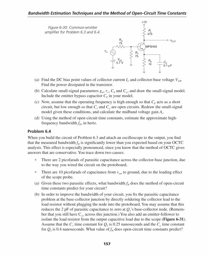
Bandwidth Estimation Techniques and the Method of Open-Circuit Time Constants
157
(a) Find the DC bias point values of collector current IC and collector-base voltage VCB. Find the power dissipated in the transistor.
(b) Calculate small-signal parameters gm, rπ, Cπ and Cμ, and draw the small-signal model. Include the emitter bypass capacitor CE in your model.
(c) Now, assume that the operating frequency is high enough so that CE acts as a short circuit, but low enough so that Cπ and Cμ are open circuits. Redraw the small-signal model given these conditions, and calculate the midband voltage gain Av.
(d) Using the method of open-circuit time constants, estimate the approximate high- frequency bandwidth fH, in hertz.
Problem 6.4When you build the circuit of Problem 6.3 and attach an oscilloscope to the output, you fi nd that the measured bandwidth fH is signifi cantly lower than you expected based on your OCTC analysis. This effect is especially pronounced, since you know that the method of OCTC gives answers that are conservative. You trace down two causes:
• There are 2 picofarads of parasitic capacitance across the collector-base junction, due to the way you wired the circuit on the protoboard;
• There are 10 picofarads of capacitance from vout to ground, due to the loading effect of the scope probe.
(a) Given these two parasitic effects, what bandwidth fH does the method of open-circuit time constants predict for your circuit?
(b) In order to improve the bandwidth of your circuit, you fi x the parasitic capacitance problem at the base-collector junction by directly soldering the collector lead to the load resistor without plugging the node into the protoboard. You may assume that this reduces the 2 pF of parasitic capacitance to zero at Q1’s base-collector node. (Remem-ber that you still have Cμ1 across this junction.) You also add an emitter-follower to isolate the load resistor from the output capacitive load due to the scope (Figure 6-31). Assume that the Cπ time constant for Q2 is 0.25 nanoseconds and the Cμ time constant for Q2 is 0.4 nanoseconds. What value of fH does open-circuit time constants predict?
MPSH20vin
vOUT
RL470
RE1k
+10
VDC5.7 V
RS75
CE0.1 μF
RT75
Figure 6-30: Common-emitter amplifi er for Problem 6.3 and 6.4.
Thompson Book.indb 157 3/20/2006 11:34:56 AM
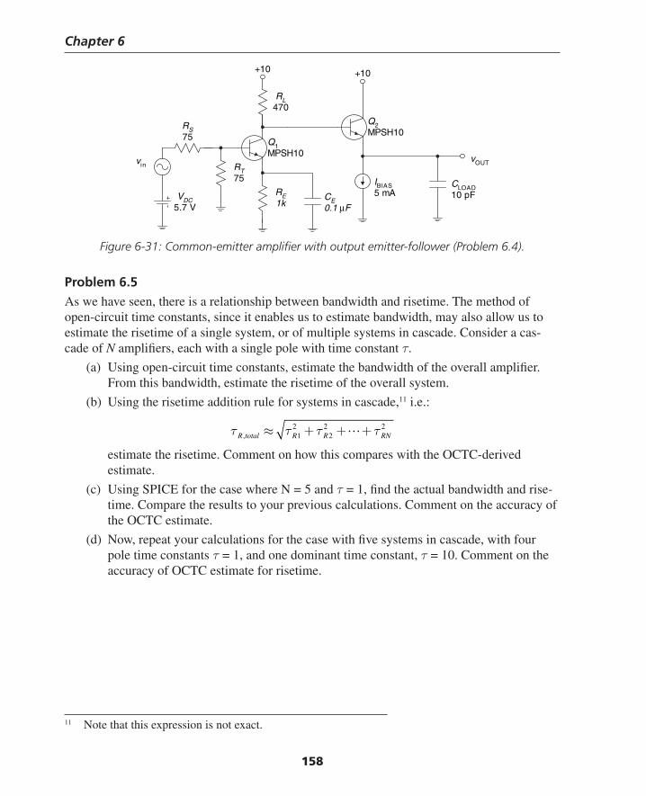
Chapter 6
158
Figure 6-31: Common-emitter amplifi er with output emitter-follower (Problem 6.4).
Problem 6.5As we have seen, there is a relationship between bandwidth and risetime. The method of open-circuit time constants, since it enables us to estimate bandwidth, may also allow us to estimate the risetime of a single system, or of multiple systems in cascade. Consider a cas-cade of N amplifi ers, each with a single pole with time constant τ.
(a) Using open-circuit time constants, estimate the bandwidth of the overall amplifi er. From this bandwidth, estimate the risetime of the overall system.
(b) Using the risetime addition rule for systems in cascade,11 i.e.:
2 2 2, 1 2R total R R RNτ τ τ τ≈ + + +
estimate the risetime. Comment on how this compares with the OCTC-derived estimate.
(c) Using SPICE for the case where N = 5 and τ = 1, fi nd the actual bandwidth and rise-time. Compare the results to your previous calculations. Comment on the accuracy of the OCTC estimate.
(d) Now, repeat your calculations for the case with fi ve systems in cascade, with four pole time constants τ = 1, and one dominant time constant, τ = 10. Comment on the accuracy of OCTC estimate for risetime.
Q1MPSH10
vinvOUT
RL470
RE1k
+10
VDC5.7 V
RS75
CE0.1 μF
Q2MPSH10
+10
IBIAS5 mA
CLOAD10 pF
RT75
11 Note that this expression is not exact.
Thompson Book.indb 158 3/20/2006 11:34:57 AM
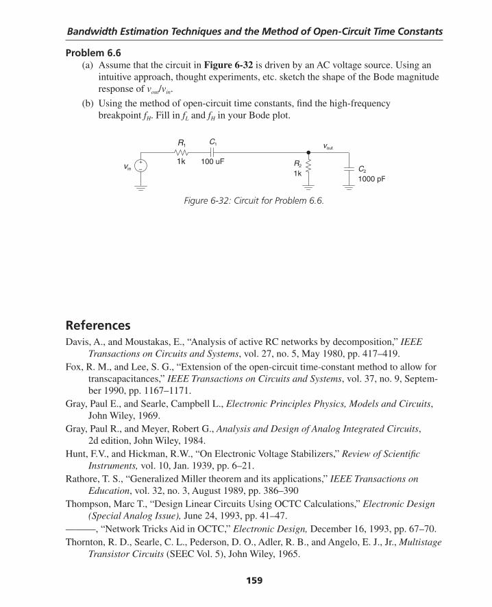
Bandwidth Estimation Techniques and the Method of Open-Circuit Time Constants
159
Problem 6.6(a) Assume that the circuit in Figure 6-32 is driven by an AC voltage source. Using an
intuitive approach, thought experiments, etc. sketch the shape of the Bode magnitude response of vout/vin.
(b) Using the method of open-circuit time constants, fi nd the high-frequency breakpoint fH. Fill in fL and fH in your Bode plot.
R1
vin C2
1000 pF
1k 100 uF
C1 vout
+–
R2
1k
Figure 6-32: Circuit for Problem 6.6.
ReferencesDavis, A., and Moustakas, E., “Analysis of active RC networks by decomposition,” IEEE
Transactions on Circuits and Systems, vol. 27, no. 5, May 1980, pp. 417–419.Fox, R. M., and Lee, S. G., “Extension of the open-circuit time-constant method to allow for
transcapacitances,” IEEE Transactions on Circuits and Systems, vol. 37, no. 9, Septem-ber 1990, pp. 1167–1171.
Gray, Paul E., and Searle, Campbell L., Electronic Principles Physics, Models and Circuits, John Wiley, 1969.
Gray, Paul R., and Meyer, Robert G., Analysis and Design of Analog Integrated Circuits, 2d edition, John Wiley, 1984.
Hunt, F.V., and Hickman, R.W., “On Electronic Voltage Stabilizers,” Review of Scientifi c Instruments, vol. 10, Jan. 1939, pp. 6–21.
Rathore, T. S., “Generalized Miller theorem and its applications,” IEEE Transactions on Education, vol. 32, no. 3, August 1989, pp. 386–390
Thompson, Marc T., “Design Linear Circuits Using OCTC Calculations,” Electronic Design (Special Analog Issue), June 24, 1993, pp. 41–47.
———, “Network Tricks Aid in OCTC,” Electronic Design, December 16, 1993, pp. 67–70.Thornton, R. D., Searle, C. L., Pederson, D. O., Adler, R. B., and Angelo, E. J., Jr., Multistage
Transistor Circuits (SEEC Vol. 5), John Wiley, 1965.
Thompson Book.indb 159 3/20/2006 11:34:57 AM

Thompson Book.indb 160 3/20/2006 11:34:57 AM
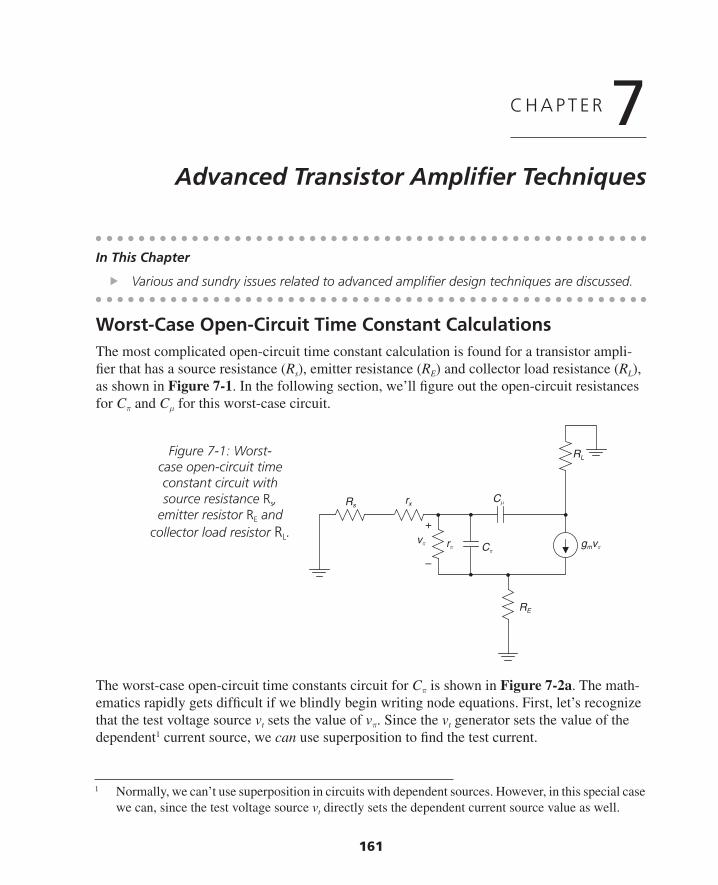
161
C H A P T E R 7Advanced Transistor Amplifi er Techniques
Worst-Case Open-Circuit Time Constant CalculationsThe most complicated open-circuit time constant calculation is found for a transistor ampli-fi er that has a source resistance (Rs), emitter resistance (RE) and collector load resistance (RL), as shown in Figure 7-1. In the following section, we’ll fi gure out the open-circuit resistances for Cπ and Cμ for this worst-case circuit.
In This Chapter
Various and sundry issues related to advanced amplifi er design techniques are discussed.
Figure 7-1: Worst-case open-circuit time constant circuit with source resistance Rs,
emitter resistor RE and collector load resistor RL.
Rsrx
Cμ
RL
RE
Cπ
vπ gmvπrπ
+
–
The worst-case open-circuit time constants circuit for Cπ is shown in Figure 7-2a. The math-ematics rapidly gets diffi cult if we blindly begin writing node equations. First, let’s recognize that the test voltage source vt sets the value of vπ. Since the vt generator sets the value of the dependent1 current source, we can use superposition to fi nd the test current.
1 Normally, we can’t use superposition in circuits with dependent sources. However, in this special case we can, since the test voltage source vt directly sets the dependent current source value as well.
Thompson Book.indb 161 3/20/2006 11:34:57 AM
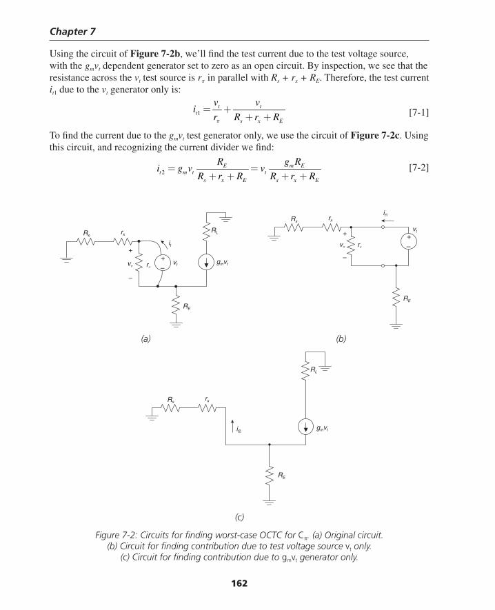
Chapter 7
162
Rsrx
RL
RE
vπgmvtrπ
+
–
Rsrx
RL
RE
gmvtit2
Rsrx
it1
RE
vπ rπ
+
–
+–
vt
vt
it
+–
Using the circuit of Figure 7-2b, we’ll fi nd the test current due to the test voltage source, with the gmvt dependent generator set to zero as an open circuit. By inspection, we see that the resistance across the vt test source is rπ in parallel with Rs + rx + RE. Therefore, the test current it1 due to the vt generator only is:
1t t
ts x E
v vi
r R r Rπ
= ++ + [7-1]
To fi nd the current due to the gmvt test generator only, we use the circuit of Figure 7-2c. Using this circuit, and recognizing the current divider we fi nd:
2
m EEt m t t
s x E s x E
g RRi g v v
R r R R r R= =
+ + + + [7-2]
(a) (b)
(c)
Figure 7-2: Circuits for fi nding worst-case OCTC for Cπ. (a) Original circuit. (b) Circuit for fi nding contribution due to test voltage source vt only.
(c) Circuit for fi nding contribution due to gmvt generator only.
Thompson Book.indb 162 3/20/2006 11:34:58 AM
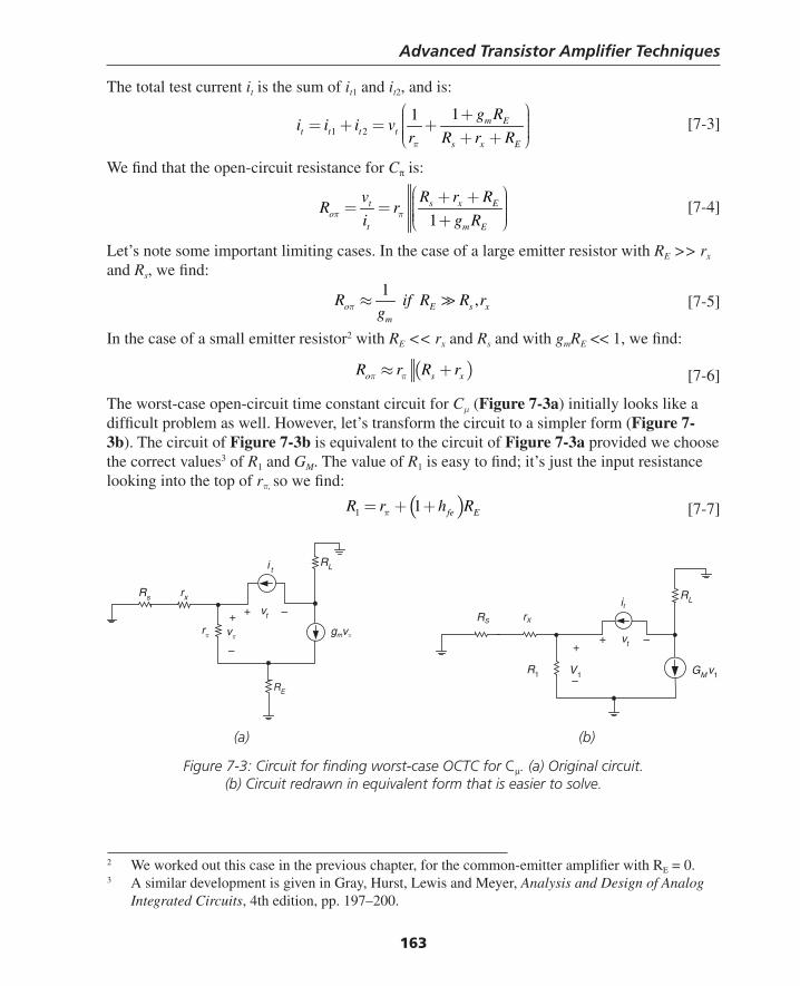
Advanced Transistor Amplifi er Techniques
163
The total test current it is the sum of it1 and it2, and is:
1 2
11 m Et t t t
s x E
g Ri i i v
r R r Rπ
⎛ ⎞+ ⎟⎜ ⎟= + = +⎜ ⎟⎜ ⎟⎜ + +⎝ ⎠ [7-3]
We fi nd that the open-circuit resistance for Cπ is:
1
t s x Eo
t m E
v R r RR r
i g Rπ π
⎛ ⎞+ + ⎟⎜ ⎟= = ⎜ ⎟⎜ ⎟⎜ +⎝ ⎠ [7-4]
Let’s note some important limiting cases. In the case of a large emitter resistor with RE >> rx and Rs, we fi nd:
1
,o E s xm
R if R R rgπ ≈ [7-5]
In the case of a small emitter resistor2 with RE << rx and Rs and with gmRE << 1, we fi nd:
( )o s xR r R rπ π≈ + [7-6]
The worst-case open-circuit time constant circuit for Cμ (Figure 7-3a) initially looks like a diffi cult problem as well. However, let’s transform the circuit to a simpler form (Figure 7-3b). The circuit of Figure 7-3b is equivalent to the circuit of Figure 7-3a provided we choose the correct values3 of R1 and GM. The value of R1 is easy to fi nd; it’s just the input resistance looking into the top of rπ, so we fi nd:
( )1 1 fe ER r h Rπ= + + [7-7]
2 We worked out this case in the previous chapter, for the common-emitter amplifi er with RE = 0.3 A similar development is given in Gray, Hurst, Lewis and Meyer, Analysis and Design of Analog
Integrated Circuits, 4th edition, pp. 197–200.
RL
rxRs
RE
i t
+
–
rπ vπ gmvπ
+
–
rX
GM v1
RL
RS
R1
it
V1
+ –vt
+ –vt
(a) (b)
Figure 7-3: Circuit for fi nding worst-case OCTC for Cμ. (a) Original circuit. (b) Circuit redrawn in equivalent form that is easier to solve.
Thompson Book.indb 163 3/20/2006 11:34:58 AM
Chapter 7
164
Next, we need to fi nd the value of the new dependent generator. We can make use of the fact that the output currents from the old and transformed circuits are the same, or:
1m Mg v G vπ = [7-8]
Let’s imagine using a test current source it to solve for vπ in Figure 7-3a, and for v1 in Figure 7-3b. We fi nd4 for vπ:
( )1
s xt
s x fe E
R rv i r
R r r h Rπ π
π
⎛ ⎞⎟+⎜ ⎟⎜= ⎟⎜ ⎟⎜ ⎟+ + + + ⎟⎜⎝ ⎠ [7-9]
Next, we solve for v1:
( ) ( ) ( )( )
( )1
11
1
1
s x fe Es xt
s x s x fe E
R r r h RR r Rv i
R r R R r r h R
π
π
⎛ ⎞ + + ++ ⎟⎜ ⎟⎜= =⎟⎜ ⎟⎟⎜ + + + + + +⎝ ⎠ [7-10]
Next, we solve5 for GM:
( )( )
( ) ( )( )( )
1
1
11 1
1
s x
s x fe Em m mM m
E m Es x fe E m E
s x fe E
R rr
R r r h Rg v g gG g
Rv g RR r r h R g Rr
R r r h R
πππ
π
ππ
⎛ ⎞+ ⎟⎜ ⎟⎜ ⎟⎜ ⎟⎜ ⎟+ + + + ⎟⎜⎝ ⎠= = = ≈
⎛ ⎞ ++ + + ⎟⎜ + +⎟⎜ ⎟⎜ ⎟⎜ ⎟+ + + +⎜ ⎟⎟⎜⎝ ⎠
[7-11]
To summarize, the worst-case open-circuit resistance for Cμ is:
( ) ( ) ( )( )1 1
1 1 1
1
o EQ L M EQ L
EQ s x s x fe E
mM
m E
R R R G R R
R R r R R r r h R
gG
g R
μ
π
= + +
= + = + + +
≈+
[7-12]
4 This is done by calculating a current divider. The fraction of the it current that travels through rπ is:
( )1
s x
s x fe E
R r
R r r h Rπ
⎛ ⎞⎟+⎜ ⎟⎜ ⎟⎜ ⎟⎜ ⎟+ + + + ⎟⎜⎝ ⎠5 Yes, I know it’s a mess, but follow it through. It arrives at a nice simple result. Note that gm >> 1/rπ.
Thompson Book.indb 164 3/20/2006 11:34:59 AM
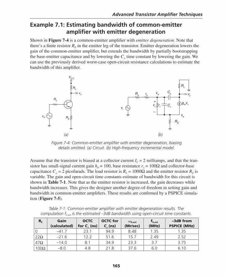
Advanced Transistor Amplifi er Techniques
165
Example 7.1: Estimating bandwidth of common-emitter amplifi er with emitter degenerationShown in Figure 7-4 is a common-emitter amplifi er with emitter degeneration. Note that there’s a fi nite resistor RE in the emitter leg of the transistor. Emitter degeneration lowers the gain of the common-emitter amplifi er, but extends the bandwidth by partially bootstrapping the base-emitter capacitance and by lowering the Cμ time constant by lowering the gain. We can use the previously derived worst-case open-circuit resistance calculations to estimate the bandwidth of this amplifi er.
(a) (b)
Figure 7-4: Common-emitter amplifi er with emitter degeneration, biasing details omitted. (a) Circuit. (b) High-frequency incremental model.
vo
VCC
RE
RL
vin
Rs +
–
rx
rπ Cπ
Cμ
gmvπvπ
vova
RL
Rs
vi
RE
ve
Assume that the transistor is biased at a collector current IC = 2 milliamps, and that the tran-sistor has small-signal current gain hfe = 100, base resistance rx = 100Ω and collector-base capacitance Cμ = 2 picofarads. The load resistor is RL = 1000Ω and the emitter resistor RE is variable. The gain and open-circuit time constants estimate of bandwidth for this circuit is shown in Table 7-1. Note that as the emitter resistor is increased, the gain decreases while bandwidth increases. This gives the designer another degree-of-freedom in setting gain and bandwidth in common-emitter amplifi ers. These results are confi rmed by a PSPICE simula-tion (Figure 7-5).
Table 7-1: Common-emitter amplifi er with emitter degeneration results. The computation fh,est is the estimated –3dB bandwidth using open-circuit time constants.
RE Gain (calculated)
OCTC for Cπ (ns)
OCTC for Cμ (ns)
ωh,est
(Mr/sec)fh,est
(MHz)–3dB from
PSPICE (MHz)0 –41.7 23.1 94.9 8.48 1.35 1.35 22Ω –21.6 12.2 51.6 15.7 2.49 2.52 47Ω –14.0 8.1 34.9 23.3 3.7 3.75100Ω –8.0 4.8 21.8 37.6 6.0 6.10
Thompson Book.indb 165 3/20/2006 11:35:00 AM
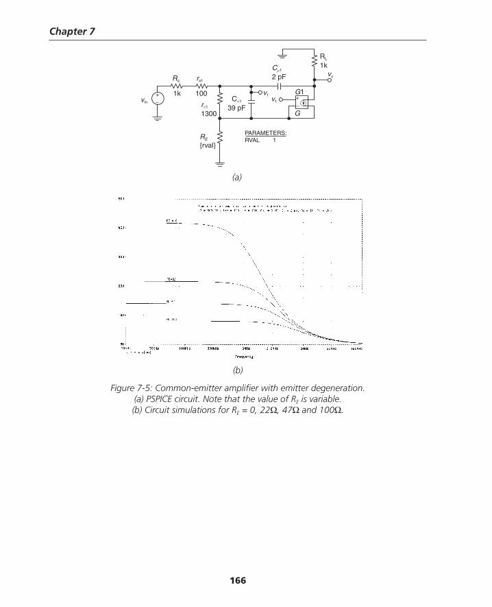
Chapter 7
166
(a)
+–vin
rx1Rs
Cμ1
2 pF
RL
1kvo
G
G1v1v1Cπ1
39 pFrπ1
1300
1001k+
–
RE
{rval}
PARAMETERS:RVAL 1
(b)
Figure 7-5: Common-emitter amplifi er with emitter degeneration. (a) PSPICE circuit. Note that the value of RE is variable. (b) Circuit simulations for RE = 0, 22Ω, 47Ω and 100Ω.
Thompson Book.indb 166 3/20/2006 11:35:00 AM
Advanced Transistor Amplifi er Techniques
167
Example 7.2: Gain of differential amplifi er with emitter degenerationThe model of the common-emitter amplifi er with emitter degeneration can be used to analyze the gain of the differential amplifi er with emitter degeneration (Figure 7-6a) when operated in the differential mode. By half-circuit techniques, we see that in the differential mode,6 the circuit is equivalent to the common-emitter amplifi er with emitter degeneration (Figure 7-6b). Inclusion of emitter resistors RE increases the range of differential input voltages over which the differential amplifi er provides approximately linear gain.7
Shown in Figure 7-7 is a PSPICE simulation of a differential amplifi er with emitter degenera-tion. The base of transistor Q2 is grounded and the voltage at the base of transistor Q1 is swept from –500 millivolts to +500 millivolts, and the voltage at the base of Q2 is swept simultane-ously from +500 millivolts to –500 millivolts. Results are shown in the simulation of Figure 7-7b. With RE = 0, the amplifi er is a standard differential amplifi er, and the output swings over its full range when the input varies a few kT/q. With RE = 100Ω and 220Ω, the amplifi er has linear gain over a much wider input voltage range.
(a) (b)
Figure 7-6: Differential amplifi er with emitter degeneration. (a) Circuit. (b) Low-frequency small-signal model for the differential mode of operation.
RE
vπ gmvπrπ
+
–
vid
R
R R
+V
–V
V2V1RE RE
IBIAS
2
vod
2+–
6 In the differential mode, the input to one of the transistors is vid/2 and the output of one of the transistors is vod/2.
7 However, there are tradeoffs—an increase in noise due to the resistors, as well as a lowering of
differential gain and CMRR. A full discussion is given in Grebene’s Bipolar and MOS Analog Integrated Circuit Design, pp. 221–224.
Thompson Book.indb 167 3/20/2006 11:35:01 AM
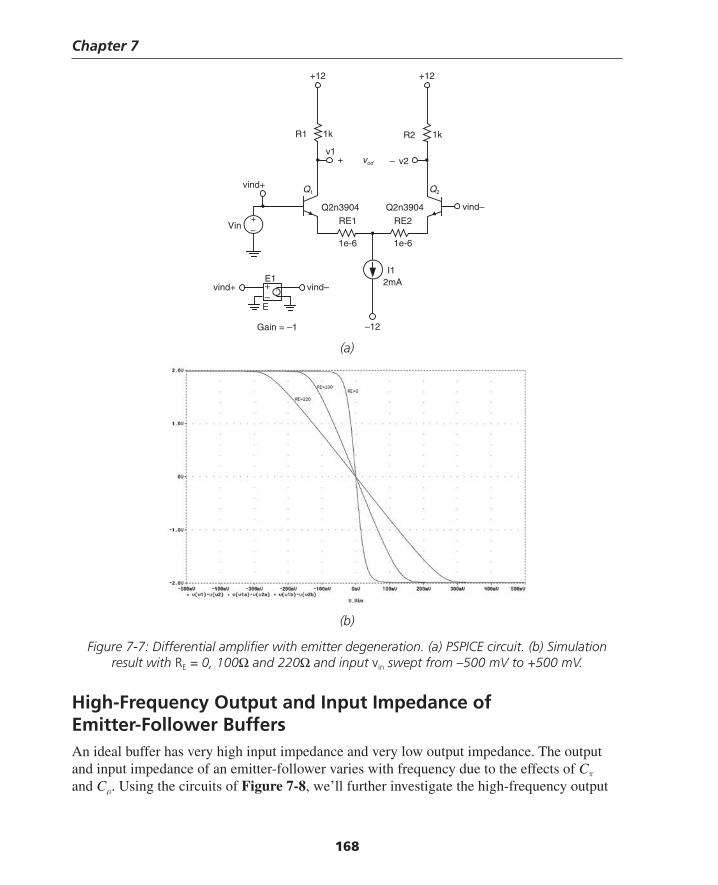
Chapter 7
168
(b)
Figure 7-7: Differential amplifi er with emitter degeneration. (a) PSPICE circuit. (b) Simulation result with RE = 0, 100Ω and 220Ω and input vin swept from –500 mV to +500 mV.
(a)
+–
E1vind+ vind–
E
Gain = –1
+–
+–
vind–
vind+
RE1 RE2
+12 +12
R1 R2
Q1 Q2
v1v2
1k 1k
1e-6 1e-6
Vin
I12mA
–12
Q2n3904 Q2n3904
+ –vod
High-Frequency Output and Input Impedance of Emitter-Follower BuffersAn ideal buffer has very high input impedance and very low output impedance. The output and input impedance of an emitter-follower varies with frequency due to the effects of Cπ and Cμ. Using the circuits of Figure 7-8, we’ll further investigate the high-frequency output
Thompson Book.indb 168 3/20/2006 11:35:02 AM
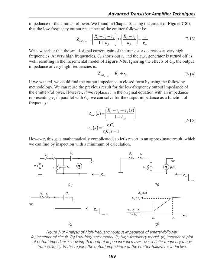
Advanced Transistor Amplifi er Techniques
169
impedance of the emitter-follower. We found in Chapter 5, using the circuit of Figure 7-8b, that the low-frequency output resistance of the emitter-follower is:
0
1
1s x s x
outfe fe m
R r r R rZ
h h gω
π→
⎛ ⎞ ⎛ ⎞+ + +⎟ ⎟⎜ ⎜⎟ ⎟⎜ ⎜= ≈ +⎟ ⎟⎜ ⎜⎟ ⎟⎜ ⎜⎟ ⎟+⎝ ⎠ ⎝ ⎠ [7-13]
We saw earlier that the small-signal current gain of the transistor decreases at very high frequencies. At very high frequencies, Cπ shorts out rπ and the gmvπ generator is turned off as well, resulting in the incremental model of Figure 7-8c. Ignoring the effects of Cμ, the output impedance at very high frequencies is:
out s xZ R rω→∞
= + [7-14]
If we wanted, we could fi nd the output impedance in closed form by using the following methodology. We can reuse the previous result for the low-frequency output impedance of the emitter-follower. However, if we replace rπ in the original equation with an impedance representing rπ in parallel with Cπ, we can solve for the output impedance as a function of frequency:
( )( )
( )
1
1
s xout
fe
R r z sZ s
h
r Cz s
r C s
π
π ππ
π π
⎛ ⎞+ + ⎟⎜ ⎟⎜= ⎟⎜ ⎟⎜ ⎟+⎝ ⎠
=+
[7-15]
However, this gets mathematically complicated, so let’s resort to an approximate result, which we can fi nd by inspection with a minimum of calculation.
Cπvπ
+
–
rxRs
Cμ
rπ
Zout
+–
Zout
ω→∞
CμrxRs
rxRs
Zout
ω→0
gmvπvπ
+
–rπ
outZ (ω)
Rs + rx
Rs + rx + rπ
1 + hfe
ω1 ω2
ω
vi
(a) (b)
(c) (d)
Figure 7-8: Analysis of high-frequency output impedance of emitter-follower. (a) Incremental circuit. (b) Low-frequency model. (c) High-frequency model. (d) Impedance plot of output impedance showing that output impedance increases over a fi nite frequency range
from ω1 to ω2. In this region, the output impedance of the emitter-follower is inductive.
Thompson Book.indb 169 3/20/2006 11:35:02 AM
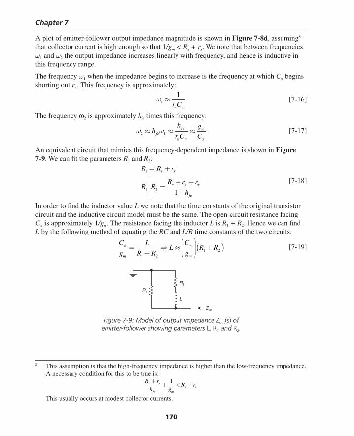
Chapter 7
170
A plot of emitter-follower output impedance magnitude is shown in Figure 7-8d, assuming8 that collector current is high enough so that 1/gm < Rs + rx. We note that between frequencies ω1 and ω2 the output impedance increases linearly with frequency, and hence is inductive in this frequency range.
The frequency ω1 when the impedance begins to increase is the frequency at which Cπ begins shorting out rπ. This frequency is approximately:
1
1
r Cπ π
ω ≈ [7-16]
The frequency ω2 is approximately hfe times this frequency:
2 1fe m
fe
h gh
r C Cπ π π
ω ω≈ ≈ ≈ [7-17]
An equivalent circuit that mimics this frequency-dependent impedance is shown in Figure 7-9. We can fi t the parameters R1 and R2:
1
1 2 1
s x
s x
fe
R R r
R r rR R
hπ
= +
+ +=
+
[7-18]
In order to fi nd the inductor value L we note that the time constants of the original transistor circuit and the inductive circuit model must be the same. The open-circuit resistance facing Cπ is approximately 1/gm. The resistance facing the inductor L is R1 + R2. Hence we can fi nd L by the following method of equating the RC and L/R time constants of the two circuits:
( )1 21 2m m
C CLL R R
g R R gπ π
⎛ ⎞⎟⎜ ⎟= ⇒ ≈ +⎜ ⎟⎜ ⎟⎜+ ⎝ ⎠ [7-19]
8 This assumption is that the high-frequency impedance is higher than the low-frequency impedance. A necessary condition for this to be true is:
1s xs x
fe m
R rR r
h g
++ < +
This usually occurs at modest collector currents.
R1
Zout
R2
L
Figure 7-9: Model of output impedance Zout(s) of emitter-follower showing parameters L, R1 and R2.
Thompson Book.indb 170 3/20/2006 11:35:03 AM
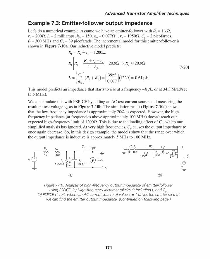
Advanced Transistor Amplifi er Techniques
171
Example 7.3: Emitter-follower output impedanceLet’s do a numerical example. Assume we have an emitter-follower with Rs = 1 kΩ, rx = 200Ω, Ic = 2 milliamps, hfe = 150, gm = 0.077Ω–1, rπ = 1950Ω, Cμ = 2 picofarads, fT = 300 MHz and Cπ = 39 picofarads. The incremental model for this emitter-follower is shown in Figure 7-10a. Our inductive model predicts:
( ) ( )
1
1 2 2
1 2
1200
20.9 20.91
39pf1220 0.61 H
0.077
s x
s x
fe
m
R R r
R r rR R R
h
CL R R
g
π
π
= + =
+ += = ⇒ ≈
+
⎛ ⎞ ⎛ ⎞⎟⎜ ⎟⎜⎟≈ + = ≈ μ⎜ ⎟⎜⎟ ⎟⎜ ⎜⎟⎜ ⎝ ⎠⎝ ⎠
Ω
Ω Ω [7-20]
This model predicts an impedance that starts to rise at a frequency ∼R2/L, or at 34.3 Mrad/sec (5.5 MHz).
We can simulate this with PSPICE by adding an AC test current source and measuring the resultant test voltage vt, as in Figure 7-10b. The simulation result (Figure 7-10c) shows that the low-frequency impedance is approximately 20Ω as expected. However, the high- frequency impedance (at frequencies above approximately 100 MHz) doesn't reach our expected high-frequency limit of 1200Ω. This is due to the loading effect of Cμ, which our simplifi ed analysis has ignored. At very high frequencies, Cμ causes the output impedance to once again decrease. So, in this design example, the models show that the range over which the output impedance is inductive is approximately 5 MHz to 100 MHz.
(a) (b)
Figure 7-10: Analysis of high-frequency output impedance of emitter-follower using PSPICE. (a) High-frequency incremental circuit including rx and Cμ.
(b) PSPICE circuit, where an AC current source of value it = 1 drives the emitter so that we can fi nd the emitter output impedance. (Continued on following page.)
Cπ
rx1RsCμ
rπ
+–
vi
1k 200
1950Ω
2 pF
39 pF
gmvπ
vo
rπ1950
rxRs
vacπ39 pF
cμ
vt
+–
2k 100
G
va 2 pF
G1
it
+vπ
–
Thompson Book.indb 171 3/20/2006 11:35:03 AM
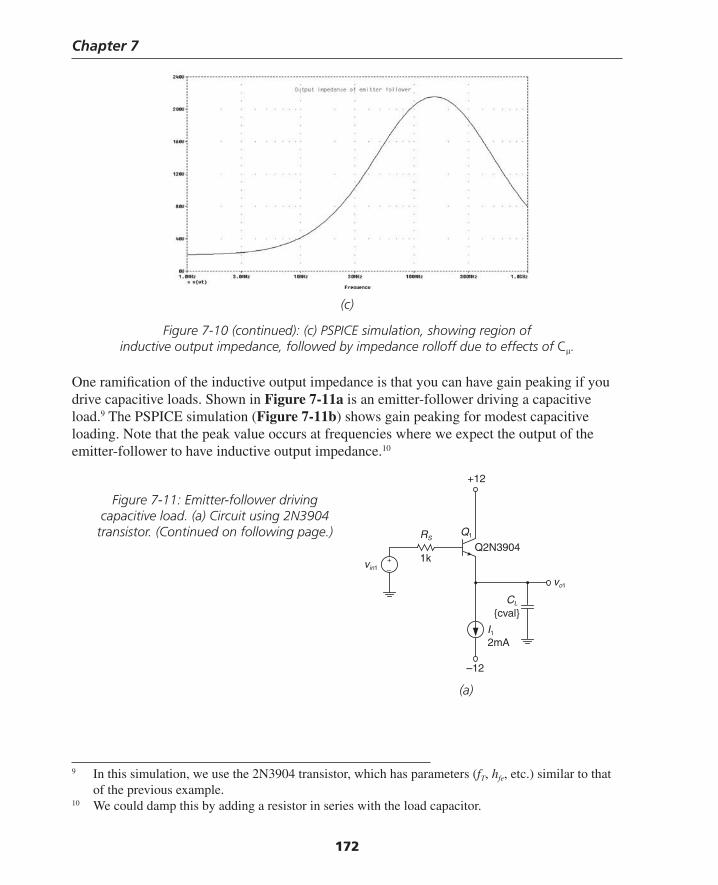
Chapter 7
172
(c)
Figure 7-10 (continued): (c) PSPICE simulation, showing region of inductive output impedance, followed by impedance rolloff due to effects of Cμ.
One ramifi cation of the inductive output impedance is that you can have gain peaking if you drive capacitive loads. Shown in Figure 7-11a is an emitter-follower driving a capacitive load.9 The PSPICE simulation (Figure 7-11b) shows gain peaking for modest capacitive loading. Note that the peak value occurs at frequencies where we expect the output of the emitter-follower to have inductive output impedance.10
9 In this simulation, we use the 2N3904 transistor, which has parameters (fT, hfe, etc.) similar to that of the previous example.
10 We could damp this by adding a resistor in series with the load capacitor.
+–
{cval}
+12
vo1
CL
I1
2mA
–12
Q2N3904
Q1RS
1kvin1
(a)
Figure 7-11: Emitter-follower driving capacitive load. (a) Circuit using 2N3904
transistor. (Continued on following page.)
Thompson Book.indb 172 3/20/2006 11:35:04 AM
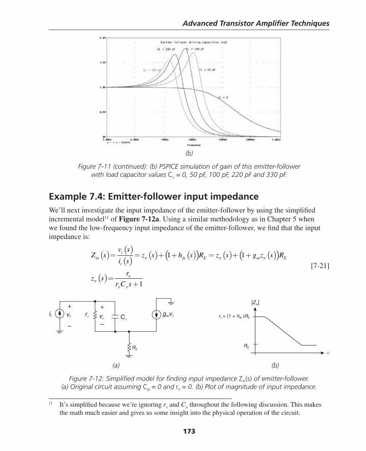
Advanced Transistor Amplifi er Techniques
173
(b)
Figure 7-11 (continued): (b) PSPICE simulation of gain of this emitter-follower with load capacitor values CL = 0, 50 pF, 100 pF, 220 pF and 330 pF.
Example 7.4: Emitter-follower input impedanceWe’ll next investigate the input impedance of the emitter-follower by using the simplifi ed incremental model11 of Figure 7-12a. Using a similar methodology as in Chapter 5 when we found the low-frequency input impedance of the emitter-follower, we fi nd that the input impedance is:
( )
( )( )
( ) ( )( ) ( ) ( )( )
( )
1 1
1
tin fe E m E
t
v sZ s z s h s R z s g z s R
i s
rz s
r C s
π π π
ππ
π π
= = + + = + +
=+
[7-21]
(a) (b)
Figure 7-12: Simplifi ed model for fi nding input impedance Zin(s) of emitter-follower. (a) Original circuit assuming Cμ = 0 and rx = 0. (b) Plot of magnitude of input impedance.
Cπvπ
+
–
it
RE
rπ gmvπ
RE
rπ + (1 + hfe )RE
ω
inZ+
–
vt
11 It’s simplifi ed because we’re ignoring rx and Cμ throughout the following discussion. This makes the math much easier and gives us some insight into the physical operation of the circuit.
Thompson Book.indb 173 3/20/2006 11:35:04 AM
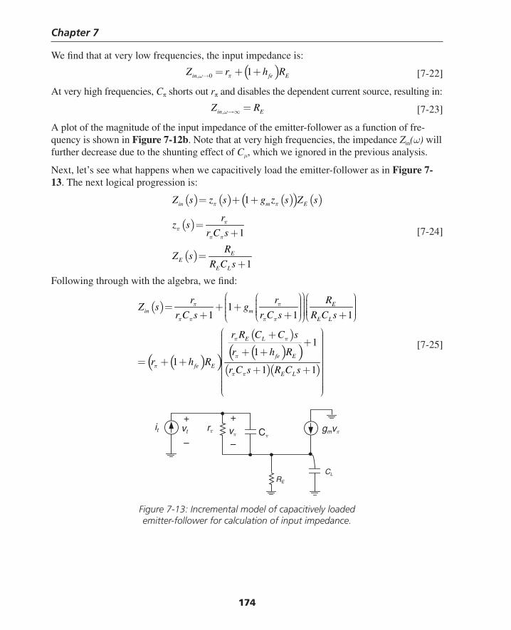
Chapter 7
174
We fi nd that at very low frequencies, the input impedance is:
( ), 0 1in fe EZ r h Rω π→ = + + [7-22]
At very high frequencies, Cπ shorts out rπ and disables the dependent current source, resulting in:
,in EZ Rω→∞ = [7-23]
A plot of the magnitude of the input impedance of the emitter-follower as a function of fre-quency is shown in Figure 7-12b. Note that at very high frequencies, the impedance Zin(ω) will further decrease due to the shunting effect of Cμ, which we ignored in the previous analysis.
Next, let’s see what happens when we capacitively load the emitter-follower as in Figure 7-13. The next logical progression is:
( ) ( ) ( )( ) ( )
( )
( )
1
1
1
in m E
EE
E L
Z s z s g z s Z s
rz s
r C s
RZ s
R C s
π π
ππ
π π
= + +
=+
=+
[7-24]
Following through with the algebra, we fi nd:
( )
( )( )
( )( )( )
( )( )
11 1 1
11
11 1
Ein m
E L
E L
fe E
fe EE L
r r RZ s g
r C s r C s R C s
r R C C s
r h Rr h R
r C s R C s
π π
π π π π
π π
π
ππ π
⎛ ⎞⎛ ⎞ ⎛ ⎞⎟⎜ ⎟ ⎟⎜ ⎜⎟⎟ ⎟⎜= + + ⎜ ⎜⎟⎟ ⎟⎜ ⎜ ⎜⎟ ⎟⎟ ⎜⎜ ⎟⎜+ + +⎝ ⎠⎝ ⎠⎝ ⎠⎛ ⎞+ ⎟⎜ ⎟+⎜ ⎟⎜ ⎟⎜ + + ⎟⎜ ⎟⎜ ⎟= + + ⎟⎜ ⎟⎜ + + ⎟⎜ ⎟⎜ ⎟⎜ ⎟⎜ ⎟⎟⎜⎝ ⎠
[7-25]
Cπvπ
+
–
it
RE
rπ gmvπ
+
–
vt
CL
Figure 7-13: Incremental model of capacitively loaded emitter-follower for calculation of input impedance.
Thompson Book.indb 174 3/20/2006 11:35:05 AM
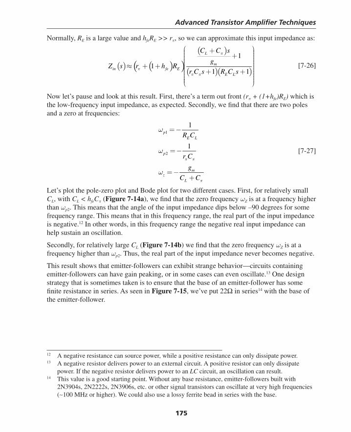
Advanced Transistor Amplifi er Techniques
175
Normally, RE is a large value and hfeRE >> rπ, so we can approximate this input impedance as:
( ) ( )( )( )
( )( )
1
11 1
L
min fe E
E L
C C s
gZ s r h R
r C s R C s
π
ππ π
⎛ ⎞+ ⎟⎜ ⎟+⎜ ⎟⎜ ⎟⎜ ⎟⎜ ⎟≈ + + ⎜ ⎟⎟⎜ + + ⎟⎜ ⎟⎜ ⎟⎜ ⎟⎜⎝ ⎠
[7-26]
Now let’s pause and look at this result. First, there’s a term out front (rπ + (1+hfe)RE) which is the low-frequency input impedance, as expected. Secondly, we fi nd that there are two poles and a zero at frequencies:
1
2
1
1
pE L
p
mz
L
R C
r C
g
C C
π π
π
ω
ω
ω
= −
= −
= −+
[7-27]
Let’s plot the pole-zero plot and Bode plot for two different cases. First, for relatively small CL, with CL < hfeCπ (Figure 7-14a), we fi nd that the zero frequency ωZ is at a frequency higher than ωp2. This means that the angle of the input impedance dips below –90 degrees for some frequency range. This means that in this frequency range, the real part of the input impedance is negative.12 In other words, in this frequency range the negative real input impedance can help sustain an oscillation.
Secondly, for relatively large CL (Figure 7-14b) we fi nd that the zero frequency ωZ is at a frequency higher than ωp2. Thus, the real part of the input impedance never becomes negative.
This result shows that emitter-followers can exhibit strange behavior—circuits containing emitter-followers can have gain peaking, or in some cases can even oscillate.13 One design strategy that is sometimes taken is to ensure that the base of an emitter-follower has some fi nite resistance in series. As seen in Figure 7-15, we’ve put 22Ω in series14 with the base of the emitter-follower.
12 A negative resistance can source power, while a positive resistance can only dissipate power.13 A negative resistor delivers power to an external circuit. A positive resistor can only dissipate
power. If the negative resistor delivers power to an LC circuit, an oscillation can result. 14 This value is a good starting point. Without any base resistance, emitter-followers built with
2N3904s, 2N2222s, 2N3906s, etc. or other signal transistors can oscillate at very high frequencies (∼100 MHz or higher). We could also use a lossy ferrite bead in series with the base.
Thompson Book.indb 175 3/20/2006 11:35:06 AM
Chapter 7
176
(a) (b)
Figure 7-14: Input impedance of capacitively loaded emitter-follower. (a) Result for relatively small CL, with CL < hfeCπ . (b) Result for relatively large CL with CL > hfeCπ.
σ
ωj
xxo–ωz –ωp2 –ωp1
σ
ωj
xox –ωp2 –ωz –ωp1
inZinZ
ωp1 ωz ωp2
log(ω) ωp1 ωp2 ωz
log(ω)
–20dB/dec
–40dB/dec
–20dB/dec
ωp1 ωp2 ωz
0
–45
–90
–135
–180
inZ�
log(ω) ωp1 ωz ωp2
0
–45
–90
–180
inZ�
log(ω)
+–
+12
CL
2N3904RB
22vin
RE
vo
–12
Figure 7-15: Resistor RB added to base of emitter-follower to reduce chances of oscillation.
Thompson Book.indb 176 3/20/2006 11:35:06 AM
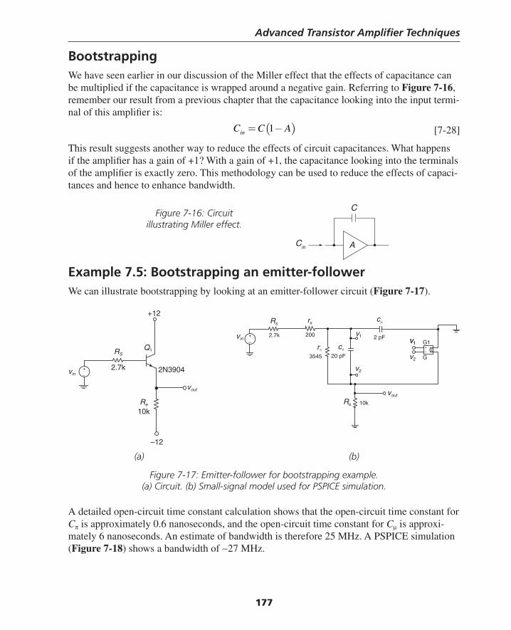
Advanced Transistor Amplifi er Techniques
177
BootstrappingWe have seen earlier in our discussion of the Miller effect that the effects of capacitance can be multiplied if the capacitance is wrapped around a negative gain. Referring to Figure 7-16, remember our result from a previous chapter that the capacitance looking into the input termi-nal of this amplifi er is:
( )1inC C A= − [7-28]
This result suggests another way to reduce the effects of circuit capacitances. What happens if the amplifi er has a gain of +1? With a gain of +1, the capacitance looking into the terminals of the amplifi er is exactly zero. This methodology can be used to reduce the effects of capaci-tances and hence to enhance bandwidth.
Example 7.5: Bootstrapping an emitter-followerWe can illustrate bootstrapping by looking at an emitter-follower circuit (Figure 7-17).
A
C
Cin
Figure 7-16: Circuit illustrating Miller effect.
(a) (b)
Figure 7-17: Emitter-follower for bootstrapping example. (a) Circuit. (b) Small-signal model used for PSPICE simulation.
A detailed open-circuit time constant calculation shows that the open-circuit time constant for Cπ is approximately 0.6 nanoseconds, and the open-circuit time constant for Cμ is approxi-mately 6 nanoseconds. An estimate of bandwidth is therefore 25 MHz. A PSPICE simulation (Figure 7-18) shows a bandwidth of ∼27 MHz.
+–
+12
2N3904
RS
2.7kvin
Re
10k
vout
–12
Q1
rxRs
vout
cμ
v1+–
2.7k 200
G
2 pFG1
+–
v2
v1v1
v2
Re 10k
cπ
20 pF
rπ
3545
vin
Thompson Book.indb 177 3/20/2006 11:35:07 AM
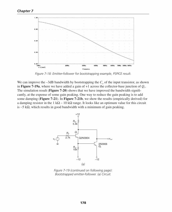
Chapter 7
178
Figure 7-18: Emitter-follower for bootstrapping example, PSPICE result.
We can improve the –3dB bandwidth by bootstrapping the Cμ of the input transistor, as shown in Figure 7-19a, where we have added a gain of +1 across the collector-base junction of Q1. The simulation result (Figure 7-20) shows that we have improved the bandwidth signifi -cantly, at the expense of some gain peaking. One way to reduce the gain peaking is to add some damping (Figure 7-21). In Figure 7-21b, we show the results (empirically derived) for a damping resistor in the 1 kΩ – 10 kΩ range. It looks like an optimum value for this circuit is ∼5 kΩ, which results in good bandwidth with a minimum of gain peaking.
(a)
Figure 7-19 (continued on following page): Bootstrapped emitter-follower. (a) Circuit.
+–
+12
Q2N3904
RS
2.7kvin
Re110k
vout
–12 –12
Q1
2N3906Q2
Re2
5.4k
Thompson Book.indb 178 3/20/2006 11:35:07 AM
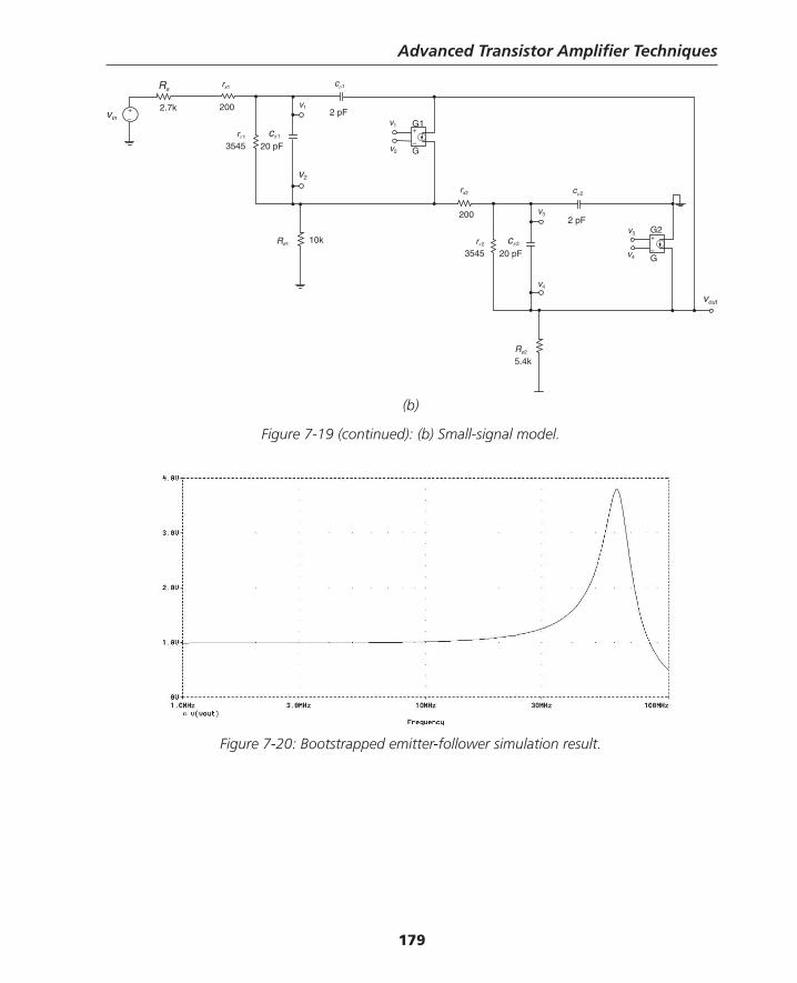
Advanced Transistor Amplifi er Techniques
179
(b)
Figure 7-19 (continued): (b) Small-signal model.
Figure 7-20: Bootstrapped emitter-follower simulation result.
rx1Rs
vout
cμ1
2.7k 200
G
2 pFG1
+–
v2
v1
v1
v2
Re1 10k
cπ1
20 pFrπ1
3545
vin
+
–
2 pF
rx2
v3
v4
v3
v4 G
G2+
–
Re2
5.4k
cμ2
cπ2
20 pFrπ2
3545
200
Thompson Book.indb 179 3/20/2006 11:35:08 AM
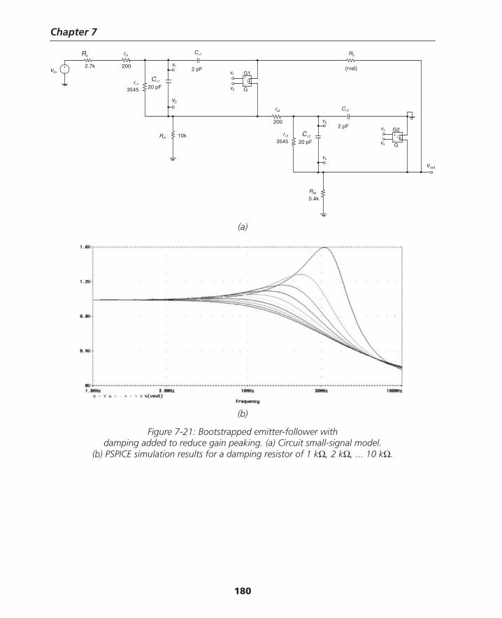
Chapter 7
180
(a)
(b)
Figure 7-21: Bootstrapped emitter-follower with damping added to reduce gain peaking. (a) Circuit small-signal model.
(b) PSPICE simulation results for a damping resistor of 1 kΩ, 2 kΩ, ... 10 kΩ.
rx1Rs
vout
Cμ1
2.7k 200
G
2 pFG1
+–
v2
v1
v1
v2
Re1 10k
Cπ1
20 pFrπ1
3545
vin+
–
2 pF
rx2
v3
v4
v3
v4 G
G2+
–
Re2
5.4k
Cμ2
Cπ2
20 pF
rπ2
3545
200
R3
{rval}
Thompson Book.indb 180 3/20/2006 11:35:08 AM
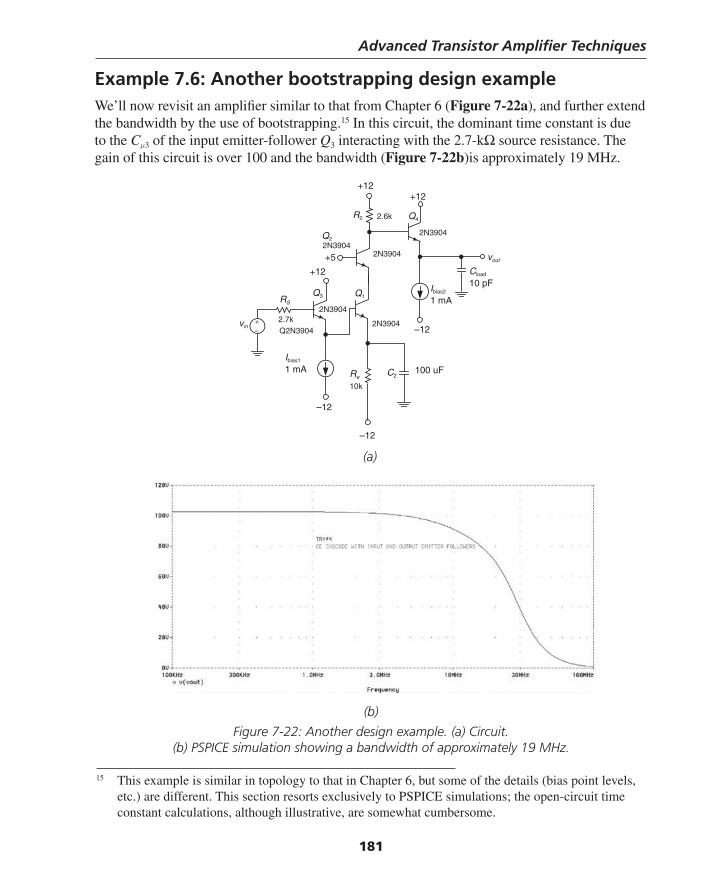
Advanced Transistor Amplifi er Techniques
181
Example 7.6: Another bootstrapping design exampleWe’ll now revisit an amplifi er similar to that from Chapter 6 (Figure 7-22a), and further extend the bandwidth by the use of bootstrapping.15 In this circuit, the dominant time constant is due to the Cμ3 of the input emitter-follower Q3 interacting with the 2.7-kΩ source resistance. The gain of this circuit is over 100 and the bandwidth (Figure 7-22b)is approximately 19 MHz.
(a)
15 This example is similar in topology to that in Chapter 6, but some of the details (bias point levels, etc.) are different. This section resorts exclusively to PSPICE simulations; the open-circuit time constant calculations, although illustrative, are somewhat cumbersome.
+–
+12
Q2N3904
RS
2.7k
Cload
10 pF
Re
10k
vout
–12
Q1
2N3904
C2
2.6k
Q3
Q4
+12+12
–12
–12
R2
Ibias2
1 mA
2N39042N3904Q2
+5
100 uFIbias1
1 mA
vin
2N3904
2N3904
(b)
Figure 7-22: Another design example. (a) Circuit. (b) PSPICE simulation showing a bandwidth of approximately 19 MHz.
Thompson Book.indb 181 3/20/2006 11:35:09 AM
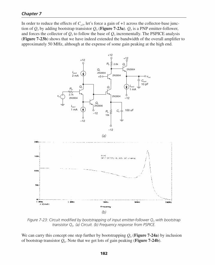
Chapter 7
182
In order to reduce the effects of Cμ3, let’s force a gain of +1 across the collector-base junc-tion of Q3 by adding bootstrap transistor Q5 (Figure 7-23a). Q5 is a PNP emitter-follower, and forces the collector of Q3 to follow the base of Q3 incrementally. The PSPICE analysis (Figure 7-23b) shows that we have indeed extended the bandwidth of the overall amplifi er to approximately 50 MHz, although at the expense of some gain peaking at the high end.
(a)
(b)
Figure 7-23: Circuit modifi ed by bootstrapping of input emitter-follower Q3 with bootstrap transistor Q5. (a) Circuit. (b) Frequency response from PSPICE.
We can carry this concept one step further by bootstrapping Q4 (Figure 7-24a) by inclusion of bootstrap transistor Q6. Note that we get lots of gain peaking (Figure 7-24b).
+–
+12
2N3904
RS
2.7k
Cload
10 pF
Re
10k
vout
–12
Q1
2N3904
C2
2.6k
Q3
Q4
+12+12
–12
–12
R2
Ibias2
1 mA
2N39042N3904Q2
+5
100 uF
Ibias1
1 mA
vin
Ibias3
2 mA
–12
2N3906Q5
2N3904
Thompson Book.indb 182 3/20/2006 11:35:10 AM
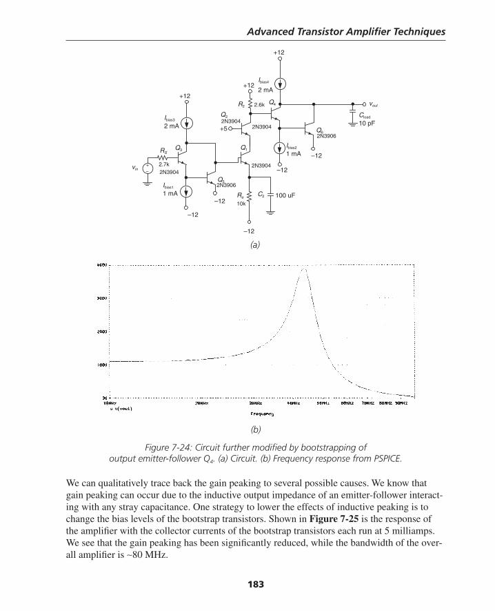
Advanced Transistor Amplifi er Techniques
183
(a)
(b)
Figure 7-24: Circuit further modifi ed by bootstrapping of output emitter-follower Q4. (a) Circuit. (b) Frequency response from PSPICE.
We can qualitatively trace back the gain peaking to several possible causes. We know that gain peaking can occur due to the inductive output impedance of an emitter-follower interact-ing with any stray capacitance. One strategy to lower the effects of inductive peaking is to change the bias levels of the bootstrap transistors. Shown in Figure 7-25 is the response of the amplifi er with the collector currents of the bootstrap transistors each run at 5 milliamps. We see that the gain peaking has been signifi cantly reduced, while the bandwidth of the over-all amplifi er is ∼80 MHz.
+–
+12
2N3904
RS
2.7k
Cload
10 pF
Re
10k
vout
–12
Q1
2N3904
C2
2.6k
+12
+12
–12
–12
R2
Ibias2
1 mA
2N39042N3904Q2
+5
100 uF
Ibias1
1 mA
vin
Ibias3
2 mA
2N3906Q5
–12
Ibias4
2 mA
2N3906Q6
Q4
–12Q3
Thompson Book.indb 183 3/20/2006 11:35:10 AM
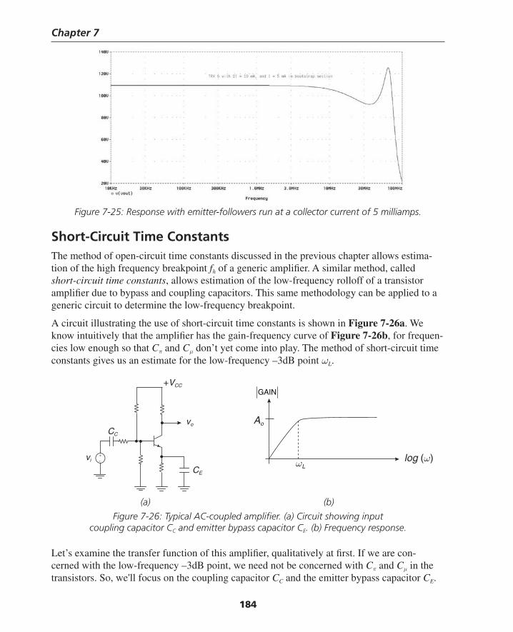
Chapter 7
184
Figure 7-25: Response with emitter-followers run at a collector current of 5 milliamps.
Short-Circuit Time ConstantsThe method of open-circuit time constants discussed in the previous chapter allows estima-tion of the high frequency breakpoint fh of a generic amplifi er. A similar method, called short-circuit time constants, allows estimation of the low-frequency rolloff of a transistor amplifi er due to bypass and coupling capacitors. This same methodology can be applied to a generic circuit to determine the low-frequency breakpoint.
A circuit illustrating the use of short-circuit time constants is shown in Figure 7-26a. We know intuitively that the amplifi er has the gain-frequency curve of Figure 7-26b, for frequen-cies low enough so that Cπ and Cμ don’t yet come into play. The method of short-circuit time constants gives us an estimate for the low-frequency –3dB point ωL.
CE
log (ω)ωL
Ao
GAIN
CC
vo
vi+–
+VCC
(a) (b)
Figure 7-26: Typical AC-coupled amplifi er. (a) Circuit showing input coupling capacitor CC and emitter bypass capacitor CE. (b) Frequency response.
Let’s examine the transfer function of this amplifi er, qualitatively at fi rst. If we are con-cerned with the low-frequency –3dB point, we need not be concerned with Cπ and Cμ in the transistors. So, we'll focus on the coupling capacitor CC and the emitter bypass capacitor CE.
Thompson Book.indb 184 3/20/2006 11:35:11 AM
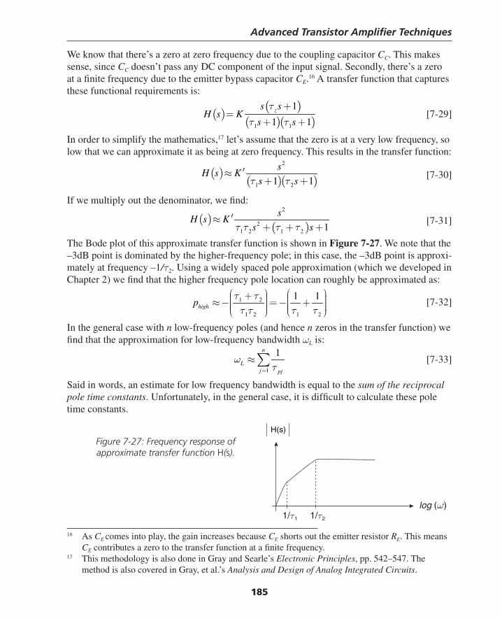
Advanced Transistor Amplifi er Techniques
185
We know that there’s a zero at zero frequency due to the coupling capacitor CC. This makes sense, since CC doesn’t pass any DC component of the input signal. Secondly, there’s a zero at a fi nite frequency due to the emitter bypass capacitor CE.16 A transfer function that captures these functional requirements is:
( )( )
( )( )1 1
1
1 1zs s
H s Ks s
τ
τ τ
+=
+ + [7-29]
In order to simplify the mathematics,17 let’s assume that the zero is at a very low frequency, so low that we can approximate it as being at zero frequency. This results in the transfer function:
( )( )( )
2
1 21 1
sH s K
s sτ τ′≈
+ + [7-30]
If we multiply out the denominator, we fi nd:
( )( )
2
21 2 1 2 1
sH s K
s sτ τ τ τ′≈
+ + + [7-31]
The Bode plot of this approximate transfer function is shown in Figure 7-27. We note that the –3dB point is dominated by the higher-frequency pole; in this case, the –3dB point is approxi-mately at frequency –1/τ2. Using a widely spaced pole approximation (which we developed in Chapter 2) we fi nd that the higher frequency pole location can roughly be approximated as:
1 2
1 2 1 2
1 1highp
τ ττ τ τ τ
⎛ ⎞ ⎛ ⎞+ ⎟ ⎟⎜ ⎜⎟ ⎟≈ − = − +⎜ ⎜⎟ ⎟⎜ ⎜⎟ ⎟⎜ ⎜⎝ ⎠ ⎝ ⎠ [7-32]
In the general case with n low-frequency poles (and hence n zeros in the transfer function) we fi nd that the approximation for low-frequency bandwidth ωL is:
1
1n
Lj pj
ωτ=
≈ ∑ [7-33]
Said in words, an estimate for low frequency bandwidth is equal to the sum of the reciprocal pole time constants. Unfortunately, in the general case, it is diffi cult to calculate these pole time constants.
log (ω)
H(s)
1/τ1 1/τ2
Figure 7-27: Frequency response of approximate transfer function H(s).
16 As CE comes into play, the gain increases because CE shorts out the emitter resistor RE. This means CE contributes a zero to the transfer function at a fi nite frequency.
17 This methodology is also done in Gray and Searle’s Electronic Principles, pp. 542–547. The method is also covered in Gray, et al.’s Analysis and Design of Analog Integrated Circuits.
Thompson Book.indb 185 3/20/2006 11:35:11 AM
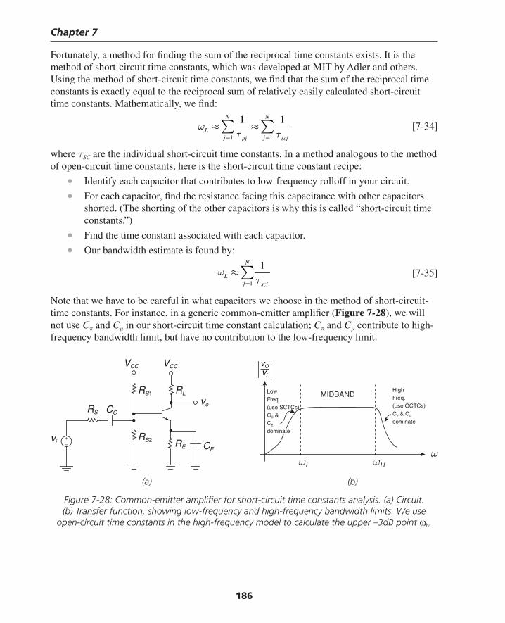
Chapter 7
186
Fortunately, a method for fi nding the sum of the reciprocal time constants exists. It is the method of short-circuit time constants, which was developed at MIT by Adler and others. Using the method of short-circuit time constants, we fi nd that the sum of the reciprocal time constants is exactly equal to the reciprocal sum of relatively easily calculated short-circuit time constants. Mathematically, we fi nd:
1 1
1 1N N
Lj jpj scj
ωτ τ= =
≈ ≈∑ ∑ [7-34]
where τSC are the individual short-circuit time constants. In a method analogous to the method of open-circuit time constants, here is the short-circuit time constant recipe:
• Identify each capacitor that contributes to low-frequency rolloff in your circuit.
• For each capacitor, fi nd the resistance facing this capacitance with other capacitors shorted. (The shorting of the other capacitors is why this is called “short-circuit time constants.”)
• Find the time constant associated with each capacitor.
• Our bandwidth estimate is found by:
1
1N
Lj scj
ωτ=
≈ ∑ [7-35]
Note that we have to be careful in what capacitors we choose in the method of short-circuit-time constants. For instance, in a generic common-emitter amplifi er (Figure 7-28), we will not use Cπ and Cμ in our short-circuit time constant calculation; Cπ and Cμ contribute to high-frequency bandwidth limit, but have no contribution to the low-frequency limit.
(a) (b)
Figure 7-28: Common-emitter amplifi er for short-circuit time constants analysis. (a) Circuit. (b) Transfer function, showing low-frequency and high-frequency bandwidth limits. We use
open-circuit time constants in the high-frequency model to calculate the upper –3dB point ωh.
ωωL ωH
CE
CC
vo
vi+–
VCC VCC
RS
RE
RLRB1
RB2
vO
vi
MIDBANDHighFreq.(use OCTCs)Cπ & Cμ
dominate
LowFreq.(use SCTCs)CC &CE
dominate
Thompson Book.indb 186 3/20/2006 11:35:12 AM
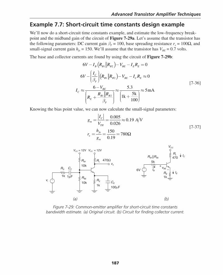
Advanced Transistor Amplifi er Techniques
187
Example 7.7: Short-circuit time constants design exampleWe’ll now do a short-circuit time constants example, and estimate the low-frequency break-point and the midband gain of the circuit of Figure 7-29a. Let’s assume that the transistor has the following parameters: DC current gain βF = 100, base spreading resistance rx = 100Ω, and small-signal current gain hfe = 150. We’ll assume that the transistor has VBE = 0.7 volts.
The base and collector currents are found by using the circuit of Figure 7-29b:
( )
( )
1 2
1 2
1 2
6 0
6 0
6 5.35mA
5k1k
100
B B B BE E E
CB B BE C E
F
BEC
B BE
F
V I R R V I R
IV R R V I R
VI
R RR
β
β
− − − =
⎛ ⎞⎟⎜ ⎟− − − ≈⎜ ⎟⎜ ⎟⎜⎝ ⎠
−≈ ≈ ≈
⎛ ⎞ ⎛ ⎞⎟ ⎟⎜ ⎜ +⎟ ⎟+⎜ ⎜⎟ ⎟⎜⎜ ⎝ ⎠⎟⎜⎝ ⎠
[7-36]
Knowing the bias point value, we can now calculate the small-signal parameters:
0.0050.19
0.026
150780
0.19
Cm
TH
fe
m
Ig A V
V
hr
gπ
= = ≈
= = = Ω [7-37]
CE
100μF
CC
vo
vi+–
VCC = 12V VCC = 12V
RS
RE
1k
RLRB1
10k
RB2
10k
1k 1μF
470Ω
IE
vBE+–
VCC
RE
1k
RLRB1||RB2
5k470
IC
IB
+–6V
(a) (b)
Figure 7-29: Common-emitter amplifi er for short-circuit time constants bandwidth estimate. (a) Original circuit. (b) Circuit for fi nding collector current.
Thompson Book.indb 187 3/20/2006 11:35:12 AM
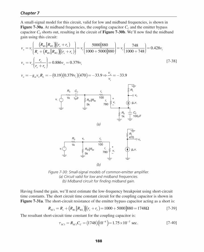
Chapter 7
188
A small-signal model for this circuit, valid for low and midband frequencies, is shown in Figure 7-30a. At midband frequencies, the coupling capacitor CC and the emitter bypass capacitor CE shorts out, resulting in the circuit of Figure 7-30b. We’ll now fi nd the midband gain using this circuit:
( )( )( )( )
( )( )( )
1 2
1 2
5000 880 7480.428
1000 5000 880 1000 748
0.886 0.379
0.19 0.379 470 33.9 33.9
B B x
x i i i i
s B B x
x x ix
oo m L i
i
R R r rv v v v v
R R R r r
rv v v v
r r
vv g v R v
v
π
π
ππ
π
π
⎛ ⎞ ⎛ ⎞+ ⎛ ⎞⎟⎜ ⎟⎜⎟ ⎟⎜⎜ ⎟⎜= = = =⎟ ⎟⎜⎟⎜ ⎜⎟ ⎟⎜⎟⎜ ⎟ ⎝ ⎠⎜⎟ + ++ + ⎟⎜ ⎝ ⎠⎝ ⎠⎛ ⎞⎟⎜ ⎟= = =⎜ ⎟⎜ ⎟⎜ +⎝ ⎠
= − = − = − ⇒ = −
[7-38]
CC
vi+–
RS
RE
1k
RL
RB1 RB2
5k
1k 1μF
rx
vπrπ
780
+
–
CE
100μF
vo
gmvπ
100
vi+–
RS
1k
vπ
rπ
780
+
–
rxvx
100
RL
470vo
gmvπRB1 RB2
5k
(a)
(b)
Figure 7-30: Small-signal models of common-emitter amplifi er. (a) Circuit valid for low and midband frequencies.
(b) Midband circuit for fi nding midband gain.
Having found the gain, we’ll next estimate the low-frequency breakpoint using short-circuit time constants. The short circuit time constant circuit for the coupling capacitor is shown in Figure 7-31a. The short-circuit resistance of the emitter bypass capacitor acting as a short is:
( )( )1 1 2 1000 5000 880 1748SC s B B xR R R R r rπ= + + = + = Ω [7-39]
The resultant short-circuit time constant for the coupling capacitor is:
( )( )6 31 1 1748 10 1.75 10 sec.SC SC CR Cτ − −= = = × [7-40]
Thompson Book.indb 188 3/20/2006 11:35:13 AM
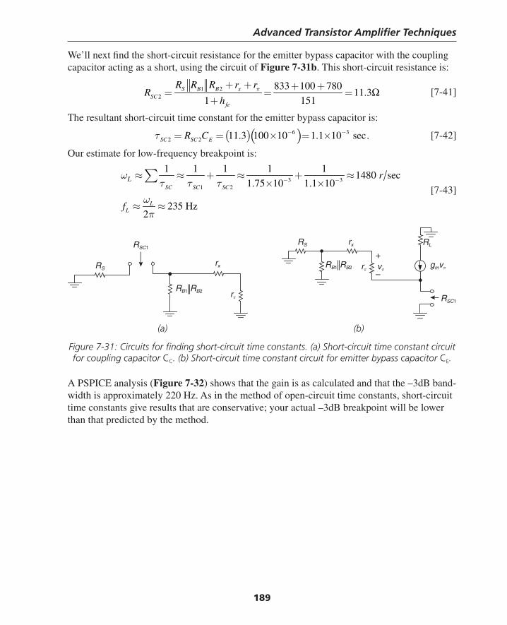
Advanced Transistor Amplifi er Techniques
189
We’ll next fi nd the short-circuit resistance for the emitter bypass capacitor with the coupling capacitor acting as a short, using the circuit of Figure 7-31b. This short-circuit resistance is:
1 22
833 100 78011.3
1 151S B B x
SCfe
R R R r rR
hπ+ + + +
= = =+
Ω [7-41]
The resultant short-circuit time constant for the emitter bypass capacitor is:
( )( )6 32 2 11.3 100 10 1.1 10 sec.SC SC ER Cτ − −= = × = × [7-42]
Our estimate for low-frequency breakpoint is:
3 3
1 2
1 1 1 1 11480 sec
1.75 10 1.1 10
235 Hz2
SC SC SC
LL
L r
f
ωτ τ τ
ωπ
− −≈ ≈ + ≈ + ≈× ×
≈ ≈
∑ [7-43]
(a) (b)
Figure 7-31: Circuits for fi nding short-circuit time constants. (a) Short-circuit time constant circuit for coupling capacitor CC. (b) Short-circuit time constant circuit for emitter bypass capacitor CE.
A PSPICE analysis (Figure 7-32) shows that the gain is as calculated and that the –3dB band-width is approximately 220 Hz. As in the method of open-circuit time constants, short-circuit time constants give results that are conservative; your actual –3dB breakpoint will be lower than that predicted by the method.
RL
vπ
+
–gmvπ
RB1 RB2
rx
rπ
RS
RSC1rxRS
RB1 RB2
RSC1
rπ
Thompson Book.indb 189 3/20/2006 11:35:13 AM
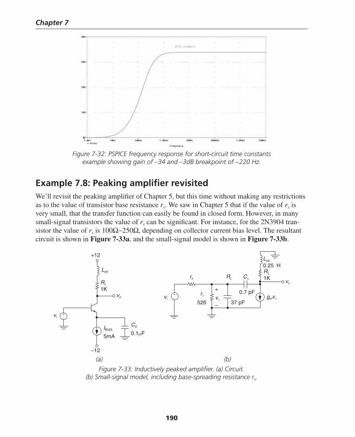
Chapter 7
190
Figure 7-32: PSPICE frequency response for short-circuit time constants example showing gain of –34 and –3dB breakpoint of ∼220 Hz.
Example 7.8: Peaking amplifi er revisitedWe’ll revisit the peaking amplifi er of Chapter 5, but this time without making any restrictions as to the value of transistor base resistance rx. We saw in Chapter 5 that if the value of rx is very small, that the transfer function can easily be found in closed form. However, in many small-signal transistors the value of rx can be signifi cant. For instance, for the 2N3904 tran-sistor the value of rx is 100Ω∼250Ω, depending on collector current bias level. The resultant circuit is shown in Figure 7-33a, and the small-signal model is shown in Figure 7-33b.
CE
0.1μF
Cμ
vo+–
RL
1K
+–
Lpk
vi
vi
Lpk
0.25 H
IBIAS
5mA
vo
rx RL
RL
1K
+12
–12
rπ vπ526 37 pF
0.7 pFgmvπ
+
–
(a) (b)
Figure 7-33: Inductively peaked amplifi er. (a) Circuit. (b) Small-signal model, including base-spreading resistance rx.
Thompson Book.indb 190 3/20/2006 11:35:14 AM
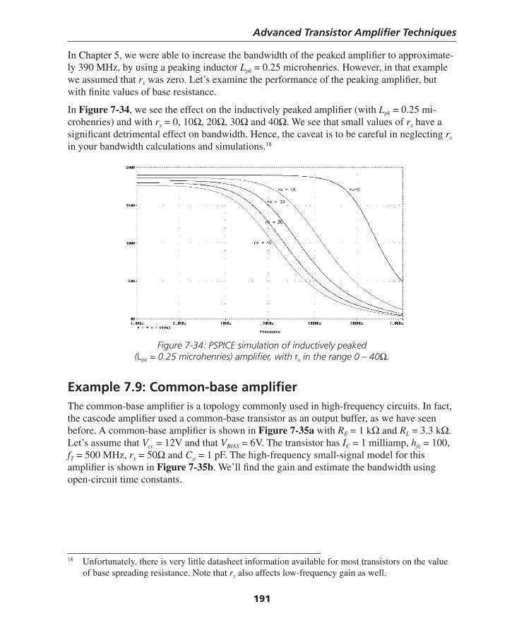
Advanced Transistor Amplifi er Techniques
191
In Chapter 5, we were able to increase the bandwidth of the peaked amplifi er to approximate-ly 390 MHz, by using a peaking inductor Lpk = 0.25 microhenries. However, in that example we assumed that rx was zero. Let’s examine the performance of the peaking amplifi er, but with fi nite values of base resistance.
In Figure 7-34, we see the effect on the inductively peaked amplifi er (with Lpk = 0.25 mi-crohenries) and with rx = 0, 10Ω, 20Ω, 30Ω and 40Ω. We see that small values of rx have a signifi cant detrimental effect on bandwidth. Hence, the caveat is to be careful in neglecting rx in your bandwidth calculations and simulations.18
18 Unfortunately, there is very little datasheet information available for most transistors on the value of base spreading resistance. Note that rx also affects low-frequency gain as well.
Figure 7-34: PSPICE simulation of inductively peaked (Lpk = 0.25 microhenries) amplifi er, with rx in the range 0 – 40Ω.
Example 7.9: Common-base amplifi erThe common-base amplifi er is a topology commonly used in high-frequency circuits. In fact, the cascode amplifi er used a common-base transistor as an output buffer, as we have seen before. A common-base amplifi er is shown in Figure 7-35a with RE = 1 kΩ and RL = 3.3 kΩ. Let’s assume that Vcc = 12V and that VBIAS = 6V. The transistor has IC = 1 milliamp, hfe = 100, fT = 500 MHz, rx = 50Ω and Cμ = 1 pF. The high-frequency small-signal model for this amplifi er is shown in Figure 7-35b. We’ll fi nd the gain and estimate the bandwidth using open-circuit time constants.
Thompson Book.indb 191 3/20/2006 11:35:14 AM
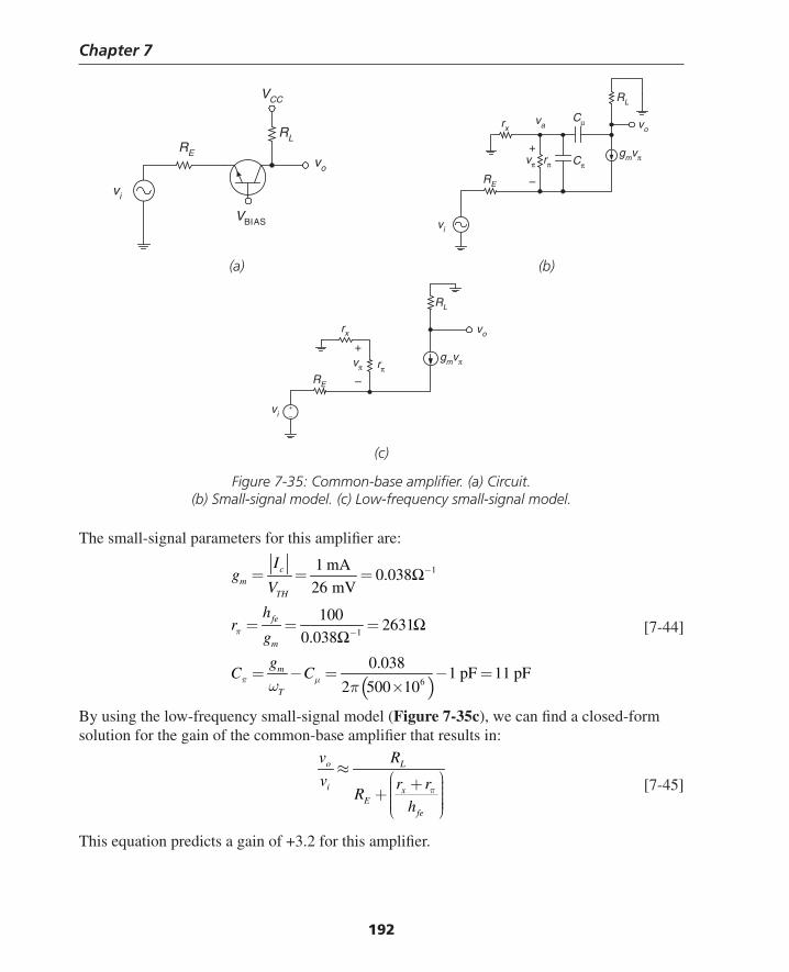
Chapter 7
192
(a) (b)
vo
VBIAS
vi
VCC
RE
RL+
–
rx
rπ Cπ
Cμ
gmvπvπ
vova
RL
RE
vi
+
–
rx
rπvπ
vo
RL
RE
vi+–
gmvπ
(c)
Figure 7-35: Common-base amplifi er. (a) Circuit. (b) Small-signal model. (c) Low-frequency small-signal model.
The small-signal parameters for this amplifi er are:
( )
1
1
6
1 mA0.038
26 mV
1002631
0.038
0.0381 pF 11 pF
2 500 10
cm
TH
fe
m
m
T
Ig
V
hr
g
gC C
π
π μω π
−
−
= = =
= = =
= − = − =×
Ω
ΩΩ [7-44]
By using the low-frequency small-signal model (Figure 7-35c), we can fi nd a closed-form solution for the gain of the common-base amplifi er that results in:
o L
i xE
fe
v R
v r rR
hπ
≈⎛ ⎞+ ⎟⎜ ⎟⎜+ ⎟⎜ ⎟⎟⎜⎝ ⎠
[7-45]
This equation predicts a gain of +3.2 for this amplifi er.
Thompson Book.indb 192 3/20/2006 11:35:15 AM
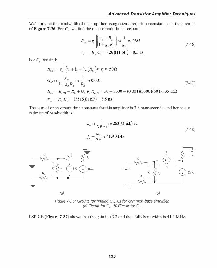
Advanced Transistor Amplifi er Techniques
193
We’ll predict the bandwidth of the amplifi er using open-circuit time constants and the circuits of Figure 7-36. For Cπ, we fi nd the open-circuit time constant:
( )( )
126
1
26 11 pF 0.3 ns
x Eo
m E m
o o
r RR r
g R g
R C
π π
π π πτ
⎛ ⎞+ ⎟⎜ ⎟= ≈ ≈⎜ ⎟⎜ ⎟⎜ +⎝ ⎠
= = =
Ω [7-46]
For Cμ, we fi nd:
( )( )
( )( )( )( )( )
1
1 1
1 50
10.001
1
50 3300 0.001 3300 50 3515
3515 1 pF 3.5 ns
EQ x fe E x
mM
m E E
o EQ L M L EQ
o o
R r r h R r
gG
g R R
R R R G R R
R C
π
μ
μ μ μτ
= + + ≈ ≈
≈ ≈ ≈+
= + + = + + ≈
= = =
Ω
Ω
[7-47]
The sum of open-circuit time constants for this amplifi er is 3.8 nanoseconds, and hence our estimate of bandwidth is:
1263 Mrad sec
3.8 ns
41.9 MHz2
h
hhf
ω
ωπ
≈ ≈
= ≈
[7-48]
RL
vπ gmvπrπ
+
–
vt
it
+–
RE
rx RL
vπ gmvπrπ
+
–
vt
it
RE
rx
+ –
(a) (b)
Figure 7-36: Circuits for fi nding OCTCs for common-base amplifi er. (a) Circuit for Cπ. (b) Circuit for Cµ.
PSPICE (Figure 7-37) shows that the gain is +3.2 and the –3dB bandwidth is 44.4 MHz.
Thompson Book.indb 193 3/20/2006 11:35:15 AM
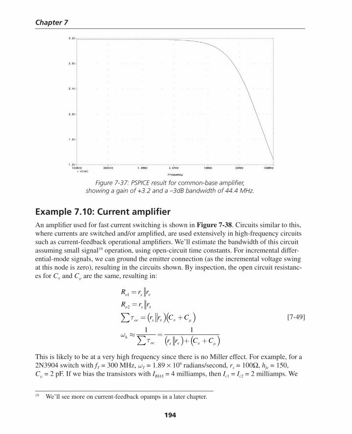
Chapter 7
194
Figure 7-37: PSPICE result for common-base amplifi er, showing a gain of +3.2 and a –3dB bandwidth of 44.4 MHz.
Example 7.10: Current amplifi erAn amplifi er used for fast current switching is shown in Figure 7-38. Circuits similar to this, where currents are switched and/or amplifi ed, are used extensively in high-frequency circuits such as current-feedback operational amplifi ers. We’ll estimate the bandwidth of this circuit assuming small signal19 operation, using open-circuit time constants. For incremental differ-ential-mode signals, we can ground the emitter connection (as the incremental voltage swing at this node is zero), resulting in the circuits shown. By inspection, the open circuit resistanc-es for Cπ and Cμ are the same, resulting in:
( )( )
( ) ( )
1
2
1 1
o x
o x
oc x
hoc x
R r r
R r r
r r C C
r r C C
π
π
π π μ
π π μ
τ
ωτ
=
=
= +
≈ =+ +
∑
∑
[7-49]
This is likely to be at a very high frequency since there is no Miller effect. For example, for a 2N3904 switch with fT = 300 MHz, ωT = 1.89 × 10⁹ radians/second, rx = 100Ω, hfe = 150, Cμ = 2 pF. If we bias the transistors with IBIAS = 4 milliamps, then Ic1 = Ic2 = 2 milliamps. We
19 We’ll see more on current-feedback opamps in a later chapter.
Thompson Book.indb 194 3/20/2006 11:35:16 AM
Advanced Transistor Amplifi er Techniques
195
then fi nd that Cπ = 38.8 pF, and rπ = 1950Ω. This results in an open-circuit time constant estimate of bandwidth ωh ≈ 257 Mrad/sec (fh ≈ 41 MHz). SPICE (Figure 7-39) shows fh = 41.5 MHz, so the estimate is pretty good.
(a) (b)
–VEE
IBIAS
IiBIASc2
+I
iBIASc2
−
V vB b+ V vB b−
Q1Q2
+
–
rx
rπ Cπ
Cμ
gmvπvπ
vo
vi
g vm π+–
vtrπvπ
+
– it
rx
g vm π
vt
rπvπ
+
–
itrx
+ –
(c) (d)
Figure 7-38: Current switching amplifi er. (a) Circuit. (b) High-frequency model. (c) Circuit for fi nding Cπ OCTC. (d) Circuit for fi nding Cμ OCTC.
Thompson Book.indb 195 3/20/2006 11:35:16 AM
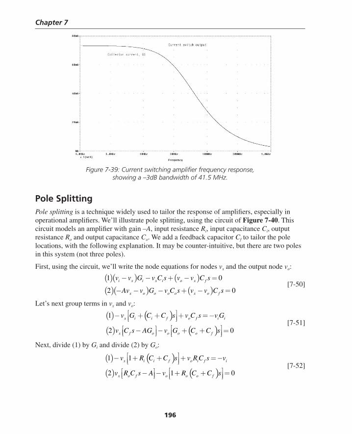
Chapter 7
196
Figure 7-39: Current switching amplifi er frequency response,showing a –3dB bandwidth of 41.5 MHz.
Pole SplittingPole splitting is a technique widely used to tailor the response of amplifi ers, especially in operational amplifi ers. We’ll illustrate pole splitting, using the circuit of Figure 7-40. This circuit models an amplifi er with gain –A, input resistance Ri, input capacitance Ci, output resistance Ro and output capacitance Co. We add a feedback capacitor Cf to tailor the pole locations, with the following explanation. It may be counter-intuitive, but there are two poles in this system (not three poles).
First, using the circuit, we’ll write the node equations for nodes vx and the output node vo:
( )( ) ( )( )( ) ( )1 0
2 0
i x i x i o x f
x o o o o x o f
v v G v C s v v C s
Av v G v C s v v C s
− − + − =
− − − + − = [7-50]
Let’s next group terms in vx and vo:
( ) ( )( ) ( )
1
2 0
x i i f o f i i
x f o o o o f
v G C C s v C s v G
v C s AG v G C C s
⎡ ⎤− + + + = −⎢ ⎥⎣ ⎦⎡ ⎤⎡ ⎤− − + + =⎢ ⎥ ⎢ ⎥⎣ ⎦ ⎣ ⎦
[7-51]
Next, divide (1) by Gi and divide (2) by Go:
( ) ( )( ) ( )
1 1
2 1 0
x i i f o i f i
x o f o o o f
v R C C s v R C s v
v R C s A v R C C s
⎡ ⎤− + + + = −⎢ ⎥⎣ ⎦⎡ ⎤⎡ ⎤− − + + =⎢ ⎥ ⎢ ⎥⎣ ⎦ ⎣ ⎦
[7-52]
Thompson Book.indb 196 3/20/2006 11:35:17 AM
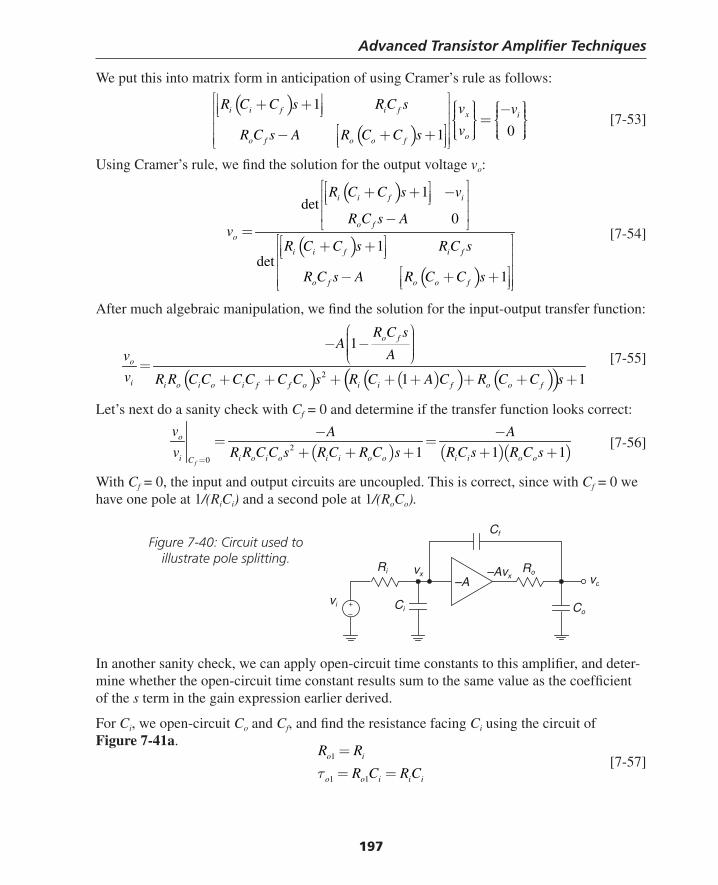
Advanced Transistor Amplifi er Techniques
197
We put this into matrix form in anticipation of using Cramer’s rule as follows:
( )
( )
1
01
i i f i f x i
oo f o o f
R C C s R C s v v
vR C s A R C C s
⎡ ⎤⎢ ⎥+ + ⎧ ⎫ ⎧ ⎫⎢ ⎥ −⎪ ⎪⎢ ⎥ ⎪ ⎪⎣ ⎦ ⎪ ⎪ ⎪ ⎪⎢ ⎥ =⎨ ⎬ ⎨ ⎬⎪ ⎪ ⎪ ⎪⎢ ⎥⎡ ⎤− + + ⎪ ⎪⎩ ⎭⎪ ⎪⎩ ⎭⎢ ⎥⎢ ⎥⎣ ⎦⎣ ⎦
[7-53]
Using Cramer’s rule, we fi nd the solution for the output voltage vo:
( )
( )( )
1det
0
1det
1
i i f i
o f
o
i i f i f
o f o o f
R C C s v
R C s Av
R C C s R C s
R C s A R C C s
⎡ ⎤⎡ ⎤+ + −⎢ ⎥⎢ ⎥⎣ ⎦⎢ ⎥⎢ ⎥−⎣ ⎦=
⎡ ⎤⎡ ⎤+ +⎢ ⎥⎢ ⎥⎣ ⎦⎢ ⎥⎢ ⎥⎡ ⎤− + +⎢ ⎥⎢ ⎥⎣ ⎦⎣ ⎦
[7-54]
After much algebraic manipulation, we fi nd the solution for the input-output transfer function:
( ) ( )( ) ( )( )2
1
1 1
o f
o
i i o i o i f f o i i f o o f
R C sA
Av
v R R C C C C C C s R C A C R C C s
⎛ ⎞⎟⎜ ⎟− −⎜ ⎟⎜ ⎟⎜⎝ ⎠=
+ + + + + + + + [7-55]
Let’s next do a sanity check with Cf = 0 and determine if the transfer function looks correct:
( ) ( )( )2
01 11
f
o
i i i o oi o i o i i o oC
v A A
v R C s R C sR R C C s R C R C s=
− −= =
+ ++ + + [7-56]
With Cf = 0, the input and output circuits are uncoupled. This is correct, since with Cf = 0 we have one pole at 1/(RiCi) and a second pole at 1/(RoCo).
In another sanity check, we can apply open-circuit time constants to this amplifi er, and deter-mine whether the open-circuit time constant results sum to the same value as the coeffi cient of the s term in the gain expression earlier derived.
For Ci, we open-circuit Co and Cf, and fi nd the resistance facing Ci using the circuit of Figure 7-41a.
1
1 1
o i
o o i i i
R R
R C R Cτ
=
= = [7-57]
Co
vo
Civi
vx
+–
Ri
Cf
Ro–Avx–A
Figure 7-40: Circuit used to illustrate pole splitting.
Thompson Book.indb 197 3/20/2006 11:35:17 AM
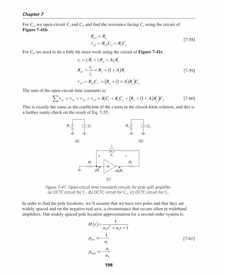
Chapter 7
198
For Co, we open-circuit Ci and Cf, and fi nd the resistance facing Co using the circuit of Figure 7-41b.
2
2 2
o o
o o o o o
R R
R C R Cτ
=
= = [7-58]
For Cf, we need to do a little bit more work using the circuit of Figure 7-41c.
( )
( )( )
3
3 3
1
1
t t i t o t i
to o i
t
o o f o i f
v i R i R Ai R
vR R A R
i
R C R A R Cτ
= + +
= = + +
= = + +
[7-59]
The sum of the open-circuit time constants is:
( )( )1 2 3 1oc o o o i i o o o i fR C R C R A R Cτ τ τ τ= + + = + + + +∑ [7-60]
This is exactly the same as the coeffi cient of the s term in the closed-form solution, and this is a further sanity check on the result of Eq. 7-55.
+ –
Ri Ro
–AitRi
Ri Ci Ro Co
itRi
it
vt
–A
(a) (b)
(c)
Figure 7-41: Open-circuit time constants circuits for pole split amplifi er. (a) OCTC circuit for Ci. (b) OCTC circuit for Co. (c) OCTC circuit for Cf.
In order to fi nd the pole locations, we’ll assume that we have two poles and that they are widely spaced and on the negative real axis, a circumstance that occurs often in wideband amplifi ers. Our widely spaced pole location approximation for a second-order system is:
( ) 22 1
1
1
2
1
1
1low
high
H sa s a s
pa
ap
a
=+ +
≈ −
≈ −
[7-61]
Thompson Book.indb 198 3/20/2006 11:35:18 AM
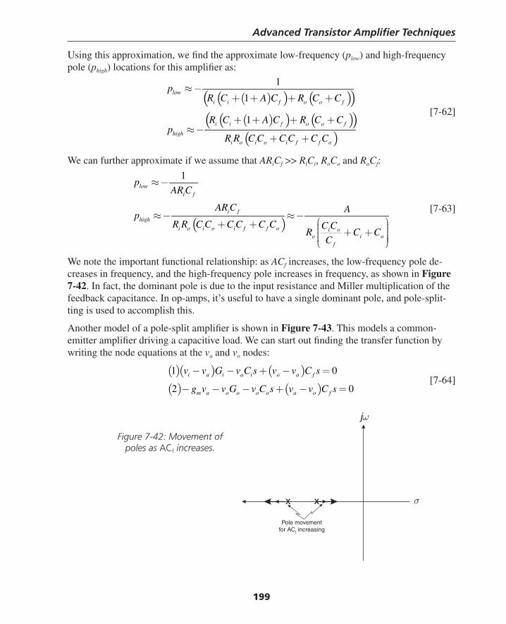
Advanced Transistor Amplifi er Techniques
199
Using this approximation, we fi nd the approximate low-frequency (plow) and high-frequency pole (phigh) locations for this amplifi er as:
( )( ) ( )( )( )( ) ( )( )( )
1
1
1
low
i i f o o f
i i f o o f
high
i o i o i f f o
pR C A C R C C
R C A C R C Cp
R R C C C C C C
≈ −+ + + +
+ + + +≈ −
+ +
[7-62]
We can further approximate if we assume that ARiCf >> RiCi, RoCo and RoCf:
( )
1low
i f
i fhigh
i o i o i f f o i oo i o
f
pAR C
AR C Ap
R R C C C C C C C CR C C
C
≈ −
≈ − ≈ −⎛ ⎞+ + ⎟⎜ ⎟⎜ + + ⎟⎜ ⎟⎟⎜⎝ ⎠
[7-63]
We note the important functional relationship: as ACf increases, the low-frequency pole de-creases in frequency, and the high-frequency pole increases in frequency, as shown in Figure 7-42. In fact, the dominant pole is due to the input resistance and Miller multiplication of the feedback capacitance. In op-amps, it’s useful to have a single dominant pole, and pole-split-ting is used to accomplish this.
Another model of a pole-split amplifi er is shown in Figure 7-43. This models a common-emitter amplifi er driving a capacitive load. We can start out fi nding the transfer function by writing the node equations at the va and vo nodes:
( )( ) ( )( ) ( )1 0
2 0
i a i a i o a f
m a o o o o a o f
v v G v C s v v C s
g v v G v C s v v C s
− − + − =
− − − + − = [7-64]
σ
jω
xx
Pole movementfor ACf increasing
Figure 7-42: Movement of poles as ACf increases.
Thompson Book.indb 199 3/20/2006 11:35:19 AM
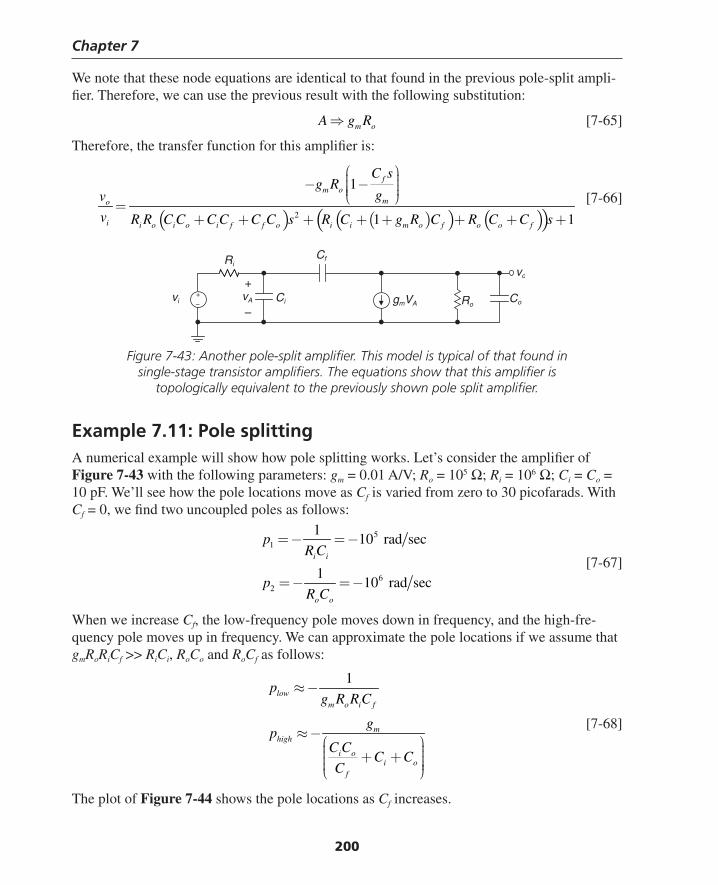
Chapter 7
200
We note that these node equations are identical to that found in the previous pole-split ampli-fi er. Therefore, we can use the previous result with the following substitution:
m oA g R⇒ [7-65]
Therefore, the transfer function for this amplifi er is:
( ) ( )( ) ( )( )2
1
1 1
fm o
mo
i i o i o i f f o i i m o f o o f
C sg R
gv
v R R C C C C C C s R C g R C R C C s
⎛ ⎞⎟⎜ ⎟− −⎜ ⎟⎜ ⎟⎜⎝ ⎠=
+ + + + + + + + [7-66]
Ri
Ro
vo+
–Co
vAvi Ci
Cf
gmVA+–
Figure 7-43: Another pole-split amplifi er. This model is typical of that found in single-stage transistor amplifi ers. The equations show that this amplifi er is
topologically equivalent to the previously shown pole split amplifi er.
Example 7.11: Pole splittingA numerical example will show how pole splitting works. Let’s consider the amplifi er of Figure 7-43 with the following parameters: gm = 0.01 A/V; Ro = 105 Ω; Ri = 106 Ω; Ci = Co = 10 pF. We’ll see how the pole locations move as Cf is varied from zero to 30 picofarads. With Cf = 0, we fi nd two uncoupled poles as follows:
51
62
110 rad sec
110 rad sec
i i
o o
pR C
pR C
= − = −
= − = − [7-67]
When we increase Cf, the low-frequency pole moves down in frequency, and the high-fre-quency pole moves up in frequency. We can approximate the pole locations if we assume that gmRoRiCf >> RiCi, RoCo and RoCf as follows:
1low
m o i f
mhigh
i oi o
f
pg R R C
gp
C CC C
C
≈ −
≈ −⎛ ⎞⎟⎜ ⎟⎜ + + ⎟⎜ ⎟⎟⎜⎝ ⎠
[7-68]
The plot of Figure 7-44 shows the pole locations as Cf increases.
Thompson Book.indb 200 3/20/2006 11:35:19 AM
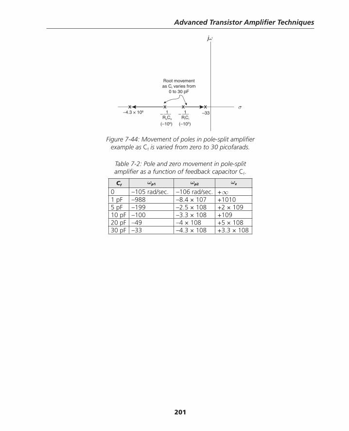
Advanced Transistor Amplifi er Techniques
201
Figure 7-44: Movement of poles in pole-split amplifi er example as Cf is varied from zero to 30 picofarads.
Table 7-2: Pole and zero movement in pole-split amplifi er as a function of feedback capacitor Cf.
Cfωp1 ωp2 ωz
0 –105 rad/sec. –106 rad/sec. +∞1 pF –988 –8.4 × 10⁷ +10105 pF –199 –2.5 × 10⁸ +2 × 10910 pF –100 –3.3 × 10⁸ +10920 pF –49 –4 × 10⁸ +5 × 10830 pF –33 –4.3 × 10⁸ +3.3 × 10⁸
σ
jω
Root movementas Cf varies from
0 to 30 pF
xxxx–4.3 × 10⁸ –33
(–106) (–105)
1RoCo
– 1RiCi
–
Thompson Book.indb 201 3/20/2006 11:35:20 AM
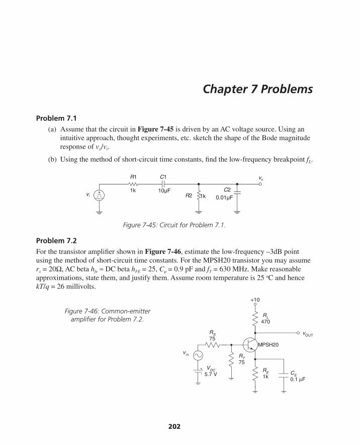
202
Chapter 7 Problems
Problem 7.1(a) Assume that the circuit in Figure 7-45 is driven by an AC voltage source. Using an
intuitive approach, thought experiments, etc. sketch the shape of the Bode magnitude response of vo/vi.
(b) Using the method of short-circuit time constants, fi nd the low-frequency breakpoint fL.
Figure 7-45: Circuit for Problem 7.1.
Problem 7.2For the transistor amplifi er shown in Figure 7-46, estimate the low-frequency –3dB point using the method of short-circuit time constants. For the MPSH20 transistor you may assume rx = 20Ω, AC beta hfe ≈ DC beta hFE = 25, Cµ = 0.9 pF and fT = 630 MHz. Make reasonable approximations, state them, and justify them. Assume room temperature is 25 oC and hence kT/q = 26 millivolts.
vo
vi
C1R1
C2R2
1k1k
10µF0.01µF
+–
MPSH20vin
vOUT
RL470
RE1k
+10
VDC5.7 V
RS75
CE0.1 μF
RT75
Figure 7-46: Common-emitter amplifi er for Problem 7.2.
Thompson Book.indb 202 3/20/2006 11:35:20 AM
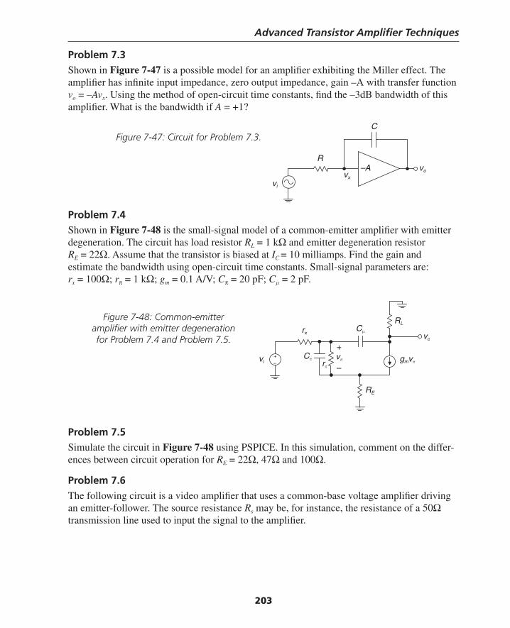
Advanced Transistor Amplifi er Techniques
203
Problem 7.3Shown in Figure 7-47 is a possible model for an amplifi er exhibiting the Miller effect. The amplifi er has infi nite input impedance, zero output impedance, gain –A with transfer function vo = –Avx. Using the method of open-circuit time constants, fi nd the –3dB bandwidth of this amplifi er. What is the bandwidth if A = +1?
Problem 7.4Shown in Figure 7-48 is the small-signal model of a common-emitter amplifi er with emitter degeneration. The circuit has load resistor RL = 1 kΩ and emitter degeneration resistor RE = 22Ω. Assume that the transistor is biased at IC = 10 milliamps. Find the gain and estimate the bandwidth using open-circuit time constants. Small-signal parameters are: rx = 100Ω; rπ = 1 kΩ; gm = 0.1 A/V; Cπ = 20 pF; Cμ = 2 pF.
Figure 7-48: Common-emitter amplifi er with emitter degeneration for Problem 7.4 and Problem 7.5.
vi
Rvo
vx
C
–A
RE
vo
+
–vi
Cπ gmvπ
Cμ
vπ
RL
rx
rπ
+–
Figure 7-47: Circuit for Problem 7.3.
Problem 7.5Simulate the circuit in Figure 7-48 using PSPICE. In this simulation, comment on the differ-ences between circuit operation for RE = 22Ω, 47Ω and 100Ω.
Problem 7.6The following circuit is a video amplifi er that uses a common-base voltage amplifi er driving an emitter-follower. The source resistance Rs may be, for instance, the resistance of a 50Ω transmission line used to input the signal to the amplifi er.
Thompson Book.indb 203 3/20/2006 11:35:20 AM
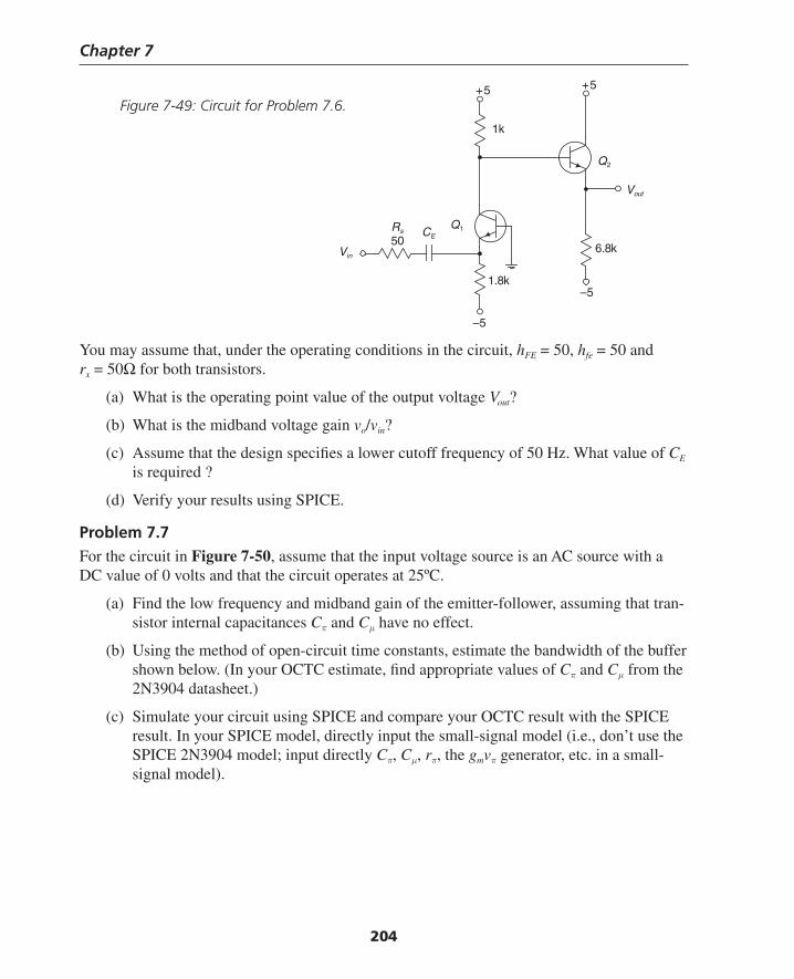
Chapter 7
204
You may assume that, under the operating conditions in the circuit, hFE = 50, hfe = 50 and rx = 50Ω for both transistors.
(a) What is the operating point value of the output voltage Vout?
(b) What is the midband voltage gain vo/vin?
(c) Assume that the design specifi es a lower cutoff frequency of 50 Hz. What value of CE is required ?
(d) Verify your results using SPICE.
Problem 7.7For the circuit in Figure 7-50, assume that the input voltage source is an AC source with a DC value of 0 volts and that the circuit operates at 25ºC.
(a) Find the low frequency and midband gain of the emitter-follower, assuming that tran-sistor internal capacitances Cπ and Cμ have no effect.
(b) Using the method of open-circuit time constants, estimate the bandwidth of the buffer shown below. (In your OCTC estimate, fi nd appropriate values of Cπ and Cμ from the 2N3904 datasheet.)
(c) Simulate your circuit using SPICE and compare your OCTC result with the SPICE result. In your SPICE model, directly input the small-signal model (i.e., don’t use the SPICE 2N3904 model; input directly Cπ, Cμ, rπ, the gmvπ generator, etc. in a small- signal model).
Vin
+5
Vout
Rs
50
1.8k
–5
CE
1k
+5
6.8k
–5
Q1
Q2
Figure 7-49: Circuit for Problem 7.6.
Thompson Book.indb 204 3/20/2006 11:35:21 AM
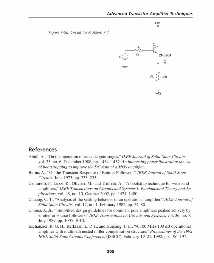
Advanced Transistor Amplifi er Techniques
205
ReferencesAbidi, A., “On the operation of cascode gain stages,” IEEE Journal of Solid-State Circuits,
vol. 23, no. 6, December 1988, pp. 1434–1437. An interesting paper illustrating the use of bootstrapping to improve the DC gain of a MOS amplifi er.
Barna, A., “On the Transient Response of Emitter Followers,” IEEE Journal of Solid-State Circuits, June 1973, pp. 233–235.
Centurelli, F., Luzzi, R., Olivieri, M., and Trifi letti, A., “A bootstrap technique for wideband amplifi ers,” IEEE Transactions on Circuits and Systems I: Fundamental Theory and Ap-plications, vol. 48, no. 10, October 2002, pp. 1474–1480.
Chuang, C. T., “Analysis of the settling behavior of an operational amplifi er,” IEEE Journal of Solid-State Circuits, vol. 17, no. 1, February 1982, pp. 74–80.
Choma, J., Jr., “Simplifi ed design guidelines for dominant pole amplifi ers peaked actively by emitter or source followers,” IEEE Transactions on Circuits and Systems, vol. 36, no. 7, July 1989, pp. 1005–1010.
Eschauzier, R. G. H., Kerklaan, L. P. T., and Huijsing, J. H., “A 100 MHz 100 dB operational amplifi er with multipath nested miller compensation structure,” Proceedings of the 1992 IEEE Solid-State Circuits Conference, (ISSCC), February 19–21, 1992, pp. 196–197.
+–
Q1
R1
vo
R3
6.8k
2N3904
+12
–12
1kvi
Figure 7-50: Circuit for Problem 7.7.
Thompson Book.indb 205 3/20/2006 11:35:21 AM
Chapter 7
206
Filipkowski, A., “Poles and zeros in transistor amplifi ers introduced by Miller effect,” IEEE Transactions on Education, vol. 42, no. 4, November 1999, pp. 349–351.
Fong, Keng Leong, and Meyer, R. G., “High-frequency nonlinearity analysis of common-emitter and differential-pair transconductance stages,” IEEE Journal of Solid-State Circuits, vol. 33, no. 4, April 1998, pp. 548–555.
Grebene, Alan, Bipolar and MOS Analog Integrated Circuit Design, John Wiley, 1984.Gray, Paul R., Hurst, Paul, Lewis, Stephen, and Meyer, Robert, Analysis and Design of Ana-
log Integrated Circuits, 4th edition, John Wiley, 2001.Hamilton, D. K., “Use of inductive compensation for improving bandwidth and noise perfor-
mance of high frequency optical receiver preamplifi ers,” IEEE Proceedings G: Circuits, Devices and Systems, vol. 138, no. 1, Feb. 1991, pp. 52–55.
Ki, Wing-Hung, Der, L., and Lam, S., “Re-examination of pole splitting of a generic single stage amplifi er,” IEEE Transactions on Circuits and Systems I: Fundamental Theory and Applications, vol. 44, no. 1, January 1997, pp. 70–74.
Kozikowski, J., “Analysis and Design of Emitter Followers at High Frequencies,” IEEE Transactions on Circuit Theory, 1964, pp. 129–136.
Lee, Thomas, The Design of CMOS Radio-Frequency Integrated Circuits, Cambridge Univer-sity Press, 1998.
Makris, C. A., and Toumazou, C., “Two pole, high speed operational amplifi er modelling, methods and techniques,” Proceedings of the European Conference on Circuit Theory and Design, September 5–8, 1989, pp. 304–308.
Oh, Yong-Hun, and Lee, Sang-Gug, “An inductance enhancement technique and its applica-tion to a shunt-peaked 2.5 Gb/s transimpedance amplifi er design,” IEEE Transactions on Circuits and Systems II: Express Briefs, vol. 51, no. 11, Nov. 2004, pp. 624–628.
Palmisano, G., and Palumbo, G., “An optimized Miller compensation based on voltage buffer,” Proceedings of the 38th Midwest Symposium on Circuits and Systems, August 13–16, 1995, pp. 1034–1037.
Solomon, J. E., “The monolithic op amp: a tutorial study,” IEEE Journal of Solid-State Cir-cuits, vol. 9, no. 6, December 1974, pp. 314–332.
Thompson, Marc T., “Design Linear Circuits Using OCTC Calculations,” Electronic Design (Special Analog Issue), June 24, 1993, pp. 41–47.
———, “Network Tricks Aid in OCTC,” Electronic Design, December 16, 1993, pp. 67–70.Yang, H. C., and Allstot, D. J., “An equivalent circuit model for two-stage operational ampli-
fi ers,” Proceedings of the 1988 IEEE International Symposium on Circuits and Systems, June 7–9, 1988, pp. 635–638.
———, “Modifi ed modeling of Miller compensation for two-stage operational amplifi ers,” Proceedings of the 1991 IEEE International Symposium on Circuits and Systems, June 11–14, 1991, pp. 2557–2560.
Thompson Book.indb 206 3/20/2006 11:35:21 AM
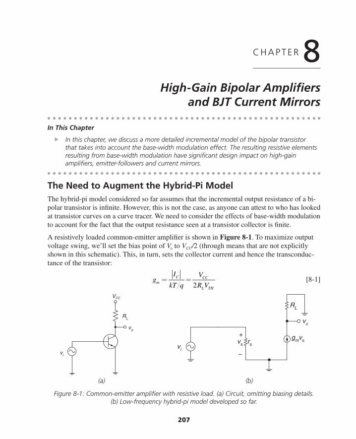
207
C H A P T E R 8High-Gain Bipolar Amplifi ers
and BJT Current Mirrors
The Need to Augment the Hybrid-Pi ModelThe hybrid-pi model considered so far assumes that the incremental output resistance of a bi-polar transistor is infi nite. However, this is not the case, as anyone can attest to who has looked at transistor curves on a curve tracer. We need to consider the effects of base-width modulation to account for the fact that the output resistance seen at a transistor collector is fi nite.
A resistively loaded common-emitter amplifi er is shown in Figure 8-1. To maximize output voltage swing, we’ll set the bias point of Vo to VCC/2 (through means that are not explicitly shown in this schematic). This, in turn, sets the collector current and hence the transconduc-tance of the transistor:
2
C CCm
L TH
I Vg
kT q R V= = [8-1]
In This Chapter
In this chapter, we discuss a more detailed incremental model of the bipolar transistor that takes into account the base-width modulation effect. The resulting resistive elements resulting from base-width modulation have signifi cant design impact on high-gain amplifi ers, emitter-followers and current mirrors.
(a) (b)
Figure 8-1: Common-emitter amplifi er with resistive load. (a) Circuit, omitting biasing details. (b) Low-frequency hybrid-pi model developed so far.
vi
vo
RL
+
–
rπgmvπvπ
vo
RL
vi
VCC
Thompson Book.indb 207 3/20/2006 11:35:22 AM
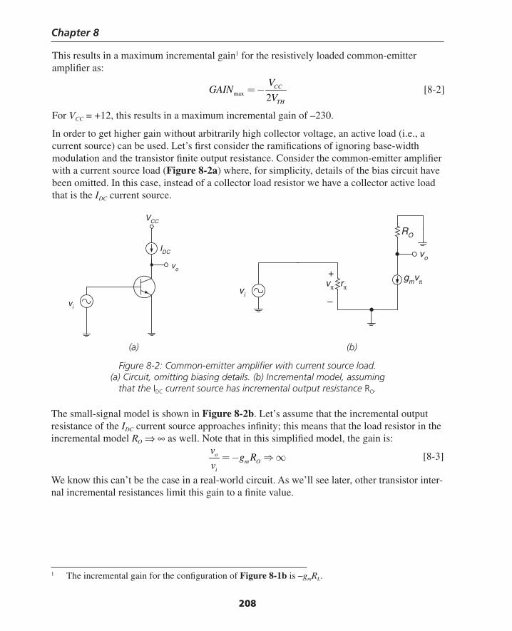
Chapter 8
208
This results in a maximum incremental gain1 for the resistively loaded common-emitter amplifi er as:
max 2CC
TH
VGAIN
V= − [8-2]
For VCC = +12, this results in a maximum incremental gain of –230.
In order to get higher gain without arbitrarily high collector voltage, an active load (i.e., a current source) can be used. Let’s fi rst consider the ramifi cations of ignoring base-width modulation and the transistor fi nite output resistance. Consider the common-emitter amplifi er with a current source load (Figure 8-2a) where, for simplicity, details of the bias circuit have been omitted. In this case, instead of a collector load resistor we have a collector active load that is the IDC current source.
1 The incremental gain for the confi guration of Figure 8-1b is –gmRL.
(a) (b)
Figure 8-2: Common-emitter amplifi er with current source load. (a) Circuit, omitting biasing details. (b) Incremental model, assuming
that the IDC current source has incremental output resistance RO.
The small-signal model is shown in Figure 8-2b. Let’s assume that the incremental output resistance of the IDC current source approaches infi nity; this means that the load resistor in the incremental model RO ⇒ ∞ as well. Note that in this simplifi ed model, the gain is:
om O
i
vg R
v= − ⇒ ∞ [8-3]
We know this can’t be the case in a real-world circuit. As we’ll see later, other transistor inter-nal incremental resistances limit this gain to a fi nite value.
vi
vo
VCC
IDC
+
–
rπgmvπvπ
vo
RO
vi
Thompson Book.indb 208 3/20/2006 11:35:22 AM
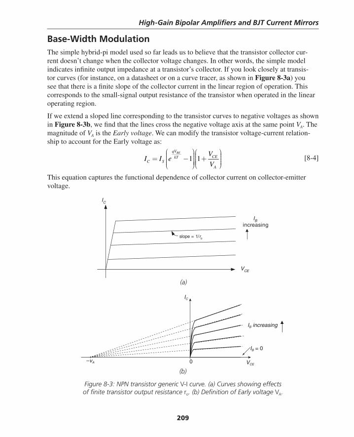
High-Gain Bipolar Amplifi ers and BJT Current Mirrors
209
Base-Width ModulationThe simple hybrid-pi model used so far leads us to believe that the transistor collector cur-rent doesn’t change when the collector voltage changes. In other words, the simple model indicates infi nite output impedance at a transistor’s collector. If you look closely at transis-tor curves (for instance, on a datasheet or on a curve tracer, as shown in Figure 8-3a) you see that there is a fi nite slope of the collector current in the linear region of operation. This corresponds to the small-signal output resistance of the transistor when operated in the linear operating region.
If we extend a sloped line corresponding to the transistor curves to negative voltages as shown in Figure 8-3b, we fi nd that the lines cross the negative voltage axis at the same point VA. The magnitude of VA is the Early voltage. We can modify the transistor voltage-current relation-ship to account for the Early voltage as:
1 1BEqV
CEkTC S
A
VI I e
V
⎛ ⎞⎛ ⎞⎟ ⎟⎜ ⎜⎟ ⎟= − +⎜ ⎜⎟ ⎟⎜ ⎜⎟ ⎟⎜⎟⎜ ⎝ ⎠⎝ ⎠ [8-4]
This equation captures the functional dependence of collector current on collector-emitter voltage.
(a)
VCE
IC
slope = 1/ro
IBincreasing
IC
IB increasing
IB = 0
VCE–vA 0
(b)
Figure 8-3: NPN transistor generic V-I curve. (a) Curves showing effects of fi nite transistor output resistance ro. (b) Defi nition of Early voltage VA.
Thompson Book.indb 209 3/20/2006 11:35:23 AM
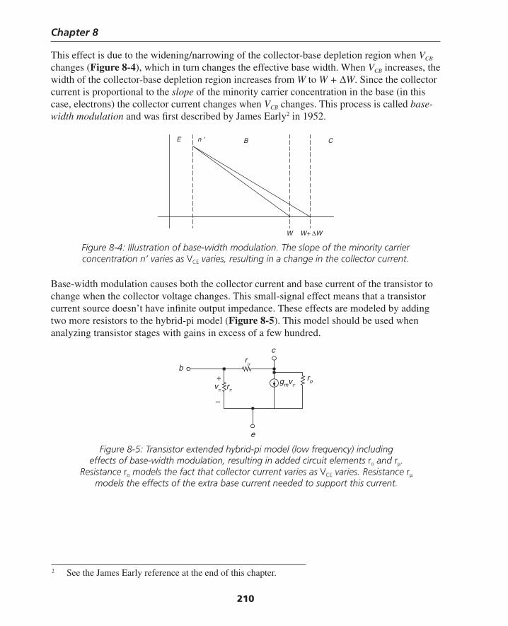
Chapter 8
210
This effect is due to the widening/narrowing of the collector-base depletion region when VCB changes (Figure 8-4), which in turn changes the effective base width. When VCB increases, the width of the collector-base depletion region increases from W to W + ΔW. Since the collector current is proportional to the slope of the minority carrier concentration in the base (in this case, electrons) the collector current changes when VCB changes. This process is called base-width modulation and was fi rst described by James Early2 in 1952.
2 See the James Early reference at the end of this chapter.
Figure 8-4: Illustration of base-width modulation. The slope of the minority carrier concentration n’ varies as VCE varies, resulting in a change in the collector current.
Base-width modulation causes both the collector current and base current of the transistor to change when the collector voltage changes. This small-signal effect means that a transistor current source doesn’t have infi nite output impedance. These effects are modeled by adding two more resistors to the hybrid-pi model (Figure 8-5). This model should be used when analyzing transistor stages with gains in excess of a few hundred.
B CE n '
W W+ ΔW
+
–
b
rπ
e
gmvπvπ
crμ
ro
Figure 8-5: Transistor extended hybrid-pi model (low frequency) including effects of base-width modulation, resulting in added circuit elements ro and rμ.
Resistance ro models the fact that collector current varies as VCE varies. Resistance rμ models the effects of the extra base current needed to support this current.
Thompson Book.indb 210 3/20/2006 11:35:23 AM
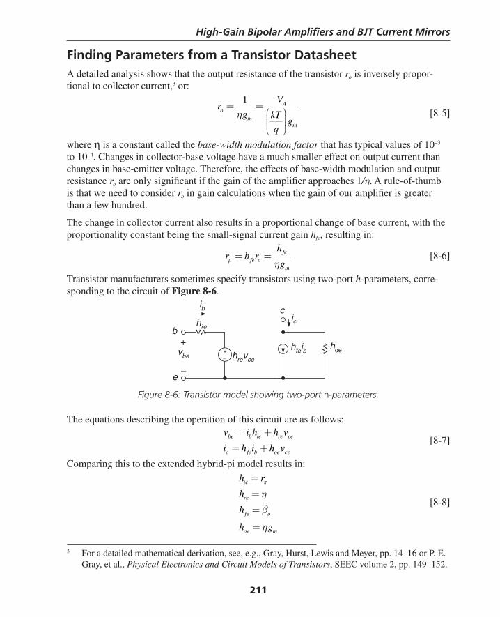
High-Gain Bipolar Amplifi ers and BJT Current Mirrors
211
Finding Parameters from a Transistor DatasheetA detailed analysis shows that the output resistance of the transistor ro is inversely propor-tional to collector current,3 or:
1 A
om
m
Vr
g kTg
q
η= =
⎛ ⎞⎟⎜ ⎟⎜ ⎟⎜ ⎟⎝ ⎠
[8-5]
where η is a constant called the base-width modulation factor that has typical values of 10–3 to 10–4. Changes in collector-base voltage have a much smaller effect on output current than changes in base-emitter voltage. Therefore, the effects of base-width modulation and output resistance ro are only signifi cant if the gain of the amplifi er approaches 1/η. A rule-of-thumb is that we need to consider ro in gain calculations when the gain of our amplifi er is greater than a few hundred.
The change in collector current also results in a proportional change of base current, with the proportionality constant being the small-signal current gain hfe, resulting in:
fefe o
m
hr h r
gμ η= = [8-6]
Transistor manufacturers sometimes specify transistors using two-port h-parameters, corre-sponding to the circuit of Figure 8-6.
3 For a detailed mathematical derivation, see, e.g., Gray, Hurst, Lewis and Meyer, pp. 14–16 or P. E. Gray, et al., Physical Electronics and Circuit Models of Transistors, SEEC volume 2, pp. 149–152.
b
e
hfeib
c
+–
hie
hrevce
hoe
ibic
vbe
+
–
Figure 8-6: Transistor model showing two-port h-parameters.
The equations describing the operation of this circuit are as follows:
be b ie re ce
c fe b oe ce
v i h h v
i h i h v
= +
= + [8-7]
Comparing this to the extended hybrid-pi model results in:
ie
re
fe o
oe m
h r
h
h
h g
π
η
β
η
=
=
=
=
[8-8]
Thompson Book.indb 211 3/20/2006 11:35:24 AM
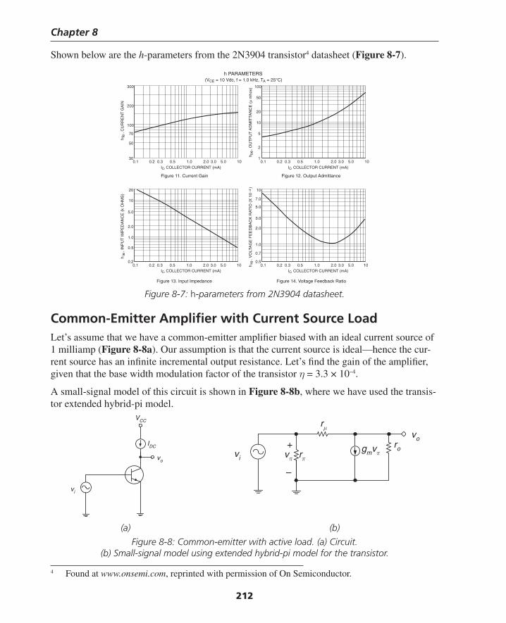
Chapter 8
212
Shown below are the h-parameters from the 2N3904 transistor4 datasheet (Figure 8-7).
4 Found at www.onsemi.com, reprinted with permission of On Semiconductor.
Figure 8-7: h-parameters from 2N3904 datasheet.
Common-Emitter Amplifi er with Current Source LoadLet’s assume that we have a common-emitter amplifi er biased with an ideal current source of 1 milliamp (Figure 8-8a). Our assumption is that the current source is ideal—hence the cur-rent source has an infi nite incremental output resistance. Let’s fi nd the gain of the amplifi er, given that the base width modulation factor of the transistor η = 3.3 × 10⁻⁴.
A small-signal model of this circuit is shown in Figure 8-8b, where we have used the transis-tor extended hybrid-pi model.
Figure 11. Current Gain
IC, COLLECTOR CURRENT (mA)
70
100
200
300
50
Figure 12. Output Admittance
IC, COLLECTOR CURRENT (mA)
h
, CU
RR
EN
T G
AIN
h
, OU
TP
UT
AD
MIT
TAN
CE
(
mho
s)
Figure 13. Input Impedance
IC, COLLECTOR CURRENT (mA)
Figure 14. Voltage Feedback Ratio
IC, COLLECTOR CURRENT (mA)
30
100
50
5
10
20
2.0
3.0
5.0
7.0
10
1.0
0.1 0.2 1.0 2.0 5.00.5
100.3 0.5 3.0
0.7
2.0
5.0
10
20
1.0
0.2
0.5oe
h
, VO
LTA
GE
FE
ED
BA
CK
RA
TIO
(X
10
)
re
h
, IN
PU
T IM
PE
DA
NC
E (
k O
HM
S)
ie
0.1 0.2 1.0 2.0 5.0 100.3 0.5 3.0
0.1 0.2 1.0 2.0 5.0 100.3 0.5 3.0
2
10.1 0.2 1.0 2.0 5.0 100.3 0.5 3.0
fe
−4
h PARAMETERS(VCE = 10 Vdc, f = 1.0 kHz, TA = 25°C)
vi
vo
VCC
IDC +
–
rπgmvπvπ
vo
rμ
rovi
(a) (b)
Figure 8-8: Common-emitter with active load. (a) Circuit. (b) Small-signal model using extended hybrid-pi model for the transistor.
Thompson Book.indb 212 3/20/2006 11:35:25 AM
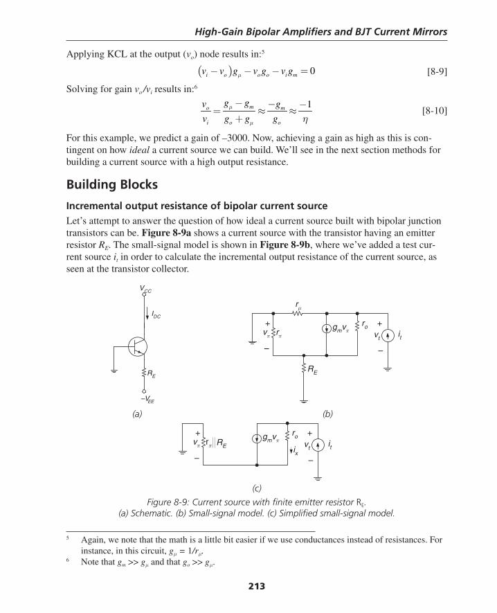
High-Gain Bipolar Amplifi ers and BJT Current Mirrors
213
Applying KCL at the output (vo) node results in:5
( ) 0i o o o i mv v g v g v gμ− − − = [8-9]
Solving for gain vo /vi results in:6
1mo m
i o o
g gv g
v g g gμ
μ η
− − −= ≈ ≈
+ [8-10]
For this example, we predict a gain of –3000. Now, achieving a gain as high as this is con-tingent on how ideal a current source we can build. We’ll see in the next section methods for building a current source with a high output resistance.
Building Blocks
Incremental output resistance of bipolar current sourceLet’s attempt to answer the question of how ideal a current source built with bipolar junction transistors can be. Figure 8-9a shows a current source with the transistor having an emitter resistor RE. The small-signal model is shown in Figure 8-9b, where we’ve added a test cur-rent source it in order to calculate the incremental output resistance of the current source, as seen at the transistor collector.
5 Again, we note that the math is a little bit easier if we use conductances instead of resistances. For instance, in this circuit, gμ = 1/rμ.
6 Note that gm >> gμ and that go >> gμ.
(a) (b)
IDC
–VEE
VCC
RE
+
–
rπgmvπvπ
rμ
ro
RE
it
+
–
vt
+
–
rπgmvπvπ
roit
+
–
vtRE ix
(c)
Figure 8-9: Current source with fi nite emitter resistor RE. (a) Schematic. (b) Small-signal model. (c) Simplifi ed small-signal model.
Thompson Book.indb 213 3/20/2006 11:35:25 AM
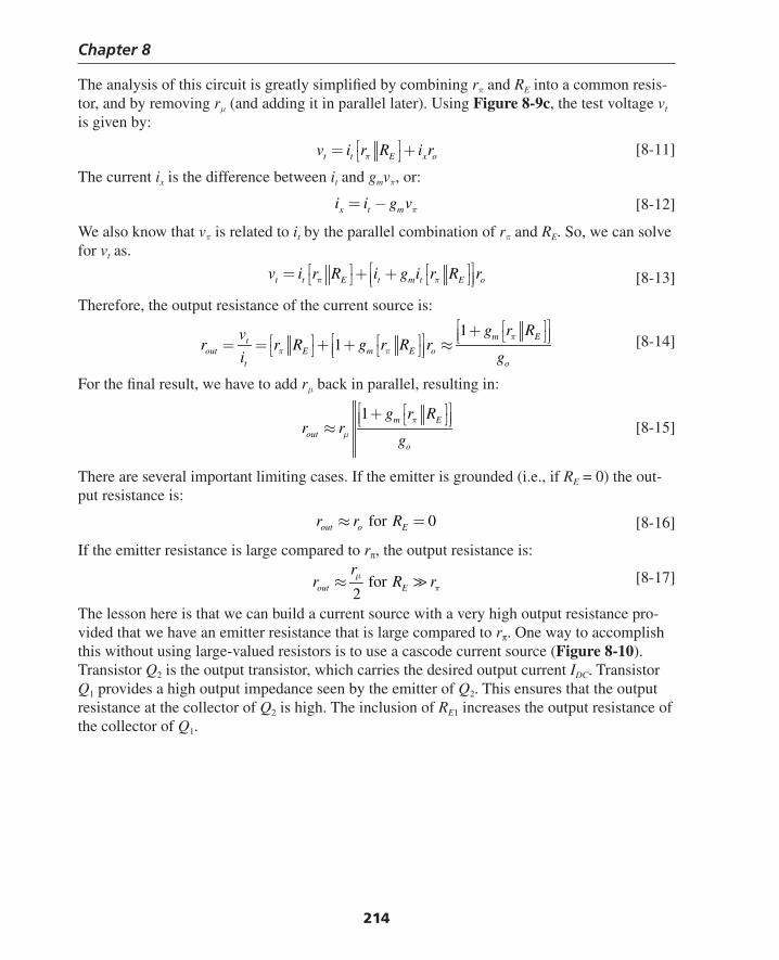
Chapter 8
214
The analysis of this circuit is greatly simplifi ed by combining rπ and RE into a common resis-tor, and by removing rμ (and adding it in parallel later). Using Figure 8-9c, the test voltage vt is given by:
t t E x ov i r R i rπ⎡ ⎤= +⎣ ⎦ [8-11]
The current ix is the difference between it and gmvπ, or:
x t mi i g vπ= − [8-12]
We also know that vπ is related to it by the parallel combination of rπ and RE. So, we can solve for vt as.
t t E t m t E ov i r R i g i r R rπ π⎡ ⎤⎡ ⎤ ⎡ ⎤= + +⎢ ⎥⎣ ⎦ ⎣ ⎦⎣ ⎦ [8-13]
Therefore, the output resistance of the current source is:
1
1m Et
out E m E ot o
g r Rvr r R g r R r
i g
π
π π
⎡ ⎤⎡ ⎤+⎢ ⎥⎣ ⎦⎣ ⎦⎡ ⎤⎡ ⎤ ⎡ ⎤= = + + ≈⎢ ⎥⎣ ⎦ ⎣ ⎦⎣ ⎦ [8-14]
For the fi nal result, we have to add rμ back in parallel, resulting in:
1 m E
outo
g r Rr r
g
π
μ
⎡ ⎤⎡ ⎤+⎢ ⎥⎣ ⎦⎣ ⎦≈ [8-15]
There are several important limiting cases. If the emitter is grounded (i.e., if RE = 0) the out-put resistance is:
for 0out o Er r R≈ = [8-16]
If the emitter resistance is large compared to rπ, the output resistance is:
for2out E
rr R rμ
π≈ [8-17]
The lesson here is that we can build a current source with a very high output resistance pro-vided that we have an emitter resistance that is large compared to rπ. One way to accomplish this without using large-valued resistors is to use a cascode current source (Figure 8-10). Transistor Q2 is the output transistor, which carries the desired output current IDC. Transistor Q1 provides a high output impedance seen by the emitter of Q2. This ensures that the output resistance at the collector of Q2 is high. The inclusion of RE1 increases the output resistance of the collector of Q1.
Thompson Book.indb 214 3/20/2006 11:35:25 AM
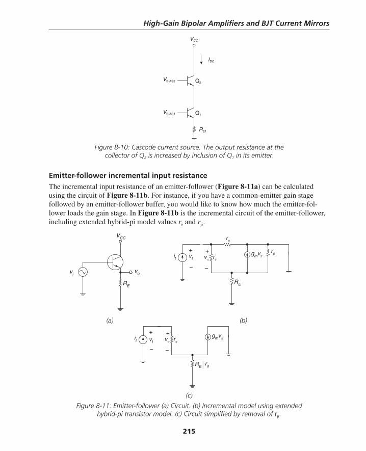
High-Gain Bipolar Amplifi ers and BJT Current Mirrors
215
VCC
vivo
RE
+
–
rπgmvπvπ
rμ
ro
RE
+
–
vtit
+
–
rπgmvπvπ
roRE
it+
–
vt
Figure 8-10: Cascode current source. The output resistance at the collector of Q2 is increased by inclusion of Q1 in its emitter.
Emitter-follower incremental input resistanceThe incremental input resistance of an emitter-follower (Figure 8-11a) can be calculated using the circuit of Figure 8-11b. For instance, if you have a common-emitter gain stage followed by an emitter-follower buffer, you would like to know how much the emitter-fol-lower loads the gain stage. In Figure 8-11b is the incremental circuit of the emitter-follower, including extended hybrid-pi model values ro and rμ.
Q2
Q1
VCC
IDC
RE1
VBIAS1
VBIAS2
(a) (b)
(c)
Figure 8-11: Emitter-follower (a) Circuit. (b) Incremental model using extended hybrid-pi transistor model. (c) Circuit simplifi ed by removal of rμ.
Thompson Book.indb 215 3/20/2006 11:35:26 AM
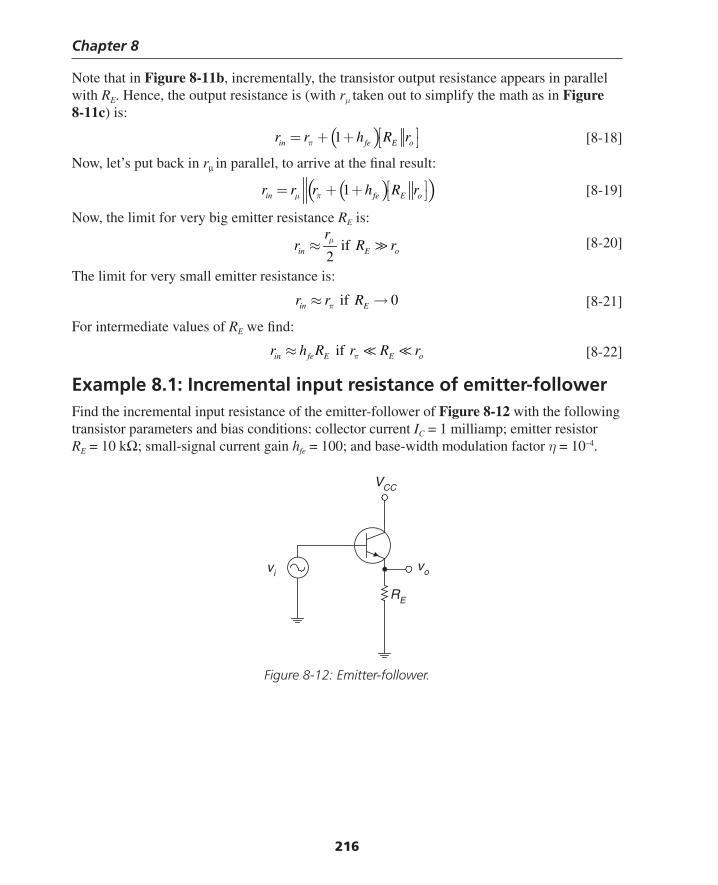
Chapter 8
216
Note that in Figure 8-11b, incrementally, the transistor output resistance appears in parallel with RE. Hence, the output resistance is (with rμ taken out to simplify the math as in Figure 8-11c) is:
( )1in fe E or r h R rπ⎡ ⎤= + + ⎣ ⎦ [8-18]
Now, let’s put back in rμ in parallel, to arrive at the fi nal result:
( )( )1in fe E or r r h R rμ π⎡ ⎤= + + ⎣ ⎦ [8-19]
Now, the limit for very big emitter resistance RE is:
if2in E o
rr R rμ≈ [8-20]
The limit for very small emitter resistance is:
if 0in Er r Rπ≈ → [8-21]
For intermediate values of RE we fi nd:
ifin fe E E or h R r R rπ≈ [8-22]
Example 8.1: Incremental input resistance of emitter-followerFind the incremental input resistance of the emitter-follower of Figure 8-12 with the following transistor parameters and bias conditions: collector current IC = 1 milliamp; emitter resistor RE = 10 kΩ; small-signal current gain hfe = 100; and base-width modulation factor η = 10–4.
Figure 8-12: Emitter-follower.
VCC
vivo
RE
Thompson Book.indb 216 3/20/2006 11:35:27 AM
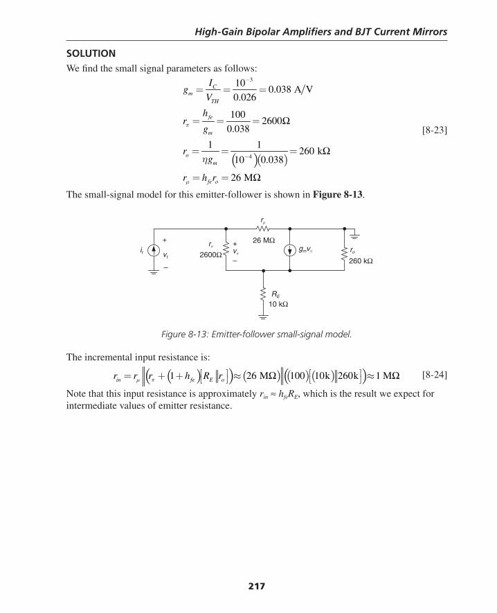
High-Gain Bipolar Amplifi ers and BJT Current Mirrors
217
SOLUTIONWe fi nd the small signal parameters as follows:
( )( )
3
4
100.038 A V
0.026
1002600
0.038
1 1260 k
10 0.038
26 M
Cm
TH
fe
m
om
fe o
Ig
V
hr
g
rg
r h r
π
μ
η
−
−
= = =
= = =
= = =
= =
Ω
Ω
Ω
[8-23]
The small-signal model for this emitter-follower is shown in Figure 8-13.
Figure 8-13: Emitter-follower small-signal model.
The incremental input resistance is:
( )( ) ( ) ( )( )( )1 26 M 100 10k 260k 1 Min fe E or r r h R rμ π⎡ ⎤⎡ ⎤= + + ≈ ≈⎣ ⎦ ⎣ ⎦Ω Ω [8-24]
Note that this input resistance is approximately rin ≈ hfeRE, which is the result we expect for intermediate values of emitter resistance.
+
–
RE
2600Ωit vt
ro
rπvπ
gmvπ
–
+ 26 MΩ
rμ
260 kΩ
10 kΩ
Thompson Book.indb 217 3/20/2006 11:35:27 AM
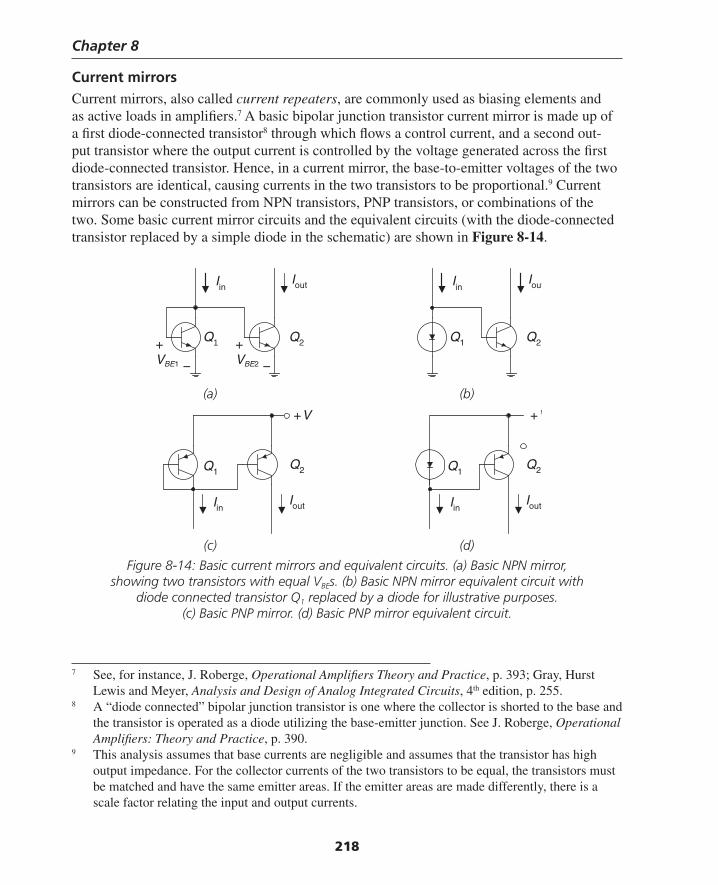
Chapter 8
218
Current mirrorsCurrent mirrors, also called current repeaters, are commonly used as biasing elements and as active loads in amplifi ers.7 A basic bipolar junction transistor current mirror is made up of a fi rst diode-connected transistor8 through which fl ows a control current, and a second out-put transistor where the output current is controlled by the voltage generated across the fi rst diode-connected transistor. Hence, in a current mirror, the base-to-emitter voltages of the two transistors are identical, causing currents in the two transistors to be proportional.9 Current mirrors can be constructed from NPN transistors, PNP transistors, or combinations of the two. Some basic current mirror circuits and the equivalent circuits (with the diode-connected transistor replaced by a simple diode in the schematic) are shown in Figure 8-14.
7 See, for instance, J. Roberge, Operational Amplifi ers Theory and Practice, p. 393; Gray, Hurst Lewis and Meyer, Analysis and Design of Analog Integrated Circuits, 4th edition, p. 255.
8 A “diode connected” bipolar junction transistor is one where the collector is shorted to the base and the transistor is operated as a diode utilizing the base-emitter junction. See J. Roberge, Operational Amplifi ers: Theory and Practice, p. 390.
9 This analysis assumes that base currents are negligible and assumes that the transistor has high output impedance. For the collector currents of the two transistors to be equal, the transistors must be matched and have the same emitter areas. If the emitter areas are made differently, there is a scale factor relating the input and output currents.
Q1 Q2
Iin Iout
Q1 Q2
Iin Iout
Q1Q2
Iin Iout
+V
Q1Q2
Iin Iout
+V
VBE1
+
− VBE2
+
−
(c) (d)
Figure 8-14: Basic current mirrors and equivalent circuits. (a) Basic NPN mirror, showing two transistors with equal VBEs. (b) Basic NPN mirror equivalent circuit with
diode connected transistor Q1 replaced by a diode for illustrative purposes. (c) Basic PNP mirror. (d) Basic PNP mirror equivalent circuit.
(a) (b)
Thompson Book.indb 218 3/20/2006 11:35:28 AM
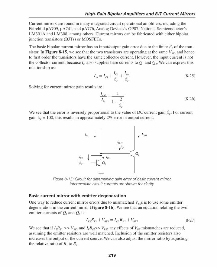
High-Gain Bipolar Amplifi ers and BJT Current Mirrors
219
Q2
Q1
IOUTIIN
IOUT
βF
IC1
βF
IC1
Current mirrors are found in many integrated circuit operational amplifi ers, including the Fairchild µA709, µA741, and µA776, Analog Devices’s OP07, National Semiconductor’s LM301A and LM308, among others. Current mirrors can be fabricated with either bipolar junction transistors (BJTs) or MOSFETs.
The basic bipolar current mirror has an input/output gain error due to the fi nite βF of the tran-sistor. In Figure 8-15, we see that the two transistors are operating at the same VBE, and hence to fi rst order the transistors have the same collector current. However, the input current is not the collector current, because Iin also supplies base currents to Q1 and Q2. We can express this relationship as:
11
C outin C
F F
I II I
β β= + + [8-25]
Solving for current mirror gain results in:
1
21
out
in
F
I
Iβ
=+
[8-26]
We see that the error is inversely proportional to the value of DC current gain βF. For current gain βF = 100, this results in approximately 2% error in output current.
Figure 8-15: Circuit for determining gain error of basic current mirror. Intermediate circuit currents are shown for clarity.
Basic current mirror with emitter degenerationOne way to reduce current mirror errors due to mismatched VBEs is to use some emitter degeneration in the current mirror (Figure 8-16). We see that an equation relating the two emitter currents of Q1 and Q2 is:
1 1 1 2 2 2E E BE E E BEI R V I R V+ = + [8-27]
We see that if IERE1 >> VBE1 and IERE2>> VBE2 any effects of VBE mismatches are reduced, assuming the emitter resistors are well matched. Inclusion of the emitter resistors also increases the output of the current source. We can also adjust the mirror ratio by adjusting the relative ratio of R1 to R2.
Thompson Book.indb 219 3/20/2006 11:35:28 AM
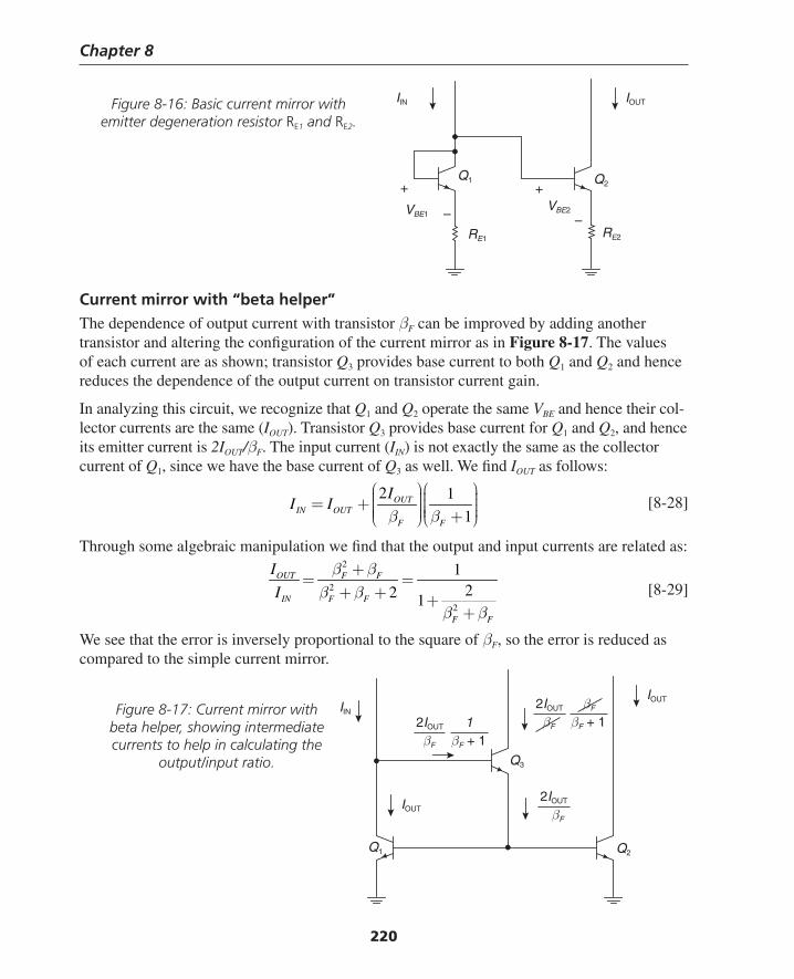
Chapter 8
220
Current mirror with “beta helper”The dependence of output current with transistor βF can be improved by adding another transistor and altering the confi guration of the current mirror as in Figure 8-17. The values of each current are as shown; transistor Q3 provides base current to both Q1 and Q2 and hence reduces the dependence of the output current on transistor current gain.
In analyzing this circuit, we recognize that Q1 and Q2 operate the same VBE and hence their col-lector currents are the same (IOUT). Transistor Q3 provides base current for Q1 and Q2, and hence its emitter current is 2IOUT/βF. The input current (IIN) is not exactly the same as the collector current of Q1, since we have the base current of Q3 as well. We fi nd IOUT as follows:
2 1
1OUT
IN OUTF F
II I
β β
⎛ ⎞⎛ ⎞⎟ ⎟⎜ ⎜⎟ ⎟= +⎜ ⎜⎟ ⎟⎜ ⎜⎟ ⎟⎜ ⎜ +⎝ ⎠⎝ ⎠ [8-28]
Through some algebraic manipulation we fi nd that the output and input currents are related as:
2
2
2
122 1
OUT F F
IN F F
F F
I
I
β ββ β
β β
+= =
+ + ++
[8-29]
We see that the error is inversely proportional to the square of βF, so the error is reduced as compared to the simple current mirror.
Q2Q1
IOUTIIN
VBE1VBE2
RE2RE1
+ +
––
Q2
IOUT
IIN
Q3
Q1
IOUT
2IOUT
βF
2IOUT
βF
1βF + 1
2IOUT
βF
βF
βF + 1
Figure 8-16: Basic current mirror with emitter degeneration resistor RE1 and RE2.
Figure 8-17: Current mirror with beta helper, showing intermediate currents to help in calculating the
output/input ratio.
Thompson Book.indb 220 3/20/2006 11:35:29 AM
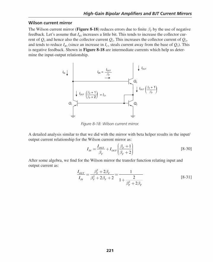
High-Gain Bipolar Amplifi ers and BJT Current Mirrors
221
Wilson current mirrorThe Wilson current mirror (Figure 8-18) reduces errors due to fi nite βF by the use of negative feedback. Let’s assume that IB3 increases a little bit. This tends to increase the collector cur-rent of Q3 and hence also the collector current Q2. This increases the collector current of Q2, and tends to reduce IB3 (since an increase in IC1 steals current away from the base of Q3). This is negative feedback. Shown in Figure 8-18 are intermediate currents which help us deter-mine the input-output relationship.
Q2
IOUT
IIN
Q3
Q1
IOUT
βF + 1βFβF + 1
βF + 2
IOUT ⎛⎜⎝ ⎛⎜⎝⎛⎜⎝ ⎛⎜⎝
IOUT
βF
IB3 =
= IC1
Figure 8-18: Wilson current mirror.
A detailed analysis similar to that we did with the mirror with beta helper results in the input/output current relationship for the Wilson current mirror as:
1
2OUT F
IN OUTF F
II I
ββ β
⎛ ⎞+ ⎟⎜ ⎟= + ⎜ ⎟⎜ ⎟⎜ +⎝ ⎠ [8-30]
After some algebra, we fi nd for the Wilson mirror the transfer function relating input and output current as:
2
2
2
2 122 2 1
2
OUT F F
IN F F
F F
I
I
β ββ β
β β
+= =
+ + ++
[8-31]
Thompson Book.indb 221 3/20/2006 11:35:29 AM
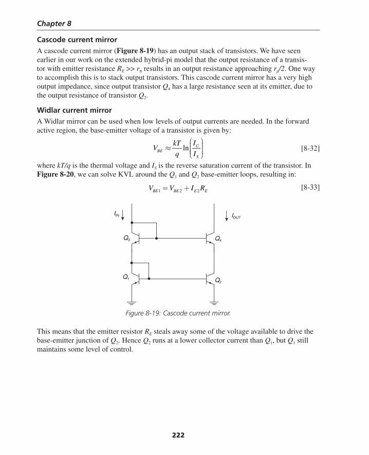
Chapter 8
222
Cascode current mirrorA cascode current mirror (Figure 8-19) has an output stack of transistors. We have seen earlier in our work on the extended hybrid-pi model that the output resistance of a transis-tor with emitter resistance RE >> rπ results in an output resistance approaching rµ/2. One way to accomplish this is to stack output transistors. This cascode current mirror has a very high output impedance, since output transistor Q4 has a large resistance seen at its emitter, due to the output resistance of transistor Q2.
Widlar current mirrorA Widlar mirror can be used when low levels of output currents are needed. In the forward active region, the base-emitter voltage of a transistor is given by:
ln CBE
S
IkTV
q I
⎛ ⎞⎟⎜ ⎟≈ ⎜ ⎟⎜ ⎟⎜⎝ ⎠ [8-32]
where kT/q is the thermal voltage and IS is the reverse saturation current of the transistor. In Figure 8-20, we can solve KVL around the Q1 and Q2 base-emitter loops, resulting in:
1 2 2BE BE E EV V I R= + [8-33]
Q2
IIN
Q1
IOUT
Q4Q3
Figure 8-19: Cascode current mirror.
This means that the emitter resistor RE steals away some of the voltage available to drive the base-emitter junction of Q2. Hence Q2 runs at a lower collector current than Q1, but Q1 still maintains some level of control.
Thompson Book.indb 222 3/20/2006 11:35:30 AM
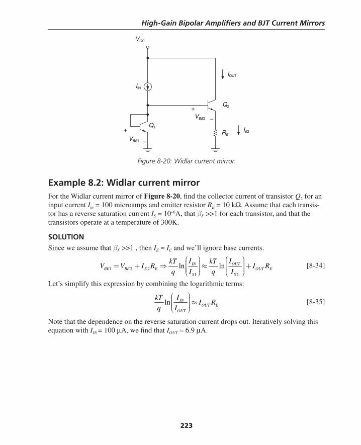
High-Gain Bipolar Amplifi ers and BJT Current Mirrors
223
Figure 8-20: Widlar current mirror.
Example 8.2: Widlar current mirrorFor the Widlar current mirror of Figure 8-20, fi nd the collector current of transistor Q2 for an input current Iin = 100 microamps and emitter resistor RE = 10 kΩ. Assume that each transis-tor has a reverse saturation current IS = 10–6A, that βF >>1 for each transistor, and that the transistors operate at a temperature of 300K.
SOLUTIONSince we assume that βF >>1 , then IE ≈ IC and we’ll ignore base currents.
1 2 21 2
ln lnIN OUTBE BE E E OUT E
S S
I IkT kTV V I R I R
q I q I
⎛ ⎞ ⎛ ⎞⎟ ⎟⎜ ⎜⎟ ⎟= + ⇒ ≈ +⎜ ⎜⎟ ⎟⎜ ⎜⎟ ⎟⎜ ⎜⎝ ⎠ ⎝ ⎠ [8-34]
Let’s simplify this expression by combining the logarithmic terms:
ln INOUT E
OUT
IkTI R
q I
⎛ ⎞⎟⎜ ⎟ ≈⎜ ⎟⎜ ⎟⎜⎝ ⎠ [8-35]
Note that the dependence on the reverse saturation current drops out. Iteratively solving this equation with IIN = 100 μA, we fi nd that IOUT ≈ 6.9 μA.
Q2
IIN
Q1
IOUT
IE2
VCC
VBE1
VBE2
+
–
–
RE+
Thompson Book.indb 223 3/20/2006 11:35:30 AM
Chapter 8
224
Example 8.3: Widlar mirror incremental output resistanceFor the Widlar current mirror of Figure 8-20, fi nd the incremental output resistance measured at the collector of Q2. Again, assume that RE = 10 kΩ. For Q2, assume the following param-eters: hfe = 100; η = 3.3 × 10⁻⁴.
SOLUTIONWe fi nd the small-signal parameters as follows:
( )( )
642
4
4 4
6.9 102.65 10 A V
0.026
100377 k
2.65 10
1 111.4 M
3.3 10 2.65 10
1140 M
Cm
TH
fe
m
om
fe o
Ig
V
hr
g
rg
r h r
π
μ
η
−−
−
− −
×= = = ×
= = =×
= = =× ×
= =
Ω
Ω
Ω
[8-36]
The full expression for the output resistance of transistor Q2 with emitter degeneration is:
1 m E
outo
g r Rr r
g
π
μ
⎡ ⎤⎡ ⎤+⎢ ⎥⎣ ⎦⎣ ⎦≈ [8-37]
Note that in this case RE << rπ and hence we can approximate the output resistance as:
( )( )( )42.65 10 10,000 11.4 M 30.2 Mout m E or g R r −≈ ≈ × ≈Ω Ω [8-38]
Example 8.4: Current mirror error due to mismatched VCEsA circuit illustrating the cause of current mirror mismatch due to the Early effect is shown in Figure 8-21. Transistor Q1 is an input diode-connected transistor biased by a 10-milliamp current source (I1). The SPICE plot10 of Figure 8-21b shows the collector current of transistor Q2 as the power supply voltage is varied from 0 to 20 volts. In this case, the VCE of Q1 fi xed at a VBE drop (due to the diode connection) while the VCE of Q2 is signifi cantly higher. The col-lector current of Q2 varies signifi cantly over the range of power supply voltages. The collector current of Q2 rises to ∼10 milliamps when the supply voltage reaches ∼0.5 volts. This is when transistor Q2 leaves saturation and enters the forward-active region.
10 The schematic of Figure 8-21a shows the node voltages for a power supply voltage of +12V.
Thompson Book.indb 224 3/20/2006 11:35:31 AM
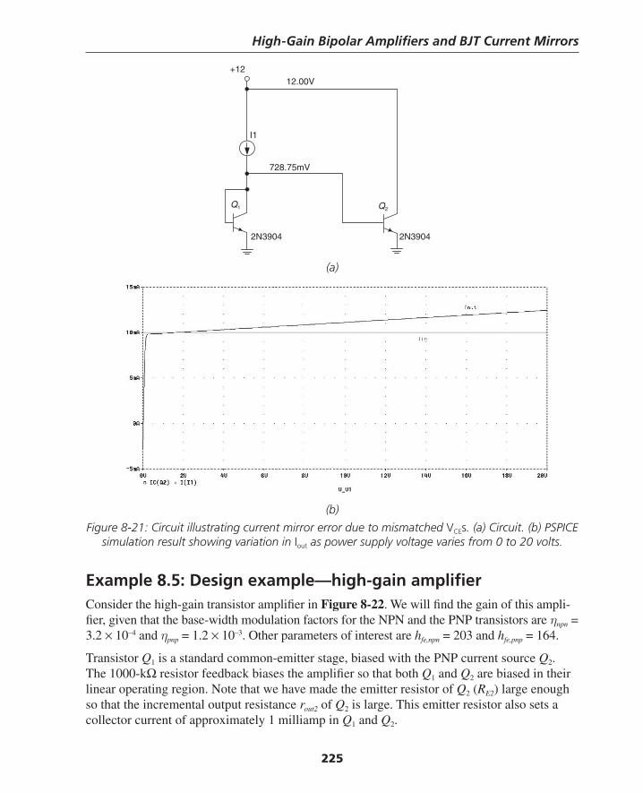
High-Gain Bipolar Amplifi ers and BJT Current Mirrors
225
(a)
2N3904 2N3904
Q1
+12
I1
Q2
12.00V
728.75mV
(b)
Figure 8-21: Circuit illustrating current mirror error due to mismatched VCEs. (a) Circuit. (b) PSPICE simulation result showing variation in Iout as power supply voltage varies from 0 to 20 volts.
Example 8.5: Design example—high-gain amplifi erConsider the high-gain transistor amplifi er in Figure 8-22. We will fi nd the gain of this ampli-fi er, given that the base-width modulation factors for the NPN and the PNP transistors are ηnpn = 3.2 × 10⁻⁴ and ηpnp = 1.2 × 10⁻³. Other parameters of interest are hfe,npn = 203 and hfe,pnp = 164.
Transistor Q1 is a standard common-emitter stage, biased with the PNP current source Q2. The 1000-kΩ resistor feedback biases the amplifi er so that both Q1 and Q2 are biased in their linear operating region. Note that we have made the emitter resistor of Q2 (RE2) large enough so that the incremental output resistance rout2 of Q2 is large. This emitter resistor also sets a collector current of approximately 1 milliamp in Q1 and Q2.
Thompson Book.indb 225 3/20/2006 11:35:31 AM
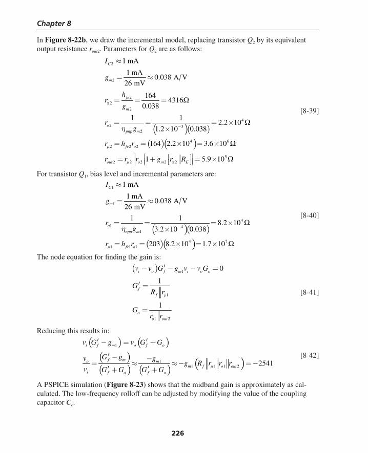
Chapter 8
226
In Figure 8-22b, we draw the incremental model, replacing transistor Q2 by its equivalent output resistance rout2. Parameters for Q2 are as follows:
( )( )
( )( )
2
2
22
2
42 3
2
4 62 2 2
52 2 2 2 2
1 mA
1 mA0.038 A V
26 mV
1644316
0.038
1 12.2 10
1.2 10 0.038
164 2.2 10 3.6 10
1 5.9 10
C
m
fe
m
opnp m
fe o
out o m E
I
g
hr
g
rg
r h r
r r r g r R
π
μ
μ π
η −
≈
= ≈
= = =
= = = ××
= = × = ×
⎡ ⎤⎡ ⎤= + = ×⎢ ⎥⎣ ⎦⎣ ⎦
Ω
Ω
Ω
Ω
[8-39]
For transistor Q1, bias level and incremental parameters are:
( )( )
( )( )
1
1
41 4
1
4 71 1 1
1 mA
1 mA0.038 A V
26 mV
1 18.2 10
3.2 10 0.038
203 8.2 10 1.7 10
C
m
onpn m
fe o
I
g
rg
r h rμ
η −
≈
= ≈
= = = ××
= = × = ×
Ω
Ω
[8-40]
The node equation for fi nding the gain is:
( ) 1
1
1 2
0
1
1
i o f m i o o
f
f
oo out
v v G g v v G
GR r
Gr r
μ
′− − − =
′ =
=
[8-41]
Reducing this results in:
( ) ( )( )( ) ( ) ( )
1
11 1 1 2 2541
i f m o f o
f mo mm f o out
i f o f o
v G g v G G
G gv gg R r r r
v G G G Gμ
′ ′− = +
′ − −= ≈ ≈ − = −
′ ′+ +
[8-42]
A PSPICE simulation (Figure 8-23) shows that the midband gain is approximately as cal-culated. The low-frequency rolloff can be adjusted by modifying the value of the coupling capacitor Cc.
Thompson Book.indb 226 3/20/2006 11:35:32 AM
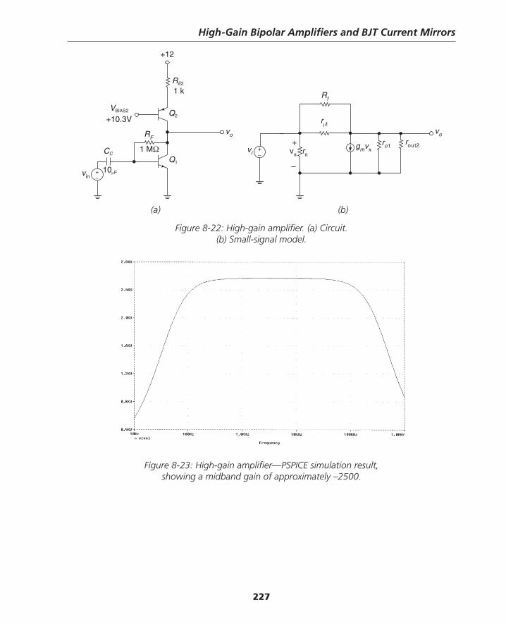
High-Gain Bipolar Amplifi ers and BJT Current Mirrors
227
(a) (b)
Figure 8-22: High-gain amplifi er. (a) Circuit. (b) Small-signal model.
+
–
rπgmvπvπ
rμ1
ro1vi
rout2+–
vo
Rf
Q1
Q2
RFvo
+–
vin
CC
VBIAS2
RE2
1 k
+10.3V
10μF
1 MΩ
+12
Figure 8-23: High-gain amplifi er—PSPICE simulation result,showing a midband gain of approximately –2500.
Thompson Book.indb 227 3/20/2006 11:35:32 AM
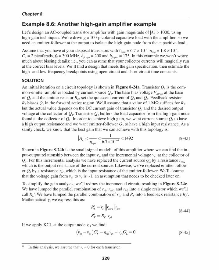
Chapter 8
228
Example 8.6: Another high-gain amplifi er exampleLet’s design an AC-coupled transistor amplifi er with gain magnitude of |Av| > 1000, using high-gain techniques. We’re driving a 100-picofarad capacitive load with the amplifi er, so we need an emitter-follower at the output to isolate the high-gain node from the capacitive load.
Assume that you have at your disposal transistors with ηnpn = 6.7 × 10⁻⁴, ηpnp = 1.8 × 10⁻⁴, Cμ = 2 picofarads, fT = 300 MHz, hfe,npn = 200 and hfe,pnp = 175. In this example we won’t worry much about biasing details; i.e., you can assume that your collector currents will magically run at the correct bias levels. We’ll fi nd a design that meets the gain specifi cation, then estimate the high- and low-frequency breakpoints using open-circuit and short-circuit time constants.
SOLUTIONAn initial iteration on a circuit topology is shown in Figure 8-24a. Transistor Q1 is the com-mon-emitter amplifi er loaded by current source Q2. The base bias voltage VBIAS2 at the base of Q2 and the emitter resistor RE2 set the quiescent current of Q1 and Q2. Feedback resistor RF biases Q1 in the forward active region. We’ll assume that a value of 1 MΩ suffi ces for RF, but the actual value depends on the DC current gain of transistor Q1 and the desired output voltage at the collector of Q1. Transistor Q3 buffers the load capacitor from the high-gain node found at the collector of Q1. In order to achieve high gain, we want current source Q2 to have a high output resistance and we want emitter-follower Q3 to have a high input resistance. As a sanity check, we know that the best gain that we can achieve with this topology is:
4
1 11492
6.7 10vnpn
Aη −< < <
× [8-43]
Shown in Figure 8-24b is the small-signal model11 of this amplifi er where we can fi nd the in-put-output relationship between the input vin and the incremental voltage vc1 at the collector of Q1. For this incremental analysis we have replaced the current source Q2 by a resistance rout2 which is the output resistance of the current source. Likewise, we’ve replaced emitter-follow-er Q3 by a resistance rin3 which is the input resistance of the emitter-follower. We’ll assume that the voltage gain from vc1 to vo is ∼1, an assumption that needs to be checked later on.
To simplify the gain analysis, we’ll redraw the incremental circuit, resulting in Figure 8-24c. We have lumped the parallel combination of ro1, rout2 and rin3 into a single resistor which we’ll call RL'. We have lumped the parallel combination of rμ1 and RF into a feedback resistance RF'. Mathematically, we express this as:
1 2 3
1
L o out in
F F
R r r r
R R rμ
′ =
′ = [8-44]
If we apply KCL at the output node vc1 we fi nd:
( )1 1 1 0in c F m in c Lv v G g v v G′ ′− − − = [8-45]
11 In this analysis, we assume that rx = 0 for each transistor.
Thompson Book.indb 228 3/20/2006 11:35:33 AM
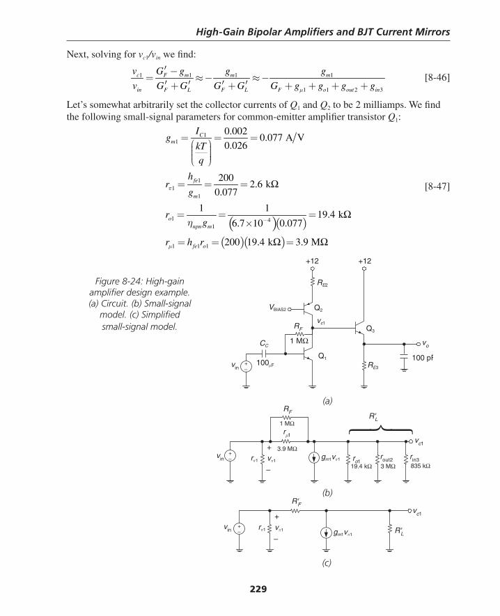
High-Gain Bipolar Amplifi ers and BJT Current Mirrors
229
Next, solving for vc1/vin we fi nd:
1 1 1 1
1 1 2 3
c F m m m
in F L F L F o out in
v G g g g
v G G G G G g g g gμ
′ −= ≈ − ≈ −
′ ′ ′ ′+ + + + + + [8-46]
Let’s somewhat arbitrarily set the collector currents of Q1 and Q2 to be 2 milliamps. We fi nd the following small-signal parameters for common-emitter amplifi er transistor Q1:
( )( )
( )( )
11
11
1
1 41
1 1 1
0.0020.077 A V
0.026
2002.6 k
0.077
1 119.4 k
6.7 10 0.077
200 19.4 k 3.9 M
Cm
fe
m
onpn m
fe o
Ig
kT
q
hr
g
rg
r h r
π
μ
η −
= = =⎛ ⎞⎟⎜ ⎟⎜ ⎟⎜ ⎟⎝ ⎠
= = =
= = =×
= = =
Ω
Ω
Ω Ω
[8-47]
Q1
Q2
RF
vo
+–
vin
CC
VBIAS2
RE2
100 pF100μF
1 MΩ
+12 +12
RE3
Q3
vc1
vc1
+–
+
–
ro1vin rout2 rin3gm1vπ1vπ1rπ1
3.9 MΩ
1 MΩ
RF
rμ1
19.4 kΩ 835 kΩ3 MΩ
R'L ⎧⎨⎩
+–
+
–gm1vπ1
vπ1rπ1 R'L
vc1
R'F
vin
(a)
(b)
Figure 8-24: High-gain amplifi er design example.(a) Circuit. (b) Small-signal
model. (c) Simplifi ed small-signal model.
(c)
Thompson Book.indb 229 3/20/2006 11:35:34 AM
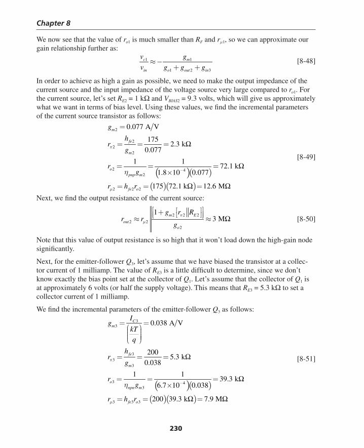
Chapter 8
230
We now see that the value of ro1 is much smaller than RF and rμ1, so we can approximate our gain relationship further as:
1 1
1 2 3
c m
in o out in
v g
v g g g≈ −
+ + [8-48]
In order to achieve as high a gain as possible, we need to make the output impedance of the current source and the input impedance of the voltage source very large compared to ro1. For the current source, let’s set RE2 = 1 kΩ and VBIAS2 = 9.3 volts, which will give us approximately what we want in terms of bias level. Using these values, we fi nd the incremental parameters of the current source transistor as follows:
( )( )
( )( )
2
22
2
2 42
2 2 2
0.077 A V
1752.3 k
0.077
1 172.1 k
1.8 10 0.077
175 72.1 k 12.6 M
m
fe
m
opnp m
fe o
g
hr
g
rg
r h r
π
μ
η −
=
= = =
= = =×
= = =
Ω
Ω
Ω Ω
[8-49]
Next, we fi nd the output resistance of the current source:
2 2 2
2 22
13 M
m E
outo
g r Rr r
g
π
μ
⎡ ⎤⎡ ⎤+⎢ ⎥⎣ ⎦⎣ ⎦≈ ≈ Ω [8-50]
Note that this value of output resistance is so high that it won’t load down the high-gain node signifi cantly.
Next, for the emitter-follower Q3, let’s assume that we have biased the transistor at a collec-tor current of 1 milliamp. The value of RE3 is a little diffi cult to determine, since we don’t know exactly the bias point set at the collector of Q1. Let’s assume that the collector of Q1 is at approximately 6 volts (or half the supply voltage). This means that RE3 = 5.3 kΩ to set a collector current of 1 milliamp.
We fi nd the incremental parameters of the emitter-follower Q3 as follows:
( )( )
( )( )
33
33
3
3 43
3 3 3
0.038 A V
2005.3 k
0.038
1 139.3 k
6.7 10 0.038
200 39.3 k 7.9 M
Cm
fe
m
onpn m
fe o
Ig
kT
q
hr
g
rg
r h r
π
μ
η −
= =⎛ ⎞⎟⎜ ⎟⎜ ⎟⎜ ⎟⎝ ⎠
= = =
= = =×
= = =
Ω
Ω
Ω Ω
[8-51]
Thompson Book.indb 230 3/20/2006 11:35:34 AM
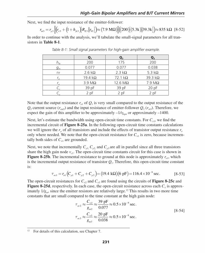
High-Gain Bipolar Amplifi ers and BJT Current Mirrors
231
Next, we fi nd the input resistance of the emitter-follower:
( )( ) ( ) ( )( )( )3 3 3 3 3 031 7.9 M 200 5.3k 39.3k 835 kin fe Er r r h R rμ π⎡ ⎤⎡ ⎤= + + ≈ ≈⎣ ⎦ ⎣ ⎦Ω Ω [8-52]
In order to continue with the analysis, we’ll tabulate the small-signal parameters for all tran-sistors in Table 8-1.
Table 8-1: Small signal parameters for high-gain amplifi er example.
Q1 Q2 Q3
hfe 200 175 200gm 0.077 0.077 0.038rπ 2.6 kΩ 2.3 kΩ 5.3 kΩro 19.4 kΩ 72.1 kΩ 39.3 kΩrμ 3.9 MΩ 12.6 MΩ 7.9 MΩCπ 39 pF 39 pF 20 pFCμ 2 pF 2 pF 2 pF
Note that the output resistance ro1 of Q1 is very small compared to the output resistance of the Q2 current source (rout2) and the input resistance of emitter-follower Q3 (rin3). Therefore, we expect the gain of this amplifi er to be approximately –1/ηnpn or approximately –1400.
Next, let’s estimate the bandwidth using open-circuit time constants. For Cπ1, we fi nd the incremental circuit of Figure 8-25a. In the following open-circuit time constants calculations we will ignore the rμ of all transistors and include the effects of transistor output resistance ro only where needed. We note that the open-circuit resistance for Cπ1 is zero, because incremen-tally both sides of Cπ1 are grounded.
Next, we note that incrementally Cμ1, Cμ2, and Cμ3 are all in parallel since all three transistors share the high gain node vc1. The open-circuit time constants circuit for this case is shown in Figure 8-25b. The incremental resistance to ground at this node is approximately ro1, which is the incremental output resistance of transistor Q1. Therefore, this open-circuit time constant is:
( ) ( )( ) 91 1 1 2 3 19.4 k 6 pF 116.4 10 sec.oc or C C Cμ μ μτ −= + + = = ×Ω [8-53]
The open-circuit resistances for Cπ2 and Cπ3 are found using the circuits of Figure 8-25c and Figure 8-25d, respectively. In each case, the open-circuit resistance across each Cπ is approx-imately 1/gm, since the emitter resistors are relatively large.12 This results in two more time constants that are small compared to the time constant at the high gain node:
922
2
933
3
39 pF0.5 10 sec.
0.077
20 pF0.5 10 sec.
0.038
ocm
ocm
C
g
C
g
π
π
τ
τ
−
−
≈ ≈ ≈ ×
≈ ≈ ≈ × [8-54]
12 For details of this calculation, see Chapter 7.
Thompson Book.indb 231 3/20/2006 11:35:35 AM
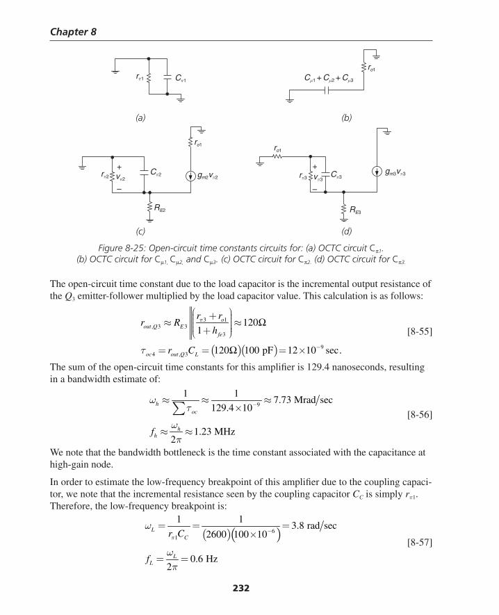
Chapter 8
232
(a) (b)
(c) (d)
Figure 8-25: Open-circuit time constants circuits for: (a) OCTC circuit Cπ1. (b) OCTC circuit for Cμ1, Cμ2, and Cμ3. (c) OCTC circuit for Cπ2. (d) OCTC circuit for Cπ3.
The open-circuit time constant due to the load capacitor is the incremental output resistance of the Q3 emitter-follower multiplied by the load capacitor value. This calculation is as follows:
( )( )
3 1, 3 3
3
94 , 3
1201
120 100 pF 12 10 sec.
oout Q E
fe
oc out Q L
r rr R
h
r C
π
τ −
⎛ ⎞+ ⎟⎜ ⎟⎜≈ ≈⎟⎜ ⎟⎜ ⎟+⎝ ⎠
= = = ×
Ω
Ω
[8-55]
The sum of the open-circuit time constants for this amplifi er is 129.4 nanoseconds, resulting in a bandwidth estimate of:
9
1 17.73 Mrad sec
129.4 10
1.23 MHz2
hoc
hhf
ωτ
ωπ
−≈ ≈ ≈×
≈ ≈
∑ [8-56]
We note that the bandwidth bottleneck is the time constant associated with the capacitance at high-gain node.
In order to estimate the low-frequency breakpoint of this amplifi er due to the coupling capaci-tor, we note that the incremental resistance seen by the coupling capacitor CC is simply rπ1. Therefore, the low-frequency breakpoint is:
( )( )6
1
1 13.8 rad sec
2600 100 10
0.6 Hz2
LC
LL
r C
f
π
ω
ωπ
−= = =
×
= =
[8-57]
RE2
Cπ1rπ1 Cμ1 + Cμ2 + Cμ3
ro1
rπ2 vπ2Cπ2
ro1
gm2vπ2
+
–
Cπ3
RE3
rπ3 vπ3
gm3vπ3+
–
ro1
Thompson Book.indb 232 3/20/2006 11:35:35 AM
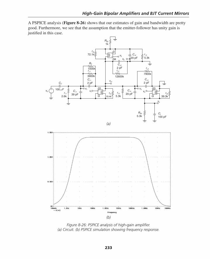
High-Gain Bipolar Amplifi ers and BJT Current Mirrors
233
A PSPICE analysis (Figure 8-26) shows that our estimates of gain and bandwidth are pretty good. Furthermore, we see that the assumption that the emitter-follower has unity gain is justifi ed in this case.
vin
rμ3
rπ1
2.6k
+–
100 μF
CC
Cπ1
39 pF
RF
3900kCμ1
2 pF
1000krμ1
G
G1v1v1
+
–
+
–
+
–G
G
G3
G4
v3v3
vo
v2
v2
Cπ2
20 pF
Cπ3
20 pF
CL
100 pF
RE3
5.3k
ro3
39.3k
Cμ3
2 pF
ro1
19.4k
ro2
72.1k
RE2
1k
vc1
rπ2
5.3k
12600k
rπ3
5.3k
Cμ2
2 pFrμ2
7900k
(a)
(b)
Figure 8-26: PSPICE analysis of high-gain amplifi er. (a) Circuit. (b) PSPICE simulation showing frequency response.
Thompson Book.indb 233 3/20/2006 11:35:36 AM
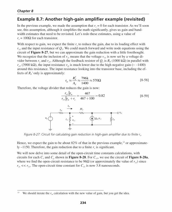
Chapter 8
234
Example 8.7: Another high-gain amplifi er example (revisited)In the previous example, we made the assumption that rx = 0 for each transistor. As we’ll soon see, this assumption, although it simplifi es the math signifi cantly, gives us gain and band-width estimates that need to be revisited. Let’s redo these estimates, using a value of rx = 100Ω for each transistor.
With respect to gain, we expect the fi nite rx to reduce the gain, due to its loading effect with rπ1 and the input resistance of Q1. We could march forward and write node equations using the circuit of Figure 8-27, but we can approximate the gain reduction with a little forethought. We recognize that the inclusion of rx1 means that the voltage vπ1 is now set by a voltage di-vider between rπ and rx1. Although the feedback resistor of Q1 is RF (1000 kΩ) in parallel with rμ1 (3900 kΩ), the input resistance rin is much lower due to the high negative gain (~ –1400) around this resistance. The input resistance looking into the transistor base, including the ef-fects of RF' only is approximately:
796k570
1400F
inV
Rr
A
′≈ ≈ ≈ Ω [8-58]
Therefore, the voltage divider that reduces the gain is now:
1
1
4670.82
467 100in
in x
r r
r r rπ
π
= =+ +
[8-59]
Figure 8-27: Circuit for calculating gain reduction in high-gain amplifi er due to fi nite rx.
Hence, we expect the gain to be about 82% of that in the previous example,13 or approximate-ly –1150. Therefore, the gain reduction due to a fi nite rx is signifi cant.
We will now delve into some detail of the open-circuit time constants calculations, with circuits for each Cπ and Cμ shown in Figure 8-28. For Cπ1, we use the circuit of Figure 8-28a, where we fi nd the open-circuit resistance to be 96Ω (or approximately the value of rx1) since rx1 << rπ1. The open-circuit time constant for Cπ1 is now 3.8 nanoseconds.
vin rπ1
R'F
vπ1
rx1vc1
rin
ro1gm1vπ1
+
–
+–
13 We should iterate the rin calculation with the new value of gain, but you get the idea.
Thompson Book.indb 234 3/20/2006 11:35:36 AM
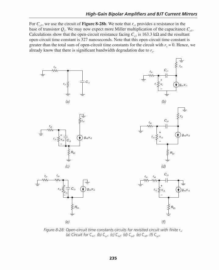
High-Gain Bipolar Amplifi ers and BJT Current Mirrors
235
For Cμ1, we use the circuit of Figure 8-28b. We note that rx1 provides a resistance in the base of transistor Q1. We may now expect more Miller multiplication of the capacitance Cμ1. Calculations show that the open-circuit resistance facing Cμ1 is 163.3 kΩ and the resultant open-circuit time constant is 327 nanoseconds. Note that this open-circuit time constant is greater than the total sum of open-circuit time constants for the circuit with rx = 0. Hence, we already know that there is signifi cant bandwidth degradation due to rx.
rx1
rπ1Cπ1
rx2
rπ2 Cπ2vπ2
+
–
RE2
ro1
gm2vπ2
Cμ2
vπ2
+
–
RE2
ro1
gm2vπ2
rx2
rπ2
Cπ3
vπ3
+
–
RE3
ro1
gm3vπ3
rx3
rπ3
Cμ3
vπ3
+
–
RE3
ro1
gm3vπ3
rx3
rπ3
Cμ1
vπ
+
–
ro1
gm1vπ1rπ
rx1
(a) (b)
(c) (d)
(e) (f)
Figure 8-28: Open-circuit time constants circuits for revisited circuit with fi nite rx. (a) Circuit for Cπ1. (b) Cμ1. (c) Cπ2. (d) Cμ2. (e) Cπ3. (f) Cμ3.
Thompson Book.indb 235 3/20/2006 11:35:37 AM
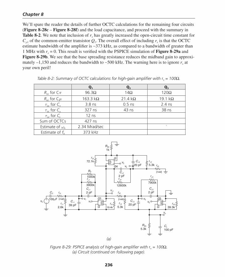
Chapter 8
236
We’ll spare the reader the details of further OCTC calculations for the remaining four circuits (Figure 8-28c – Figure 8-28f) and the load capacitance, and proceed with the summary in Table 8-2. We note that inclusion of rx has greatly increased the open-circuit time constant for Cμ1 of the common-emitter transistor Q1. The overall effect of including rx is that the OCTC estimate bandwidth of the amplifi er is ∼373 kHz, as compared to a bandwidth of greater than 1 MHz with rx = 0. This result is verifi ed with the PSPICE simulation of Figure 8-29a and Figure 8-29b. We see that the base spreading resistance reduces the midband gain to approxi-mately –1,150 and reduces the bandwidth to ∼500 kHz. The warning here is to ignore rx at your own peril!
Table 8-2: Summary of OCTC calculations for high-gain amplifi er with rx = 100Ω.
Q1 Q2 Q3
Roc for Cπ 96.3Ω 14Ω 120ΩRoc for Cμ 163.3 kΩ 21.4 kΩ 19.1 kΩτoc for Cπ 3.8 ns 0.5 ns 2.4 nsτoc for Cμ 327 ns 43 ns 38 nsτoc for CL 12 ns
Sum of OCTCs 427 nsEstimate of ωh 2.34 Mrad/sec `Estimate of fh 373 kHz
vin
rμ3
rπ1
2.6k
+–
100μF
CC
Cπ1
39 pF
RF
3900kCμ1
2 pF
1000krμ1
G
G1v1v1
+
–
+
–
+
–G
G
G3
G4
v3v3
vo
v2
v2
Cπ2
20 pF
Cπ3
20 pF
CL
100 pF
RE3
5.3k
ro3
39.3k
Cμ3
2 pF
ro1
19.4k
ro2
72.1k
RE2
1k
vc1
rπ2
5.3k
12600k
rπ3
5.3k
Cμ2
2 pFrμ2
7900k
rx1
{rval} {rval}
{rval}
rx2
rx3
(a)
Figure 8-29: PSPICE analysis of high-gain amplifi er with rx = 100Ω. (a) Circuit (continued on following page).
Thompson Book.indb 236 3/20/2006 11:35:37 AM
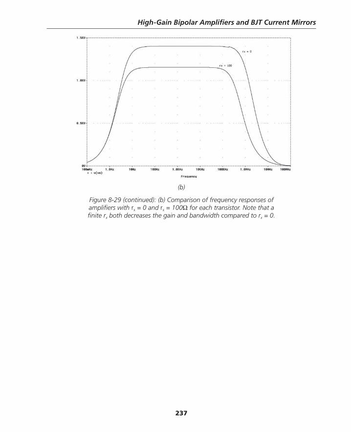
High-Gain Bipolar Amplifi ers and BJT Current Mirrors
237
(b)
Figure 8-29 (continued): (b) Comparison of frequency responses of amplifi ers with rx = 0 and rx = 100Ω for each transistor. Note that afi nite rx both decreases the gain and bandwidth compared to rx = 0.
Thompson Book.indb 237 3/20/2006 11:35:38 AM
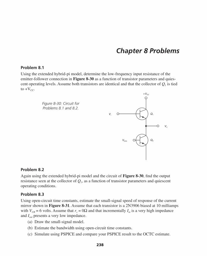
238
Chapter 8 Problems
Problem 8.1Using the extended hybrid-pi model, determine the low-frequency input resistance of the emitter-follower connection in Figure 8-30 as a function of transistor parameters and quies-cent operating levels. Assume both transistors are identical and that the collector of Q1 is tied to +VCC.
Q1
Q2Vbias
Vi
Vo
+VCC
Figure 8-30: Circuit for Problems 8.1 and 8.2.
Problem 8.2Again using the extended hybrid-pi model and the circuit of Figure 8-30, fi nd the output resistance seen at the collector of Q1, as a function of transistor parameters and quiescent operating conditions.
Problem 8.3Using open-circuit time constants, estimate the small-signal speed of response of the current mirror shown in Figure 8-31. Assume that each transistor is a 2N3906 biased at 10 milliamps with VCB = 6 volts. Assume that rx = 0Ω and that incrementally Iin is a very high impedance and Iout presents a very low impedance.
(a) Draw the small-signal model.
(b) Estimate the bandwidth using open-circuit time constants.
(c) Simulate using PSPICE and compare your PSPICE result to the OCTC estimate.
Thompson Book.indb 238 3/20/2006 11:35:38 AM
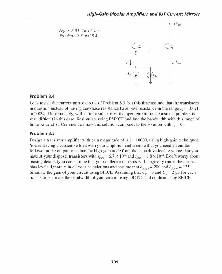
High-Gain Bipolar Amplifi ers and BJT Current Mirrors
239
Problem 8.4Let’s revisit the current mirror circuit of Problem 8.3, but this time assume that the transistors in question instead of having zero base resistance have base resistance in the range rx = 100Ω to 200Ω . Unfortunately, with a fi nite value of rx, the open-circuit time constants problem is very diffi cult in this case. Resimulate using PSPICE and fi nd the bandwidth with this range of fi nite value of rx. Comment on how this solution compares to the solution with rx = 0.
Problem 8.5Design a transistor amplifi er with gain magnitude of |Av| = 10000, using high-gain techniques. You're driving a capacitive load with your amplifi er, and assume that you need an emitter- follower at the output to isolate the high gain node from the capacitive load. Assume that you have at your disposal transistors with ηnpn = 6.7 × 10⁻⁴ and ηpnp = 1.8 × 10⁻⁴. Don’t worry about biasing details (you can assume that your collector currents will magically run at the correct bias levels. Ignore rx in all your calculations and assume that hfe,npn = 200 and hfe,pnp = 175. Simulate the gain of your circuit using SPICE. Assuming that Cπ = 0 and Cμ = 2 pF for each transistor, estimate the bandwidth of your circuit using OCTCs and confi rm using SPICE.
IOUTIIN
Q2Q1
+VCC
IIN iin
Figure 8-31: Circuit for Problems 8.3 and 8.4.
Thompson Book.indb 239 3/20/2006 11:35:39 AM
Chapter 8
240
ReferencesEarly, J. M., “Effects of Space-Charge Layer Widening in Junction Transistors,” Proceedings
of the I.R.E., 1952, pp. 1401–1406.Gray, P. E., DeWitt, D., Boothroyd, A. R., and Gibbons, J. F., Physical Electronics and Cir-
cuit Models of Transistors, Semiconductor Electronics Education Committee, volume 2, John Wiley, 1964.
Gray, Paul R., Hurst, Paul J., Lewis, Stephen H., and Meyer, Robert G., Analysis and Design of Analog Integrated Circuits, 4th edition, John Wiley, 2001.
Grebene, Alan B., Bipolar and MOS Analog Integrated Circuit Design, John Wiley, 1984.Hart, B. L., “Modeling the Early Effect in Bipolar Transistors,” IEEE Journal of Solid State
Circuits, vol. 18, no. 1, February 1983, pp. 139–140.Huiting, Chen, Whiteside, F., and Geiger, R., “Current Mirror Circuit with Accurate Mirror
Gain for Low β Transistors,” Proceedings of the 2001 IEEE International Symposium on Circuits and Systems, (ISCAS 2001), May 6–9, 2001, pp. 536–539.
Joardar, K., “A New Approach for Extracting Base Width Modulation Parameters in Bipolar Transistors,” Proceedings of the 1994 Bipolar/BiCMOS Circuits and Technology Meet-ing, October 1994, pp. 140–143.
Kimura, K., “Low Voltage Techniques for Bias Circuits,” IEEE Transactions on Circuits and Systems I: Fundamental Theory and Applications, vol. 5, May 1997, pp. 459–465.
Liou, J. J., “Comments on ‘Early Voltage in Very-Narrow-base Bipolar Transistors,’ by D. J. Roulston” IEEE Electron Device Letters, vol. 11, no. 5, May 1990, p. 236.
Mahattanakul, J., Pookaiyaudom, S., and Toumazou, C., “Understanding Wilson Current Mir-ror via the Negative Feedback Approach,” Proceedings of the 2001 IEEE International Symposium on Circuits and Systems, (ISCAS 2001), May 6–9, 2001, pp. 532–535.
McAndrew, C. C., and Nagel, L. W., “SPICE Early Modeling [Bipolar Transistors],” Proceedings of the 1994 Bipolar/BiCMOS Circuits and Technology Meeting, October 10–11, 1994, pp 144–147.
Roberge, James K., Operational Amplifi ers: Theory and Practice, John Wiley, 1975.Roulston, D. J., “Early Voltage in Very-Narrow-base Bipolar Transistors,” IEEE Journal of
Solid State Circuits, vol. 11, no. 2, February 1990, pp. 88–89.Rucker, L. M., “Monolithic Bipolar Diodes and Their Models,” IEEE Circuits and Devices
Magazine, vol. 7, no. 2, March 1991, pp. 26–31. Soclof, Sidney, Analog Integrated Circuits, Prentice-Hall, 1985.Thompson, Marc T., “Tips for Designing High-Gain Amplifi ers,” Electronic Design, May 16,
1994, pp. 83–90.van Kessel, J., and van de Plassche, R. J., “Integrated Linear Basic Circuits,” Philips Techni-
cal Review, vol. 32, no. 1, 1971, pp. 1–10.Yuan, J. S., and Liou, J. J., “An Improved Early Voltage Model for Advanced Bipolar Tran-
sistors,” IEEE Transactions on Electron Devices, vol. 38, no. 1, January 1991, pp. 179–182.
Thompson Book.indb 240 3/20/2006 11:35:39 AM
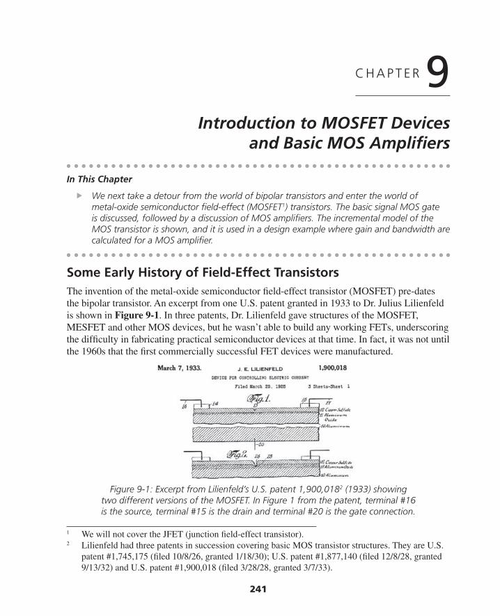
241
C H A P T E R 9Introduction to MOSFET Devices
and Basic MOS Amplifi ers
Some Early History of Field-Effect TransistorsThe invention of the metal-oxide semiconductor fi eld-effect transistor (MOSFET) pre-dates the bipolar transistor. An excerpt from one U.S. patent granted in 1933 to Dr. Julius Lilienfeld is shown in Figure 9-1. In three patents, Dr. Lilienfeld gave structures of the MOSFET, MESFET and other MOS devices, but he wasn’t able to build any working FETs, underscoring the diffi culty in fabricating practical semiconductor devices at that time. In fact, it was not until the 1960s that the fi rst commercially successful FET devices were manufactured.
In This Chapter
We next take a detour from the world of bipolar transistors and enter the world of metal-oxide semiconductor fi eld-effect (MOSFET1) transistors. The basic signal MOS gate is discussed, followed by a discussion of MOS amplifi ers. The incremental model of the MOS transistor is shown, and it is used in a design example where gain and bandwidth are calculated for a MOS amplifi er.
1 We will not cover the JFET (junction fi eld-effect transistor).2 Lilienfeld had three patents in succession covering basic MOS transistor structures. They are U.S.
patent #1,745,175 (fi led 10/8/26, granted 1/18/30); U.S. patent #1,877,140 (fi led 12/8/28, granted 9/13/32) and U.S. patent #1,900,018 (fi led 3/28/28, granted 3/7/33).
Figure 9-1: Excerpt from Lilienfeld’s U.S. patent 1,900,0182 (1933) showing two different versions of the MOSFET. In Figure 1 from the patent, terminal #16 is the source, terminal #15 is the drain and terminal #20 is the gate connection.
Thompson Book.indb 241 3/20/2006 11:35:39 AM
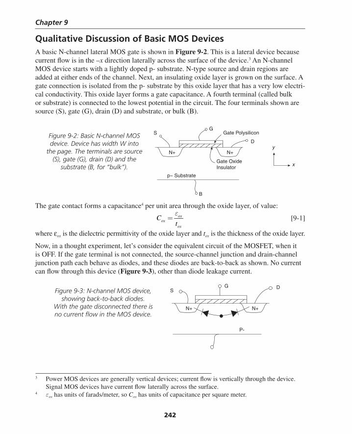
Chapter 9
242
Qualitative Discussion of Basic MOS DevicesA basic N-channel lateral MOS gate is shown in Figure 9-2. This is a lateral device because current fl ow is in the –x direction laterally across the surface of the device.3 An N-channel MOS device starts with a lightly doped p- substrate. N-type source and drain regions are added at either ends of the channel. Next, an insulating oxide layer is grown on the surface. A gate connection is isolated from the p- substrate by this oxide layer that has a very low electri-cal conductivity. This oxide layer forms a gate capacitance. A fourth terminal (called bulk or substrate) is connected to the lowest potential in the circuit. The four terminals shown are source (S), gate (G), drain (D) and substrate, or bulk (B).
3 Power MOS devices are generally vertical devices; current fl ow is vertically through the device. Signal MOS devices have current fl ow laterally across the surface.
4 εox has units of farads/meter, so Cox has units of capacitance per square meter.
The gate contact forms a capacitance4 per unit area through the oxide layer, of value:
oxox
ox
Ct
ε= [9-1]
where εox is the dielectric permittivity of the oxide layer and tox is the thickness of the oxide layer.
Now, in a thought experiment, let’s consider the equivalent circuit of the MOSFET, when it is OFF. If the gate terminal is not connected, the source-channel junction and drain-channel junction path each behave as diodes, and these diodes are back-to-back as shown. No current can fl ow through this device (Figure 9-3), other than diode leakage current.
N+ N+
SG
Dy
x
B
Gate Polysilicon
Gate OxideInsulator
p− Substrate
N+ N+
SG D
P-
Figure 9-2: Basic N-channel MOS device. Device has width W into
the page. The terminals are source (S), gate (G), drain (D) and the
substrate (B, for “bulk”).
Figure 9-3: N-channel MOS device, showing back-to-back diodes.
With the gate disconnected there is no current fl ow in the MOS device.
Thompson Book.indb 242 3/20/2006 11:35:40 AM
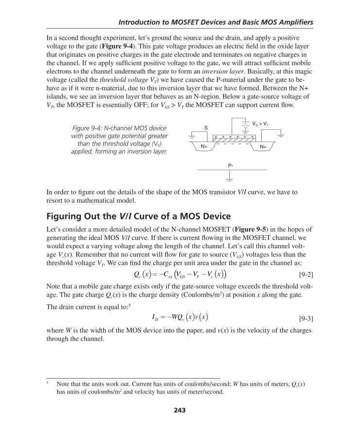
Introduction to MOSFET Devices and Basic MOS Amplifi ers
243
In a second thought experiment, let’s ground the source and the drain, and apply a positive voltage to the gate (Figure 9-4). This gate voltage produces an electric fi eld in the oxide layer that originates on positive charges in the gate electrode and terminates on negative charges in the channel. If we apply suffi cient positive voltage to the gate, we will attract suffi cient mobile electrons to the channel underneath the gate to form an inversion layer. Basically, at this magic voltage (called the threshold voltage VT) we have caused the P-material under the gate to be-have as if it were n-material, due to this inversion layer that we have formed. Between the N+ islands, we see an inversion layer that behaves as an N-region. Below a gate-source voltage of VT, the MOSFET is essentially OFF; for VGS > VT the MOSFET can support current fl ow.
In order to fi gure out the details of the shape of the MOS transistor V/I curve, we have to resort to a mathematical model.
Figuring Out the V/I Curve of a MOS DeviceLet’s consider a more detailed model of the N-channel MOSFET (Figure 9-5) in the hopes of generating the ideal MOS V/I curve. If there is current fl owing in the MOSFET channel, we would expect a varying voltage along the length of the channel. Let’s call this channel volt-age Vc(x). Remember that no current will fl ow for gate to source (VGS) voltages less than the threshold voltage VT. We can fi nd the charge per unit area under the gate in the channel as:
( ) ( )( )c ox GS T cQ x C V V V x= − − − [9-2]
Note that a mobile gate charge exists only if the gate-source voltage exceeds the threshold volt-age. The gate charge Qc(x) is the charge density (Coulombs/m2) at position x along the gate.
The drain current is equal to: 5
( ) ( )D cI WQ x v x= − [9-3]
where W is the width of the MOS device into the paper, and v(x) is the velocity of the charges through the channel.
N+ N+
S
P-
VG > VT
+ + + + + +
− − − − −
Figure 9-4: N-channel MOS device with positive gate potential greater
than the threshold voltage (VT) applied, forming an inversion layer.
5 Note that the units work out. Current has units of coulombs/second; W has units of meters, Qc(x) has units of coulombs/m2 and velocity has units of meter/second.
Thompson Book.indb 243 3/20/2006 11:35:41 AM
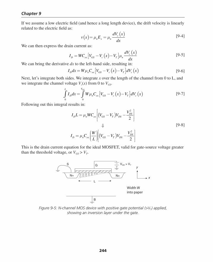
Chapter 9
244
If we assume a low electric fi eld (and hence a long length device), the drift velocity is linearly related to the electric fi eld as:
( )( )c
n x n
dV xv x E
dxμ μ= = [9-4]
We can then express the drain current as:
( )( )c
D ox GS c T n
dV xI WC V V x V
dxμ⎡ ⎤= − −⎣ ⎦
[9-5]
We can bring the derivative dx to the left-hand side, resulting in:
( ) ( )D n ox GS c T cI dx W C V V x V dV xμ ⎡ ⎤= − −⎣ ⎦ [9-6]
Next, let’s integrate both sides. We integrate x over the length of the channel from 0 to L, and we integrate the channel voltage Vc(x) from 0 to VGS.
( ) ( )0 0
GSVL
D n ox GS c T cI dx W C V V x V dV xμ ⎡ ⎤= − −⎣ ⎦∫ ∫ [9-7]
Following out this integral results in:
( )
( )
2
2
2
2
DSD n ox GS T DS
DSD n ox GS T DS
VI L WC V V V
VWI C V V V
L
μ
μ
⎡ ⎤⎢ ⎥= − −⎢ ⎥⎣ ⎦
⇓⎡ ⎤⎛ ⎞⎟⎜ ⎢ ⎥= − −⎟⎜ ⎟⎢ ⎥⎜⎝ ⎠⎣ ⎦
[9-8]
This is the drain current equation for the ideal MOSFET, valid for gate-source voltage greater than the threshold voltage, or VGS > VT.
Figure 9-5: N-channel MOS device with positive gate potential (>VT) applied, showing an inversion layer under the gate.
N+ N+
S
B
VGS > VTGy
x
Width Winto paper
L
–
–
–
–
–
–
–
–
––
––
Thompson Book.indb 244 3/20/2006 11:35:41 AM
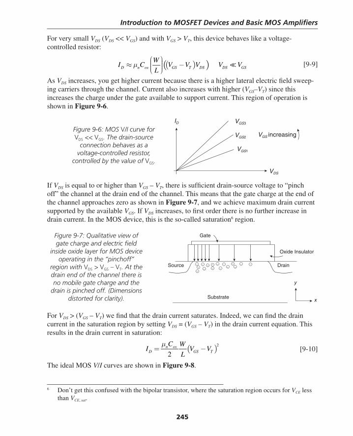
Introduction to MOSFET Devices and Basic MOS Amplifi ers
245
For very small VDS (VDS << VGS) and with VGS > VT, this device behaves like a voltage- controlled resistor:
( )( )D n ox GS T DS DS GS
WI C V V V V V
Lμ
⎛ ⎞⎟⎜≈ −⎟⎜ ⎟⎜⎝ ⎠ [9-9]
As VDS increases, you get higher current because there is a higher lateral electric fi eld sweep-ing carriers through the channel. Current also increases with higher (VGS–VT) since this increases the charge under the gate available to support current. This region of operation is shown in Figure 9-6.
ID VGS3
VGS2
VGS1
VGS increasing
VDS
6 Don’t get this confused with the bipolar transistor, where the saturation region occurs for VCE less than VCE, sat.
If VDS is equal to or higher than VGS – VT, there is suffi cient drain-source voltage to “pinch off” the channel at the drain end of the channel. This means that the gate charge at the end of the channel approaches zero as shown in Figure 9-7, and we achieve maximum drain current supported by the available VGS. If VDS increases, to fi rst order there is no further increase in drain current. In the MOS device, this is the so-called saturation6 region.
y
x
–
Substrate
Oxide Insulator
Gate
Source Drain–
–
–
–
– –
–
–
–
––
–
–– –
Figure 9-6: MOS V/I curve for VDS << VGS. The drain-source
connection behaves as a voltage-controlled resistor,
controlled by the value of VGS.
Figure 9-7: Qualitative view of gate charge and electric fi eld
inside oxide layer for MOS device operating in the “pinchoff”
region with VDS > VGS – VT. At the drain end of the channel there is no mobile gate charge and the
drain is pinched off. (Dimensions distorted for clarity).
For VDS > (VGS – VT) we fi nd that the drain current saturates. Indeed, we can fi nd the drain current in the saturation region by setting VDS = (VGS – VT) in the drain current equation. This results in the drain current in saturation:
( )2
2n ox
D GS T
C WI V V
L
μ= − [9-10]
The ideal MOS V/I curves are shown in Figure 9-8.
Thompson Book.indb 245 3/20/2006 11:35:42 AM
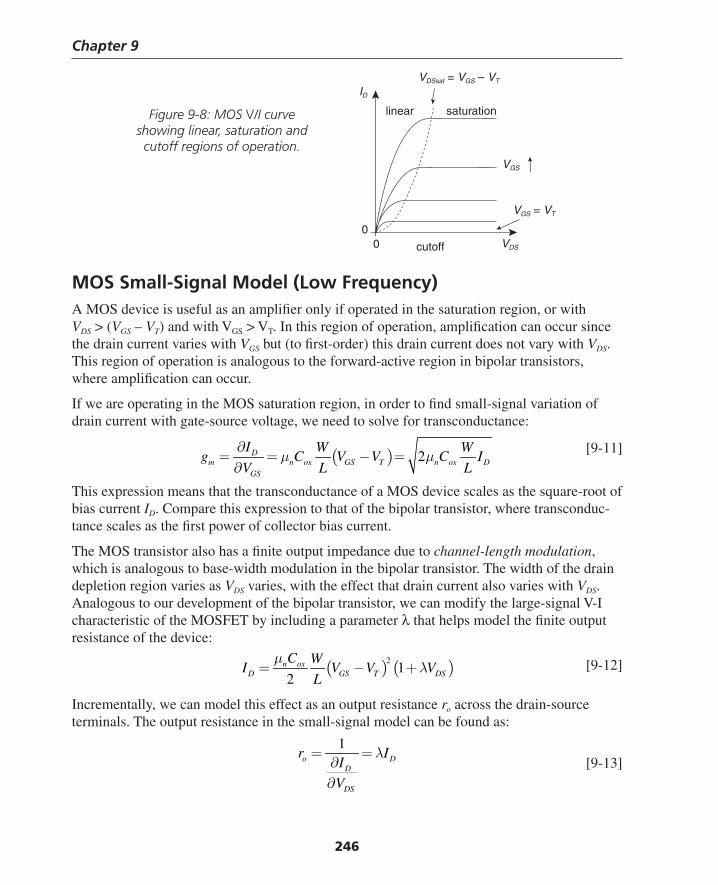
Chapter 9
246
MOS Small-Signal Model (Low Frequency)A MOS device is useful as an amplifi er only if operated in the saturation region, or withVDS > (VGS – VT) and with VGS > VT. In this region of operation, amplifi cation can occur since the drain current varies with VGS but (to fi rst-order) this drain current does not vary with VDS. This region of operation is analogous to the forward-active region in bipolar transistors, where amplifi cation can occur.
If we are operating in the MOS saturation region, in order to fi nd small-signal variation of drain current with gate-source voltage, we need to solve for transconductance:
( ) 2Dm n ox GS T n ox D
GS
I W Wg C V V C I
V L Lμ μ
∂= = − =
∂ [9-11]
This expression means that the transconductance of a MOS device scales as the square-root of bias current ID. Compare this expression to that of the bipolar transistor, where transconduc-tance scales as the fi rst power of collector bias current.
The MOS transistor also has a fi nite output impedance due to channel-length modulation, which is analogous to base-width modulation in the bipolar transistor. The width of the drain depletion region varies as VDS varies, with the effect that drain current also varies with VDS. Analogous to our development of the bipolar transistor, we can modify the large-signal V-I characteristic of the MOSFET by including a parameter λ that helps model the fi nite output resistance of the device:
( ) ( )21
2n ox
D GS T DS
C WI V V V
L
μλ= − + [9-12]
Incrementally, we can model this effect as an output resistance ro across the drain-source terminals. The output resistance in the small-signal model can be found as:
1
o DD
DS
r II
V
λ= =∂∂
[9-13]
saturationlinear
cutoff VDS
VGS = VT
VGS
VDSsat = VGS – VT
ID
00
Figure 9-8: MOS V/I curve showing linear, saturation and cutoff regions of operation.
Thompson Book.indb 246 3/20/2006 11:35:43 AM
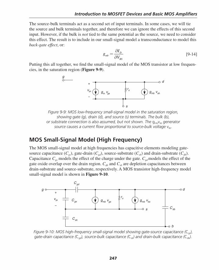
Introduction to MOSFET Devices and Basic MOS Amplifi ers
247
The source-bulk terminals act as a second set of input terminals. In some cases, we will tie the source and bulk terminals together, and therefore we can ignore the effects of this second input. However, if the bulk is not tied to the same potential as the source, we need to consider this effect. The result is to include in our small-signal model a transconductance to model this back-gate effect, or:
Dmb
BS
Ig
V
∂=
∂ [9-14]
Putting this all together, we fi nd the small-signal model of the MOS transistor at low frequen-cies, in the saturation region (Figure 9-9).
Figure 9-9: MOS low-frequency small-signal model in the saturation region, showing gate (g), drain (d), and source (s) terminals. The bulk (b),
or substrate connection is also assumed, but not shown. The gmbvsb generator source causes a current fl ow proportional to source-bulk voltage vsb.
MOS Small-Signal Model (High Frequency)The MOS small-signal model at high frequencies has capacitive elements modeling gate-source capacitance (Cgs), gate-drain (Cgd), source-substrate (Csb) and drain-substrate (Cdb). Capacitance Cgs models the effect of the charge under the gate. Cgd models the effect of the gate oxide overlap over the drain region. Cdb and Csb are depletion capacitances between drain-substrate and source-substrate, respectively. A MOS transistor high-frequency model small-signal model is shown in Figure 9-10.
g
s
gmb vsb
ro
d
gm vgs
+
vgs
−
Figure 9-10: MOS high-frequency small-signal model showing gate-source capacitance (Cgs), gate-drain capacitance (Cgd), source-bulk capacitance (Csb) and drain-bulk capacitance (Cdb).
g
s
gmb vgs
Csb
d
gmb vbs
ro
b
Cgs
Cgd
Cdb
+
vgs
−
Thompson Book.indb 247 3/20/2006 11:35:44 AM
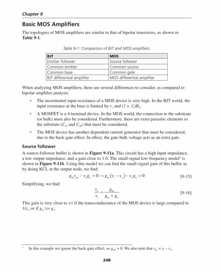
Chapter 9
248
Basic MOS Amplifi ersThe topologies of MOS amplifi ers are similar to that of bipolar transistors, as shown in Table 9-1.
Table 9-1: Comparison of BJT and MOS amplifi ers.
BJT MOSEmitter follower Source followerCommon emitter Common sourceCommon base Common gateBJT differential amplifi er MOS differential amplifi er
When analyzing MOS amplifi ers, there are several differences to consider, as compared to bipolar amplifi er analysis:
• The incremental input resistance of a MOS device is very high. In the BJT world, the input resistance at the base is limited by rπ and (1 + βo)RE.
• A MOSFET is a 4-terminal device. In the MOS world, the connection to the substrate (or bulk) must also be considered. Furthermore, there are extra parasitic elements to the substrate (Csb and Cdb) that must be considered.
• The MOS device has another dependent current generator that must be considered, due to the back-gate effect. In effect, the gate-bulk voltage acts as an extra gate.
Source followerA source-follower buffer is shown in Figure 9-11a. This circuit has a high input impedance, a low output impedance, and a gain close to 1.0. The small-signal low-frequency model7 is shown in Figure 9-11b. Using this model we can fi nd the small-signal gain of this buffer as by doing KCL at the output node, we fi nd:
( )0 0m gs o o m i o o og v v g g v v v g− = → − − = [9-15]
Simplifying, we fi nd:
o m
i m o
v g
v g g=
+ [9-16]
This gain is very close to +1 if the transconductance of the MOS device is large compared to 1/ro, or if gm >> go.
7 In this example we ignore the back-gate effect, so gmb = 0. We also note that vgs = vi – vo.
Thompson Book.indb 248 3/20/2006 11:35:44 AM
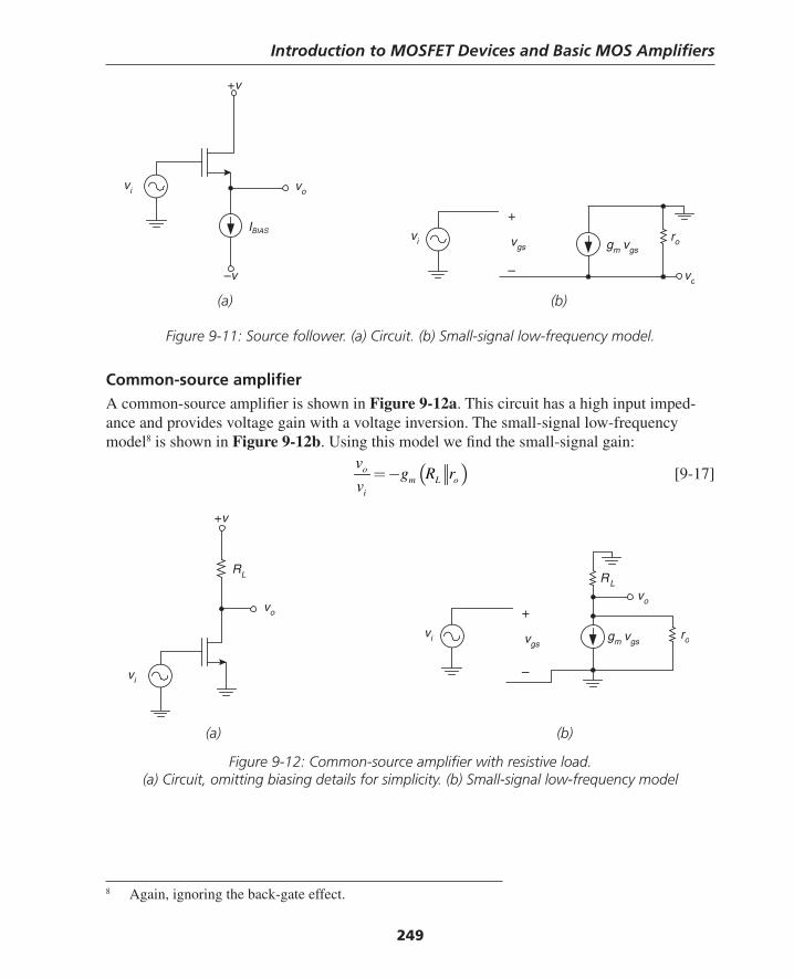
Introduction to MOSFET Devices and Basic MOS Amplifi ers
249
(a) (b)
Figure 9-11: Source follower. (a) Circuit. (b) Small-signal low-frequency model.
Common-source amplifi erA common-source amplifi er is shown in Figure 9-12a. This circuit has a high input imped-ance and provides voltage gain with a voltage inversion. The small-signal low-frequency model8 is shown in Figure 9-12b. Using this model we fi nd the small-signal gain:
( )om L o
i
vg R r
v= − [9-17]
gm vgs
ro
vo
vgs
+
–
vi
vi vo
+v
–v
IBIAS
8 Again, ignoring the back-gate effect.
(a) (b)
Figure 9-12: Common-source amplifi er with resistive load. (a) Circuit, omitting biasing details for simplicity. (b) Small-signal low-frequency model
gm vgsro
vo
vgs
+
–
vi
vi
vo
+v
RL RL
Thompson Book.indb 249 3/20/2006 11:35:45 AM
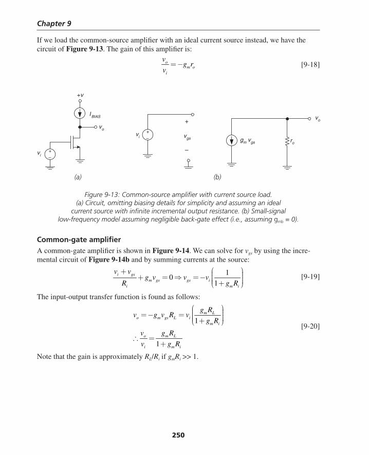
Chapter 9
250
If we load the common-source amplifi er with an ideal current source instead, we have the circuit of Figure 9-13. The gain of this amplifi er is:
om o
i
vg r
v= − [9-18]
(a) (b)
Figure 9-13: Common-source amplifi er with current source load. (a) Circuit, omitting biasing details for simplicity and assuming an ideal
current source with infi nite incremental output resistance. (b) Small-signal low-frequency model assuming negligible back-gate effect (i.e., assuming gmb = 0).
Common-gate amplifi erA common-gate amplifi er is shown in Figure 9-14. We can solve for vgs by using the incre-mental circuit of Figure 9-14b and by summing currents at the source:
10
1i gs
m gs gs ii m i
v vg v v v
R g R
⎛ ⎞+ ⎟⎜ ⎟+ = ⇒ = − ⎜ ⎟⎜ ⎟⎜ +⎝ ⎠ [9-19]
The input-output transfer function is found as follows:
1
1
m Lo m gs L i
m i
o m L
i m i
g Rv g v R v
g R
v g R
v g R
⎛ ⎞⎟⎜ ⎟= − = ⎜ ⎟⎜ ⎟⎜ +⎝ ⎠
∴ =+
[9-20]
Note that the gain is approximately RL/Ri if gmRi >> 1.
gm vgs ro
vo+
–vi
+v
vgs
vo
IBIAS
+–
+–
vi
Thompson Book.indb 250 3/20/2006 11:35:45 AM
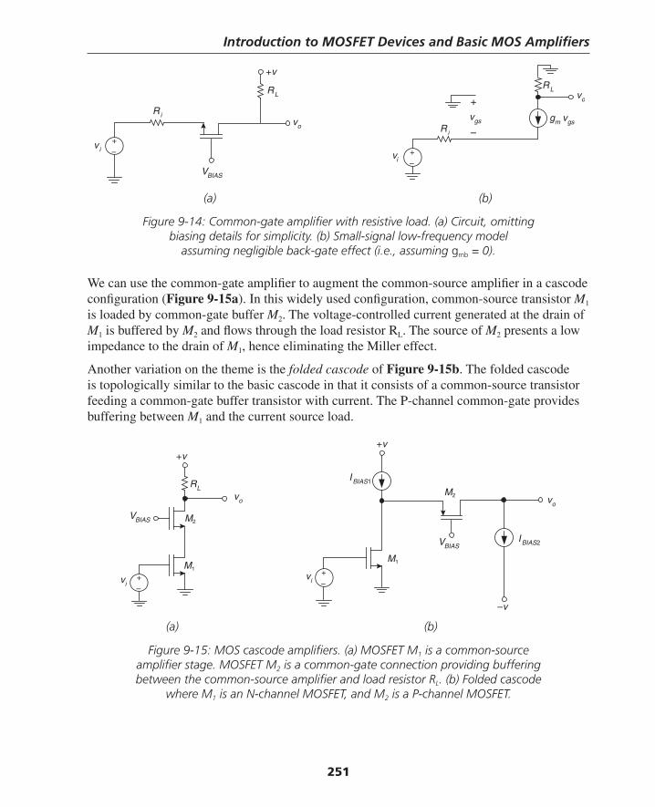
Introduction to MOSFET Devices and Basic MOS Amplifi ers
251
(a) (b)
Figure 9-14: Common-gate amplifi er with resistive load. (a) Circuit, omitting biasing details for simplicity. (b) Small-signal low-frequency model
assuming negligible back-gate effect (i.e., assuming gmb = 0).
We can use the common-gate amplifi er to augment the common-source amplifi er in a cascode confi guration (Figure 9-15a). In this widely used confi guration, common-source transistor M1 is loaded by common-gate buffer M2. The voltage-controlled current generated at the drain of M1 is buffered by M2 and fl ows through the load resistor RL. The source of M2 presents a low impedance to the drain of M1, hence eliminating the Miller effect.
Another variation on the theme is the folded cascode of Figure 9-15b. The folded cascode is topologically similar to the basic cascode in that it consists of a common-source transistor feeding a common-gate buffer transistor with current. The P-channel common-gate provides buffering between M1 and the current source load.
gm vgs
Ri
vo
+v
VBIAS
+–
+
–
vgsvo Ri
RLRL
vi
vi +–
VBIAS
vo
+v
VBIAS
+v
IBIAS2
I BIAS1
M1
M2
M1
M2vo
vi
RL
vi
–v
+–
+–
(a) (b)
Figure 9-15: MOS cascode amplifi ers. (a) MOSFET M1 is a common-source amplifi er stage. MOSFET M2 is a common-gate connection providing buffering between the common-source amplifi er and load resistor RL. (b) Folded cascode
where M1 is an N-channel MOSFET, and M2 is a P-channel MOSFET.
Thompson Book.indb 251 3/20/2006 11:35:45 AM
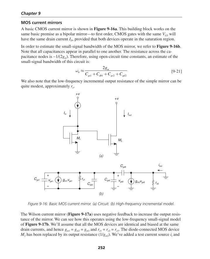
Chapter 9
252
MOS current mirrorsA basic CMOS current mirror is shown in Figure 9-16a. This building block works on the same basic premise as a bipolar mirror—to fi rst order, CMOS gates with the same VGS will have the same drain current ID, provided that both devices operate in the saturation region.
In order to estimate the small-signal bandwidth of the MOS mirror, we refer to Figure 9-16b. Note that all capacitances appear in parallel to one another. The resistance across the ca-pacitance nodes is ∼1/(2gm). Therefore, using open-circuit time constants, an estimate of the small-signal bandwidth of this circuit is:
1 1 2 2
2 mh
gs db gs gd
g
C C C Cω ≈
+ + + [9-21]
We also note that the low-frequency incremental output resistance of the simple mirror can be quite modest, approximately ro.
(a)
+v
Iin Iout
M1 M2
Cgs1 Cgs2vgs1 gm1vgs1 vgs2 gm2vgs2
Cgd2
Cdb1
iout
+
–ro2
ro1
+
–
+v
(b)
Figure 9-16: Basic MOS current mirror. (a) Circuit. (b) High-frequency incremental model.
The Wilson current mirror (Figure 9-17a) uses negative feedback to increase the output resis-tance of the mirror. We can see how this operates using the low-frequency small-signal model of Figure 9-17b. We’ll assume that all the MOS devices are identical and biased at the same drain currents, and hence gm1 = gm2 = gm3 and ro1 = ro2 = ro3. The diode-connected MOS device M2 has been replaced by its output resistance (1/gm2). We’ve added a test current source it and
Thompson Book.indb 252 3/20/2006 11:35:46 AM
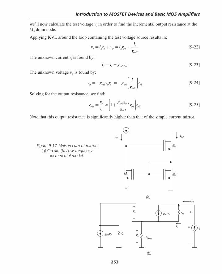
Introduction to MOSFET Devices and Basic MOS Amplifi ers
253
we’ll now calculate the test voltage vt in order to fi nd the incremental output resistance at the M3 drain node.
Applying KVL around the loop containing the test voltage source results in:
32
tt x o b x o
m
iv i r v i r
g= + = + [9-22]
The unknown current ix is found by:
3x t m ai i g v= − [9-23]
The unknown voltage va is found by:
1 1 1 12
ta m b o m o
m
iv g v r g r
g
⎛ ⎞⎟⎜ ⎟= − = − ⎜ ⎟⎜ ⎟⎜⎝ ⎠ [9-24]
Solving for the output resistance, we fi nd:
1 31 3
2
1t m mout o o
t m
v g gr r r
i g
⎛ ⎞⎟⎜ ⎟= ≈ +⎜ ⎟⎜ ⎟⎜⎝ ⎠ [9-25]
Note that this output resistance is signifi cantly higher than that of the simple current mirror.
(a)
va
gm1vb
+
–
ro1
Iout
M2
rout
M3
Iin
M1
vb
+
–
ro3+
–
vt it
gm3va
gm21/
ix
(b)
Figure 9-17. Wilson current mirror. (a) Circuit. (b) Low-frequency
incremental model.
Thompson Book.indb 253 3/20/2006 11:35:46 AM
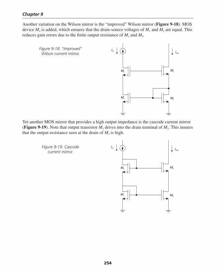
Chapter 9
254
Figure 9-18: “Improved” Wilson current mirror.
Yet another MOS mirror that provides a high output impedance is the cascode current mirror (Figure 9-19). Note that output transistor M3 drives into the drain terminal of M2. This insures that the output resistance seen at the drain of M3 is high.
Figure 9-19: Cascode current mirror.
Iout
M2
M3
Iin
M1
M4
Iout
M2
M3
Iin
M1
M4
Another variation on the Wilson mirror is the “improved” Wilson mirror (Figure 9-18). MOS device M4 is added, which ensures that the drain-source voltages of M1 and M2 are equal. This reduces gain errors due to the fi nite output resistance of M1 and M2.
Thompson Book.indb 254 3/20/2006 11:35:47 AM
Introduction to MOSFET Devices and Basic MOS Amplifi ers
255
Example 9.1: MOS amplifi er design exampleLet’s work out a MOS design example illustrating the use of MOS models and open-circuit time constants for bandwidth analysis. Let’s assume that we need a gain magnitude of 10 (i.e., 20dB) and a –3dB bandwidth in excess of 350 MHz. The input source has a series resistance of 1 kΩ and that the amplifi er drives a 1-picofarad load capacitance. Ignore the back gate effect (i.e., assume that gmb = 0). Assume that the bulk (i.e., substrate) connections of the tran-sistors are tied to ground. The MOS transistors have the following parameters:
• gm = 0.01 A/V
• ro = 3 kΩ
• Gate-source capacitance Cgs = 0.2 pF
• Gate-drain capacitance Cgd = 0.05 pF
• Source-substrate capacitance Csb = 0.02 pF
• Drain-substrate capacitance Cdb = 0.02 pF
TRY #1: Common-source amplifi erA fi rst-cut design for this amplifi er is shown in Figure 9-20a, with low-frequency small-sig-nal model shown in Figure 9-20b. We can use the low-frequency small-signal model to fi nd the minimum value of the load resistor RL in order to meet the gain specifi cation, as follows:
1500om L o L
i
vg R r R
v= − ⇒ > Ω [9-26]
We’ll use RL = 1.6 kΩ so that there’s a little bit of extra gain, and also to account for the fact that we’ve ignored the back-gate effect.
We’ll fi nd the bandwidth using the high-frequency small-signal model of Figure 9-20c. Note that the load (CL) and drain-substrate (Cdb) capacitances are in parallel. The source-substrate (Csb) capacitance is not included since the source and substrate are both incrementally grounded.
Thompson Book.indb 255 3/20/2006 11:35:47 AM
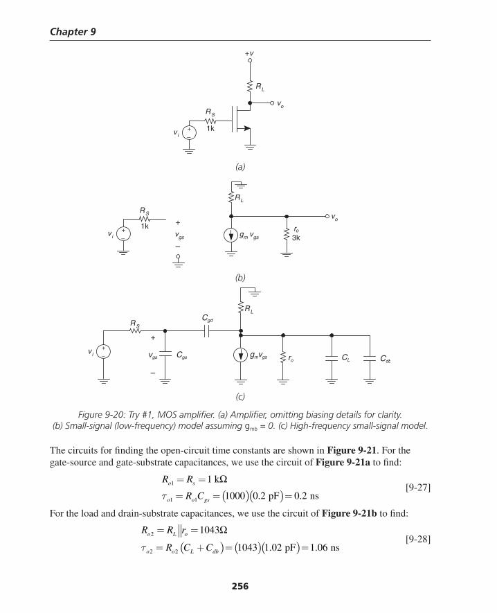
Chapter 9
256
(a)
+v
RS
+–
vi
vo
RL
1k
RL
vo
RS
+–
vi
1k +
–
vgs gm vgs 3kro
Cgs CLvgs gmvgs
Cgd
Cdbro
RS
+–
vi
RL
+
–
(b)
(c)
Figure 9-20: Try #1, MOS amplifi er. (a) Amplifi er, omitting biasing details for clarity. (b) Small-signal (low-frequency) model assuming gmb = 0. (c) High-frequency small-signal model.
The circuits for fi nding the open-circuit time constants are shown in Figure 9-21. For the gate-source and gate-substrate capacitances, we use the circuit of Figure 9-21a to fi nd:
( )( )
1
1 1
1 k
1000 0.2 pF 0.2 nso s
o o gs
R R
R Cτ
= =
= = =
Ω [9-27]
For the load and drain-substrate capacitances, we use the circuit of Figure 9-21b to fi nd:
( ) ( )( )
2
2 2
1043
1043 1.02 pF 1.06 ns
o L o
o o L db
R R r
R C Cτ
= =
= + = =
Ω [9-28]
Thompson Book.indb 256 3/20/2006 11:35:47 AM
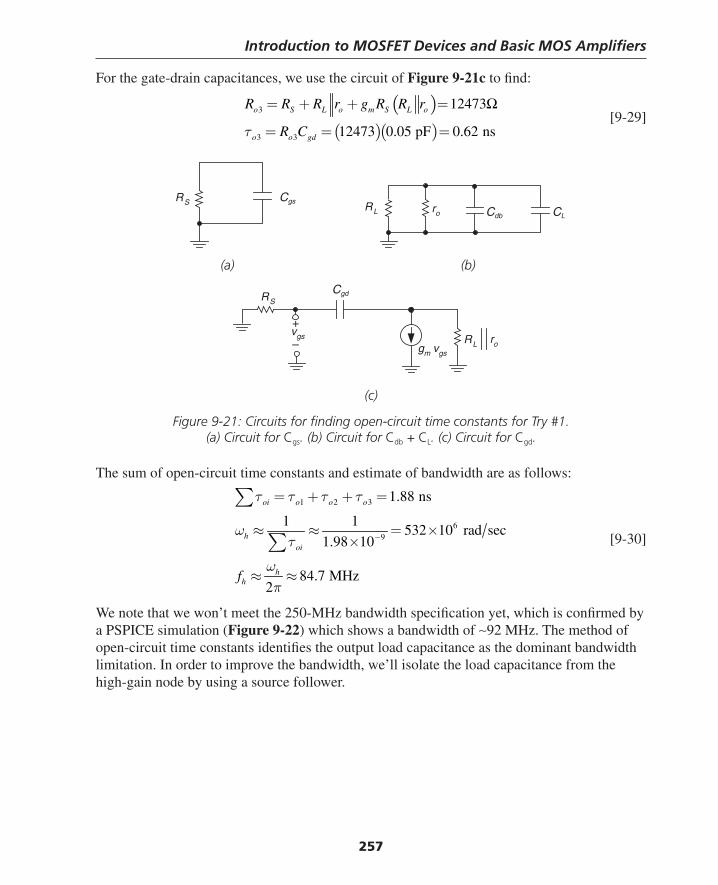
Introduction to MOSFET Devices and Basic MOS Amplifi ers
257
For the gate-drain capacitances, we use the circuit of Figure 9-21c to fi nd:
( )
( )( )3
3 3
12473
12473 0.05 pF 0.62 ns
o S L o m S L o
o o gd
R R R r g R R r
R Cτ
= + + =
= = =
Ω [9-29]
(a) (b)
CgsRS
CLCdbRL ro
RS
vgs
gm vgs
Cgd
+
– RL ro
(c)
Figure 9-21: Circuits for fi nding open-circuit time constants for Try #1. (a) Circuit for Cgs. (b) Circuit for Cdb + CL. (c) Circuit for Cgd.
The sum of open-circuit time constants and estimate of bandwidth are as follows:
1 2 3
69
1.88 ns
1 1532 10 rad sec
1.98 10
84.7 MHz2
oi o o o
hoi
hhf
τ τ τ τ
ωτ
ωπ
−
= + + =
≈ ≈ = ××
≈ ≈
∑
∑ [9-30]
We note that we won’t meet the 250-MHz bandwidth specifi cation yet, which is confi rmed by a PSPICE simulation (Figure 9-22) which shows a bandwidth of ∼92 MHz. The method of open-circuit time constants identifi es the output load capacitance as the dominant bandwidth limitation. In order to improve the bandwidth, we’ll isolate the load capacitance from the high-gain node by using a source follower.
Thompson Book.indb 257 3/20/2006 11:35:48 AM
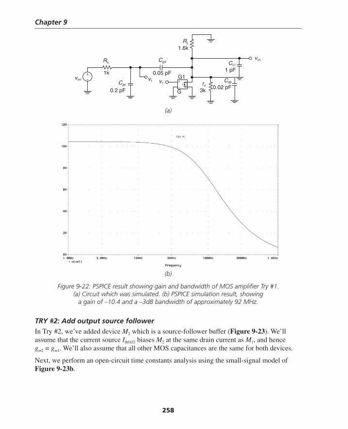
Chapter 9
258
(a)
+–vin1
Rs
1k
Cgs
0.2 pF
Cgd
0.05 pF
RL
1.6k
CL1
1 pF
Cdb
0.02 pFro
3k
v1 v1
G1
G
+
–
vo1
(b)
Figure 9-22: PSPICE result showing gain and bandwidth of MOS amplifi er Try #1. (a) Circuit which was simulated. (b) PSPICE simulation result, showing
a gain of –10.4 and a –3dB bandwidth of approximately 92 MHz.
TRY #2: Add output source followerIn Try #2, we’ve added device M2 which is a source-follower buffer (Figure 9-23). We’ll assume that the current source IBIAS2 biases M2 at the same drain current as M1, and hence gm2 = gm1. We’ll also assume that all other MOS capacitances are the same for both devices.
Next, we perform an open-circuit time constants analysis using the small-signal model of Figure 9-23b.
Thompson Book.indb 258 3/20/2006 11:35:48 AM
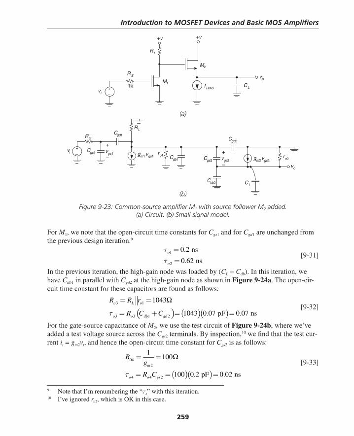
Introduction to MOSFET Devices and Basic MOS Amplifi ers
259
(a)
vo
IBIAS
+v
M1
vi
1k+–
RL
+v
M2
RS
CL
gm1vgs1+
–
RS
vo
+–
RL
CL
gm2vgs2ro2
ro1 Cdb1
Cgd2
Cgd1
Cgs1vi vgs1
Cgs2 vgs2
Csb2
+
–
(b)
Figure 9-23: Common-source amplifi er M1 with source follower M2 added. (a) Circuit. (b) Small-signal model.
For M1, we note that the open-circuit time constants for Cgs1 and for Cgd1 are unchanged from the previous design iteration.9
1
2
0.2 ns
0.62 nso
o
τ
τ
=
= [9-31]
In the previous iteration, the high-gain node was loaded by (CL + Cdb). In this iteration, we have Cdb1 in parallel with Cgd2 at the high-gain node as shown in Figure 9-24a. The open-cir-cuit time constant for these capacitors are found as follows:
( ) ( )( )
3 1
3 3 1 2
1043
1043 0.07 pF 0.07 ns
o L o
o o db gd
R R r
R C Cτ
= =
= + = =
Ω [9-32]
For the gate-source capacitance of M2, we use the test circuit of Figure 9-24b, where we’ve added a test voltage source across the Cgs2 terminals. By inspection,10 we fi nd that the test cur-rent it = gm2vt, and hence the open-circuit time constant for Cgs2 is as follows:
( )( )
042
4 4 2
1100
100 0.2 pF 0.02 nsm
o o gs
Rg
R Cτ
= =
= = =
Ω [9-33]
9 Note that I’m renumbering the “τs” with this iteration.10 I’ve ignored ro2, which is OK in this case.
Thompson Book.indb 259 3/20/2006 11:35:49 AM
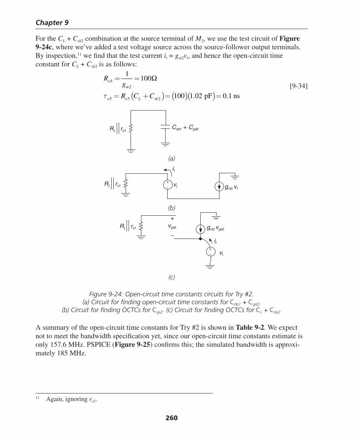
Chapter 9
260
For the CL + Csb2 combination at the source terminal of M2, we use the test circuit of Figure 9-24c, where we’ve added a test voltage source across the source-follower output terminals. By inspection,11 we fi nd that the test current it = gm2vt, and hence the open-circuit time constant for CL + Csb2 is as follows:
( ) ( )( )
52
5 5 2
1100
100 1.02 pF 0.1 ns
om
o o L sb
Rg
R C Cτ
= =
= + = =
Ω [9-34]
11 Again, ignoring ro2.
(a)
Cdb1 + Cgd2RL ro1
vtRL ro1+–
it
gm2 vt
+
–
vt
RL ro1
it
gm2 vgs2vgs2
+–
(b)
(c)
Figure 9-24: Open-circuit time constants circuits for Try #2. (a) Circuit for fi nding open-circuit time constants for Cdb1 + Cgd2.
(b) Circuit for fi nding OCTCs for Cgs2. (c) Circuit for fi nding OCTCs for CL + Csb2.
A summary of the open-circuit time constants for Try #2 is shown in Table 9-2. We expect not to meet the bandwidth specifi cation yet, since our open-circuit time constants estimate is only 157.6 MHz. PSPICE (Figure 9-25) confi rms this; the simulated bandwidth is approxi-mately 185 MHz.
Thompson Book.indb 260 3/20/2006 11:35:49 AM
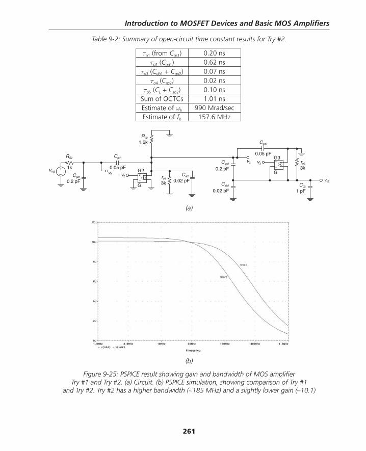
Introduction to MOSFET Devices and Basic MOS Amplifi ers
261
Table 9-2: Summary of open-circuit time constant results for Try #2.
τo1 (from Cgs1) 0.20 nsτo2 (Cgd1) 0.62 ns
τo3 (Cdb1 + Cgd2) 0.07 nsτo4 (Cgs2) 0.02 ns
τo5 (CL + Csb2) 0.10 nsSum of OCTCs 1.01 nsEstimate of ωh 990 Mrad/secEstimate of fh 157.6 MHz
(a)
+–
vin2
Cgd1
0.05 pF
RL2
1.6k
CL2
1 pF
Cdb1
0.02 pFro1
3k
v2 v2
G2
G
+
–Cgs1
0.2 pF
1k
RS2
Cgd2
0.05 pF
v3 v3
G3
G
ro2
3k
vo2
+
–Cgs2
0.2 pF
Csb2
0.02 pF
(b)
Figure 9-25: PSPICE result showing gain and bandwidth of MOS amplifi er Try #1 and Try #2. (a) Circuit. (b) PSPICE simulation, showing comparison of Try #1
and Try #2. Try #2 has a higher bandwidth (∼185 MHz) and a slightly lower gain (–10.1)
Thompson Book.indb 261 3/20/2006 11:35:50 AM
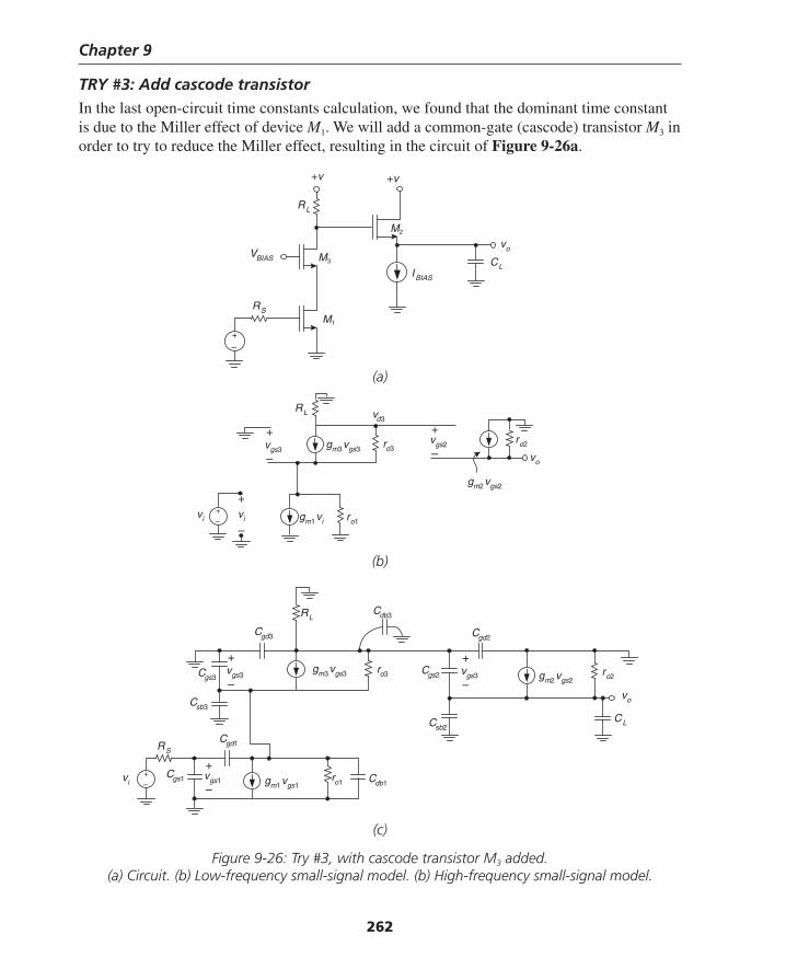
Chapter 9
262
TRY #3: Add cascode transistorIn the last open-circuit time constants calculation, we found that the dominant time constant is due to the Miller effect of device M1. We will add a common-gate (cascode) transistor M3 in order to try to reduce the Miller effect, resulting in the circuit of Figure 9-26a.
vo
IBIAS
+v
M1
M3
+–
RL
+v
M2
RS
CL
VBIAS
+
–vgs2
+
–vgs3
gm3vgs3
gm1vi
ro2ro3
ro1
RL
+
–vivi
vo
vd3
gm2vgs2
+–
gm3vgs3
gm1vgs1
gm2vgs2
RL
ro2ro3
CL
RS
vi
+
–vgs3
+
–vgs1
Cgd2Cgd3
Cgs2
Csb2
Cgs1
Cgd1
Cgs3
Csb3
ro1 Cdb1
Cdb3
vo
+–
+
–vgs3
(a)
(b)
(c)
Figure 9-26: Try #3, with cascode transistor M3 added. (a) Circuit. (b) Low-frequency small-signal model. (b) High-frequency small-signal model.
Thompson Book.indb 262 3/20/2006 11:35:51 AM

Introduction to MOSFET Devices and Basic MOS Amplifi ers
263
The low-frequency small-signal model is shown in Figure 9-26b. We note from this model that the gain of this amplifi er confi guration is now roughly:
v
vg Ro
im L≈ − 1 [9-35]
This assumes that the loading effect of ro3 is minimized at the high-gain node and that the gain of the M3 emitter-follower is close to unity. We can argue that ro3 doesn’t signifi cantly affect the gain by noting that the incremental output resistance seen at the drain of M3 is increased due to the fact that the source of M3 is loaded with a relatively high resistance (i.e., ro1). Thus, the effects of loading due to the output resistance ro3 is minimized. We can then reduce the load resistor in this iteration to perhaps 1.1 kΩ (reduced from 1.6 kΩ) and still meet the gain specifi cation. This will also help us meet the bandwidth specifi cation.
Referring to the small-signal circuit of Figure 9-26c, we now need to do some bookkeep-ing to keep track of all the various capacitances and open-circuit time constant calculations. There are 13 capacitances that contribute to open-circuit time constants: four for each transis-tor plus the load capacitance. However, we fi nd that some capacitances are shorted out since all transistors have the bulk terminal grounded (i.e., Csb1 and Cdb2) and that there are many capacitances that are in parallel (i.e., Cdb1 + Cgs3 + Csb3; Csb2 + CL; and Cgd2 + Cgd3 + Cdb3). The open-circuit time constant calculations for the various capacitances are shown in Table 9-2.
Table 9-2: Summary of OCTC calculations for Try #3.
Capacitance(s) Open-circuit resistanceOpen-circuit time constant calculation
Cgs1 = 0.2 pFUnchanged from previous iteration at 1 kΩ τo1 unchanged at 0.2 ns
Cgd1 = 0.05 pF
Open-circuit resistance is greatly reduced due to low output resistance ≈ rout3 = 100Ω at source of M3. Ro2 = Rs + rout3 + gm1Rsrout3 = 2100Ω
τo2 = (2100)(0.05 pF) = 0.105 ns
Cdb1 + Csb3 + Cgs3 = 0.24 pF
Open-circuit resistance = rout3 ≈ 1/gm3 = 100Ω τo3 = (100)(0.24 pF) = 0.024 ns
Cgs2 = 0.2 pFOpen-circuit resistance unchanged at 1/gm2 = 100Ω τo4 = (100)(0.2 pF) = 0.02 ns
Cgd2 + Cdb3 + Cgd3 = 0.12 pF
Resistance from this common node to ground ≈ RL = 1100Ω τo5 =(1100)(0.12 pF) = 0.132 ns
Csb2 + CL = 1.02 pF Open-circuit resistance = 1/gm2 = 100Ω τo5 =(100)(1.02 pF) = 0.10 ns
The sum of the open-circuit time constants is now 0.58 nanoseconds, resulting in a bandwidth estimate of 1721 Mrad/seconds, or 274 MHz. This circuit looks like a good candidate for fi nal simulation, since we know the method of open-circuit time constants is always conservative in estimating bandwidth. A detailed PSPICE simulation shows that the bandwidth is 460 MHz (Figure 9-27), and hence we meet our 350 MHz bandwidth specifi cation.
Thompson Book.indb 263 3/20/2006 11:35:51 AM
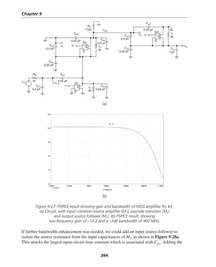
Chapter 9
264
(a)
+–
vin3
Cgd1
0.05 pF
Cdb1
0.02 pFro1
3k
v4
G1
G
+
–Cgs1
0.2 pF
1k
RS2
RL2
1100G3
G
+–
v6
G2
G
+
–v6
vhigh
v4
CSb3
0.02 pF
Cgs3
0.2 pF
Cgd3
0.05 pF Cdb3
0.02 pFro3
3k
Cgs2
0.2 pF
Csb2
0.02 pF
Cgd2
0.05 pF
v5 v5ro2
3k
CL2
1 pF
vo3
(b)
Figure 9-27: PSPICE result showing gain and bandwidth of MOS amplifi er Try #3.(a) Circuit, with input common-source amplifi er (M1), cascode transistor (M3)
and output source follower (M2). (b) PSPICE result, showing low-frequency gain of –10.2 and a –3dB bandwidth of 460 MHz.
If further bandwidth enhancement was needed, we could add an input source-follower to isolate the source resistance from the input capacitances of M1, as shown in Figure 9-28a. This attacks the largest open-circuit time constant which is associated with Cgs1. Adding the
Thompson Book.indb 264 3/20/2006 11:35:51 AM
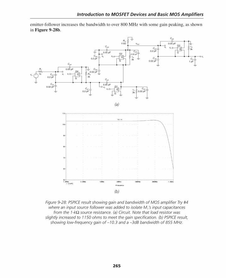
Introduction to MOSFET Devices and Basic MOS Amplifi ers
265
emitter-follower increases the bandwidth to over 800 MHz with some gain peaking, as shown in Figure 9-28b.
(a)
+–
vin
Cgd1
0.05 pF
Cdb1
0.02 pFro1
3k
v4
G1
G
+Cgs1
0.2 pF
1k Ro4
3k
RL2
1150G3
G
+–
v6
G2
G
+
–v6
vhigh
v4
CSb3
0.02 pF
Cgs3
0.2 pF
Cgd3
0.05 pF Cdb3
0.02 pFro3
3k
Cgs2
0.2 pF
Csb2
0.02 pF
Cgd2
0.05 pF
v5 v5ro2
3k
CL2
1 pF
vo
–
Cgd4
0.05 pF
v7
G4
G
+v7–
Cgs4
0.2 pF
Csb4
0.02 pF
Rs
(b)
Figure 9-28: PSPICE result showing gain and bandwidth of MOS amplifi er Try #4 where an input source follower was added to isolate M1’s input capacitances
from the 1-kΩ source resistance. (a) Circuit. Note that load resistor was slightly increased to 1150 ohms to meet the gain specifi cation. (b) PSPICE result,
showing low-frequency gain of –10.3 and a –3dB bandwidth of 855 MHz.
Thompson Book.indb 265 3/20/2006 11:35:52 AM
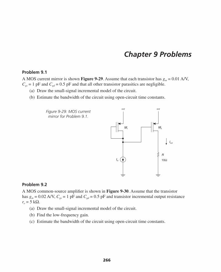
266
Chapter 9 Problems
Problem 9.1A MOS current mirror is shown Figure 9-29. Assume that each transistor has gm = 0.01 A/V, Cgs = 1 pF and Cgd = 0.5 pF and that all other transistor parasitics are negligible.
(a) Draw the small-signal incremental model of the circuit.
(b) Estimate the bandwidth of the circuit using open-circuit time constants.
Problem 9.2A MOS common-source amplifi er is shown in Figure 9-30. Assume that the transistor has gm = 0.02 A/V, Cgs = 1 pF and Cgd = 0.5 pF and transistor incremental output resistance ro = 5 kΩ.
(a) Draw the small-signal incremental model of the circuit.
(b) Find the low-frequency gain.
(c) Estimate the bandwidth of the circuit using open-circuit time constants.
+v +v
R
10ΩIin
Iout
M1 M2
Figure 9-29: MOS current mirror for Problem 9.1.
Thompson Book.indb 266 3/20/2006 11:35:53 AM
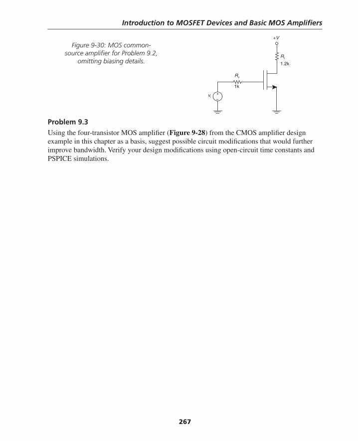
Introduction to MOSFET Devices and Basic MOS Amplifi ers
267
Problem 9.3Using the four-transistor MOS amplifi er (Figure 9-28) from the CMOS amplifi er design example in this chapter as a basis, suggest possible circuit modifi cations that would further improve bandwidth. Verify your design modifi cations using open-circuit time constants and PSPICE simulations.
+–
vi
Rs
1k
RL
1.2k
+V
Figure 9-30: MOS common-source amplifi er for Problem 9.2,
omitting biasing details.
Thompson Book.indb 267 3/20/2006 11:35:53 AM

Chapter 9
268
ReferencesArns, R. G., “The other transistor: early history of the metal-oxide semiconductor fi eld-effect
transistor,” Engineering Science and Education Journal, vol. 7, no. 5, October 1998, pp. 233–240.
Comer, David J., and Comer, Donald T., “Teaching MOS Integrated Circuit Amplifi er Design to Undergraduates,” IEEE Transactions on Education, vol. 44, no. 3, August 2001, pp. 232– 238.
Gray, P. R., and Meyer, R. G., “MOS operational amplifi er design-a tutorial overview,” IEEE Journal of Solid State Circuits, vol. 17, no. 6, December 1982, pp. 969–982.
Grebene, Alan B., Bipolar and MOS Analog Integrated Circuits, John Wiley, 1984.Hastings, Alan, The Art of Analog Layout, Prentice Hall, 2001.Hodges, D. A., Gray, P. R., and Brodersen, R. W., “Potential of MOS technologies for analog
integrated circuits,” IEEE Journal of Solid State Circuits, vol. 13, no. 3, June 1978, pp. 285–294.
Jiang, Ruoxin, Tang, Haiming, and Mayaram, Kartikeya, “A Simple and Accurate Method for Calculating the Low Frequency Common-Mode Gain in a MOS Differential Amplifi er with a Current-Mirror Load,” IEEE Transactions on Education, vol. 43, no. 3, August 2000, pp. 362–364.
Johns, David A., and Martin, Ken, Analog Integrated Circuit Design, John Wiley, 1997.Lee, Thomas H., The Design of CMOS Radio-Frequency Integrated Circuits, Cambridge
University Press, 1998.Lilienfeld J., US Patents 1,745, 175; 1,877, 140 and 1,900,018, available from the U.S. Patent
and Trademark offi ce, www.uspto.gov.Middlebrook, R. D., and Richer, I., “Limits on the Power-Law Exponent for Field-Effect
Transistor Transfer Characteristics,” Solid-State Electronics, vol. 6, September-October 1963, pp. 542–544.
Pierret, Robert F., Modular Series on Solid State Devices, Field Effect Devices, (volume 4), Addison-Wesley, 1983. Singh, Jasprit, Semiconductor Devices Basic Principles, John Wiley, 2001.
Sze, S. M., Semiconductor Devices Physics and Technology, 2nd edition, John Wiley, 2002.Winarski, T. Y., “Dielectrics in MOS devices, DRAM capacitors, and inter-metal isolation,”
IEEE Electrical Insulation Magazine, vol. 17, no. 6, November-December 2001, pp. 34–47.
Thompson Book.indb 268 3/20/2006 11:35:53 AM
269
C H A P T E R 10Bipolar Transistor Switching
and the Charge Control Model
IntroductionIn previous chapters, we discussed the dynamic behavior of transistors from a small-signal point of view using the hybrid-pi model. In other words, the small-signal models developed so far are valid only for small variations of the voltages and currents around an operating point. We used the method of open-circuit time constants to analyze bandwidth limitations in linear amplifi ers.
A further modeling technique, called the charge control model, permits us to analyze the behavior of transistor circuits during large-signal switching and during transistor saturation. Similarly to the method of open-circuit time constants, the charge control model gives results that aren’t necessarily numerically accurate; rather the usefulness of the method is the design insight that we derive from the application of relatively simple models.
Development of the Switching ModelsIn the following development, we consider the charge control model for the NPN transistor. The results are exactly the same for a PNP transistor. Transistor terminal current defi nitions are given in Figure 10-1.
In This Chapter
In this chapter, we examine in detail large-signal switching of bipolar transistors. A model used to the switching speed, called the charge control model, is introduced.
Figure 10-1: Terminal defi nitions for NPN transistor, showing base current ib, collector current ic and emitter current ie.
ib
ie
ic
Thompson Book.indb 269 3/20/2006 11:35:54 AM
Chapter 10
270
From device physics, we derived in an earlier chapter the fact that when a transistor is biased in the forward-active region the base-to-emitter junction is forward biased and there is extra charge stored in the base region. For an NPN transistor, the excess minority carrier con-centration is shown in Figure 10-2. In the case of the NPN transistor, the base is made of P material and the excess minority carriers are electrons, and have the profi le n(x) shown. There is a similar hole profi le in the emitter p(x) but for purposes of analyzing switching operation we need only consider the base region.
Since transistor collector current is dominated by diffusion in the base, collector current Ic is proportional to the slope of the n'(x) curve. The dotted line shows the carrier concentration profi le at a higher collector current. Since the vertical axis has units of charge concentration, the total area under the curve is proportional to the charge stored in the base of the transis-tor. When the transistor is operated in the normal fashion and in the linear region (called the forward-active region) we’ll call this stored charge qF, for forward charge.
We can summarize this relationship between collector current and the charge stored in the base as:
Fc
F
qi
τ= [10-1]
where τF is a device-dependent constant that has units of time. This is the charge-control equation for the collector current in the forward-active region. We assume that as the base-emitter voltage changes, the concentration n'(x = 0) changes instantaneously in response.1
Now, we need to consider the base current. Since there is charge stored in the base, we expect that the base current charge control equation has a term related to how fast we add and re-move charge qF from the base. Furthermore, we know that there has to be a DC term (because collector and base current bias levels are related by the large signal βF). Using this reasoning, the base current charge control equation is:
F Fb
BF
q dqi
dtτ= + [10-2]
xqF
Ic
n'(x)n'(x) athigher
NEmitter
PBase
NCollector
1 This is approximately true as long as we don’t allow the transistor vbe to change too fast.
Figure 10-2: Excess carrier concentration for NPN
transistor in forward-active region. The extra charge in the base (n‘(x)) causes a net diffusion current of electrons
to the right, resulting in a collector current to the left.
Thompson Book.indb 270 3/20/2006 11:35:54 AM
Bipolar Transistor Switching and the Charge Control Model
271
The qF/τBF term is the DC base current, and the dqF/dt term is the charge needed if we change the charge stored in the base. The characteristic time τBF is related to τF in a way that we’ll explain later.
We also recognize that the emitter current is the negative sum of the collector and base currents, or:
( )e c bi i i= − + [10-3]
Summarizing, the charge control equations for the forward-active region are:
( )
F Fb
BF
Fc
F
e c b
q dqi
dt
qi
i i i
τ
τ
= +
=
= − +
[10-4]
Note that these equations do not account for charge stored in the base-emitter and base-col-lector junction capacitances. We’ll fi x this later.
Reverse-Active RegionIn the forward-active region, the base-emitter junction is forward biased and the collector-base junction is reverse biased. We could just as easily operate the transistor with the collector-base junction forward biased, and the base-emitter junction reverse biased. This mode of operation is called the reverse-active region, and analysis is exactly analogous with the forward-active region, with the roles of the collector and emitter reversed.2 The carrier profi le is as shown in Figure 10-3. The charge control equations in the reverse-active region are:
( )
R Rb
BR
Re
R
c e b
q dqi
dt
qi
i i i
τ
τ
= +
=
= − +
[10-5]
n'(x)
NEmitter
PBase
NCollector
xqR
Figure 10-3: Excess carrier concentration for NPN transistor
in reverse-active region. Note that in the reverse-active region the
collector-base junction is forward biased and the base-emitter junction is reverse biased.
2 The charge stored in the base in the reverse-active region is qR.
Thompson Book.indb 271 3/20/2006 11:35:55 AM
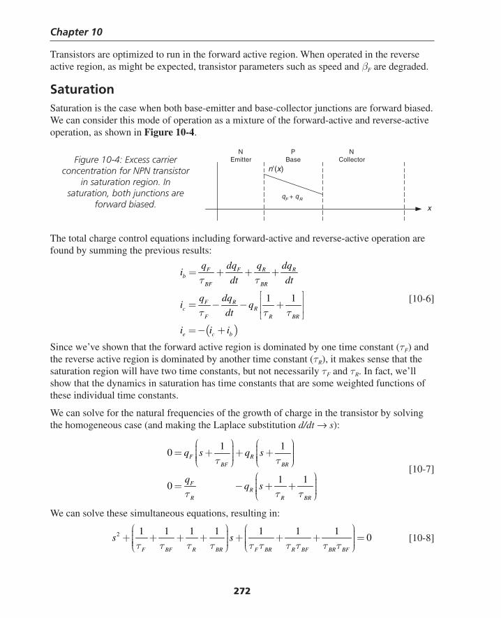
Chapter 10
272
Transistors are optimized to run in the forward active region. When operated in the reverse active region, as might be expected, transistor parameters such as speed and βF are degraded.
SaturationSaturation is the case when both base-emitter and base-collector junctions are forward biased. We can consider this mode of operation as a mixture of the forward-active and reverse-active operation, as shown in Figure 10-4.
The total charge control equations including forward-active and reverse-active operation are found by summing the previous results:
( )
1 1
F F R Rb
BF BR
F Rc R
F R BR
e c b
q dq q dqi
dt dt
q dqi q
dt
i i i
τ τ
τ τ τ
= + + +
⎡ ⎤⎢ ⎥= − − +⎢ ⎥⎣ ⎦
= − +
[10-6]
Since we’ve shown that the forward active region is dominated by one time constant (τF) and the reverse active region is dominated by another time constant (τR), it makes sense that the saturation region will have two time constants, but not necessarily τF and τR. In fact, we’ll show that the dynamics in saturation has time constants that are some weighted functions of these individual time constants.
We can solve for the natural frequencies of the growth of charge in the transistor by solving the homogeneous case (and making the Laplace substitution d/dt → s):
1 10
1 10
F RBF BR
FR
R R BR
q s q s
qq s
τ τ
τ τ τ
⎛ ⎞ ⎛ ⎞⎟ ⎟⎜ ⎜⎟ ⎟= + + +⎜ ⎜⎟ ⎟⎜ ⎜⎟ ⎟⎜ ⎜⎝ ⎠ ⎝ ⎠⎛ ⎞⎟⎜ ⎟= − + +⎜ ⎟⎜ ⎟⎜⎝ ⎠
[10-7]
We can solve these simultaneous equations, resulting in:
2 1 1 1 1 1 1 10
F BF R BR F BR R BF BR BF
s sτ τ τ τ τ τ τ τ τ τ
⎛ ⎞ ⎛ ⎞⎟ ⎟⎜ ⎜⎟ ⎟+ + + + + + + =⎜ ⎜⎟ ⎟⎜ ⎜⎟ ⎟⎜ ⎜⎝ ⎠ ⎝ ⎠ [10-8]
n'(x)
NEmitter
PBase
NCollector
x
qF + qR
Figure 10-4: Excess carrier concentration for NPN transistor
in saturation region. In saturation, both junctions are
forward biased.
Thompson Book.indb 272 3/20/2006 11:35:56 AM
Bipolar Transistor Switching and the Charge Control Model
273
or, simplifying:4
2 1 1 1 1 10F R
BF BR F BR R BF BR BF
s sβ β
τ τ τ τ τ τ τ τ
⎛ ⎞ ⎛ ⎞+ + ⎟ ⎟⎜ ⎜⎟ ⎟+ + + + + =⎜ ⎜⎟ ⎟⎜ ⎜⎟ ⎟⎜ ⎜⎝ ⎠ ⎝ ⎠
[10-9]
In general, there are two widely spaced poles,3 with the “fast” pole being comparable to the ωT of the transistor:
1 1 1 1F R
fast TBF BR F R
sβ β
ωτ τ τ τ
+ +≈ + ≈ + = [10-10]
The low-frequency pole is given by:
( ) ( )1
1 1F R
slowBF R BR F
sβ β
τ β τ β+ +
≈+ + +
[10-11]
The fast time constant, sometimes called the “slosh” mode, corresponds to the time scale with which charge redistributes between qF and qR. The slow time constant, or the “fi ll” mode, corresponds to how fast qF and qR rise together. This is analogous to even and odd modes in oscillating mass-spring systems. The slosh mode dies out with a very fast time constant, and therefore the charge growth in the saturation region is dominated by the slow time constant, as:
( ) ( )1 1
1BF R BR F
sF R
τ β τ βτ
β β
+ + +=
+ + [10-12]
Hence, we can approximate the charge control equation in the saturation region as:
,C SAT S Sb
F S
I q dqi
dtβ τ− = + [10-13]
The term τS is the saturation time constant, and IC,SAT is the collector current in saturation. The term qs is the saturation charge.
3 Remember our widely spaced pole approximation. Let’s assume that you have a 2-pole transfer function of the form:
( ) 2
1H s
s As B=
+ +
If the poles are on the real axis and are widely spaced, we can approximate the pole locations by:
fast
slow
s A
s B A
≈ −
≈ −
Let’s try this method on a transfer function
( )( )( )2
1 1
1 1011 10H s
s ss s= =
+ ++ + There is a fast pole at –10 radians/second and a slow dominant pole at –1 radian/second. If we
apply the widely spaced pole approximation, we get sfast ≈ –11 and sslow ≈ –10/11.4 We haven’t worked it out yet, but we use here the identities τβF = βFτF and τβR = βRτR where βF is
forward beta and βR is reverse beta. More on this identify later on.
Thompson Book.indb 273 3/20/2006 11:35:56 AM
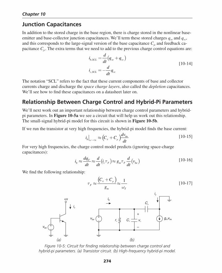
Chapter 10
274
Junction CapacitancesIn addition to the stored charge in the base region, there is charge stored in the nonlinear base-emitter and base-collector junction capacitances. We’ll term these stored charges qve and qvc, and this corresponds to the large-signal version of the base capacitance Cje and feedback ca-pacitance Cjc. The extra terms that we need to add to the previous charge control equations are:
( ),
,
b SCL ve vc
c SCL vc
di q q
dtd
i qdt
= +
= − [10-14]
The notation “SCL” refers to the fact that these current components of base and collector currents charge and discharge the space charge layers, also called the depletion capacitances. We’ll see how to fi nd these capacitances on a datasheet later on.
Relationship Between Charge Control and Hybrid-Pi ParametersWe’ll next work out an important relationship between charge control parameters and hybrid-pi parameters. In Figure 10-5a we see a circuit that will help us work out this relationship. The small-signal hybrid-pi model for this circuit is shown in Figure 10-5b.
If we run the transistor at very high frequencies, the hybrid-pi model fi nds the base current:
( ) beb
dvi C C
dtπ μω→∞≈ + [10-15]
For very high frequencies, the charge control model predicts (ignoring space-charge capacitances):
( ) ( )Fb c F m F be
dq d di i g v
dt dt dtτ τ≈ ≈ ≈ [10-16]
We fi nd the following relationship:
( ) 1
Fm T
C C
gπ μτ
ω
+≈ ≈ [10-17]
(a) (b)
Figure 10-5: Circuit for fi nding relationship between charge control and hybrid-pi parameters. (a) Transistor circuit. (b) High-frequency hybrid-pi model.
+v
ic
vbe
ib
ic
gmvberπ Cπ vπ
+
–
vbe
Cμ
Thompson Book.indb 274 3/20/2006 11:35:57 AM

Bipolar Transistor Switching and the Charge Control Model
275
Next, by looking at the charge control equations at very low frequencies, we fi nd:
Fb DC
BF
Fc
F
c BFBF F F
b FDC
qi
qi
i
i
τ
τ
ττ β τ
τ
=
=
= → =
[10-18]
So, we now have a relationship between the charge control parameters τF and τBF and the hybrid-pi parameters βF and ωT.
Finding Junction Capacitances from the DatasheetHow do we fi nd the values of junction capacitances? Well, we’re fortunate if manufacturers’ data is available. For instance, for the 2N3904 transistor, capacitance data is available for reverse bias voltages in excess of 0.1 volts (i.e., junction voltages less than –0.1V) on both the emitter-base and collector-base junctions, as shown in Figure 10-6.
5 From On Semiconductor, http://www.onsemi.com, reprinted with permission of On Semiconductor.
Figure 10-6: Manufacturer’s datasheet5 tabulation of junction capacitance of 2N3904 transistor.
What do we do if we need charge data for positive voltages on the base-emitter junction? An NPN transistor is cutoff for VBE less than 0.4V or so. The datasheet doesn’t give us capaci-tance values for positive VBE. Fortunately, there is a little bit of physics that’s available to us. The junction capacitance of a PN junction is given by:
1
joj m
j
BI
CC
V
V
=⎡ ⎤⎢ ⎥−⎢ ⎥⎣ ⎦
[10-19]
REVERSE BIAS VOLTAGE (VOLTS)
2.0
3.0
5.0
7.0
10
1.00.1
CA
PA
CIT
AN
CE
(pF
)
1.0 2.0 3.0 5.0 7.0 10 20 30 400.2 0.3 0.5 0.7
Cibo
Cobo
Thompson Book.indb 275 3/20/2006 11:35:58 AM
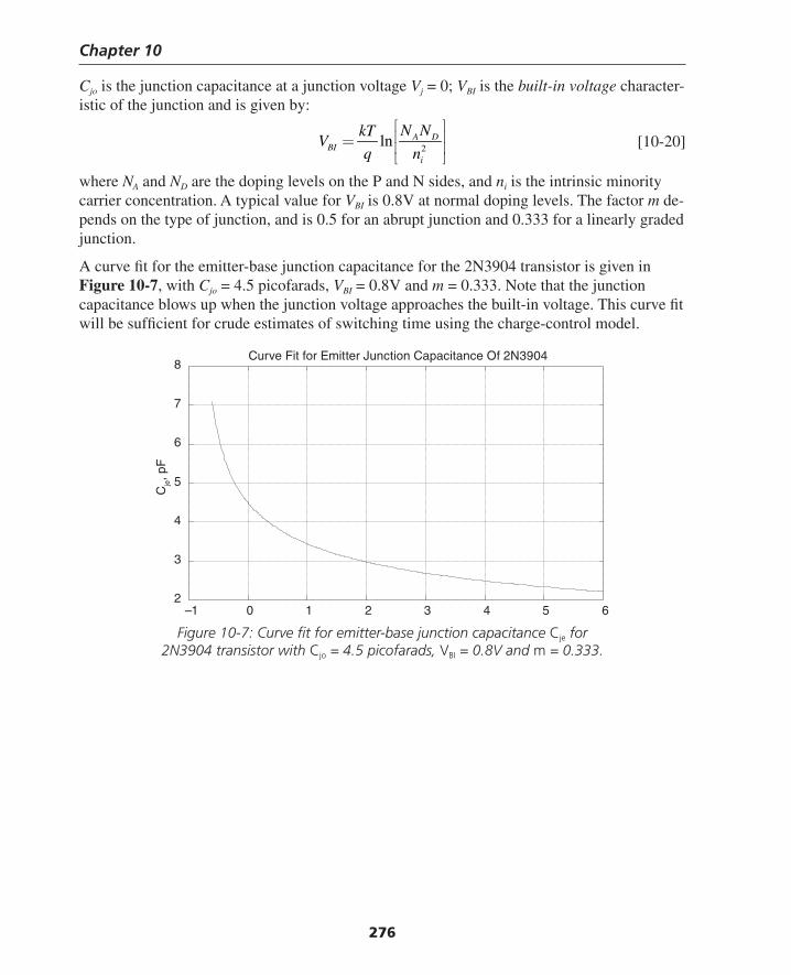
Chapter 10
276
Cjo is the junction capacitance at a junction voltage Vj = 0; VBI is the built-in voltage character-istic of the junction and is given by:
2ln A D
BIi
N NkTV
q n
⎡ ⎤⎢ ⎥= ⎢ ⎥⎣ ⎦
[10-20]
where NA and ND are the doping levels on the P and N sides, and ni is the intrinsic minority carrier concentration. A typical value for VBI is 0.8V at normal doping levels. The factor m de-pends on the type of junction, and is 0.5 for an abrupt junction and 0.333 for a linearly graded junction.
A curve fi t for the emitter-base junction capacitance for the 2N3904 transistor is given in Figure 10-7, with Cjo = 4.5 picofarads, VBI = 0.8V and m = 0.333. Note that the junction capacitance blows up when the junction voltage approaches the built-in voltage. This curve fi t will be suffi cient for crude estimates of switching time using the charge-control model.
Figure 10-7: Curve fi t for emitter-base junction capacitance Cje for 2N3904 transistor with Cjo = 4.5 picofarads, VBI = 0.8V and m = 0.333.
–1 0 1 2 3 4 5 62
3
4
5
6
7
8
Cje, p
F
Curve Fit for Emitter Junction Capacitance Of 2N3904
Thompson Book.indb 276 3/20/2006 11:35:58 AM
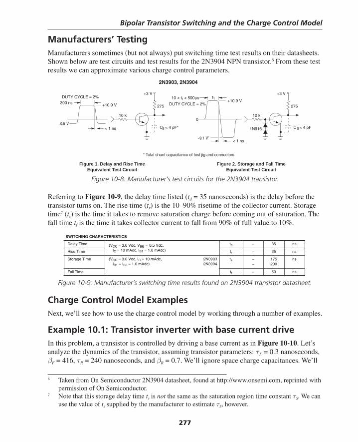
Bipolar Transistor Switching and the Charge Control Model
277
Manufacturers’ Testing Manufacturers sometimes (but not always) put switching time test results on their datasheets. Shown below are test circuits and test results for the 2N3904 NPN transistor.6 From these test results we can approximate various charge control parameters.
6 Taken from On Semiconductor 2N3904 datasheet, found at http://www.onsemi.com, reprinted with permission of On Semiconductor.
7 Note that this storage delay time ts is not the same as the saturation region time constant τS. We can use the value of ts supplied by the manufacturer to estimate τS, however.
Figure 10-8: Manufacturer’s test circuits for the 2N3904 transistor.
Referring to Figure 10-9, the delay time listed (td = 35 nanoseconds) is the delay before the transistor turns on. The rise time (tr) is the 10–90% risetime of the collector current. Storage time7 (ts) is the time it takes to remove saturation charge before coming out of saturation. The fall time tf is the time it takes collector current to fall from 90% of full value to 10%.
2N3903, 2N3904
Figure 1. Delay and Rise TimeEquivalent Test Circuit
Figure 2. Storage and Fall TimeEquivalent Test Circuit
+3 V
275
10 k
1N916 CS < 4 pF
+3 V
275
10 k
CS < 4 pF*< 1 ns
+10.9 V300 nsDUTY CYCLE = 2%
< 1 ns′
+10.9 VDUTY CYCLE = 2%
t1
0
10 < t1 < 500 s
* Total shunt capacitance of test jig and connectors
Figure 10-9: Manufacturer’s switching time results found on 2N3904 transistor datasheet.
Charge Control Model ExamplesNext, we’ll see how to use the charge control model by working through a number of examples.
Example 10.1: Transistor inverter with base current driveIn this problem, a transistor is controlled by driving a base current as in Figure 10-10. Let’s analyze the dynamics of the transistor, assuming transistor parameters: τF = 0.3 nanoseconds, βF = 416, τR = 240 nanoseconds, and βR = 0.7. We’ll ignore space charge capacitances. We’ll
SWITCHING CHARACTERISTICS
Delay Time (VCC = 3.0 Vdc, VBE = 0.5 Vdc, td − 35 ns
Rise Time
(VCC 3.0 Vdc, VBE 0.5 Vdc,IC = 10 mAdc, IB1 = 1.0 mAdc) tr − 35 ns
Storage Time (VCC = 3.0 Vdc, IC 3093N2,cdAm 01 = IB1 = IB2 4093N2)cdAm 0.1 =
ts −−
175200
ns
Fall Time tf − 50 ns
Thompson Book.indb 277 3/20/2006 11:35:59 AM
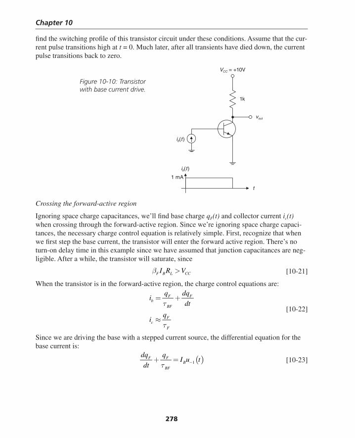
Chapter 10
278
fi nd the switching profi le of this transistor circuit under these conditions. Assume that the cur-rent pulse transitions high at t = 0. Much later, after all transients have died down, the current pulse transitions back to zero.
Crossing the forward-active region
Ignoring space charge capacitances, we’ll fi nd base charge qF(t) and collector current ic(t) when crossing through the forward-active region. Since we’re ignoring space charge capaci-tances, the necessary charge control equation is relatively simple. First, recognize that when we fi rst step the base current, the transistor will enter the forward active region. There’s no turn-on delay time in this example since we have assumed that junction capacitances are neg-ligible. After a while, the transistor will saturate, since
F B L CCI R Vβ > [10-21]
When the transistor is in the forward-active region, the charge control equations are:
F Fb
BF
Fc
F
q dqi
dt
qi
τ
τ
= +
≈ [10-22]
Since we are driving the base with a stepped current source, the differential equation for the base current is:
( )1F F
BBF
dq qI u t
dt τ −+ = [10-23]
VCC = +10V
1k
1 mA
t
vout
ib(t )
ib(t )
Figure 10-10: Transistor with base current drive.
Thompson Book.indb 278 3/20/2006 11:35:59 AM
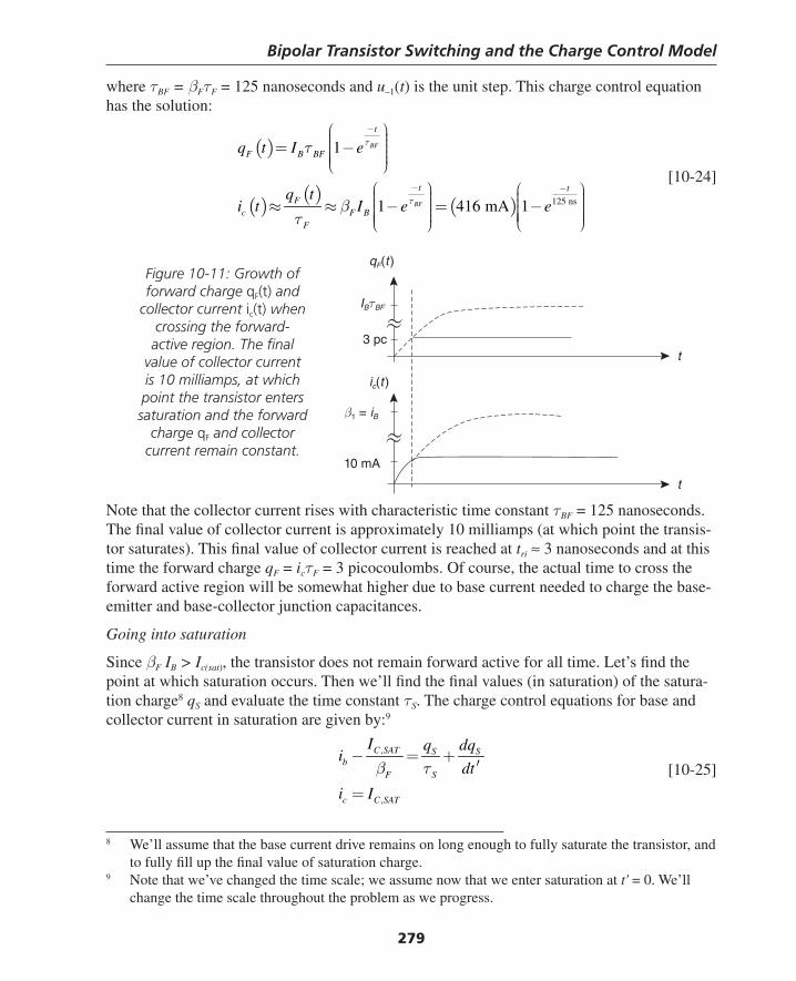
Bipolar Transistor Switching and the Charge Control Model
279
where τBF = βFτF = 125 nanoseconds and u–1(t) is the unit step. This charge control equation has the solution:
( )
( )( )
( ) 125 ns
1
1 416 mA 1
BF
BF
t
F B BF
t tF
c F BF
q t I e
q ti t I e e
τ
τ
τ
βτ
−
− −
⎛ ⎞⎟⎜ ⎟⎜= − ⎟⎜ ⎟⎜ ⎟⎜⎝ ⎠⎛ ⎞ ⎛ ⎞⎟ ⎟⎜ ⎜⎟ ⎟⎜ ⎜≈ ≈ − = −⎟ ⎟⎜ ⎜⎟ ⎟⎜ ⎜ ⎟⎟ ⎜⎜ ⎝ ⎠⎝ ⎠
[10-24]
8 We’ll assume that the base current drive remains on long enough to fully saturate the transistor, and to fully fi ll up the fi nal value of saturation charge.
9 Note that we’ve changed the time scale; we assume now that we enter saturation at t' = 0. We’ll change the time scale throughout the problem as we progress.
Note that the collector current rises with characteristic time constant τBF = 125 nanoseconds. The fi nal value of collector current is approximately 10 milliamps (at which point the transis-tor saturates). This fi nal value of collector current is reached at tri ≈ 3 nanoseconds and at this time the forward charge qF = icτF = 3 picocoulombs. Of course, the actual time to cross the forward active region will be somewhat higher due to base current needed to charge the base-emitter and base-collector junction capacitances.
Going into saturation
Since βF IB > Ic(sat), the transistor does not remain forward active for all time. Let’s fi nd the point at which saturation occurs. Then we’ll fi nd the fi nal values (in saturation) of the satura-tion charge8 qS and evaluate the time constant τS. The charge control equations for base and collector current in saturation are given by:9
,
,
C SAT S Sb
F S
c C SAT
I q dqi
dt
i I
β τ− = +
′
= [10-25]
t
qF(t )
IBτBF
≈3 pc
t
ic(t )
β1 = iB
≈10 mA
Figure 10-11: Growth of forward charge qF(t) and
collector current ic(t) when crossing the forward-active region. The fi nal
value of collector current is 10 milliamps, at which point the transistor enters saturation and the forward
charge qF and collector current remain constant.
Thompson Book.indb 279 3/20/2006 11:36:00 AM
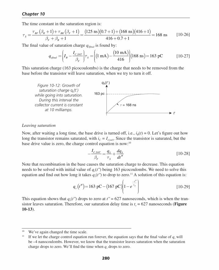
Chapter 10
280
The time constant in the saturation region is:
( ) ( ) ( )( ) ( )( )1 1 125 ns 0.7 1 168 ns 416 1168 ns
1 416 0.7 1BF R BR F
SF R
τ β τ βτ
β β
+ + + + + += = =
+ + + + [10-26]
The fi nal value of saturation charge qSfi nal is found by:
( )( )
( ), 10 mA1 mA 168 ns 163 pC
416C SAT
sfinal B SF
Iq I τ
β
⎛ ⎞⎛ ⎞ ⎟⎟ ⎜⎜ ⎟⎟ ⎜= − = − =⎜ ⎟⎟ ⎜⎜ ⎟⎟⎜ ⎟⎜⎝ ⎠ ⎝ ⎠ [10-27]
This saturation charge (163 picocoulombs) is the charge that needs to be removed from the base before the transistor will leave saturation, when we try to turn it off.
Leaving saturation
Now, after waiting a long time, the base drive is turned off, i.e., iB(t) = 0. Let’s fi gure out how long the transistor remains saturated, with iC = Ic(sat). Since the transistor is saturated, but the base drive value is zero, the charge control equation is now:10
,C SAT S S
F S
I q dq
dtβ τ− = +
′′ [10-28]
Note that recombination in the base causes the saturation charge to decrease. This equation needs to be solved with initial value of qs(t'') being 163 picocoulombs. We need to solve this equation and fi nd out how long it takes qs(t'') to drop to zero.11 A solution of this equation is:
( ) ( )163 pC 167 pC 1 S
t
sq t e τ′′−⎛ ⎞⎟⎜ ⎟⎜′′ = − − ⎟⎜ ⎟⎜ ⎟⎜⎝ ⎠
[10-29]
This equation shows that qs(t'') drops to zero at t'' = 627 nanoseconds, which is when the tran-sistor leaves saturation. Therefore, our saturation delay time is ts = 627 nanoseconds (Figure 10-13).
t'
qS(t' )
163 pc
τ = 168 ns
Figure 10-12: Growth of saturation charge qs(t')
while going into saturation. During this interval the
collector current is constant at 10 milliamps.
10 We’ve again changed the time scale.11 If we let the charge control equation run forever, the equation says that the fi nal value of qs will
be –4 nanocoulombs. However, we know that the transistor leaves saturation when the saturation charge drops to zero. We’ll fi nd the time when qs drops to zero.
Thompson Book.indb 280 3/20/2006 11:36:00 AM
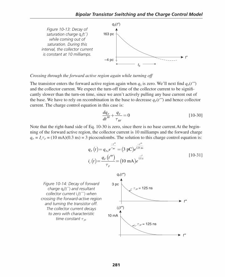
Bipolar Transistor Switching and the Charge Control Model
281
Crossing through the forward active region again while turning off
The transistor enters the forward active region again when qS is zero. We’ll next fi nd qF(t''') and the collector current. We expect the turn-off time of the collector current to be signifi -cantly slower than the turn-on time, since we aren’t actively pulling any base current out of the base. We have to rely on recombination in the base to decrease qF(t''') and hence collector current. The charge control equation in this case is:
0F F
BF
dq q
dt τ+ =
′′′ [10-30]
Note that the right-hand side of Eq. 10-30 is zero, since there is no base current.At the begin-ning of the forward active region, the collector current is 10 milliamps and the forward charge qF = IcτF = (10 mA)(0.3 ns) = 3 picocoulombs. The solution to this charge control equation is:
( ) ( )
( )( )
( )125 ns
125 ns3 pC
10 mA
BF
t
t t
F Fo
Fc
F
q t q e e
q ti t e
τ
τ
′′′−
′′′ ′′′− −
= =
′′′= =
[10-31]
t"
qS(t" )
163 pc
tS
–4 pc
Figure 10-13: Decay of saturation charge qs(t´´)
while coming out of saturation. During this
interval, the collector current is constant at 10 milliamps.
Figure 10-14: Decay of forward charge qF(t´´ ) and resultant
collector current ic(t´´´ ) when crossing the forward-active region
and turning the transistor off.The collector current decays to zero with characteristic
time constant τβF.
t"'
qF(t"' )
3 pcτβF = 125 ns
t"'
ic(t"' )
10 mA
τβF = 125 ns
Thompson Book.indb 281 3/20/2006 11:36:01 AM
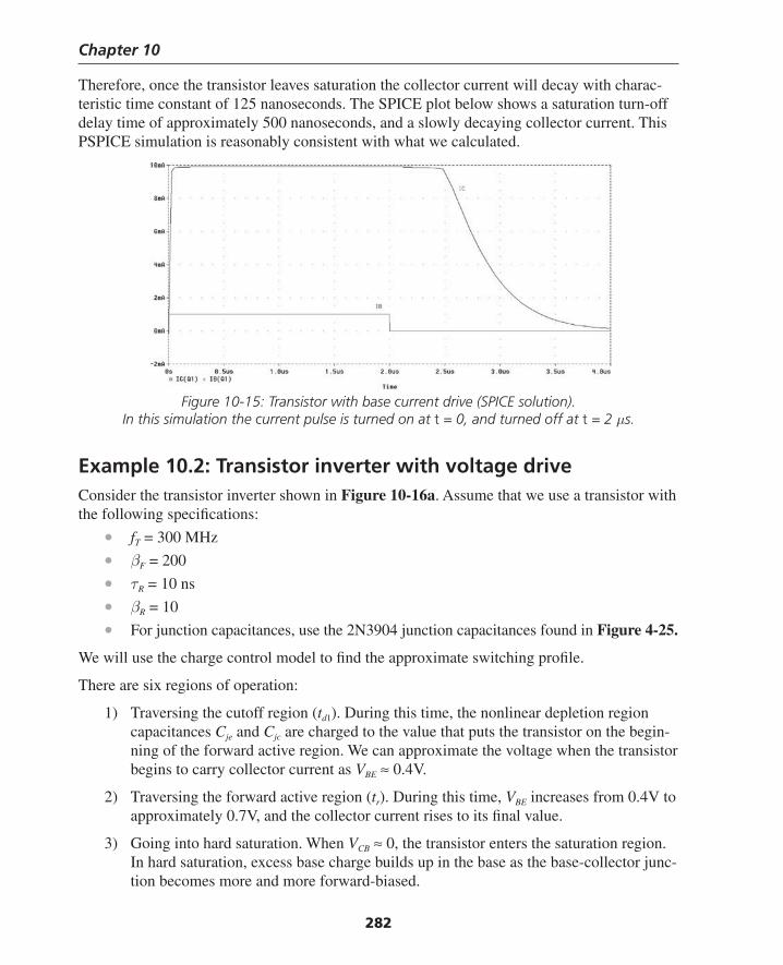
Chapter 10
282
Therefore, once the transistor leaves saturation the collector current will decay with charac-teristic time constant of 125 nanoseconds. The SPICE plot below shows a saturation turn-off delay time of approximately 500 nanoseconds, and a slowly decaying collector current. This PSPICE simulation is reasonably consistent with what we calculated.
Figure 10-15: Transistor with base current drive (SPICE solution). In this simulation the current pulse is turned on at t = 0, and turned off at t = 2 μs.
Example 10.2: Transistor inverter with voltage driveConsider the transistor inverter shown in Figure 10-16a. Assume that we use a transistor with the following specifi cations:
• fT = 300 MHz
• βF = 200
• τR = 10 ns
• βR = 10
• For junction capacitances, use the 2N3904 junction capacitances found in Figure 4-25.
We will use the charge control model to fi nd the approximate switching profi le.
There are six regions of operation:
1) Traversing the cutoff region (td1). During this time, the nonlinear depletion region capacitances Cje and Cjc are charged to the value that puts the transistor on the begin-ning of the forward active region. We can approximate the voltage when the transistor begins to carry collector current as VBE ≈ 0.4V.
2) Traversing the forward active region (tr). During this time, VBE increases from 0.4V to approximately 0.7V, and the collector current rises to its fi nal value.
3) Going into hard saturation. When VCB ≈ 0, the transistor enters the saturation region. In hard saturation, excess base charge builds up in the base as the base-collector junc-tion becomes more and more forward-biased.
Thompson Book.indb 282 3/20/2006 11:36:02 AM
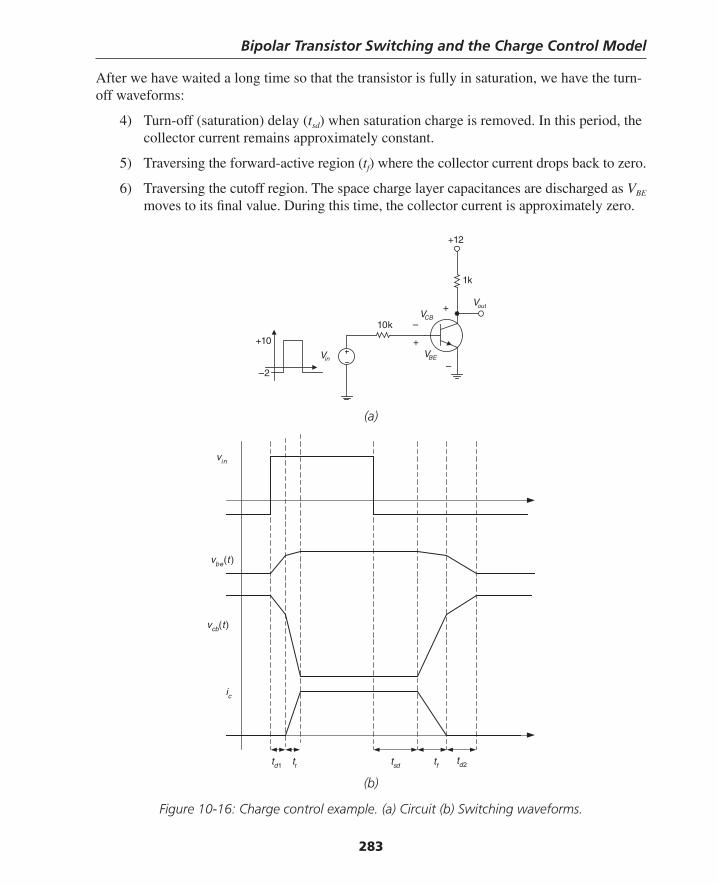
Bipolar Transistor Switching and the Charge Control Model
283
After we have waited a long time so that the transistor is fully in saturation, we have the turn-off waveforms:
4) Turn-off (saturation) delay (tsd) when saturation charge is removed. In this period, the collector current remains approximately constant.
5) Traversing the forward-active region (tf) where the collector current drops back to zero.
6) Traversing the cutoff region. The space charge layer capacitances are discharged as VBE moves to its fi nal value. During this time, the collector current is approximately zero.
(a)
(b)
Figure 10-16: Charge control example. (a) Circuit (b) Switching waveforms.
10k
1k
Vout
+12
Vin
–2
+10
–
+VCB
+
–VBE
vin
ic
td1 tr tsd tf td2
vbe(t )
vcb(t)
Thompson Book.indb 283 3/20/2006 11:36:02 AM
Chapter 10
284
Calculations for the various regions are as follows:
Cutoff region: At t = 0, we assume that the input instantaneously transitions from –2V to +10V. The turn-on delay time td1 is the time that it takes to charge the nonlinear collector-base and base-emitter capacitances so that VBE = 0.4V, which we will take as the beginning of the forward-active region. During this charging interval, the base current does vary a little bit, since the VBE changes, but for simplicity we’ll use the average base current to determine the switching time. Terminal conditions are:
At the beginning of the switching interval, at t = 0:
VBE = –2V
VCB = +14
Cje = 2.9 picofarads @ VBE = –2V
qve= CjeVBE = (2.9 picofarads)(–2V) = –5.8 picocoulombs
Cjc = 1.5 picofarads @ VCB = +14V
qvc = CjcVCE = (1.5 picofarads)(14V) = 21 picocoulombs
ib(t = 0) = (10V – –2V)/10k = 1.2 mA
ic(t = 0) = 0
At the very beginning of the forward active region, t = td1:
VBE = 0.4V
VCB = +11.6
Cje ≈ 8 picofarads @ VBE = 0.4 V; (this is an estimate, since the curves on the datasheet don’t extend to positive voltages).
qve= CjeVBE = (8 picofarads)(0.4V) = +3.2 picocoulombs
Cjc = 1.6 picofarads @ VCB = +11.6V
qvc = CjcVCE = (1.6 picofarads)(11.6V) = 18.6 picocoulombs
ib(t = td1) = (10V – 0.4V)/10k = 0.96 mA
ic(t = td1) = 0
The average base current ib,avg = 1.08 milliamps during this charging interval in the cutoff region. The change in charge in the nonlinear base-emitter capacitance is Δqve = (5.8 picocoulombs + 3.2 picocoulombs), resulting in Δqve = 9 picocoulombs. A similar calculation for the collector-base junction results in Δqvc = 2.4 picocoulombs. The time to charge is approximated by:
1,
10.4 pC10 ns
1.08 mAve vc
db avg
q qt
i
Δ + Δ≈ = ≈ [10-32]
During this interval, the collector current is zero.
Traversing the forward active region: At t = td1, we assume that the transistor begins to turn on and the collector current begins to rise, until saturation is reached. The rise time tr depends on the rate that we can both charge the nonlinear junction capacitances, as well as supply the
Thompson Book.indb 284 3/20/2006 11:36:03 AM
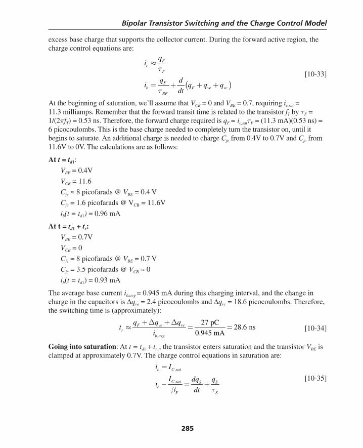
Bipolar Transistor Switching and the Charge Control Model
285
excess base charge that supports the collector current. During the forward active region, the charge control equations are:
( )
Fc
F
Fb F ve vc
BF
qi
q di q q q
dt
τ
τ
≈
= + + + [10-33]
At the beginning of saturation, we’ll assume that VCB = 0 and VBE = 0.7, requiring ic,sat = 11.3 milliamps. Remember that the forward transit time is related to the transistor fT by τF = 1/(2πfT) = 0.53 ns. Therefore, the forward charge required is qF
= ic,satτF = (11.3 mA)(0.53 ns) = 6 picocoulombs. This is the base charge needed to completely turn the transistor on, until it begins to saturate. An additional charge is needed to charge Cje from 0.4V to 0.7V and Cjc from 11.6V to 0V. The calculations are as follows:
At t = td1:
VBE = 0.4V
VCB = 11.6
Cje ≈ 8 picofarads @ VBE = 0.4 V
Cjc = 1.6 picofarads @ VCB = 11.6V
ib(t = td1) = 0.96 mA
At t = td1 + tr:
VBE = 0.7V
VCB = 0
Cje ≈ 8 picofarads @ VBE = 0.7 V
Cjc = 3.5 picofarads @ VCB ≈ 0
ib(t = td1) = 0.93 mA
The average base current ib,avg = 0.945 mA during this charging interval, and the change in charge in the capacitors is Δqve = 2.4 picocoulombs and Δqvc = 18.6 picocoulombs. Therefore, the switching time is (approximately):
,
27 pC28.6 ns
0.945 mAF ve vc
rb avg
q q qt
i
+ Δ + Δ≈ = = [10-34]
Going into saturation: At t = td1 + tr1, the transistor enters saturation and the transistor VBE is clamped at approximately 0.7V. The charge control equations in saturation are:
,
,
c C sat
C sat S Sb
F S
i I
I dq qi
dtβ τ
=
− = + [10-35]
Thompson Book.indb 285 3/20/2006 11:36:03 AM
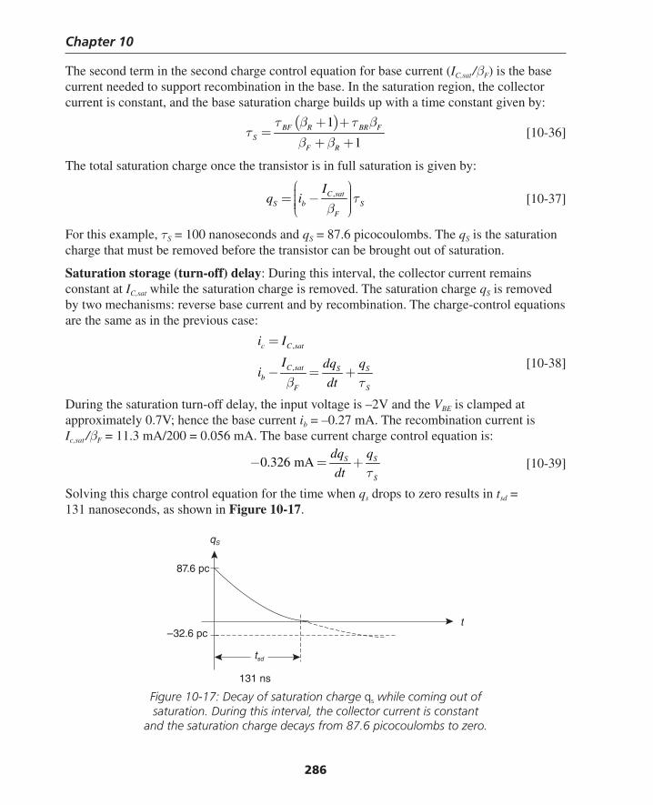
Chapter 10
286
The second term in the second charge control equation for base current (IC,sat /βF) is the base current needed to support recombination in the base. In the saturation region, the collector current is constant, and the base saturation charge builds up with a time constant given by:
( )1
1BF R BR F
SF R
τ β τ βτ
β β
+ +=
+ + [10-36]
The total saturation charge once the transistor is in full saturation is given by:
,C satS b S
F
Iq i τ
β
⎛ ⎞⎟⎜ ⎟= −⎜ ⎟⎜ ⎟⎜⎝ ⎠ [10-37]
For this example, τS = 100 nanoseconds and qS = 87.6 picocoulombs. The qS is the saturation charge that must be removed before the transistor can be brought out of saturation.
Saturation storage (turn-off) delay: During this interval, the collector current remains constant at IC,sat while the saturation charge is removed. The saturation charge qS is removed by two mechanisms: reverse base current and by recombination. The charge-control equations are the same as in the previous case:
,
,
c C sat
C sat S Sb
F S
i I
I dq qi
dtβ τ
=
− = + [10-38]
During the saturation turn-off delay, the input voltage is –2V and the VBE is clamped at approximately 0.7V; hence the base current ib = –0.27 mA. The recombination current is Ic,sat /βF = 11.3 mA/200 = 0.056 mA. The base current charge control equation is:
0.326 mA S S
S
dq q
dt τ− = + [10-39]
Solving this charge control equation for the time when qs drops to zero results in tsd = 131 nanoseconds, as shown in Figure 10-17.
Figure 10-17: Decay of saturation charge qs while coming out of saturation. During this interval, the collector current is constant
and the saturation charge decays from 87.6 picocoulombs to zero.
t
qS
–32.6 pc
131 ns
tsd
87.6 pc
Thompson Book.indb 286 3/20/2006 11:36:03 AM
Bipolar Transistor Switching and the Charge Control Model
287
Forward-active region (current falltime): After leaving saturation, we again enter the for-ward-active region. In order to turn the transistor off and traverse the forward-active region, we need to remove the base charge qF as well as discharge the nonlinear depletion capacitanc-es. At the beginning of the current falltime interval:
VBE = 0.7V
VCB ≈ 0
Cje ≈ 8 picofarads @ VBE = 0.7V
Cjc = 3.5 picofarads @ VCB = 0
ib = 0.27 mA
At the end of the falltime interval:
VBE = 0.4V
VCB = 11.6
Cje ≈ 8 picofarads @ VBE = 0.4V
Cjc = 1.6 picofarads @ VCB = 11.6V
ib = 0.24 mA
The base charge qF that we need to remove is the same as in the turn-on case (qF = 6 picocou-lombs). The change in charge in the depletion regions is also the same as in the turn-on case, resulting in:
,
27 pC106 ns
0.255 mAF ve vc
fb avg
q q qt
i
+ Δ + Δ≈ = = [10-40]
Note that even though the total charge supplied is the same as in the turn-on case, the turn-off time is much longer since the average base current is lower.
Cutoff: During this interval, we discharge the nonlinear capacitances back to their fi nal values. The total gate charge required is the same as the turn-on case, where the charge is 11.44 picocoulombs. In this case the average base current over the interval is approximately 0.12 mA, resulting in a total turnoff delay time of:
2,
11.44 pC95.3 ns
0.12 mAve vc
db avg
q qt
i
Δ + Δ≈ = = [10-41]
A SPICE simulation for the inverter is shown in Figure 10-18. Table 10-1 shows a compari-son of the charge control calculations with the SPICE calculations. This result shows that the charge control model is a useful approximation technique for calculating the switching times. More importantly, the model shows how to speed up the switching process. In this example, the output risetime and falltime can be signifi cantly reduced by reducing the base resistor.
Thompson Book.indb 287 3/20/2006 11:36:04 AM
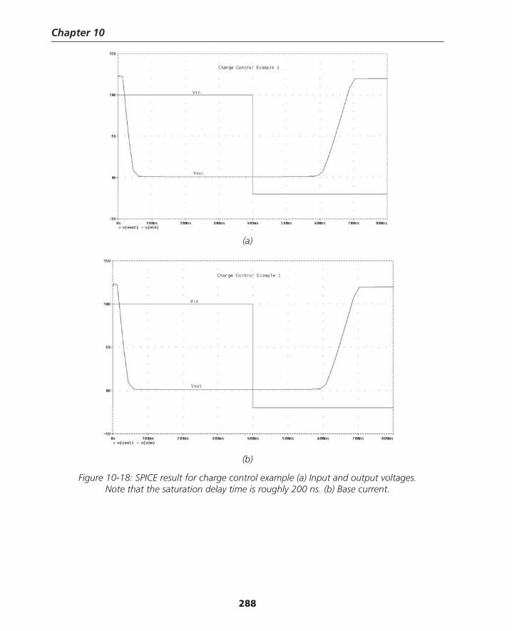
Chapter 10
288
(a)
(b)
Figure 10-18: SPICE result for charge control example (a) Input and output voltages. Note that the saturation delay time is roughly 200 ns. (b) Base current.
Thompson Book.indb 288 3/20/2006 11:36:04 AM
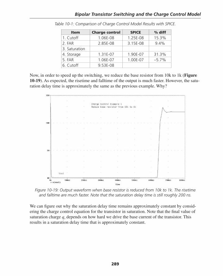
Bipolar Transistor Switching and the Charge Control Model
289
Table 10-1: Comparison of Charge Control Model Results with SPICE.
Item Charge control SPICE % diff1. Cutoff 1.06E-08 1.25E-08 15.3%2. FAR 2.85E-08 3.15E-08 9.4%3. Saturation 4. Storage 1.31E-07 1.90E-07 31.3%5. FAR 1.06E-07 1.00E-07 –5.7%6. Cutoff 9.53E-08
Now, in order to speed up the switching, we reduce the base resistor from 10k to 1k (Figure 10-19). As expected, the risetime and falltime of the output is much faster. However, the satu-ration delay time is approximately the same as the previous example. Why?
Figure 10-19: Output waveform when base resistor is reduced from 10k to 1k. The risetime and falltime are much faster. Note that the saturation delay time is still roughly 200 ns.
We can fi gure out why the saturation delay time remains approximately constant by consid-ering the charge control equation for the transistor in saturation. Note that the fi nal value of saturation charge qs depends on how hard we drive the base current of the transistor. This results in a saturation delay time that is approximately constant.
Thompson Book.indb 289 3/20/2006 11:36:05 AM
Chapter 10
290
Example 10.3: Nonsaturating current switchA nonsaturating current switch implemented with 2N2222 signal transistors is shown in Fig-ure 10-20. If we ignore junction capacitances, the relevant charge control equations for the base and collector currents are:
F Fb
BF
Fc
F
q dqi
dt
qi
τ
τ
= +
= [10-42]
In order to turn the transistors ON and OFF fast, we need to supply base current to charge and discharge qF for each transistor. Therefore, in large part, the switching speed is determined by how much base current we can supply. The base current in this voltage-driven case is set by the voltage swing of the base drivers and the base spreading resistance rx of the transistors. For the 2N2222 transistor,12 the value of the base spreading resistance is very roughly rx ≈ 40Ω.
We’ll assume a 2V swing for the base drivers vb1(t) and vb2(t), so the maximum base current is ∼50 mA. We can solve for the switching time as:
, , ,F final C final F C finalSW
b b T b
q I I
i i i
ττ
ω≈ ≈ ≈ [10-43]
where the notation <ib> denotes the average value of base current during switching. The ac-tual switching time will be longer, due to the fact that the same base current must charge the nonlinear base-collector and base-emitter junction capacitances. The important result from this is that the switching time will approximately scale with the collector current, if the base current remains constant. Figure 10-21 is a transient SPICE simulation for IBIAS levels of 100 mA, 200 mA and 300 mA. We note that the switching time is a few nanoseconds13 in each
12 This is a crude approximation since the value of the base spreading resistance varies with collector current bias level.
13 Note that a nanosecond is a very short period of time. Light travels about a foot in a nanosecond.
vb1 vb2
–12
Ibias
Q1 Q2
2N2222 2N2222
Figure 10-20: Differential current switch.
Thompson Book.indb 290 3/20/2006 11:36:06 AM
Bipolar Transistor Switching and the Charge Control Model
291
case and this switching time does increase approximately proportionally with the bias current level, as expected. Figure 10-22 is a transient SPICE plot of base current. During the transi-tion of the collector current, the base currents are high.
Figure 10-21: Current switch simulation, showing collector current of Q1.
Figure 10-22: Current switch simulation, showing base current of Q1.
Thompson Book.indb 291 3/20/2006 11:36:06 AM
Chapter 10
292
Emitter SwitchingAn emitter switch is shown in Figure 10-23. This type of topology has been used in power switches where high voltage isolation to the load is needed. As shown in Figure 10-23b, the MOSFET provides the high speed current switching, and the bipolar transistor is a common-base buffer which provides voltage isolation. Note that in the emitter switching case, there is no problem with transistor saturation. Hence, we expect this type of switch to be fast. We’ll estimate the switching speed of this type of topology assuming that the MOSFET provides a step of current to the emitter of the transistor.
(a) (b)
Figure 10-23: Emitter switching. (a) Circuit. (b) Implementation as a high voltage switch with the low-side MOSFET providing the fast
switching current, and the transistor providing the high-voltage buffering.
Referring to Figure 10-23a and ignoring junction capacitances, the relevant charge control equations are:
( )
F Fb
BF
Fc
F
F F Fe b c
BF F
q dqi
dt
qi
q dq qi i i
dt
τ
τ
τ τ
= +
=
= − + = − − −
[10-44]
Rearranging the above emitter charge control equation results in:
( )1F F F
EBF F
q dq qI u t
dtτ τ −− − − = − [10-45]
where u–1(t) is the unit step. We can make a further approximation for the emitter charge con-trol equation by noting that τBF >> τF and hence qF /τBF << qF /τF, resulting in:
vBIAS
+vCC
ic
ie(t )
–vEE
+vCC
vC
vBIAS
ic
Thompson Book.indb 292 3/20/2006 11:36:07 AM
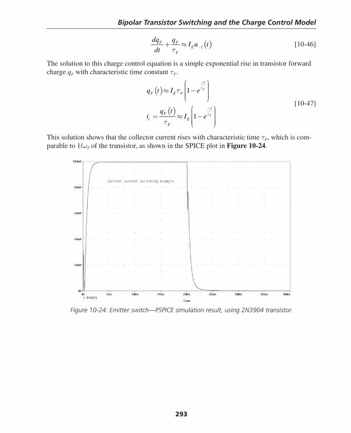
Bipolar Transistor Switching and the Charge Control Model
293
( )1F F
EF
dq qI u t
dt τ −+ ≈ [10-46]
The solution to this charge control equation is a simple exponential rise in transistor forward charge qF with characteristic time constant τF.
( )
( )
1
1
F
F
t
F E F
tF
c EF
q t I e
q ti I e
τ
τ
τ
τ
−
−
⎛ ⎞⎟⎜ ⎟⎜≈ − ⎟⎜ ⎟⎜ ⎟⎜⎝ ⎠⎛ ⎞⎟⎜ ⎟⎜= ≈ − ⎟⎜ ⎟⎜ ⎟⎜⎝ ⎠
[10-47]
This solution shows that the collector current rises with characteristic time τF, which is com-parable to 1/ωT of the transistor, as shown in the SPICE plot in Figure 10-24.
Figure 10-24: Emitter switch—PSPICE simulation result, using 2N3904 transistor.
Thompson Book.indb 293 3/20/2006 11:36:07 AM
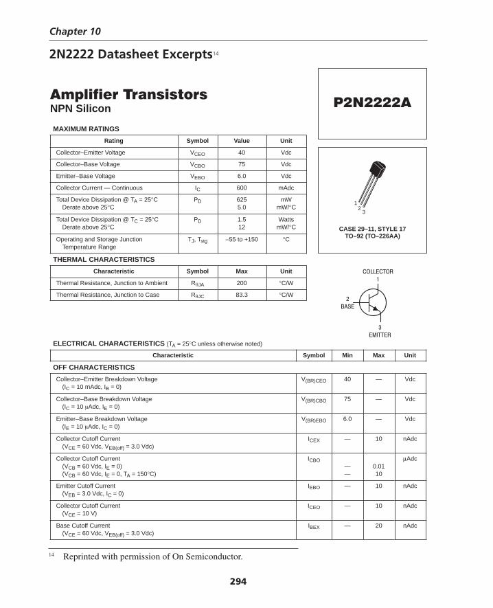
Chapter 10
294
2N2222 Datasheet Excerpts14
NPN Silicon
MAXIMUM RATINGSRating Symbol Value Unit
Collector–Emitter Voltage VCEO 40 Vdc
Collector–Base Voltage VCBO 75 Vdc
Emitter–Base Voltage VEBO 6.0 Vdc
Collector Current — Continuous IC 600 mAdc
Total Device Dissipation @ TA = 25°CDerate above 25°C
PD 6255.0
mWmW/°C
Total Device Dissipation @ TC = 25°CDerate above 25°C
PD 1.512
WattsmW/°C
Operating and Storage JunctionTemperature Range
TJ, Tstg –55 to +150 °C
THERMAL CHARACTERISTICSCharacteristic Symbol Max Unit
Thermal Resistance, Junction to Ambient R JA 200 °C/W
Thermal Resistance, Junction to Case R JC 83.3 °C/W
ELECTRICAL CHARACTERISTICS (TA = 25°C unless otherwise noted)
Characteristic Symbol Min Max Unit
OFF CHARACTERISTICSCollector–Emitter Breakdown Voltage
(IC = 10 mAdc, IB = 0)V(BR)CEO 40 — Vdc
Collector–Base Breakdown Voltage(IC = 10 Adc, IE = 0)
V(BR)CBO 75 — Vdc
Emitter–Base Breakdown Voltage(IE = 10 Adc, IC = 0)
V(BR)EBO 6.0 — Vdc
Collector Cutoff Current(VCE = 60 Vdc, VEB(off) = 3.0 Vdc)
ICEX — 10 nAdc
Collector Cutoff Current(VCB = 60 Vdc, IE = 0)(VCB = 60 Vdc, IE = 0, TA = 150°C)
ICBO——
0.0110
μAdc
Emitter Cutoff Current(VEB = 3.0 Vdc, IC = 0)
IEBO — 10 nAdc
Collector Cutoff Current(VCE = 10 V)
ICEO — 10 nAdc
Base Cutoff Current(VCE = 60 Vdc, VEB(off) = 3.0 Vdc)
IBEX — 20 nAdc
CASE 29–11, STYLE 17TO–92 (TO–226AA)
12
3
14 Reprinted with permission of On Semiconductor.
Thompson Book.indb 294 3/20/2006 11:36:08 AM
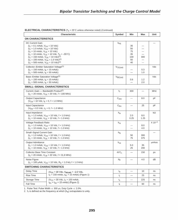
Bipolar Transistor Switching and the Charge Control Model
295
ELECTRICAL CHARACTERISTICS (TA = 25°C unless otherwise noted) (Continued)
Characteristic Symbol Min Max Unit
ON CHARACTERISTICSDC Current Gain
(IC = 0.1 mAdc, VCE = 10 Vdc)(IC = 1.0 mAdc, VCE = 10 Vdc)(IC = 10 mAdc, VCE = 10 Vdc)(IC = 10 mAdc, VCE = 10 Vdc, TA = –55°C)(IC = 150 mAdc, VCE = 10 Vdc)(1)
(IC = 150 mAdc, VCE = 1.0 Vdc)(1)
(IC = 500 mAdc, VCE = 10 Vdc)(1)
hFE355075351005040
————
300——
—
Collector–Emitter Saturation Voltage(1)
(IC = 150 mAdc, IB = 15 mAdc)(IC = 500 mAdc, IB = 50 mAdc)
VCE(sat)——
0.31.0
Vdc
Base–Emitter Saturation Voltage(1)
(IC = 150 mAdc, IB = 15 mAdc)(IC = 500 mAdc, IB = 50 mAdc)
VBE(sat)0.6—
1.22.0
Vdc
SMALL–SIGNAL CHARACTERISTICSCurrent–Gain — Bandwidth Product(2)
(IC = 20 mAdc, VCE = 20 Vdc, f = 100 MHz)fT 300 — MHz
Output Capacitance(VCB = 10 Vdc, IE = 0, f = 1.0 MHz)
Cobo — 8.0 pF
Input Capacitance(VEB = 0.5 Vdc, IC = 0, f = 1.0 MHz)
Cibo — 25 pF
Input Impedance(IC = 1.0 mAdc, VCE = 10 Vdc, f = 1.0 kHz)(IC = 10 mAdc, VCE = 10 Vdc, f = 1.0 kHz)
hie2.00.25
8.01.25
kΩ
Voltage Feedback Ratio(IC = 1.0 mAdc, VCE = 10 Vdc, f = 1.0 kHz)(IC = 10 mAdc, VCE = 10 Vdc, f = 1.0 kHz)
hre——
8.04.0
X 10–4
Small–Signal Current Gain(IC = 1.0 mAdc, VCE = 10 Vdc, f = 1.0 kHz)(IC = 10 mAdc, VCE = 10 Vdc, f = 1.0 kHz)
hfe5075
300375
—
Output Admittance(IC = 1.0 mAdc, VCE = 10 Vdc, f = 1.0 kHz)(IC = 10 mAdc, VCE = 10 Vdc, f = 1.0 kHz)
hoe5.025
35200
mhos
Collector Base Time Constant(IE = 20 mAdc, VCB = 20 Vdc, f = 31.8 MHz)
rb′Cc — 150 ps
Noise Figure(IC = 100 Adc, VCE = 10 Vdc, RS = 1.0 kΩ, f = 1.0 kHz)
NF — 4.0 dB
SWITCHING CHARACTERISTICSDelay Time (VCC = 30 Vdc, VBE(off) = –2.0 Vdc, td — 10 ns
Rise Time(VCC 30 Vdc, VBE(off) 2.0 Vdc,IC = 150 mAdc, IB1 = 15 mAdc) (Figure 1) tr — 25 ns
Storage Time (VCC = 30 Vdc, IC = 150 mAdc,I I 15 Ad ) (Fi 2)
ts — 225 ns
Fall TimeIB1 = IB2 = 15 mAdc) (Figure 2)
tf — 60 ns
1. Pulse Test: Pulse Width 300 s, Duty Cycle 2.0%.2. fT is defined as the frequency at which |hfe| extrapolates to unity.
Thompson Book.indb 295 3/20/2006 11:36:08 AM
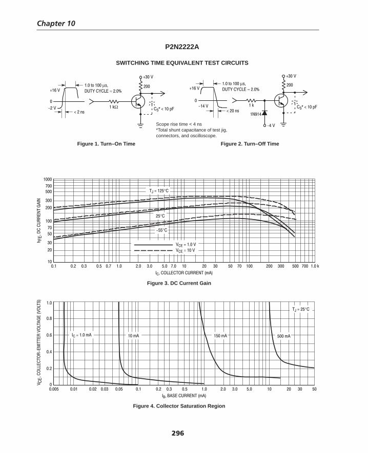
Chapter 10
296
P2N2222A
emiT ffO–nruT .2 erugiFemiT nO–nruT .1 erugiF
SWITCHING TIME EQUIVALENT TEST CIRCUITS
Scope rise time < 4 ns*Total shunt capacitance of test jig,connectors, and oscilloscope.
μ≈
Ω
μ≈
Figure 3. DC Current Gain
Figure 4. Collector Saturation Region
°
°
°
°
Thompson Book.indb 296 3/20/2006 11:36:09 AM
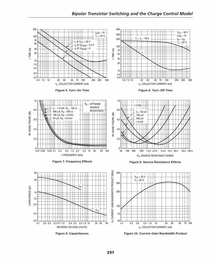
Bipolar Transistor Switching and the Charge Control Model
297
Figure 5. Turn–On Time
°
Figure 6. Turn–Off Time
°′
Figure 7. Frequency Effects Figure 8. Source Resistance Effects
Ωμ Ωμ Ω
μ Ω
μμμ
Figure 9. Capacitances Figure 10. Current–Gain Bandwidth Product
°
Thompson Book.indb 297 3/20/2006 11:36:09 AM
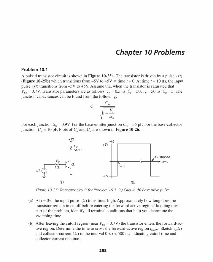
298
Chapter 10 Problems
Problem 10.1A pulsed transistor circuit is shown in Figure 10-25a. The transistor is driven by a pulse vi(t) (Figure 10-25b) which transitions from –5V to +5V at time t = 0. At time t = 10 μs, the input pulse vi(t) transitions from –5V to +5V. Assume that when the transistor is saturated that VBE = 0.7V. Transistor parameters are as follows: τF = 0.5 ns; βF = 50; τR = 50 ns; βR = 5. The junction capacitances can be found from the following:
1
joj
j
bi
CC
V
φ
=
−
For each junction φbi = 0.9V. For the base-emitter junction Cjo = 35 pF. For the base-collector junction, Cjo = 10 pF. Plots of Cje and Cjc are shown in Figure 10-26.
(a) (b)
Figure 10-25: Transistor circuit for Problem 10.1. (a) Circuit. (b) Base drive pulse.
(a) At t = 0+, the input pulse vi(t) transitions high. Approximately how long does the transistor remain in cutoff before entering the forward active region? In doing this part of the problem, identify all terminal conditions that help you determine the switching time.
(b) After leaving the cutoff region (near VBE = 0.7V) the transistor enters the forward-ac-tive region. Determine the time to cross the forward-active region tfar,ON. Sketch vbe(t) and collector current ic(t) in the interval 0 < t < 500 ns, indicating cutoff time and collector current risetime
≈
+12
vi(t)
RB
Q1
RC
510Ω
10k t = 0
vi(t)+5V
–5V
t = 10µsec
time
Thompson Book.indb 298 3/20/2006 11:36:09 AM
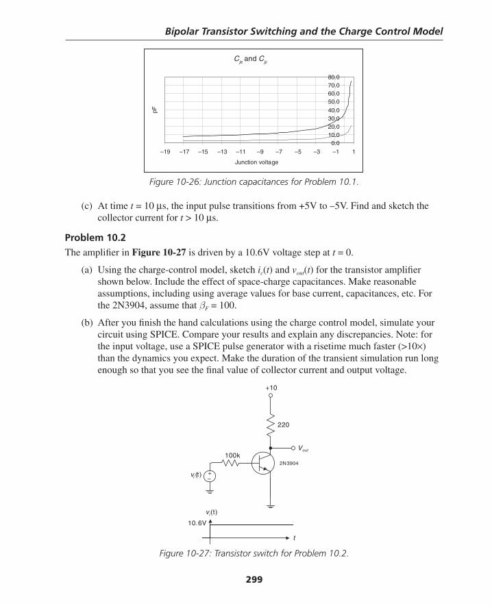
Bipolar Transistor Switching and the Charge Control Model
299
(c) At time t = 10 μs, the input pulse transitions from +5V to –5V. Find and sketch the collector current for t > 10 μs.
Problem 10.2The amplifi er in Figure 10-27 is driven by a 10.6V voltage step at t = 0.
(a) Using the charge-control model, sketch ic(t) and vout(t) for the transistor amplifi er shown below. Include the effect of space-charge capacitances. Make reasonable assumptions, including using average values for base current, capacitances, etc. For the 2N3904, assume that βF = 100.
(b) After you fi nish the hand calculations using the charge control model, simulate your circuit using SPICE. Compare your results and explain any discrepancies. Note: for the input voltage, use a SPICE pulse generator with a risetime much faster (>10×) than the dynamics you expect. Make the duration of the transient simulation run long enough so that you see the fi nal value of collector current and output voltage.
Cje and Cjc
0.010.020.030.040.0
50.060.070.080.0
–19 –17 –15 –13 –11 –9 –7 –5 –3 –1 1
Junction voltagepF
Figure 10-26: Junction capacitances for Problem 10.1.
Figure 10-27: Transistor switch for Problem 10.2.
Vout
+10
220
vi (t)
vi(t)
10.6V
t
+–
100k2N3904
Thompson Book.indb 299 3/20/2006 11:36:10 AM
Chapter 10
300
Problem 10.3In this problem, a 2N3904 transistor is controlled by a voltage drive as shown in Figure 10-28. Analyze the dynamics of the transistor. Assume transistor parameters: βF = 100. Ignore space-charge capacitances.
Figure 10-28: Transistor switch for Problem 10.3.
(a) Assume that the transistor remains in the forward active region for all time. Deter-mine the time constants and fi nal values, etc. , and sketch qF(t).
(b) How long (ta) does it take to traverse the active region on turn ON?
(c) Since βF iB > Ic(sat), the transistor will not remain forward active for all time. Indicate on your graphs the point at which saturation occurs. Find qBO, the value of qF that puts the transistor on the edge of saturation. Find the value of IC,SAT evaluate the time constant τS.
(d) Now, after waiting a long time, the transistor is fully saturated. After reaching full saturation, what is the value of saturation charge?
(e) After the transistor has reached full saturation, the input pulse goes low. Obviously, the transistor does not remain saturated, but enters the forward active region when qS is zero. Determine the storage delay time, the time during which the device remains saturated after the input voltage pulse drops to zero. Sketch the saturation charge qS.
(f) Compare turn-on and turn-off times, and explain the difference.
(g) Simulate your circuit using PSPICE and compare your charge control result with the simulation results. Attempt to explain any major discrepancies.
(h) It is noted that the storage delay time decreases if the input pulse duration is reduced. Explain.
(i) Now, the transistor is driven with voltage pulse shown in Figure 10-29.
Simulate your circuit using PSPICE and explain any major differences in the switching wave-forms as compared to part (g).
2N3904
2.2k
1k
+12
0
+10.6
t0
vin
vout
toff
vin(t )
Thompson Book.indb 300 3/20/2006 11:36:11 AM
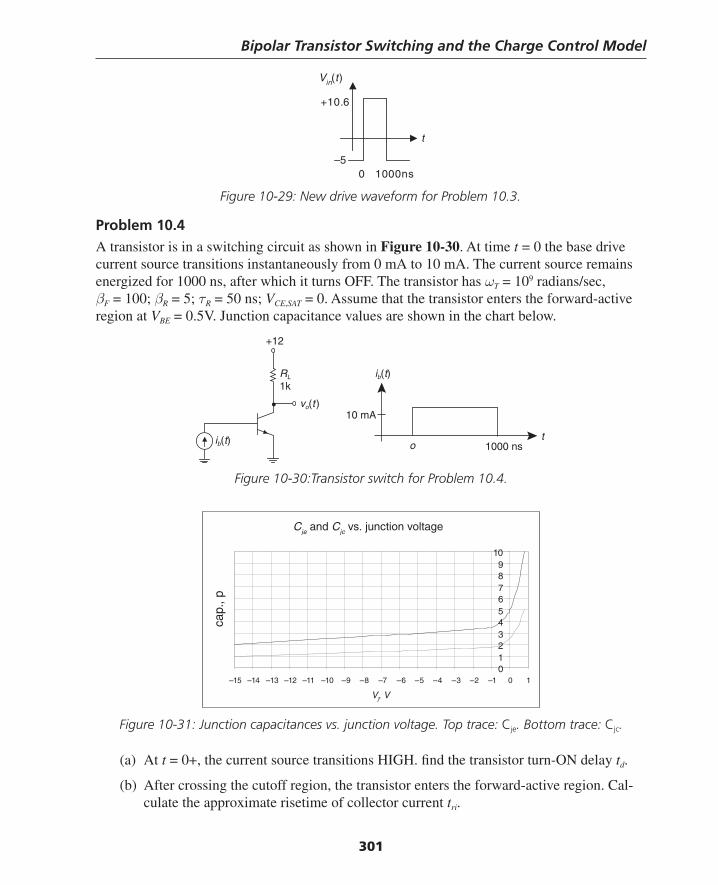
Bipolar Transistor Switching and the Charge Control Model
301
Problem 10.4A transistor is in a switching circuit as shown in Figure 10-30. At time t = 0 the base drive current source transitions instantaneously from 0 mA to 10 mA. The current source remains energized for 1000 ns, after which it turns OFF. The transistor has ωT = 109 radians/sec, βF = 100; βR = 5; τR = 50 ns; VCE,SAT = 0. Assume that the transistor enters the forward-active region at VBE = 0.5V. Junction capacitance values are shown in the chart below.
Figure 10-30:Transistor switch for Problem 10.4.
–5
+10.6
Vin(t)
t
0 1000ns
+12
ib(t) o
vo(t )
RL
1k
10 mA
ib(t)
t1000 ns
Cje and Cjc vs. junction voltage
0123456789
10
–15 –14 –13 –12 –11 –10 –9 –8 –7 –6 –5 –4 –3 –2 –1 0 1
Vj, V
cap.
, p
Figure 10-31: Junction capacitances vs. junction voltage. Top trace: Cje. Bottom trace: Cjc.
(a) At t = 0+, the current source transitions HIGH. fi nd the transistor turn-ON delay td.
(b) After crossing the cutoff region, the transistor enters the forward-active region. Cal-culate the approximate risetime of collector current tri.
Figure 10-29: New drive waveform for Problem 10.3.
Thompson Book.indb 301 3/20/2006 11:36:12 AM
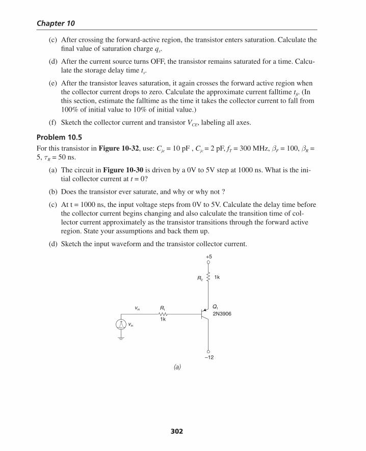
Chapter 10
302
(c) After crossing the forward-active region, the transistor enters saturation. Calculate the fi nal value of saturation charge qs.
(d) After the current source turns OFF, the transistor remains saturated for a time. Calcu-late the storage delay time ts.
(e) After the transistor leaves saturation, it again crosses the forward active region when the collector current drops to zero. Calculate the approximate current falltime tfi . (In this section, estimate the falltime as the time it takes the collector current to fall from 100% of initial value to 10% of initial value.)
(f) Sketch the collector current and transistor VCE, labeling all axes.
Problem 10.5For this transistor in Figure 10-32, use: Cje = 10 pF , Cjc = 2 pF, fT = 300 MHz, βF = 100, βR = 5, τR = 50 ns.
(a) The circuit in Figure 10-30 is driven by a 0V to 5V step at 1000 ns. What is the ini-tial collector current at t = 0?
(b) Does the transistor ever saturate, and why or why not ?
(c) At t = 1000 ns, the input voltage steps from 0V to 5V. Calculate the delay time before the collector current begins changing and also calculate the transition time of col-lector current approximately as the transistor transitions through the forward active region. State your assumptions and back them up.
(d) Sketch the input waveform and the transistor collector current.
(a)
vin R1
R2
1k
1k
+–
+5
2N3906
vin
–12
Q1
Thompson Book.indb 302 3/20/2006 11:36:12 AM
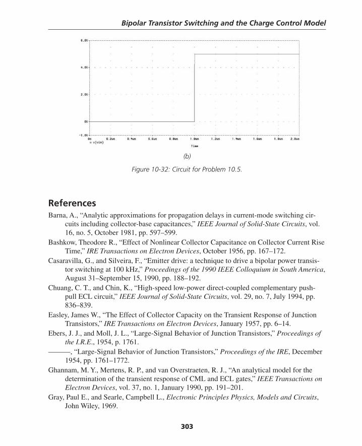
Bipolar Transistor Switching and the Charge Control Model
303
(b)
Figure 10-32: Circuit for Problem 10.5.
ReferencesBarna, A., “Analytic approximations for propagation delays in current-mode switching cir-
cuits including collector-base capacitances,” IEEE Journal of Solid-State Circuits, vol. 16, no. 5, October 1981, pp. 597–599.
Bashkow, Theodore R., “Effect of Nonlinear Collector Capacitance on Collector Current Rise Time,” IRE Transactions on Electron Devices, October 1956, pp. 167–172.
Casaravilla, G., and Silveira, F., “Emitter drive: a technique to drive a bipolar power transis-tor switching at 100 kHz,” Proceedings of the 1990 IEEE Colloquium in South America, August 31–September 15, 1990, pp. 188–192.
Chuang, C. T., and Chin, K., “High-speed low-power direct-coupled complementary push-pull ECL circuit,” IEEE Journal of Solid-State Circuits, vol. 29, no. 7, July 1994, pp. 836–839.
Easley, James W., “The Effect of Collector Capacity on the Transient Response of Junction Transistors,” IRE Transactions on Electron Devices, January 1957, pp. 6–14.
Ebers, J. J., and Moll, J. L., “Large-Signal Behavior of Junction Transistors,” Proceedings of the I.R.E., 1954, p. 1761.
———, “Large-Signal Behavior of Junction Transistors,” Proceedings of the IRE, December 1954, pp. 1761–1772.
Ghannam, M. Y., Mertens, R. P., and van Overstraeten, R. J., “An analytical model for the determination of the transient response of CML and ECL gates,” IEEE Transactions on Electron Devices, vol. 37, no. 1, January 1990, pp. 191–201.
Gray, Paul E., and Searle, Campbell L., Electronic Principles Physics, Models and Circuits, John Wiley, 1969.
Thompson Book.indb 303 3/20/2006 11:36:13 AM

Chapter 10
304
Jensen, Randall W., “Charge Control Transistor Model for the IBM Electronic Circuit Analy-sis Program,” IEEE Transactions on Circuit Theory, vol. CT-13, no. 4, December 1966, pp. 428–437.
Karadzinov, L. V., Arsov, G. L., Dzekov, T. A., and Jeffries, D. J., “Charge-control piece-wise-linear bipolar junction transistor model,” Proceedings of the IEEE International Symposium on Industrial Electronics, ISIE ’96, June 17–20, 1996, pp. 561–566.
Konstadinidis, G. K., and Berger, H. H., “Optimization of buffer stages in bipolar VLSI sys-tems,” IEEE Journal of Solid-State Circuits, vol. 27, no. 7, July 1992, pp. 1002–1013.
Kuno, H. John, “Rise and Fall Time Calculations of Junction Transistors,” IEEE Transactions on Electron Devices, April 1964, pp. 151–155.
Moll, John L., “Large-Signal Transient Response of Junction Transistors,” Proceedings of the I.R.E., December 1954, pp. 1773–1784.
Muller, Richard S., and Kamins, Theodore I., Device Electronics for Integrated Circuits, 2d edition, John Wiley, 1986.
Musumeci, S., Pagano, R., Raciti, A., Porto, C., Ronsisvalle, C., and Scollo, R., “Character-ization, parameter identifi cation and modeling of a new monolithic emitter- switching bipolar transistor,” Proceedings of the 39th Industry Applications Conference, October 3–7, 2004, pp. 1924–1931.
Neudeck, Gerold W., “The PN Junction Diode,” Modular Series on Solid State Devices, vol-ume II, Addison-Wesley, 1983.
Robinson, F. V. P., and Williams, B. W., “Optimising snubbers for high-current emitter-switched transistors,” Proceedings of the Third International Conference on Power Electronics and Variable-Speed Drives, July 13–15, 1988, pp. 177–180.
Sharaf, K. M., and Elmasry, M. I., “An accurate analytical propagation delay model for high-speed CML bipolar circuits,” IEEE Journal of Solid-State Circuits, vol. 29, no. 1, January 1994, pp. 31–45.
Stork, J. M. C., “Bipolar transistor scaling for minimum switching delay and energy dissipa-tion,” Technical Digest of International Electron Devices Meeting, December 11–14, 1988, pp. 550–553.
Thompson, M. T., and Schlecht, M. F., “High power laser diode driver based on power con-verter technology,” IEEE Transactions on Power Electronics, vol. 12, no. 1, January 1997, pp. 46–52.
Winkel, Jan TE, “Extended Charge-Control Model for Bipolar Transistors,” IEEE Transac-tions on Electron Devices, vol. ED-20, no. 4, April 1973, pp. 389–394.
Thompson Book.indb 304 3/20/2006 11:36:13 AM

305
C H A P T E R 11Review of Feedback Systems
Introduction and Some Early History of Feedback ControlA feedback system is one that compares its output to a desired input and takes corrective ac-tion to force the output to follow the input. Arguably, the beginnings of automatic feedback control1 can be traced back to the work of James Watt in the 1700s. Watt did lots of work on steam engines, and he adapted2 a centrifugal governor to automatically control the speed of a steam engine. The governor was comprised of two rotating metal balls that would fl y out due to centrifugal force. The amount of “fl y-out” was then used to regulate the speed of the steam engine by adjusting a throttle. This was an example of proportional control.
The steam engines of Watt’s day worked well with the governor, but as steam engines became larger and better engineered, it was found that there could be stability problems in the engine speed. One of the problems was hunting, or an engine speed that would surge and decrease, apparently hunting for a stable operating point. This phenomenon was not well understood until the latter part of the 19th century, when James Maxwell3 (yes, the same Maxwell famous for all those equations) developed the mathematics of the stability of the Watt governor using differential equations.
In This Chapter
The arena of “classical control system” covers single-input, single-output (SISO) linear time invariant (LTI), continuous time systems. This includes the design of classical servomechanisms and most operational amplifi er circuits. This chapter offers introductory material for the design of feedback control systems.
1 Others may argue that the origins of feedback control trace back to the water clocks and fl oat regulators of the ancients. See, e.g., Otto Mayr’s The Origins of Feedback Control, The MIT Press, 1970.
2 The centrifugal governor was invented by Thomas Mead c. 1787, for which he received British Patent #1628.
3 James C. Maxwell, “On Governors,” Proceedings of the Royal Society, 1867, pp. 270–283.
Thompson Book.indb 305 3/20/2006 11:36:13 AM
Chapter 11
306
Invention of the Negative Feedback Amplifi erWe now jump forward to the 20th century. In the early days of telephone, practical diffi cul-ties were encountered in building a transcontinental telephone line. The fi rst transcontinental telephone system, built in 1914, used #8 copper wire weighing about 1000 pounds per mile. Loss due to the resistance of the wire was approximately 60dB.4 Several vacuum tube amplifi -ers were used to boost the amplitude. These amplifi ers have limited bandwidth and signifi cant nonlinear distortion. The effects of cascading amplifi ers (Figure 11-1) resulted in intolerable amounts of signal distortion.
4 William McC. Siebert, Circuits, Signals and Systems, The MIT Press, 1986.5 Harold Black, “Inventing the Negative Feedback Amplifi er,” IEEE Spectrum, December 1977,
pp. 55–60. See also Harold Black’s U.S. Patent #2,102, 671, “Wave Translation System,” fi led April 22, 1932 and issued December 21, 1937, and Black’s early paper “Stabilized Feed-Back Amplifi ers,” Bell System Technical Journal, 1934.
Figure 11-1: Amplifi er cascade
Harold Black graduated from Worcester Polytechnic Institute in 1921 and joined Bell Labora-tory. At this time, a major task facing AT&T was the improvement of the telephone system and the problem of distortion in cascaded amplifi ers. In 1927, Black5 was considering the problem of distortion in amplifi ers and came up with the idea of the negative feedback amplifi er.
“Then came the morning of Tuesday, August 2, 1927, when the concept of the negative feedback amplifi er came to me in a fl ash while I was crossing the Hudson River on the Lacka-wanna Ferry, on the way to work. For more than 50 years I have pondered how and why the idea came, and I can’t say any more today than I could that morning. All I know is that after several years of hard work on the problem, I suddenly realized that if I fed the amplifi er output back to the input, in reverse phase, and kept the device from oscillating (singing, as we called it then), I would have exactly what I wanted: a means of canceling out the distortion in the output. I opened my morning newspaper and on a page of The New York Times I sketched a simple diagram of a negative feedback amplifi er plus the equations for the amplifi cation with feedback. I signed the sketch, and 20 minutes later, when I reached the laboratory at 463 West Street, it was witnessed, understood, and signed by the late Earl C. Bleassing.
I envisioned this circuit as leading to extremely linear amplifi ers (40 to 50dB of negative feedback), but an important question is: How did I know I could avoid self-oscillations over very wide frequency bands when many people doubted such circuits would be stable? My confi dence stemmed from work that I had done two years earlier on certain novel oscillator circuits and three years earlier in designing the terminal circuits, including the fi lters, and developing the mathematics for a carrier telephone system for short toll circuits.”
a1vi voa2 an
Thompson Book.indb 306 3/20/2006 11:36:14 AM
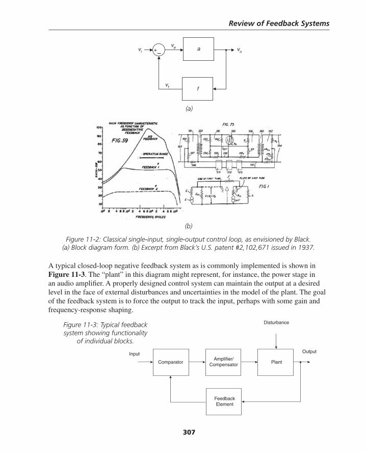
Review of Feedback Systems
307
(a)
+–avi vo
ve
vf f
(b)
Figure 11-2: Classical single-input, single-output control loop, as envisioned by Black. (a) Block diagram form. (b) Excerpt from Black’s U.S. patent #2,102,671 issued in 1937.
A typical closed-loop negative feedback system as is commonly implemented is shown in Figure 11-3. The “plant” in this diagram might represent, for instance, the power stage in an audio amplifi er. A properly designed control system can maintain the output at a desired level in the face of external disturbances and uncertainties in the model of the plant. The goal of the feedback system is to force the output to track the input, perhaps with some gain and frequency-response shaping.
ComparatorAmplifier/
Compensator Plant
FeedbackElement
Disturbance
OutputInput
Figure 11-3: Typical feedback system showing functionality
of individual blocks.
Thompson Book.indb 307 3/20/2006 11:36:14 AM
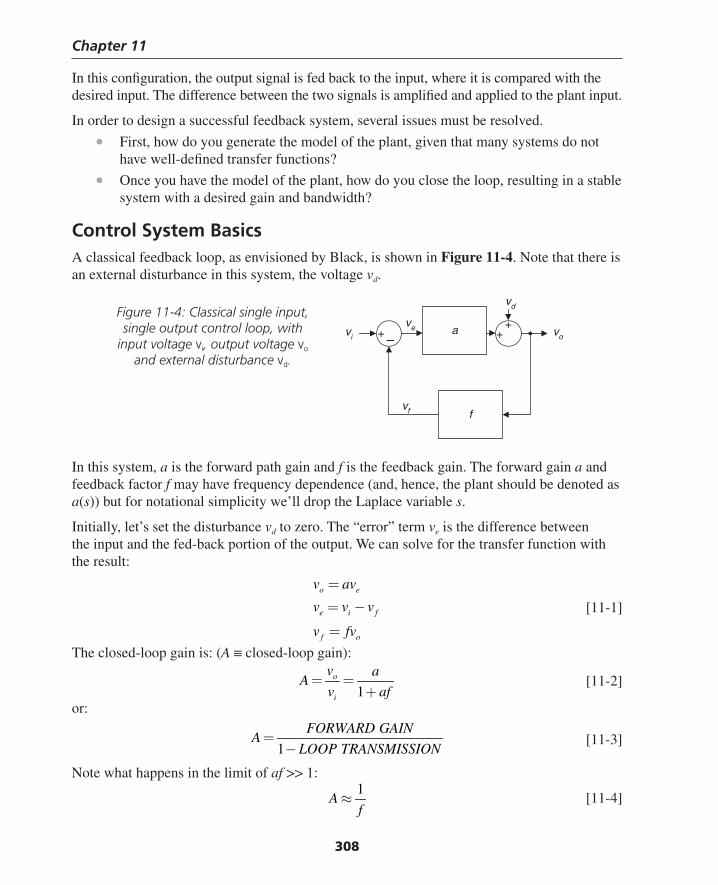
Chapter 11
308
In this confi guration, the output signal is fed back to the input, where it is compared with the desired input. The difference between the two signals is amplifi ed and applied to the plant input.
In order to design a successful feedback system, several issues must be resolved.
• First, how do you generate the model of the plant, given that many systems do not have well-defi ned transfer functions?
• Once you have the model of the plant, how do you close the loop, resulting in a stable system with a desired gain and bandwidth?
Control System BasicsA classical feedback loop, as envisioned by Black, is shown in Figure 11-4. Note that there is an external disturbance in this system, the voltage vd.
In this system, a is the forward path gain and f is the feedback gain. The forward gain a and feedback factor f may have frequency dependence (and, hence, the plant should be denoted as a(s)) but for notational simplicity we’ll drop the Laplace variable s.
Initially, let’s set the disturbance vd to zero. The “error” term ve is the difference between the input and the fed-back portion of the output. We can solve for the transfer function with the result:
o e
e i f
f o
v av
v v v
v fv
=
= −
=
[11-1]
The closed-loop gain is: (A ≡ closed-loop gain):
1
o
i
v aA
v af= =
+ [11-2]
or:
1
FORWARD GAINA
LOOP TRANSMISSION=
− [11-3]
Note what happens in the limit of af >> 1:
1
Af
≈ [11-4]
+ –avi vo
ve
vf f
vd
++
Figure 11-4: Classical single input, single output control loop, with
input voltage vi, output voltage vo and external disturbance vd.
Thompson Book.indb 308 3/20/2006 11:36:15 AM
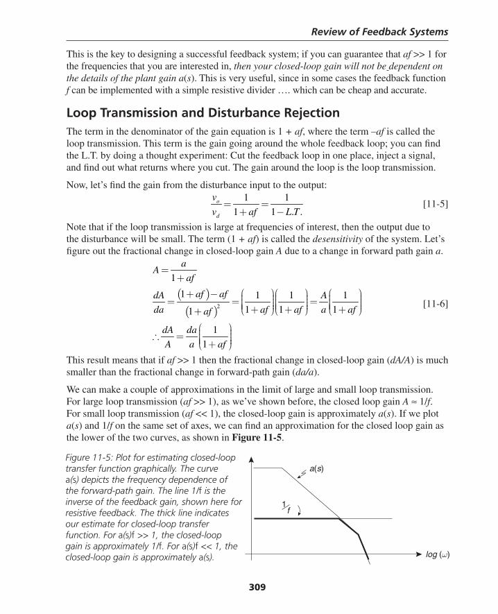
Review of Feedback Systems
309
This is the key to designing a successful feedback system; if you can guarantee that af >> 1 for the frequencies that you are interested in, then your closed-loop gain will not be dependent on the details of the plant gain a(s). This is very useful, since in some cases the feedback function f can be implemented with a simple resistive divider …. which can be cheap and accurate.
Loop Transmission and Disturbance RejectionThe term in the denominator of the gain equation is 1 + af, where the term –af is called the loop transmission. This term is the gain going around the whole feedback loop; you can fi nd the L.T. by doing a thought experiment: Cut the feedback loop in one place, inject a signal, and fi nd out what returns where you cut. The gain around the loop is the loop transmission.
Now, let’s fi nd the gain from the disturbance input to the output:
1 1
1 1 . .o
d
v
v af L T= =
+ − [11-5]
Note that if the loop transmission is large at frequencies of interest, then the output due to the disturbance will be small. The term (1 + af) is called the desensitivity of the system. Let’s fi gure out the fractional change in closed-loop gain A due to a change in forward path gain a.
( )
( )2
1
1 1 1 1
1 1 11
1
1
aA
af
af afdA A
da af af a afaf
dA da
A a af
=+
⎛ ⎞⎛ ⎞ ⎛ ⎞+ − ⎟ ⎟ ⎟⎜ ⎜ ⎜⎟ ⎟ ⎟= = =⎜ ⎜ ⎜⎟ ⎟ ⎟⎜ ⎜ ⎜⎟ ⎟ ⎟⎜ ⎜ ⎜+ + +⎝ ⎠⎝ ⎠ ⎝ ⎠+
⎛ ⎞⎟⎜ ⎟∴ = ⎜ ⎟⎜ ⎟⎜ +⎝ ⎠
[11-6]
This result means that if af >> 1 then the fractional change in closed-loop gain (dA/A) is much smaller than the fractional change in forward-path gain (da/a).
We can make a couple of approximations in the limit of large and small loop transmission. For large loop transmission (af >> 1), as we’ve shown before, the closed loop gain A ≈ 1/f. For small loop transmission (af << 1), the closed-loop gain is approximately a(s). If we plot a(s) and 1/f on the same set of axes, we can fi nd an approximation for the closed loop gain as the lower of the two curves, as shown in Figure 11-5.
log (ω)
a(s)
1f
Figure 11-5: Plot for estimating closed-loop transfer function graphically. The curve a(s) depicts the frequency dependence of the forward-path gain. The line 1/f is the inverse of the feedback gain, shown here for resistive feedback. The thick line indicates our estimate for closed-loop transfer function. For a(s)f >> 1, the closed-loop gain is approximately 1/f. For a(s)f << 1, the closed-loop gain is approximately a(s).
Thompson Book.indb 309 3/20/2006 11:36:16 AM
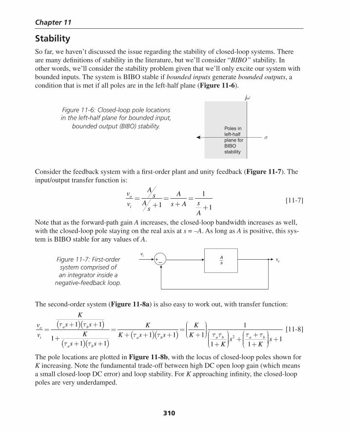
Chapter 11
310
StabilitySo far, we haven’t discussed the issue regarding the stability of closed-loop systems. There are many defi nitions of stability in the literature, but we’ll consider “BIBO” stability. In other words, we’ll consider the stability problem given that we’ll only excite our system with bounded inputs. The system is BIBO stable if bounded inputs generate bounded outputs, a condition that is met if all poles are in the left-half plane (Figure 11-6).
Figure 11-6: Closed-loop pole locations in the left-half plane for bounded input,
bounded output (BIBO) stability.
jω
σ
Poles inleft-halfplane for BIBOstability
Consider the feedback system with a fi rst-order plant and unity feedback (Figure 11-7). The input/output transfer function is:
1
1 1
o
i
Av AsA sv s A
sA
= = =++ +
[11-7]
Note that as the forward-path gain A increases, the closed-loop bandwidth increases as well, with the closed-loop pole staying on the real axis at s = –A. As long as A is positive, this sys-tem is BIBO stable for any values of A.
The second-order system (Figure 11-8a) is also easy to work out, with transfer function:
( )( )
( )( )( )( ) 2
1 1 1
1 1 11 11 1 1 1
a bo
a b a bi a b
a b
K
s sv K KKv K s s K
s ss s K K
τ ττ τ τ ττ τ
τ τ
+ + ⎛ ⎞⎟⎜= = = ⎟⎜ ⎟⎜ ⎛ ⎞ ⎛ ⎞⎝ ⎠ ++ + + + ⎟ ⎟⎜ ⎜+ + +⎟ ⎟⎜ ⎜⎟ ⎟⎟ ⎟⎜ ⎜+ + ⎝ ⎠ ⎝ ⎠+ +
[11-8]
The pole locations are plotted in Figure 11-8b, with the locus of closed-loop poles shown for K increasing. Note the fundamental trade-off between high DC open loop gain (which means a small closed-loop DC error) and loop stability. For K approaching infi nity, the closed-loop poles are very underdamped.
+–vi
voAs
Figure 11-7: First-order system comprised of an integrator inside a
negative-feedback loop.
Thompson Book.indb 310 3/20/2006 11:36:17 AM
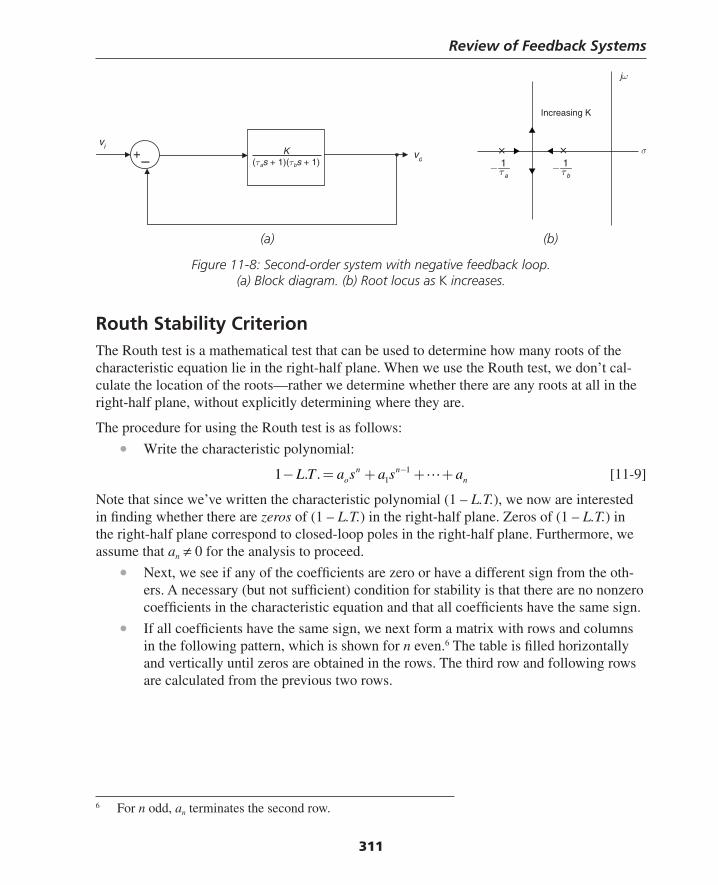
Review of Feedback Systems
311
(a) (b)
Figure 11-8: Second-order system with negative feedback loop. (a) Block diagram. (b) Root locus as K increases.
Routh Stability CriterionThe Routh test is a mathematical test that can be used to determine how many roots of the characteristic equation lie in the right-half plane. When we use the Routh test, we don’t cal-culate the location of the roots—rather we determine whether there are any roots at all in the right-half plane, without explicitly determining where they are.
The procedure for using the Routh test is as follows:
• Write the characteristic polynomial:
111 . . n n
o nL T a s a s a−− = + + + [11-9]
Note that since we’ve written the characteristic polynomial (1 – L.T.), we now are interested in fi nding whether there are zeros of (1 – L.T.) in the right-half plane. Zeros of (1 – L.T.) in the right-half plane correspond to closed-loop poles in the right-half plane. Furthermore, we assume that an ≠ 0 for the analysis to proceed.
• Next, we see if any of the coeffi cients are zero or have a different sign from the oth-ers. A necessary (but not suffi cient) condition for stability is that there are no nonzero coeffi cients in the characteristic equation and that all coeffi cients have the same sign.
• If all coeffi cients have the same sign, we next form a matrix with rows and columns in the following pattern, which is shown for n even.6 The table is fi lled horizontally and vertically until zeros are obtained in the rows. The third row and following rows are calculated from the previous two rows.
+–vi
voK
(τas + 1)(τbs + 1)
jω
σ
aτ− 1bτ− 1
× ×
Increasing K
6 For n odd, an terminates the second row.
Thompson Book.indb 311 3/20/2006 11:36:17 AM
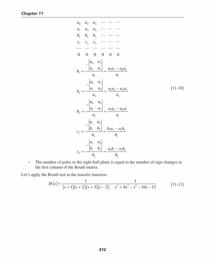
Chapter 11
312
0 2 4
1 3 5
1 2 3
1 2 3
0 2
1 3 1 2 0 31
1 1
0 4
1 5 1 4 0 52
1 1
0 6
1 7 1 6 0 73
1 1
1 3
1 2 1 3 1 21
1 1
1 5
1 3 5 1 1 32
1 1
0 0 0 0 0 0
a a a
a a a
b b b
c c c
a a
a a a a a ab
a a
a a
a a a a a ab
a a
a a
a a a a a ab
a a
a a
b b b a a bc
b b
a a
b b a b a bc
b b
−−
= =
−−
= =
−−
= =
−−
= =
−−
= =
[11-10]
• The number of poles in the right-half plane is equal to the number of sign changes in the fi rst column of the Routh matrix.
Let’s apply the Routh test to the transfer function:
( )( )( )( )( ) 4 3 2
1 1
1 2 3 2 4 16 12H s
s s s s s s s s= =
+ + + − + − − − [11-11]
Thompson Book.indb 312 3/20/2006 11:36:18 AM

Review of Feedback Systems
313
In this case, we already know that there is one right-half-plane pole at s = +2 radians/second, but we’ll use the Routh test to verify this. The Routh matrix is:
1 1 12 0
4 16 0 0
1 1 1 12 1 0
4 16 4 0 4 012 48 0 0
1 1 1
4 16 4 0
12 48 12 00 0
12 12
− −−
⎛ ⎞ ⎛ ⎞ ⎛ ⎞− −⎟ ⎟ ⎟⎜ ⎜ ⎜⎟ ⎟ ⎟− − −⎜ ⎜ ⎜⎟ ⎟ ⎟⎜ ⎜ ⎜⎟ ⎟ ⎟−⎜ ⎜ ⎜⎟ ⎟ ⎟⎜ ⎜ ⎜⎟ ⎟ ⎟= − = =⎜ ⎜ ⎜⎟ ⎟ ⎟⎟ ⎟ ⎟⎜ ⎜ ⎜− − −⎟ ⎟ ⎟⎜ ⎜ ⎜⎟ ⎟ ⎟⎜ ⎜ ⎜⎟ ⎟ ⎟⎜ ⎜ ⎜⎟ ⎟ ⎟⎟ ⎟ ⎟⎜ ⎜ ⎜⎝ ⎠ ⎝ ⎠ ⎝ ⎠⎛ ⎞ ⎛− ⎟⎜ ⎜⎟− −⎜ ⎜⎟⎜ ⎜⎟− −⎜ ⎜⎟⎜ ⎜⎟= =⎜ ⎜⎟⎟⎜ ⎜− −⎟⎜ ⎜⎟⎜ ⎜⎟⎜ ⎜⎟⎟⎜⎝ ⎠ ⎝
0 0
⎞⎟⎟⎟⎟⎟⎟⎟⎟⎟⎟⎟⎟⎟⎜ ⎠
[11-12]
We see that there is one sign change in the fi rst column, with the elements of the matrix changing from +4 to –12. Hence, there is one right-half-plane pole, as expected.
Let’s next apply the Routh test to a system with three poles inside a unity-feedback loop (Fig-ure 11-9). We’ll use the Routh test to determine the values of K that result in stable operation of this feedback loop. The closed-loop transfer function for this system is:
( )( )
( )
( )
3
3 2
3
1 1
1 3 31 11 1 11
o
i
K
v s s KKv s K s s s
K K Ks
⎛ ⎞⎟⎜ ⎟⎜ ⎟+ ⎛ ⎞⎜ ⎟⎜⎟⎜ ⎟= = ⎟⎜ ⎟⎜ ⎟⎜ ⎟⎜⎝ ⎠+ ⎟⎜ ⎟+ ⎜ + + + ⎟⎜ ⎟⎜⎝ ⎠+ + ++
[11-13]
The denominator polynomial is:
( ) 3 2 3 21 2 3
1 3 31
1 1 1oD s a s a s a s a s s sK K K
⎛ ⎞ ⎛ ⎞ ⎛ ⎞⎟ ⎟ ⎟⎜ ⎜ ⎜= + + + = + + +⎟ ⎟ ⎟⎜ ⎜ ⎜⎟ ⎟ ⎟⎜ ⎜ ⎜⎝ ⎠ ⎝ ⎠ ⎝ ⎠+ + + [11-14]
The Routh matrix is:
( )
2
2
1 3
1 1
31
1
3 181 1
01 1
1 0
0 0
K K
K
KK K
K K
⎛ ⎞ ⎛ ⎞⎟ ⎟⎜ ⎜⎟ ⎟⎜ ⎜⎟ ⎟⎜ ⎜⎝ ⎠ ⎝ ⎠+ +⎛ ⎞⎟⎜ ⎟⎜ ⎟⎜⎝ ⎠+
⎛ ⎞ ⎛ ⎞⎟ ⎟⎜ ⎜−⎟ ⎟⎜ ⎜⎟ ⎟⎜ ⎜⎝ ⎠ ⎝ ⎠ −+ + =+ +
[11-15]
Thompson Book.indb 313 3/20/2006 11:36:18 AM

Chapter 11
314
Note that if K > 8, there are two sign changes in the fi rst column. Therefore, for K = 8, we expect two poles on the jω axis and for K > 8 the system is unstable with two poles in the right-half plane. For K < 8, the system is stable with all three poles in the left-half plane.
+–vi
voK
(s + 1)3
Figure 11-9: Three poles inside unity-feedback loop.
The Phase Margin and Gain Margin TestsThe previous analyses tell us what the bandwidth and DC gain of a closed-loop system is, but doesn’t consider the question of whether a system will oscillate or have large amounts of overshoot. By using a simple Bode plot technique and a method known as the phase margin method, the relative stability of a feedback system can be determined. Phase margin is a very useful measure of the stability of a feedback system. The method for fi nding phase margin for a negative feedback system is as follows (Figure 11-10):
• Plot the magnitude and angle of the negative of the loop transmission, or –a(s)f(s).
• Find the frequency where the magnitude of a(s)f(s) drops to +1. This is the crossover frequency ωc.
• The difference between the angle at the crossover frequency and –180° is the phase margin φm.
• The gain margin (G.M.) is defi ned as the change in open-loop gain required to make the system unstable. Systems with greater gain margins can withstand greater chang-es in system parameters before becoming unstable in closed loop.
• The phase margin is defi ned as the negative change in open-loop phase shift required to make a closed-loop system unstable.
• In general, a well-designed feedback loop has a phase margin of at least 45° and a gain margin (G.M.) > 3 or so.
Thompson Book.indb 314 3/20/2006 11:36:19 AM
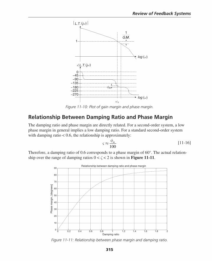
Review of Feedback Systems
315
Relationship Between Damping Ratio and Phase MarginThe damping ratio and phase margin are directly related. For a second-order system, a low phase margin in general implies a low damping ratio. For a standard second-order system with damping ratio < 0.6, the relationship is approximately:
100
mφς ≈ [11-16]
Therefore, a damping ratio of 0.6 corresponds to a phase margin of 60°. The actual relation-ship over the range of damping ratios 0 < ζ < 2 is shown in Figure 11-11.
⏐L.T. (jω)⏐
log (ω)
log (ω)
∠L.T. (jω)
1
0
−90
−180
−270
ωc
φm
..1MG
−45
−135
−225
Figure 11-10: Plot of gain margin and phase margin.
Figure 11-11: Relationship between phase margin and damping ratio.
0 0.2 0.4 0.6 0.8 1 1.2 1.4 1.6 1.8 20
10
20
30
40
50
60
70
80
90
Damping ratio
Pha
se m
argi
n, [
degr
ees]
Relationship between damping ratio and phase margin
Thompson Book.indb 315 3/20/2006 11:36:19 AM
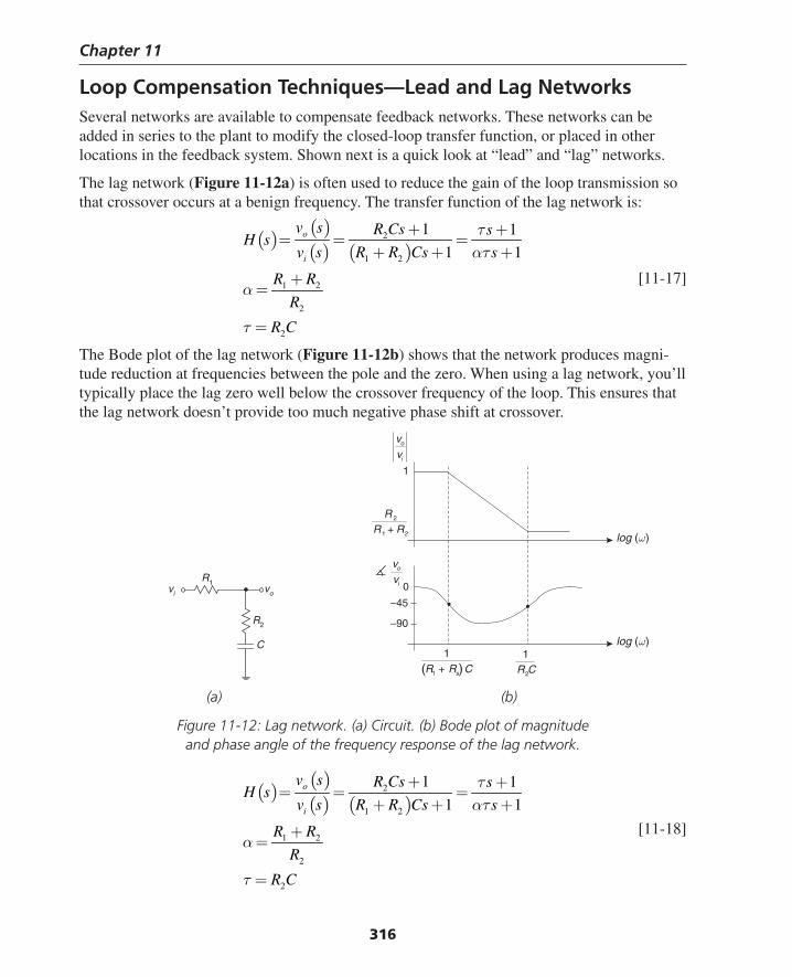
Chapter 11
316
Loop Compensation Techniques—Lead and Lag NetworksSeveral networks are available to compensate feedback networks. These networks can be added in series to the plant to modify the closed-loop transfer function, or placed in other locations in the feedback system. Shown next is a quick look at “lead” and “lag” networks.
The lag network (Figure 11-12a) is often used to reduce the gain of the loop transmission so that crossover occurs at a benign frequency. The transfer function of the lag network is:
( )( )( ) ( )
2
1 2
1 2
2
2
1 1
1 1o
i
v s R Cs sH s
v s R R Cs s
R R
R
R C
τατ
α
τ
+ += = =
+ + +
+=
=
[11-17]
The Bode plot of the lag network (Figure 11-12b) shows that the network produces magni-tude reduction at frequencies between the pole and the zero. When using a lag network, you’ll typically place the lag zero well below the crossover frequency of the loop. This ensures that the lag network doesn’t provide too much negative phase shift at crossover.
(a) (b)
Figure 11-12: Lag network. (a) Circuit. (b) Bode plot of magnitude and phase angle of the frequency response of the lag network.
( )( )( ) ( )
2
1 2
1 2
2
2
1 1
1 1o
i
v s R Cs sH s
v s R R Cs s
R R
R
R C
τατ
α
τ
+ += = =
+ + +
+=
=
[11-18]
vi vo
R1
R2
C
log (ω)
log (ω)
o
i
v
v
1
0
o
i
v
v
2
1 2
RR R+
( )1
1
sR R C+ 2
1R C
–90
–45
�
Thompson Book.indb 316 3/20/2006 11:36:20 AM
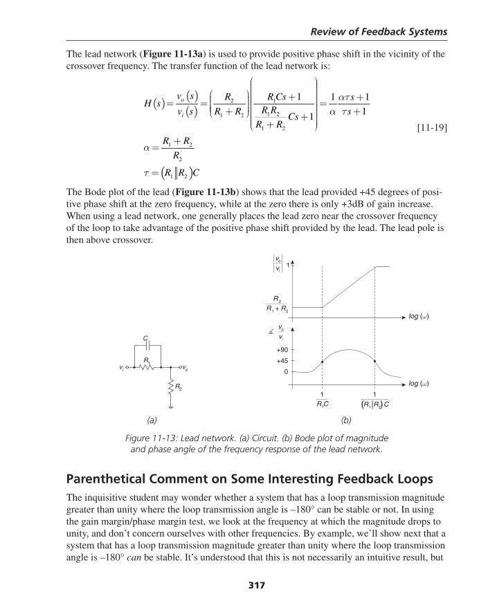
Review of Feedback Systems
317
The lead network (Figure 11-13a) is used to provide positive phase shift in the vicinity of the crossover frequency. The transfer function of the lead network is:
( )( )( )
( )
2 1
1 21 2
1 2
1 2
2
1 2
1 1 1
11
o
i
v s R R Cs sH s
R Rv s R R sCsR R
R R
R
R R C
ατα τ
α
τ
⎛ ⎞⎟⎜ ⎟⎜ ⎟⎛ ⎞⎜ + +⎟⎟⎜⎜ ⎟⎟= = =⎜⎜ ⎟⎟⎜ ⎟⎜ ⎟⎜ + +⎟⎜⎝ ⎠ ⎟⎜ + ⎟⎜ ⎟⎜ +⎝ ⎠
+=
=
[11-19]
The Bode plot of the lead (Figure 11-13b) shows that the lead provided +45 degrees of posi-tive phase shift at the zero frequency, while at the zero there is only +3dB of gain increase. When using a lead network, one generally places the lead zero near the crossover frequency of the loop to take advantage of the positive phase shift provided by the lead. The lead pole is then above crossover.
(a) (b)
Figure 11-13: Lead network. (a) Circuit. (b) Bode plot of magnitude and phase angle of the frequency response of the lead network.
Parenthetical Comment on Some Interesting Feedback LoopsThe inquisitive student may wonder whether a system that has a loop transmission magnitude greater than unity where the loop transmission angle is –180° can be stable or not. In using the gain margin/phase margin test, we look at the frequency at which the magnitude drops to unity, and don’t concern ourselves with other frequencies. By example, we’ll show next that a system that has a loop transmission magnitude greater than unity where the loop transmission angle is –180° can be stable. It’s understood that this is not necessarily an intuitive result, but
vi vo
R1
R2
C
log (ω)
o
i
v
v 1
+90
+45
0
o
i
v
v
2
1 2
RR R+
1
1R C
log (ω)
�
( )1 2
1
R R C
Thompson Book.indb 317 3/20/2006 11:36:21 AM
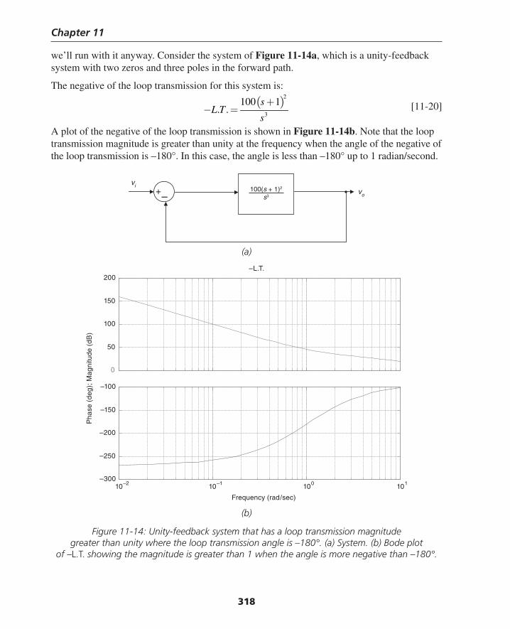
Chapter 11
318
we’ll run with it anyway. Consider the system of Figure 11-14a, which is a unity-feedback system with two zeros and three poles in the forward path.
The negative of the loop transmission for this system is:
( )2
3
100 1. .
sL T
s
+− = [11-20]
A plot of the negative of the loop transmission is shown in Figure 11-14b. Note that the loop transmission magnitude is greater than unity at the frequency when the angle of the negative of the loop transmission is –180°. In this case, the angle is less than –180° up to 1 radian/second.
(a)
+–vi
vo100(s + 1)2
s3
(b)
Figure 11-14: Unity-feedback system that has a loop transmission magnitude greater than unity where the loop transmission angle is –180°. (a) System. (b) Bode plot
of –L.T. showing the magnitude is greater than 1 when the angle is more negative than –180°.
Frequency (rad/sec)
Pha
se (
deg
); M
agni
tude
(dB
)
–L.T.
0
50
100
150
200
10–2 10–1 100 101–300
–250
–200
–150
–100
Thompson Book.indb 318 3/20/2006 11:36:21 AM
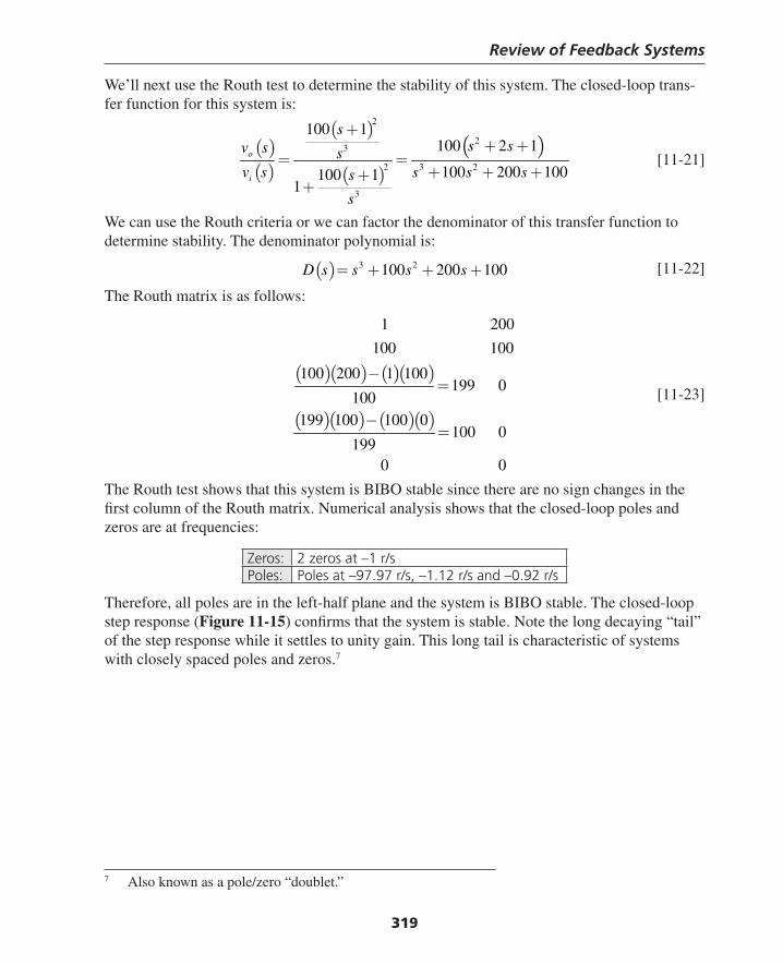
Review of Feedback Systems
319
We’ll next use the Routh test to determine the stability of this system. The closed-loop trans-fer function for this system is:
( )( )
( )
( )( )
2
23
2 3 2
3
100 1100 2 1
100 200 100100 11
o
i
ss sv s s
v s s s ss
s
++ +
= =+ + ++
+
[11-21]
We can use the Routh criteria or we can factor the denominator of this transfer function to determine stability. The denominator polynomial is:
( ) 3 2100 200 100D s s s s= + + + [11-22]
The Routh matrix is as follows:
( )( ) ( )( )
( )( ) ( )( )
1 200
100 100
100 200 1 100199 0
100199 100 100 0
100 0199
0 0
−=
−=
[11-23]
The Routh test shows that this system is BIBO stable since there are no sign changes in the fi rst column of the Routh matrix. Numerical analysis shows that the closed-loop poles and zeros are at frequencies:
Zeros: 2 zeros at –1 r/sPoles: Poles at –97.97 r/s, –1.12 r/s and –0.92 r/s
Therefore, all poles are in the left-half plane and the system is BIBO stable. The closed-loop step response (Figure 11-15) confi rms that the system is stable. Note the long decaying “tail” of the step response while it settles to unity gain. This long tail is characteristic of systems with closely spaced poles and zeros.7
7 Also known as a pole/zero “doublet.”
Thompson Book.indb 319 3/20/2006 11:36:22 AM
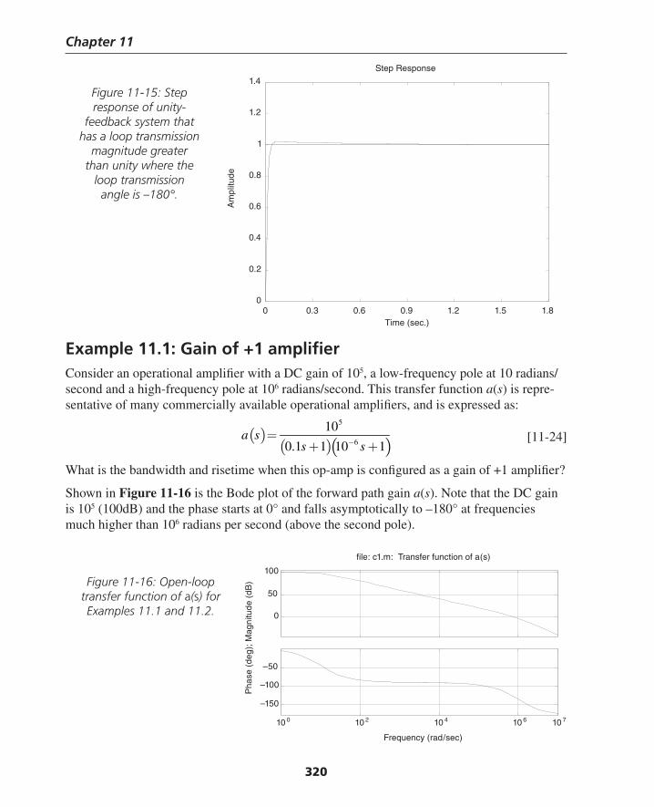
Chapter 11
320
Example 11.1: Gain of +1 amplifi erConsider an operational amplifi er with a DC gain of 105, a low-frequency pole at 10 radians/second and a high-frequency pole at 106 radians/second. This transfer function a(s) is repre-sentative of many commercially available operational amplifi ers, and is expressed as:
( )( )( )
5
6
10
0.1 1 10 1a s
s s−=
+ + [11-24]
What is the bandwidth and risetime when this op-amp is confi gured as a gain of +1 amplifi er?
Shown in Figure 11-16 is the Bode plot of the forward path gain a(s). Note that the DC gain is 105 (100dB) and the phase starts at 0° and falls asymptotically to –180° at frequencies much higher than 106 radians per second (above the second pole).
Time (sec.)
Am
plitu
de
Step Response
0 0.3 0.6 0.9 1.2 1.5 1.80
0.2
0.4
0.6
0.8
1
1.2
1.4
Time (sec.)
Figure 11-15: Step response of unity-
feedback system that has a loop transmission
magnitude greater than unity where the
loop transmission angle is –180°.
Figure 11-16: Open-loop transfer function of a(s) for Examples 11.1 and 11.2.
Frequency (rad/sec)
Pha
se (
deg)
; Mag
nitu
de (
dB)
file: c1.m: Transfer function of a(s)
0
50
100
10 0 10 2 10 4 10 6 10 7
–150
–100
–50
Thompson Book.indb 320 3/20/2006 11:36:23 AM
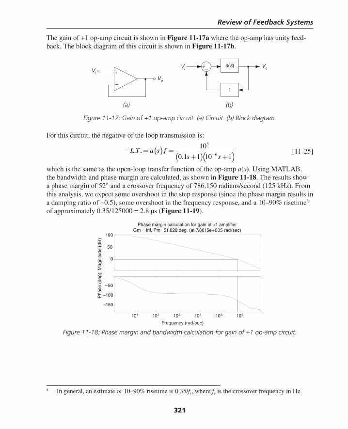
Review of Feedback Systems
321
The gain of +1 op-amp circuit is shown in Figure 11-17a where the op-amp has unity feed-back. The block diagram of this circuit is shown in Figure 11-17b.
(a) (b)
Figure 11-17: Gain of +1 op-amp circuit. (a) Circuit. (b) Block diagram.
For this circuit, the negative of the loop transmission is:
( )( )( )
5
6
10. .
0.1 1 10 1L T a s f
s s−− = =
+ + [11-25]
which is the same as the open-loop transfer function of the op-amp a(s). Using MATLAB, the bandwidth and phase margin are calculated, as shown in Figure 11-18. The results show a phase margin of 52° and a crossover frequency of 786,150 radians/second (125 kHz). From this analysis, we expect some overshoot in the step response (since the phase margin results in a damping ratio of ∼0.5), some overshoot in the frequency response, and a 10–90% risetime8 of approximately 0.35/125000 = 2.8 µs (Figure 11-19).
+
–
Vi
Vo
ViVo–+ a(s)
1
Figure 11-18: Phase margin and bandwidth calculation for gain of +1 op-amp circuit.
Frequency (rad/sec)
Pha
se (
deg)
; Mag
nitu
de (
dB)
Phase margin calculation for gain of +1 amplifierGm = Inf, Pm=51.828 deg. (at 7.8615e+005 rad/sec)
0
50
100
101 102 103 104 105 106
–150
–100
–50
8 In general, an estimate of 10–90% risetime is 0.35/fc, where fc is the crossover frequency in Hz.
Thompson Book.indb 321 3/20/2006 11:36:23 AM
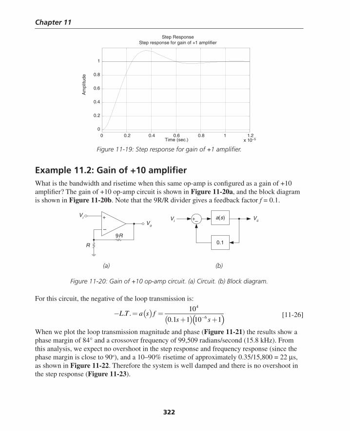
Chapter 11
322
Figure 11-19: Step response for gain of +1 amplifi er.
Example 11.2: Gain of +10 amplifi erWhat is the bandwidth and risetime when this same op-amp is confi gured as a gain of +10 amplifi er? The gain of +10 op-amp circuit is shown in Figure 11-20a, and the block diagram is shown in Figure 11-20b. Note that the 9R/R divider gives a feedback factor f = 0.1.
Time (sec.)
Am
plitu
de
Step ResponseStep response for gain of +1 amplifier
0 0.2 0.4 0.6 0.8 1 1.2x 10⁻⁵
0
0.2
0.4
0.6
0.8
1
(a) (b)
Figure 11-20: Gain of +10 op-amp circuit. (a) Circuit. (b) Block diagram.
For this circuit, the negative of the loop transmission is:
( )( )( )
4
6
10. .
0.1 1 10 1L T a s f
s s−− = =
+ + [11-26]
When we plot the loop transmission magnitude and phase (Figure 11-21) the results show a phase margin of 84° and a crossover frequency of 99,509 radians/second (15.8 kHz). From this analysis, we expect no overshoot in the step response and frequency response (since the phase margin is close to 90o), and a 10–90% risetime of approximately 0.35/15,800 = 22 μs, as shown in Figure 11-22. Therefore the system is well damped and there is no overshoot in the step response (Figure 11-23).
+
–
Vi
Vo
R
9R
ViVo–+ a(s)
0.1
Thompson Book.indb 322 3/20/2006 11:36:24 AM
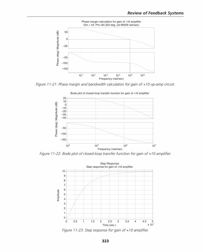
Review of Feedback Systems
323
Figure 11-22: Bode plot of closed-loop transfer function for gain of +10 amplifi er.
Frequency (rad/sec)
Pha
se (
deg)
; Mag
nitu
de (
dB)
Phase margin calculation for gain of +10 amplifierGm = Inf, Pm=84.323 deg. (at 99509 rad/sec)
–50
0
50
10 1 10 2 10 3 10 4 10 5 10 6
–150
–100
–50
Figure 11-21: Phase margin and bandwidth calculation for gain of +10 op-amp circuit.
Frequency (rad/sec)
Pha
se (
deg)
; Mag
nitu
de (
dB)
Bode plot of closed-loop transfer function for gain of +10 amplifier
–40–30–20–10
01020
104 105 106 107
–150
–100
–50
Figure 11-23: Step response for gain of +10 amplifi er.Time (sec.)
Am
plitu
de
Step ResponseStep response for gain of +10 amplifier
0 0.5 1 1.5 2 2.5 3 3.5 4 4.5 5x 10⁻⁵
0
1
2
3
4
5
6
7
8
9
10
Thompson Book.indb 323 3/20/2006 11:36:24 AM
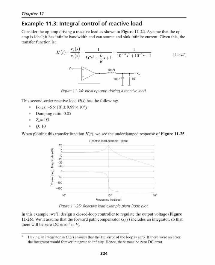
Chapter 11
324
Example 11.3: Integral control of reactive loadConsider the op-amp driving a reactive load as shown in Figure 11-24. Assume that the op-amp is ideal; it has infi nite bandwidth and can source and sink infi nite current. Given this, the transfer function is:
( )( )( ) 10 2 6
2
1 1
10 10 11
o
i
v sH s
Lv s s sLCs sR
− −= = =+ ++ +
[11-27]
Figure 11-24: Ideal op-amp driving a reactive load.
This second-order reactive load H(s) has the following:
• Poles: –5 × 10³ ± 9.99 × 10⁴ j
• Damping ratio: 0.05
• Zo = 1Ω• Q: 10
When plotting this transfer function H(s), we see the underdamped response of Figure 11-25.
+
–
Vi
Vo
10μH
1010μF
Frequency (rad/sec)
Pha
se (
deg)
; Mag
nitu
de (
dB)
Reactive load example—plant
–40–30–20–10
01020
104 105 106
–150
–100
–50
0
Figure 11-25: Reactive load example plant Bode plot.
In this example, we’ll design a closed-loop controller to regulate the output voltage (Figure 11-26). We’ll assume that the forward path compensator Gc(s) includes an integrator, so that there will be zero DC error9 in Vo.
9 Having an integrator in Gc(s) ensures that the DC error of the loop is zero. If there were an error, the integrator would forever integrate to infi nity. Hence, there must be zero DC error.
Thompson Book.indb 324 3/20/2006 11:36:25 AM
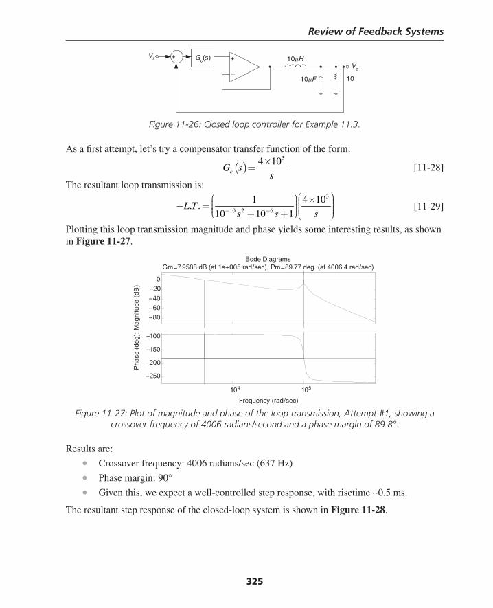
Review of Feedback Systems
325
Figure 11-26: Closed loop controller for Example 11.3.
As a fi rst attempt, let’s try a compensator transfer function of the form:
( )34 10
cG ss
×= [11-28]
The resultant loop transmission is:
3
10 2 6
1 4 10. .
10 10 1L T
ss s− −
⎛ ⎞⎛ ⎞ × ⎟⎜⎟⎜ ⎟− = ⎟⎜⎜ ⎟⎟⎜⎜ ⎟⎜⎝ ⎠+ + ⎝ ⎠ [11-29]
Plotting this loop transmission magnitude and phase yields some interesting results, as shown in Figure 11-27.
Vi −+ +
−Vo
10μH
1010μF
Gc(s)
Figure 11-27: Plot of magnitude and phase of the loop transmission, Attempt #1, showing a crossover frequency of 4006 radians/second and a phase margin of 89.8°.
Results are:
• Crossover frequency: 4006 radians/sec (637 Hz)
• Phase margin: 90°
• Given this, we expect a well-controlled step response, with risetime ∼0.5 ms.
The resultant step response of the closed-loop system is shown in Figure 11-28.
Frequency (rad/sec)
Pha
se (
deg)
; Mag
nitu
de (
dB)
Bode DiagramsGm=7.9588 dB (at 1e+005 rad/sec), Pm=89.77 deg. (at 4006.4 rad/sec)
−80
−60−40
−200
104 105
−250
−200
−150
−100
Thompson Book.indb 325 3/20/2006 11:36:26 AM
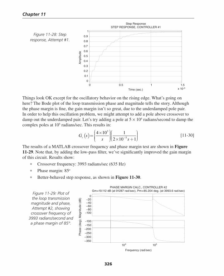
Chapter 11
326
Things look OK except for the oscillatory behavior on the rising edge. What’s going on here? The Bode plot of the loop transmission phase and magnitude tells the story. Although the phase margin is fi ne, the gain margin isn’t so great, due to the underdamped pole pair. In order to help this oscillation problem, we might attempt to add a pole above crossover to damp out the underdamped pair. Let’s try adding a pole at 5 × 10⁴ radians/second to damp the complex poles at 105 radians/sec. This results in:
( )3
5
4 10 1
2 10 1cG ss s−
⎛ ⎞⎛ ⎞× ⎟⎜ ⎟⎜⎟= ⎟⎜ ⎜⎟ ⎟⎜ ⎜⎟⎜ ⎝ ⎠× +⎝ ⎠ [11-30]
The results of a MATLAB crossover frequency and phase margin test are shown in Figure 11-29. Note that, by adding the low-pass fi lter, we’ve signifi cantly improved the gain margin of this circuit. Results show:
• Crossover frequency: 3993 radians/sec (635 Hz)
• Phase margin: 85o
• Better-behaved step response, as shown in Figure 11-30.
Time (sec.)
Am
plitu
de
Step ResponseSTEP RESPONSE, CONTROLLER #1
0 0.5 1 1.5x 10⁻³
0
0.1
0.2
0.3
0.4
0.5
0.6
0.7
0.8
0.9
1
Figure 11-29: Plot of the loop transmission magnitude and phase, Attempt #2, showing crossover frequency of
3993 radians/second and a phase margin of 85°.
Frequency (rad/sec)
Pha
se (
deg)
; Mag
nitu
de (
dB)
PHASE MARGIN CALC., CONTROLLER #2Gm=19.112 dB (at 91287 rad/sec), Pm=85.204 deg. (at 3993.6 rad/sec)
−100−80−60−40−20
0
104 105
−350−300−250−200−150−100
Figure 11-28: Step response, Attempt #1.
Thompson Book.indb 326 3/20/2006 11:36:27 AM
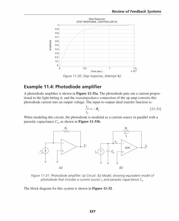
Review of Feedback Systems
327
Figure 11-30: Step response, Attempt #2.
Example 11.4: Photodiode amplifi erA photodiode amplifi er is shown in Figure 11-31a. The photodiode puts out a current propor-tional to the light hitting it, and the transimpedance connection of the op-amp converts this photodiode current into an output voltage. The input-to-output ideal transfer function is:
of
p
vR
i= − [11-31]
When modeling this circuit, the photodiode is modeled as a current source in parallel with a parasitic capacitance Cp, as shown in Figure 11-31b.
Time (sec.)
Am
plitu
de
Step ResponseSTEP RESPONSE, CONTROLLER #2
0 0.5 1 1.5x 10⁻³
0
0.1
0.2
0.3
0.4
0.5
0.6
0.7
0.8
0.9
1
(a) (b)
Figure 11-31: Photodiode amplifi er. (a) Circuit. (b) Model, showing equivalent model of photodiode that includes a current source ip and parasitic capacitance Cp.
The block diagram for this system is shown in Figure 11-32.
+
−
Rf
vo
+
−
Rf
voa(s)
ip Cp
ve
if
Thompson Book.indb 327 3/20/2006 11:36:27 AM
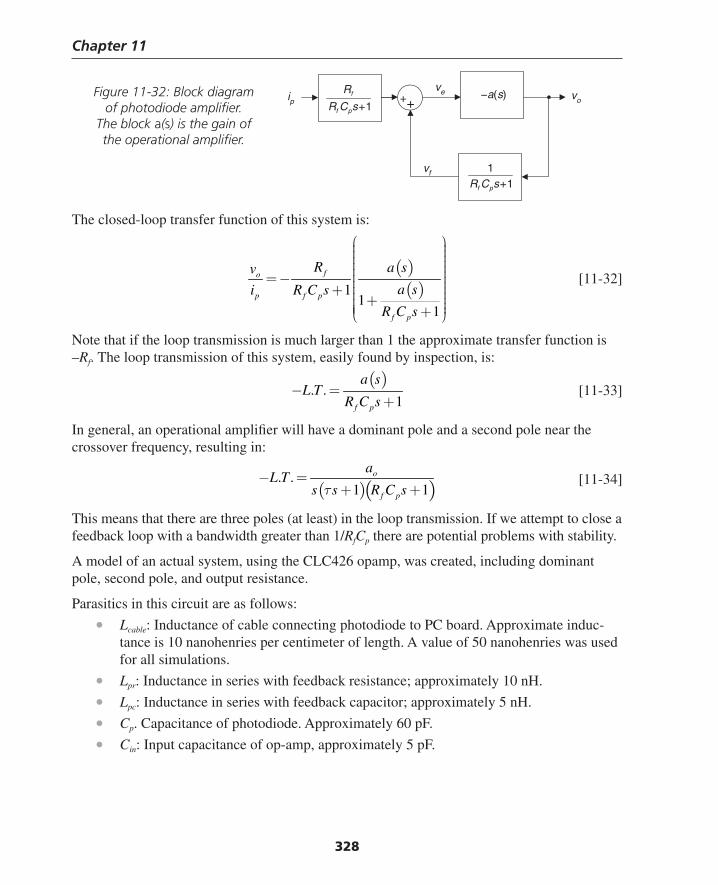
Chapter 11
328
The closed-loop transfer function of this system is:
( )
( )11
1
fo
p f p
f p
R a sv
a si R C s
R C s
⎛ ⎞⎟⎜ ⎟⎜ ⎟⎜ ⎟⎜ ⎟⎜ ⎟= − ⎜ ⎟⎟⎜+ ⎟⎜ ⎟⎜ + ⎟⎜ ⎟⎜ ⎟+⎜⎝ ⎠
[11-32]
Note that if the loop transmission is much larger than 1 the approximate transfer function is –Rf. The loop transmission of this system, easily found by inspection, is:
( )
. .1f p
a sL T
R C s− =
+ [11-33]
In general, an operational amplifi er will have a dominant pole and a second pole near the crossover frequency, resulting in:
( )( )
. .1 1
o
f p
aL T
s s R C sτ− =
+ + [11-34]
This means that there are three poles (at least) in the loop transmission. If we attempt to close a feedback loop with a bandwidth greater than 1/RfCp there are potential problems with stability.
A model of an actual system, using the CLC426 opamp, was created, including dominant pole, second pole, and output resistance.
Parasitics in this circuit are as follows:
• Lcable: Inductance of cable connecting photodiode to PC board. Approximate induc-tance is 10 nanohenries per centimeter of length. A value of 50 nanohenries was used for all simulations.
• Lpr: Inductance in series with feedback resistance; approximately 10 nH.
• Lpc: Inductance in series with feedback capacitor; approximately 5 nH.
• Cp. Capacitance of photodiode. Approximately 60 pF.
• Cin: Input capacitance of op-amp, approximately 5 pF.
++−a(s)ip vo
ve
vf
11
+sCR pf
1+sCR
R
pf
fFigure 11-32: Block diagram of photodiode amplifi er.
The block a(s) is the gain of the operational amplifi er.
Thompson Book.indb 328 3/20/2006 11:36:28 AM
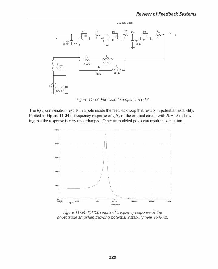
Review of Feedback Systems
329
Figure 11-33: Photodiode amplifi er model
The RfCp combination results in a pole inside the feedback loop that results in potential instability. Plotted in Figure 11-34 is frequency response of vo/ip, of the original circuit with Rf = 15k, show-ing that the response is very underdamped. Other unmodeled poles can result in oscillation.
Cin
5 pF
E1
E
E4
E
E3
E
vo2
v−
Rf Lpr
R1
C111
1 4
R2
C2
CLC425 Model
75 pF
vorout
Cp
200 pF
Ip
Cf
{cval}
Lpc
5 nH
10 nH1000Lcable
50 nH
–−++
–−++
–−++
Figure 11-34: PSPICE results of frequency response of the photodiode amplifi er, showing potential instability near 15 MHz.
Thompson Book.indb 329 3/20/2006 11:36:28 AM
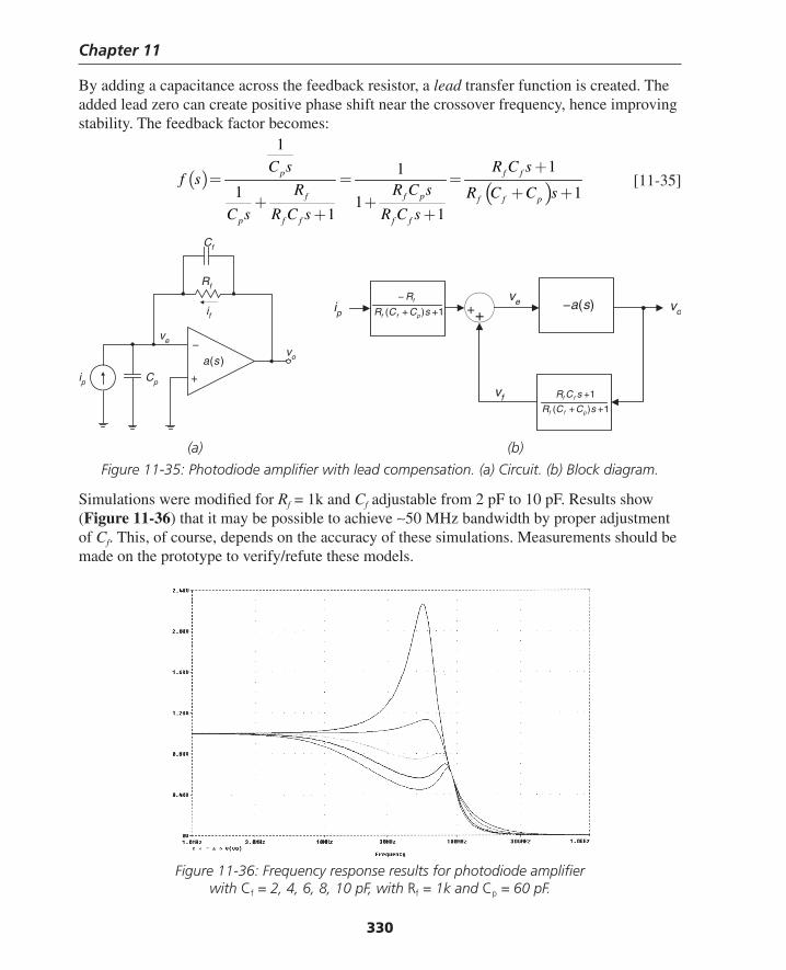
Chapter 11
330
By adding a capacitance across the feedback resistor, a lead transfer function is created. The added lead zero can create positive phase shift near the crossover frequency, hence improving stability. The feedback factor becomes:
( )( )
111
1 11
1 1
p f f
f f p f f p
p f f f f
C s R C sf s
R R C s R C C sC s R C s R C s
+= = =
+ ++ ++ +
[11-35]
(a) (b)
Figure 11-35: Photodiode amplifi er with lead compensation. (a) Circuit. (b) Block diagram.
Simulations were modifi ed for Rf = 1k and Cf adjustable from 2 pF to 10 pF. Results show (Figure 11-36) that it may be possible to achieve ∼50 MHz bandwidth by proper adjustment of Cf. This, of course, depends on the accuracy of these simulations. Measurements should be made on the prototype to verify/refute these models.
+
−
Rf
voa(s)
ip Cp
ve
if
Cf
++−a(s)ip vo
ve
vf
1)( ++
−
sCCR
R
pff
f
1)(
1
++
+
sCCR
sCR
pff
ff
Figure 11-36: Frequency response results for photodiode amplifi er with Cf = 2, 4, 6, 8, 10 pF, with Rf = 1k and Cp = 60 pF.
Thompson Book.indb 330 3/20/2006 11:36:30 AM
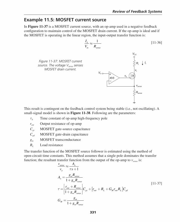
Review of Feedback Systems
331
Example 11.5: MOSFET current sourceIn Figure 11-37 is a MOSFET current source, with an op-amp used in a negative feedback confi guration to maintain control of the MOSFET drain current. If the op-amp is ideal and if the MOSFET is operating in the linear region, the input-output transfer function is:
1L
in sense
I
V R≈ [11-36]
IL
VCC
RL
vL
vsense
Rsense
va
Vin +
−a(s)
This result is contingent on the feedback control system being stable (i.e., not oscillating). A small-signal model is shown in Figure 11-38. Following are the parameters:
τh Time constant of op-amp high-frequency pole
rout Output resistance of op-amp
Cgs MOSFET gate-source capacitance
Cgd MOSFET gate-drain capacitance
gm MOSFET transconductance
RL Load resistance
The transfer function of the MOSFET source follower is estimated using the method of open-circuit time constants. This method assumes that a single pole dominates the transfer function; the resultant transfer function from the output of the op-amp to vsense is:
[ ]
1
1
1
1
sense o
a
m senseo
m sense
out sensegs out L M out L gd
m sense
mM
m sense
v A
v s
g RA
g R
r RC r R G r R C
g R
gG
g R
τ
τ
≈+
=+
⎡ ⎤+⎢ ⎥= + + +⎢ ⎥+⎣ ⎦
=+
[11-37]
Figure 11-37: MOSFET current source. The voltage Vsense senses
MOSFET drain current.
Thompson Book.indb 331 3/20/2006 11:36:31 AM
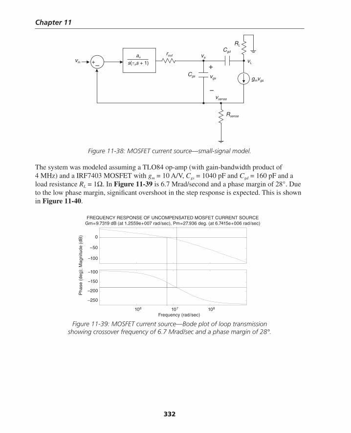
Chapter 11
332
Figure 11-38: MOSFET current source—small-signal model.
The system was modeled assuming a TLO84 op-amp (with gain-bandwidth product of 4 MHz) and a IRF7403 MOSFET with gm = 10 A/V, Cgs = 1040 pF and Cgd = 160 pF and a load resistance RL = 1Ω. In Figure 11-39 is 6.7 Mrad/second and a phase margin of 28°. Due to the low phase margin, signifi cant overshoot in the step response is expected. This is shown in Figure 11-40.
+–
ao
s(τhs + 1)vin
+
−
rout va
Cgs
Cgd
vgs
vsense
Rsense
RL
vL
gmvgs
Frequency (rad/sec)
Pha
se (
deg)
; Mag
nitu
de (
dB)
FREQUENCY RESPONSE OF UNCOMPENSATED MOSFET CURRENT SOURCEGm=9.7319 dB (at 1.2559e+007 rad/sec), Pm=27.936 deg. (at 6.7415e+006 rad/sec)
−100
−50
0
106 107 108
−250
−200
−150
−100
Figure 11-39: MOSFET current source—Bode plot of loop transmission showing crossover frequency of 6.7 Mrad/sec and a phase margin of 28°.
Thompson Book.indb 332 3/20/2006 11:36:31 AM
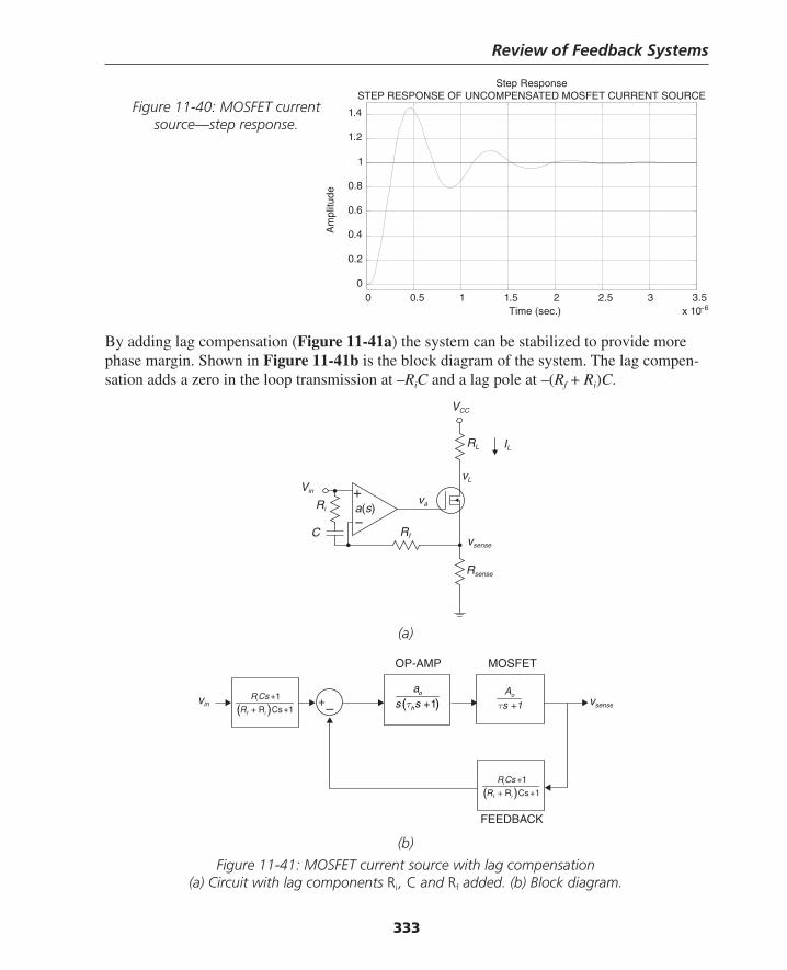
Review of Feedback Systems
333
By adding lag compensation (Figure 11-41a) the system can be stabilized to provide more phase margin. Shown in Figure 11-41b is the block diagram of the system. The lag compen-sation adds a zero in the loop transmission at –RiC and a lag pole at –(Rf + Ri)C.
(a)
Time (sec.)
Am
plitu
de
Step ResponseSTEP RESPONSE OF UNCOMPENSATED MOSFET CURRENT SOURCE
0 0.5 1 1.5 2 2.5 3 3.5x 10⁻⁶
0
0.2
0.4
0.6
0.8
1
1.2
1.4
IL
VCC
RL
vL
vsense
Rsense
va
Vin +
−a(s)
Rf
Ri
C
+–vin ( )
1
+1i
f i
R Cs
R + R Cs
+
OP-AMP MOSFET
( )1o
h
a
s sτ +
( )1
+1i
f i
R Cs
R + R Cs
+
1oA
sτ +
FEEDBACK
vsense
(b)
Figure 11-41: MOSFET current source with lag compensation (a) Circuit with lag components Ri , C and Rf added. (b) Block diagram.
Figure 11-40: MOSFET current source—step response.
Thompson Book.indb 333 3/20/2006 11:36:32 AM

Chapter 11
334
Example 11.6: Maglev exampleMaglev10 systems using superconducting magnets in the magnetic suspension have low damping. Furthermore, it has been demonstrated that these electrodynamic suspensions (EDS) may have slightly negative damping under certain operating conditions (with poles in the right-half plane). Therefore, a control system is needed to prevent underdamped or unstable vertical oscillations.
In order to suspend the magnet statically, the downward gravitational pull is canceled by an upward magnetic force. The magnet is levitated stably; that is, a deviation from the equilib-rium position results in a restoring force, similar to a mass and a spring. In an electromagnetic suspension (such as a steel ball suspended in a magnetic fi eld) there is no stable equilibrium for DC excitation of the magnet.
The magnetic levitating force acting on the magnet is given by:
2Z m Mf k z Ci z= − = − [11-38]
where km is the equivalent spring constant, z is the vertical distance with reference to the mag-net null position, iM is magnet current, and C is a constant that accounts for magnet and coil geometry and relative velocity between the magnet and levitating coils.
Step response results for the resultant system with the following parameters are shown in Figure 11-42.
• Ri = 47k
• Rf = 470k
• C = 1000 pF
Note that the system has a better-behaved step response, with no overshoot, but that the 10–90% risetime has signifi cantly increased as compared to the uncompensated case.
Time (sec.)
Am
plitu
de
Step ResponseSTEP RESPONSE OF LAG COMPENSATED MOSFET CURRENT SOURCE
0 0.5 1 1.5 2 2.5x 10⁻⁵
0
0.1
0.2
0.3
0.4
0.5
0.6
0.7
0.8
0.9
1
10 “Maglev” is a term used generically for a number of systems utilizing magnetic suspensions for ground transportation. Currently (2004) there is one revenue-producing Maglev system operating in China, and others are proposed.
Figure 11-42: MOSFET current source with lag compensation,
step response.
Thompson Book.indb 334 3/20/2006 11:36:32 AM
Review of Feedback Systems
335
Assuming that there are incremental changes in forces, magnet vertical position, and magnet currents, a linearized model can be generated relating incremental changes in magnet vertical position to changes in incremental magnet current. Vertical force, vertical position and mag-net current are given as the sum of a DC component and an incremental component:
Z Z z
o
M M m
f F f
z Z z
i I i
= +
= +
= +
[11-39]
Putting this into the force equation results in:
2 2 2Z M o M M o mf CI Z CI z CI Z i≈ − − − [11-40]
where second-order and higher terms have been neglected. At equilibrium, there is a resultant magnetic force that balances the force of gravity:
2Z M oF Mg CI Z= = − [11-41]
Newton’s law applied to the magnet results in:
2
22
2M M M o
d zM f Mg CI z CI Z i
dt= − = − − [11-42]
resulting in:
2
2 2
2m
m MM
M d z Mgz i
k ICI dt+ = [11-43]
Using the spring constant k, and converting the equation to the frequency domain results in:
( ) ( )2 21 m
m m M
M Mgs z s i s
k k I
⎛ ⎞⎟⎜ ⎟+ =⎜ ⎟⎜ ⎟⎜⎝ ⎠ [11-44]
resulting in the transfer function between magnet position and magnet control current:
( )( ) 2
2
1mm M
m
z s Mg
i s Mk I s
k
=⎛ ⎞⎟⎜ ⎟+⎜ ⎟⎜ ⎟⎜⎝ ⎠
[11-45]
This result shows that this suspension has two jω-axis poles, as in a simple, lossless mass-spring system:
1,2
mp
ks j
M= ± [11-46]
Such a system can have the closed-loop poles arbitrarily adjusted by applying position-veloc-ity. By adjusting the parameters Kf, Kv, and Kp the poles can be placed in the left-half plane with suffi cient damping to achieve good ride quality.
Thompson Book.indb 335 3/20/2006 11:36:33 AM
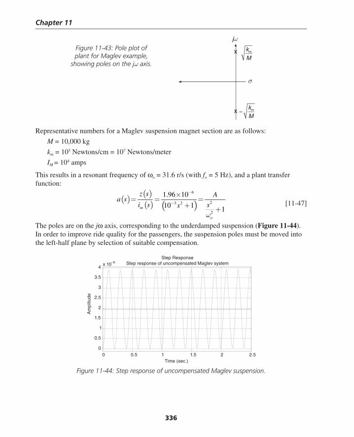
Chapter 11
336
Representative numbers for a Maglev suspension magnet section are as follows:
M = 10,000 kg
km = 105 Newtons/cm = 107 Newtons/meter
IM = 104 amps
This results in a resonant frequency of ωo = 31.6 r/s (with fo = 5 Hz), and a plant transfer function:
( )( )( ) ( )
6
23 2
2
1.96 10
10 1 1m
o
z s Aa s
i s ssω
−
−
×= = =
+ + [11-47]
The poles are on the jω axis, corresponding to the underdamped suspension (Figure 11-44). In order to improve ride quality for the passengers, the suspension poles must be moved into the left-half plane by selection of suitable compensation.
Figure 11-44: Step response of uncompensated Maglev suspension.
mk
M−
mk
M
σ
jω
x
x
Time (sec.)
Am
plitu
de
Step ResponseStep response of uncompensated Maglev system
0 0.5 1 1.5 2 2.50
0.5
1
1.5
2
2.5
3
3.5
4x 10⁻⁶
Figure 11-43: Pole plot of plant for Maglev example,
showing poles on the jω axis.
Thompson Book.indb 336 3/20/2006 11:36:34 AM
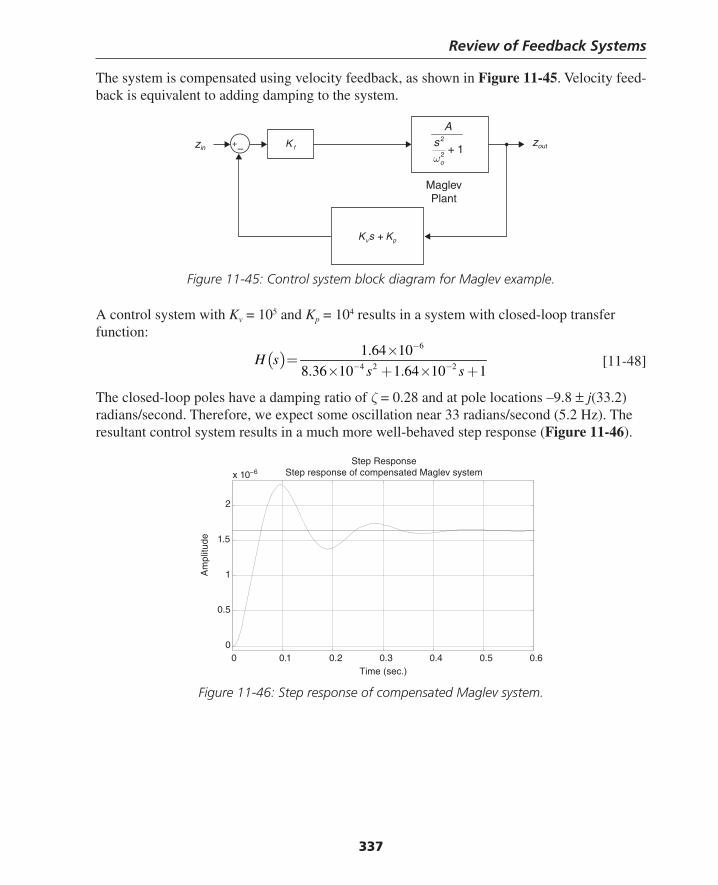
Review of Feedback Systems
337
The system is compensated using velocity feedback, as shown in Figure 11-45. Velocity feed-back is equivalent to adding damping to the system.
Figure 11-45: Control system block diagram for Maglev example.
A control system with Kv = 105 and Kp = 104 results in a system with closed-loop transfer function:
( )6
4 2 2
1.64 10
8.36 10 1.64 10 1H s
s s
−
− −
×=
× + × + [11-48]
The closed-loop poles have a damping ratio of ζ = 0.28 and at pole locations –9.8 ± j(33.2) radians/second. Therefore, we expect some oscillation near 33 radians/second (5.2 Hz). The resultant control system results in a much more well-behaved step response (Figure 11-46).
Figure 11-46: Step response of compensated Maglev system.
zoutzin +–
MaglevPlant
v pK s K+
fK 2
2 1o
Asω
+
Time (sec.)
Am
plitu
de
Step ResponseStep response of compensated Maglev system
0 0.1 0.2 0.3 0.4 0.5 0.60
0.5
1
1.5
2
x 10−6
Thompson Book.indb 337 3/20/2006 11:36:34 AM

Chapter 11
338
Appendix: MATLAB Scripts
MATLAB script for gain of +1 and +10 amplifi ersfunction c1
% Control system example #1
% Calculates parameters for gain of +1 and gain of +10 amplifi ers
% Marc Thompson, 10/22/99
% Open loop transfer function a(s)
ao=1e5; % DC gain
d=conv([0.1 1],[1e-6 1]); % Poles
a=tf(ao,d); % Create transfer function a(s)
bode(a) % Plot Bode plot of a(s)
title(‘fi le: c1.m: Transfer function of a(s)’)
fi gure;
pzmap(a); % Plot pole/zero map of a(s)
title(‘fi le: c1.m: Pole map of a(s)’);
damp(a) % Find natural frequency and damping ratio of
a(s)
% gain of +1
f=1; % Feedback gain of +1
margin(a*f) % Find phase and gain margin
title(‘Phase margin calculation for gain of +1 amplifi er’);fi gure;
f=tf(f,1); % Create feedback f(s)
cloop=feedback(a,f) % Close the loop, fi nd transfer function H(s)
bode(cloop)
title(‘Bode plot of closed-loop transfer function for gain of +1
amplifi er’);fi gure
step(cloop)
title(‘Step response for gain of +1 amplifi er’);grid;fi gure
pzmap(cloop)
title(‘Pole map of closed-loop gain of +1 amplifi er’);grid;fi gure;
damp(cloop) % Find natural frequency and damping ratio of
H(s)
% gain of +10
f=0.1;
margin(ao*f,d);title(‘Phase margin calculation for gain of +10
amplifi er’);fi gure;
f=tf(f,1);
cloop=feedback(a,f);cloopgainof10=cloop
bode(cloop);title(‘Bode plot of closed-loop transfer function for gain of
+10 amplifi er’);fi gure
step(cloop);grid;title(‘Step response for gain of +10 amplifi er’);
pzmap(cloop);title(‘Pole map of closed-loop gain of +10 amplifi er’);grid;
damp(cloop)
Thompson Book.indb 338 3/20/2006 11:36:35 AM

Review of Feedback Systems
339
MATLAB script for integral control examplefunction c3
% Control example 3
% driving reactive load
L=10e-6;
C=10e-6;
R=10;
Zo = sqrt(L/C); % Characteristic Impedance
Q=R/Zo
% Calculate PLANT
num=1;
denom=[L*C L/R 1];
plant=tf(num,denom)
damp(plant) % Find poles and damping ratio
bode(plant); title(‘fi le: c3.m; REACTIVE LOAD EXAMPLE’)
% Integral control, attempt #1
Gain=4e3; % Integrator gain
denom=[1 0];
Gc=tf(Gain,denom); % Form Gc(s)
Forw=series(plant,Gc); % Cascade with plant
margin(Forw); % Find gain and phase margin
F=tf(1,1);
Cloop=feedback(Forw,F,-1)
fi gure; step(Cloop);title(‘STEP RESPONSE, CONTROLLER #1’);grid
%Integral control, attempt #2
fi gure
d=[1/5e4 1];
LPF=tf(1,d); % Add lowpass fi lter to damp complex pole pair
Gc=series(LPF,Gc);
Forw=series(plant,Gc);
margin(Forw); title(‘PHASE MARGIN CALC., CONTROLLER #2’);
F=tf(1,1);
Cloop=feedback(Forw,F,-1)
fi gure; step(Cloop);title(‘STEP RESPONSE, CONTROLLER #2’);grid
Thompson Book.indb 339 3/20/2006 11:36:35 AM

Chapter 11
340
MATLAB script for MOSFET current source examplefunction moscursource
% Analysis of MOSFET current source
% Marc Thompson, 3/28/00
% LOAD
RL=1;
% MOSFET model
gm = 8.6; % transconductance
Cgs = 1040e-12;
Cgd = 160e-12;
% OPAMP model
rout = 100; % output resistance of opamp
ao=2*pi*4*1e6; % GBP = 4 MHz
denom=[1/ao 0];
highpole=[1/ao 1];
d=conv(denom,highpole);
opamp=tf(1,d)
% MOSFET follower model
Rsense = 0.08; % current sense resistor
Ao=gm*Rsense/(1+gm*Rsense); % gain of follower
% MOSFET OCTC calculation
Rgs=(rout+Rsense)/(1+gm*Rsense);
Tgs=Rgs*Cgs;
GM=gm/(1+gm*Rsense);
Rgd=rout+RL+(GM*rout*RL);
Tgd=Rgd*Cgd;
T=Tgs+Tgd % sum of OCTCs
mosfetpole=1/T
mosfet=tf(Ao,[T 1])
% Find loop transmission
LT=series(opamp,mosfet)
margin(LT);
title(‘moscursource. FREQUENCY RESPONSE OF UNCOMPENSATED MOSFET CURRENT
SOURCE’)
fi gure;
% close the loop
f=tf(1,1)
uncomp=feedback(LT,f,-1);
step(uncomp); grid;
Thompson Book.indb 340 3/20/2006 11:36:35 AM

Review of Feedback Systems
341
title(‘moscursource. STEP RESPONSE OF UNCOMPENSATED MOSFET CURRENT SOURCE’)
fi gure
% add lag compensation
Rf=470000; C=1e-9;
Ri=47000;
numlag=[Ri*C 1];
denomlag=[(Ri+Rf)*C 1];
f=tf(numlag,denomlag)
comp=feedback(LT,f,-1);
comp=series(f,comp);
step(comp); grid;
title(‘moscursource. STEP RESPONSE OF LAG COMPENSATED MOSFET CURRENT
SOURCE’)
MATLAB script for Maglev examplefunction maglev
% Maglev example
% Marc Thompson 4/3/00
% Maglev plant
wn=sqrt(1e3);
num=1.96e-6;
denom=[1/wn^2 0 1];
plant=tf(num,denom);
step(plant);
title(‘Step response of uncompensated Maglev system’);grid;
fi gure
% feedback compensation
Kp=1e5;
Kv=1e4;
num=[Kv Kp];
f=tf(num,1);
% Closed-loop
sys=feedback(plant,f,-1)
damp(sys)
step(sys);
grid;
title(‘Step response of compensated Maglev system’)
Thompson Book.indb 341 3/20/2006 11:36:35 AM
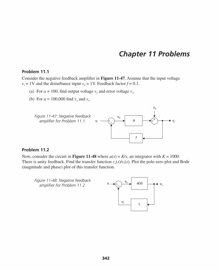
342
Chapter 11 Problems
Problem 11.1Consider the negative feedback amplifi er in Figure 11-47. Assume that the input voltage vi = 1V and the disturbance input vd = 1V. Feedback factor f = 0.1.
(a) For a = 100, fi nd output voltage vo and error voltage ve.
(b) For a = 100,000 fi nd vo and ve.
++a
f
vo
vd
ve
vi +–
a(s) vo
vf
vevi +–
1
Figure 11-47: Negative feedback amplifi er for Problem 11.1.
Problem 11.2 Now, consider the circuit in Figure 11-48 where a(s) = K/s, an integrator with K = 1000. There is unity feedback. Find the transfer function vo(s)/vi(s). Plot the pole-zero plot and Bode (magnitude and phase) plot of this transfer function.
Figure 11-48: Negative feedback amplifi er for Problem 11.2.
Thompson Book.indb 342 3/20/2006 11:36:35 AM
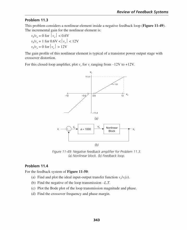
Review of Feedback Systems
343
Problem 11.3This problem considers a nonlinear element inside a negative feedback loop (Figure 11-49). The incremental gain for the nonlinear element is:
vb/va = 0 for ⏐va⏐ < 0.6V
vb/va = 1 for 0.6V <⏐va⏐ < 12V
vb/va = 0 for⏐va⏐ > 12V
The gain profi le of this nonlinear element is typical of a transistor power output stage with crossover distortion.
For this closed-loop amplifi er, plot vo for vi ranging from –12V to +12V.
(a)
(b)
Figure 11-49: Negative feedback amplifi er for Problem 11.3. (a) Nonlinear block. (b) Feedback loop.
Problem 11.4For the feedback system of Figure 11-50:
(a) Find and plot the ideal input-output transfer function vo/vi(s).
(b) Find the negative of the loop transmission –L.T.
(c) Plot the Bode plot of the loop transmission magnitude and phase.
(d) Find the crossover frequency and phase margin.
vo
vavevi a = 1000 NonlinearBlock
= 1.0
12va
vo
11.4
0.6−0.6−12
−11.4
+–
Thompson Book.indb 343 3/20/2006 11:36:36 AM
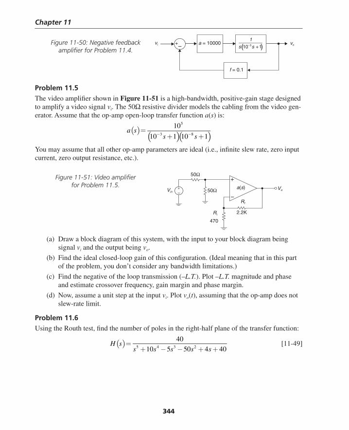
Chapter 11
344
Problem 11.5The video amplifi er shown in Figure 11-51 is a high-bandwidth, positive-gain stage designed to amplify a video signal vi. The 50Ω resistive divider models the cabling from the video gen-erator. Assume that the op-amp open-loop transfer function a(s) is:
( )( )( )
5
3 8
10
10 1 10 1a s
s s− −=
+ +
You may assume that all other op-amp parameters are ideal (i.e., infi nite slew rate, zero input current, zero output resistance, etc.).
(a) Draw a block diagram of this system, with the input to your block diagram being signal vi and the output being vo.
(b) Find the ideal closed-loop gain of this confi guration. (Ideal meaning that in this part of the problem, you don’t consider any bandwidth limitations.)
(c) Find the negative of the loop transmission (–L.T.). Plot –L.T. magnitude and phase and estimate crossover frequency, gain margin and phase margin.
(d) Now, assume a unit step at the input vi. Plot vo(t), assuming that the op-amp does not slew-rate limit.
Problem 11.6Using the Routh test, fi nd the number of poles in the right-half plane of the transfer function:
( ) 5 4 3 2
40
10 5 50 4 40H s
s s s s s=
+ − − + + [11-49]
Figure 11-51: Video amplifi er for Problem 11.5.
vi a = 10000+– ( )3
1
10 1s s− +
f = 0.1
vo
Vin
+
−
a(s)
Rf
Vo
Ri
470
2.2K
50Ω
50Ω
+–
Figure 11-50: Negative feedback amplifi er for Problem 11.4.
Thompson Book.indb 344 3/20/2006 11:36:36 AM
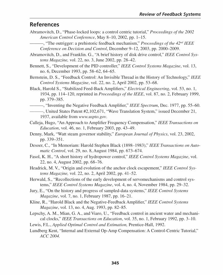
Review of Feedback Systems
345
ReferencesAbramovitch, D., “Phase-locked loops: a control centric tutorial,” Proceedings of the 2002
American Control Conference, May 8–10, 2002, pp. 1–15.———, “The outrigger: a prehistoric feedback mechanism,” Proceedings of the 42nd IEEE
Conference on Decision and Control, December 9–12, 2003, pp. 2000–2009.Abramovitch, D., and Franklin. G., “A brief history of disk drive control,” IEEE Control Sys-
tems Magazine, vol. 22, no. 3, June 2002, pp. 28–42.Bennett, S., “Development of the PID controller,” IEEE Control Systems Magazine, vol. 13,
no. 6, December 1993, pp. 58–62, 64–65.Bernstein, D. S., “Feedback Control: An Invisible Thread in the History of Technology,” IEEE
Control Systems Magazine, vol. 22, no. 2, April 2002, pp. 53–68.Black, Harold S., “Stabilized Feed-Back Amplifi ers,” Electrical Engineering, vol. 53, no. 1,
1934, pp. 114–120, reprinted in Proceedings of the IEEE, vol. 87, no. 2, February 1999, pp. 379–385.
———, “Inventing the Negative Feedback Amplifi er,” IEEE Spectrum, Dec. 1977, pp. 55–60.———, United States Patent #2,102,671, “Wave Translation System,” issued December 21,
1937, available from www.uspto.gov. Calleja, Hugo, “An Approach to Amplifi er Frequency Compensation,” IEEE Transactions on
Education, vol. 46, no. 1, February 2003, pp. 43–49.Denny, Mark, “Watt steam governor stability,” European Journal of Physics, vol. 23, 2002,
pp. 339–351.Desoer, C., “In Memoriam: Harold Stephen Black (1898–1983),” IEEE Transactions on Auto-
matic Control, vol. 29, no. 8, August 1984, pp. 673–674.Fasol, K. H., “A short history of hydropower control,” IEEE Control Systems Magazine, vol.
22, no. 4, August 2002, pp. 68–76.Headrick, M. V., “Origin and evolution of the anchor clock escapement,” IEEE Control Sys-
tems Magazine, vol. 22, no. 2, April 2002, pp. 41–52.Herwald, S., “Recollections of the early development of servomechanisms and control sys-
tems,” IEEE Control Systems Magazine, vol. 4, no. 4, November 1984, pp. 29–32.Jury, E., “On the history and progress of sampled-data systems,” IEEE Control Systems
Magazine, vol. 7, no. 1, February 1987, pp. 16–21.Kline, R., “Harold Black and the Negative-Feedback Amplifi er,” IEEE Control Systems
Magazine, vol. 13, no. 4, Aug. 1993, pp. 82–85.Lepschy, A. M., Mian, G. A., and Viaro, U., “Feedback control in ancient water and mechani-
cal clocks,” IEEE Transactions on Education, vol. 35, no. 1, February 1992, pp. 3–10.Lewis, F.L., Applied Optimal Control and Estimation, Prentice-Hall, 1992.Lundberg Kent, “Internal and External Op-Amp Compensation: A Control-Centric Tutorial,”
ACC 2004.
Thompson Book.indb 345 3/20/2006 11:36:37 AM
Chapter 11
346
Lundberg, Kent H., and Roberge, James K.. “Classical Dual-Inverted-Pendulum Control,” Proceeding of the IEEE CDC 2003, pp. 4399–4404, December 9–12, 2003, Maui, Hawaii.
Mancini, Ron, “The Saga of Harry Black,” EDN Magazine, March 15, 2001, p. 34.Maxwell, James C., “On Governors,” Proceedings of the Royal Society, 1867, pp. 270–283.Mayr, Otto, The Origins of Feedback Control, The MIT Press, 1970.Michel, A. N., “Stability: the common thread in the evolution of feedback control,” IEEE
Control Systems Magazine, vol. 16, no. 3, June 1996, pp. 50–60.Pidhayny, D., “The origins of feedback control,” IEEE Transactions on Automatic Control,
vol. 17, no. 2, April 1972, pp. 283–284.Roberge, James K., Operational Amplifi ers: Theory and Practice, John Wiley, 1975.Siebert, William McC., Circuits, Signals and Systems, The MIT Press, 1986.Tilbury, Dawn, Luntz, Jonathan, and Messner, William, “Controls Education on the WWW:
Tutorials for MATLAB and Simulink,” Proceedings of the American Control Confer-ence, Philadelphia PA, June 1998, pp. 1304–1308.
Thompson Book.indb 346 3/20/2006 11:36:37 AM
347
C H A P T E R 12Basic Operational Amplifi er
Topologies and a Case Study
Basic Device OperationThe ideal operational (Figure 12-1) amplifi er has the following characteristics:
• Differential inputs. The output is an amplifi ed version of the difference between the + and – terminals.
• Infi nite gain. The gain is infi nite.
• Infi nite bandwidth. There are no bandwidth limitations.
• Infi nite slew rate. There is no limit to the rate with which the output can change. In other words, there is no limit to dVout/dt.
• Zero input current. The input current to both inputs is zero.
• Zero output impedance. The output impedance is zero.
• Zero power dissipation. The ideal op-amp doesn’t draw or dissipate any power.
• Infi nite power supply rejection. The output is not dependent on variations in power supply voltage.
• Infi nite common-mode signal rejection. The output doesn’t depend on the value of the common-mode signal.
The ideal op-amp is, of course, nonexistent, but device manufacturers have done a better and better job over the years designing devices that approach the ideal. For instance, it is com-mon to fi nd devices with DC gains much higher than 106 and/or gain/bandwidth products of greater than 100 MHz.1
In This Chapter
The basic operational amplifi er is discussed from a topological point-of-view. A step-by-step case study illustrates the basic building blocks in a monolithic op-amp. At the end of this chapter we’ll consider some of the real-world limitations of operational amplifi ers.
1 Compare this to the baseline specs of the 741 op-amp (a device from the 60s still for sale), with nominal DC gain of 200,000 and gain-bandwidth product of 1 MHz. A Linear Technology LT1226, (a 1990s-era device) has a gain-bandwidth product of 1000 MHz.
Thompson Book.indb 347 3/20/2006 11:36:37 AM
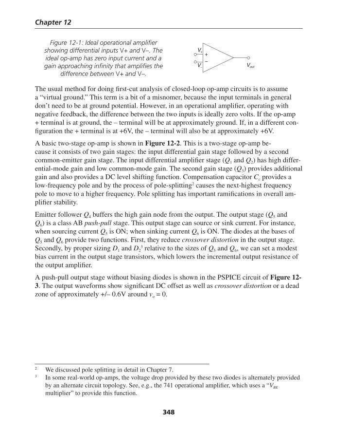
Chapter 12
348
The usual method for doing fi rst-cut analysis of closed-loop op-amp circuits is to assume a “virtual ground.” This term is a bit of a misnomer, because the input terminals in general don’t need to be at ground potential. However, in an operational amplifi er, operating with negative feedback, the difference between the two inputs is ideally zero volts. If the op-amp + terminal is at ground, the – terminal will be at approximately ground. If, in a different con-fi guration the + terminal is at +6V, the – terminal will also be at approximately +6V.
A basic two-stage op-amp is shown in Figure 12-2. This is a two-stage op-amp be-cause it consists of two gain stages: the input differential gain stage followed by a second common-emitter gain stage. The input differential amplifi er stage (Q1 and Q2) has high differ-ential-mode gain and low common-mode gain. The second gain stage (Q3) provides additional gain and also provides a DC level shifting function. Compensation capacitor Cc provides a low-frequency pole and by the process of pole-splitting2 causes the next-highest frequency pole to move to a higher frequency. Pole splitting has important ramifi cations in overall am-plifi er stability.
Emitter follower Q4 buffers the high gain node from the output. The output stage (Q5 and Q6) is a class AB push-pull stage. This output stage can source or sink current. For instance, when sourcing current Q5 is ON; when sinking current Q6 is ON. The diodes at the bases of Q5 and Q6 provide two functions. First, they reduce crossover distortion in the output stage. Secondly, by proper sizing D1 and D2
3 relative to the sizes of Q5 and Q6, we can set a modest bias current in the output stage transistors, which lowers the incremental output resistance of the output amplifi er.
A push-pull output stage without biasing diodes is shown in the PSPICE circuit of Figure 12-3. The output waveforms show signifi cant DC offset as well as crossover distortion or a dead zone of approximately +/– 0.6V around vo = 0.
Vout
V+
V–
+−
Figure 12-1: Ideal operational amplifi er showing differential inputs V+ and V–. The ideal op-amp has zero input current and a gain approaching infi nity that amplifi es the
difference between V+ and V–.
2 We discussed pole splitting in detail in Chapter 7.3 In some real-world op-amps, the voltage drop provided by these two diodes is alternately provided
by an alternate circuit topology. See, e.g., the 741 operational amplifi er, which uses a “VBE multiplier” to provide this function.
Thompson Book.indb 348 3/20/2006 11:36:37 AM
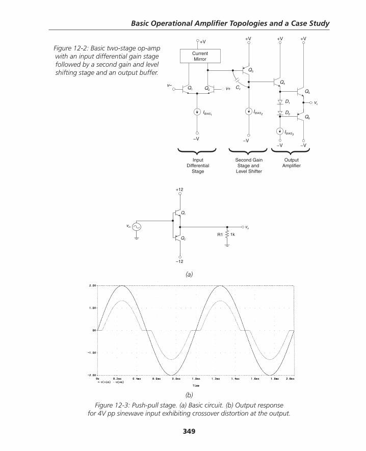
Basic Operational Amplifi er Topologies and a Case Study
349
(b)
Figure 12-3: Push-pull stage. (a) Basic circuit. (b) Output response for 4V pp sinewave input exhibiting crossover distortion at the output.
Q3
InputDifferential
Stage
{Second GainStage and
Level Shifter
{
OutputAmplifier
{
Q4
Q5
Q6
Q2Q1
+V+V +V +V
−V−V−V−V
v−v+ Cc
IBIAS1IBIAS2
IBIAS3
voD1
D2
CurrentMirror
Figure 12-2: Basic two-stage op-amp with an input differential gain stage followed by a second gain and level shifting stage and an output buffer.
+12
1kR1
Q1
vin
−12
Q2
vo
(a)
Thompson Book.indb 349 3/20/2006 11:36:38 AM
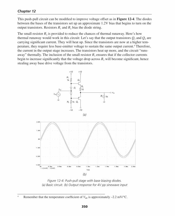
Chapter 12
350
This push-pull circuit can be modifi ed to improve voltage offset as in Figure 12-4. The diodes between the bases of the transistors set up an approximate 1.2V bias that begins to turn on the output transistors. Resistors R1 and R2 bias the diode string.
The small resistor R3 is provided to reduce the chances of thermal runaway. Here’s how thermal runaway would work in this circuit: Let’s say that the output transistors Q3 and Q4 are carrying signifi cant current. They will heat up. Since the transistors are now at a higher tem-perature, they require less base-emitter voltage to sustain the same output current.4 Therefore, the current in the output stage increases. The transistors heat up more, and the circuit “runs-away” thermally. The inclusion of the small resistor R3 ensures that if the collector currents begin to increase signifi cantly that the voltage drop across R3 will become signifi cant, hence stealing away base drive voltage from the transistors.
(a)
4 Remember that the temperature coeffi cient of VBE is approximately –2.2 mV/°C.
vin2
−12 −12
+12+12
D1vin2
R2
R3
Q4
Q31k
R1
1k
vo2
10
RL 1k
(b)
Figure 12-4: Push-pull stage with base biasing diodes. (a) Basic circuit. (b) Output response for 4V pp sinewave input
Thompson Book.indb 350 3/20/2006 11:36:39 AM
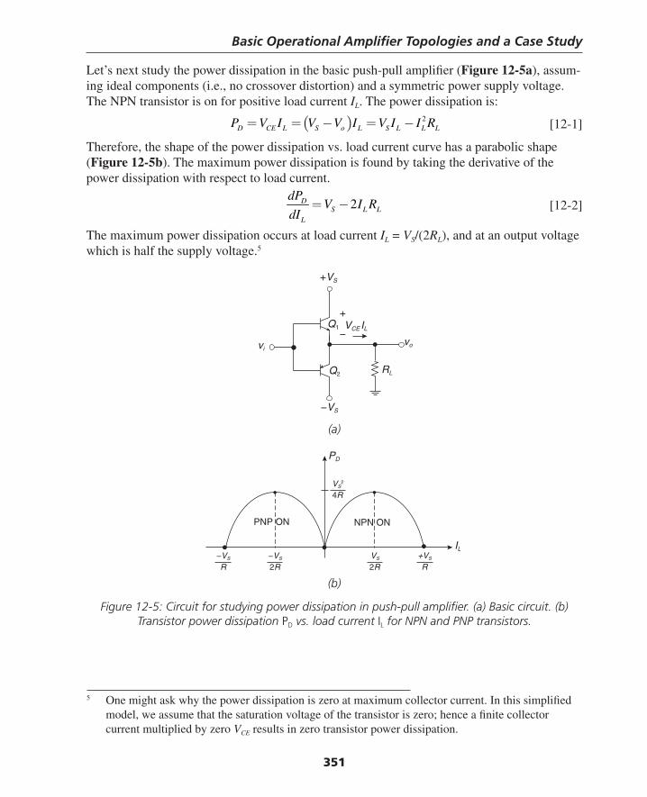
Basic Operational Amplifi er Topologies and a Case Study
351
Let’s next study the power dissipation in the basic push-pull amplifi er (Figure 12-5a), assum-ing ideal components (i.e., no crossover distortion) and a symmetric power supply voltage. The NPN transistor is on for positive load current IL. The power dissipation is:
( ) 2D CE L S o L S L L LP V I V V I V I I R= = − = − [12-1]
Therefore, the shape of the power dissipation vs. load current curve has a parabolic shape (Figure 12-5b). The maximum power dissipation is found by taking the derivative of the power dissipation with respect to load current.
2DS L L
L
dPV I R
dI= − [12-2]
The maximum power dissipation occurs at load current IL = VS/(2RL), and at an output voltage which is half the supply voltage.5
5 One might ask why the power dissipation is zero at maximum collector current. In this simplifi ed model, we assume that the saturation voltage of the transistor is zero; hence a fi nite collector current multiplied by zero VCE results in zero transistor power dissipation.
(a)
vi
Q2 RL
vo
Q1
+VS
−VS
VCE IL
+
−
PD
IL
PNP ON NPN ON
−VS
2R−VS
RVS
2R+VS
R
VS2
4R
(b)
Figure 12-5: Circuit for studying power dissipation in push-pull amplifi er. (a) Basic circuit. (b) Transistor power dissipation PD vs. load current IL for NPN and PNP transistors.
Thompson Book.indb 351 3/20/2006 11:36:40 AM
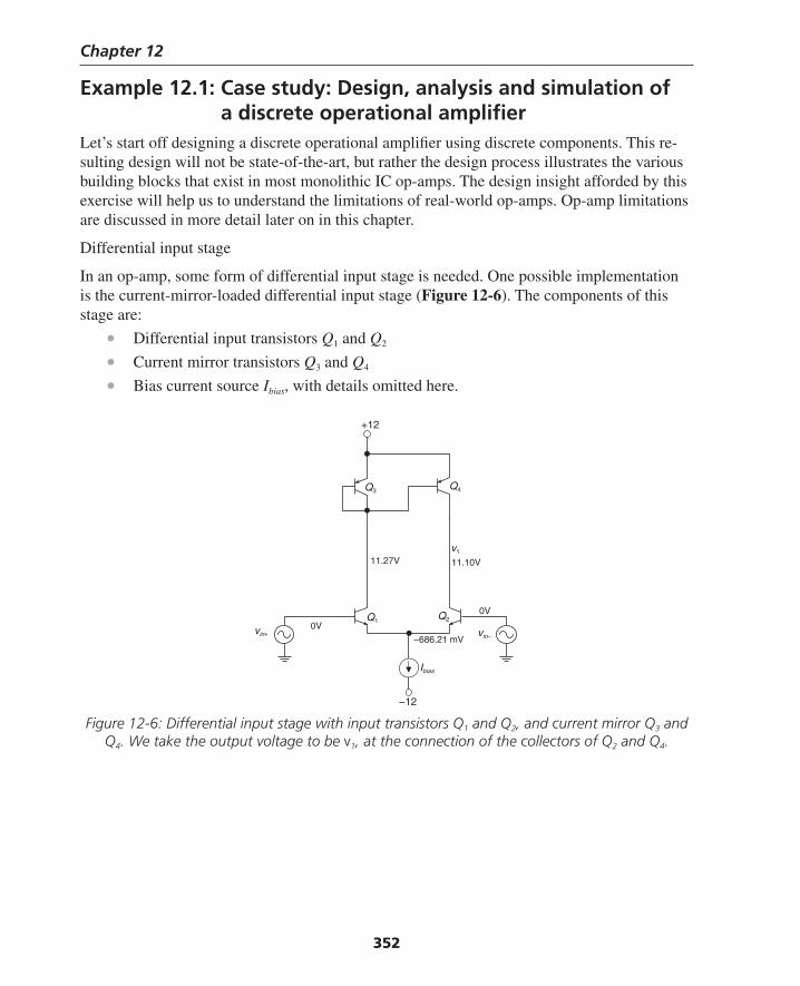
Chapter 12
352
Example 12.1: Case study: Design, analysis and simulation of a discrete operational amplifi erLet’s start off designing a discrete operational amplifi er using discrete components. This re-sulting design will not be state-of-the-art, but rather the design process illustrates the various building blocks that exist in most monolithic IC op-amps. The design insight afforded by this exercise will help us to understand the limitations of real-world op-amps. Op-amp limitations are discussed in more detail later on in this chapter.
Differential input stage
In an op-amp, some form of differential input stage is needed. One possible implementation is the current-mirror-loaded differential input stage (Figure 12-6). The components of this stage are:
• Differential input transistors Q1 and Q2
• Current mirror transistors Q3 and Q4
• Bias current source Ibias, with details omitted here.
vin+
Q2Q1
+12
Q3 Q4
v1
vin−
Ibias
11.10V11.27V
0V
0V
−686.21 mV
−12
Figure 12-6: Differential input stage with input transistors Q1 and Q2, and current mirror Q3 and Q4. We take the output voltage to be v1, at the connection of the collectors of Q2 and Q4.
Thompson Book.indb 352 3/20/2006 11:36:40 AM
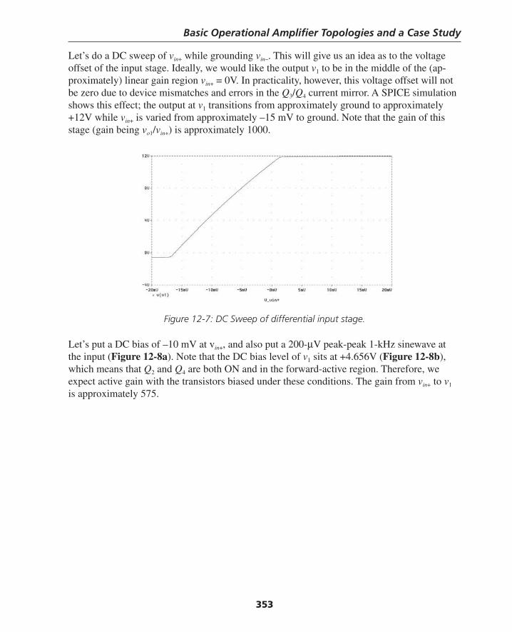
Basic Operational Amplifi er Topologies and a Case Study
353
Let’s do a DC sweep of vin+ while grounding vin–. This will give us an idea as to the voltage offset of the input stage. Ideally, we would like the output v1 to be in the middle of the (ap-proximately) linear gain region vin+ = 0V. In practicality, however, this voltage offset will not be zero due to device mismatches and errors in the Q3/Q4 current mirror. A SPICE simulation shows this effect; the output at v1 transitions from approximately ground to approximately +12V while vin+ is varied from approximately –15 mV to ground. Note that the gain of this stage (gain being vo1/vin+) is approximately 1000.
Figure 12-7: DC Sweep of differential input stage.
Let’s put a DC bias of –10 mV at vin+, and also put a 200-μV peak-peak 1-kHz sinewave at the input (Figure 12-8a). Note that the DC bias level of v1 sits at +4.656V (Figure 12-8b), which means that Q2 and Q4 are both ON and in the forward-active region. Therefore, we expect active gain with the transistors biased under these conditions. The gain from vin+ to v1 is approximately 575.
Thompson Book.indb 353 3/20/2006 11:36:41 AM
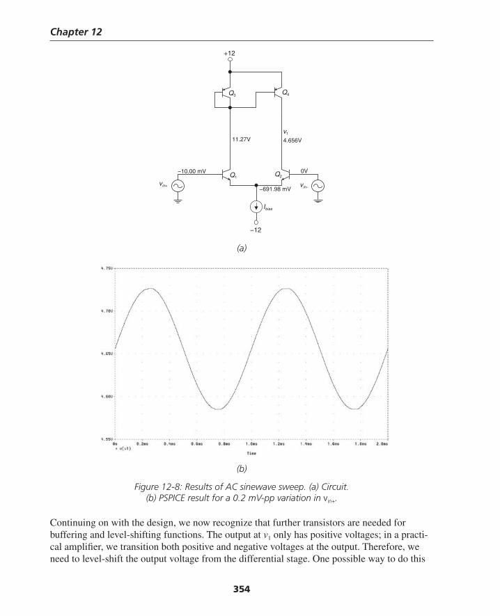
Chapter 12
354
(a)
vin+
Q2Q1
+12
Q3 Q4
v1
vin−
Ibias
4.656V11.27V
−10.00 mV 0V
−691.98 mV
−12
(b)
Figure 12-8: Results of AC sinewave sweep. (a) Circuit. (b) PSPICE result for a 0.2 mV-pp variation in vin+.
Continuing on with the design, we now recognize that further transistors are needed for buffering and level-shifting functions. The output at v1 only has positive voltages; in a practi-cal amplifi er, we transition both positive and negative voltages at the output. Therefore, we need to level-shift the output voltage from the differential stage. One possible way to do this
Thompson Book.indb 354 3/20/2006 11:36:41 AM
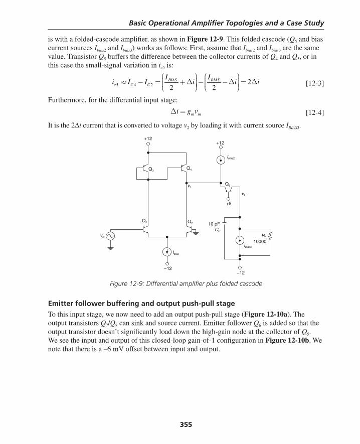
Basic Operational Amplifi er Topologies and a Case Study
355
Q2
Ibias2
Ibias
Q1
Q3Q4
Q5
+12+12
−12−12
Ibias3
v2
v1
vin RL
+6
10 pFCC
10000
is with a folded-cascode amplifi er, as shown in Figure 12-9. This folded cascode (Q5 and bias current sources Ibias2 and Ibias3) works as follows: First, assume that Ibias2 and Ibias3 are the same value. Transistor Q5 buffers the difference between the collector currents of Q4 and Q5, or in this case the small-signal variation in ic5 is:
5 4 2 22 2
BIAS BIASc C C
I Ii I I i i i
⎛ ⎞ ⎛ ⎞⎟ ⎟⎜ ⎜≈ − = + Δ − −Δ = Δ⎟ ⎟⎜ ⎜⎟ ⎟⎟ ⎟⎜ ⎜⎝ ⎠ ⎝ ⎠ [12-3]
Furthermore, for the differential input stage:
m ini g vΔ = [12-4]
It is the 2Δi current that is converted to voltage v2 by loading it with current source IBIAS3.
Figure 12-9: Differential amplifi er plus folded cascode
Emitter follower buffering and output push-pull stageTo this input stage, we now need to add an output push-pull stage (Figure 12-10a). The output transistors Q7/Q8 can sink and source current. Emitter follower Q6 is added so that the output transistor doesn’t signifi cantly load down the high-gain node at the collector of Q5. We see the input and output of this closed-loop gain-of-1 confi guration in Figure 12-10b. We note that there is a –6 mV offset between input and output.
Thompson Book.indb 355 3/20/2006 11:36:42 AM
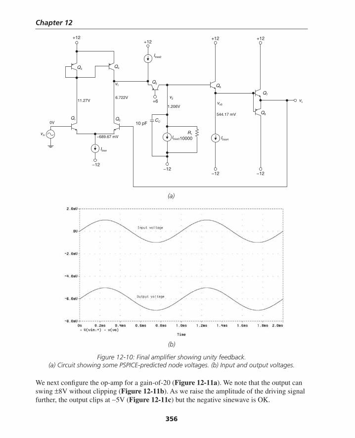
Chapter 12
356
(a)
(b)
Figure 12-10: Final amplifi er showing unity feedback. (a) Circuit showing some PSPICE-predicted node voltages. (b) Input and output voltages.
We next confi gure the op-amp for a gain-of-20 (Figure 12-11a). We note that the output can swing ±8V without clipping (Figure 12-11b). As we raise the amplitude of the driving signal further, the output clips at ∼5V (Figure 12-11c) but the negative sinewave is OK.
Q2
Ibias2
Ibias
Q1
Q3Q4
Q5
+12+12
+12 +12
−12−12
Ibias3
v2
v1
vinR1
+6
10 pF
10000
0V
11.27V
−689.67 mV
6.722V
1.206V
Q6
−12
Ibias4
CC
−12
Q7
vo3
Q8544.17 mV
vo
Thompson Book.indb 356 3/20/2006 11:36:43 AM
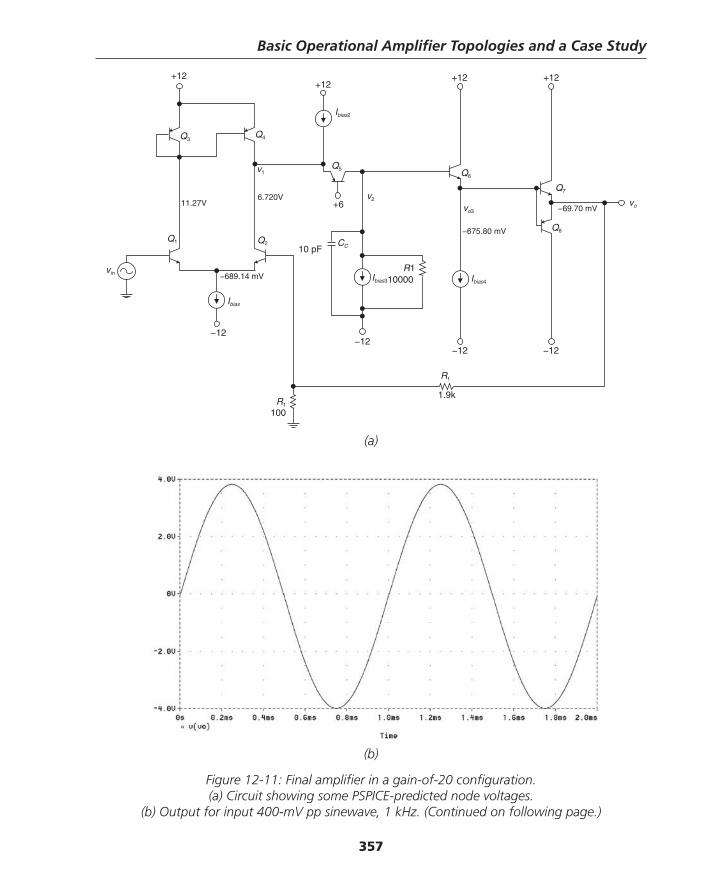
Basic Operational Amplifi er Topologies and a Case Study
357
(a)
Q2
Ibias2
Ibias
Q1
Q3Q4
Q5
+12+12
+12 +12
−12−12
Ibias3
v2
v1
vinR1
+6
10 pF
10000
11.27V
−689.14 mV
6.720V
Q6
−12
Ibias4
CC
−12
−69.70 mV
Q7
vo3
Q8−675.80 mV
vo
R1
100
Rf
1.9k
(b)
Figure 12-11: Final amplifi er in a gain-of-20 confi guration. (a) Circuit showing some PSPICE-predicted node voltages.
(b) Output for input 400-mV pp sinewave, 1 kHz. (Continued on following page.)
Thompson Book.indb 357 3/20/2006 11:36:43 AM
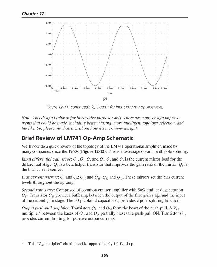
Chapter 12
358
(c)
Figure 12-11 (continued): (c) Output for input 600-mV pp sinewave.
Note: This design is shown for illustrative purposes only. There are many design improve-ments that could be made, including better biasing, more intelligent topology selection, and the like. So, please, no diatribes about how it’s a crummy design!
Brief Review of LM741 Op-Amp SchematicWe’ll now do a quick review of the topology of the LM741 operational amplifi er, made by many companies since the 1960s (Figure 12-12). This is a two-stage op-amp with pole splitting.
Input differential gain stage: Q1, Q2, Q3 and Q4. Q5 and Q6 is the current mirror load for the differential stage. Q7 is a beta helper transistor that improves the gain ratio of the mirror. Q8 is the bias current source.
Bias current mirrors: Q8 and Q9; Q10 and Q11; Q12 and Q13. These mirrors set the bias current levels throughout the op-amp.
Second gain stage: Comprised of common emitter amplifi er with 50Ω emitter degeneration Q17. Transistor Q15 provides buffering between the output of the fi rst gain stage and the input of the second gain stage. The 30-picofarad capacitor C1 provides a pole-splitting function.
Output push-pull amplifi er. Transistors Q14 and Q20 form the heart of the push-pull. A VBE multiplier6 between the bases of Q14 and Q20 partially biases the push-pull ON. Transistor Q15 provides current limiting for positive output currents.
6 This “VBE multiplier” circuit provides approximately 1.6 VBE drop.
Thompson Book.indb 358 3/20/2006 11:36:44 AM
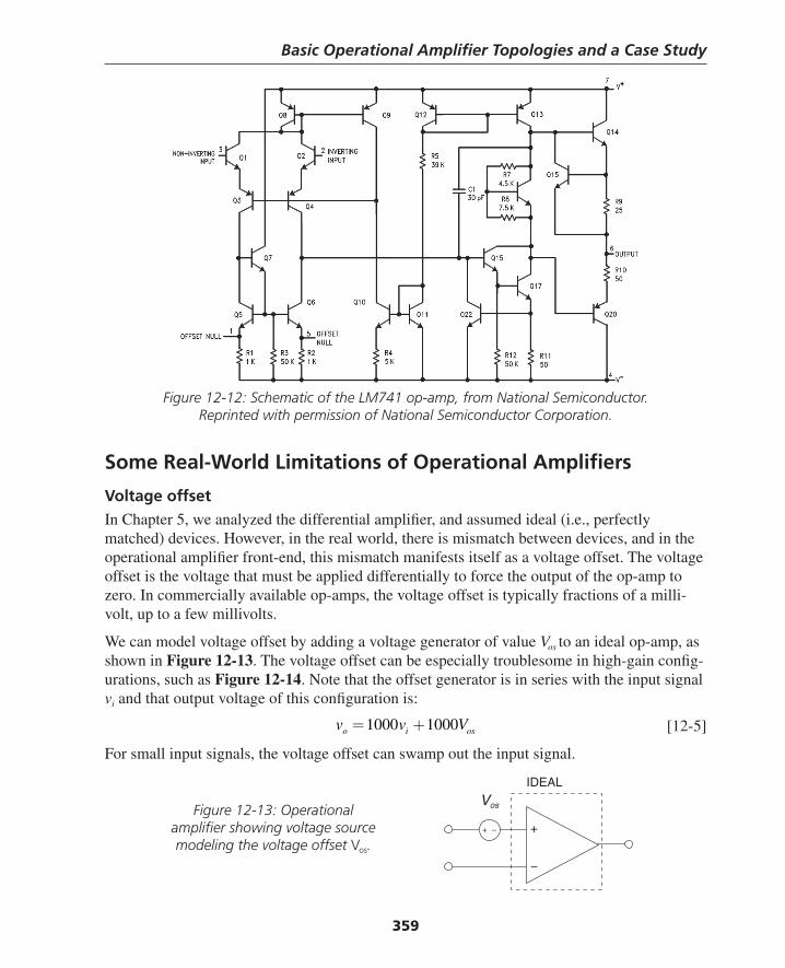
Basic Operational Amplifi er Topologies and a Case Study
359
Figure 12-12: Schematic of the LM741 op-amp, from National Semiconductor.Reprinted with permission of National Semiconductor Corporation.
Some Real-World Limitations of Operational Amplifi ers
Voltage offsetIn Chapter 5, we analyzed the differential amplifi er, and assumed ideal (i.e., perfectly matched) devices. However, in the real world, there is mismatch between devices, and in the operational amplifi er front-end, this mismatch manifests itself as a voltage offset. The voltage offset is the voltage that must be applied differentially to force the output of the op-amp to zero. In commercially available op-amps, the voltage offset is typically fractions of a milli-volt, up to a few millivolts.
We can model voltage offset by adding a voltage generator of value Vos to an ideal op-amp, as shown in Figure 12-13. The voltage offset can be especially troublesome in high-gain confi g-urations, such as Figure 12-14. Note that the offset generator is in series with the input signal vi and that output voltage of this confi guration is:
1000 1000o i osv v V= + [12-5]
For small input signals, the voltage offset can swamp out the input signal.
Figure 12-13: Operational amplifi er showing voltage source modeling the voltage offset Vos.
Vos
IDEAL
+
−
+ −
Thompson Book.indb 359 3/20/2006 11:36:45 AM
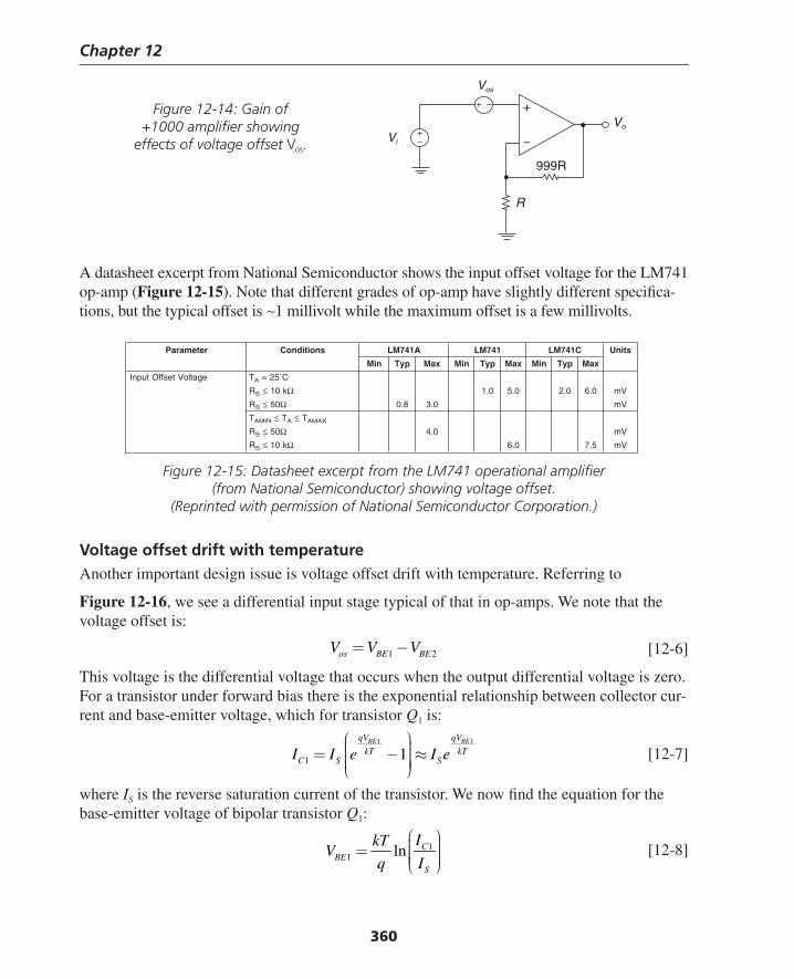
Chapter 12
360
A datasheet excerpt from National Semiconductor shows the input offset voltage for the LM741 op-amp (Figure 12-15). Note that different grades of op-amp have slightly different specifi ca-tions, but the typical offset is ∼1 millivolt while the maximum offset is a few millivolts.
Vos
+
−
+ −
+−
R
Vi
Vo
999R
Figure 12-14: Gain of +1000 amplifi er showing
effects of voltage offset Vos.
Parameter Conditions LM741A LM741 LM741C Units
Min Typ Max Min Typ Max Min Typ Max
Input Offset Voltage TA = 25˚C
RS ≤ 10 kΩ 1.0 5.0 2.0 6.0 mV
RS ≤ 50Ω Vm0.38.0
TAMIN ≤ TA ≤ TAMAX
RS ≤ 50Ω Vm0.4
RS ≤ 10 kΩ 6.0 7.5 mV
Figure 12-15: Datasheet excerpt from the LM741 operational amplifi er (from National Semiconductor) showing voltage offset.
(Reprinted with permission of National Semiconductor Corporation.)
Voltage offset drift with temperatureAnother important design issue is voltage offset drift with temperature. Referring to
Figure 12-16, we see a differential input stage typical of that in op-amps. We note that the voltage offset is:
1 2os BE BEV V V= − [12-6]
This voltage is the differential voltage that occurs when the output differential voltage is zero. For a transistor under forward bias there is the exponential relationship between collector cur-rent and base-emitter voltage, which for transistor Q1 is:
1 1
1 1BE BEqV qV
kT kTC S SI I e I e
⎛ ⎞⎟⎜ ⎟= − ≈⎜ ⎟⎜ ⎟⎟⎜⎝ ⎠ [12-7]
where IS is the reverse saturation current of the transistor. We now fi nd the equation for the base-emitter voltage of bipolar transistor Q1:
11 ln C
BES
IkTV
q I
⎛ ⎞⎟⎜ ⎟= ⎜ ⎟⎜ ⎟⎜⎝ ⎠ [12-8]
Thompson Book.indb 360 3/20/2006 11:36:45 AM
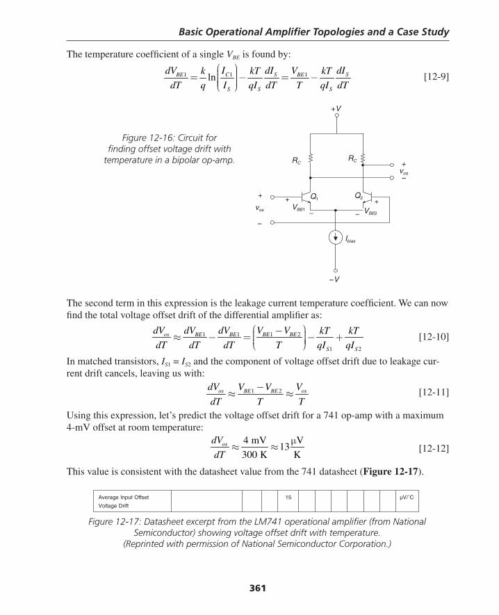
Basic Operational Amplifi er Topologies and a Case Study
361
The temperature coeffi cient of a single VBE is found by:
11 1ln C S SBE BE
S S S
I dI dIdV Vk kT kT
dT q I qI dT T qI dT
⎛ ⎞⎟⎜ ⎟= − = −⎜ ⎟⎜ ⎟⎜⎝ ⎠ [12-9]
The second term in this expression is the leakage current temperature coeffi cient. We can now fi nd the total voltage offset drift of the differential amplifi er as:
1 1 1 2
1 2
os BE BE BE BE
S S
dV dV dV V V kT kT
dT dT dT T qI qI
⎛ ⎞− ⎟⎜≈ − = − +⎟⎜ ⎟⎟⎜⎝ ⎠ [12-10]
In matched transistors, IS1 = IS2 and the component of voltage offset drift due to leakage cur-rent drift cancels, leaving us with:
1 2os osBE BEdV VV V
dT T T
−≈ ≈ [12-11]
Using this expression, let’s predict the voltage offset drift for a 741 op-amp with a maximum 4-mV offset at room temperature:
4 mV V
13300 K K
osdV
dT
μ≈ ≈ [12-12]
This value is consistent with the datasheet value from the 741 datasheet (Figure 12-17).
vos
Q2Q1
Ibias
+vod−
RCRC
+V
−V
VBE1 VBE2
++
– –
+
−
Figure 12-16: Circuit for fi nding offset voltage drift with
temperature in a bipolar op-amp.
Figure 12-17: Datasheet excerpt from the LM741 operational amplifi er (from National Semiconductor) showing voltage offset drift with temperature.
(Reprinted with permission of National Semiconductor Corporation.)
C˚/Vµ51tesffOtupnIegarevA
Voltage Drift
Thompson Book.indb 361 3/20/2006 11:36:46 AM
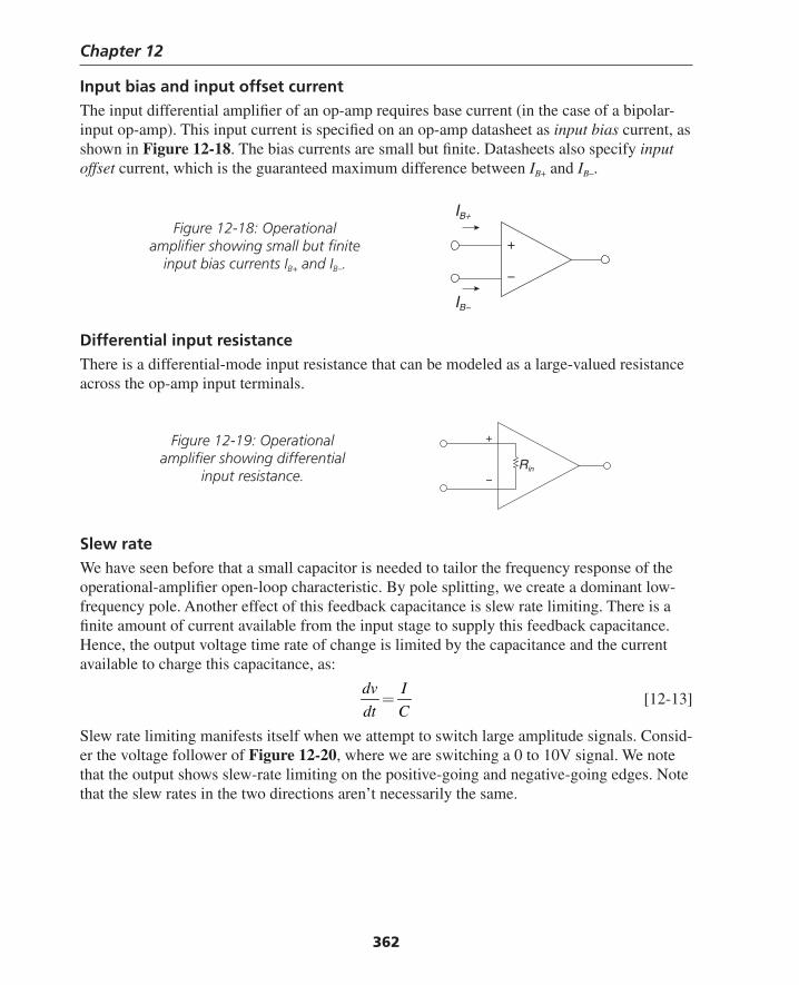
Chapter 12
362
Input bias and input offset currentThe input differential amplifi er of an op-amp requires base current (in the case of a bipolar-input op-amp). This input current is specifi ed on an op-amp datasheet as input bias current, as shown in Figure 12-18. The bias currents are small but fi nite. Datasheets also specify input offset current, which is the guaranteed maximum difference between IB+ and IB–.
Differential input resistanceThere is a differential-mode input resistance that can be modeled as a large-valued resistance across the op-amp input terminals.
IB+
+
−
IB−
Figure 12-18: Operational amplifi er showing small but fi nite
input bias currents IB+ and IB–.
Slew rateWe have seen before that a small capacitor is needed to tailor the frequency response of the operational-amplifi er open-loop characteristic. By pole splitting, we create a dominant low-frequency pole. Another effect of this feedback capacitance is slew rate limiting. There is a fi nite amount of current available from the input stage to supply this feedback capacitance. Hence, the output voltage time rate of change is limited by the capacitance and the current available to charge this capacitance, as:
dv I
dt C= [12-13]
Slew rate limiting manifests itself when we attempt to switch large amplitude signals. Consid-er the voltage follower of Figure 12-20, where we are switching a 0 to 10V signal. We note that the output shows slew-rate limiting on the positive-going and negative-going edges. Note that the slew rates in the two directions aren’t necessarily the same.
+
−Rin
Figure 12-19: Operational amplifi er showing differential
input resistance.
Thompson Book.indb 362 3/20/2006 11:36:47 AM
Basic Operational Amplifi er Topologies and a Case Study
363
(a)
+
−vi(t)
vo+−
10
0
10
0
t
vi(t )
t
vo(t )
odvpos
dtodv
negdt
(b)
Figure 12-20: Circuit that shows effects of slew rate limiting.
Output resistance and capacitive loadingAll operational amplifi ers have a fi nite output resistance. As we’ll see, this fi nite output resis-tance can have a signifi cant effect on closed-loop stability when driving capacitive loads.
Figure 12-21: Operational amplifi er showing output resistance.
IDEAL
Rout
vo
+
−
Example 12.2: Op-amp driving capacitive loadLet’s consider a typical operational amplifi er open-loop transfer function:
( )( )( )
5
7
10
0.01 1 10 1a s
s s−≈
+ + [12-14]
The open-loop transfer function a(s) of this op-amp is plotted in Figure 12-22, where we see the low-frequency pole at 100 radians/second and high-frequency pole at 107 radians/second. This type of transfer function is typical of many commercially available op-amps.
Thompson Book.indb 363 3/20/2006 11:36:48 AM
Chapter 12
364
Figure 12-22: Plot of a(s) for typical op-amp.
We’ll now see what happens if we use this op-amp to drive a capacitive load in a follower confi guration (Figure 12-23a). A model of the op-amp showing the op-amp output resistance is shown in Figure 12-23b. In this example we’ll assume that the output resistance of the op-amp is 100Ω.
Frequency (rad/sec)
Pha
se (
deg)
; Mag
nitu
de (
dB)
Bode Diagrams
−50
0
50
100
100 101 102 103 104 105 106 107 108−200
−150
−100
−50
0
(a) (b)
Figure 12-23: Op-amp follower driving capacitive load. (a) Circuit. (b) Model showing op-amp output resistance ro.
The block diagram of this capacitively loaded amplifi er is shown in Figure 12-24.
v+
v−
a(s)(v+ − v−)
+−
+
−
ro+
−
vovi
CL
+−
vo
Figure 12-24: Capacitively loaded op-amp follower block diagram.
11o Lr C s +
+− a(s)vi vo
Thompson Book.indb 364 3/20/2006 11:36:48 AM
Basic Operational Amplifi er Topologies and a Case Study
365
When we plot the magnitude and phase of the loop transmission (Figure 12-25) we note that there is poor phase margin of 22º. The resultant step response of the closed-loop system (Figure 12-26) shows signifi cant overshoot, as expected, with this low value of phase margin. The low phase margin is due to the low-pass fi lter inside the feedback loop, due to the op-amp output resistance interacting with the load capacitor.
Figure 12-25: Plot of loop transmission gain and phase, showing phase margin of op-amp when loaded with 1000 pF of 21.7º.
Frequency (rad/sec)
Pha
se (
deg)
; Mag
nitu
de (
dB)
Bode DiagramsGm=6.1 dB (Wcg=9975724.1); Pm=21.7 deg. (Wcp=6747944.7)
−100
-50
0
50
100
100 101 102 103 104 105 106 107 108−300
−250
−200
−150
−100
−50
0
Figure 12-26: Unit step response of capacitively loaded follower.Time (sec.)
Am
plitu
de
Step ResponseClosed loop step response, with capacitive load
0 0.5 1 1.5 2 2.5 3 3.5 4 4.5 5
x 10−6
0
0.2
0.4
0.6
0.8
1
1.2
1.4
1.6
Thompson Book.indb 365 3/20/2006 11:36:49 AM
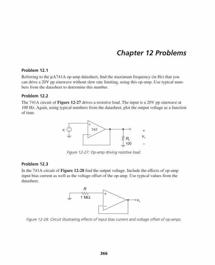
366
Chapter 12 Problems
Problem 12.1Referring to the μA741A op-amp datasheet, fi nd the maximum frequency (in Hz) that you can drive a 20V pp sinewave without slew rate limiting, using this op-amp. Use typical num-bers from the datasheet to determine this number.
Problem 12.2The 741A circuit of Figure 12-27 drives a resistive load. The input is a 20V pp sinewave at 100 Hz. Again, using typical numbers from the datasheet, plot the output voltage as a function of time
Figure 12-27: Op-amp driving resistive load.
Problem 12.3In the 741A circuit of Figure 12-28 fi nd the output voltage. Include the effects of op-amp input bias current as well as the voltage offset of the op-amp. Use typical values from the datasheet.
+
−
vo
vi
RL
100
+− 741
+
−
Figure 12-28: Circuit illustrating effects of input bias current and voltage offset of op-amps.
+
−
vo
R
1 MΩ
Thompson Book.indb 366 3/20/2006 11:36:49 AM
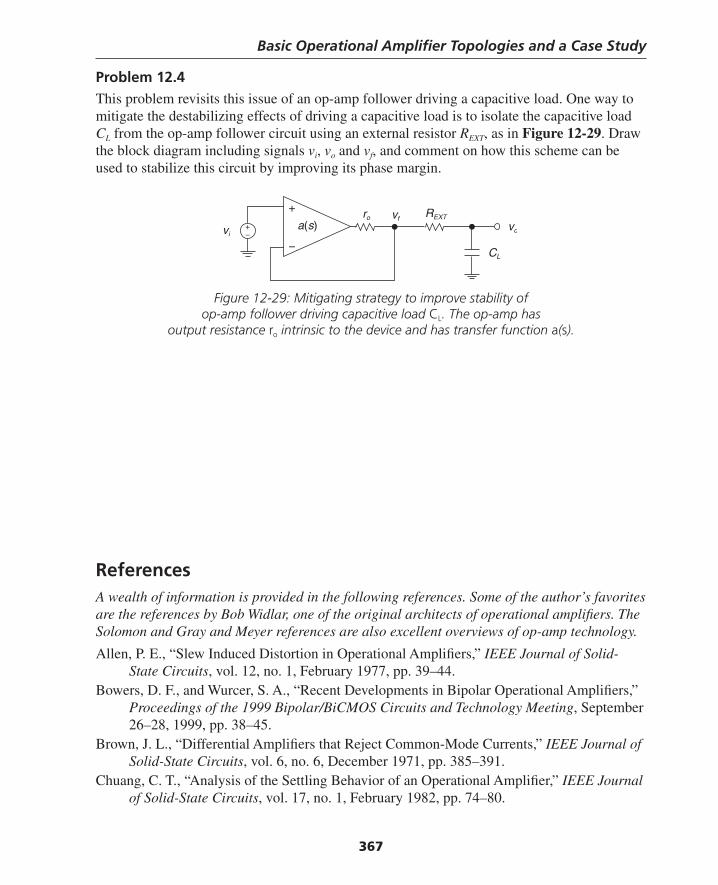
Basic Operational Amplifi er Topologies and a Case Study
367
Problem 12.4This problem revisits this issue of an op-amp follower driving a capacitive load. One way to mitigate the destabilizing effects of driving a capacitive load is to isolate the capacitive load CL from the op-amp follower circuit using an external resistor REXT, as in Figure 12-29. Draw the block diagram including signals vi, vo and vf, and comment on how this scheme can be used to stabilize this circuit by improving its phase margin.
Figure 12-29: Mitigating strategy to improve stability ofop-amp follower driving capacitive load CL. The op-amp has
output resistance ro intrinsic to the device and has transfer function a(s).
vf REXT
vovi
CL
ro+−
+
−
a(s)
ReferencesA wealth of information is provided in the following references. Some of the author’s favorites are the references by Bob Widlar, one of the original architects of operational amplifi ers. The Solomon and Gray and Meyer references are also excellent overviews of op-amp technology.
Allen, P. E., “Slew Induced Distortion in Operational Amplifi ers,” IEEE Journal of Solid-State Circuits, vol. 12, no. 1, February 1977, pp. 39–44.
Bowers, D. F., and Wurcer, S. A., “Recent Developments in Bipolar Operational Amplifi ers,” Proceedings of the 1999 Bipolar/BiCMOS Circuits and Technology Meeting, September 26–28, 1999, pp. 38–45.
Brown, J. L., “Differential Amplifi ers that Reject Common-Mode Currents,” IEEE Journal of Solid-State Circuits, vol. 6, no. 6, December 1971, pp. 385–391.
Chuang, C. T., “Analysis of the Settling Behavior of an Operational Amplifi er,” IEEE Journal of Solid-State Circuits, vol. 17, no. 1, February 1982, pp. 74–80.
Thompson Book.indb 367 3/20/2006 11:36:50 AM
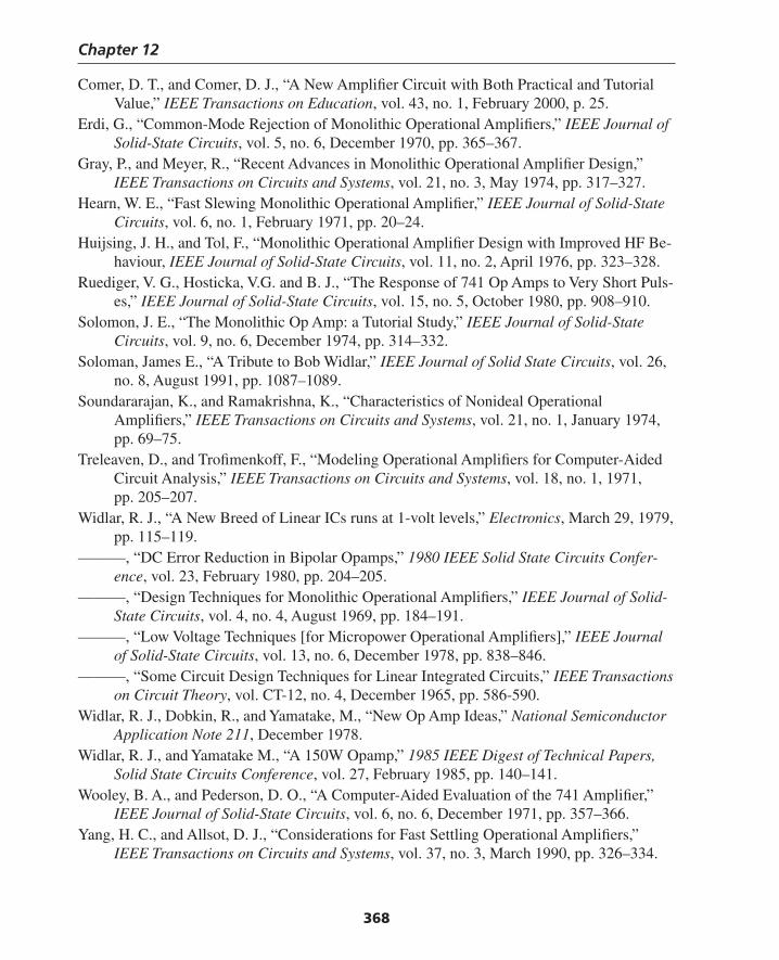
Chapter 12
368
Comer, D. T., and Comer, D. J., “A New Amplifi er Circuit with Both Practical and Tutorial Value,” IEEE Transactions on Education, vol. 43, no. 1, February 2000, p. 25.
Erdi, G., “Common-Mode Rejection of Monolithic Operational Amplifi ers,” IEEE Journal of Solid-State Circuits, vol. 5, no. 6, December 1970, pp. 365–367.
Gray, P., and Meyer, R., “Recent Advances in Monolithic Operational Amplifi er Design,” IEEE Transactions on Circuits and Systems, vol. 21, no. 3, May 1974, pp. 317–327.
Hearn, W. E., “Fast Slewing Monolithic Operational Amplifi er,” IEEE Journal of Solid-State Circuits, vol. 6, no. 1, February 1971, pp. 20–24.
Huijsing, J. H., and Tol, F., “Monolithic Operational Amplifi er Design with Improved HF Be-haviour, IEEE Journal of Solid-State Circuits, vol. 11, no. 2, April 1976, pp. 323–328.
Ruediger, V. G., Hosticka, V.G. and B. J., “The Response of 741 Op Amps to Very Short Puls-es,” IEEE Journal of Solid-State Circuits, vol. 15, no. 5, October 1980, pp. 908–910.
Solomon, J. E., “The Monolithic Op Amp: a Tutorial Study,” IEEE Journal of Solid-State Circuits, vol. 9, no. 6, December 1974, pp. 314–332.
Soloman, James E., “A Tribute to Bob Widlar,” IEEE Journal of Solid State Circuits, vol. 26, no. 8, August 1991, pp. 1087–1089.
Soundararajan, K., and Ramakrishna, K., “Characteristics of Nonideal Operational Amplifi ers,” IEEE Transactions on Circuits and Systems, vol. 21, no. 1, January 1974, pp. 69–75.
Treleaven, D., and Trofi menkoff, F., “Modeling Operational Amplifi ers for Computer-Aided Circuit Analysis,” IEEE Transactions on Circuits and Systems, vol. 18, no. 1, 1971, pp. 205–207.
Widlar, R. J., “A New Breed of Linear ICs runs at 1-volt levels,” Electronics, March 29, 1979, pp. 115–119.
———, “DC Error Reduction in Bipolar Opamps,” 1980 IEEE Solid State Circuits Confer-ence, vol. 23, February 1980, pp. 204–205.
———, “Design Techniques for Monolithic Operational Amplifi ers,” IEEE Journal of Solid-State Circuits, vol. 4, no. 4, August 1969, pp. 184–191.
———, “Low Voltage Techniques [for Micropower Operational Amplifi ers],” IEEE Journal of Solid-State Circuits, vol. 13, no. 6, December 1978, pp. 838–846.
———, “Some Circuit Design Techniques for Linear Integrated Circuits,” IEEE Transactions on Circuit Theory, vol. CT-12, no. 4, December 1965, pp. 586-590.
Widlar, R. J., Dobkin, R., and Yamatake, M., “New Op Amp Ideas,” National Semiconductor Application Note 211, December 1978.
Widlar, R. J., and Yamatake M., “A 150W Opamp,” 1985 IEEE Digest of Technical Papers, Solid State Circuits Conference, vol. 27, February 1985, pp. 140–141.
Wooley, B. A., and Pederson, D. O., “A Computer-Aided Evaluation of the 741 Amplifi er,” IEEE Journal of Solid-State Circuits, vol. 6, no. 6, December 1971, pp. 357–366.
Yang, H. C., and Allsot, D. J., “Considerations for Fast Settling Operational Amplifi ers,” IEEE Transactions on Circuits and Systems, vol. 37, no. 3, March 1990, pp. 326–334.
Thompson Book.indb 368 3/20/2006 11:36:50 AM
369
C H A P T E R 13Review of Current Feedback
Operational Amplifi ers
Conventional Voltage-Feedback Op-Amp and the Constant “Gain Bandwidth Product” ParadigmA conventional voltage-feedback operational amplifi er is shown in Figure 13-1. Let’s assume that the op-amp is dominated by a single pole at a very low frequency. We can express the op-amp open-loop transfer function under this assumption as:1
( )1
oA Ka s
s sτ≈ ≈
+ [13-1]
where Ao is the DC gain of the amplifi er and 1/τ is the pole frequency of the op-amp dominant pole. Note that we’re approximating the op-amp as behaving as an integrator for frequencies of interest. This simplifi es the mathematics in the following discussion considerably.
In This Chapter
Current-feedback operational amplifi ers are devices where the main feedback path from output to input carries a current, and not a voltage, as in voltage feedback op-amps. Current-feedback op-amps do not suffer from the gain bandwidth product paradigm as do voltage feedback operational amplifi ers, and can achieve very high bandwidths. However, they do have other limitations.
1 Since we’re interested in the detail of the high-frequency breakpoint, we’ll make the simplifying assumption that the low-frequency pole is at or near DC. This simplifi es the math signifi cantly. In a generic op-amp there’s a dominant pole at a very low frequency and higher-frequency poles that can affect closed-loop stability. The dominant pole is at approximately gm/Cc, where gm is the transconductance of the input stage and Cc is the compensating capacitor value. For typical op-amps, this dominant pole is at a few hertz.
Thompson Book.indb 369 3/20/2006 11:36:50 AM
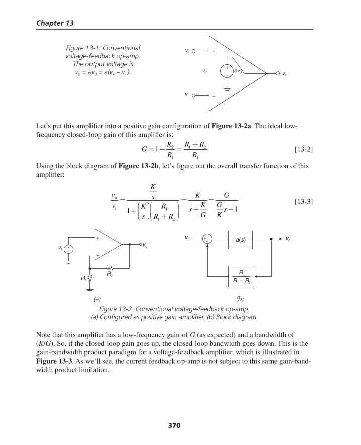
Chapter 13
370
Let’s put this amplifi er into a positive gain confi guration of Figure 13-2a. The ideal low- frequency closed-loop gain of this amplifi er is:
2 1 2
1 1
1R R R
GR R
+= + = [13-2]
Using the block diagram of Figure 13-2b, let’s fi gure out the overall transfer function of this amplifi er:
1
1 2
11
o
i
Kv K Gs
K Gv RK s sG Ks R R
= = =⎛ ⎞⎛ ⎞ ⎟⎜⎟ + +⎜ ⎟+ ⎜⎟⎜ ⎟⎟⎜⎜ ⎟⎜⎝ ⎠ +⎝ ⎠
[13-3]
vo
v+ +
−v−
vd avd
++−
Figure 13-1: Conventional voltage-feedback op-amp.
The output voltage isvo = avd = a(v+ – v– ).
(a) (b)
Figure 13-2: Conventional voltage-feedback op-amp. (a) Confi gured as positive gain amplifi er. (b) Block diagram.
Note that this amplifi er has a low-frequency gain of G (as expected) and a bandwidth of (K/G). So, if the closed-loop gain goes up, the closed-loop bandwidth goes down. This is the gain-bandwidth product paradigm for a voltage-feedback amplifi er, which is illustrated in Figure 13-3. As we’ll see, the current feedback op-amp is not subject to this same gain-band-width product limitation.
vo
+
−vi
R1
R2
vovi
+−
+−
1
1 2
RR R+
a(s)
Thompson Book.indb 370 3/20/2006 11:36:51 AM
Review of Current Feedback Operational Amplifi ers
371
Slew Rate Limitations in Conventional Op-AmpsIn a conventional operational amplifi er, a compensating capacitor is used to tailor the open-loop frequency response so that it is dominated by a single pole. In a conventional internally compensated op-amp (such as the LM741 in Figure 13-3 below) there is a compensating capacitor internal to the device. The maximum rate at which we can charge and discharge this capacitor (and hence the output voltage) depends on the bias current for the previous differential stage (provided originally by Q8). The specifi cation for slew rate for this op-amp is ∼0.5 μs, consistent with an input bias current of ∼15 μA.2
GAIN
A = 100
A = 1
A = 10
ff100 f10 f1
01277525
Figure 13-3: Illustration of gain-bandwidth product for conventional voltage-feedback
amplifi er. As the closed-loop gain is increased, the closed-loop bandwidth decreases.
2 The slew rate calculation is simple enough: dV/dt = I/C where I is the input stage bias current and C is the compensation capacitor value. A detailed look at the inner workings of the LM741 can be found in Gray, Hurst Lewis and Meyer, Analysis and Design of Analog Integrated Circuits, 4th edition, Chapter 6.8. It is shown in this reference that I ~ 19 μA which results in a slew rate of ~0.6 V/μsec for a 30-pF compensating capacitor.
3 This particular datasheet is from National Semiconductor; other vendors make this op-amp as well.Reprinted with permission of National Semiconductor.
Figure 13-4: LM741 simplifi ed schematic.3 Note the 30-pF compensation capacitor C1.
Thompson Book.indb 371 3/20/2006 11:36:52 AM
Chapter 13
372
Basic Current Feedback Op-AmpThe basic current-feedback op-amp (Figure 13-5) differs from the conventional voltage-feed-back op-amp in several respects. The negative input (v–) has a very low input impedance (by design), since this negative node is the place where we’ll be feeding back current. A unity-gain buffer (Q1–Q3 and Q2–Q4) forces the v– input to follow the v+ input.4
Since we use negative current feedback to the inverting v– input,5 we want low output impedance at this v– node, so that the input impedance won’t signifi cantly affect the amount of current that is fed back. The input amplifi er Q3/Q4 and associated current mirrors convert the feedback current if fl owing out of the negative input to a voltage at the high-gain node at the output of the current mirrors. This voltage at the high-gain node is further buffered by a unity-gain buffer to the output.
4 This type of 4-transistor follower is sometimes called a “diamond buffer” or a “diamond follower.” See, e.g., Burr-Brown (later, Texas Instruments) application note AB-181 by K. Lehmann, “Diamond Transistor OPA660,” and W. Lillis and A. Wang, “Complementary current mirror for correcting input offset voltage of diamond follower, especially as input stage for wideband amplifi er,” U.S. Patent # 4,893,091, issued January 9, 1990.
5 The concept of current feedback is not new; designs for tube amplifi ers using cathode feedback date back to the 1920s.
Figure 13-5: One topology of the current-feedback opamp.
Mirror
Mirror
−v
+v
vo+1
C
v −
+v
IB1
IB2
ifQ4
Q3
Q1
Q2
+v
−v
v +
−v
Note that in Figure 13-5 no voltage amplifi cation occurs inside the amplifi er. The input fol-lowers Q1–Q2–Q3–Q4 have a voltage gain of +1. The current mirrors provide a current gain of +1 with very little voltage gain. At the high-gain node the mirror current is converted to a voltage, which is buffered to the output. Therefore, there is no “Miller effect” in the current-feedback amplifi er.
Thompson Book.indb 372 3/20/2006 11:36:52 AM
Review of Current Feedback Operational Amplifi ers
373
In order to analyze approximately the gain and bandwidth of the current-feedback op-amp, let’s consider a simplifi ed model that captures the fi rst-order effects. Figure 13-6 shows this current-feedback op-amp reduced to a simplifi ed form. The input resistance Rin is the parallel combination of the output resistances of Q3 and Q4:6
3 4
1 1in
m m
Rg g
≈ [13-4]
For a Q3/Q4 bias current of 250 microamps, this input resistance is approximately 52Ω.7
To fi rst-order, this amplifi er has a single pole due to the RTCT time constant of the high-gain node. The resistance RT at the high-gain node is a combination of the output resistances of the high-side and low-side current mirrors. Assuming that we have cascoded or Wilson current mirrors (to increase the output resistance) the resistance at the high-gain node is:
, ,
2 2npn npn
T
r rR μ μ≈ [13-5]
Assuming a 250-µA mirror bias current and base-width modulation factors ηnpn = ηpnp = 10–3, and with βFnpn = βFpnp = 100, this high-gain node resistance RT = 2.6 MΩ.8
The capacitor CT is set by device parameter and layout parasitics.
6 This simplifi ed calculation ignores the base-spreading resistance rx.7 Remember that the input resistance looking into the emitter of a transistor in the forward active
region is approximately 1/gm, if the base resistance rx and the source resistance seen from the base terminal are neglected. The input resistance, in close form, is:
,
1,
1s x
in emitter s xfe m
R r rr if R r r
h gπ
π
+ +≈ ≈
+8 These numbers are consistent with the Analog Devices AD844, which lists a nominal input
resistance at the inverting input of 50Ω, and a high-gain node resistance of 3 MΩ.
Figure 13-6: Equivalent diagram of current-feedback op-amp.The feedback current if is mirrored to the high gain node.
If we’re interested in DC accuracy, the DC voltage gain of this amplifi er is of importance. The open loop voltage gain is:
6
,
2.6 1050,000
52T
v olin
Ra
R
×≈ ≈ ≈ [13-6]
vo
Rin if CT RT
ifv+
v −
+1+1
Thompson Book.indb 373 3/20/2006 11:36:53 AM
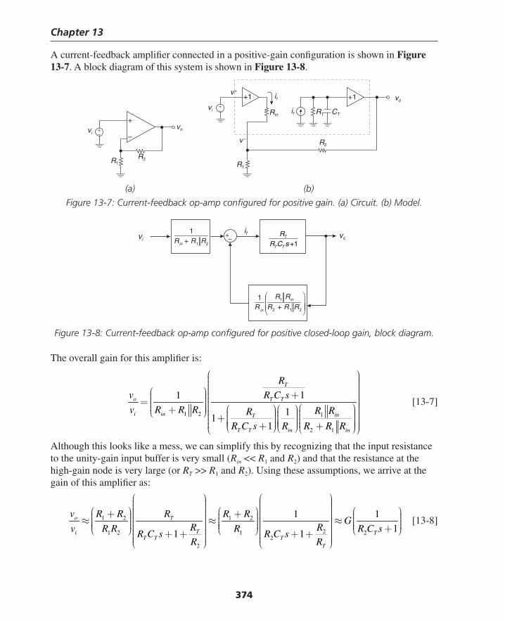
Chapter 13
374
A current-feedback amplifi er connected in a positive-gain confi guration is shown in Figure 13-7. A block diagram of this system is shown in Figure 13-8.
(a) (b)
Figure 13-7: Current-feedback op-amp confi gured for positive gain. (a) Circuit. (b) Model.
vo
R1
CTRTif
v+
v −
+
−
R2
R1
R2
vi
vi Rin
if
+−
+−
+1 +1 vo
Figure 13-8: Current-feedback op-amp confi gured for positive closed-loop gain, block diagram.
The overall gain for this amplifi er is:
1 2 1
2 1
11
11
1
T
o T T
i in inT
T T in in
R
v R C s
v R R R R RR
R C s R R R R
⎛ ⎞⎟⎜ ⎟⎜ ⎟⎜ ⎟⎛ ⎞⎜ ⎟+⎟⎜⎜ ⎟⎟⎜⎜ ⎟= ⎟ ⎟⎜⎜ ⎟ ⎛ ⎞⎟⎛ ⎞⎛ ⎞⎟⎜ ⎜+⎝ ⎠ ⎟⎟⎜⎜ ⎟⎟⎜⎜ ⎟⎟⎟⎟ ⎜⎜ + ⎜⎜ ⎟⎟⎟⎟ ⎜⎜ ⎜⎜ ⎟⎟⎟ ⎟⎜ ⎜ ⎟⎜+ + ⎟⎜ ⎝ ⎠⎝ ⎠⎝ ⎠⎝ ⎠
[13-7]
Although this looks like a mess, we can simplify this by recognizing that the input resistance to the unity-gain input buffer is very small (Rin << R1 and R2) and that the resistance at the high-gain node is very large (or RT >> R1 and R2). Using these assumptions, we arrive at the gain of this amplifi er as:
1 2 1 2
21 2 1 22
2
1 1
11 1
o T
Ti TT T T
T
v R R R R RG
R Rv R R R R C sR C s R C sR R
⎛ ⎞ ⎛ ⎞⎟ ⎟⎜ ⎜⎟ ⎟⎜ ⎜⎟ ⎟⎛ ⎞ ⎛ ⎞ ⎛ ⎞⎜ ⎜+ +⎟ ⎟⎟ ⎟ ⎟⎜ ⎜⎜ ⎜ ⎜⎟ ⎟⎟ ⎟ ⎟≈ ≈ ≈⎜ ⎜⎜ ⎜ ⎜⎟ ⎟⎟ ⎟ ⎟⎜ ⎜⎟ ⎟⎜ ⎜ ⎜⎟ ⎟ ⎟⎜ ⎜ ⎜ +⎟ ⎟⎜ ⎜⎝ ⎠ ⎝ ⎠ ⎝ ⎠⎟ ⎟⎜ ⎜+ + + +⎟ ⎟⎜ ⎜⎟ ⎟⎜ ⎜⎝ ⎠ ⎝ ⎠
[13-8]
vi
if vo+−
1 2
1
inR R R+ 1T
T T
RR C s +
11 in
in
R R
R 1 22R R R+
Thompson Book.indb 374 3/20/2006 11:36:53 AM
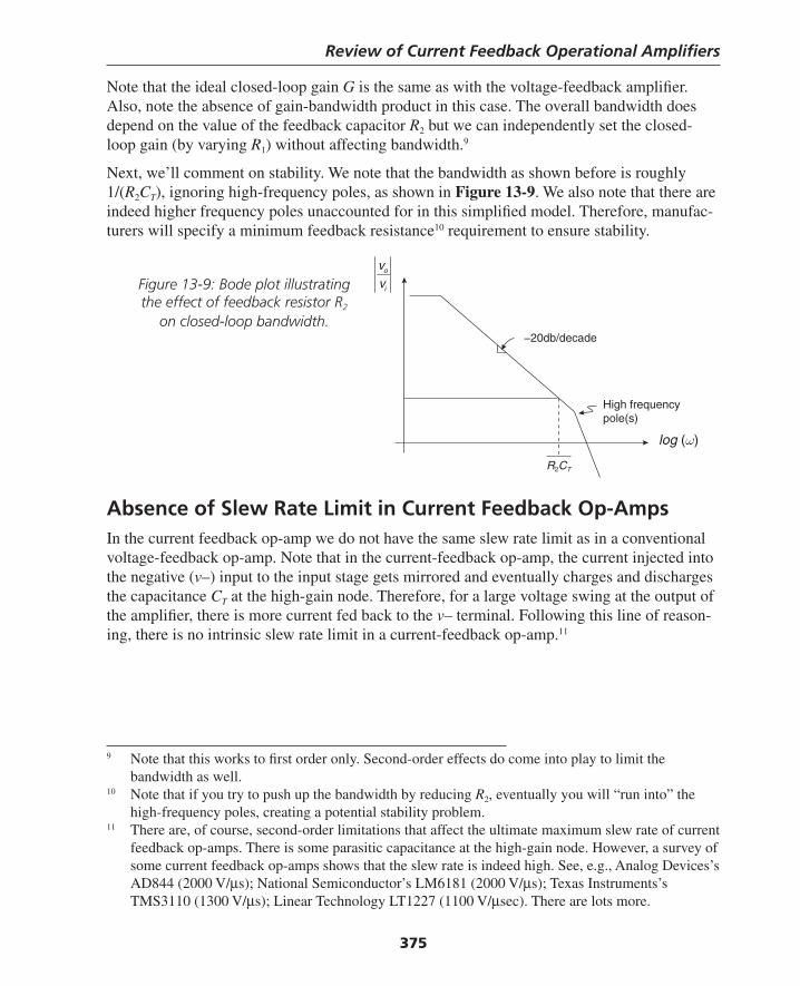
Review of Current Feedback Operational Amplifi ers
375
Note that the ideal closed-loop gain G is the same as with the voltage-feedback amplifi er. Also, note the absence of gain-bandwidth product in this case. The overall bandwidth does depend on the value of the feedback capacitor R2 but we can independently set the closed-loop gain (by varying R1) without affecting bandwidth.9
Next, we’ll comment on stability. We note that the bandwidth as shown before is roughly 1/(R2CT), ignoring high-frequency poles, as shown in Figure 13-9. We also note that there are indeed higher frequency poles unaccounted for in this simplifi ed model. Therefore, manufac-turers will specify a minimum feedback resistance10 requirement to ensure stability.
9 Note that this works to fi rst order only. Second-order effects do come into play to limit the bandwidth as well.
10 Note that if you try to push up the bandwidth by reducing R2, eventually you will “run into” the high-frequency poles, creating a potential stability problem.
11 There are, of course, second-order limitations that affect the ultimate maximum slew rate of current feedback op-amps. There is some parasitic capacitance at the high-gain node. However, a survey of some current feedback op-amps shows that the slew rate is indeed high. See, e.g., Analog Devices’s AD844 (2000 V/μs); National Semiconductor’s LM6181 (2000 V/μs); Texas Instruments’s TMS3110 (1300 V/μs); Linear Technology LT1227 (1100 V/μsec). There are lots more.
Absence of Slew Rate Limit in Current Feedback Op-AmpsIn the current feedback op-amp we do not have the same slew rate limit as in a conventional voltage-feedback op-amp. Note that in the current-feedback op-amp, the current injected into the negative (v–) input to the input stage gets mirrored and eventually charges and discharges the capacitance CT at the high-gain node. Therefore, for a large voltage swing at the output of the amplifi er, there is more current fed back to the v– terminal. Following this line of reason-ing, there is no intrinsic slew rate limit in a current-feedback op-amp.11
o
i
v
v
log (ω)
High frequencypole(s)
R2CT
−20db/decade
Figure 13-9: Bode plot illustrating the effect of feedback resistor R2
on closed-loop bandwidth.
Thompson Book.indb 375 3/20/2006 11:36:54 AM

Chapter 13
376
Example 13.1: An admittedly very crude current-feedback op-amp discrete design Let’s look at an illustrative design of a discrete current-feedback op-amp circuit and simulate with 2N3904 and 2N3906 transistors. Note that this is by no means an optimized design; the resultant design is likely to have problems with voltage offset, transient response and the like. Rather, this simple example illustrates many of the concepts that we’ve gone over in the previous analytic discussion.
Shown in Figure 13-10 is the design, confi gured initially for unity feedback. At fi rst, assume that the value for R1 is 1 MΩ. In this confi guration, we expect approximately unity gain, since, as we’ve shown earlier, the closed-loop gain (at low frequencies) is approximately:
2 1 2
1 1
1R R R
GR R
+= + = [13-9]
Going through the design, we see the following functional blocks:
• Q1–Q4 is the input buffer, providing high input impedance at v+ (the bases of Q1 and Q3) and a low input impedance at v– (the emitters of Q2 and Q4). Q1 and Q3 are biased by current sources, and the collector currents of Q2 and Q4 are approximately:
2 4 1 3C C C CI I I I≈ ≈ [13-10]
We’ll see in a later section in this book (on the translinear principle) how this calculation is done.
• Q5/Q7 and Q6/Q8 are current mirrors that mirror the collector currents of Q2 and Q4 to the high gain node. These mirrors act as a current buffer, mirroring the feedback current to the high gain node. The high gain node is the collector connection of Q7 and Q8. The output resistance at this node is the parallel combination of the output resistances of current mirror transistors Q7 and Q8; the total resistance at this node to ground is this current mirror resistance in parallel with the input resistance of the fol-lower stage Q9 /Q10.
• Q9/Q10 is a unity-gain push-pull output stage, which provides a low impedance at the output vout node.
• R2 is the feedback resistor, and R1 is the input resistor at the inverting input v–. Note that our previous analysis of current-feedback op-amps showed that the main band-width limitation is our selection of feedback resistor R2.
The SPICE bias point values show some interesting results. For instance, the input buf-fer (Q1–Q4) does have a voltage offset as confi gured; note that while the input is at 0V, the negative input (v–) is at –12.9 mV. This voltage offset cascades down through the rest of the amplifi er, resulting in an output voltage of –681 mV when the v+ input is at zero potential.
Thompson Book.indb 376 3/20/2006 11:36:54 AM
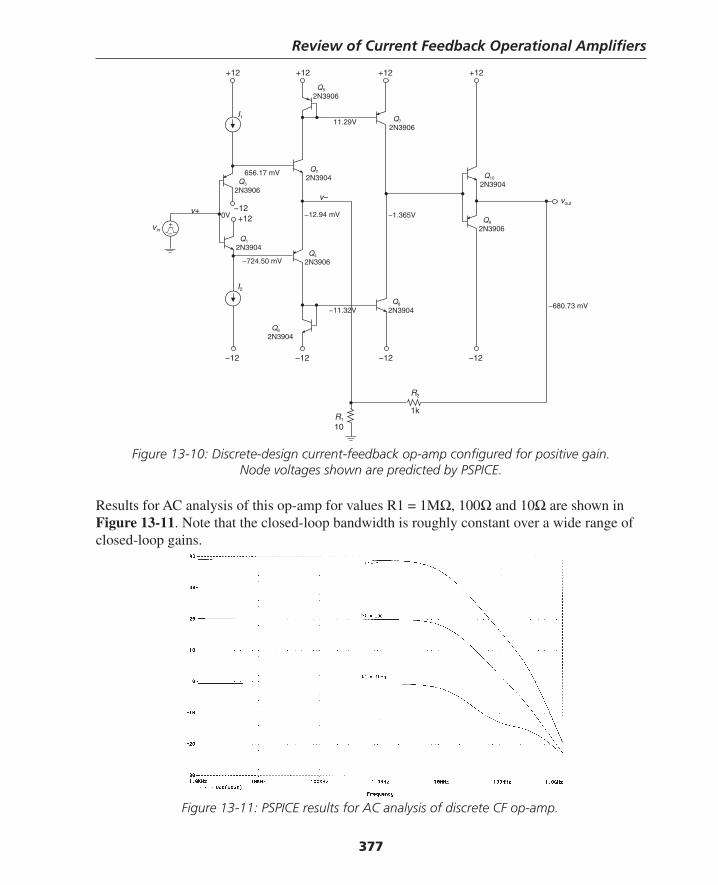
Review of Current Feedback Operational Amplifi ers
377
Figure 13-10: Discrete-design current-feedback op-amp confi gured for positive gain.Node voltages shown are predicted by PSPICE.
Results for AC analysis of this op-amp for values R1 = 1MΩ, 100Ω and 10Ω are shown in Figure 13-11. Note that the closed-loop bandwidth is roughly constant over a wide range of closed-loop gains.
+12 +12 +12 +12
R1
10
−1.365V−12.94 mV
−724.50 mV
+12−12
v−
Q5
2N3906
Q2
2N3904
11.29V
656.17 mV
Q7
2N3906
Q3
2N3906
Q10
2N3904
Q9
2N3906
Q4
2N3906
Q1
2N3904
v+
vin
I2
Q6
2N3904
Q8
2N3904−11.32V
−12 −12 −12 −12
0V
I1
R2
1k
vout
−680.73 mV
+–
Figure 13-11: PSPICE results for AC analysis of discrete CF op-amp.
Thompson Book.indb 377 3/20/2006 11:36:55 AM
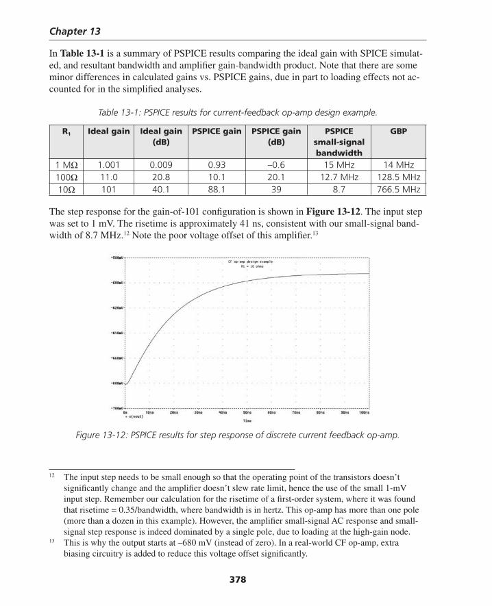
Chapter 13
378
In Table 13-1 is a summary of PSPICE results comparing the ideal gain with SPICE simulat-ed, and resultant bandwidth and amplifi er gain-bandwidth product. Note that there are some minor differences in calculated gains vs. PSPICE gains, due in part to loading effects not ac-counted for in the simplifi ed analyses.
Table 13-1: PSPICE results for current-feedback op-amp design example.
R1 Ideal gain Ideal gain (dB)
PSPICE gain PSPICE gain (dB)
PSPICE small-signal bandwidth
GBP
1 MΩ 1.001 0.009 0.93 –0.6 15 MHz 14 MHz100Ω 11.0 20.8 10.1 20.1 12.7 MHz 128.5 MHz10Ω 101 40.1 88.1 39 8.7 766.5 MHz
The step response for the gain-of-101 confi guration is shown in Figure 13-12. The input step was set to 1 mV. The risetime is approximately 41 ns, consistent with our small-signal band-width of 8.7 MHz.12 Note the poor voltage offset of this amplifi er.13
12 The input step needs to be small enough so that the operating point of the transistors doesn’t signifi cantly change and the amplifi er doesn’t slew rate limit, hence the use of the small 1-mV input step. Remember our calculation for the risetime of a fi rst-order system, where it was found that risetime = 0.35/bandwidth, where bandwidth is in hertz. This op-amp has more than one pole (more than a dozen in this example). However, the amplifi er small-signal AC response and small-signal step response is indeed dominated by a single pole, due to loading at the high-gain node.
13 This is why the output starts at –680 mV (instead of zero). In a real-world CF op-amp, extra biasing circuitry is added to reduce this voltage offset signifi cantly.
Figure 13-12: PSPICE results for step response of discrete current feedback op-amp.
Thompson Book.indb 378 3/20/2006 11:36:55 AM

Review of Current Feedback Operational Amplifi ers
379
Manufacturer’s Datasheet Information for a Current Feedback Amplifi erLet’s have a look at excerpts of a manufacturer’s datasheet. A section of the front page of the datasheet of the National LM6181 is shown in Figure 13-13. Note the high slew rate (2000 V/μs). This op-amp may typically be used in video amplifi er applications where high bandwidth, high slew rate, and low differential phase and gain are needed.
The simplifi ed block diagram is shown in Figure 13-14. There is a four-transistor input buffer providing the positive and negative op-amp inputs. The feedback current is mirrored through a cascade current mirror. Cascoding provides higher current source output impedance at the high-gain node, and hence more open-loop voltage gain. The voltage at the high-gain node is buffered to the output by another four-transistor unity-gain buffer. Note that the output includes short-circuit protection; if the voltage across the output resistors R exceeds approxi-mately 0.6V, the output transistors are shut down.
Figure 13-13: National Semiconductor LM6181 current feedback op-amp.Reprinted with permission of National Semiconductor Corporation.
LM6181100 mA, 100 MHz Current Feedback AmplifierGeneral DescriptionThe LM6181 current-feedback amplifier offers an unparal-leled combination of bandwidth, slew-rate, and output cur-rent. The amplifier can directly drive up to 100 pF capacitiveloads without oscillating and a 10V signal into a 50Ω or 75Ωback-terminated coax cable system over the full industrialtemperature range. This represents a radical enhancementin output drive capability for an 8-pin DIP high-speed ampli-fier making it ideal for video applications.
Built on National’s advanced high-speed VIP™ II (VerticallyIntegrated PNP) process, the LM6181 employs current-feedback providing bandwidth that does not vary dramati-cally with gain; 100 MHz at AV = −1, 60 MHz at AV = −10.With a slew rate of 2000V/µs, 2nd harmonic distortion of −50dBc at 10 MHz and settling time of 50 ns (0.1%) the LM6181dynamic performance makes it ideal for data acquisition,high speed ATE, and precision pulse amplifier applications.
Features(Typical unless otherwise noted)� Slew rate: 2000 V/µs� Settling time (0.1%): 50 ns� Characterized for supply ranges: ±5V and ±15V� Low differential gain and phase error: 0.05%, 0.04˚� High output drive: ±10V into 100Ω� Guaranteed bandwidth and slew rate� Improved performance over EL2020, OP160, AD844,
LT1223 and HA5004
Applications� Coax cable driver� Video amplifier� Flash ADC buffer� High frequency filter� Scanner and Imaging systems
May 1998
Thompson Book.indb 379 3/20/2006 11:36:56 AM
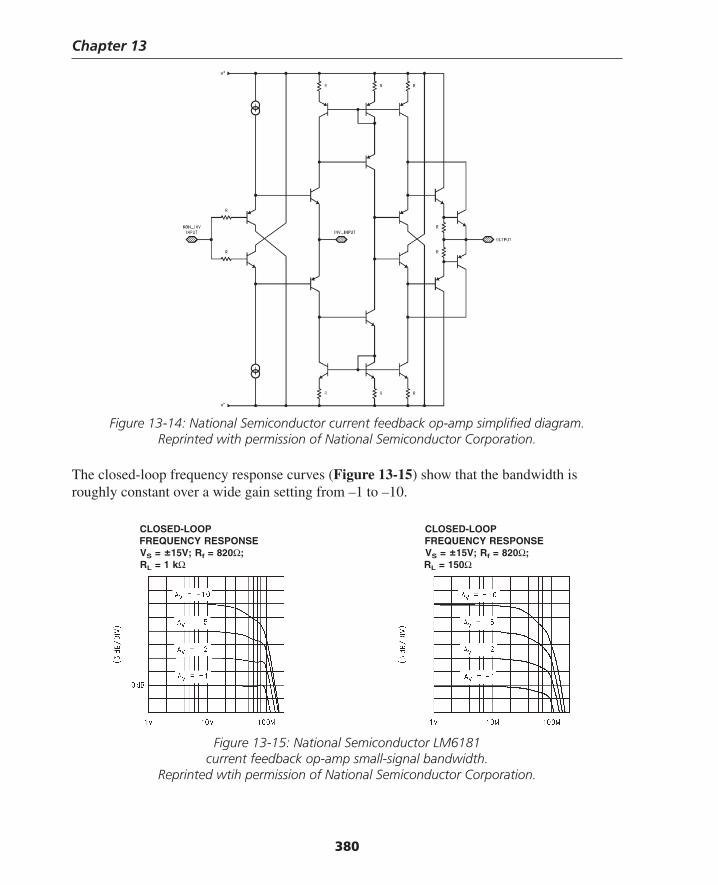
Chapter 13
380
Figure 13-14: National Semiconductor current feedback op-amp simplifi ed diagram.Reprinted with permission of National Semiconductor Corporation.
The closed-loop frequency response curves (Figure 13-15) show that the bandwidth is roughly constant over a wide gain setting from –1 to –10.
CLOSED-LOOPFREQUENCY RESPONSEVS = ±15V; Rf = 820Ω;RL = 1 kΩ
CLOSED-LOOPFREQUENCY RESPONSEVS = ±15V; Rf = 820Ω;RL = 150Ω
Figure 13-15: National Semiconductor LM6181 current feedback op-amp small-signal bandwidth.
Reprinted wtih permission of National Semiconductor Corporation.
Thompson Book.indb 380 3/20/2006 11:36:56 AM
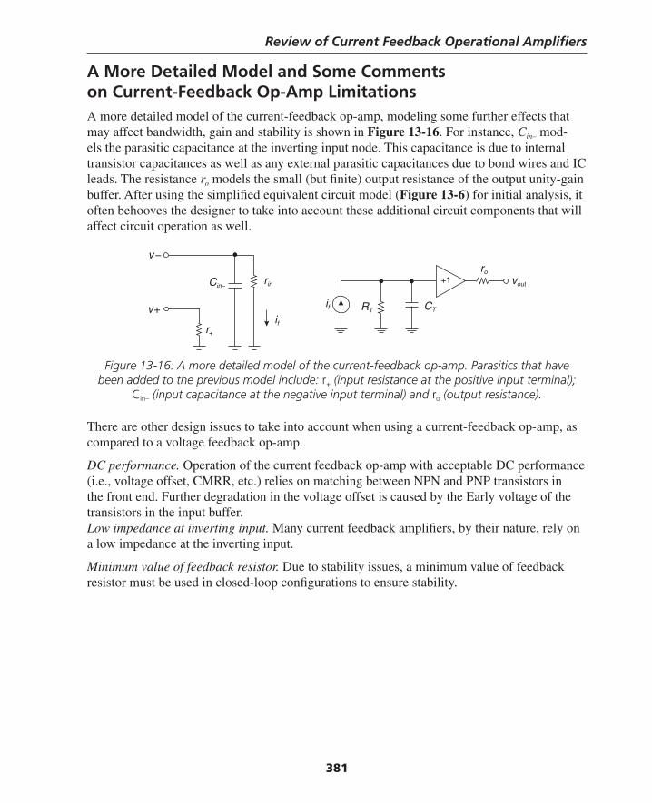
Review of Current Feedback Operational Amplifi ers
381
A More Detailed Model and Some Comments on Current-Feedback Op-Amp LimitationsA more detailed model of the current-feedback op-amp, modeling some further effects that may affect bandwidth, gain and stability is shown in Figure 13-16. For instance, Cin– mod-els the parasitic capacitance at the inverting input node. This capacitance is due to internal transistor capacitances as well as any external parasitic capacitances due to bond wires and IC leads. The resistance ro models the small (but fi nite) output resistance of the output unity-gain buffer. After using the simplifi ed equivalent circuit model (Figure 13-6) for initial analysis, it often behooves the designer to take into account these additional circuit components that will affect circuit operation as well.
Figure 13-16: A more detailed model of the current-feedback op-amp. Parasitics that have been added to the previous model include: r+ (input resistance at the positive input terminal);
Cin– (input capacitance at the negative input terminal) and ro (output resistance).
There are other design issues to take into account when using a current-feedback op-amp, as compared to a voltage feedback op-amp.
DC performance. Operation of the current feedback op-amp with acceptable DC performance (i.e., voltage offset, CMRR, etc.) relies on matching between NPN and PNP transistors in the front end. Further degradation in the voltage offset is caused by the Early voltage of the transistors in the input buffer.Low impedance at inverting input. Many current feedback amplifi ers, by their nature, rely on a low impedance at the inverting input.
Minimum value of feedback resistor. Due to stability issues, a minimum value of feedback resistor must be used in closed-loop confi gurations to ensure stability.
voutrin
if CTRTv+
v −ro
if
Cin−
r+
+1
Thompson Book.indb 381 3/20/2006 11:36:57 AM

382
Chapter 13 Problems
Problem 13.1Using a conventional op-amp model, draw a circuit using the 741 operational-amplifi er pro-viding a gain of +100. Find the bandwidth of this amplifi er circuit.
Problem 13.2Using the AD844 datasheet, extract current-feedback op-amp parameters and fi ll in the equivalent circuit model of Figure 13-6.
Problem 13.3Using open-circuit time constants, estimate the bandwidth of the four-transistor input circuit (Q1–Q4) of Figure 13-5. Assume that Q3 and Q4 are each biased at a collector current Io and that each transistor has a current gain-bandwidth product of ωT = 6.3 × 10⁹ radians/second. Assume that each transistor has Cμ = 0.5 pF, and assume that IB1 = IB2 = IO = 1 mA. Make other assumptions as needed and state them.
Problem 13.4Using the circuit of Figure 13-5, fi nd the collector current in transistors Q3 and Q4, assuming that the input transistors Q1 and Q2 are biased as shown. Assume that if = 0 and that the input v+ is grounded for purposes of this calculation. Furthermore, assume that the reverse satura-tion current is IS,NPN for Q2 and Q3, and is IS,PNP for Q1 and Q4.
Thompson Book.indb 382 3/20/2006 11:36:57 AM
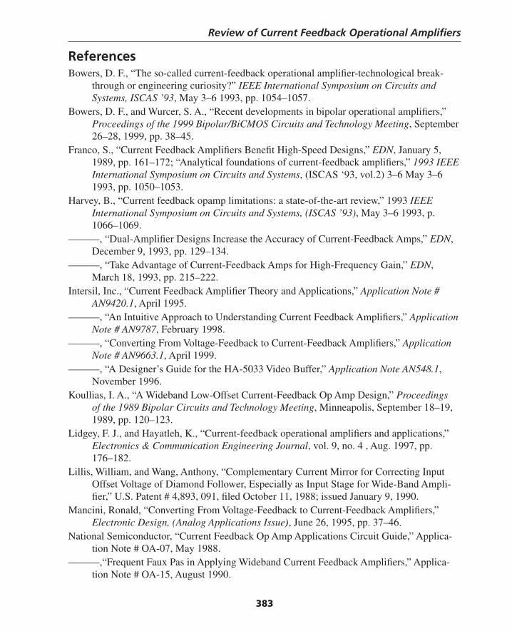
Review of Current Feedback Operational Amplifi ers
383
ReferencesBowers, D. F., “The so-called current-feedback operational amplifi er-technological break-
through or engineering curiosity?” IEEE International Symposium on Circuits and Systems, ISCAS ’93, May 3–6 1993, pp. 1054–1057.
Bowers, D. F., and Wurcer, S. A., “Recent developments in bipolar operational amplifi ers,” Proceedings of the 1999 Bipolar/BiCMOS Circuits and Technology Meeting, September 26–28, 1999, pp. 38–45.
Franco, S., “Current Feedback Amplifi ers Benefi t High-Speed Designs,” EDN, January 5, 1989, pp. 161–172; “Analytical foundations of current-feedback amplifi ers,” 1993 IEEE International Symposium on Circuits and Systems, (ISCAS ‘93, vol.2) 3–6 May 3–6 1993, pp. 1050–1053.
Harvey, B., “Current feedback opamp limitations: a state-of-the-art review,” 1993 IEEE International Symposium on Circuits and Systems, (ISCAS ’93), May 3–6 1993, p. 1066–1069.
———, “Dual-Amplifi er Designs Increase the Accuracy of Current-Feedback Amps,” EDN, December 9, 1993, pp. 129–134.
———, “Take Advantage of Current-Feedback Amps for High-Frequency Gain,” EDN, March 18, 1993, pp. 215–222.
Intersil, Inc., “Current Feedback Amplifi er Theory and Applications,” Application Note # AN9420.1, April 1995.
———, “An Intuitive Approach to Understanding Current Feedback Amplifi ers,” Application Note # AN9787, February 1998.
———, “Converting From Voltage-Feedback to Current-Feedback Amplifi ers,” Application Note # AN9663.1, April 1999.
———, “A Designer’s Guide for the HA-5033 Video Buffer,” Application Note AN548.1, November 1996.
Koullias, I. A., “A Wideband Low-Offset Current-Feedback Op Amp Design,” Proceedings of the 1989 Bipolar Circuits and Technology Meeting, Minneapolis, September 18–19, 1989, pp. 120–123.
Lidgey, F. J., and Hayatleh, K., “Current-feedback operational amplifi ers and applications,” Electronics & Communication Engineering Journal, vol. 9, no. 4 , Aug. 1997, pp. 176–182.
Lillis, William, and Wang, Anthony, “Complementary Current Mirror for Correcting Input Offset Voltage of Diamond Follower, Especially as Input Stage for Wide-Band Ampli-fi er,” U.S. Patent # 4,893, 091, fi led October 11, 1988; issued January 9, 1990.
Mancini, Ronald, “Converting From Voltage-Feedback to Current-Feedback Amplifi ers,” Electronic Design, (Analog Applications Issue), June 26, 1995, pp. 37–46.
National Semiconductor, “Current Feedback Op Amp Applications Circuit Guide,” Applica-tion Note # OA-07, May 1988.
———,“Frequent Faux Pas in Applying Wideband Current Feedback Amplifi ers,” Applica-tion Note # OA-15, August 1990.
Thompson Book.indb 383 3/20/2006 11:36:57 AM
Chapter 13
384
———, “Current-Feedback Myths Debunked,” Application Note # OA-20, July 1992. ———, “Current Feedback Amplifi ers,” Application Note # OA-31, November 1992. ———, “Current Feedback Loop Gain Analysis and Performance Enhancement,” Application
Note # OA-13, January 1993. ———, “Stability Analysis of Current Feedback Amplifi ers,” Application Note # OA-25,
May 1995. ———,“Current vs. Voltage Feedback Amplifi ers,” Application Note # OA-30, January 1998.Palumbo, G., “Current feedback amplifi er: stability and compensation,” Proceedings of the
40th Midwest Symposium on Circuits and Systems, August 3-6, 1997, pp. 249-252.Palumbo, G., and Pennisi, S., “Current-feedback amplifi ers versus voltage operational am-
plifi ers,” IEEE Transactions on Circuits and Systems I: Fundamental Theory and Applications, vol. 48, no. 5, May 2001, pp. 617–623.
Sauerwald, M., “Current feedback and voltage feedback. The choice amplifi ers: which one to use, when and why,” Northcon/94 Conference Record, October 11–13, 1994, pp. 285–289.
Smith, Doug, “Current-feedback amps enhance active-fi lter speed and performance,” EDN, September 17, 1990, pp. 167–172.
Smith, Douglas, “High Speed Operational Amplifi er Architectures,” Proceedings of the 1993 IEEE Bipolar Circuits and Technology Meeting, pp. 141–148.
Smith, Doug, Koen, Mike, and Witulski, Arthur, “Evolution of High-Speed Operational Amplifi er Architectures,” IEEE Journal of Solid-State Circuits, vol. 29, no. 10, October 1994, pp. 1166–1179.
Tammam, A. A., Hayatleh, K., Hart, B., and Lidgey, F. J., “High Performance Current-Feed-back Op-Amps,” Proceedings of the 2004 International Symposium on Circuits and Systems, ( ISCAS ’04), May 23–26, 2004, pp. 825–828.
Texas Instruments, Inc., “Voltage Feedback vs. Current Feedback Op Amps Applications Report,” TI Application Note, November 1998.
Toumazou, Chris, Payne, Alison, and Lidgey, John, “Current-Feedback Versus Voltage Feedback Amplifi ers: History, Insight and Relationships,” 1993 IEEE International Symposium on Circuits and Systems, (ISCAS ’93), May 3–6, 1993, pp. 1046–1049.
Wilson, B., “Current-mode amplifi ers,” IEEE International Symposium on Circuits and Sys-tems, May 8–11, 1989, pp. 1576–1579.
Wong, James, “Current-Feedback Op Amps Extend High Frequency Performance,” EDN, October 26, 1989, pp. 211–216.
Thompson Book.indb 384 3/20/2006 11:36:57 AM

385
C H A P T E R 14Analog Low-Pass Filters
IntroductionThe low-pass fi lter is a ubiquitous component in many different kinds of signal-processing systems. Channel-separation, A/D antialiasing, and general signal processing are applications for low-pass fi lters, just to name a few. Even if you are a digital fi lter designer, it behooves you to know something about analog fi lter design, since many digital fi lters begin as analog pro-totypes, and are then transformed to the digital domain. Also, DSP systems generally have an analog front end that includes an analog low-pass fi lter for antialiasing purposes (Figure 14-1).
As with any kind of design, the “devil is in the details.” Your specifi cation will lead you to choices in fi lter topology and fi lter order, depending on the attenuation you need, the ripple that you can live with, and also the group delay variation that you can live with. In the follow-ing sections, we discuss design issues associated with low-pass fi lter design. The results can be extended without much trouble to band-pass and high-pass fi lters as well.
In This Chapter
The basics of analog low-pass fi ltering are discussed. These techniques are useful for designing analog fi lters as well as prototypes used for digital fi lters. This chapter is by no means an all-inclusive tutorial on analog circuit design; rather it is introductory in nature and the reader is referred to other texts for more details, if necessary.
Figure 14-1: Typical digital signal-processing chain.
AnalogInputSignal
AnalogLow-passFilter
A/DConversion
DigitalFilter
DigitalOutput
DigitalInput
Thompson Book.indb 385 3/20/2006 11:36:58 AM

Chapter 14
386
Review of Low-Pass Filter BasicsThe magnitude response of the ideal low-pass fi lter is shown in Figure 14-2a. The gain of this fi lter is perfectly fl at in the passband (for frequencies less than the fi lter cutoff1 frequency ωh), and the response drops to zero for frequencies higher than the cutoff frequency.
The magnitude response of a real-world low-pass fi lter is shown in Figure 14-2b. The non-ideal effects include:
• Possible ripple in the fi lter passband.
• Possible maximum attenuation fl oor in the stopband.
• Finite transition width between passband and stopband.
1 In general, the cutoff frequency of a fi lter is specifi ed to be the frequency at which the gain through the fi lter has dropped to 0.707 of the DC value, or –3dB.
ω
ω
ω
ω
�(ω)
G(ω)
ωp ωS
PASSBAND
STOPBAND
STOPBAND
PASSBAND
TRANSITION BAND
h(jω) h(jω)
(a) (b)
(c) (d)
Figure 14-2: Response of low-pass fi lter. (a) Ideal low-pass fi lter magnitude ⏐H(jω)⏐. (b) Real-world magnitude response ⏐H(jω)⏐showing possible ripple in the passband
and stopband, and a fi nite transition width between passband and stopband. (c) Ideal low-pass fi lter phase response ∠(ω) showing a negative phase shift that increases
linearly with frequency. (d) Ideal low-pass fi lter group delay response G(ω) which is constant.
Thompson Book.indb 386 3/20/2006 11:36:58 AM
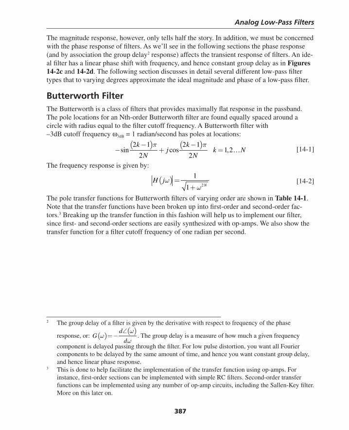
Analog Low-Pass Filters
387
The magnitude response, however, only tells half the story. In addition, we must be concerned with the phase response of fi lters. As we’ll see in the following sections the phase response (and by association the group delay2 response) affects the transient response of fi lters. An ide-al fi lter has a linear phase shift with frequency, and hence constant group delay as in Figures 14-2c and 14-2d. The following section discusses in detail several different low-pass fi lter types that to varying degrees approximate the ideal magnitude and phase of a low-pass fi lter.
Butterworth FilterThe Butterworth is a class of fi lters that provides maximally fl at response in the passband. The pole locations for an Nth-order Butterworth fi lter are found equally spaced around a circle with radius equal to the fi lter cutoff frequency. A Butterworth fi lter with –3dB cutoff frequency ω3dB = 1 radian/second has poles at locations:
( ) ( )2 1 2 1
sin cos 1,22 2
k kj k N
N N
π π− −− + = … [14-1]
The frequency response is given by:
( )2
1
1 NH jω
ω=
+ [14-2]
The pole transfer functions for Butterworth fi lters of varying order are shown in Table 14-1. Note that the transfer functions have been broken up into fi rst-order and second-order fac-tors.3 Breaking up the transfer function in this fashion will help us to implement our fi lter, since fi rst- and second-order sections are easily synthesized with op-amps. We also show the transfer function for a fi lter cutoff frequency of one radian per second.
2 The group delay of a fi lter is given by the derivative with respect to frequency of the phase
response, or: ( )( )d
Gd
ωω
ω
∠= − . The group delay is a measure of how much a given frequency
component is delayed passing through the fi lter. For low pulse distortion, you want all Fourier components to be delayed by the same amount of time, and hence you want constant group delay, and hence linear phase response.
3 This is done to help facilitate the implementation of the transfer function using op-amps. For instance, fi rst-order sections can be implemented with simple RC fi lters. Second-order transfer functions can be implemented using any number of op-amp circuits, including the Sallen-Key fi lter. More on this later on.
Thompson Book.indb 387 3/20/2006 11:36:58 AM
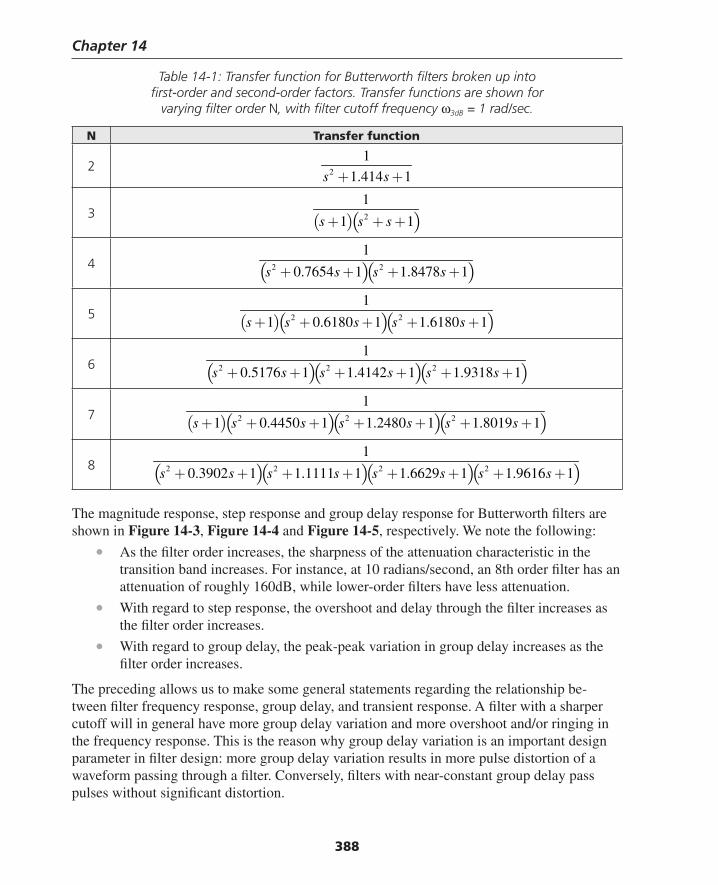
Chapter 14
388
Table 14-1: Transfer function for Butterworth fi lters broken up into fi rst-order and second-order factors. Transfer functions are shown for
varying fi lter order N, with fi lter cutoff frequency ω3dB = 1 rad/sec.
N Transfer function
2 2
1
1.414 1s s+ +
3 ( )( )2
1
1 1s s s+ + +
4 ( )( )2 2
1
0.7654 1 1.8478 1s s s s+ + + +
5 ( )( )( )2 2
1
1 0.6180 1 1.6180 1s s s s s+ + + + +
6 ( )( )( )2 2 2
1
0.5176 1 1.4142 1 1.9318 1s s s s s s+ + + + + +
7 ( )( )( )( )2 2 2
1
1 0.4450 1 1.2480 1 1.8019 1s s s s s s s+ + + + + + +
8 ( )( )( )( )2 2 2 2
1
0.3902 1 1.1111 1 1.6629 1 1.9616 1s s s s s s s s+ + + + + + + +
The magnitude response, step response and group delay response for Butterworth fi lters are shown in Figure 14-3, Figure 14-4 and Figure 14-5, respectively. We note the following:
• As the fi lter order increases, the sharpness of the attenuation characteristic in the transition band increases. For instance, at 10 radians/second, an 8th order fi lter has an attenuation of roughly 160dB, while lower-order fi lters have less attenuation.
• With regard to step response, the overshoot and delay through the fi lter increases as the fi lter order increases.
• With regard to group delay, the peak-peak variation in group delay increases as the fi lter order increases.
The preceding allows us to make some general statements regarding the relationship be-tween fi lter frequency response, group delay, and transient response. A fi lter with a sharper cutoff will in general have more group delay variation and more overshoot and/or ringing in the frequency response. This is the reason why group delay variation is an important design parameter in fi lter design: more group delay variation results in more pulse distortion of a waveform passing through a fi lter. Conversely, fi lters with near-constant group delay pass pulses without signifi cant distortion.
Thompson Book.indb 388 3/20/2006 11:36:59 AM
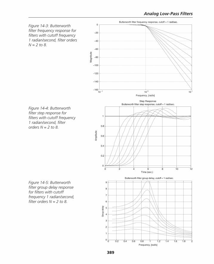
Analog Low-Pass Filters
389
Figure 14-4: Butterworth fi lter step response for fi lters with cutoff frequency 1 radian/second, fi lter orders N = 2 to 8.
Mag
nitu
de10 −1 10 0 10 1
−160
−140
−120
−100
−80
−60
−40
−20
0Butterworth filter frequency response, cutoff = 1 rad/sec.
Frequency, [rad/s]
Figure 14-3: Butterworth fi lter frequency response for fi lters with cutoff frequency 1 radian/second, fi lter orders N = 2 to 8.
Time (sec.)
Am
plitu
de
Step Response
0 2 4 6 8 10 120
0.2
0.4
0.6
0.8
1
Butterworth filter step response, cutoff = 1 rad/sec.
0 0.2 0.4 0.6 0.8 1 1.2 1.4 1.6 1.8 20
1
2
3
4
5
6
7
8
9
Butterworth filter group delay, cutoff = 1 rad/sec.
Frequency, [rad/s]
Gro
up d
elay
Figure 14-5: Butterworth fi lter group delay response for fi lters with cutoff frequency 1 radian/second, fi lter orders N = 2 to 8.
Thompson Book.indb 389 3/20/2006 11:37:00 AM
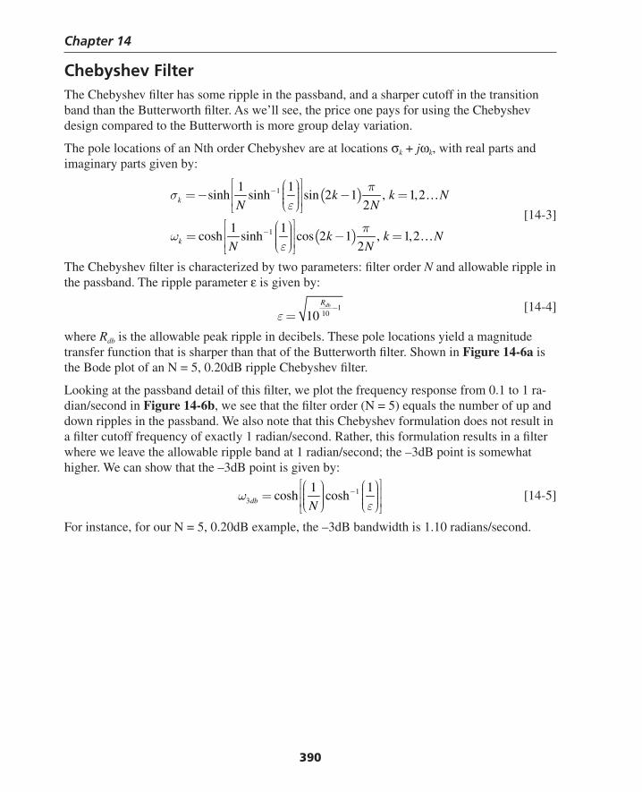
Chapter 14
390
Chebyshev FilterThe Chebyshev fi lter has some ripple in the passband, and a sharper cutoff in the transition band than the Butterworth fi lter. As we’ll see, the price one pays for using the Chebyshev design compared to the Butterworth is more group delay variation.
The pole locations of an Nth order Chebyshev are at locations σk + jωk, with real parts and imaginary parts given by:
( )
( )
1
1
1 1sinh sinh sin 2 1 , 1,2
2
1 1cosh sinh cos 2 1 , 1,2
2
k
k
k k NN N
k k NN N
πσ
ε
πω
ε
−
−
⎡ ⎤⎛ ⎞⎟⎜⎢ ⎥= − − =⎟⎜ ⎟⎜⎢ ⎥⎝ ⎠⎣ ⎦⎡ ⎤⎛ ⎞⎟⎜⎢ ⎥= − =⎟⎜ ⎟⎜⎢ ⎥⎝ ⎠⎣ ⎦
…
… [14-3]
The Chebyshev fi lter is characterized by two parameters: fi lter order N and allowable ripple in the passband. The ripple parameter ε is given by:
11010
dbR
ε−
= [14-4]
where Rdb is the allowable peak ripple in decibels. These pole locations yield a magnitude transfer function that is sharper than that of the Butterworth fi lter. Shown in Figure 14-6a is the Bode plot of an N = 5, 0.20dB ripple Chebyshev fi lter.
Looking at the passband detail of this fi lter, we plot the frequency response from 0.1 to 1 ra-dian/second in Figure 14-6b, we see that the fi lter order (N = 5) equals the number of up and down ripples in the passband. We also note that this Chebyshev formulation does not result in a fi lter cutoff frequency of exactly 1 radian/second. Rather, this formulation results in a fi lter where we leave the allowable ripple band at 1 radian/second; the –3dB point is somewhat higher. We can show that the –3dB point is given by:
13
1 1cosh coshdb N
ωε
−⎡ ⎤⎛ ⎞ ⎛ ⎞⎟ ⎟⎜ ⎜⎢ ⎥= ⎟ ⎟⎜ ⎜⎟ ⎟⎜ ⎜⎢ ⎥⎝ ⎠ ⎝ ⎠⎣ ⎦
[14-5]
For instance, for our N = 5, 0.20dB example, the –3dB bandwidth is 1.10 radians/second.
Thompson Book.indb 390 3/20/2006 11:37:01 AM
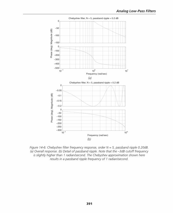
Analog Low-Pass Filters
391
(a)Frequency (rad/sec)
Pha
se (
deg)
; Mag
nitu
de (
dB)
Chebyshev filter, N = 5, passband ripple = 0.2 dB
−150
−100
−50
0
10−1
100
101
−500
−400
−300
−200
−100
0
Frequency (rad/sec)
Pha
se (
deg)
; Mag
nitu
de (
dB)
Chebyshev filter, N = 5, passband ripple = 0.2 dB
−0.2
−0.15
−0.1
−0.05
0
10−1 010−300
−250
−200
−150
−100
−50
0
(b)
Figure 14-6: Chebyshev fi lter frequency response, order N = 5, passband ripple 0.20dB. (a) Overall response. (b) Detail of passband ripple. Note that the –3dB cutoff frequency
is slightly higher than 1 radian/second. The Chebyshev approximation shown here results in a passband ripple frequency of 1 radian/second.
Thompson Book.indb 391 3/20/2006 11:37:02 AM
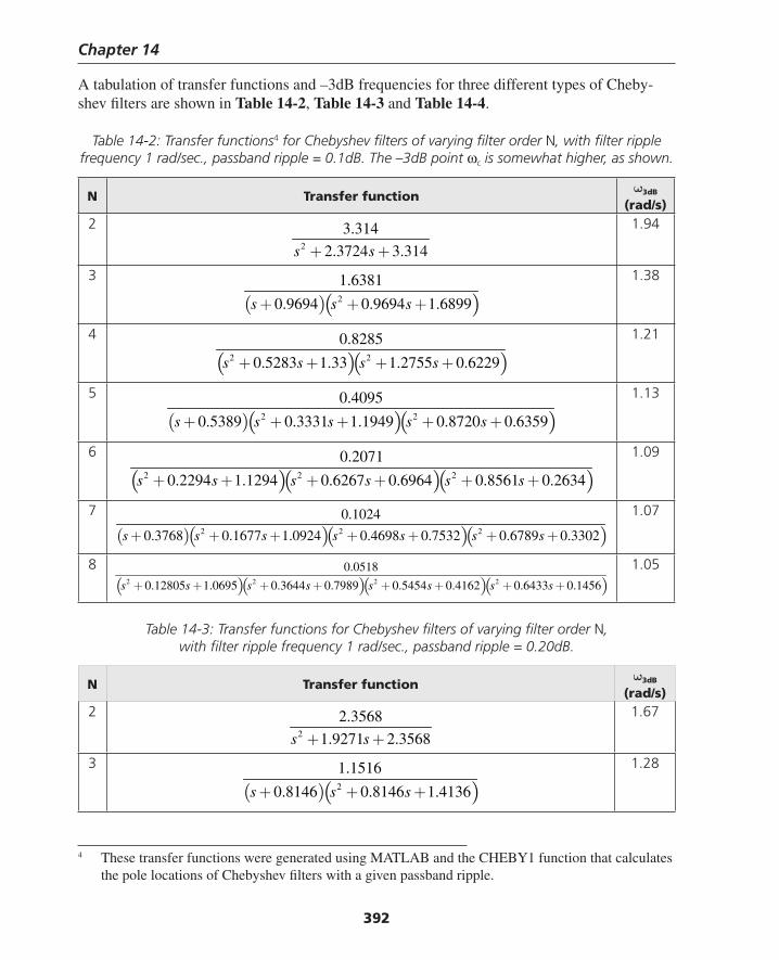
Chapter 14
392
A tabulation of transfer functions and –3dB frequencies for three different types of Cheby-shev fi lters are shown in Table 14-2, Table 14-3 and Table 14-4.
Table 14-2: Transfer functions4 for Chebyshev fi lters of varying fi lter order N, with fi lter ripple frequency 1 rad/sec., passband ripple = 0.1dB. The –3dB point ωc is somewhat higher, as shown.
N Transfer functionω3dB
(rad/s)2
2
3.314
2.3724 3.314s s+ +
1.94
3
( )( )2
1.6381
0.9694 0.9694 1.6899s s s+ + +
1.38
4
( )( )2 2
0.8285
0.5283 1.33 1.2755 0.6229s s s s+ + + +
1.21
5
( )( )( )2 2
0.4095
0.5389 0.3331 1.1949 0.8720 0.6359s s s s s+ + + + +
1.13
6
( )( )( )2 2 2
0.2071
0.2294 1.1294 0.6267 0.6964 0.8561 0.2634s s s s s s+ + + + + +
1.09
7
( )( )( )( )2 2 2
0.1024
0.3768 0.1677 1.0924 0.4698 0.7532 0.6789 0.3302s s s s s s s+ + + + + + +
1.07
8
( )( )( )( )2 2 2 2
0.0518
0.12805 1.0695 0.3644 0.7989 0.5454 0.4162 0.6433 0.1456s s s s s s s s+ + + + + + + +
1.05
Table 14-3: Transfer functions for Chebyshev fi lters of varying fi lter order N, with fi lter ripple frequency 1 rad/sec., passband ripple = 0.20dB.
N Transfer functionω3dB
(rad/s)2
2
2.3568
1.9271 2.3568s s+ +
1.67
3
( )( )2
1.1516
0.8146 0.8146 1.4136s s s+ + +
1.28
4 These transfer functions were generated using MATLAB and the CHEBY1 function that calculates the pole locations of Chebyshev fi lters with a given passband ripple.
Thompson Book.indb 392 3/20/2006 11:37:02 AM
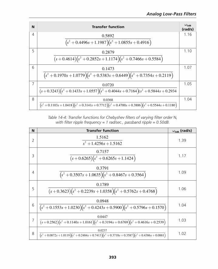
Analog Low-Pass Filters
393
N Transfer functionω3dB
(rad/s)4
( )( )2 2
0.5892
0.4496 1.1987 1.0855 0.4916s s s s+ + + +
1.16
5
( )( )( )2 2
0.2879
0.4614 0.2852 1.1174 0.7466 0.5584s s s s s+ + + + +
1.10
6
( )( )( )2 2 2
0.1473
0.1970 1.0779 0.5383 0.6449 0.7354 0.2119s s s s s s+ + + + + +
1.07
7
( )( )( )2 2 2
0.0720
0.3243 0.1433 1.0557 0.4044 0.7164 ( 0.5844 0.2934s s s s s s s+ + + + + + +
1.05
8
( )( )( )( )2 2 2 2
0.0368
0.1103 1.0418 0.3141 0.7712 0.4700 0.3886 0.5544 0.1180s s s s s s s s+ + + + + + + +
1.04
Table 14-4: Transfer functions for Chebyshev fi lters of varying fi lter order N, with fi lter ripple frequency = 1 rad/sec., passband ripple = 0.50dB.
N Transfer function ω3dB (rad/s)
2 2
1.5162
1.4256 1.5162s s+ +1.39
3 ( )( )2
0.7157
0.6265 0.6265 1.1424s s s+ + + 1.17
4 ( )( )2 2
0.3791
0.3507 1.0635 0.8467 0.3564s s s s+ + + + 1.09
5 ( )( )( )2 2
0.1789
0.3623 0.2239 1.0358 0.5762 0.4768s s s s s+ + + + + 1.06
6 ( )( )( )2 2 2
0.0948
0.1553 1.0230 0.4243 0.5900 0.5796 0.1570s s s s s s+ + + + + + 1.04
7 ( )( )( )( )2 2 2
0.0447
0.2562 0.1140 1.0161 0.3194 0.6769 0.4616 0.2539s s s s s s s+ + + + + + + 1.03
8 ( )( )( )( )2 2 2 2
0.0237
0.0872 1.0119 0.2484 0.7413 0.3718 0.3587 0.4386 0.0881s s s s s s s s+ + + + + + + + 1.02
Thompson Book.indb 393 3/20/2006 11:37:03 AM
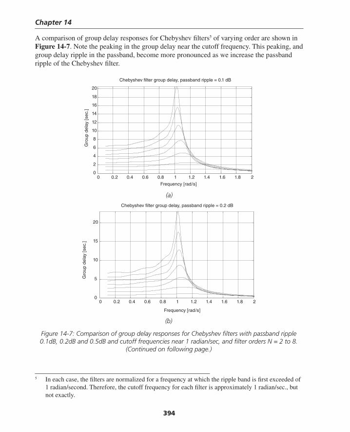
Chapter 14
394
A comparison of group delay responses for Chebyshev fi lters5 of varying order are shown in Figure 14-7. Note the peaking in the group delay near the cutoff frequency. This peaking, and group delay ripple in the passband, become more pronounced as we increase the passband ripple of the Chebyshev fi lter.
5 In each case, the fi lters are normalized for a frequency at which the ripple band is fi rst exceeded of 1 radian/second. Therefore, the cutoff frequency for each fi lter is approximately 1 radian/sec., but not exactly.
(a)
0 0.2 0.4 0.6 0.8 1 1.2 1.4 1.6 1.8 20
2
4
6
8
10
12
14
16
18
20
Chebyshev filter group delay, passband ripple = 0.1 dBG
roup
del
ay [
sec.
]
Frequency [rad/s]
(b)
Figure 14-7: Comparison of group delay responses for Chebyshev fi lters with passband ripple 0.1dB, 0.2dB and 0.5dB and cutoff frequencies near 1 radian/sec, and fi lter orders N = 2 to 8.
(Continued on following page.)
0 0.2 0.4 0.6 0.8 1 1.2 1.4 1.6 1.8 20
5
10
15
20
Chebyshev filter group delay, passband ripple = 0.2 dB
Frequency [rad/s]
Gro
up d
elay
[se
c.]
Thompson Book.indb 394 3/20/2006 11:37:04 AM
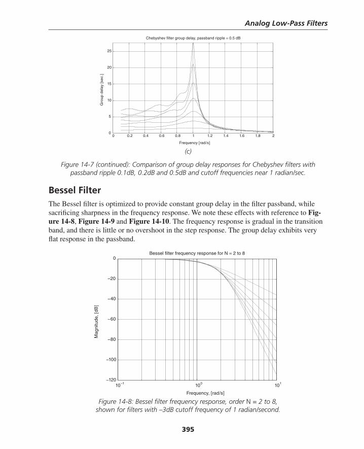
Analog Low-Pass Filters
395
(c)
Figure 14-7 (continued): Comparison of group delay responses for Chebyshev fi lters with passband ripple 0.1dB, 0.2dB and 0.5dB and cutoff frequencies near 1 radian/sec.
Bessel FilterThe Bessel fi lter is optimized to provide constant group delay in the fi lter passband, while sacrifi cing sharpness in the frequency response. We note these effects with reference to Fig-ure 14-8, Figure 14-9 and Figure 14-10. The frequency response is gradual in the transition band, and there is little or no overshoot in the step response. The group delay exhibits very fl at response in the passband.
0 0.2 0.4 0.6 0.8 1 1.2 1.4 1.6 1.8 20
5
10
15
20
25
Chebyshev filter group delay, passband ripple = 0.5 dB
Frequency [rad/s]
Gro
up d
elay
[se
c.]
Figure 14-8: Bessel fi lter frequency response, order N = 2 to 8, shown for fi lters with –3dB cutoff frequency of 1 radian/second.
10−1 100 101−120
−100
−80
−60
−40
−20
0Bessel filter frequency response for N = 2 to 8
Frequency, [rad/s]
Mag
nitu
de, [
dB]
Thompson Book.indb 395 3/20/2006 11:37:05 AM
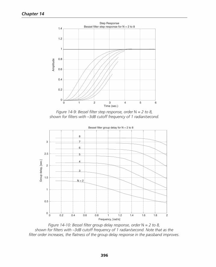
Chapter 14
396
Figure 14-9: Bessel fi lter step response, order N = 2 to 8, shown for fi lters with –3dB cutoff frequency of 1 radian/second.
Time (sec.)
Am
plitu
de
Step ResponseBessel filter step response for N = 2 to 8
0 1 2 3 4 5 60
0.2
0.4
0.6
0.8
1
1.2
1.4
Figure 14-10: Bessel fi lter group delay response, order N = 2 to 8, shown for fi lters with –3dB cutoff frequency of 1 radian/second. Note that as the
fi lter order increases, the fl atness of the group delay response in the passband improves.
0 0.2 0.4 0.6 0.8 1 1.2 1.4 1.6 1.8 20
0.5
1
1.5
2
2.5
3
N = 2
3
4
5
6
7
8
Bessel filter group delay for N = 2 to 8
Frequency, [rad/s]
Gro
up d
elay
, [se
c.]
Thompson Book.indb 396 3/20/2006 11:37:05 AM
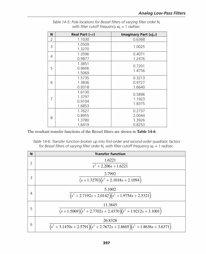
Analog Low-Pass Filters
397
Table 14-5: Pole locations for Bessel fi lters of varying fi lter order N, with fi lter cutoff frequency ωc = 1 rad/sec.
N Real Part (–σ) Imaginary Part (±jω)2 1.1030 0.6368
31.05091.3270
1.0025
41.35960.9877
0.40711.2476
51.38510.96061.5069
0.72011.4756
61.57351.38360.9318
0.32130.97271.6640
7
1.61301.37970.91041.6853
0.58961.19231.8375
8
1.76270.89551.37801.6419
0.27372.00441.39260.8253
The resultant transfer functions of the Bessel fi lters are shown in Table 14-6.
Table 14-6: Transfer function broken up into fi rst-order and second-order quadratic factors for Bessel fi lters of varying fi lter order N, with fi lter cutoff frequency ωc = 1 rad/sec.
N Transfer function
2 2
1.6221
2.206 1.6221s s+ +
3 ( )( )2
2.7992
1.3270 2.1018 2.1094s s s+ + +
4 ( )( )2 2
5.1002
2.7192 2.0142 1.9754 2.5321s s s s+ + + +
5 ( )( )( )2 2
11.3845
1.5069 2.7702 2.4370 1.9212 3.1001s s s s s+ + + + +
6 ( )( )( )2 2 2
26.8328
3.1470 2.5791 2.7672 2.8605 1.8636 3.6371s s s s s s+ + + + + +
Thompson Book.indb 397 3/20/2006 11:37:06 AM
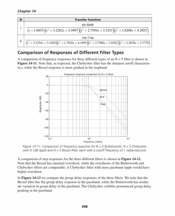
Chapter 14
398
N Transfer function
7 ( )( )( )( )2 2 2
69.5099
1.6853 3.2262 2.9497 2.7594 3.3251 1.8208 4.2052s s s s s s s+ + + + + + +
8 ( )( )( )( )2 2 2 2
198.7746
3.5254 3.1820 1.7910 4.1895 2.7560 3.8382 3.2838 3.3770s s s s s s s s+ + + + + + + +
Comparison of Responses of Different Filter TypesA comparison of frequency responses for three different types of an N = 5 fi lter is shown in Figure 14-11. Note that, as expected, the Chebyshev fi lter has the sharpest cutoff characteris-tics, while the Bessel response is more gradual in the stopband.
Figure 14-11: Comparison of frequency response for N = 5 Butterworth, N = 5 Chebyshev with 0.1dB ripple and N = 5 Bessel fi lter, each with a cutoff frequency of 1 radian/second.
A comparison of step responses for the three different fi lters is shown in Figure 14-12. Note that the Bessel has minimal overshoot, while the overshoots of the Butterworth and Chebyshev fi lters are comparable. A Chebyshev fi lter with more passband ripple would have higher overshoot.
In Figure 14-13 we compare the group delay responses of the three fi lters. We note that the Bessel fi lter has fl at group delay response in the passband, while the Butterworth has moder-ate variation in group delay in the passband. The Chebyshev exhibits pronounced group delay peaking in the passband.
10 −1 10 0 10 1−120
−100
−80
−60
−40
−20
0
20Frequency response comparison for N = 5 filters
Frequency, [rad/s]
Mag
nitu
de, [
dB]
Bessel
Butt
Cheb
Thompson Book.indb 398 3/20/2006 11:37:06 AM
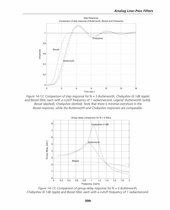
Analog Low-Pass Filters
399
Figure 14-12: Comparison of step response for N = 5 Butterworth, Chebyshev (0.1dB ripple) and Bessel fi lter, each with a cutoff frequency of 1 radian/second. Legend: Butterworth (solid),
Bessel (dashed), Chebyshev (dotted). Note that there is minimal overshoot in the Bessel response, while the Butterworth and Chebyshev responses are comparable.
Time (sec.)
Am
plitu
de
Step Response
0 3 6 9 12 15 18
0
0.2
0.4
0.6
0.8
1
Comparison of step response of Butterworth, Bessel and Chebyshev
Bessel
Chebyshev
Butterworth
Figure 14-13: Comparison of group delay response for N = 5 Butterworth, Chebyshev (0.1dB ripple) and Bessel fi lter, each with a cutoff frequency of 1 radian/second.
0 0.2 0.4 0.6 0.8 1 1.2 1.4 1.6 1.8 20
1
2
3
4
5
6
7
8
Butterworth
Bessel
Chebyshev 0.1dB
Group delay comparison for N = 5 filters
Frequency, [rad/s]
Gro
up d
elay
, [se
c.]
Thompson Book.indb 399 3/20/2006 11:37:07 AM
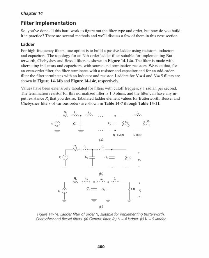
Chapter 14
400
Filter ImplementationSo, you’ve done all this hard work to fi gure out the fi lter type and order, but how do you build it in practice? There are several methods and we’ll discuss a few of them in this next section.
LadderFor high-frequency fi lters, one option is to build a passive ladder using resistors, inductors and capacitors. The topology for an Nth-order ladder fi lter suitable for implementing But-terworth, Chebyshev and Bessel fi lters is shown in Figure 14-14a. The fi lter is made with alternating inductors and capacitors, with source and termination resistors. We note that, for an even-order fi lter, the fi lter terminates with a resistor and capacitor and for an odd-order fi lter the fi lter terminates with an inductor and resistor. Ladders for N = 4 and N = 5 fi lters are shown in Figure 14-14b and Figure 14-14c, respectively.
Values have been extensively tabulated for fi lters with cutoff frequency 1 radian per second. The termination resistor for this normalized fi lter is 1.0 ohms, and the fi lter can have any in-put resistance Rs that you desire. Tabulated ladder element values for Butterworth, Bessel and Chebyshev fi lters of various orders are shown in Table 14-7 through Table 14-11.
(a)
vi
C2
RS
C4
L1 L3 L5
1.0
1.0C4C2
RS L1 L3
vi
vi C2 CnRT
1.0
RS L1 L3
RT
1.0
vo
+
−
Ln
N EVEN N ODD
…
…
vo
+
−
+−
+−
+−
(b)
(c)
Figure 14-14: Ladder fi lter of order N, suitable for implementing Butterworth, Chebyshev and Bessel fi lters. (a) Generic fi lter. (b) N = 4 ladder. (c) N = 5 ladder.
Thompson Book.indb 400 3/20/2006 11:37:08 AM
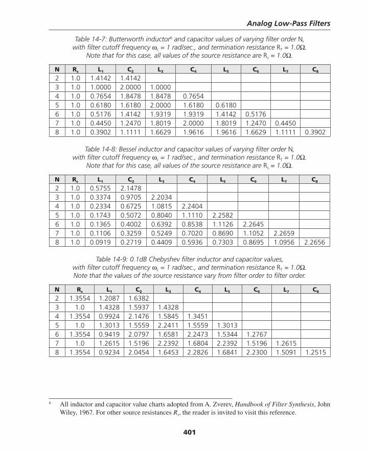
Analog Low-Pass Filters
401
Table 14-7: Butterworth inductor6 and capacitor values of varying fi lter order N, with fi lter cutoff frequency ωc = 1 rad/sec., and termination resistance RT = 1.0Ω.
Note that for this case, all values of the source resistance are Rs = 1.0Ω.
N Rs L1 C2 L3 C4 L5 C6 L7 C8
2 1.0 1.4142 1.41423 1.0 1.0000 2.0000 1.00004 1.0 0.7654 1.8478 1.8478 0.76545 1.0 0.6180 1.6180 2.0000 1.6180 0.61806 1.0 0.5176 1.4142 1.9319 1.9319 1.4142 0.51767 1.0 0.4450 1.2470 1.8019 2.0000 1.8019 1.2470 0.44508 1.0 0.3902 1.1111 1.6629 1.9616 1.9616 1.6629 1.1111 0.3902
Table 14-8: Bessel inductor and capacitor values of varying fi lter order N, with fi lter cutoff frequency ωc = 1 rad/sec., and termination resistance RT = 1.0Ω.
Note that for this case, all values of the source resistance are Rs = 1.0Ω.
N Rs L1 C2 L3 C4 L5 C6 L7 C8
2 1.0 0.5755 2.14783 1.0 0.3374 0.9705 2.20344 1.0 0.2334 0.6725 1.0815 2.24045 1.0 0.1743 0.5072 0.8040 1.1110 2.25826 1.0 0.1365 0.4002 0.6392 0.8538 1.1126 2.26457 1.0 0.1106 0.3259 0.5249 0.7020 0.8690 1.1052 2.26598 1.0 0.0919 0.2719 0.4409 0.5936 0.7303 0.8695 1.0956 2.2656
Table 14-9: 0.1dB Chebyshev fi lter inductor and capacitor values, with fi lter cutoff frequency ωc = 1 rad/sec., and termination resistance RT = 1.0Ω. Note that the values of the source resistance vary from fi lter order to fi lter order.
N Rs L1 C2 L3 C4 L5 C6 L7 C8
2 1.3554 1.2087 1.63823 1.0 1.4328 1.5937 1.43284 1.3554 0.9924 2.1476 1.5845 1.34515 1.0 1.3013 1.5559 2.2411 1.5559 1.30136 1.3554 0.9419 2.0797 1.6581 2.2473 1.5344 1.27677 1.0 1.2615 1.5196 2.2392 1.6804 2.2392 1.5196 1.26158 1.3554 0.9234 2.0454 1.6453 2.2826 1.6841 2.2300 1.5091 1.2515
6 All inductor and capacitor value charts adopted from A. Zverev, Handbook of Filter Synthesis, John Wiley, 1967. For other source resistances Rs, the reader is invited to visit this reference.
Thompson Book.indb 401 3/20/2006 11:37:08 AM

Chapter 14
402
Table 14-10: 0.25dB Chebyshev fi lter inductor and capacitor values, with fi lter cutoff frequency ωc = 1 rad/sec., and termination resistance RT = 1.0Ω.
N Rs L1 C2 L3 C4 L5 C6 L7 C8
2 2.0 0.6552 2.76323 1.0 1.6325 1.4360 1.63254 2.0 0.6747 3.6860 1.0247 1.88065 1.0 1.5046 1.4436 2.4050 1.4436 1.50466 2.0 0.6867 3.2074 0.9308 3.8102 1.2163 1.70887 1.0 1.5120 1.4169 2.4535 1.5350 2.4535 1.4169 1.5120
Table 14-11: 0.5dB Chebyshev fi lter inductor and capacitor values, with fi lter cutoff frequency ωc = 1 rad/sec., and termination resistance RT = 1.0Ω.
N Rs L1 C2 L3 C4 L5 C6 L7 C8
2 1.9841 0.9827 1.94973 1.0 1.8636 1.2804 1.86364 1.9841 0.9202 2.5864 1.3036 1.82585 1.0 1.8068 1.3025 2.6912 1.3025 1.80686 1.9841 0.9053 2.5774 1.3675 2.7133 1.2991 1.79617 1.0 1.7896 1.2961 2.7177 1.3848 2.7177 1.2961 1.78968 1.9841 0.8998 2.5670 1.3697 2.7585 1.3903 2.7175 1.2938 1.7852
Example 14.1: Design example: Fifth-order Chebyshev fi lter with 0.5dB passband rippleWe’ll use the fi lter charts to design a fi fth-order 1-MHz low-pass Chebyshev fi lter with 0.5dB ripple in the passband. From the fi lter chart (Table 14-11) we fi nd the corresponding values for a fi lter with cutoff frequency 1 radian/second as:
Rs = RT = 1ΩL1 = 1.8068
C2 = 1.3025
L3 = 2.6914
C4 = 1.3025
L5 = 1.8068
We next need to pick more reasonable values for source and termination resistors (instead of the 1.0Ω normalized values). For this design example we’ll choose Rs = RT = 50Ω. We now make use of an unnormalization process to transform the fi lter with cutoff of 1 radian per second to our desired frequency of 1 MHz. The unnormalization process is:
2
2
n
c
n
c
CC
f R
L RL
f
π
π
=
= [14-6]
Thompson Book.indb 402 3/20/2006 11:37:08 AM
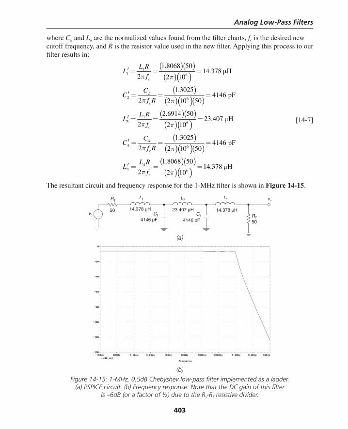
Analog Low-Pass Filters
403
where Cn and Ln are the normalized values found from the fi lter charts, fc is the desired new cutoff frequency, and R is the resistor value used in the new fi lter. Applying this process to our fi lter results in:
( )( )( )( )
( )( )( )( )
( )( )( )( )
( )( )( )( )
( )( )( )( )
11 6
22 6
33 6
44 6
44 6
1.8068 5014.378 H
2 2 10
1.30254146 pF
2 2 10 50
2.6914 5023.407 H
2 2 10
1.30254146 pF
2 2 10 50
1.8068 5014.378 H
2 2 10
c
c
c
c
c
L RL
f
CC
f R
L RL
f
CC
f R
L RL
f
π π
π π
π π
π π
π π
′ = = = μ
′ = = =
′ = = = μ
′ = = =
′ = = = μ
[14-7]
The resultant circuit and frequency response for the 1-MHz fi lter is shown in Figure 14-15.
14.378 µHC4C2
RSL1 L3
vi
voL5
50RT
50 14.378 µH 23.407 µH
4146 pF 4146 pF
+−
(a)
(b)
Figure 14-15: 1-MHz, 0.5dB Chebyshev low-pass fi lter implemented as a ladder. (a) PSPICE circuit. (b) Frequency response. Note that the DC gain of this fi lter
is –6dB (or a factor of ½) due to the Rs-RT resistive divider.
Thompson Book.indb 403 3/20/2006 11:37:09 AM
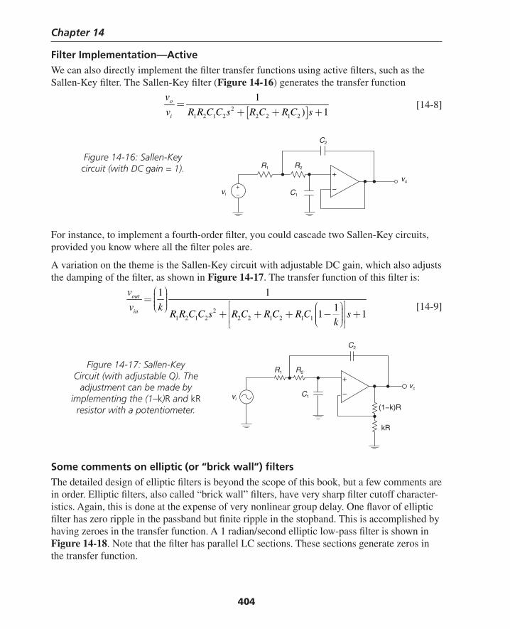
Chapter 14
404
Filter Implementation—ActiveWe can also directly implement the fi lter transfer functions using active fi lters, such as the Sallen-Key fi lter. The Sallen-Key fi lter (Figure 14-16) generates the transfer function
[ ]2
1 2 1 2 2 2 1 2
1
) 1o
i
v
v R R C C s R C R C s=
+ + + [14-8]
For instance, to implement a fourth-order fi lter, you could cascade two Sallen-Key circuits, provided you know where all the fi lter poles are.
A variation on the theme is the Sallen-Key circuit with adjustable DC gain, which also adjusts the damping of the fi lter, as shown in Figure 14-17. The transfer function of this fi lter is:
21 2 1 2 2 2 1 2 1 1
1 1
11 1
out
in
v
v kR R C C s R C R C R C s
k
⎛ ⎞⎟⎜= ⎟⎜ ⎟⎜ ⎡ ⎤⎛ ⎞⎝ ⎠ ⎟⎜⎢ ⎥+ + + − +⎟⎜ ⎟⎜⎢ ⎥⎝ ⎠⎣ ⎦
[14-9]
C1vi
vo
+
−
C2
R2R1
+−
Figure 14-16: Sallen-Key circuit (with DC gain = 1).
Some comments on elliptic (or “brick wall”) fi ltersThe detailed design of elliptic fi lters is beyond the scope of this book, but a few comments are in order. Elliptic fi lters, also called “brick wall” fi lters, have very sharp fi lter cutoff character-istics. Again, this is done at the expense of very nonlinear group delay. One fl avor of elliptic fi lter has zero ripple in the passband but fi nite ripple in the stopband. This is accomplished by having zeroes in the transfer function. A 1 radian/second elliptic low-pass fi lter is shown in Figure 14-18. Note that the fi lter has parallel LC sections. These sections generate zeros in the transfer function.
C1vi
vo
C2
R2R1
+
−
(1−k)R
kR
Figure 14-17: Sallen-Key Circuit (with adjustable Q). The
adjustment can be made by implementing the (1–k)R and kR
resistor with a potentiometer.
Thompson Book.indb 404 3/20/2006 11:37:10 AM
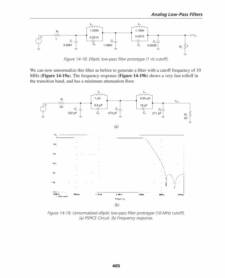
Analog Low-Pass Filters
405
Figure 14-18: Elliptic low-pass fi lter prototype (1 r/s cutoff).
We can now unnormalize this fi lter as before to generate a fi lter with a cutoff frequency of 10 MHz (Figure 14-19a). The frequency response (Figure 14-19b) shows a very fast rolloff in the transition band, and has a minimum attenuation fl oor.
R1
1
1.2560
0.0214
1.1994
0.0575
L2 L4
v1
C1C2
C3
C4
C5
0.6981 1.4860 0.6638
vout
1R2
+−
(a)
R1
50
1 µH
6.8 pF
0.95 µH
18 pF
L2 L4
v1
C1 C3
C4
C5
222 pF 473 pF 211 pF
vout
R2
50
+−
C2
(b)
Figure 14-19: Unnormalized elliptic low-pass fi lter prototype (10-MHz cutoff). (a) PSPICE Circuit. (b) Frequency response.
Thompson Book.indb 405 3/20/2006 11:37:10 AM
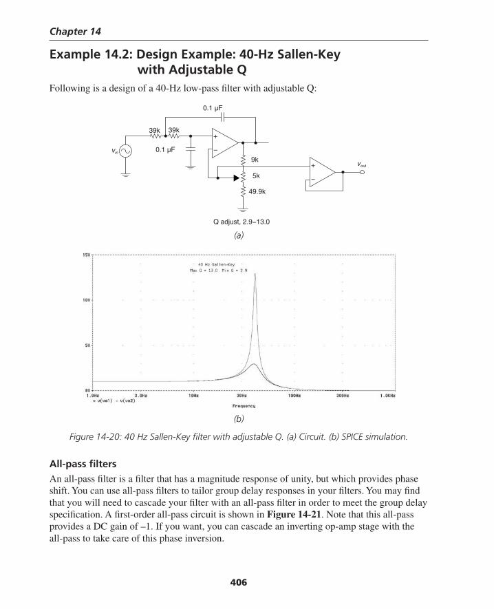
Chapter 14
406
Example 14.2: Design Example: 40-Hz Sallen-Key with Adjustable QFollowing is a design of a 40-Hz low-pass fi lter with adjustable Q:
(a)
vin
vout+
−
+
−
Q adjust, 2.9−13.0
9k
5k
49.9k
39k 39k
0.1 µF
0.1 µF
(b)
Figure 14-20: 40 Hz Sallen-Key fi lter with adjustable Q. (a) Circuit. (b) SPICE simulation.
All-pass fi ltersAn all-pass fi lter is a fi lter that has a magnitude response of unity, but which provides phase shift. You can use all-pass fi lters to tailor group delay responses in your fi lters. You may fi nd that you will need to cascade your fi lter with an all-pass fi lter in order to meet the group delay specifi cation. A fi rst-order all-pass circuit is shown in Figure 14-21. Note that this all-pass provides a DC gain of –1. If you want, you can cascade an inverting op-amp stage with the all-pass to take care of this phase inversion.
Thompson Book.indb 406 3/20/2006 11:37:11 AM
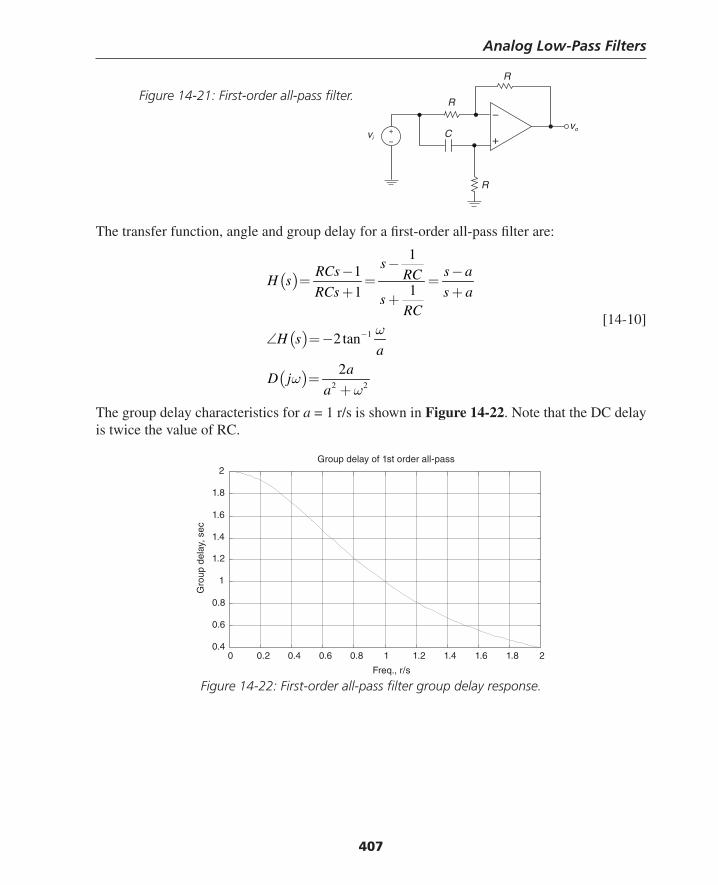
Analog Low-Pass Filters
407
The transfer function, angle and group delay for a fi rst-order all-pass fi lter are:
( )
( )
( )
1
2 2
11
11
2 tan
2
sRCs s aRCH sRCs s as
RC
H sa
aD j
a
ω
ωω
−
−− −= = =
+ ++
∠ = −
=+
[14-10]
The group delay characteristics for a = 1 r/s is shown in Figure 14-22. Note that the DC delay is twice the value of RC.
vi
vo
+
−
R
R
R
C+−
Figure 14-21: First-order all-pass fi lter.
Figure 14-22: First-order all-pass fi lter group delay response.
0 0.2 0.4 0.6 0.8 1 1.2 1.4 1.6 1.8 20.4
0.6
0.8
1
1.2
1.4
1.6
1.8
2
Freq., r/s
Gro
up d
elay
, sec
Group delay of 1st order all-pass
Thompson Book.indb 407 3/20/2006 11:37:12 AM

Chapter 14
408
Example 14.3: Design case study: 1-MHz low-pass fi lterIn this case study, we’ll design and simulate an analog low-pass fi lter meeting the following specifi cations (Table 14-12):
Table 14-12: Design case study specifi cation.
Filter type Low-passNominal –3dB bandwidth 1 MHzPassband gain 0dB nominal, within 0.25dB of nominal up to 750 kHzAttenuation > 50dB at 2.5 MHz
Group delay responseGroup delay variation from the DC value less than 1000 nanoseconds up to 1 MHz
This design could be implemented with either a ladder fi lter with passive elements (resistors, inductors and capacitor) or a cascade of Sallen-Key active second-order sections. If you at-tempt to use a Bessel fi lter, the fi lter order will be quite high. If you look at elliptic fi lters the group delay specifi cation may be very diffi cult to meet.
In this design ωs/ωc = 2.5 and minimum attenuation at ωs is –50dB. A Bessel fi lter was not implemented due to the high fi lter order required. In order to meet the specifi cation for –50dB gain at a normalized frequency of 2.5, a Bessel fi lter of order N > 10 would be needed. A sixth-order Butterworth fi lter would almost make the specifi cation, since
10 12
120 log 47.8dB
1 2.5
⎛ ⎞⎟⎜ ⎟⎜ = −⎟⎜ ⎟⎜ ⎟+⎝ ⎠
So, if we use a Butterworth, we’ll need at least N = 7. The advantage of the Butterworth is that there is no magnitude ripple in the passband.
Another alternative will be to try a Chebyshev design with N = 7 or less and some passband ripple. From our previous work on the Chebyshev fi lter, it looks like an N = 6 Chebyshev with 0.1dB ripple in the passband will meet the specifi cation. An N = 5 Chebyshev with 0.25dB passband ripple barely misses the attenuation spec. So, let’s go with the N = 6, 0.1dB Cheby-shev design (Figure 14-23).
0 0.5 1 1.5 2 2.5 3 3.5 4−100−80−60−40−20
0
dB
Chebyshev example, overall response, filter order N = 6
0 0.1 0.2 0.3 0.4 0.5 0.6 0.7 0.8 0.9 1−0.1
−0.05
0 Chebyshev example, passband response
dB
Figure 14-23: Chebyshev design, N = 6, 0.1dB passband ripple.
Thompson Book.indb 408 3/20/2006 11:37:12 AM
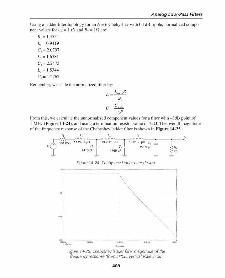
Analog Low-Pass Filters
409
Using a ladder fi lter topology for an N = 6 Chebyshev with 0.1dB ripple, normalized compo-nent values for ωc = 1 r/s and RT = 1Ω are:
Rs = 1.3554
L1 = 0.9419
C2 = 2.0797
L3 = 1.6581
C4 = 2.2473
L5 = 1.5344
C6 = 1.2767
Remember, we scale the normalized fi lter by:
norm
c
norm
c
L RL
CC
R
ω
ω
=
=
From this, we calculate the unnormalized component values for a fi lter with –3dB point of 1 MHz (Figure 14-24), and using a termination resistor value of 75Ω. The overall magnitude of the frequency response of the Chebyshev ladder fi lter is shown in Figure 14-25.
18.3155 µHC4C2
RSL1 L3
vi
voL5
75RT
11.2431 µH 19.7921 µH
4413 pF 4769 pF
+−
C6
2709 pF101.655
Figure 14-24: Chebyshev ladder fi lter design.
Figure 14-25: Chebyshev ladder fi lter magnitude of the frequency response (from SPICE).Vertical scale in dB.
Thompson Book.indb 409 3/20/2006 11:37:13 AM
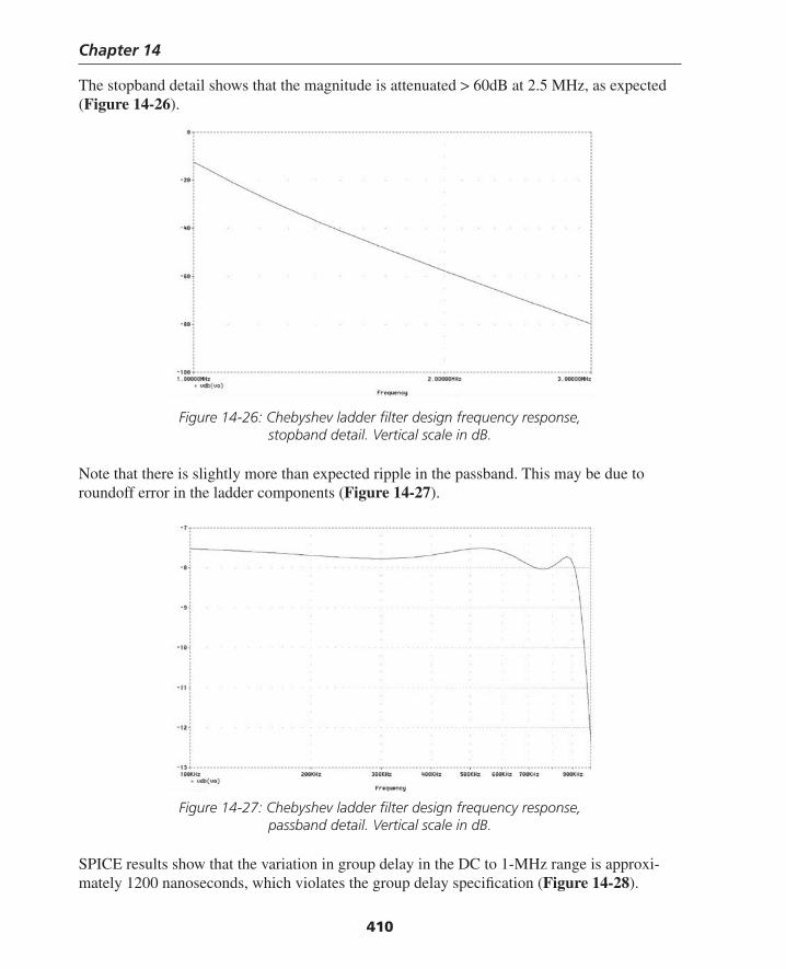
Chapter 14
410
The stopband detail shows that the magnitude is attenuated > 60dB at 2.5 MHz, as expected (Figure 14-26).
Figure 14-26: Chebyshev ladder fi lter design frequency response, stopband detail. Vertical scale in dB.
Note that there is slightly more than expected ripple in the passband. This may be due to roundoff error in the ladder components (Figure 14-27).
Figure 14-27: Chebyshev ladder fi lter design frequency response, passband detail. Vertical scale in dB.
SPICE results show that the variation in group delay in the DC to 1-MHz range is approxi-mately 1200 nanoseconds, which violates the group delay specifi cation (Figure 14-28).
Thompson Book.indb 410 3/20/2006 11:37:14 AM
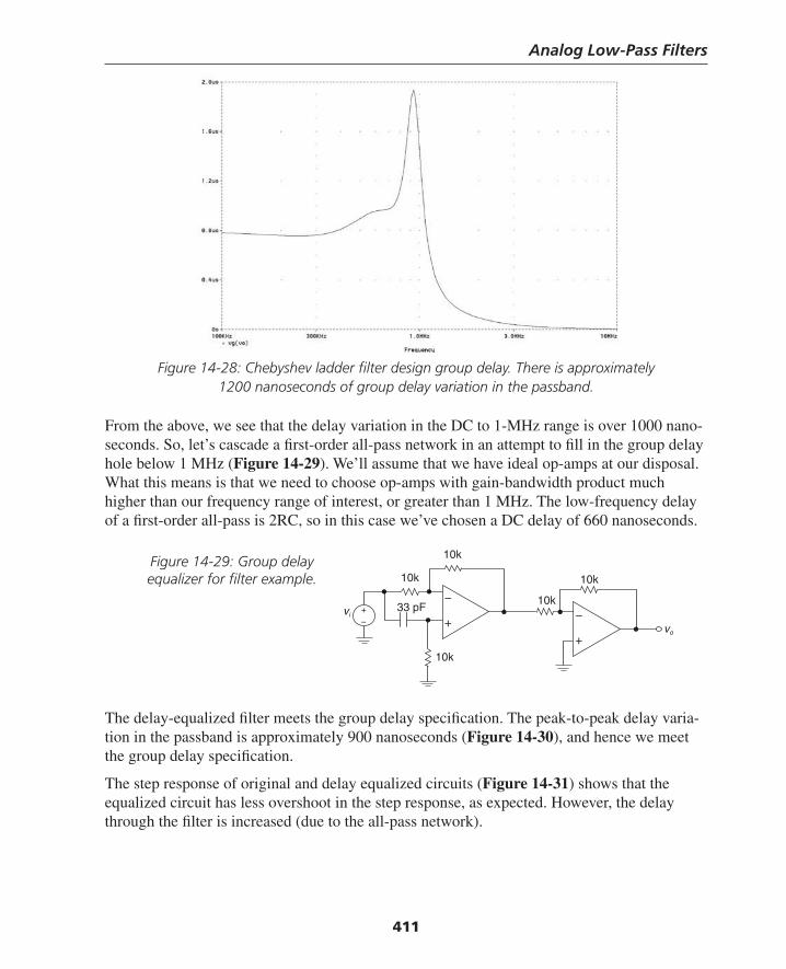
Analog Low-Pass Filters
411
Figure 14-28: Chebyshev ladder fi lter design group delay. There is approximately 1200 nanoseconds of group delay variation in the passband.
From the above, we see that the delay variation in the DC to 1-MHz range is over 1000 nano-seconds. So, let’s cascade a fi rst-order all-pass network in an attempt to fi ll in the group delay hole below 1 MHz (Figure 14-29). We’ll assume that we have ideal op-amps at our disposal. What this means is that we need to choose op-amps with gain-bandwidth product much higher than our frequency range of interest, or greater than 1 MHz. The low-frequency delay of a fi rst-order all-pass is 2RC, so in this case we’ve chosen a DC delay of 660 nanoseconds.
The delay-equalized fi lter meets the group delay specifi cation. The peak-to-peak delay varia-tion in the passband is approximately 900 nanoseconds (Figure 14-30), and hence we meet the group delay specifi cation.
The step response of original and delay equalized circuits (Figure 14-31) shows that the equalized circuit has less overshoot in the step response, as expected. However, the delay through the fi lter is increased (due to the all-pass network).
vi
vo+
−+
−
10k
10k
10k
10k
33 pF
10k
+−
Figure 14-29: Group delay equalizer for fi lter example.
Thompson Book.indb 411 3/20/2006 11:37:15 AM
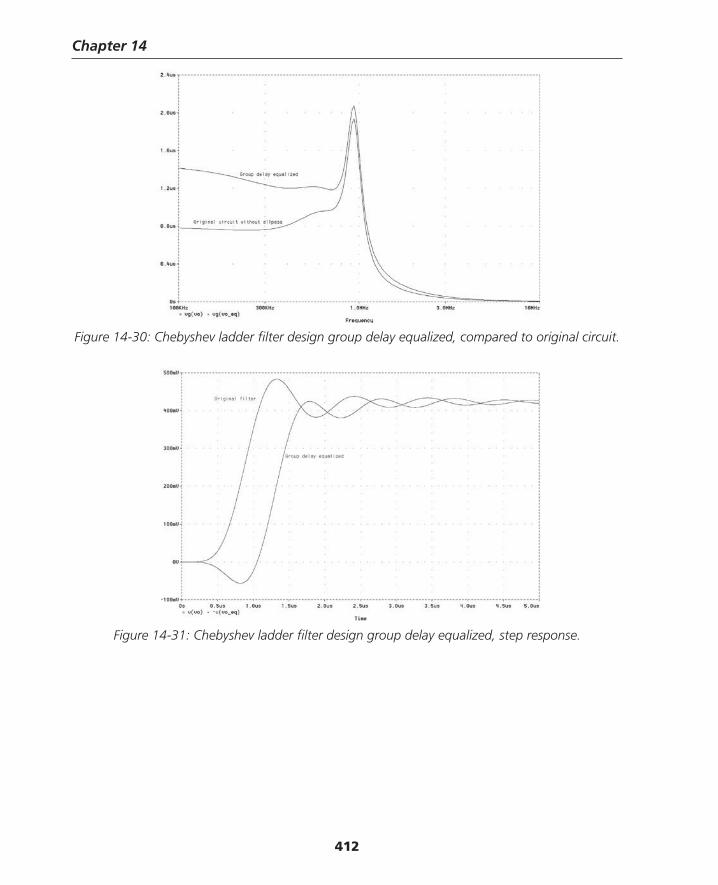
Chapter 14
412
Figure 14-30: Chebyshev ladder fi lter design group delay equalized, compared to original circuit.
Figure 14-31: Chebyshev ladder fi lter design group delay equalized, step response.
Thompson Book.indb 412 3/20/2006 11:37:16 AM
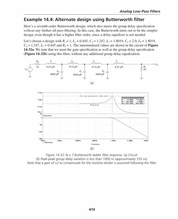
Analog Low-Pass Filters
413
Example 14.4: Alternate design using Butterworth fi lterHere’s a seventh-order Butterworth design, which also meets the group delay specifi cation without any further all-pass fi ltering. In this case, the Butterworth turns out to be the simpler design, even though it has a higher fi lter order, since a delay equalizer is not needed.
Let’s choose a design with Rs = 1, L1 = 0.445, C2 = 1.247, L3 = 1.8019, C4 = 2.0, L5 = 1.8019, C6 = 1.247, L7 = 0.445 and RT = 1. The unnormalized values are shown in the circuit of Figure 14-32a. We note that we meet the gain specifi cation as well as the group delay specifi cation (Figure 14-32b) using this fi lter, without any additional group delay equalization.
(a)
21.5 µH 5.31 µH
C4C2
RSL1 L3
vin
vout
L5 L7
75RT5.31 µH 21.5 µH
2650 pF 4240 pF
+− C6
2650 pF
75
(b)
Figure 14-32: N = 7 Butterworth ladder fi lter response. (a) Circuit. (b) Peak-peak group delay variation is less than 1000 ns (approximately 535 ns).
Note that a gain of +2 to compensate for the resistive divider is assumed following the fi lter.
Thompson Book.indb 413 3/20/2006 11:37:17 AM
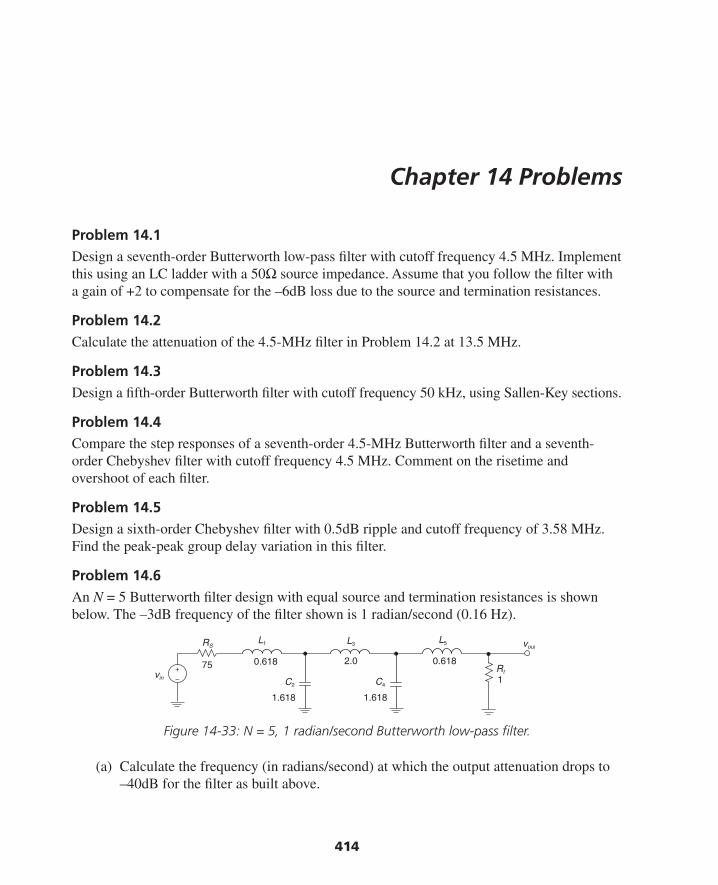
414
Chapter 14 Problems
Problem 14.1Design a seventh-order Butterworth low-pass fi lter with cutoff frequency 4.5 MHz. Implement this using an LC ladder with a 50Ω source impedance. Assume that you follow the fi lter with a gain of +2 to compensate for the –6dB loss due to the source and termination resistances.
Problem 14.2Calculate the attenuation of the 4.5-MHz fi lter in Problem 14.2 at 13.5 MHz.
Problem 14.3Design a fi fth-order Butterworth fi lter with cutoff frequency 50 kHz, using Sallen-Key sections.
Problem 14.4Compare the step responses of a seventh-order 4.5-MHz Butterworth fi lter and a seventh- order Chebyshev fi lter with cutoff frequency 4.5 MHz. Comment on the risetime and overshoot of each fi lter.
Problem 14.5Design a sixth-order Chebyshev fi lter with 0.5dB ripple and cutoff frequency of 3.58 MHz. Find the peak-peak group delay variation in this fi lter.
Problem 14.6An N = 5 Butterworth fi lter design with equal source and termination resistances is shown below. The –3dB frequency of the fi lter shown is 1 radian/second (0.16 Hz).
Figure 14-33: N = 5, 1 radian/second Butterworth low-pass fi lter.
(a) Calculate the frequency (in radians/second) at which the output attenuation drops to –40dB for the fi lter as built above.
0.618
C4C2
RSL1 L3
vin
L5
1Rt
0.618 2.0
1.618 1.618
+−
75
vout
Thompson Book.indb 414 3/20/2006 11:37:17 AM

Analog Low-Pass Filters
415
(b) Now, assume a source and termination resistance of 75Ω. You now need a fi lter with a –3dB cutoff at 10 MHz (not radians/sec!). Find the unnormalized Butterworth values and sketch the circuit.
(c) Sketch the group delay vs. frequency of the 10-MHz fi lter. In your sketch, include at least the following data points: DC, 5 MHz, 10 MHz and 15 MHz. Indicate the frequency at which the group delay peaks.
Problem 14.7A low-pass fi lter prototype with –3dB cutoff frequency has a group delay at DC of 1 second. The prototype fi lter is then transformed and a fi lter with the same type and order is created, but now with a –3dB cutoff frequency of 4.5 MHz. What is the group delay at DC of the new fi lter?
Thompson Book.indb 415 3/20/2006 11:37:18 AM
Chapter 14
416
ReferencesBalch, Brent, “A Simple Technique Boosts Performance of Active Filters,” EDN, November
10, 1988, pp. 277–286.Blinchikoff, H., and Zverev, A., Filtering in the Time and Frequency Domains, John Wiley,
1976.Burton, L. T., and Treleaven, D., “Active Filter Design Using Generalized Impedance Con-
verters,” EDN, February 5, 1973, pp. 68–75.Chambers, William, “Know Your Options and Requirements when Designing Filters,” EDN,
August 5, 1991, pp. 129–138.Corral, C., “Designing elliptic fi lters with maximum selectivity,” EDN, May 25, 2000, pp.
101–109.Corrington, Murlan S., “Transient Response of Filters,” RCA Review, September 1949, vol.
10, no. 3, pp. 397–429.Downs, Rick, “Vintage Filter Scheme Yields Low Distortion in New Audio Designs,” EDN,
November 7, 1991, pp. 267–272.Steer, Robert, Jr., “Antialiasing Filters Reduce Errors in A/D Converters,” EDN, March 30,
1989, pp. 171–186.Tow, J., “A Step-by-Step Active-Filter Design,” IEEE Spectrum, December 1969, pp. 64–68.Williams, A., and Taylor, F., Electronic Filter Design Handbook, McGraw-Hill, 1988.Yager, Charles, and Laber, Carlos, “Create a High-Frequency Complex Filter,” Electronic
Design, April 13, 1989, pp. 123–127.Zverev, Anatol, Handbook of Filter Synthesis, John Wiley, 1967.
Thompson Book.indb 416 3/20/2006 11:37:18 AM
417
C H A P T E R 15Review of Passive Components and
a Case Study in PC Board Layout
ResistorsAt fi rst blush, a resistor is a resistor is a resistor. However, we’ll now delve into some of the subtleties of these devices. The impedance of an ideal resistor is not dependent on operating frequency,1 and is:
,resistor idealZ R= [15-1]
A real-world resistor (Figure 15-1) includes a parasitic inductance due to the geometry of the lead length, and a parasitic capacitance across the resistor. The impedance of the resistor, including these parasitic elements, is:2
( ), 2 2
1
1 1resistor real
LR s
Ls R RZ s
LCs RCs LCs RCs
⎛ ⎞⎟⎜ + ⎟⎜ ⎟⎜⎝ ⎠+= =
+ + + +
[15-2]
We can put this in “jω” form by making the substitution s = jω resulting in:
( )( ), 21
resistor real
j L RZ j
LC j RC
ωω
ω ω+
=− +
[15-3]
In This Chapter
Some of the subtleties of passive components including construction techniques of these devices and parasitic effects are considered. We’ll cover some details about resistors, capacitors and inductors. Then, we’ll use what we’ve learned in an illustrative discussion of PC board layout issues.
1 Another way to look at this is that the current in an ideal resistor and a voltage across this ideal resistor are in phase.
2 One way to sanity-check this result is to consider the limit as L 0 and C 0; we want the impedance to be exactly R and this is indeed the case.
Thompson Book.indb 417 3/20/2006 11:37:18 AM
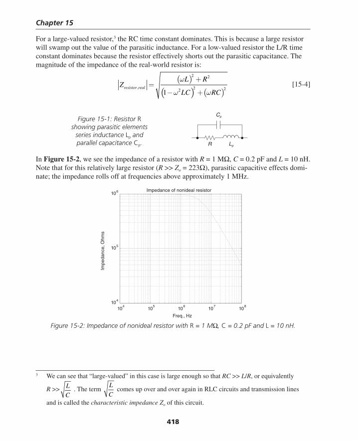
Chapter 15
418
For a large-valued resistor,3 the RC time constant dominates. This is because a large resistor will swamp out the value of the parasitic inductance. For a low-valued resistor the L/R time constant dominates because the resistor effectively shorts out the parasitic capacitance. The magnitude of the impedance of the real-world resistor is:
( )
( ) ( )
2 2
, 2 221resistor real
L RZ
LC RC
ω
ω ω
+=
− + [15-4]
3 We can see that “large-valued” in this case is large enough so that RC >> L/R, or equivalently
R >> L
C . The term
L
C comes up over and over again in RLC circuits and transmission lines
and is called the characteristic impedance Zo of this circuit.
Figure 15-1: Resistor R showing parasitic elements
series inductance Lp and parallel capacitance Cp. R Lp
Cp
In Figure 15-2, we see the impedance of a resistor with R = 1 MΩ, C = 0.2 pF and L = 10 nH. Note that for this relatively large resistor (R >> Zo = 223Ω), parasitic capacitive effects domi-nate; the impedance rolls off at frequencies above approximately 1 MHz.
Figure 15-2: Impedance of nonideal resistor with R = 1 MΩ, C = 0.2 pF and L = 10 nH.
104
105
106
107
108
104
105
106 Impedance of nonideal resistor
Freq., Hz
Impe
danc
e, O
hms
Thompson Book.indb 418 3/20/2006 11:37:18 AM

Review of Passive Components and a Case Study in PC Board Layout
419
In Figure 15-3, we see the impedance of a low-valued resistor with R = 10Ω, C = 0.2 pF and L = 10 nH. Note that parasitic inductive effects dominate; the impedance increases at frequen-cies above approximately 10 Mrad/sec.
105 106 107 108 109101
101.1
Impedance of ideal vs. nonideal resistor
Freq., Hz
Impe
danc
e, O
hms
4 A very rough rule of thumb for the inductance of component leads above a ground plane is 10 nanohenries per centimeter of lead length. So, it behooves you to keep lead lengths short if you want to minimize parasitic inductance. Of course, you can test your resistor using an impedance analyzer (such as the Hewlett Packard HP4192) and extract the parameters for your device.
Figure 15-3: Impedance of nonideal resistor R = 10Ω, C = 0.2 pF and L = 10 nH.
It’s diffi cult to quantify exactly the values of parasitic elements, but in standard through-hole resistors you might expect fractions of a picofarad of parasitic capacitance, and a few nano-henries of parasitic inductance.4 You need to consider such parasitics as series inductance and parallel resistance in high-frequency circuits.
Comments on Surface-Mount ResistorsYou can miniaturize your circuit and reduce somewhat the effects of parasitic inductance by using surface-mount resistors. Surface-mount resistors come in a variety of sizes, ranging from “0201” size, through “0402” size and all the way up to “2512” size. The resistor size numbers indicate the length and width of the resistor. For instance, an 0805 resistor is 0.08" in length and 0.05" in width.
There is a trade-off to be made with regard to resistor size and wattage and working voltage rating, as shown in Table 15-1. For instance, a longer resistor will have a higher working voltage rating, due to a higher voltage breakdown.
Thompson Book.indb 419 3/20/2006 11:37:19 AM
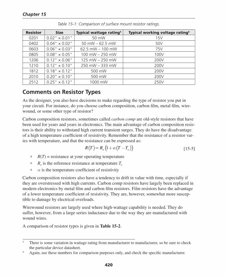
Chapter 15
420
Table 15-1: Comparison of surface mount resistor ratings.
Resistor Size Typical wattage rating5 Typical working voltage rating6
0201 0.02" × 0.01" 50 mW 15V0402 0.04" × 0.02" 50 mW – 62.5 mW 50V0603 0.06" × 0.03" 62.5 mW – 100 mW 75V0805 0.08" × 0.05" 100 mW – 250 mW 100V1206 0.12" × 0.06" 125 mW – 250 mW 200V1210 0.12" × 0.10" 250 mW – 333 mW 200V1812 0.18" × 0.12" 500 mW 200V2010 0.20" × 0.10" 500 mW 200V2512 0.25" × 0.12" 1000 mW 250V
Comments on Resistor TypesAs the designer, you also have decisions to make regarding the type of resistor you put in your circuit. For instance, do you choose carbon composition, carbon fi lm, metal fi lm, wire-wound, or some other type of resistor?
Carbon composition resistors, sometimes called carbon comp are old-style resistors that have been used for years and years in electronics. The main advantage of carbon composition resis-tors is their ability to withstand high current transient surges. They do have the disadvantage of a high temperature coeffi cient of resistivity. Remember that the resistance of a resistor var-ies with temperature, and that the resistance can be expressed as:
( ) ( )( )1o oR T R T Tα= + − [15-5]
• R(T) = resistance at your operating temperature
• Ro is the reference resistance at temperature To
• α is the temperature coeffi cient of resistivity
Carbon composition resistors also have a tendency to drift in value with time, especially if they are overstressed with high currents. Carbon comp resistors have largely been replaced in modern electronics by metal fi lm and carbon fi lm resistors. Film resistors have the advantage of a lower temperature coeffi cient of resistivity. They are, however, somewhat more suscep-tible to damage by electrical overloads.
Wirewound resistors are largely used where high-wattage capability is needed. They do suffer, however, from a large series inductance due to the way they are manufactured with wound wires.
A comparison of resistor types is given in Table 15-2.
5 There is some variation in wattage rating from manufacturer to manufacturer, so be sure to check the particular device datasheet.
6 Again, use these numbers for comparison purposes only, and check the specifi c manufacturer.
Thompson Book.indb 420 3/20/2006 11:37:20 AM
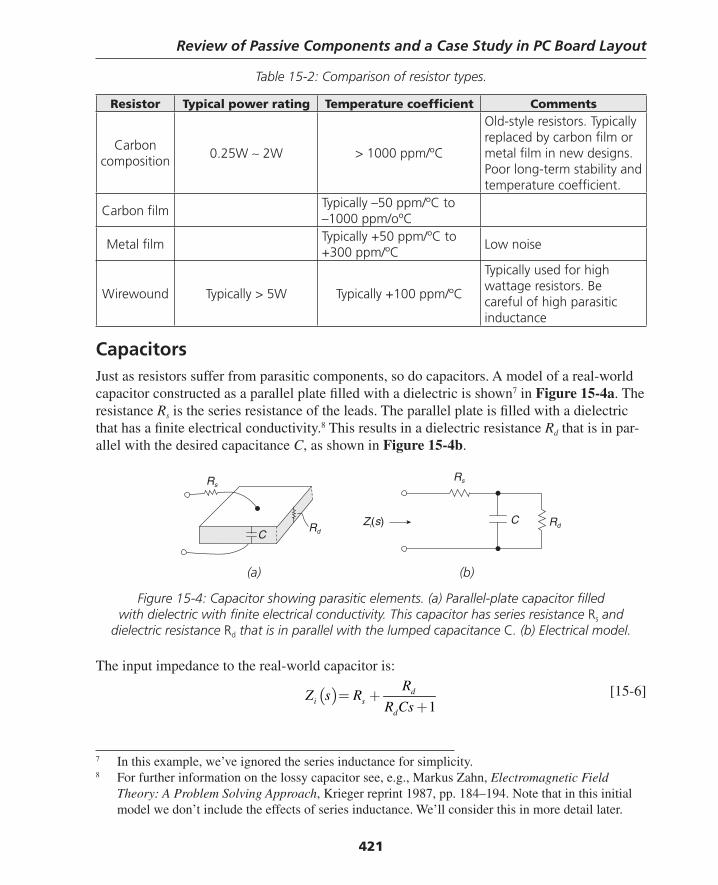
Review of Passive Components and a Case Study in PC Board Layout
421
Table 15-2: Comparison of resistor types.
Resistor Typical power rating Temperature coeffi cient Comments
Carbon composition
0.25W ∼ 2W > 1000 ppm/ºC
Old-style resistors. Typically replaced by carbon fi lm or metal fi lm in new designs. Poor long-term stability and temperature coeffi cient.
Carbon fi lmTypically –50 ppm/ºC to –1000 ppm/oºC
Metal fi lmTypically +50 ppm/ºC to +300 ppm/ºC
Low noise
Wirewound Typically > 5W Typically +100 ppm/ºC
Typically used for high wattage resistors. Be careful of high parasitic inductance
CapacitorsJust as resistors suffer from parasitic components, so do capacitors. A model of a real-world capacitor constructed as a parallel plate fi lled with a dielectric is shown7 in Figure 15-4a. The resistance Rs is the series resistance of the leads. The parallel plate is fi lled with a dielectric that has a fi nite electrical conductivity.8 This results in a dielectric resistance Rd that is in par-allel with the desired capacitance C, as shown in Figure 15-4b.
7 In this example, we’ve ignored the series inductance for simplicity.8 For further information on the lossy capacitor see, e.g., Markus Zahn, Electromagnetic Field
Theory: A Problem Solving Approach, Krieger reprint 1987, pp. 184–194. Note that in this initial model we don’t include the effects of series inductance. We’ll consider this in more detail later.
(a) (b)
Figure 15-4: Capacitor showing parasitic elements. (a) Parallel-plate capacitor fi lled with dielectric with fi nite electrical conductivity. This capacitor has series resistance Rs and
dielectric resistance Rd that is in parallel with the lumped capacitance C. (b) Electrical model.
The input impedance to the real-world capacitor is:
( )1
di s
d
RZ s R
R Cs= +
+ [15-6]
Rs
C RdZi(s)RdC
Rs
Thompson Book.indb 421 3/20/2006 11:37:20 AM
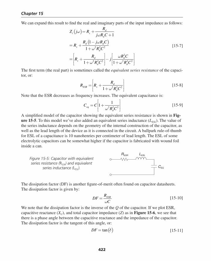
Chapter 15
422
We can expand this result to fi nd the real and imaginary parts of the input impedance as follows:
( )
( )2 2 2
2
2 2 2 2 2 2
1
1
1
1 1
di s
d
d ds
d
d ds
d d
RZ j R
j R C
R j R CR
R C
R R CR j
R C R C
ωω
ω
ω
ωω ω
= ++
−= +
+
⎡ ⎤ ⎡ ⎤⎢ ⎥ ⎢ ⎥= + −⎢ ⎥ ⎢ ⎥+ +⎣ ⎦ ⎣ ⎦
[15-7]
The fi rst term (the real part) is sometimes called the equivalent series resistance of the capaci-tor, or:
2 2 21
dESR s
d
RR R
R Cω
⎡ ⎤⎢ ⎥= +⎢ ⎥+⎣ ⎦
[15-8]
Note that the ESR decreases as frequency increases. The equivalent capacitance is:
2 2 2
11eq
d
C CR Cω
⎡ ⎤⎢ ⎥= +⎢ ⎥⎣ ⎦
[15-9]
A simplifi ed model of the capacitor showing the equivalent series resistance is shown in Fig-ure 15-5. To this model we’ve also added an equivalent series inductance (LESL). The value of the series inductance depends on the geometry of the internal construction of the capacitor, as well as the lead length of the device as it is connected in the circuit. A ballpark rule-of-thumb for ESL of a capacitance is 10 nanohenries per centimeter of lead length. The ESL of some electrolytic capacitors can be somewhat higher if the capacitor is fabricated with wound foil inside a can.
The dissipation factor (DF) is another fi gure-of-merit often found on capacitor datasheets. The dissipation factor is given by:
ESRRDF
Cω= [15-10]
We note that the dissipation factor is the inverse of the Q of the capacitor. If we plot ESR, capacitive reactance (XC), and total capacitor impedance (Z) as in Figure 15-6, we see that there is a phase angle between the capacitive reactance and the impedance of the capacitor. The dissipation factor is the tangent of this angle, or:
( )tanDF δ= [15-11]
CEQ
RESR LESL
Figure 15-5: Capacitor with equivalent series resistance (RESR) and equivalent
series inductance (LESL).
Thompson Book.indb 422 3/20/2006 11:37:20 AM
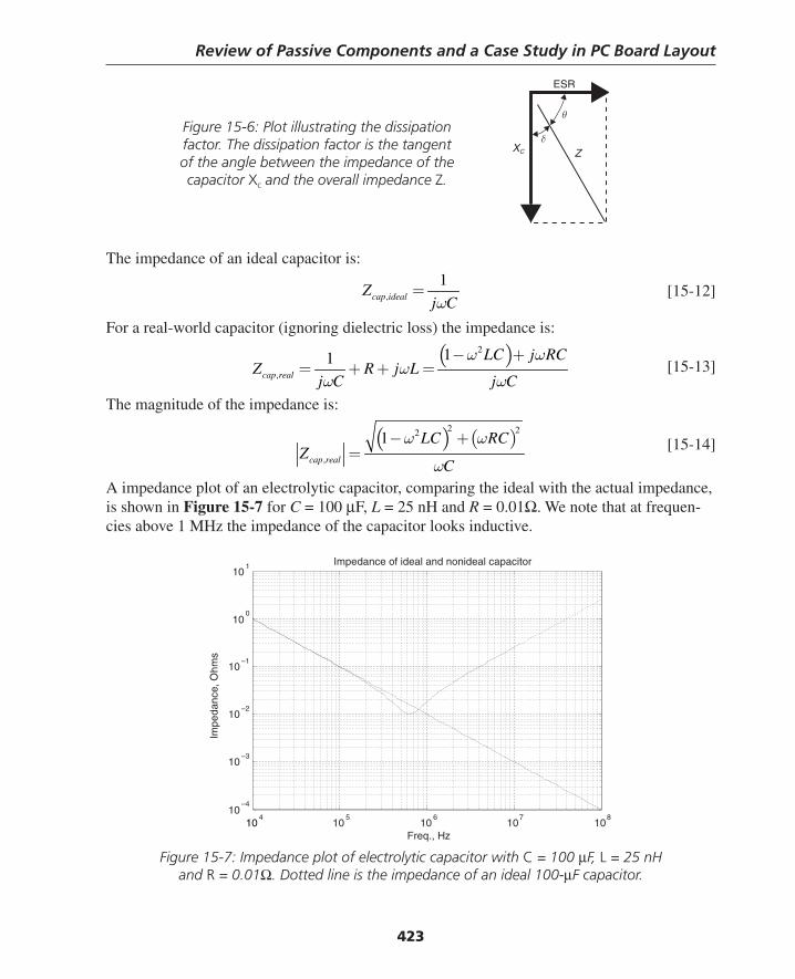
Review of Passive Components and a Case Study in PC Board Layout
423
The impedance of an ideal capacitor is:
,
1cap idealZ
j Cω= [15-12]
For a real-world capacitor (ignoring dielectric loss) the impedance is:
( )2
,
11cap real
LC j RCZ R j L
j C j C
ω ωω
ω ω
− += + + = [15-13]
The magnitude of the impedance is:
( ) ( )2 22
,
1cap real
LC RCZ
C
ω ω
ω
− += [15-14]
A impedance plot of an electrolytic capacitor, comparing the ideal with the actual impedance, is shown in Figure 15-7 for C = 100 μF, L = 25 nH and R = 0.01Ω. We note that at frequen-cies above 1 MHz the impedance of the capacitor looks inductive.
ESR
XC
θ
δZ
Figure 15-6: Plot illustrating the dissipation factor. The dissipation factor is the tangent of the angle between the impedance of the capacitor Xc and the overall impedance Z.
Figure 15-7: Impedance plot of electrolytic capacitor with C = 100 μF, L = 25 nH and R = 0.01Ω. Dotted line is the impedance of an ideal 100-μF capacitor.
104
105
106
107
108
10–4
10–3
10–2
10–1
100
101 Impedance of ideal and nonideal capacitor
Freq., Hz
Impe
danc
e, O
hms
Thompson Book.indb 423 3/20/2006 11:37:21 AM
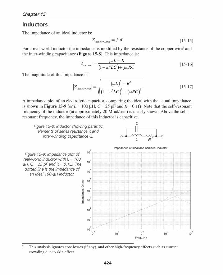
Chapter 15
424
InductorsThe impedance of an ideal inductor is:
,inductor idealZ j Lω= [15-15]
For a real-world inductor the impedance is modifi ed by the resistance of the copper wire9 and the inter-winding capacitance (Figure 15-8). This impedance is:
( ), 21cap real
j L RZ
LC j RC
ωω ω
+=
− + [15-16]
The magnitude of this impedance is:
( )
( ) ( )
2 2
, 2 221inductor real
L RZ
LC RC
ω
ω ω
+=
− + [15-17]
A impedance plot of an electrolytic capacitor, comparing the ideal with the actual impedance, is shown in Figure 15-9 for L = 100 μH, C = 25 pF and R = 0.1Ω. Note that the self-resonant frequency of the inductor (at approximately 20 Mrad/sec.) is clearly shown. Above the self-resonant frequency, the impedance of this inductor is capacitive.
9 This analysis ignores core losses (if any), and other high-frequency effects such as current crowding due to skin effect.
Figure 15-8: Inductor showing parasitic elements of series resistance R and
inter-winding capacitance C.L R
C
Figure 15-9: Impedance plot of real-world inductor with L = 100 μH, C = 25 pF and R = 0.1Ω. The dotted line is the impedance of
an ideal 100-μH inductor.
104
105
106
107
108
100
101
102
103
104
105
106
107
108
Impedance of ideal and nonideal inductor
Freq., Hz
Impe
danc
e, O
hms
Thompson Book.indb 424 3/20/2006 11:37:22 AM

Review of Passive Components and a Case Study in PC Board Layout
425
Discussion of Printed-Circuit Board Layout IssuesPrinted circuit (PC) board layout and routing is a task that is sometimes left to the last minute in a design cycle. Doing a good PC board layout requires attention to many details, including:
• Knowledge of where you want the high frequency, high current, or sensitive circuitry to be.
• Some information on component limitations.
• Information on noise sources.
• Real-world constraints, such as PC board form-factor and location of connectors and mounting holes.
• Other constraints such as PC board design rules mandating minimum trace widths, trace-to-trace spacing, and the like.
Following is a discussion of some of these design issues.
Power supply bypassingThe need for power supply bypassing from integrated circuits arises from the fact that there is no such thing as a perfect, zero-impedance ground. Consider the model of an integrated cir-cuit IC1 in Figure 15-10, the details of which are unimportant for purposes of this discussion. The IC draws DC power from the supply (Vsupply) through wires or ground and power planes. The series inductance and resistance of the interconnection to the supply is shown.
The integrated circuit IC1 draws a fast switching current with a high di/dt (modeled as current source i(t)). The hope in bypassing the IC is that proper selection and placement of the bypass capacitor CB will force transient currents to circulate locally near the integrated circuit and hence voltage transients on the supply lines will be limited. Of course, we want the DC com-ponent of the IC1 current to travel back to the power supply. However, if we send fast current pulses back to the power supply, we will induce voltages on the power supply lines to IC2 and IC3 due to distributed resistance and inductance.
The key to selection and placement of bypass capacitor CB is to choose a capacitor that is suf-fi ciently sized to do the job, and to place it in close proximity to the power and ground pins of IC1. This will minimize the inductance of the bypass path and ensure that the high-frequency switching currents circulate locally near the IC.
CB
+− Vsupply
IC1 IC3IC2
i(t)
Figure 15-10: Model showing integrated circuit drawing current, and its bypass path. CB is the bypass capacitor for IC1.
Thompson Book.indb 425 3/20/2006 11:37:23 AM

Chapter 15
426
One way to reduce the impedance of current return paths is to use a ground plane, discussed in the following section.
Ground planesA ground is a return path for current. It is desirable that this return path should have as low an impedance as possible, to reduce transient-induced voltage drops and electromagnetic emis-sions. In the world of two-layer PC boards, it’s diffi cult to have a dedicated ground plane since you generally want a couple of PC board layers available for routing signals. In multilayer boards, it’s easy to dedicate an unbroken ground plane on an internal PC board layer as ground.
The use of a ground plane helps to reduce the inductance of signal-carrying traces on the PC board. One technique is to have high current and high di/dt traces directly above an unbroken ground plane. You can also make the traces wide if you want to reduce the inductance.
PCB trace widthsPCB traces must be sized appropriately (both in width and thickness, or copper weight10) to carry the current that you need without excessive temperature rise. A rule of thumb is that a 10-mil-wide, 1-ounce PC board trace can carry in excess of 500 mA with a 20°C temperature rise above ambient. An estimate of the current-carrying capability for 20°C temperature rise of PC board traces is shown in Figure 15-11. The fusing current (Figure 15-12) for PC traces is higher.
Table 15-3: PC board copper weight vs. thickness.
Copper weight Copper thickness (inches/mils)½ oz. 0.0007" (0.7 mils)1.0 oz. 0.0014" (1.4 mils)2.0 oz. 0.0028" (2.8 mils)
10 “Copper weight” tells you how thick the PC board trace is. Typical low-power analog boards use ½-ounce or 1-ounce copper. High-power boards may use 2-ounce copper or higher.
Thompson Book.indb 426 3/20/2006 11:37:23 AM

Review of Passive Components and a Case Study in PC Board Layout
427
Figure 15-12: Approximate fusing current of 0.5 oz., 1.0 oz. and 2.0 oz. PCB12 traces.
Figure 15-11: Approximate current-carrying capability of 0.5 oz., 1.0 oz. and 2.0 oz. PCB traces with 20°C temperature rise.11
The upper trace is 2 oz. copper; the lower trace is 0.5 oz. (Note: 1 mil = 0.001")
0 10 20 30 40 50 60 70 80 90 1000
1
2
3
4
5
6
7
8PCB current-carrying capacity vs. PCB trace width for 20C rise
PCB trace width, mils
Ima
x, A
mps
11 From Douglas Brooks, reference at the end of this chapter.12 From Douglas Brooks, “Fusing Current” reference at the end of this chapter
0 20 40 60 80 1000
5
10
15
20
25
30
35
40
45
PCB trace width, mils
Fusing current
Fus
ing
curr
ent,
Am
ps
Thompson Book.indb 427 3/20/2006 11:37:23 AM
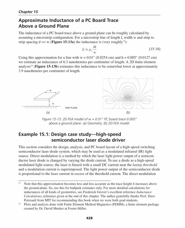
Chapter 15
428
Approximate Inductance of a PC Board Trace Above a Ground PlaneThe inductance of a PC board trace above a ground plane can be roughly calculated by assuming a microstrip confi guration. For a microstrip line of length l, width w and strip to strip spacing d << w (Figure 15-13a) the inductance is (very roughly13):
Llh
wo≈ μ [15-18]
Using this approximation for a line with w = 0.01" (0.0254 cm) and h = 0.005" (0.0127 cm) we estimate an inductance of 6.3 nanohenries per centimeter of length. A 2D fi nite element analysis14 (Figure 15-13b) estimates this inductance to be somewhat lower at approximately 3.9 nanohenries per centimeter of length.
13 Note that this approximation becomes less and less accurate as the trace height h increases above the ground plane. So, use this for ballpark estimates only. For more detailed calculations for inductances of all kinds of geometries, see Frederick Grover’s excellent reference Inductance Calculations, reference given at the end of this chapter. The author gratefully thanks Prof. Dave Perreault from MIT for recommending this book when we were both grad students.
14 Plots and analysis done with Finite Element Method Magnetics (FEMM), a fi nite element package created by Dr. David Meeker at Foster-Miller.
(a) (b)
Figure 15-13: 2D FEA model of w = 0.01" PC board trace 0.005" above a ground plane. (a) Geometry. (b) 2D FEA model.
Example 15.1: Design case study—high-speed semiconductor laser diode driverThis section considers the design, analysis, and PC board layout of a high-speed switching semiconductor laser diode system, which may be used as a modulated infrared (IR) light source. Direct modulation is a method by which the laser light power output of a semicon-ductor laser diode is changed by varying the diode current. To use a diode as a high-speed modulated light source, the laser is biased with a small DC current near the lasing threshold and a modulation current is superimposed. The light power output of the semiconductor diode is proportional to the laser current in excess of the threshold current. The direct modulation
GND PLANE
w
h
Thompson Book.indb 428 3/20/2006 11:37:24 AM
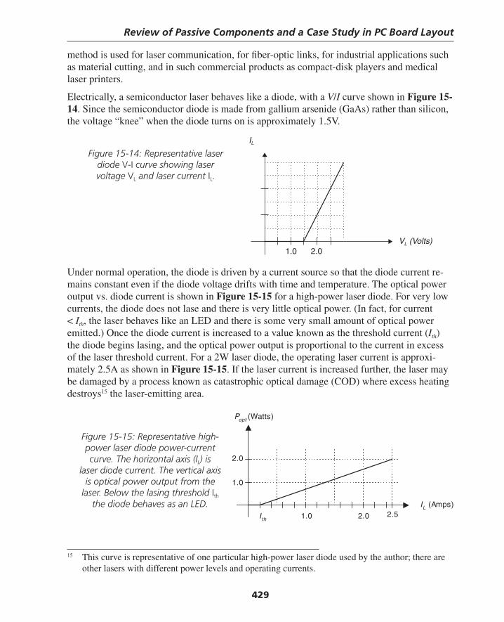
Review of Passive Components and a Case Study in PC Board Layout
429
method is used for laser communication, for fi ber-optic links, for industrial applications such as material cutting, and in such commercial products as compact-disk players and medical laser printers.
Electrically, a semiconductor laser behaves like a diode, with a V/I curve shown in Figure 15-14. Since the semiconductor diode is made from gallium arsenide (GaAs) rather than silicon, the voltage “knee” when the diode turns on is approximately 1.5V.
VL (Volts)
IL
1.0 2.0
Figure 15-14: Representative laser diode V-I curve showing laser voltage VL and laser current IL.
Under normal operation, the diode is driven by a current source so that the diode current re-mains constant even if the diode voltage drifts with time and temperature. The optical power output vs. diode current is shown in Figure 15-15 for a high-power laser diode. For very low currents, the diode does not lase and there is very little optical power. (In fact, for current < Ith, the laser behaves like an LED and there is some very small amount of optical power emitted.) Once the diode current is increased to a value known as the threshold current (Ith) the diode begins lasing, and the optical power output is proportional to the current in excess of the laser threshold current. For a 2W laser diode, the operating laser current is approxi-mately 2.5A as shown in Figure 15-15. If the laser current is increased further, the laser may be damaged by a process known as catastrophic optical damage (COD) where excess heating destroys15 the laser-emitting area.
15 This curve is representative of one particular high-power laser diode used by the author; there are other lasers with different power levels and operating currents.
Figure 15-15: Representative high-power laser diode power-current curve. The horizontal axis (IL) is
laser diode current. The vertical axis is optical power output from the
laser. Below the lasing threshold Ith the diode behaves as an LED. IL (Amps)
Popt (Watts)
1.0
2.0
1.0 2.0 2.5Ith
Thompson Book.indb 429 3/20/2006 11:37:24 AM
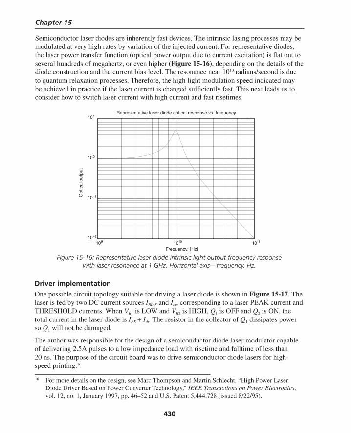
Chapter 15
430
Semiconductor laser diodes are inherently fast devices. The intrinsic lasing processes may be modulated at very high rates by variation of the injected current. For representative diodes, the laser power transfer function (optical power output due to current excitation) is fl at out to several hundreds of megahertz, or even higher (Figure 15-16), depending on the details of the diode construction and the current bias level. The resonance near 1010 radians/second is due to quantum relaxation processes. Therefore, the high light modulation speed indicated may be achieved in practice if the laser current is changed suffi ciently fast. This next leads us to consider how to switch laser current with high current and fast risetimes.
Figure 15-16: Representative laser diode intrinsic light output frequency response with laser resonance at 1 GHz. Horizontal axis—frequency, Hz.
Driver implementationOne possible circuit topology suitable for driving a laser diode is shown in Figure 15-17. The laser is fed by two DC current sources IBIAS and Ith, corresponding to a laser PEAK current and THRESHOLD currents. When VB1 is LOW and VB2 is HIGH, Q1 is OFF and Q2 is ON, the total current in the laser diode is IPK + Ith. The resistor in the collector of Q1 dissipates power so Q1 will not be damaged.
The author was responsible for the design of a semiconductor diode laser modulator capable of delivering 2.5A pulses to a low impedance load with risetime and falltime of less than 20 ns. The purpose of the circuit board was to drive semiconductor diode lasers for high-speed printing.16
109 1010 101110−2
10−1
100
101Representative laser diode optical response vs. frequency
Frequency, [Hz]
Opt
ical
out
put
16 For more details on the design, see Marc Thompson and Martin Schlecht, “High Power Laser Diode Driver Based on Power Converter Technology,” IEEE Transactions on Power Electronics, vol. 12, no. 1, January 1997, pp. 46–52 and U.S. Patent 5,444,728 (issued 8/22/95).
Thompson Book.indb 430 3/20/2006 11:37:25 AM
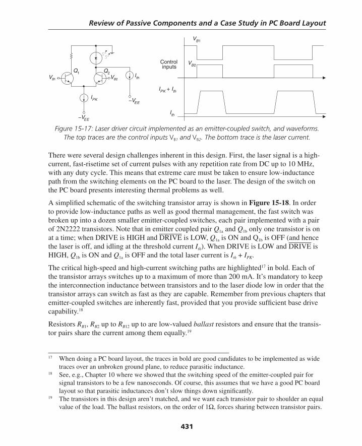
Review of Passive Components and a Case Study in PC Board Layout
431
Figure 15-17: Laser driver circuit implemented as an emitter-coupled switch, and waveforms. The top traces are the control inputs VB1 and VB2. The bottom trace is the laser current.
There were several design challenges inherent in this design. First, the laser signal is a high-current, fast-risetime set of current pulses with any repetition rate from DC up to 10 MHz, with any duty cycle. This means that extreme care must be taken to ensure low-inductance path from the switching elements on the PC board to the laser. The design of the switch on the PC board presents interesting thermal problems as well.
A simplifi ed schematic of the switching transistor array is shown in Figure 15-18. In order to provide low-inductance paths as well as good thermal management, the fast switch was broken up into a dozen smaller emitter-coupled switches, each pair implemented with a pair of 2N2222 transistors. Note that in emitter coupled pair Q1a and Q1b only one transistor is on at a time; when DRIVE is HIGH and DRIVE is LOW, Q1a is ON and Q1b is OFF (and hence the laser is off, and idling at the threshold current Ith). When DRIVE is LOW and DRIVE is HIGH, Q1b is ON and Q1a is OFF and the total laser current is Ith + IPK.
The critical high-speed and high-current switching paths are highlighted17 in bold. Each of the transistor arrays switches up to a maximum of more than 200 mA. It’s mandatory to keep the interconnection inductance between transistors and to the laser diode low in order that the transistor arrays can switch as fast as they are capable. Remember from previous chapters that emitter-coupled switches are inherently fast, provided that you provide suffi cient base drive capability.18
Resistors RB1, RB2 up to RB12 up to are low-valued ballast resistors and ensure that the transis-tor pairs share the current among them equally.19
−VEE
Controlinputs
Ith
IPK
VB1 VB2
Q1 Q2
VB1
VB2
Ith
−VEE
IPK + Ith
17 When doing a PC board layout, the traces in bold are good candidates to be implemented as wide traces over an unbroken ground plane, to reduce parasitic inductance.
18 See, e.g., Chapter 10 where we showed that the switching speed of the emitter-coupled pair for signal transistors to be a few nanoseconds. Of course, this assumes that we have a good PC board layout so that parasitic inductances don’t slow things down signifi cantly.
19 The transistors in this design aren’t matched, and we want each transistor pair to shoulder an equal value of the load. The ballast resistors, on the order of 1Ω, forces sharing between transistor pairs.
Thompson Book.indb 431 3/20/2006 11:37:25 AM
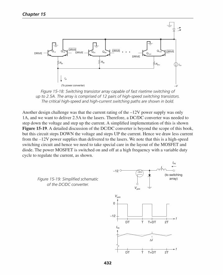
Chapter 15
432
Figure 15-18: Switching transistor array capable of fast risetime switching of up to 2.5A. The array is comprised of 12 pairs of high-speed switching transistors.
The critical high-speed and high-current switching paths are shown in bold.
Another design challenge was that the current rating of the –12V power supply was only 1A, and we want to deliver 2.5A to the lasers. Therefore, a DC/DC converter was needed to step down the voltage and step up the current. A simplifi ed implementation of this is shown Figure 15-19. A detailed discussion of the DC/DC converter is beyond the scope of this book, but this circuit steps DOWN the voltage and steps UP the current. Hence we draw less current from the –12V power supplies than delivered to the lasers. We note that this is a high-speed switching circuit and hence we need to take special care in the layout of the MOSFET and diode. The power MOSFET is switched on and off at a high frequency with a variable duty cycle to regulate the current, as shown.
DRIVE DRIVEDRIVE
DRIVE
DRIVEDRIVEQ1A Q1B
RB1
Q2A Q2B
RB2
Q12A
Q12B
RB12 ITH
Ipk
(To power converter)
• • •
−V
Figure 15-19: Simplifi ed schematic of the DC/DC converter.
IPK
L
Vgate
−12
−12
0
Vgate
(to switchingarray)
t
t
IPK
ΔI
DT T T+DT 2T
DT T T+DT 2T
Thompson Book.indb 432 3/20/2006 11:37:25 AM
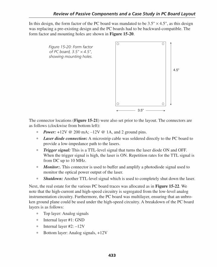
Review of Passive Components and a Case Study in PC Board Layout
433
In this design, the form factor of the PC board was mandated to be 3.5" × 4.5", as this design was replacing a pre-existing design and the PC boards had to be backward-compatible. The form factor and mounting holes are shown in Figure 15-20.
The connector locations (Figure 15-21) were also set prior to the layout. The connectors are as follows (clockwise from bottom left):
• Power: +12V @ 200 mA; –12V @ 1A, and 2 ground pins.
• Laser diode connection: A microstrip cable was soldered directly to the PC board to provide a low-impedance path to the lasers.
• Trigger signal: This is a TTL-level signal that turns the laser diode ON and OFF. When the trigger signal is high, the laser is ON. Repetition rates for the TTL signal is from DC up to 10 MHz.
• Monitor:. This connector is used to buffer and amplify a photodiode signal used to monitor the optical power output of the laser.
• Shutdown: Another TTL-level signal which is used to completely shut down the laser.
Next, the real estate for the various PC board traces was allocated as in Figure 15-22. We note that the high-current and high-speed circuitry is segregated from the low-level analog instrumentation circuitry. Furthermore, the PC board was multilayer, ensuring that an unbro-ken ground plane could be used under the high-speed circuitry. A breakdown of the PC board layers is as follows:
• Top layer: Analog signals
• Internal layer #1: GND
• Internal layer #2: –12V
• Bottom layer: Analog signals, +12V
4.5"
3.5"
Figure 15-20: Form factor of PC board, 3.5" × 4.5", showing mounting holes.
Thompson Book.indb 433 3/20/2006 11:37:26 AM
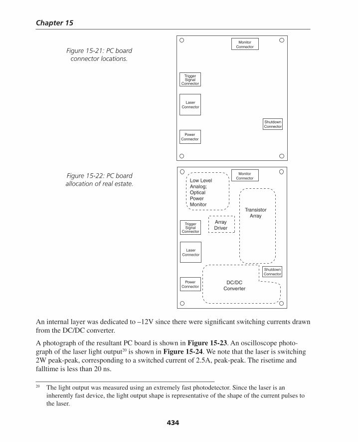
Chapter 15
434
20 The light output was measured using an extremely fast photodetector. Since the laser is an inherently fast device, the light output shape is representative of the shape of the current pulses to the laser.
MonitorConnector
ShutdownConnector
TriggerSignal
Connector
LaserConnector
PowerConnector
ArrayDriver
TransistorArray
Low LevelAnalog;OpticalPowerMonitor
DC/DCConverter
MonitorConnector
ShutdownConnector
TriggerSignal
Connector
LaserConnector
PowerConnector
Figure 15-21: PC board connector locations.
An internal layer was dedicated to –12V since there were signifi cant switching currents drawn from the DC/DC converter.
A photograph of the resultant PC board is shown in Figure 15-23. An oscilloscope photo-graph of the laser light output20 is shown in Figure 15-24. We note that the laser is switching 2W peak-peak, corresponding to a switched current of 2.5A, peak-peak. The risetime and falltime is less than 20 ns.
Figure 15-22: PC board allocation of real estate.
Thompson Book.indb 434 3/20/2006 11:37:26 AM
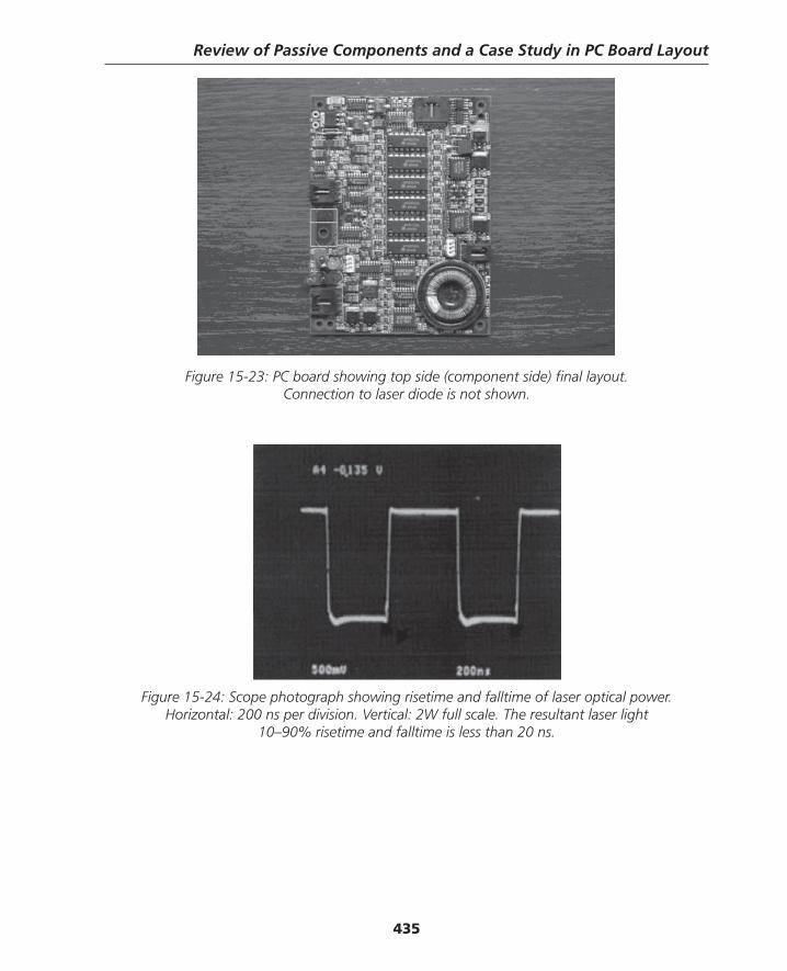
Review of Passive Components and a Case Study in PC Board Layout
435
Figure 15-23: PC board showing top side (component side) fi nal layout. Connection to laser diode is not shown.
Figure 15-24: Scope photograph showing risetime and falltime of laser optical power. Horizontal: 200 ns per division. Vertical: 2W full scale. The resultant laser light
10–90% risetime and falltime is less than 20 ns.
Thompson Book.indb 435 3/20/2006 11:37:26 AM
436
Chapter 15 Problems
Problem 15.1This problem concerns real-world capacitors. Every capacitor has some parasitic elements; that is, there is no such thing as an “ideal capacitor.” For instance, the leads that connect a capacitor to your circuit have a parasitic inductance that is in series with the capacitor. This parasitic series inductance affects how the capacitor operates at high frequency. Also, the capacitor has some internal resistance, also in series with the capacitance, known as the equivalent series resistance (ESR).
(a) Draw the lumped circuit model for the real-world capacitor.
(b) The very approximate inductance of a pair of leads is approximately 1 μH/meter of lead length. For a total lead length of one inch, calculate the self-resonant frequency of the capacitor for C = 1 μF and for C = 1000 μF.
(c) Sketch a Bode (log-log) plot of a capacitor impedance for C = 1000 μF and one inch leads, assuming an equivalent series resistance ESR = 10 mΩ.
(d) Why should you keep lead lengths short ?
Problem 15.2A PC board trace is 0.1" wide, 6" long and is 0.06" above a ground plane. Estimate the trace inductance and trace resistance at room temperature. Assume that the trace is comprised of 1-ounce copper.
Problem 15.3A microstrip line is built with two copper strips each a centimeter wide separated by a 0.005" thick kapton insulator. Estimate the inductance of a 6-inch long piece of microstrip.
Problem 15.4A PC-board mounted inductor has an ideal value of L = 1 μH. However, the measured series resistance of this device is 0.5Ω, and a parallel-resonant frequency of 15 MHz is measured using an impedance analyzer. Generate an appropriate lumped-circuit model for this inductor.
Problem 15.5A fi lm capacitor has an ideal value of 2.2 μF. You initially charge the capacitor to 250V, then disconnect the charging power supply and, using an oscilloscope, discover that the capacitor
Thompson Book.indb 436 3/20/2006 11:37:27 AM
Review of Passive Components and a Case Study in PC Board Layout
437
voltage discharges to 100V in 60 seconds. Find a lumped circuit model of this capacitor, utilizing these fi ndings.
Problem 15.6A MOSFET gate driver IC has a very low impedance, and drives a MOSFET gate where the input impedance may be modeled as a capacitance of 1000 pF. The gate driver is 2 inches away on a PC board, resulting in an approximate series inductance driving the gate from the driver of 50 nH. Draw the circuit model, and fi nd the value of series resistance that you place at the output of the gate driver to achieve critical damping of the gate circuit. Simulate your circuit and fi nd the 10–90% risetime of the gate signal.
ReferencesBartoli, M., Reatti, A., and Kazimierczuk, M., “High-frequency models of ferrite core induc-
tors,” International Conference on Industrial Electronics, Control and Instrumentation, (IECON ’94), September 5–9, 1994, volume 3, pp. 1670–1675.
Brooks, D., “Fusing Currents—When Traces Melt Without a Trace,” available at http://www.ultracad.com, printed in Printed Circuit Design, vol. 15, no. 12, Dec. 1998, pp. 53.
Cao, Y., Groves, R., Huang, X., Zamdmer, N., Plouchart, J., Wachnik, R., King, T., and Hu, C., “Frequency-independent equivalent-circuit model for on-chip spiral inductors,” IEEE Journal of Solid-State Circuits, vol. 38, no. 3, March 2003, pp. 419–426.
Demurie, S. N., and DeMey, G., “Parasitic capacitance effects of planar resistors,” IEEE Transactions on Components, Packaging and Manufacturing Technology, Part A, vol. 12, no. 3, September 1989, pp. 348–351.
Dolan, J. E., and Bolton, H. R., “Capacitor ESR measurement technique,” Eighth IEEE Pulsed Power Conference 1991, June 16–19, 1991, pp. 228–231.
Franco, S., “Polypropylene capacitors for snubber applications,” Proceedings of the Thirty-First IAS Annual Meeting (IAS ’96), October 6–10, 1996, pp. 1337–1342.
Galbraith, J., “Reliable Precision Wirewound Resistor Design,” IRE Transactions on Compo-nents Parts, vol. 3, no. 3, December 1956, pp. 116–119.
Grover, F. W., Inductance Calculations: Working Formulas and Tables, Dover Publications, Inc., New York, 1946.
Jutty, M. K., Swaminathan, V., and Kazimierczuk, M. K., “Frequency characteristics of ferrite core inductors,” Proceedings of the Electrical Electronics Insulation Conference and Electrical Manufacturing & Coil Winding Conference, 1993, October 4–7, 1993, pp. 369–372.
Madou A., and Martens, L., “Electrical behavior of decoupling capacitors embedded in mul-tilayered PCBs,” IEEE Transactions on Electromagnetic Compatibility, vol. 43, no. 4, November 2001, pp. 549–566.
Manka, W., “Alternative Methods for Determining Chip Inductor Parameters,” IEEE Transac-tions on Parts, Hybrids, and Packaging, vol. 13, no. 4, December 1977, pp. 378–385.
Massarini, A., and Kazimierczuk, M. K., “Self-capacitance of inductors,” IEEE Transactions on Power Electronics, vol. 12, no. 4, July 1997, pp. 671–676.
Thompson Book.indb 437 3/20/2006 11:37:27 AM

Chapter 15
438
Naishadharn, K., “Experimental equivalent-circuit modeling of SMD inductors for printed circuit applications,” IEEE Transactions on Electromagnetic Compatibility, Volume: 43, no. 4, Nov. 2001, pp. 557–565.
Neugebauer, T. C., Phinney, J. W., and Perreault, D. J., “Filters and Components With In-ductance Cancellation,” IEEE Transactions on Industry Applications, vol. 40, no. 2, March-April 2004, pp. 483–491.
Reed, E. K., “Tantalum chip capacitor reliability in high surge and ripple current applica-tions,” 1994 Electronic Components and Technology Conference, 1994, May 1–4, 1994, pp. 861–868.
Sakabe, Y., Hayashi, M., Ozaki, T., and Canner, J. P., “High frequency measurement of multilayer ceramic capacitors,” IEEE Transactions on Components, Packaging and Manufacturing Technology, Part B: Advanced Packaging, vol. 19, no. 1, February 1996.
Sarjeant, W. J., Zirnheld, J., and MacDougall, F. W., “Capacitors,” IEEE Transactions on Plasma Science, vol. 26, no. 5, October 1998, pp. 1368–1392.
Smith, L. D., and Hockanson, D., “Distributed SPICE circuit model for ceramic capacitors,” Proceedings of the 2001 Electronic Components and Technology Conference, May 29–June 1, 2001, pp. 523–528.
Stroud, J., “Equivalent series resistance-the fourth parameter for tantalum capacitors,” Pro-ceedings of the 1990 Electronic Components and Technology Conference, May 20–23, 1990, pp. 1009–1012.
Thompson, Marc, and Schlecht, Martin, “High Power Laser Diode Driver Based on Power Converter Technology,” IEEE Transactions on Power Electronics, vol. 12, no. 1, Janu-ary 1997, pp. 46–52
Ulrich, R. K., Brown, W. D., Ang, S. S., Barlow, F. D., Elshabini, A., Lenihan, T. G., Naseem, H. A., Nelms, D. M., Parkerson, J., Schaper, L. W., and Morcan, G., “Getting aggressive with passive devices,” IEEE Circuits and Devices Magazine, vol. 16, no. 5, September 2000, pp. 16–25.
Venkataramanan, G., “Characterization of capacitors for power circuit decoupling appli-cations,” Industry Applications Conference, 1998, vol. 2, October 12–15, 1998, pp. 1142–1148.
Wadell, B. C., “Modeling circuit parasitics 1,” IEEE Instrumentation & Measurement Maga-zine, vol. 1, no. 1, March 1998, pp. 31–33.
———, “Modeling circuit parasitics 2,” IEEE Instrumentation & Measurement Magazine, vol. 1, no. 2, June 1998, pp. 6–8.
———,“Modeling circuit parasitics 3,” IEEE Instrumentation & Measurement Magazine, vol. 1, no. 3, September 1998, pp. 28–31.
———,“Modeling circuit parasitics 4,” IEEE Instrumentation & Measurement Magazine, vol. 1, no. 4, December 1998, pp. 36–38.
Yu, Q., and Holmes, T. W., “A study on stray capacitance modeling of inductors by using the fi nite element method,” IEEE Transactions on Electromagnetic Compatibility, vol. 43, no. 1, February 2001, pp. 88–93.
Thompson Book.indb 438 3/20/2006 11:37:28 AM
439
C H A P T E R 16Other Useful Design Techniques
and Loose Ends
Thermal CircuitsAll electrical engineers know Ohm’s law, V = IR: that a current “fl ows” through a resistor, and that the current is forced by an electrical “pressure,” or voltage. The constant of propor-tionality between voltage and current is the circuit resistance R, in ohms. Given that we all accept Ohm’s law, analogies may be made with other physical systems in an attempt to gener-ate simple models for complicated physical processes.
With a little thought, the fl ow of current in a resistor may be compared to fl ow of water through a pipe, where current is analogous to water fl ow rate, and voltage is analogous to the pressure differential across the pipe that forces the water to fl ow. The resistance to fl ow is de-pendent on the diameter of the pipe, its length, the viscosity of the fl uid, and other parameters.
With a little more thought, heat fl ow can be modeled with simple circuit analogies. A warm body may be heated or cooled by three mechanisms: conduction, convection, and radiation. Conduction is transfer of energy when heat is transferred by a solid; for instance, heat (in watts) is transferred down a water pipe when heat is transferred down the pipe body from a warm indoors to a cold outdoors. Convection is heat transfer due to moving fl uid or air (for instance, blowing on a hot bowl of soup to cool it off). Radiation is an electromagnetic effect, and nonlinear with temperature,1 and therefore is not simply modeled by lumped models.
Using relatively simple models of static and time-varying heat transfer, temperature effects can be modeled. These techniques are useful for heat sink design, PC thermal design, and for gaining a basic understanding of heat transfer processes.
In This Chapter
Here at the end lies a potpourri of (hopefully) useful design techniques.
1 Radiation from a warm body is proportional to T4, where T is temperature in Kelvin. In many instances, for instance at room temperature, radiation can be neglected compared to conductive and convective heat transfer. But, for forced-air convection (for instance, rapid air fl ow over the fi ns of a heat sink) the convective heat transfer may be the dominant effect.
Thompson Book.indb 439 3/20/2006 11:37:28 AM
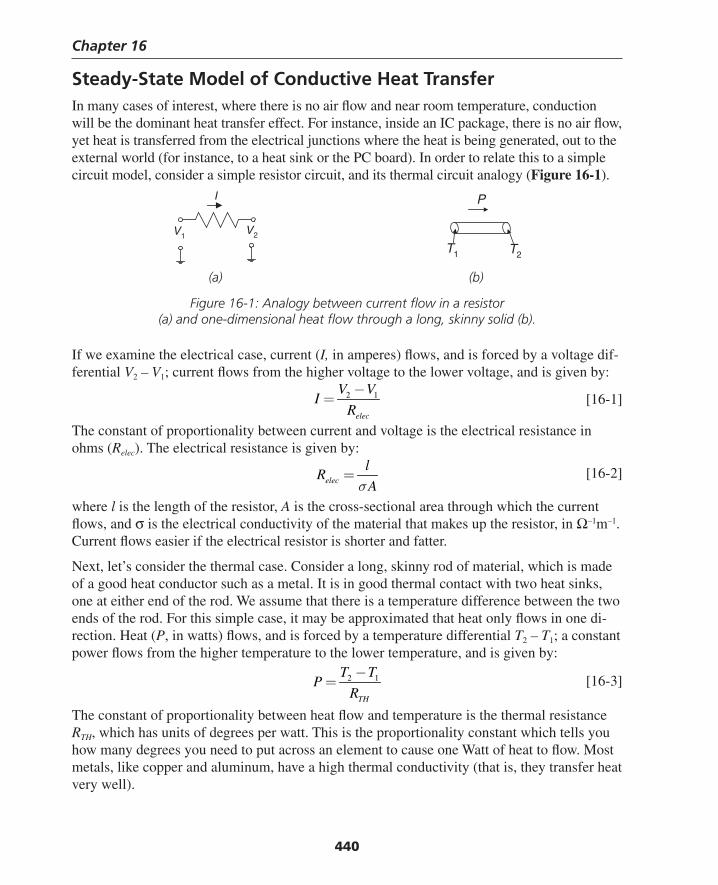
Chapter 16
440
Steady-State Model of Conductive Heat TransferIn many cases of interest, where there is no air fl ow and near room temperature, conduction will be the dominant heat transfer effect. For instance, inside an IC package, there is no air fl ow, yet heat is transferred from the electrical junctions where the heat is being generated, out to the external world (for instance, to a heat sink or the PC board). In order to relate this to a simple circuit model, consider a simple resistor circuit, and its thermal circuit analogy (Figure 16-1).
(a) (b)
Figure 16-1: Analogy between current fl ow in a resistor (a) and one-dimensional heat fl ow through a long, skinny solid (b).
If we examine the electrical case, current (I, in amperes) fl ows, and is forced by a voltage dif-ferential V2 – V1; current fl ows from the higher voltage to the lower voltage, and is given by:
2 1
elec
V VI
R
−= [16-1]
The constant of proportionality between current and voltage is the electrical resistance in ohms (Relec). The electrical resistance is given by:
elec
lR
Aσ= [16-2]
where l is the length of the resistor, A is the cross-sectional area through which the current fl ows, and σ is the electrical conductivity of the material that makes up the resistor, in Ω–1m–1. Current fl ows easier if the electrical resistor is shorter and fatter.
Next, let’s consider the thermal case. Consider a long, skinny rod of material, which is made of a good heat conductor such as a metal. It is in good thermal contact with two heat sinks, one at either end of the rod. We assume that there is a temperature difference between the two ends of the rod. For this simple case, it may be approximated that heat only fl ows in one di-rection. Heat (P, in watts) fl ows, and is forced by a temperature differential T2 – T1; a constant power fl ows from the higher temperature to the lower temperature, and is given by:
2 1
TH
T TP
R
−= [16-3]
The constant of proportionality between heat fl ow and temperature is the thermal resistance RTH, which has units of degrees per watt. This is the proportionality constant which tells you how many degrees you need to put across an element to cause one Watt of heat to fl ow. Most metals, like copper and aluminum, have a high thermal conductivity (that is, they transfer heat very well).
I
V1V2
P
T1 T2
Thompson Book.indb 440 3/20/2006 11:37:28 AM
Other Useful Design Techniques and Loose Ends
441
Analogous to electrical resistance, thermal resistance is given by:
TH
lR
kA= [16-4]
where l is the length of the material through which heat fl ows, A is the cross-sectional area through which the heat fl ows, and k is the thermal conductivity of the material that makes up the resistor, in watts/(meter-degree). As in the electrical case, thermal resistance is lower if the conducting path is shorter and has more area.
Still air, which is a good insulator, has a thermal conductivity k ≈ 0.03 watt/meter-°C. Copper, which is a good conductor of heat, has k ≈ 400 watt/meter-°C. These numbers illustrate why styrofoam, which is full of trapped air, is a good insulator, while copper and aluminum are not. This is one reason why metals aren’t often used as thermal insulators!
Thermal Energy StorageThe effects of energy storage in thermal systems are also demonstrated by analogy. Just as energy is stored in a capacitor as charge on the capacitor plates, energy is stored in the me-chanical structure of a mass, in the vibration of the atoms. A body at a higher temperature has a higher amount of stored energy than the same body at a lower temperature.
In the electrical case, when a linear capacitor is charged from an initial voltage (Vi) to a fi nal voltage (Vf), charge (q, in coulombs) is stored on the plates of the capacitor, as:
( )f iq C V V= − [16-5]
where C is electrical capacitance, in coulombs per volt. During charging, a current fl ows into the capacitor, as:
( )dv tdq
i Cdt dt
= = [16-6]
The charge that fl ows during the charging interval is stored on the plates of the capacitor.
In the thermal case, the thermal capacitance of a mass determines how well the mass stores energy; the units of heat capacity are joules per degree. The thermal capacitance is given by:
TH v vC Mc V cρ= = [16-7]
where ρ is the density of the material (kg/m3), M is the total mass of the material that is being heated or cooled (kg), V is the volume of the material (m3) that is being heated or cooled, and cv is a material property called specifi c heat which is a material property (joules/kg-degree).
When a mass is heated from an initial temperature (Ti) to a fi nal temperature (Tf), energy (E, in joules, or watt-seconds) must be added to the mass to heat it up, as:
( )TH f iE C T T= − [16-8]
Thompson Book.indb 441 3/20/2006 11:37:29 AM
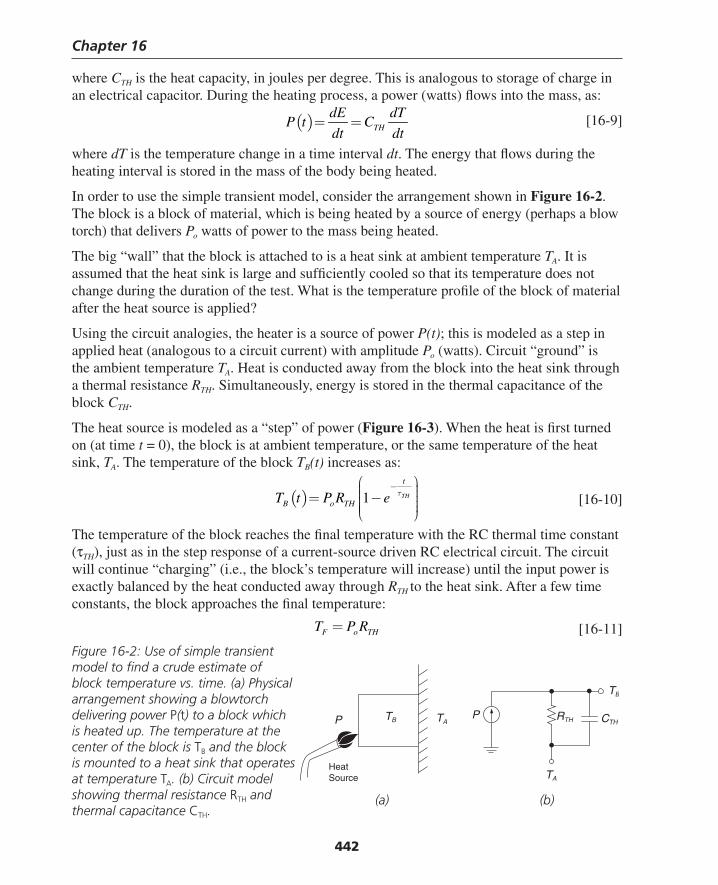
Chapter 16
442
where CTH is the heat capacity, in joules per degree. This is analogous to storage of charge in an electrical capacitor. During the heating process, a power (watts) fl ows into the mass, as:
( ) TH
dE dTP t C
dt dt= = [16-9]
where dT is the temperature change in a time interval dt. The energy that fl ows during the heating interval is stored in the mass of the body being heated.
In order to use the simple transient model, consider the arrangement shown in Figure 16-2. The block is a block of material, which is being heated by a source of energy (perhaps a blow torch) that delivers Po watts of power to the mass being heated.
The big “wall” that the block is attached to is a heat sink at ambient temperature TA. It is assumed that the heat sink is large and suffi ciently cooled so that its temperature does not change during the duration of the test. What is the temperature profi le of the block of material after the heat source is applied?
Using the circuit analogies, the heater is a source of power P(t); this is modeled as a step in applied heat (analogous to a circuit current) with amplitude Po (watts). Circuit “ground” is the ambient temperature TA. Heat is conducted away from the block into the heat sink through a thermal resistance RTH. Simultaneously, energy is stored in the thermal capacitance of the block CTH.
The heat source is modeled as a “step” of power (Figure 16-3). When the heat is fi rst turned on (at time t = 0), the block is at ambient temperature, or the same temperature of the heat sink, TA. The temperature of the block TB(t) increases as:
( ) 1 TH
t
B o THT t P R e τ−⎛ ⎞⎟⎜ ⎟⎜= − ⎟⎜ ⎟⎜ ⎟⎜⎝ ⎠
[16-10]
The temperature of the block reaches the fi nal temperature with the RC thermal time constant (τTH), just as in the step response of a current-source driven RC electrical circuit. The circuit will continue “charging” (i.e., the block’s temperature will increase) until the input power is exactly balanced by the heat conducted away through RTH to the heat sink. After a few time constants, the block approaches the fi nal temperature:
F o THT P R= [16-11]
Figure 16-2: Use of simple transient model to fi nd a crude estimate of block temperature vs. time. (a) Physical arrangement showing a blowtorch delivering power P(t) to a block which is heated up. The temperature at the center of the block is TB and the block is mounted to a heat sink that operates at temperature TA. (b) Circuit model showing thermal resistance RTH and thermal capacitance CTH.
TB
CTHRTH
TA
PTBP
HeatSource
TA
(a) (b)
Thompson Book.indb 442 3/20/2006 11:37:29 AM
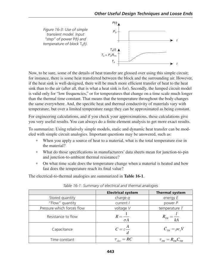
Other Useful Design Techniques and Loose Ends
443
Now, to be sure, some of the details of heat transfer are glossed over using this simple circuit; for instance, there is some heat transferred between the block and the surrounding air. However, if the heat sink is well-designed, there will be much more effi cient transfer of heat to the heat sink than to the air (after all, that is what a heat sink is for). Secondly, the lumped circuit model is valid only for “low frequencies,” or for temperatures that change on a time scale much longer than the thermal time constant. That means that the temperature throughout the body changes the same everywhere. And, the specifi c heat and thermal conductivity of materials vary with temperature, but over a limited temperature range they can be approximated as being constant.
For engineering calculations, and if you check your approximations, these calculations give you very useful results. You can always do a fi nite element analysis to get more exact results.
To summarize: Using relatively simple models, static and dynamic heat transfer can be mod-eled with simple circuit analogies. Important questions may be answered, such as:
• When you apply a source of heat to a material, what is the total temperature rise in the material?
• What do those specifi cations in manufacturers’ data sheets mean for junction-to-pin and junction-to-ambient thermal resistance?
• On what time scale does the temperature change when a material is heated and how fast does the temperature reach its fi nal value?
The electrical-to-thermal analogies are summarized in Table 16-1.
Table 16-1: Summary of electrical and thermal analogies
Electrical system Thermal systemStored quantity charge q energy E“Flow” quantity current I power P
Pressure which forces fl ow voltage V temperature T
Resistance to fl ow1
RAσ
= TH
lR
kA=
CapacitanceA
Cd
ε= TH vC c Vρ=
Time constant elec RCτ = TH TH THR Cτ =
t
t
P(t)
PO
TB(t)
TA + PORTH
TA
Figure 16-3: Use of simple transient model. Input
“step” of power P(t) and temperature of block TB(t).
Thompson Book.indb 443 3/20/2006 11:37:30 AM
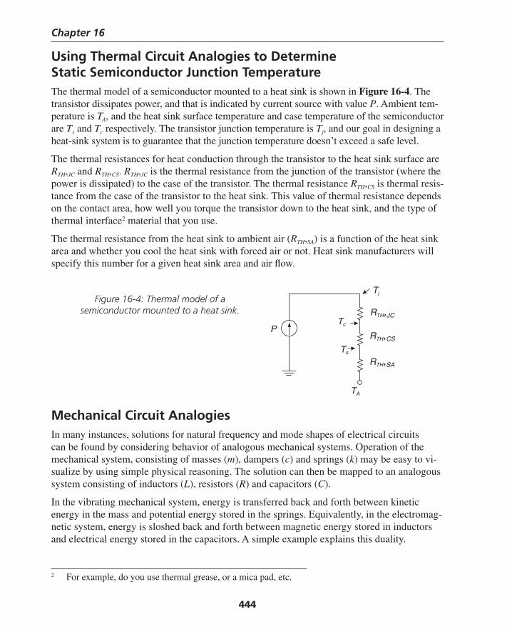
Chapter 16
444
Using Thermal Circuit Analogies to Determine Static Semiconductor Junction TemperatureThe thermal model of a semiconductor mounted to a heat sink is shown in Figure 16-4. The transistor dissipates power, and that is indicated by current source with value P. Ambient tem-perature is TA, and the heat sink surface temperature and case temperature of the semiconductor are Ts and Tc respectively. The transistor junction temperature is Tj, and our goal in designing a heat-sink system is to guarantee that the junction temperature doesn’t exceed a safe level.
The thermal resistances for heat conduction through the transistor to the heat sink surface are RTH,JC and RTH,CS. RTH,JC is the thermal resistance from the junction of the transistor (where the power is dissipated) to the case of the transistor. The thermal resistance RTH,CS is thermal resis-tance from the case of the transistor to the heat sink. This value of thermal resistance depends on the contact area, how well you torque the transistor down to the heat sink, and the type of thermal interface2 material that you use.
The thermal resistance from the heat sink to ambient air (RTH,SA) is a function of the heat sink area and whether you cool the heat sink with forced air or not. Heat sink manufacturers will specify this number for a given heat sink area and air fl ow.
2 For example, do you use thermal grease, or a mica pad, etc.
Mechanical Circuit AnalogiesIn many instances, solutions for natural frequency and mode shapes of electrical circuits can be found by considering behavior of analogous mechanical systems. Operation of the mechanical system, consisting of masses (m), dampers (c) and springs (k) may be easy to vi-sualize by using simple physical reasoning. The solution can then be mapped to an analogous system consisting of inductors (L), resistors (R) and capacitors (C).
In the vibrating mechanical system, energy is transferred back and forth between kinetic energy in the mass and potential energy stored in the springs. Equivalently, in the electromag-netic system, energy is sloshed back and forth between magnetic energy stored in inductors and electrical energy stored in the capacitors. A simple example explains this duality.
Tc
RTH,JC
P
Ts
RTH,CS
RTH,SA
TA
TjFigure 16-4: Thermal model of a
semiconductor mounted to a heat sink.
Thompson Book.indb 444 3/20/2006 11:37:31 AM
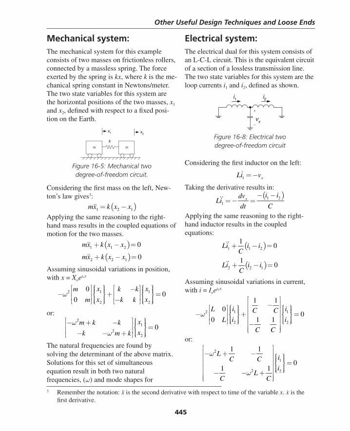
Other Useful Design Techniques and Loose Ends
445
Mechanical system:The mechanical system for this example consists of two masses on frictionless rollers, connected by a massless spring. The force exerted by the spring is kx, where k is the me-chanical spring constant in Newtons/meter. The two state variables for this system are the horizontal positions of the two masses, x1 and x2, defi ned with respect to a fi xed posi-tion on the Earth.
Figure 16-5: Mechanical two degree-of-freedom circuit.
Considering the fi rst mass on the left, New-ton’s law gives3:
( )1 2 1mx k x x= −Applying the same reasoning to the right-hand mass results in the coupled equations of motion for the two masses.
( )( )
1 1 2
2 2 1
0
0
mx k x x
mx k x x
+ − =
+ − =
Assuming sinusoidal variations in position, with x = Xoejωt
1 12
2 2
00
0
x xm k k
x xm k kω
⎧ ⎫ ⎧ ⎫⎡ ⎤ ⎡ ⎤−⎪ ⎪ ⎪ ⎪⎪ ⎪ ⎪ ⎪⎢ ⎥ ⎢ ⎥− + =⎨ ⎬ ⎨ ⎬⎢ ⎥ ⎢ ⎥⎪ ⎪ ⎪ ⎪−⎣ ⎦ ⎣ ⎦⎪ ⎪ ⎪ ⎪⎩ ⎭ ⎩ ⎭
or:2
1
22
0xm k k
xk m k
ωω
⎡ ⎤ ⎧ ⎫⎪ ⎪− + − ⎪ ⎪⎢ ⎥ =⎨ ⎬⎢ ⎥⎪ ⎪− − + ⎪ ⎪⎩ ⎭⎣ ⎦The natural frequencies are found by solving the determinant of the above matrix. Solutions for this set of simultaneous equation result in both two natural frequencies, (ω) and mode shapes for
m m
k
x1 x2
Electrical system: The electrical dual for this system consists of an L-C-L circuit. This is the equivalent circuit of a section of a lossless transmission line. The two state variables for this system are the loop currents i1 and i2, defi ned as shown.
Figure 16-8: Electrical two degree-of-freedom circuit
Considering the fi rst inductor on the left:
1 xLi v= −
Taking the derivative results in:( )1 2
1x
i idvLi
dt C
− −= − =
Applying the same reasoning to the right-hand inductor results in the coupled equations:
( )
( )
1 1 2
2 2 1
10
10
Li i iC
Li i iC
+ − =
+ − =
Assuming sinusoidal variations in current, with i = Ioejωt
1 12
2 2
1 10
00 1 1
i iL C Ci iL
C C
ω
⎡ ⎤⎢ ⎥−⎧ ⎫ ⎧ ⎫⎡ ⎤⎪ ⎪ ⎪ ⎪⎢ ⎥⎪ ⎪ ⎪ ⎪⎢ ⎥− + =⎢ ⎥⎨ ⎬ ⎨ ⎬⎢ ⎥⎪ ⎪ ⎪ ⎪⎢ ⎥⎣ ⎦⎪ ⎪ ⎪ ⎪⎩ ⎭ ⎩ ⎭−⎢ ⎥⎢ ⎥⎣ ⎦
or:
2
1
2 2
1 1
01 1
LiC Ci
LC C
ω
ω
⎡ ⎤⎢ ⎥− + − ⎧ ⎫⎪ ⎪⎢ ⎥⎪ ⎪ =⎢ ⎥⎨ ⎬⎪ ⎪⎢ ⎥⎪ ⎪⎩ ⎭− − +⎢ ⎥⎢ ⎥⎣ ⎦
i1 i2
+
−vx
3 Remember the notation: x is the second derivative with respect to time of the variable x. x is the fi rst derivative.
Thompson Book.indb 445 3/20/2006 11:37:31 AM
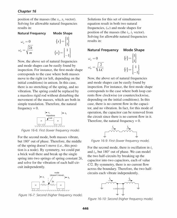
Chapter 16
446
position of the masses (the x1, x2 vector). Solving for allowable natural frequencies results in:
Natural Frequency Mode Shape
0
2
a
b
k
m
ω
ω
=
=
{ }
{ }
1
1
1
1
x
x
⎧ ⎫⎪ ⎪⎪ ⎪= ⎨ ⎬⎪ ⎪⎪ ⎪⎩ ⎭⎧ ⎫⎪ ⎪⎪ ⎪= ⎨ ⎬⎪ ⎪−⎪ ⎪⎩ ⎭
Now, the above set of natural frequencies and mode shapes can be easily found by inspection. For instance, the fi rst mode shape corresponds to the case where both masses move to the right (or left, depending on the initial conditions) in unison. In this case, there is no stretching of the spring, and no vibration. The spring could be replaced by a massless rigid rod without disturbing the movement of the masses, which are both in simple translation. Therefore, the natural frequency = 0.
Figure 16-6: First (lower frequency mode).
For the second mode, both masses vibrate, but 180° out of phase. Therefore, the middle of the spring doesn’t move (i.e., this posi-tion is a node). By symmetry, we could put a brick wall there and break up the single spring into two springs of spring constant 2k, and solve for the vibration of each half-cir-cuit independently.
m m
x1 x2massless
rod
Figure 16-7: Second (higher frequency mode).
m m
2k 2k
x1 x2
node(doesn't move)
Solutions for this set of simultaneous equation result in both two natural frequencies, (ω) and mode shapes for position of the masses (the i1, i2 vector). Solving for allowable natural frequencies results in:
Natural Frequency Mode Shape
0
2
a
b LC
ω
ω
=
=
{}
{}
1
1
1
1
i
i
⎧ ⎫⎪ ⎪⎪ ⎪= ⎨ ⎬⎪ ⎪⎪ ⎪⎩ ⎭⎧ ⎫⎪ ⎪⎪ ⎪= ⎨ ⎬⎪ ⎪−⎪ ⎪⎩ ⎭
Now, the above set of natural frequencies and mode shapes can be easily found by inspection. For instance, the fi rst mode shape corresponds to the case where both loop cur-rents fl ow clockwise (or counterclockwise, depending on the initial conditions). In this case, there is no current fl ow in the capaci-tor, and no vibration. In fact, for this mode of operation, the capacitor can be removed from the circuit since there is no current fl ow in it. Therefore, the natural frequency = 0.
Figure 16-9: First (lower frequency mode).
For the second mode, there is oscillation in i1 and i2, but 180° out of phase. We can model the two half-circuits by breaking up the capacitor into two capacitors, each of value C/2. By symmetry, there is no current fl ow across the boundary. Therefore, the two half-circuits each vibrate independently.
i1 i2
Figure 16-10: Second (higher frequency mode).
C/2
i1 i2
C/2
Thompson Book.indb 446 3/20/2006 11:37:33 AM
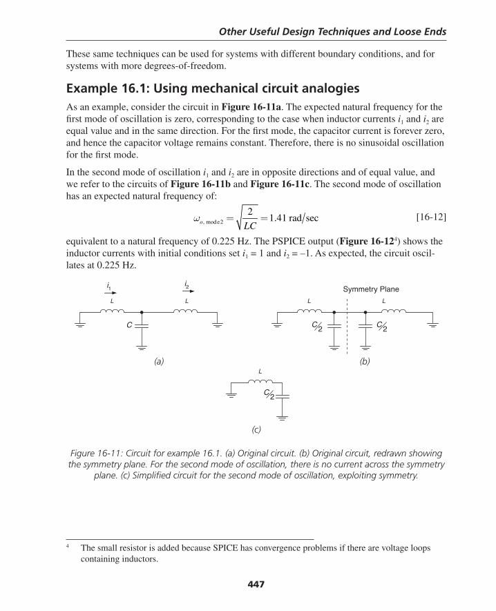
Other Useful Design Techniques and Loose Ends
447
These same techniques can be used for systems with different boundary conditions, and for systems with more degrees-of-freedom.
Example 16.1: Using mechanical circuit analogiesAs an example, consider the circuit in Figure 16-11a. The expected natural frequency for the fi rst mode of oscillation is zero, corresponding to the case when inductor currents i1 and i2 are equal value and in the same direction. For the fi rst mode, the capacitor current is forever zero, and hence the capacitor voltage remains constant. Therefore, there is no sinusoidal oscillation for the fi rst mode.
In the second mode of oscillation i1 and i2 are in opposite directions and of equal value, and we refer to the circuits of Figure 16-11b and Figure 16-11c. The second mode of oscillation has an expected natural frequency of:
, mod e2
21.41 rad seco LC
ω = = [16-12]
equivalent to a natural frequency of 0.225 Hz. The PSPICE output (Figure 16-124) shows the inductor currents with initial conditions set i1 = 1 and i2 = –1. As expected, the circuit oscil-lates at 0.225 Hz.
4 The small resistor is added because SPICE has convergence problems if there are voltage loops containing inductors.
i1 i2
L L
C
L L
L
2C
Symmetry Plane
2C
2C
(a) (b)
(c)
Figure 16-11: Circuit for example 16.1. (a) Original circuit. (b) Original circuit, redrawn showing the symmetry plane. For the second mode of oscillation, there is no current across the symmetry
plane. (c) Simplifi ed circuit for the second mode of oscillation, exploiting symmetry.
Thompson Book.indb 447 3/20/2006 11:37:34 AM
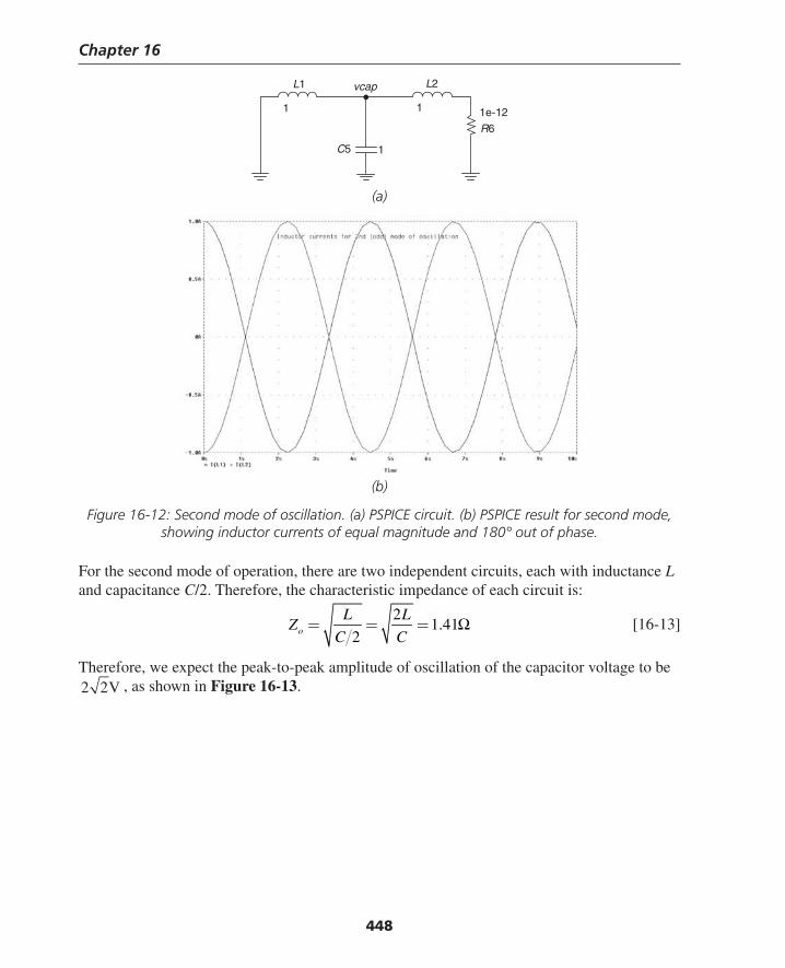
Chapter 16
448
(a)
L2
1
1C5
1
L1
R6
vcap
1e-12
(b)
Figure 16-12: Second mode of oscillation. (a) PSPICE circuit. (b) PSPICE result for second mode, showing inductor currents of equal magnitude and 180° out of phase.
For the second mode of operation, there are two independent circuits, each with inductance L and capacitance C/2. Therefore, the characteristic impedance of each circuit is:
2
1.412o
L LZ
C C= = = Ω [16-13]
Therefore, we expect the peak-to-peak amplitude of oscillation of the capacitor voltage to be2 2V , as shown in Figure 16-13.
Thompson Book.indb 448 3/20/2006 11:37:34 AM
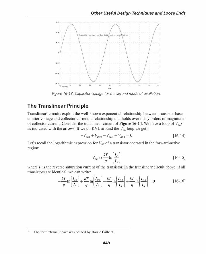
Other Useful Design Techniques and Loose Ends
449
Figure 16-13: Capacitor voltage for the second mode of oscillation.
The Translinear PrincipleTranslinear5 circuits exploit the well-known exponential relationship between transistor base-emitter voltage and collector current, a relationship that holds over many orders of magnitude of collector current. Consider the translinear circuit of Figure 16-14. We have a loop of VBEs as indicated with the arrows. If we do KVL around the VBE loop we get:
1 2 3 4 0BE BE BE BEV V V V− + − + = [16-14]
Let’s recall the logarithmic expression for VBE of a transistor operated in the forward-active region:
ln CBE
S
IkTV
q I
⎛ ⎞⎟⎜ ⎟≈ ⎜ ⎟⎜ ⎟⎜⎝ ⎠ [16-15]
where IS is the reverse saturation current of the transistor. In the translinear circuit above, if all transistors are identical, we can write:
1 2 3 4ln ln ln ln 0C C C C
S S S S
I I I IkT kT kT kT
q I q I q I q I
⎛ ⎞ ⎛ ⎞ ⎛ ⎞ ⎛ ⎞⎟ ⎟ ⎟ ⎟⎜ ⎜ ⎜ ⎜⎟ ⎟ ⎟ ⎟− + − + =⎜ ⎜ ⎜ ⎜⎟ ⎟ ⎟ ⎟⎜ ⎜ ⎜ ⎜⎟ ⎟ ⎟ ⎟⎜ ⎜ ⎜ ⎜⎝ ⎠ ⎝ ⎠ ⎝ ⎠ ⎝ ⎠ [16-16]
5 The term “translinear” was coined by Barrie Gilbert.
Thompson Book.indb 449 3/20/2006 11:37:35 AM
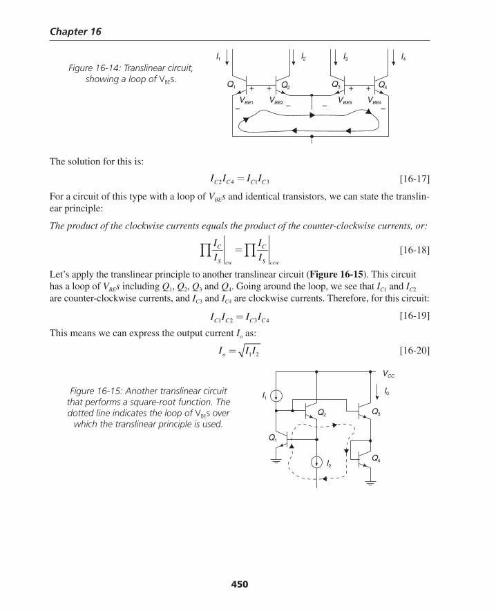
Chapter 16
450
The solution for this is:
2 4 1 3C C C CI I I I= [16-17]
For a circuit of this type with a loop of VBEs and identical transistors, we can state the translin-ear principle:
The product of the clockwise currents equals the product of the counter-clockwise currents, or:
C C
S Scw ccw
I I
I I=∏ ∏ [16-18]
Let’s apply the translinear principle to another translinear circuit (Figure 16-15). This circuit has a loop of VBEs including Q1, Q2, Q3 and Q4. Going around the loop, we see that IC1 and IC2 are counter-clockwise currents, and IC3 and IC4 are clockwise currents. Therefore, for this circuit:
1 2 3 4C C C CI I I I= [16-19]
This means we can express the output current Io as:
1 2oI I I= [16-20]
I4I3I2I1
+ + + +
− −− −VBE1 VBE2 VBE3 VBE4
Q1 Q2 Q3 Q4
Figure 16-14: Translinear circuit, showing a loop of VBEs.
Figure 16-15: Another translinear circuit that performs a square-root function. The dotted line indicates the loop of VBEs over
which the translinear principle is used.
I0
I2
I1
Q3
Q4
Q1
Q2
VCC
Thompson Book.indb 450 3/20/2006 11:37:36 AM
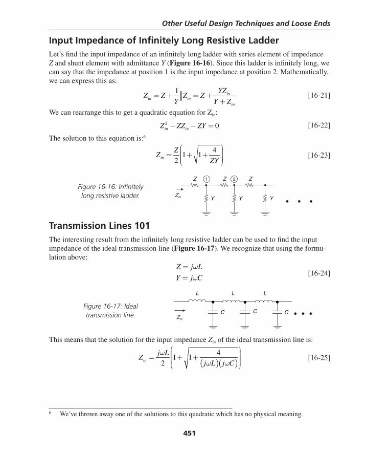
Other Useful Design Techniques and Loose Ends
451
Input Impedance of Infi nitely Long Resistive LadderLet’s fi nd the input impedance of an infi nitely long ladder with series element of impedance Z and shunt element with admittance Y (Figure 16-16). Since this ladder is infi nitely long, we can say that the impedance at position 1 is the input impedance at position 2. Mathematically, we can express this as:
1 in
in inin
YZZ Z Z Z
Y Y Z= + = +
+ [16-21]
We can rearrange this to get a quadratic equation for Zin:
2 0in inZ ZZ ZY− − = [16-22]
The solution to this equation is:6
4
1 12in
ZZ
ZY
⎛ ⎞⎟⎜ ⎟⎜= + + ⎟⎜ ⎟⎟⎜⎝ ⎠ [16-23]
6 We’ve thrown away one of the solutions to this quadratic which has no physical meaning.
Transmission Lines 101The interesting result from the infi nitely long resistive ladder can be used to fi nd the input impedance of the ideal transmission line (Figure 16-17). We recognize that using the formu-lation above:
Z j L
Y j C
ωω
==
[16-24]
• • •YZin Y Y
Z Z Z1 2
Figure 16-16: Infi nitely long resistive ladder.
This means that the solution for the input impedance Zin of the ideal transmission line is:
( )( )
41 1
2in
j LZ
j L j C
ωω ω
⎛ ⎞⎟⎜ ⎟⎜= + + ⎟⎜ ⎟⎜ ⎟⎜⎝ ⎠ [16-25]
L L L
C C C • • •Zin
Figure 16-17: Ideal transmission line.
Thompson Book.indb 451 3/20/2006 11:37:36 AM
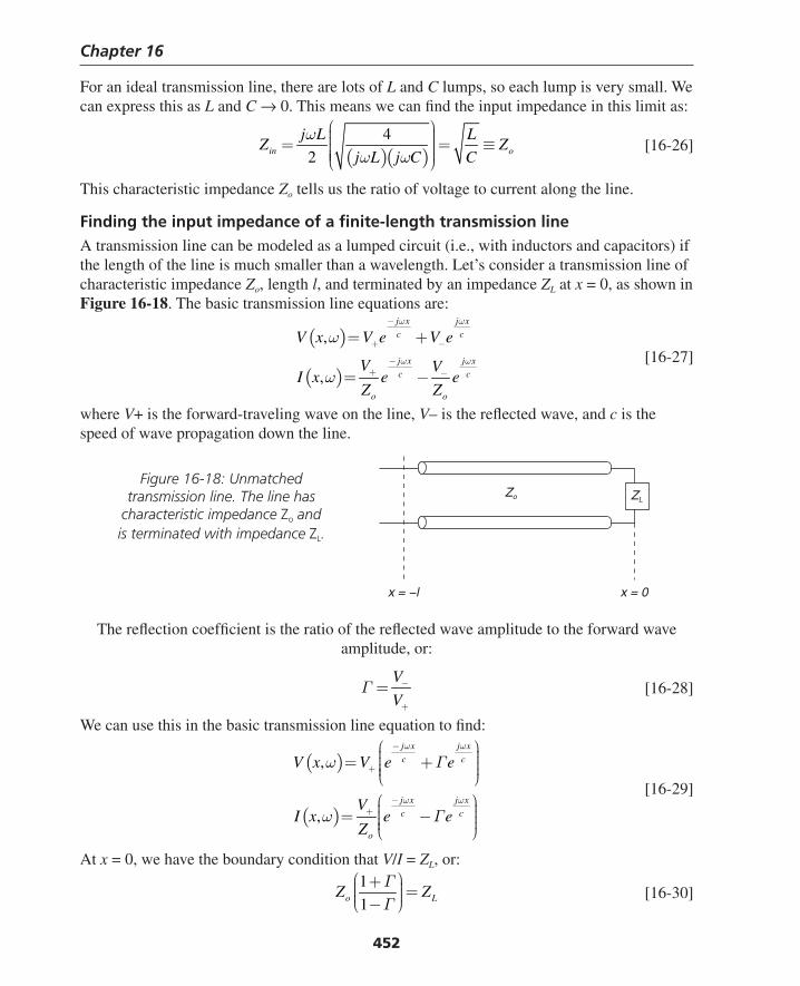
Chapter 16
452
For an ideal transmission line, there are lots of L and C lumps, so each lump is very small. We can express this as L and C → 0. This means we can fi nd the input impedance in this limit as:
( )( )
4
2in o
j L LZ Z
j L j C C
ωω ω
⎛ ⎞⎟⎜ ⎟⎜= = ≡⎟⎜ ⎟⎜ ⎟⎜⎝ ⎠ [16-26]
This characteristic impedance Zo tells us the ratio of voltage to current along the line.
Finding the input impedance of a fi nite-length transmission lineA transmission line can be modeled as a lumped circuit (i.e., with inductors and capacitors) if the length of the line is much smaller than a wavelength. Let’s consider a transmission line of characteristic impedance Zo, length l, and terminated by an impedance ZL at x = 0, as shown in Figure 16-18. The basic transmission line equations are:
( )
( )
,
,
j x j x
c c
j x j x
c c
o o
V x V e V e
V VI x e e
Z Z
ω ω
ω ω
ω
ω
−
+ −
−+ −
= +
= − [16-27]
where V+ is the forward-traveling wave on the line, V– is the refl ected wave, and c is the speed of wave propagation down the line.
The refl ection coeffi cient is the ratio of the refl ected wave amplitude to the forward wave amplitude, or:
V
VΓ −
+
= [16-28]
We can use this in the basic transmission line equation to fi nd:
( )
( )
,
,
j x j x
c c
j x j x
c c
o
V x V e e
VI x e e
Z
ω ω
ω ω
ω Γ
ω Γ
−
+
−+
⎛ ⎞⎟⎜ ⎟= +⎜ ⎟⎜ ⎟⎜⎝ ⎠⎛ ⎞⎟⎜ ⎟= −⎜ ⎟⎜ ⎟⎜⎝ ⎠
[16-29]
At x = 0, we have the boundary condition that V/I = ZL, or:
1
1o LZ ZΓΓ
⎛ ⎞+ ⎟⎜ =⎟⎜ ⎟⎜⎝ ⎠− [16-30]
Zo
x = −l x = 0
ZL
Figure 16-18: Unmatched transmission line. The line has
characteristic impedance Zo and is terminated with impedance ZL.
Thompson Book.indb 452 3/20/2006 11:37:37 AM
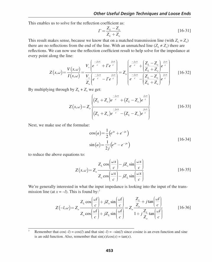
Other Useful Design Techniques and Loose Ends
453
This enables us to solve for the refl ection coeffi cient as:
L o
L o
Z Z
Z ZΓ
−=
+ [16-31]
This result makes sense, because we know that on a matched transmission line (with ZL = Zo) there are no refl ections from the end of the line. With an unmatched line (ZL ≠ Zo) there are refl ections. We can now use the refl ection coeffi cient result to help solve for the impedance at every point along the line:
( )
( )( )
,,
,
j x j x j x j xL oc c c c
L oo j x j xj x j x
L oc cc c
L oo
Z ZV e e e e
V x Z ZZ x Z
I x V Z Ze ee e
Z ZZ
ω ω ω ω
ω ωω ω
Γω
ωω
Γ
− −
+
−−+
⎛ ⎞⎛ ⎞ ⎛ ⎞− ⎟⎟ ⎜ ⎟⎜ ⎜ ⎟⎟ ⎟+ ⎜⎜ +⎜ ⎟⎟ ⎟⎜⎜ ⎜ ⎟⎟ ⎟⎜ ⎜ +⎜⎝ ⎠ ⎝ ⎠ ⎟⎜ ⎟= = = ⎜ ⎟⎟⎜⎛ ⎞ ⎛ ⎞− ⎟⎜⎟ ⎟⎜ ⎜ ⎟⎜⎟ ⎟−−⎜ ⎜ ⎟⎜⎟ ⎟ ⎟⎜ ⎜ ⎟⎜⎟ ⎜ ⎟⎜ ⎜ +⎝ ⎠⎝ ⎠ ⎝ ⎠
[16-32]
By multiplying through by ZL + Zo we get:
( )( ) ( )
( ) ( ),
j x j x
c cL o L o
o j x j x
c cL o L o
Z Z e Z Z e
Z x Z
Z Z e Z Z e
ω ω
ω ωω
−
−
⎛ ⎞⎟⎜ ⎟+ + −⎜ ⎟⎜ ⎟⎜⎝ ⎠=
⎛ ⎞⎟⎜ ⎟+ − −⎜ ⎟⎜ ⎟⎜⎝ ⎠
[16-33]
Next, we make use of the formulae:
( ) ( )
( ) ( )
1cos
21
sin2
ja ja
ja ja
a e e
a e ej
−
−
= +
= − [16-34]
to reduce the above equations to:
( )cos sin
,cos sin
L o
o
o L
x xZ jZ
c cZ x Z
x xZ jZ
c c
ω ω
ωω ω
⎛ ⎞ ⎛ ⎞⎟ ⎟⎜ ⎜−⎟ ⎟⎜ ⎜⎟ ⎟⎜ ⎜⎝ ⎠ ⎝ ⎠=
⎛ ⎞ ⎛ ⎞⎟ ⎟⎜ ⎜−⎟ ⎟⎜ ⎜⎟ ⎟⎜ ⎜⎝ ⎠ ⎝ ⎠
[16-35]
We’re generally interested in what the input impedance is looking into the input of the trans-mission line (at x = –l). This is found by:7
( )tancos sin
,cos sin 1 tan
LL o
oo o
Lo L
o
Z ll ljZ jZ
Z cc cZ l Z Z
Zl l lZ jZ j
c c Z c
ωω ω
ωω ω ω
⎛ ⎞⎛ ⎞ ⎛ ⎞ ⎟⎟ ⎟ ⎜⎜ ⎜ ++ ⎟⎟ ⎟ ⎜⎜ ⎜ ⎟⎟ ⎟ ⎜⎜ ⎜ ⎝ ⎠⎝ ⎠ ⎝ ⎠− = =
⎛ ⎞ ⎛ ⎞ ⎛ ⎞⎟ ⎟ ⎟⎜ ⎜ ⎜+ +⎟ ⎟ ⎟⎜ ⎜ ⎜⎟ ⎟ ⎟⎜ ⎜ ⎜⎝ ⎠ ⎝ ⎠ ⎝ ⎠
[16-36]
7 Remember that cos(–l) = cos(l) and that sin(–l) = –sin(l) since cosine is an even function and sine is an odd function. Also, remember that sin(x)/cos(x) = tan(x).
Thompson Book.indb 453 3/20/2006 11:37:38 AM
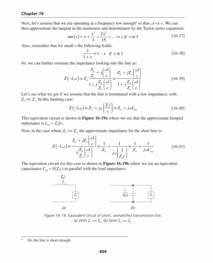
Chapter 16
454
Next, let’s assume that we are operating at a frequency low enough8 so that ωl << c. We can then approximate the tangent in the numerator and denominator by the Taylor series expansion:
( )3 52
tan 13 15
x xx x x if x= + + + ≈… [16-37]
Also, remember that for small x the following holds:
1
1 11
x if xx
≈ −+
[16-38]
So, we can further estimate the impedance looking into the line as:
( ),1 1
LL o
oo
L L
o o
Z l lj Z jZ
Z c cZ l Z
Z Zl lj j
Z c Z c
ω ω
ωω ω
⎛ ⎞ ⎛ ⎞⎟ ⎟⎜ ⎜+ +⎟ ⎟⎜ ⎜⎟ ⎟⎜ ⎜⎝ ⎠ ⎝ ⎠− ≈ ≈
⎛ ⎞ ⎛ ⎞⎟ ⎟⎜ ⎜+ +⎟ ⎟⎜ ⎜⎟ ⎟⎜ ⎜⎝ ⎠ ⎝ ⎠
[16-39]
Let’s see what we get if we assume that the line is terminated with a low impedance, with ZL << Zo. In this limiting case:
( ), oL L eq
Z lZ l Z j Z j L
cω ω ω
⎛ ⎞⎟⎜− ≈ + ≈ +⎟⎜ ⎟⎟⎜⎝ ⎠ [16-40]
This equivalent circuit is shown in Figure 16-19a where we see that the approximate lumped inductance is Leq ≈ Zol/c.
Now, in the case where ZL >> Zo, the approximate impedance for the short line is:
( ) 1 1 1 1,
1
L o
L L L eq
o o
lZ jZ
cZ l
Z l Z Z j Cj j
Z c Z c
ω
ωω ω
ω
⎛ ⎞⎟⎜+ ⎟⎜ ⎟⎜⎝ ⎠− ≈ ≈ + ≈ +
⎛ ⎞ ⎛ ⎞⎟ ⎟⎜ ⎜⎟ ⎟⎜ ⎜⎟ ⎟⎜ ⎜⎝ ⎠ ⎟⎜⎝ ⎠
[16-41]
The equivalent circuit for this case is shown in Figure 16-19b where we see an equivalent capacitance Ceq ≈ l/(Zoc) in parallel with the load impedance.
(a) (b)
Figure 16-19: Equivalent circuit of short, unmatched transmission line. (a) With ZL << Zo. (b) With ZL >> Zo.
ZLZL
oZ l
c
o
lZ c
8 Or, the line is short enough.
Thompson Book.indb 454 3/20/2006 11:37:39 AM
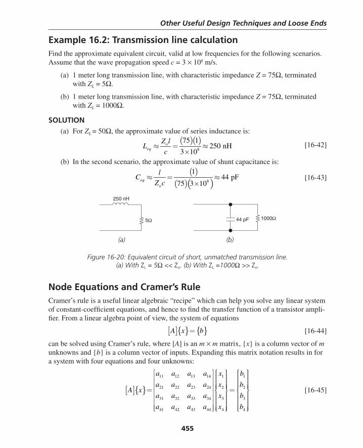
Other Useful Design Techniques and Loose Ends
455
Example 16.2: Transmission line calculation Find the approximate equivalent circuit, valid at low frequencies for the following scenarios. Assume that the wave propagation speed c = 3 × 10⁸ m/s.
(a) 1 meter long transmission line, with characteristic impedance Z = 75Ω, terminated with ZL = 5Ω.
(b) 1 meter long transmission line, with characteristic impedance Z = 75Ω, terminated with ZL = 1000Ω.
SOLUTION(a) For ZL = 50Ω, the approximate value of series inductance is:
( )( )
8
75 1250 nH
3 10o
eq
Z lL
c≈ = ≈
× [16-42]
(b) In the second scenario, the approximate value of shunt capacitance is:
( )
( )( )8
144 pF
75 3 10eq
o
lC
Z c≈ = ≈
× [16-43]
(a) (b)
Figure 16-20: Equivalent circuit of short, unmatched transmission line. (a) With ZL = 5Ω << Zo. (b) With ZL =1000Ω >> Zo.
Node Equations and Cramer’s RuleCramer’s rule is a useful linear algebraic “recipe” which can help you solve any linear system of constant-coeffi cient equations, and hence to fi nd the transfer function of a transistor ampli-fi er. From a linear algebra point of view, the system of equations
[ ]{ } { }A x b= [16-44]
can be solved using Cramer’s rule, where [A] is an m × m matrix, {x} is a column vector of m unknowns and {b} is a column vector of inputs. Expanding this matrix notation results in for a system with four equations and four unknowns:
[ ]{ }
11 12 13 14 1 1
21 22 23 24 2 2
31 32 33 34 3 3
41 42 43 44 4 4
a a a a x b
a a a a x bA x
a a a a x b
a a a a x b
⎡ ⎤ ⎧ ⎫ ⎧ ⎫⎪ ⎪ ⎪ ⎪⎪ ⎪ ⎪ ⎪⎢ ⎥⎪ ⎪ ⎪ ⎪⎢ ⎥⎪ ⎪ ⎪ ⎪⎪ ⎪ ⎪ ⎪⎪ ⎪ ⎪ ⎪⎢ ⎥= =⎨ ⎬ ⎨ ⎬⎢ ⎥⎪ ⎪ ⎪ ⎪⎪ ⎪ ⎪ ⎪⎢ ⎥⎪ ⎪ ⎪ ⎪⎢ ⎥⎪ ⎪ ⎪ ⎪⎪ ⎪ ⎪ ⎪⎢ ⎥⎪ ⎪ ⎪ ⎪⎩ ⎭ ⎩ ⎭⎣ ⎦
[16-45]
5Ω 1000Ω44 pF
250 nH
Thompson Book.indb 455 3/20/2006 11:37:39 AM
Chapter 16
456
Using Cramer’s rule, if you wanted to fi nd unknown x3 you solve the following:
11 12 1 14
21 22 2 24
31 32 3 34
41 42 4 443
11 12 13 14
21 22 23 24
31 32 33 34
41 42 43 44
det
det
a a b a
a a b a
a a b a
a a b ax
a a a a
a a a a
a a a a
a a a a
⎡ ⎤⎢ ⎥⎢ ⎥⎢ ⎥⎢ ⎥⎢ ⎥⎢ ⎥⎢ ⎥⎣ ⎦=⎡ ⎤⎢ ⎥⎢ ⎥⎢ ⎥⎢ ⎥⎢ ⎥⎢ ⎥⎢ ⎥⎣ ⎦
[16-46]
This looks like a mess, but can be easily manipulated using simple linear algebra. The term “det” denotes the “determinant” of a matrix. For a 2 × 2 matrix, the determinant is found as follows:
11 1211 22 12 21
21 22
deta a
a a a aa a
⎡ ⎤⎢ ⎥ = −⎢ ⎥⎣ ⎦
[16-47]
For a 3 × 3 matrix, the determinant is:
( ) ( ) ( )11 12 13
21 22 23 11 22 33 23 32 12 21 33 23 31 13 21 32 22 31
31 32 33
det
a a a
a a a a a a a a a a a a a a a a a a
a a a
⎡ ⎤⎢ ⎥⎢ ⎥ = − − − + −⎢ ⎥⎢ ⎥⎣ ⎦
[16-48]
For an N × N matrix, it’s more complicated but still doable. Consult a linear algebra textbook for the recipe.
Example 16.3: Using Cramer’s rule to solve simultaneous linear equationsLet’s use a simple linear algebra example to show the use of Cramer’s rule. We’ll solve the following simultaneous linear equations for x, y and z.
5
3 3
2 2 3 10
x y z
x y z
x y z
+ + =− + = −
+ + =
[16-49]
Putting this into matrix form results in:
1 1 1 5
1 1 3 3
2 2 3 10
x
y
z
⎡ ⎤ ⎧ ⎫ ⎧ ⎫⎪ ⎪ ⎪ ⎪⎪ ⎪ ⎪ ⎪⎢ ⎥⎪ ⎪ ⎪ ⎪⎪ ⎪ ⎪ ⎪⎢ ⎥− = −⎨ ⎬ ⎨ ⎬⎢ ⎥⎪ ⎪ ⎪ ⎪⎪ ⎪ ⎪ ⎪⎢ ⎥⎪ ⎪ ⎪ ⎪⎪ ⎪ ⎪ ⎪⎣ ⎦⎩ ⎭ ⎩ ⎭
[16-50]
Thompson Book.indb 456 3/20/2006 11:37:40 AM
Other Useful Design Techniques and Loose Ends
457
We solve for x, y and z as follows:
( )( ) ( ) ( )( ) ( ) ( )
( )( ) ( )( ) ( )( )
5 1 1
det 3 1 3
5 3 6 1 9 30 1 6 1010 2 3 21
1 1 1 1 3 6 1 3 6 1 2 2 2
det 1 1 3
2 2 3
1 5 1
det 1 3 3
1 9 30 5 3 6 1 10 62 10 3 84
1 1 1 2 2
det 1 1 3
2 2 3
1 1 5
det 1 1 3
2 2 10
x
y
z
⎡ ⎤⎢ ⎥⎢ ⎥− −⎢ ⎥⎢ ⎥ − − − − − + − + −⎣ ⎦= = = =⎡ ⎤ − − − − + + −⎢ ⎥⎢ ⎥−⎢ ⎥⎢ ⎥⎣ ⎦
⎡ ⎤⎢ ⎥⎢ ⎥−⎢ ⎥⎢ ⎥ − − − − + + −⎣ ⎦= = = =⎡ ⎤ − −⎢ ⎥⎢ ⎥−⎢ ⎥⎢ ⎥⎣ ⎦⎡ ⎤⎢⎢ − −⎢⎢⎣=
( )( ) ( )( ) ( )( )1 10 6 1 10 6 5 2 2 00
1 1 1 2 2
det 1 1 3
2 2 3
⎥⎥⎥⎥ − + − + + +⎦ = = =
⎡ ⎤ − −⎢ ⎥⎢ ⎥−⎢ ⎥⎢ ⎥⎣ ⎦
[16-51]
By direct substitution, we fi nd that the values x = 1, y = 4 and z = 0 are indeed all correct.
Another simple example illustrates the use of Cramer’s rule in the circuit realm. Shown in Figure 16-21 is the small-signal model for a common emitter amplifi er. Let’s generate the node equations and solve for the transfer function using Cramer’s rule.
Figure 16-21: Small-signal model of common-emitter amplifi er.
+
–
rx
rπ Cπ
Cμ
gmvπvπ
vo
RL
Rs
vi
We’ll lump Rs and rx together in a single effective source resistance Rs', with Gs' = 1/Rs'. At node vπ, we sum currents at the junction resulting in:
( ) ( ) 0i s ov v G v C s v r v v C sπ π π π π π μ′− − − + − = [16-52]
Thompson Book.indb 457 3/20/2006 11:37:40 AM
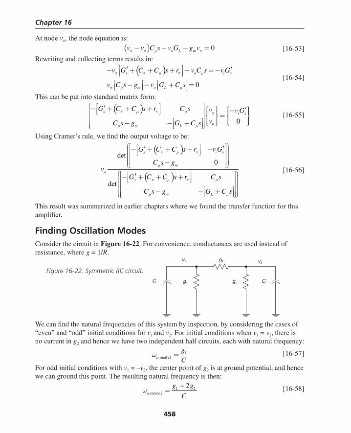
Chapter 16
458
At node vo, the node equation is:
( ) 0o o L mv v C s v G g vπ μ π− − − = [16-53]
Rewriting and collecting terms results in:
( )
0
s o i s
m o L
v G C C s r v C s v G
v C s g v G C s
π π μ π μ
π μ μ
⎡ ⎤′ ′− + + + + = −⎢ ⎥⎣ ⎦⎡ ⎤ ⎡ ⎤− − + =⎢ ⎥ ⎢ ⎥⎣ ⎦ ⎣ ⎦
[16-54]
This can be put into standard matrix form:
( )
0
s i s
om L
G C C s r C s v v G
vC s g G C s
π μ π μ π
μ μ
⎡ ⎤⎡ ⎤′− + + + ⎧ ⎫ ⎧ ⎫′−⎪ ⎪ ⎪ ⎪⎢ ⎥⎢ ⎥⎣ ⎦ ⎪ ⎪ ⎪ ⎪=⎢ ⎥⎨ ⎬ ⎨ ⎬⎪ ⎪ ⎪ ⎪⎢ ⎥⎡ ⎤− − + ⎪ ⎪⎪ ⎪ ⎩ ⎭⎩ ⎭⎢ ⎥⎢ ⎥⎣ ⎦⎣ ⎦
[16-55]
Using Cramer’s rule, we fi nd the output voltage to be:
( )
( )
det0
det
s i s
m
o
s
m L
G C C s r v G
C s gv
G C C s r C s
C s g G C s
π μ π
μ
π μ π μ
μ μ
⎛ ⎞⎡ ⎤⎡ ⎤′ ′ ⎟− + + + −⎜⎢ ⎥⎟⎢ ⎥⎜ ⎣ ⎦ ⎟⎜⎢ ⎥⎟⎜ ⎟⎜⎢ ⎥⎟− ⎟⎜⎝ ⎠⎣ ⎦⎛ ⎞⎡ ⎤⎡ ⎤′ ⎟− + + +⎜⎢ ⎥⎟⎢ ⎥⎜ ⎣ ⎦ ⎟⎜⎢ ⎥⎟⎜ ⎟⎜⎢ ⎥⎡ ⎤ ⎟− − +⎜ ⎟⎢ ⎥⎝ ⎠⎢ ⎥⎣ ⎦⎣ ⎦
[16-56]
This result was summarized in earlier chapters where we found the transfer function for this amplifi er.
Finding Oscillation ModesConsider the circuit in Figure 16-22. For convenience, conductances are used instead of resistance, where g = 1/R.
We can fi nd the natural frequencies of this system by inspection, by considering the cases of “even” and “odd” initial conditions for v1 and v2. For initial conditions when v1 = v2, there is no current in g2 and hence we have two independent half circuits, each with natural frequency:
1,mod e1o
g
Cω = [16-57]
For odd initial conditions with v1 = –v2, the center point of g2 is at ground potential, and hence we can ground this point. The resulting natural frequency is then:
1 2,mod e2
2o
g g
Cω
+= [16-58]
C g1 g1 C
g2v1 v2
Figure 16-22: Symmetric RC circuit.
Thompson Book.indb 458 3/20/2006 11:37:41 AM
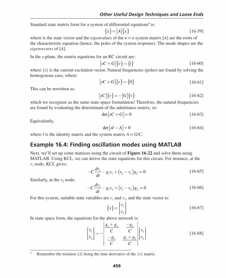
Other Useful Design Techniques and Loose Ends
459
Standard state matrix form for a system of differential equations9 is:
{ } [ ]{ }x A x= [16-59]
where is the state vector and the eigenvalues of the n × n system matrix [A] are the roots of the characteristic equation (hence, the poles of the system response). The mode shapes are the eigenvectors of [A].
In the s-plane, the matrix equations for an RC circuit are:
[ ]{ } {}sC G v i+ = [16-60]
where {i} is the current excitation vector. Natural frequencies (poles) are found by solving the homogenous case, where:
[ ]{ } { }0sC G v+ = [16-61]
This can be rewritten as:
[ ]{ } [ ]{ }sC v G v= − [16-62]
which we recognize as the same state-space formulation! Therefore, the natural frequencies are found by evaluating the determinant of the admittance matrix, or:
[ ]det 0sC G+ = [16-63]
Equivalently,
[ ]det 0sI A− = [16-64]
where I is the identity matrix and the system matrix A = G/C.
Example 16.4: Finding oscillation modes using MATLABNext, we’ll set up some matrices using the circuit of Figure 16-22 and solve them using MATLAB. Using KCL, we can derive the state equations for this circuit. For instance, at the v1 node, KCL gives:
( )11 1 2 1 2 0
dvC g v v v g
dt− − + − = [16-65]
Similarly, at the v2 node:
( )21 2 1 2 2 0
dvC g v v v g
dt− − + − = [16-66]
For this system, suitable state variables are v1 and v2, and the state vector is:
{ } 1
2
vx
v
⎧ ⎫⎪ ⎪⎪ ⎪= ⎨ ⎬⎪ ⎪⎪ ⎪⎩ ⎭ [16-67]
In state space form, the equations for the above network is:
1 2 2
1 1
2 22 1 2
g g gv vC Cv vg g g
C C
⎡ ⎤+ −⎢ ⎥⎧ ⎫ ⎧ ⎫⎪ ⎪ ⎪ ⎪⎢ ⎥⎪ ⎪ ⎪ ⎪= −⎢ ⎥⎨ ⎬ ⎨ ⎬⎪ ⎪ ⎪ ⎪⎢ ⎥− +⎪ ⎪ ⎪ ⎪⎩ ⎭ ⎩ ⎭⎢ ⎥⎢ ⎥⎣ ⎦
[16-68]
9 Remember the notation {x} being the time derivative of the {x} matrix.
Thompson Book.indb 459 3/20/2006 11:37:42 AM

Chapter 16
460
Following is a MATLAB script for fi nding the natural frequencies of this system, assuming that g1 = 1Ω–1, g2 = 10Ω–1 and C = 1 farad:
function RC
g1=1; g2=10;
% Conductance
C=1;
% Capacitors
% Form A matrix
A=-[(g1+g2)/C -g2/C;
-g2/C (g1+g2)/C];
% Find natural frequencies and mode shapes
[Modeshapes, NatFreqs] = eig(A);
% Normalize modeshapes
N=size(Modeshapes,1);
for i=1:N
Modeshapes(:,i)=Modeshapes(:,i)/max(abs(Modeshapes(:,i)));
end
% Display modeshapes
Natural_Frequencies=NatFreqs
Mode_Shapes=Modeshapes
And here’s the result of running this MATLAB script, where we fi nd the natural frequencies and mode shapes. The natural frequencies are the diagonals of the natural frequency matrix. The mode shapes are the columns of the eigenvector matrix. For instance, for ωo = –1 radian/second, the mode shape is [1 1], corresponding to the case when initial conditions are set as v1 = v2. For ωo = –20 radian/second, the mode shape is [1 –1], corresponding to the case when v1 = –v2.
» RC
Natural_Frequencies =
–21 0
0 –1
Mode_Shapes =
1 1
–1 1
Note that the natural frequencies are the same as calculated by the “inspection” method.
Thompson Book.indb 460 3/20/2006 11:37:42 AM
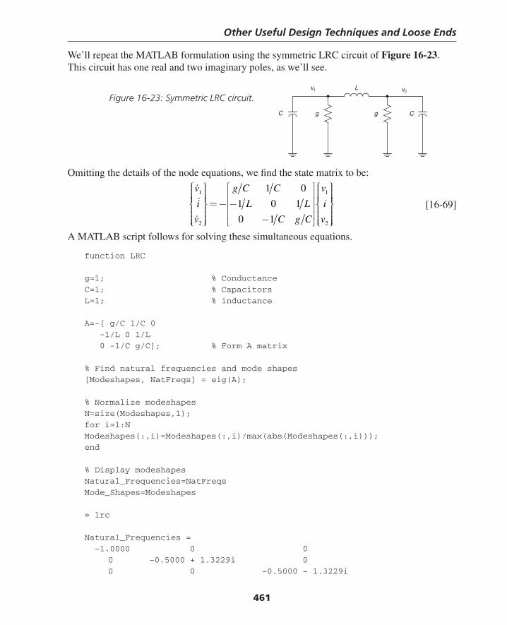
Other Useful Design Techniques and Loose Ends
461
We’ll repeat the MATLAB formulation using the symmetric LRC circuit of Figure 16-23. This circuit has one real and two imaginary poles, as we’ll see.
Omitting the details of the node equations, we fi nd the state matrix to be:
1 1
2 2
1 0
1 0 1
0 1
v g C C v
i L L i
v C g C v
⎧ ⎫ ⎡ ⎤⎧ ⎫⎪ ⎪ ⎪ ⎪⎪ ⎪ ⎪ ⎪⎢ ⎥⎪ ⎪ ⎪ ⎪⎪ ⎪ ⎪ ⎪⎢ ⎥= − −⎨ ⎬ ⎨ ⎬⎢ ⎥⎪ ⎪ ⎪ ⎪⎪ ⎪ ⎪ ⎪⎢ ⎥−⎪ ⎪ ⎪ ⎪⎪ ⎪ ⎪ ⎪⎩ ⎭ ⎣ ⎦⎩ ⎭
[16-69]
A MATLAB script follows for solving these simultaneous equations.
function LRC
g=1; % Conductance
C=1; % Capacitors
L=1; % inductance
A=-[ g/C 1/C 0
-1/L 0 1/L
0 -1/C g/C]; % Form A matrix
% Find natural frequencies and mode shapes
[Modeshapes, NatFreqs] = eig(A);
% Normalize modeshapes
N=size(Modeshapes,1);
for i=1:N
Modeshapes(:,i)=Modeshapes(:,i)/max(abs(Modeshapes(:,i)));
end
% Display modeshapes
Natural_Frequencies=NatFreqs
Mode_Shapes=Modeshapes
» lrc
Natural_Frequencies =
–1.0000 0 0
0 –0.5000 + 1.3229i 0
0 0 –0.5000 – 1.3229i
C g g C
Lv1 v2
Figure 16-23: Symmetric LRC circuit.
Thompson Book.indb 461 3/20/2006 11:37:42 AM
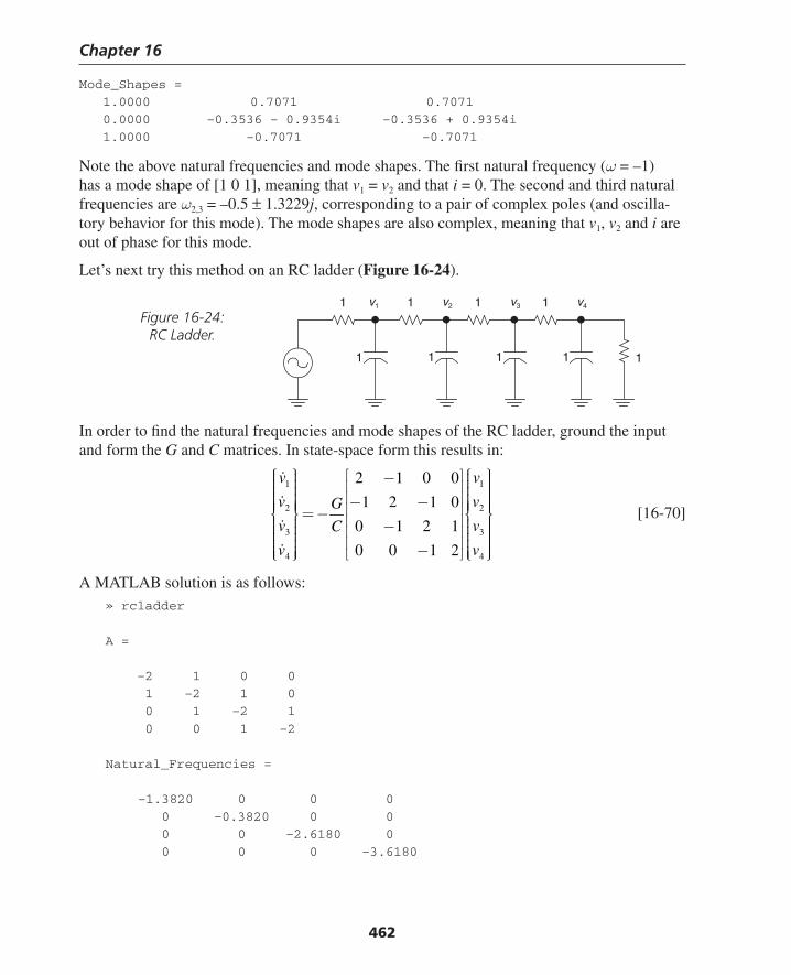
Chapter 16
462
Mode_Shapes =
1.0000 0.7071 0.7071
0.0000 –0.3536 – 0.9354i –0.3536 + 0.9354i
1.0000 –0.7071 –0.7071
Note the above natural frequencies and mode shapes. The fi rst natural frequency (ω = –1) has a mode shape of [1 0 1], meaning that v1 = v2 and that i = 0. The second and third natural frequencies are ω2,3 = –0.5 ± 1.3229j, corresponding to a pair of complex poles (and oscilla-tory behavior for this mode). The mode shapes are also complex, meaning that v1, v2 and i are out of phase for this mode.
Let’s next try this method on an RC ladder (Figure 16-24).
In order to fi nd the natural frequencies and mode shapes of the RC ladder, ground the input and form the G and C matrices. In state-space form this results in:
1 1
2 2
3 3
4 4
2 1 0 0
1 2 1 0
0 1 2 1
0 0 1 2
v v
v vG
v vC
v v
⎧ ⎫ ⎧ ⎫⎡ ⎤−⎪ ⎪ ⎪ ⎪⎪ ⎪ ⎪ ⎪⎢ ⎥⎪ ⎪ ⎪ ⎪⎢ ⎥⎪ ⎪ ⎪ ⎪− −⎪ ⎪ ⎪ ⎪⎪ ⎪ ⎪ ⎪⎢ ⎥= −⎨ ⎬ ⎨ ⎬⎢ ⎥⎪ ⎪ ⎪ ⎪−⎪ ⎪ ⎪ ⎪⎢ ⎥⎪ ⎪ ⎪ ⎪⎢ ⎥⎪ ⎪ ⎪ ⎪−⎪ ⎪ ⎪ ⎪⎣ ⎦⎪ ⎪ ⎪ ⎪⎩ ⎭ ⎩ ⎭
[16-70]
A MATLAB solution is as follows:» rcladder
A =
–2 1 0 0
1 –2 1 0
0 1 –2 1
0 0 1 –2
Natural_Frequencies =
–1.3820 0 0 0
0 –0.3820 0 0
0 0 –2.6180 0
0 0 0 –3.6180
v1 v2
1 1
v3
1
v4
1
1 1 1 1
1
Figure 16-24: RC Ladder.
Thompson Book.indb 462 3/20/2006 11:37:43 AM

Other Useful Design Techniques and Loose Ends
463
Mode_Shapes =
1.0000 –0.6180 –1.0000 –0.6180
0.6180 –1.0000 0.6180 1.0000
-0.6180 –1.0000 0.6180 –1.0000
-1.0000 –0.6180 –1.0000 0.6180
From this analysis, the lowest frequency pole is at ω = –0.38 radians/second. This pole will dominate the input-output response.
Some Comments on Scaling Laws in NatureScaling laws and dimensional analysis are very valuable tools for determining how structures, circuits and processes scale. The rationale for using scaling laws is as follows: building a full-scale prototype is often impractical and/or dangerous. An alternate strategy is to build a smaller-scale model and use scaling laws to determine how the full-scale system will behave. This method of scale-modeling is often used in:
• Aerodynamics (wind tunnel tests)
• Hydrodynamics
• Magnetic (i.e., Maglev)
• Rocketry
• Power electronics
Many interesting scaling laws can be inferred by studying simple examples in engineering and nature.
Table 16-2: List of symbols.
B Magnetic fl ux density (Tesla)Cd Aerodynamic/hydrodynamic drag coeffi cientEk Kinetic energy = ½ Mv2 (joules)fd Drag force (Newtons)l Length scaleP Power (joules, or watts/sec)v Velocity (m/sec)σ Electrical conductivity (1/Ω-m)ε Dielectric permittivity (farads/meter)µ Magnetic permeability (henry/meter)µo Magnetic permeability of free space (4π × 10–7 henry/meter)
Thompson Book.indb 463 3/20/2006 11:37:43 AM
Chapter 16
464
Geometric ScalingBy elementary mathematics, in similar fi gures the surface area scales as the square of the linear dimension and the mass scales as the cube of the linear dimension.10 In a sphere the surface area is 4πr2 while the volume is 4/3πr3 and hence the ratio of volume to surface is 1/3r. In other words, the ratio of volume to surface area scales as the length scale l.
Fish/ship speed (Froude’s law)If every length scale l is increased by the same factor, how does the speed of a ship (or a fi sh for that matter) scale? Well, the propulsion power that an engine can provide is proportional to the mass of the engine, which scales as l3, or:
31pP k l= [16-71]
The drag force on the hull is proportional to velocity. The proportionality constant is the drag constant Cd, which is proportional to hull area.
22D df C v k l v= = [16-72]
In steady state, the propulsion power balances the power due to the drag force on the hull, with power equal to force multiplied by velocity. Hence, the drag power is:
2 22D dP f v k l v= = [16-73]
In steady state the propulsion power and the drag power are equal, resulting in:
3 2 21 2k l k l v= [16-74]
Manipulating this expression results in:
2 1
2
kv l v l
k∝= ⇒ [16-75]
This result, known as Froude’s law, shows that if everything else is equal the maximum veloc-ity of a ship scales as the square root of the length scale. For example, if a 100-foot long ferry can travel at 10 mph, a scaled-up ship that is 1000 feet long will have a maximum speed of approximately 32 mph.
FruitHow do the sizes of plants scale? For instance, the stalk of a piece of fruit can withstand a maximum stress (or force per unit area) in Newtons/m2. The force exerted on the stalk scales as the mass of the fruit, or:
3f l∝ [16-76]
The area of the stalk scales as l2. Therefore, the force/area scales as l. Results from this scal-ing law are:
• Enormous structures, if scaled up directly, will collapse under their own weight.
• Old trees have huge bases.
10 This example, as well as some of the examples to follow, are derived from Darcy W. Thompson’s, On Growth and Form.
Thompson Book.indb 464 3/20/2006 11:37:43 AM
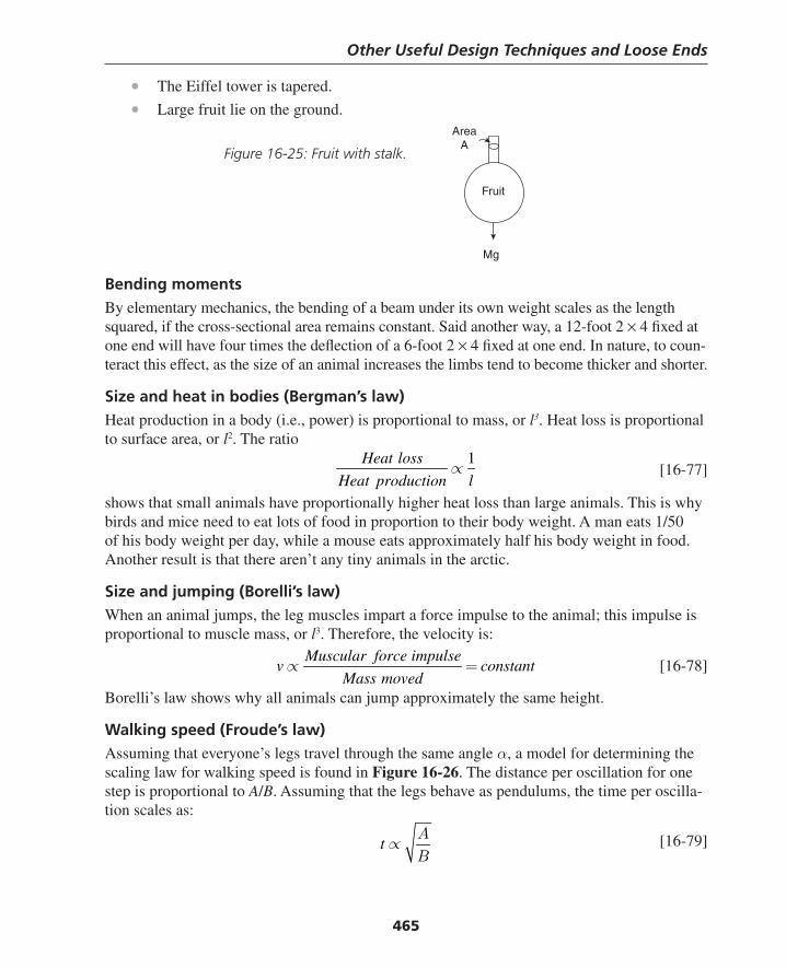
Other Useful Design Techniques and Loose Ends
465
• The Eiffel tower is tapered.
• Large fruit lie on the ground.
Bending momentsBy elementary mechanics, the bending of a beam under its own weight scales as the length squared, if the cross-sectional area remains constant. Said another way, a 12-foot 2 × 4 fi xed at one end will have four times the defl ection of a 6-foot 2 × 4 fi xed at one end. In nature, to coun-teract this effect, as the size of an animal increases the limbs tend to become thicker and shorter.
Size and heat in bodies (Bergman’s law)Heat production in a body (i.e., power) is proportional to mass, or l3. Heat loss is proportional to surface area, or l2. The ratio
1Heat loss
Heat production l∝ [16-77]
shows that small animals have proportionally higher heat loss than large animals. This is why birds and mice need to eat lots of food in proportion to their body weight. A man eats 1/50 of his body weight per day, while a mouse eats approximately half his body weight in food. Another result is that there aren’t any tiny animals in the arctic.
Size and jumping (Borelli’s law)When an animal jumps, the leg muscles impart a force impulse to the animal; this impulse is proportional to muscle mass, or l3. Therefore, the velocity is:
Muscular force impulse
v constantMass moved
∝ = [16-78]
Borelli’s law shows why all animals can jump approximately the same height.
Walking speed (Froude’s law)Assuming that everyone’s legs travel through the same angle α, a model for determining the scaling law for walking speed is found in Figure 16-26. The distance per oscillation for one step is proportional to A/B. Assuming that the legs behave as pendulums, the time per oscilla-tion scales as:
tΑ
∝Β
[16-79]
Mg
AreaA
Fruit
Figure 16-25: Fruit with stalk.
Thompson Book.indb 465 3/20/2006 11:37:44 AM
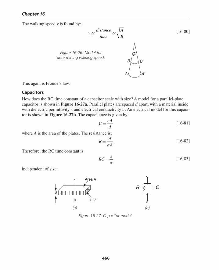
Chapter 16
466
The walking speed v is found by:
distance Av
time B∝ ∝ [16-80]
This again is Froude’s law.
CapacitorsHow does the RC time constant of a capacitor scale with size? A model for a parallel-plate capacitor is shown in Figure 16-27a. Parallel plates are spaced d apart, with a material inside with dielectric permittivity ε and electrical conductivity σ. An electrical model for this capaci-tor is shown in Figure 16-27b. The capacitance is given by:
AC
d
ε= [16-81]
where A is the area of the plates. The resistance is:
dR
Aσ= [16-82]
Therefore, the RC time constant is
RCεσ
= [16-83]
independent of size.
A
α
A'
B B'
Figure 16-26: Model for determining walking speed.
(a) (b)
Figure 16-27: Capacitor model.
Area A
d
ε, σ
CR
Thompson Book.indb 466 3/20/2006 11:37:44 AM
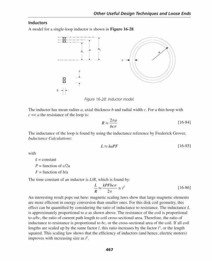
Other Useful Design Techniques and Loose Ends
467
InductorsA model for a single-loop inductor is shown in Figure 16-28.
Figure 16-28: Inductor model.
The inductor has mean radius a, axial thickness b and radial width c. For a thin hoop with c << a the resistance of the loop is:
2 aR
bc
πσ
≈ [16-84]
The inductance of the loop is found by using the inductance reference by Frederick Grover, Inductance Calculations:
L kaPF≈ [16-85]
with
k = constant
P = function of c/2a
F = function of b/a
The time constant of an inductor is L/R, which is found by:
2
2
L kPFbcl
R
σ∝
π≈ [16-86]
An interesting result pops out here: magnetic scaling laws show that large magnetic elements are more effi cient in energy conversion than smaller ones. For this disk coil geometry, this effect can be quantifi ed by considering the ratio of inductance to resistance. The inductance L is approximately proportional to a as shown above. The resistance of the coil is proportional to a/bc, the ratio of current path length to coil cross-sectional area. Therefore, the ratio of inductance to resistance is proportional to bc, or the cross-sectional area of the coil. If all coil lengths are scaled up by the same factor l, this ratio increases by the factor l2, or the length squared. This scaling law shows that the effi ciency of inductors (and hence, electric motors) improves with increasing size as l2.
b
a
c
a1
a2a
c
Thompson Book.indb 467 3/20/2006 11:37:45 AM
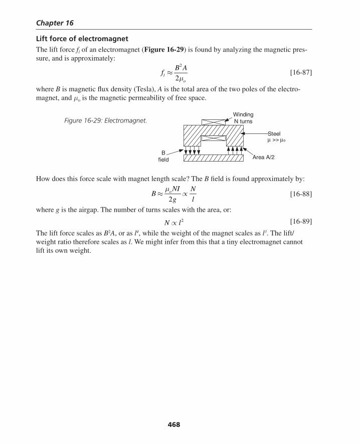
Chapter 16
468
Lift force of electromagnetThe lift force fl of an electromagnet (Figure 16-29) is found by analyzing the magnetic pres-sure, and is approximately:
2
2lo
B Af
μ≈ [16-87]
where B is magnetic fl ux density (Tesla), A is the total area of the two poles of the electro-magnet, and μo is the magnetic permeability of free space.
How does this force scale with magnet length scale? The B fi eld is found approximately by:
2oNI N
Bg l
μ∝≈ [16-88]
where g is the airgap. The number of turns scales with the area, or:
2N l∝ [16-89]
The lift force scales as B2A, or as l4, while the weight of the magnet scales as l3. The lift/weight ratio therefore scales as l. We might infer from this that a tiny electromagnet cannot lift its own weight.
Area A/2
WindingN turns
Bfield
μ >> μo
Steel
Figure 16-29: Electromagnet.
Thompson Book.indb 468 3/20/2006 11:37:45 AM
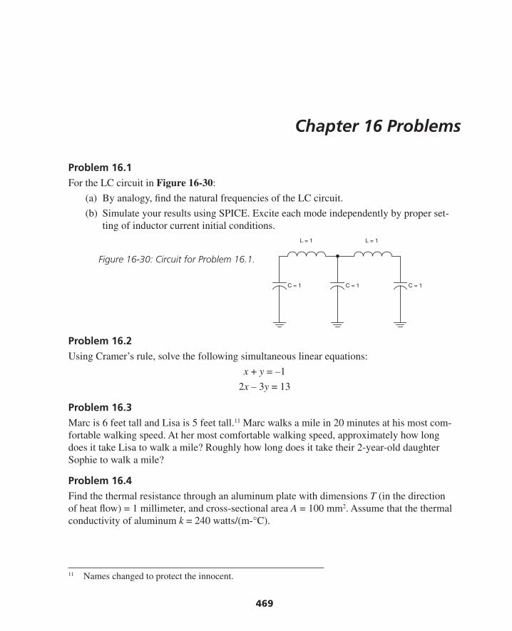
469
Chapter 16 Problems
Problem 16.1For the LC circuit in Figure 16-30:
(a) By analogy, fi nd the natural frequencies of the LC circuit.
(b) Simulate your results using SPICE. Excite each mode independently by proper set-ting of inductor current initial conditions.
Problem 16.2Using Cramer’s rule, solve the following simultaneous linear equations:
x + y = –1
2x – 3y = 13
Problem 16.3Marc is 6 feet tall and Lisa is 5 feet tall.11 Marc walks a mile in 20 minutes at his most com-fortable walking speed. At her most comfortable walking speed, approximately how long does it take Lisa to walk a mile? Roughly how long does it take their 2-year-old daughter Sophie to walk a mile?
Problem 16.4Find the thermal resistance through an aluminum plate with dimensions T (in the direction of heat fl ow) = 1 millimeter, and cross-sectional area A = 100 mm2. Assume that the thermal conductivity of aluminum k = 240 watts/(m-°C).
L = 1 L = 1
C = 1 C = 1 C = 1
Figure 16-30: Circuit for Problem 16.1.
11 Names changed to protect the innocent.
Thompson Book.indb 469 3/20/2006 11:37:46 AM
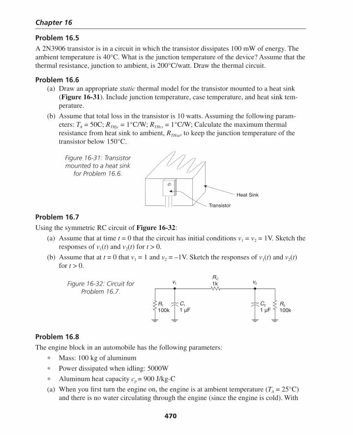
Chapter 16
470
Problem 16.5A 2N3906 transistor is in a circuit in which the transistor dissipates 100 mW of energy. The ambient temperature is 40°C. What is the junction temperature of the device? Assume that the thermal resistance, junction to ambient, is 200°C/watt. Draw the thermal circuit.
Problem 16.6(a) Draw an appropriate static thermal model for the transistor mounted to a heat sink
(Figure 16-31). Include junction temperature, case temperature, and heat sink tem-perature.
(b) Assume that total loss in the transistor is 10 watts. Assuming the following param-eters: TA = 50C; RTHjc = 1°C/W; RTHcs = 1°C/W; Calculate the maximum thermal resistance from heat sink to ambient, RTHsa, to keep the junction temperature of the transistor below 150°C.
Problem 16.7Using the symmetric RC circuit of Figure 16-32:
(a) Assume that at time t = 0 that the circuit has initial conditions v1 = v2 = 1V. Sketch the responses of v1(t) and v2(t) for t > 0.
(b) Assume that at t = 0 that v1 = 1 and v2 = –1V. Sketch the responses of v1(t) and v2(t) for t > 0.
Transistor
Heat Sink
Figure 16-31: Transistor mounted to a heat sink
for Problem 16.6.
Figure 16-32: Circuit for Problem 16.7.
v2
C2
1 µF
v1
C1
1 µFR1
100kR2
100k
RC
1k
Problem 16.8The engine block in an automobile has the following parameters:
• Mass: 100 kg of aluminum
• Power dissipated when idling: 5000W
• Aluminum heat capacity cp = 900 J/kg-C
(a) When you fi rst turn the engine on, the engine is at ambient temperature (TA = 25°C) and there is no water circulating through the engine (since the engine is cold). With
Thompson Book.indb 470 3/20/2006 11:37:46 AM
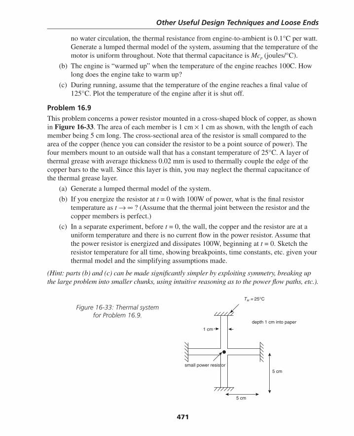
Other Useful Design Techniques and Loose Ends
471
no water circulation, the thermal resistance from engine-to-ambient is 0.1°C per watt. Generate a lumped thermal model of the system, assuming that the temperature of the motor is uniform throughout. Note that thermal capacitance is Mcp (joules/°C).
(b) The engine is “warmed up” when the temperature of the engine reaches 100C. How long does the engine take to warm up?
(c) During running, assume that the temperature of the engine reaches a fi nal value of 125°C. Plot the temperature of the engine after it is shut off.
Problem 16.9This problem concerns a power resistor mounted in a cross-shaped block of copper, as shown in Figure 16-33. The area of each member is 1 cm × 1 cm as shown, with the length of each member being 5 cm long. The cross-sectional area of the resistor is small compared to the area of the copper (hence you can consider the resistor to be a point source of power). The four members mount to an outside wall that has a constant temperature of 25°C. A layer of thermal grease with average thickness 0.02 mm is used to thermally couple the edge of the copper bars to the wall. Since this layer is thin, you may neglect the thermal capacitance of the thermal grease layer.
(a) Generate a lumped thermal model of the system.
(b) If you energize the resistor at t = 0 with 100W of power, what is the fi nal resistor temperature as t → ∞ ? (Assume that the thermal joint between the resistor and the copper members is perfect.)
(c) In a separate experiment, before t = 0, the wall, the copper and the resistor are at a uniform temperature and there is no current fl ow in the power resistor. Assume that the power resistor is energized and dissipates 100W, beginning at t = 0. Sketch the resistor temperature for all time, showing breakpoints, time constants, etc. given your thermal model and the simplifying assumptions made.
(Hint: parts (b) and (c) can be made signifi cantly simpler by exploiting symmetry, breaking up the large problem into smaller chunks, using intuitive reasoning as to the power fl ow paths, etc.).
Figure 16-33: Thermal system for Problem 16.9.
TW = 25°C
depth 1 cm into paper
5 cm
5 cm
1 cm
small power resistor
Thompson Book.indb 471 3/20/2006 11:37:47 AM
Chapter 16
472
ReferencesFogel, M., Editor, The Automatic Control Systems/Robotics Problem Solver, Research and
Education Association, Piscataway NJ, 1990.General Electric Corp., SCR Handbook, 6th Edition. Good general-purpose manual with lots
of practical advice on heat sink design, and mounting and cooling techniques for power devices.
Gilbert, B., “A New Wide-Band Amplifi er Technique,” IEEE Journal of Solid State Circuits, vol. SC-3, no. 4, December 1968, pp. 353–365.
———, “A Precise Four-Quadrant Multiplier with Subnanosecond Response,” IEEE Journal of Solid State Circuits, vol. SC-3, no. 4, December 1968, pp. 365–373.
———, “A DC-500 MHz Amplifi er Multiplier Principle,” 1968 ISSCC Digest of Technical Papers, pp. 114–115.
———, “Translinear Circuits: A Proposed Classifi cation,” Electronics Letters, vol. , no. 1, pp. 14–16, 1975.
———, “Current-Mode Circuits from a Translinear Viewpoint: A Tutorial,” in C. Toumazou, F. J. Lidgey, and D. G. Haigh, eds., Analogue IC Design: The Current-Mode Approach, London: Peter Peregrinus, pp. 11–91, 1990.
———, “Translinear Circuits—25 Years On, Part I: The Foundations,” Electronic Engineering, vol. 65, no. 800, pp. 21–24, 1993.
———, “Translinear Circuits: An Historical Review,” Analog Integrated Circuits and Signal Processing, vol. 9, no. 2, pp. 95–118, 1996.
Grover, F., Inductance Calculations, originally published by D. Van Nostrand, 1946, reprinted by Dover, 2004.
Jezierski, E., “On Electrical Analogues of Mechatronic Systems,” Proceedings of the 2001 Sec-ond International Workshop on Motion and Control, October 18–20, 2001, pp. 181–188.
Kassakian, J., Schlecht, M., and Verghese, G., Principles of Power Electronics, Prentice-Hall, 1991. A well-regarded reference for all aspects of power electronics design, including magnetics.
Klein, Richard E., “Teaching Linear Systems Theory Using Cramer’s Rule,” IEEE Transac-tions on Education, vol. 33, no. 3, August 1990, pp. 258–267.
Langlois, P. J., “Graphical Analysis of Delay Line Waveforms: A Tutorial,” IEEE Transac-tions on Education, vol. 38, no. 1, February 1995, pp. 27–32.
Mathworks, Inc., MATLAB Reference Guide, 1992.Middlebrook, R. D., “Null Double Injection and the Extra Element Theorem,” IEEE Transac-
tions on Education, vol. 32, no. 3, August 1989, pp. 167–180. ———, “The Two Extra Element Theorem,” Proceedings of the IEEE Frontiers in Educa-
tion Twenty-First Annual Conference, Purdue University, September 21–24, 1991, pp. 702–708.
———, “Low-Entropy Expressions: The Key to Design-Oriented Analysis,” Proceedings of the IEEE Frontiers in Education Twenty-First Annual Conference, Purdue University, September 21–24, 1991, pp. 399–403.
Thompson Book.indb 472 3/20/2006 11:37:47 AM

Other Useful Design Techniques and Loose Ends
473
Rao, Singiresu S., Mechanical Vibrations, 3d edition, Addison-Wesley, 1995.Rothkopf, Elliot, “Teaching for Understanding—Analogies for Learning in Electrical Engi-
neering,” 1995 IEEE Frontiers in Education Conference, session 2b4, pp. 2b4.9–2b4.13.Seevinck, E., and Wiegerink, R. J., “Generalized translinear circuit principle,” IEEE Journal
of Solid-State Circuits, Volume 26, no. 8 , August 1991, pp. 1098–1102.Shen, Liang Chi, and Kong, Jin Au, Applied Electromagnetism, Brooks/Cole, 1983.Teoh, Chin Soon, and Davis, Lionel E., “A Coupled Pendula System as an Analogy to Cou-
pled Transmission Lines,” IEEE Transactions on Education, vol. 39, no. 4, November 1996, pp. 548–557.
Thompson, D’Arcy W., On Growth and Form, Dover Publications (reprinted), 1992. Thornton, Richard D., Electronic Circuits Modeling, Analysis, Simulation; Intuition and De-
sign, MIT course notes, January 1993.Vorperian, Vatche, “Improved Circuit-Analysis Techniques Require Minimum Algebra,”
EDN, August 3, 1995, pp. 125–134.Zahn, Markus, Electromagnetic Field Theory: A Problem Solving Approach, reprinted by
Krieger, 1987.
Thompson Book.indb 473 3/20/2006 11:37:47 AM

Thompson Book.indb 474 3/20/2006 11:37:47 AM
475
Index
AAcceptors 53–55Amplifi ers Amplifi er, cascode 146–147, 191, 251, 355 Amplifi er, common-base 141, 191–194 Amplifi er, common-emitter 101–106, 118,
122, 132–135, 139, 142, 146, 157–158, 165, 186–188, 202, 207–208, 212, 228–229, 457
Amplifi er, common-emitter with emitter degeneration 165–167, 203, 358
Amplifi er, current 194 Amplifi er, differential 112–118, 139–140,
167–168, 248, 348, 355, 361–362 Amplifi er, high-gain 225, 227, 229, 231,
233–234, 236 Amplifi er, logarithmic 6–7 Amplifi er, MOS 241, 248, 255–256, 258,
261, 264–265 Amplifi er, peaking 118, 190–191 Amplifi er, photodiode 327–330 Amplifi er, push-pull 351, 358 Amplifi er, video 203, 344, 379Analogies Mechanical circuits 117, 444–448 hermal circuits 440–448
BBiasing 97–125Bode plot 36–37, 142, 175, 185, 314, 316–318,
320, 323–324, 326, 332, 375, 390Bardeen, John 3, 43, 75
Base spreading resistance 86, 92–93, 101, 143, 187, 190, 236, 290, 373
Base-width modulation 207–211, 246, 373Beta 78, 84, 88, 90, 220–221, 358Biasing, transistor 97Black, Harold 306–308Bootstrapping 165, 177–183Brattain, Walter 3, 75
CCapacitance Capacitance, diffusion 63, 65–66, 85 Capacitance, junction 63–64, 85–86, 91–
93, 274–276, 278–279, 282, 290Capacitors Parasitic elements 421, 424, 436 ESR 422, 436Cascaded systems 37 Cascode 146, 150, 153, 191, 214–215, 222,
251, 254, 262, 355Charge control model 269–303Characteristic impedance 25, 34–35, 418, 448,
452Common mode 115–118Common-source amplifi er 249–251, 255 Conductive heat transfer 440Conductor 43–45Cramer’s rule 103, 111, 197, 455–458Crossover distortion 348–349, 351Crossover frequency 314, 316–317, 321–322,
325–326, 328, 330, 332 Current density 46, 61–62
Thompson Book.indb 475 3/20/2006 11:37:48 AM

Index
476
Current feedback 369–381Current feedback op-amps 5, 194, 369–381 Absence of slew rate limiting 375 Basic current feedback op-amp 369, 372 LM6181 379–380 Current-feedback op-amp limitations 5,
369, 381 Current mirror 218–237, 352–354, 358, 372–
373, 376, 379 Basic current mirror 218–219 Cascode current mirror 222 Current mirror with “beta helper” 220 Current mirror with emitter
degeneration 219 MOS current mirrors 252–254 Wilson current mirror 221, 252–254 Widlar current mirror 222–224Current repeater 218Current source 15, 72, 108, 110, 114–117, 133,
136, 144, 161, 164, 171, 174, 208, 210, 212–215, 219, 224–225, 228, 230–231, 250–252, 258, 278, 327, 331–334, 352, 355, 358, 376, 379, 425, 429–430, 442, 444
Current source, incremental output resistance 115, 208, 212–213, 224–225, 231, 250, 253, 348
MOSFET current source 331–334, 340Current switching 194–196, 292, 431–432Current gain 75–76, 78, 84, 86–91, 97–98,
100–101, 109, 133, 139, 146, 165, 169, 187, 211–212, 216, 219–220, 228, 295–297, 372
DDamping ratio 25–30, 315, 321, 324, 337Datasheet Datasheet, diode 67–69 Datasheet, fi nding parameters on 211–212 Datasheet h-parameters 211–212 Datasheet, transistor 84, 88–93, 211–212Depletion region 54–63, 65–67, 71, 89, 210,
246, 282, 287Depletion capacitance 63–64, 85, 91, 247, 274,
287
Desensitivity in feedback systems 309Differential mode 112, 114–116, 118, 139–
140, 167, 194, 348, 362Diffusion 48, 52, 54–57, 59–63, 65–67, 77, 85,
270 Diffusion constants 50–51, 62Diode Ideal diode equation 62–63 In thermal equilibrium 54–57, 77 Forward-biased 57–58, 60, 77–79, 81, 282 Reverse-biased 61, 66, 77–80, 271 Schottky 70Disturbance rejection in feedback systems 309Donors 53–55, 59Doping 43, 48, 52–56, 59, 276Drift 48–52, 54, 56–57, 77, 360–361
EEarly effect 224Electrical conductivity 43–44, 242, 421, 440,
463, 466 Electron 44–54, 59–61, 65–66, 77Electron current 60–61Emitter degeneration 165–168, 219–220, 224,
358Emitter follower 107–112, 117, 136–139, 150,
153, 215–217, 228, 230–233, 248, 263, 265, 348, 355
Input and output impedance 107–110, 168–176, 215
Energy method 34–35, 41
FFeedback systems 305–344 Crossover frequency 314, 316–317, 321–
322, 325–326, 328, 330, 372 Desensitivity 309 History of feedback control 305 Loop transmission 309, 314, 316–318,
320–322, 325–326, 328, 332–333 Phase margin and gain margin 314–315,
317, 321–323, 325–326, 332–333 Routh stability criterion 311, 319
Thompson Book.indb 476 3/20/2006 11:37:48 AM

Index
477
Stability 310–311, 314, 319, 328, 330Fick’s law 49Filters All-pass 406–407 Bessel 395–401 “Brick wall” fi lter 404–405 Butterworth 387–389 Chebyshev 390–395 Comparison of different fi lter types 398–
399 Elliptic 404–405, 408 Group delay 385–390, 394–396, 398–399,
404, 406–408, 410–413 Implementation 400, 404 Ladder 400, 403, 408–413 Passband 386–387, 390–396, 398, 402,
404, 408, 410–411 Sallen-Key 387, 404, 406, 408 Stopband 386, 398, 404, 410 Transition band 388, 390, 395, 405Full-wave rectifi er 20–21Fusing current 426–427
GGain-bandwidth product 5, 86–87, 139, 297,
332, 347, 369–371, 375, 378, 411 Gain margin 314–315, 317, 326Generation 48, 52, 54, 78Group delay 18–19, 385–390, 394–396, 398–
399, 404, 406–408, 410–413Grover, Frederick W., 428, 467
HHole 45–62, 65–67, 77–79, 270Hole current 46, 60–61Hybrid-pi model 207, 209–212, 215, 222, 269,
274 Extended hybrid-pi model 210–212, 215,
222 Hybrid-pi model, limitations 93
IIncremental model 82, 84–87, 165, 169, 171,
173–174, 207–208, 215, 226, 252–253Inductors 2, 7, 14–15, 23, 34, 400, 408, 424,
444, 447, 452, 467 Nonideal 424Insulator 43–45, 441 Intrinsic carrier 47, 59, 71Intrinsic carrier concentration 47, 59, 71
KKilby, J., and invention of the integrated
circuit 4
LLag network 316Laplace transform 9, 13 Laser diode driver 428Lead network 317Lilienfeld, Julius 2–3, 241Load line 43, 71–72, 80, 97–98Loop transmission 309, 314, 316–318, 320–
322, 325–326, 328, 332–333Low-pass fi lters 385–415
MMaglev 334, 336–337, 341, 463Mass-spring system 23–24, 273MATLAB xii, 33, 104, 132, 321, 326, 338,
340–341, 392, 459–462Miller effect 105–107, 145–147, 177, 194, 251,
262, 372Minority carriers 51, 59–60, 270 Minority carrier concentration 59, 61, 65,
85, 210, 270, 276 MOSFET “Back-gate” effect 247–251, 255 Basic MOS devices 241–267 Early history 241 V/I curve 243–246 Small-signal model 246–247, 255–256,
258–259, 262–263
Thompson Book.indb 477 3/20/2006 11:37:48 AM

Index
478
NNatural frequency 25–28, 30, 444, 446–447,
458, 460Node equations 455–457Nonsaturating current switch 290
OOpen-circuit time constants 127–155 Worst case calculation 161–165Operational amplifi er 4 Bias current 362 Capacitive loading 363–365 Common-mode rejection ratio
(CMRR) 117 Current-feedback op-amps 369–381 Gain-bandwidth product 369–371, 375,
378 Output resistance 363 Slew rate 362–363, 371, 375 Voltage offset 359–360 Voltage offset drift 360–361 741 op-amp 358Oscillation modes 458–463
PPC boards, (see printed-circuit boards) Phase margin 314–315, 321–326, 365Pole/zero plot 36–37Pole splitting 196–197, 199–200, 348, 358, 362Printed-circuit boards 425–427 Design case study 428–435 Ground planes 426 Layout issues 425–427 Power supply bypassing 425 Trace widths 426
QQ (see “quality factor”) Quality factor 27–28
RRecombination 48, 52, 54, 89, 280–281, 286Resonance 27–28, 33–35, 430Resistors 417 Parasitic elements 417–419 Surface-mount resistors 419–420 Temperature coeffi cients 420–421Resistive ladder 451Reverse breakdown 66–68Reverse recovery 65–70Risetime 16–17, 22, 30, 37, 277, 287, 289,
320–322, 325, 334, 378, 430–435Routh stability criterion 311, 319
SSaturation 272–273, 289Saturation delay 286Scaling laws 463, 467Second-order systems 23–32, 129, 198, 310–
311, 315Semiconductor 43–54Shockley, William 3, 43, 45, 51–52, 62, 75–76Short-circuit time constants 142, 184–190, 228Silicon lattice 45–47, 55Source follower 248–249, 257–260, 264–265,
331 Step response 19–30
TThermal circuits 439–444Thermal equilibrium 54–57, 77Transfer function 36–37, 87, 104, 111, 119,
127–129, 135, 138, 184–186, 190, 199–200, 221, 250, 273, 308–310, 312–313, 316–317, 319–337, 363, 367, 369, 387–388, 390, 392–393, 397–398, 407, 430, 455, 457–458
Transistor Transistor, biasing 97–101 Transistor, cutoff region 79, 282–284
Thompson Book.indb 478 3/20/2006 11:37:48 AM

Index
479
Transistor, forward-active 270–272, 278, 281, 283–284, 287
Transistor inverter 277–289 Transistor, point contact 75–76 Reverse-active 271–272 Transistor, saturation region 272–273 Transistor datasheet 211–212Transistor switching 269–303 Emitter switching 292–293 Inverter 277–289
Nonsaturating current switch 290–291 Translinear principle 449–450Transmission lines 451–455
WWidlar, Robert 5–6Widely-spaced pole approximation 185, 273
ZZo (see “characteristic impedance”)
Thompson Book.indb 479 3/20/2006 11:37:48 AM

480
What’s on the CD-ROM?
Included on the CD-ROM are Powerpoint presentations for each chapter, suitable for use by instructors. Also included are selected MATLAB scripts which were used in preparation of the text.
Thompson Book.indb 480 3/20/2006 11:37:48 AM

ELSEVIER SCIENCE CD-ROM LICENSE AGREEMENT
PLEASE READ THE FOLLOWING AGREEMENT CAREFULLY BEFORE USING THIS CD-ROM PRODUCT. THIS CD-ROM PRODUCT IS LICENSED UNDER THE TERMS CONTAINED IN THIS CD-ROM LICENSE AGREEMENT (“Agreement”). BY USING THIS CD-ROM PRODUCT, YOU, AN INDIVIDUAL OR ENTITY INCLUDING EMPLOYEES, AGENTS AND REPRESENTATIVES (“You” or “Your”), ACKNOWLEDGE THAT YOU HAVE READ THIS AGREEMENT, THAT YOU UN-DERSTAND IT, AND THAT YOU AGREE TO BE BOUND BY THE TERMS AND CONDITIONS OF THIS AGREEMENT. ELSEVIER SCIENCE INC. (“Elsevier Science”) EXPRESSLY DOES NOT AGREE TO LICENSE THIS CD-ROM PRODUCT TO YOU UNLESS YOU ASSENT TO THIS AGREEMENT. IF YOU DO NOT AGREE WITH ANY OF THE FOLLOWING TERMS, YOU MAY, WITHIN THIRTY (30) DAYS AFTER YOUR RECEIPT OF THIS CD-ROM PRODUCT RETURN THE UNUSED CD-ROM PRODUCT AND ALL ACCOMPANYING DOCUMENTATION TO ELSEVIER SCIENCE FOR A FULL REFUND.
DEFINITIONS
As used in this Agreement, these terms shall have the following meanings:
“Proprietary Material” means the valuable and proprietary information content of this CD-ROM Product including all indexes and graphic materials and software used to access, index, search and retrieve the information content from this CD-ROM Product developed or licensed by Elsevier Science and/or its affi liates, suppliers and licensors.
“CD-ROM Product” means the copy of the Proprietary Material and any other material delivered on CD-ROM and any other hu-man-readable or machine-readable materials enclosed with this Agreement, including without limitation documentation relating to the same.
OWNERSHIP
This CD-ROM Product has been supplied by and is proprietary to Elsevier Science and/or its affi liates, suppliers and licensors. The copyright in the CD-ROM Product belongs to Elsevier Science and/or its affi liates, suppliers and licensors and is protected by the national and state copyright, trademark, trade secret and other intellectual property laws of the United States and international treaty provisions, including without limitation the Universal Copyright Convention and the Berne Copyright Convention. You have no ownership rights in this CD-ROM Product. Except as expressly set forth herein, no part of this CD-ROM Product, including without limitation the Proprietary Material, may be modifi ed, copied or distributed in hardcopy or machine-readable form without prior written consent from Elsevier Science. All rights not expressly granted to You herein are expressly reserved. Any other use of this CD-ROM Product by any person or entity is strictly prohibited and a violation of this Agreement.
SCOPE OF RIGHTS LICENSED (PERMITTED USES)
Elsevier Science is granting to You a limited, non-exclusive, non-transferable license to use this CD-ROM Product in accordance with the terms of this Agreement. You may use or provide access to this CD-ROM Product on a single computer or terminal physi-cally located at Your premises and in a secure network or move this CD-ROM Product to and use it on another single computer or terminal at the same location for personal use only, but under no circumstances may You use or provide access to any part or parts of this CD-ROM Product on more than one computer or terminal simultaneously.
You shall not (a) copy, download, or otherwise reproduce the CD-ROM Product in any medium, including, without limitation, online transmissions, local area networks, wide area networks, intranets, extranets and the Internet, or in any way, in whole or in part, except that You may print or download limited portions of the Proprietary Material that are the results of discrete searches; (b) alter, modify, or adapt the CD-ROM Product, including but not limited to decompiling, disassembling, reverse engineering, or creating derivative works, without the prior written approval of Elsevier Science; (c) sell, license or otherwise distribute to third parties the CD-ROM Product or any part or parts thereof; or (d) alter, remove, obscure or obstruct the display of any copyright, trademark or other proprietary notice on or in the CD-ROM Product or on any printout or download of portions of the Proprietary Materials.
RESTRICTIONS ON TRANSFER
This License is personal to You, and neither Your rights hereunder nor the tangible embodiments of this CD-ROM Product, including without limitation the Proprietary Material, may be sold, assigned, transferred or sub-licensed to any other person, including without limitation by operation of law, without the prior written consent of Elsevier Science. Any purported sale, assignment, transfer or sublicense without the prior written consent of Elsevier Science will be void and will automatically terminate the License granted hereunder.
Thompson Book.indb 481 3/20/2006 11:37:48 AM

TERM
This Agreement will remain in effect until terminated pursuant to the terms of this Agreement. You may terminate this Agree-ment at any time by removing from Your system and destroying the CD-ROM Product. Unauthorized copying of the CD-ROM Product, including without limitation, the Proprietary Material and documentation, or otherwise failing to comply with the terms and conditions of this Agreement shall result in automatic termination of this license and will make available to Elsevier Science legal remedies. Upon termination of this Agreement, the license granted herein will terminate and You must immediately destroy the CD-ROM Product and accompanying documentation. All provisions relating to proprietary rights shall survive termination of this Agreement.
LIMITED WARRANTY AND LIMITATION OF LIABILITY
NEITHER ELSEVIER SCIENCE NOR ITS LICENSORS REPRESENT OR WARRANT THAT THE INFORMATION CON-TAINED IN THE PROPRIETARY MATERIALS IS COMPLETE OR FREE FROM ERROR, AND NEITHER ASSUMES, AND BOTH EXPRESSLY DISCLAIM, ANY LIABILITY TO ANY PERSON FOR ANY LOSS OR DAMAGE CAUSED BY ERRORS OR OMISSIONS IN THE PROPRIETARY MATERIAL, WHETHER SUCH ERRORS OR OMISSIONS RESULT FROM NEG-LIGENCE, ACCIDENT, OR ANY OTHER CAUSE. IN ADDITION, NEITHER ELSEVIER SCIENCE NOR ITS LICENSORS MAKE ANY REPRESENTATIONS OR WARRANTIES, EITHER EXPRESS OR IMPLIED, REGARDING THE PERFORMANCE OF YOUR NETWORK OR COMPUTER SYSTEM WHEN USED IN CONJUNCTION WITH THE CD-ROM PRODUCT.
If this CD-ROM Product is defective, Elsevier Science will replace it at no charge if the defective CD-ROM Product is returned to Elsevier Science within sixty (60) days (or the greatest period allowable by applicable law) from the date of shipment.
Elsevier Science warrants that the software embodied in this CD-ROM Product will perform in substantial compliance with the documentation supplied in this CD-ROM Product. If You report signifi cant defect in performance in writing to Elsevier Science, and Elsevier Science is not able to correct same within sixty (60) days after its receipt of Your notifi cation, You may return this CD-ROM Product, including all copies and documentation, to Elsevier Science and Elsevier Science will refund Your money.
YOU UNDERSTAND THAT, EXCEPT FOR THE 60-DAY LIMITED WARRANTY RECITED ABOVE, ELSEVIER SCIENCE, ITS AFFILIATES, LICENSORS, SUPPLIERS AND AGENTS, MAKE NO WARRANTIES, EXPRESSED OR IMPLIED, WITH RESPECT TO THE CD-ROM PRODUCT, INCLUDING, WITHOUT LIMITATION THE PROPRIETARY MATERIAL, AN SPECIFICALLY DISCLAIM ANY WARRANTY OF MERCHANTABILITY OR FITNESS FOR A PARTICULAR PURPOSE.
If the information provided on this CD-ROM contains medical or health sciences information, it is intended for professional use within the medical fi eld. Information about medical treatment or drug dosages is intended strictly for professional use, and because of rapid advances in the medical sciences, independent verifi cation of diagnosis and drug dosages should be made.
IN NO EVENT WILL ELSEVIER SCIENCE, ITS AFFILIATES, LICENSORS, SUPPLIERS OR AGENTS, BE LIABLE TO YOU FOR ANY DAMAGES, INCLUDING, WITHOUT LIMITATION, ANY LOST PROFITS, LOST SAVINGS OR OTHER INCIDENTAL OR CONSEQUENTIAL DAMAGES, ARISING OUT OF YOUR USE OR INABILITY TO USE THE CD-ROM PRODUCT REGARDLESS OF WHETHER SUCH DAMAGES ARE FORESEEABLE OR WHETHER SUCH DAMAGES ARE DEEMED TO RESULT FROM THE FAILURE OR INADEQUACY OF ANY EXCLUSIVE OR OTHER REMEDY.
U.S. GOVERNMENT RESTRICTED RIGHTS
The CD-ROM Product and documentation are provided with restricted rights. Use, duplication or disclosure by the U.S. Govern-ment is subject to restrictions as set forth in subparagraphs (a) through (d) of the Commercial Computer Restricted Rights clause at FAR 52.22719 or in subparagraph (c)(1)(ii) of the Rights in Technical Data and Computer Software clause at DFARS 252.2277013, or at 252.2117015, as applicable. Contractor/Manufacturer is Elsevier Science Inc., 655 Avenue of the Americas, New York, NY 10010-5107 USA.
GOVERNING LAW
This Agreement shall be governed by the laws of the State of New York, USA. In any dispute arising out of this Agreement, you and Elsevier Science each consent to the exclusive personal jurisdiction and venue in the state and federal courts within New York County, New York, USA.
Thompson Book.indb 482 3/20/2006 11:37:49 AM