Analog Communication Lab Manual , Prepared by Nakka. Ravi...
79
Analog Communication Lab Manual , Prepared by Nakka. Ravi Kumar Asst. Prof. & Roopalakshmi Asst. Prof MIST MIST, Hyderabad – ECE Department Page 1 INDEX Page No. 1. Introduction 4 2. List of experiments 4 3. General guidelines for conducting an experiment 5 3.1 Simulation 3.2 Hardware 3.3 Do’s and Don’ts 4. Experiments 6 4.1 Amplitude modulation and demodulation 7-12 4.1.1 AIM 4.1.2 Theory 4.1.3 MATLAB program and description 4.1.4 Hardware - Apparatus - Circuit diagram - Procedure - Expected waveform 4.2 DSB-SC modulation and demodulation 13-16 4.2.1 AIM 4.2.2 Theory 4.2.3 MATLAB program and description 4.2.4 Hardware - Apparatus - Circuit diagram - Procedure - Expected waveform 4.3 SSB-SC modulation and Demodulation (Phase Shift method) 17-24 4.3.1 AIM 4.3.2 Theory 4.3.3 MATLAB program and description 4.3.4 Hardware - Apparatus - Circuit diagram - Procedure - Expected waveform 4.4 Frequency modulation and demodulation 25-29 4.4.1 AIM 4.4.2 Theory 4.4.3 MATLAB program and description 4.4.4 Hardware - Apparatus - Circuit diagram - Procedure - Expected waveform 4.5 Study of spectrum analyzer and study of AM and FM signals 30-32 4.5.1 AIM 4.5.2 Theory 4.5.3 MATLAB program and description
Transcript of Analog Communication Lab Manual , Prepared by Nakka. Ravi...

Analog Communication Lab Manual , Prepared by Nakka. Ravi Kumar Asst. Prof. & Roopalakshmi Asst. Prof MIST
MIST, Hyderabad – ECE Department Page 1
INDEX
Page No.
1. Introduction 4
2. List of experiments 4
3. General guidelines for conducting an experiment 5
3.1 Simulation
3.2 Hardware
3.3 Do’s and Don’ts
4. Experiments 6
4.1 Amplitude modulation and demodulation 7-12
4.1.1 AIM
4.1.2 Theory
4.1.3 MATLAB program and description
4.1.4 Hardware
- Apparatus
- Circuit diagram
- Procedure
- Expected waveform
4.2 DSB-SC modulation and demodulation 13-16
4.2.1 AIM
4.2.2 Theory
4.2.3 MATLAB program and description
4.2.4 Hardware
- Apparatus
- Circuit diagram
- Procedure
- Expected waveform
4.3 SSB-SC modulation and Demodulation (Phase Shift method) 17-24
4.3.1 AIM
4.3.2 Theory
4.3.3 MATLAB program and description
4.3.4 Hardware
- Apparatus
- Circuit diagram
- Procedure
- Expected waveform
4.4 Frequency modulation and demodulation 25-29
4.4.1 AIM
4.4.2 Theory
4.4.3 MATLAB program and description
4.4.4 Hardware
- Apparatus
- Circuit diagram
- Procedure
- Expected waveform
4.5 Study of spectrum analyzer and study of AM and FM signals 30-32
4.5.1 AIM
4.5.2 Theory
4.5.3 MATLAB program and description
Analog Communication Lab Manual , Prepared by Nakka. Ravi Kumar Asst. Prof. & Roopalakshmi Asst. Prof MIST
MIST, Hyderabad – ECE Department Page 2
4.5.4 Hardware
- Apparatus
- Circuit diagram
- Procedure
- Expected waveform
4.6 Pre-emphasis and De-emphasis 33-36
4.6.1 AIM
4.6.2 Theory
4.6.3 MATLAB program and description
4.6.4 Hardware
- Apparatus
- Circuit diagram
- Procedure
- Expected waveform
4.7 Time division multiplexing and de-multiplexing 37-40
4.7.1 AIM
4.7.2 Theory
4.7.3 MATLAB program and description
4.7.4 Hardware
- Apparatus
- Circuit diagram
- Procedure
- Expected waveform
4.8 Frequency division multiplexing and de-multiplexing 41-47
4.8.1 AIM
4.8.2 Theory
4.8.3 MATLAB program and description
4.8.4 Hardware
- Apparatus
- Circuit diagram
- Procedure
- Expected waveform
4.9 Verification of sampling theorem 48-51
4.9.1 AIM
4.9.2 Theory
4.9.3 MATLAB program and description
4.9.4 Hardware
- Apparatus
- Circuit diagram
- Procedure
- Expected waveform
4.10 Pulse Amplitude modulation and demodulation 52-56
4.10.1 AIM
4.10.2 Theory
4.10.3 MATLAB program and description
4.10.4 Hardware
- Apparatus
- Circuit diagram
- Procedure
- Expected waveform

Analog Communication Lab Manual , Prepared by Nakka. Ravi Kumar Asst. Prof. & Roopalakshmi Asst. Prof MIST
MIST, Hyderabad – ECE Department Page 3
4.11 Pulse width modulation and demodulation 57-60
4.11.1 AIM
4.11.2 Theory
4.11.3 MATLAB program and description
4.11.4 Hardware
- Apparatus
- Circuit diagram
- Procedure
- Expected waveform
4.12 Pulse position modulation and demodulation 61-64
4.12.1 AIM
4.12.2 Theory
4.12.3 MATLAB program and description
4.12.4 Hardware
- Apparatus
- Circuit diagram
- Procedure
- Expected waveform
4.13 Frequency synthesizer 65-68
4.13.1 AIM
4.13.2 Theory
4.13.3 MATLAB program and description
4.13.4 Hardware
- Apparatus
- Circuit diagram
- Procedure
- Expected waveform
4.14 AGC characteristics 69-73
4.14.1 AIM
4.14.2 Theory
4.14.3 MATLAB program and description
4.14.4 Hardware
- Apparatus
- Circuit diagram
- Procedure
- Expected waveform
4.15 PLL and FM demodulator 74-79
4.15.1 AIM
4.15.2 Theory
4.15.3 MATLAB program and description
4.15.4 Hardware
- Apparatus
- Circuit diagram
- Procedure
- Expected waveform
Analog Communication Lab Manual , Prepared by Nakka. Ravi Kumar Asst. Prof. & Roopalakshmi Asst. Prof MIST
MIST, Hyderabad – ECE Department Page 4
1. Introduction Analog communications lab is for B.Tech III year ECE I semester. The students
learn Analog Communications theory subject in the same semester. The lab experiments are
meant to equip the students with firm practical knowledge of the concerned subject. As listed
in section-2, there are total fifteen (15) experiments in this lab which are according to JNTUH
R-13 syllabus, out of which minimum 12 experiments are to be conducted
General procedure for conducting an experiment is described in Section – 3. Each
experiment will first be simulated using MATLAB, a simulation software program, which the
students have already learned in Basic Simulation lab in II year I semester. The same
experiment will then be realized using proper hardware, as described in detail for each
experiment in section -4.
2. List of Experiments
1. Amplitude modulation and demodulation
2. DSB-SC modulator and detector
3. SSB-SC modulator and detector
4. Frequency modulation and demodulation
5. Study of Spectrum Analyzer and Analysis of AM and FM Signals
6. Pre-emphasis and de-emphasis
7. Time division multiplexing and de-multiplexing
8. Frequency division multiplexing and de-multiplexing
9. Verification of sampling theorem
10. Pulse amplitude modulation and demodulation
11. Pulse width modulation and demodulation
12. Pulse Position modulation and demodulation
13. Frequency synthesizer
14. AGC Characteristics
15. PLL & FM demodulator
Analog Communication Lab Manual , Prepared by Nakka. Ravi Kumar Asst. Prof. & Roopalakshmi Asst. Prof MIST
MIST, Hyderabad – ECE Department Page 5
3.0 General Guidelines for conducting an experiment Each experiment first has to be simulated using MATLAB and then be realized in hardware as
described in Section -4.
MATLAB, short for MATrix LABoratory is a programming package specifically designed for
scientific calculations and I/O. It has literally hundreds of built-in functions for a wide variety of
computations and many tool boxes designed for specific research disciplines, including statistics,
optimization, solution of partial differential equations and data analysis.
3.1 Simulation
Each experiment will first be simulated with MATLAB software package. The MATLAB
program code for each experiment is given in the following section. The students have to write the
programs in PC and execute them using MATLAB software and make sure that they get the expected
waveforms as shown in this manual.
The students are also advised to change certain parameters in the MATLAB program and see
their impact on the output waveforms.
3.2 Hardware
After completion of the simulation, each experiment has to be realized in hardware as
described for all experiments in section – 4. Out of fifteen experiments, fourteen experiments are to be
conducted with the PHYSITECH lab kits along with the additional instruments as mentioned for each
experiment in section – 4. The fifth experiment, “Study of Spectrum Analyzer and Analysis of AM
and FM Signals” does not require the PHYSIITECH experiment kit.
3.3 Do’s and Don’ts
The students are to follow the given general Do’s and Don’ts for simulation lab.
Do’s:
1. Enter in to the simulation lab in time.
2. Wear student identity badges round your neck before entering the lab.
3. Keep silence in the lab
4. Follow the instructions of the lab in-charges and lab supervisor.
5. Always save your input files and results in the prescribed directory.
Don’ts:
1. Do not use internet or open any other programs other than MATLAB.
2. Do not mishandle or rough handle the keyboard of CPU.
3. Do not use pen drive or card reader without the permission of the lab in-charge.
4. Do not make noise in the lab.
The students are to follow the given general Do’s and Don’ts for hardware lab
Do’s
1. Enter the hardware lab in time.
2. Wear shoes/sandals in the lab.
3. Wear student identity badge before entering the lab
4. Follow the instructions of the lab in-charges and lab supervisor.
Don’ts: 1. Do not make noise in the lab.
2. Do not switch the power supply until you finish all the connections.
3. Do not remove connecting wires or probes when the power is ON.
4. Do not mishandle the kits and instruments.
5. Do not pluck the ICs or other components from the trainer kits.
6. Before turning on the power, show your experimental arrangement to the lab in-charges or
lab supervisor.
Analog Communication Lab Manual , Prepared by Nakka. Ravi Kumar Asst. Prof. & Roopalakshmi Asst. Prof MIST
MIST, Hyderabad – ECE Department Page 6
4.0 Experiments
Analog Communication Lab Manual , Prepared by Nakka. Ravi Kumar Asst. Prof. & Roopalakshmi Asst. Prof MIST
MIST, Hyderabad – ECE Department Page 7
EXPERIMENT – 1
4.1 Amplitude modulation and demodulation
4.1.1 Aim: To study the function of Amplitude Modulation & Demodulation (under
modulation, perfect modulation & over modulation) and also to calculate the modulation
index.
4.1.2 Theory:
Amplitude modulation (AM) is defined as a process in which the amplitude of the
carrier wave c(t) is varied about a mean value, linearly with the base band signal m(t). An
AM wave may thus be described, in its most general form, as a function of time as follows.
S(t)=AC [1+Kam(t)] Cos (2 πfCt)
Where Ka
Amplitude Sensitivity of the modulator
S(t)
Modulated signal
AC
Carrier Amplitude
m(t)
Message Signal
The amplitude of Kam(t) is always less than unity, that is
|Kam(t)| <1 for all t
It ensures that the function 1+Kam(t) is always positive.When the amplitude sensitivity
Ka of the modulator is large enough to make |Kam(t)| >1 for any t, the carrier wave becomes
over modulated, resulting in carrier phase reversals. Whenever the factor 1+Kam(t) crosses
zero. The modulated wave then exhibits envelope distortion as shown in fig. below.
The absolute maximum value of Kam(t) multiplied by 100 is referred to as the percentage
modulation.
Vmax - Vmin
or percentage modulation =
X 100
Vmax + Vmin
The carrier frequency fc is much greater than the highest frequency component w of
the message signal m(t), that is
fC >>W Where W is the message bandwidth.
If this condition is not satisfied, envelope cannot be visualized (and therefore detected)
satisfactorily.
Analog Communication Lab Manual , Prepared by Nakka. Ravi Kumar Asst. Prof. & Roopalakshmi Asst. Prof MIST
MIST, Hyderabad – ECE Department Page 8
PHYSITECH’S modulation and demodulation trainer has a carrier generator, which
generates carrier wave of 100KHz when the trainer is switched on.
The blocks, carrier generator, modulator and demodulator are provided with built in supplies,
no supply connections are to be given externally.
m(t) + 1
t
0
t 0
- 1
BASE BAND SIGNAL M(T) AM WAVE FOR |KAM(T)|<1 FOR ALLT
s(t)
+ 1
t
0
- 1
AM WAVE FOR |KAM(T)|>1 FOR SOME
4.1.3 MATLAB Program and description:
Program:
A=input('enter the carrier signal peak')
B=input('enter the baseband signal peak')
f1=input('enter the baseband signal frequency')
f2=input('enter the carrier signal frequency')
fs=input('enter the sampling frequency')
t=0:0.001:1;
M=cos(2*pi*f1*t);
N=cos(2*pi*f2*t);
m=B/A;
O=A*(1+m*M).*N;
O1=O;
for i=1:length(t)
if O1(i)<=0
O1(i)=0;
Analog Communication Lab Manual , Prepared by Nakka. Ravi Kumar Asst. Prof. & Roopalakshmi Asst. Prof MIST
MIST, Hyderabad – ECE Department Page 9
end
end
[den, num]=butter(2,2*pi*f1/fs);
M1=filter(den,num,O1);
M11=filter(den,num,M1);
M12=filter(den,num,M11);
M13=filter(den,num,M12);
subplot(5,1,1)
plot(t,M)
title('Baseband signal')
subplot(5,1,2)
plot(t,N)
title('Carrier signal')
subplot(5,1,3)
plot(t,O);
title('Modulated Carrier')
subplot(5,1,4)
plot(t,O1)
title('Rectified Modulated Signal')
subplot(5,1,5)
plot(t,M13)
title('Demodulated Signal')
enter the carrier signal peak A =5
enter the baseband signal peak B =2
enter the baseband signal frequency f1 =10
enter the carrier signal frequency f2 =100
enter the sampling frequency fs =1000
0 0.1 0.2 0.3 0.4 0.5 0.6 0.7 0.8 0.9 1-1
0
1Baseband signal
0 0.1 0.2 0.3 0.4 0.5 0.6 0.7 0.8 0.9 1-1
0
1Carrier signal
0 0.1 0.2 0.3 0.4 0.5 0.6 0.7 0.8 0.9 1-10
0
10Modulated Carrier
0 0.1 0.2 0.3 0.4 0.5 0.6 0.7 0.8 0.9 10
5
10Rectified Modulated Signal
0 0.1 0.2 0.3 0.4 0.5 0.6 0.7 0.8 0.9 10
2
4Demodulated Signal
Analog Communication Lab Manual , Prepared by Nakka. Ravi Kumar Asst. Prof. & Roopalakshmi Asst. Prof MIST
MIST, Hyderabad – ECE Department Page 10
4.1.4: Hardware
- Apparatus
1. PHYSITECH’s Amplitude modulation and Demodulation trainer kit.
2. Function Generator
3. Oscilloscope (DSO)
4. Connecting wires
-circuit diagram:
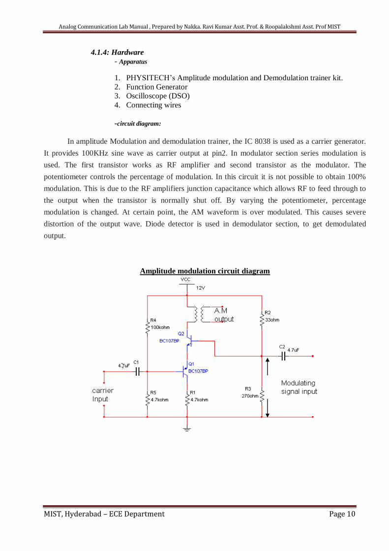
In amplitude Modulation and demodulation trainer, the IC 8038 is used as a carrier generator.
It provides 100KHz sine wave as carrier output at pin2. In modulator section series modulation is
used. The first transistor works as RF amplifier and second transistor as the modulator. The
potentiometer controls the percentage of modulation. In this circuit it is not possible to obtain 100%
modulation. This is due to the RF amplifiers junction capacitance which allows RF to feed through to
the output when the transistor is normally shut off. By varying the potentiometer, percentage
modulation is changed. At certain point, the AM waveform is over modulated. This causes severe
distortion of the output wave. Diode detector is used in demodulator section, to get demodulated
output.
Amplitude modulation circuit diagram
Analog Communication Lab Manual , Prepared by Nakka. Ravi Kumar Asst. Prof. & Roopalakshmi Asst. Prof MIST
MIST, Hyderabad – ECE Department Page 11
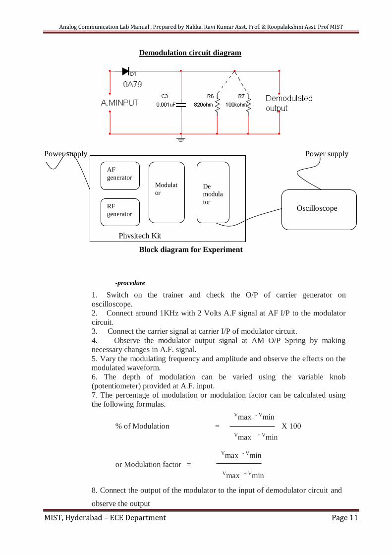
Demodulation circuit diagram
Power supply Power supply
Block diagram for Experiment
-procedure
1. Switch on the trainer and check the O/P of carrier generator on
oscilloscope.
2. Connect around 1KHz with 2 Volts A.F signal at AF I/P to the modulator
circuit.
3. Connect the carrier signal at carrier I/P of modulator circuit.
4. Observe the modulator output signal at AM O/P Spring by making
necessary changes in A.F. signal.
5. Vary the modulating frequency and amplitude and observe the effects on the
modulated waveform.
6. The depth of modulation can be varied using the variable knob
(potentiometer) provided at A.F. input.
7. The percentage of modulation or modulation factor can be calculated using
the following formulas.
Vmax - Vmin
% of Modulation = X 100
Vmax + Vmin
Vmax - Vmin
or Modulation factor =
Vmax + Vmin
8. Connect the output of the modulator to the input of demodulator circuit and
observe the output
Physitech Kit
AF
generator
Oscilloscope RF
generator
Modulat
or
De
modula
tor
Analog Communication Lab Manual , Prepared by Nakka. Ravi Kumar Asst. Prof. & Roopalakshmi Asst. Prof MIST
MIST, Hyderabad – ECE Department Page 12
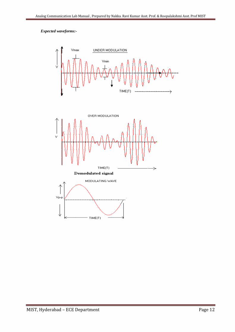
Expected waveforms:-
Analog Communication Lab Manual , Prepared by Nakka. Ravi Kumar Asst. Prof. & Roopalakshmi Asst. Prof MIST
MIST, Hyderabad – ECE Department Page 13
EXPERIMENT -2
4.2 DSB-SC modulation and demodulation
4.2.1 AIM: To study Balanced modulator for DSB-SC modulation, demodulation.
4.2.2Theory:
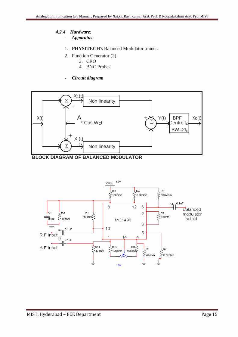
In Balanced modulator, two non-linear devices are connected in the balanced mode, so
as to suppress the carrier wave.
The Balanced Modulator consists of summing devices (operational amplifiers) and two
matched nonlinear elements. If x(t) is band limited to fx and if fc>2fx, then the band pass filter
output will be the desired product signal.
Figure shows IC that has been specifically designed for use as balanced modulators.
Figure is the 1496 balanced modulator which is manufactured by Motorola, National, and
Signetics. This device uses a differential amplifier configuration. Its carrier suppression is
rated at a minimum of -50dB with a typical value -65dB at 500 KHz.
PHYSITECH'S trainer contains a balanced modulator using a 1496 integrated circuit.
You will verify that it does suppress the carrier and also adjust it for optimum carrier
suppression.
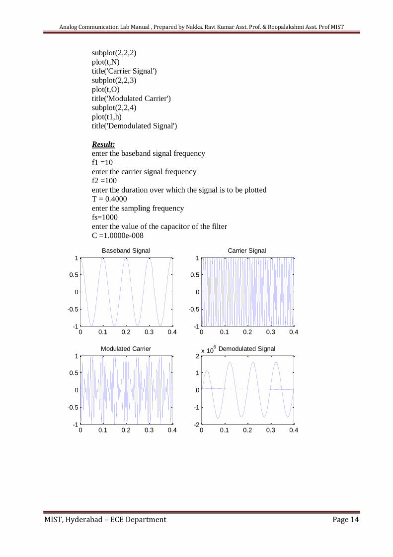
4.2.3 MATLAB program
Program:
f1=input('enter the baseband signal frequency')
f2=input('enter the carrier signal frequency')
T=input('enter the duration over which the signal is to be plotted')
fs=input('enter the sampling frequency')
t=0:T/fs:T;
M=cos(2*pi*f1*t);
N=cos(2*pi*f2*t);
O=M.*N;
P=O.*N;
C=input('enter the value of the capacitor of the filter')
R=1/(2*pi*f1*C);
H=(1/(R*C))*exp(-t/(R*C));
h=conv(H,conv(P,H));
t1=t;
for i=length(t)+1:length(h)
t1(i)=0;
end
subplot(2,2,1)
plot(t,M)
title('Baseband Signal')
Analog Communication Lab Manual , Prepared by Nakka. Ravi Kumar Asst. Prof. & Roopalakshmi Asst. Prof MIST
MIST, Hyderabad – ECE Department Page 14
subplot(2,2,2)
plot(t,N)
title('Carrier Signal')
subplot(2,2,3)
plot(t,O)
title('Modulated Carrier')
subplot(2,2,4)
plot(t1,h)
title('Demodulated Signal')
Result:
enter the baseband signal frequency
f1 =10
enter the carrier signal frequency
f2 =100
enter the duration over which the signal is to be plotted
T = 0.4000
enter the sampling frequency
fs=1000
enter the value of the capacitor of the filter
C =1.0000e-008
0 0.1 0.2 0.3 0.4-1
-0.5
0
0.5
1Baseband Signal
0 0.1 0.2 0.3 0.4-1
-0.5
0
0.5
1Carrier Signal
0 0.1 0.2 0.3 0.4-1
-0.5
0
0.5
1Modulated Carrier
0 0.1 0.2 0.3 0.4-2
-1
0
1
2x 10
6 Demodulated Signal
Analog Communication Lab Manual , Prepared by Nakka. Ravi Kumar Asst. Prof. & Roopalakshmi Asst. Prof MIST
MIST, Hyderabad – ECE Department Page 15
4.2.4 Hardware:
- Apparatus
1. PHYSITECH's Balanced Modulator trainer.
2. Function Generator (2)
3. CRO
4. BNC Probes
- Circuit diagram
+ ∑ X1(t)
Non linearity
+
X(t) AC
+ ∑
Y(t) BPF XC(t)
Cos WCt Centre fC
- BW=2fx
- +
X (t)
∑
2 Non linearity
BLOCK DIAGRAM OF BALANCED MODULATOR
Analog Communication Lab Manual , Prepared by Nakka. Ravi Kumar Asst. Prof. & Roopalakshmi Asst. Prof MIST
MIST, Hyderabad – ECE Department Page 16
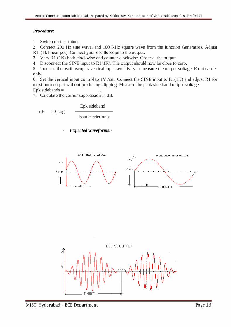
Procedure:
1. Switch on the trainer.
2. Connect 200 Hz sine wave, and 100 KHz square wave from the function Generators. Adjust
R1, (1k linear pot). Connect your oscilloscope to the output.
3. Vary R1 (1K) both clockwise and counter clockwise. Observe the output.
4. Disconnect the SINE input to R1(1K). The output should now be close to zero.
5. Increase the oscilloscope's vertical input sensitivity to measure the output voltage. E out carrier
only.
6. Set the vertical input control to 1V /cm. Connect the SINE input to R1(1K) and adjust R1 for
maximum output without producing clipping. Measure the peak side band output voltage.
Epk sidebands =_______________ .
7. Calculate the carrier suppression in dB.
Epk sideband
dB = -20 Log
Eout carrier only
- Expected waveforms:-
Analog Communication Lab Manual , Prepared by Nakka. Ravi Kumar Asst. Prof. & Roopalakshmi Asst. Prof MIST
MIST, Hyderabad – ECE Department Page 17
EXPERIMENT - 3
4.3 SSB-SC modulation and demodulation (Phase shift method)
4.3.1 Aim: To generate SSB using phase method and demodulation of SSB signal using
Synchronous detector.
4.3.2 Theory
The phase shift method makes use of two balanced modulators and two phase shift networks
as shown in fig. One of the modulators receives the carrier signal shifted by 900 and the
modulating signal with 00 (sine)phase shift, whereas the other receives modulating signal
shifted by 900 (co-sine) and the carrier (RF) signal with 00 phase shift voltage.
Both modulators produce an output consisting only of sidebands. It will be shown that both
upper sidebands lead the input carrier voltage by 900. One of the lower sidebands leads the
reference voltage by 900, and the other lags it by 900. The two lower sidebands are thus out of
phase, and when combined in the adder, they cancel each other. The upper sidebands are in
phase at the adder and therefore they add together and gives SSB upper side band signal.
When they combined in the subtractor, the upper side bands are cancel because in phase and
lower side bands add together and gives SSB lower side band signal
4.3.3 MATLAB Program Program:
f1=input('enter the base band signal frequency')
f2=input('enter the carrier signal frequency')
t=0:0.001:0.4;
fs=input('enter sampling frequency')
M=cos(2*pi*f1*t);
N=cos(2*pi*f2*t);
DSB1=M.*N;
M1=cos(2*pi*f1*t-(pi/2));
N1=cos(2*pi*f2*t-(pi/2));
DSB2=M1.*N1;
USB=DSB1-DSB2;
LSB=DSB1+DSB2;
subplot(5,1,1)
plot(t,M,'k',t,M1,'--b')
title('Base band signal and its Hilbert Transform')
subplot(5,1,2)
plot(t,N,'k',t,N1,'--b')
title('Carrier Signal and its Hilbert Transform')
subplot(5,1,3)
plot(t,USB)
title('Upper side band signal')
Analog Communication Lab Manual , Prepared by Nakka. Ravi Kumar Asst. Prof. & Roopalakshmi Asst. Prof MIST
MIST, Hyderabad – ECE Department Page 18
subplot(5,1,4)
plot(t,LSB)
title('Lower Side band Signal')
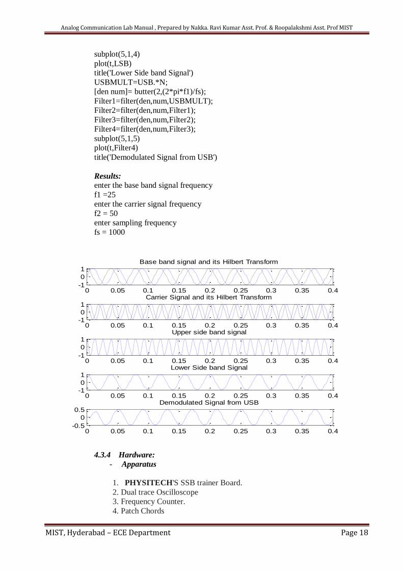
USBMULT=USB.*N;
[den num]= butter(2,(2*pi*f1)/fs);
Filter1=filter(den,num,USBMULT);
Filter2=filter(den,num,Filter1);
Filter3=filter(den,num,Filter2);
Filter4=filter(den,num,Filter3);
subplot(5,1,5)
plot(t,Filter4)
title('Demodulated Signal from USB')
Results:
enter the base band signal frequency
f1 =25
enter the carrier signal frequency
f2 = 50
enter sampling frequency
fs = 1000
4.3.4 Hardware:
- Apparatus
1. PHYSITECH'S SSB trainer Board.
2. Dual trace Oscilloscope
3. Frequency Counter.
4. Patch Chords
0 0.05 0.1 0.15 0.2 0.25 0.3 0.35 0.4-1
0
1Base band signal and its Hilbert Transform
0 0.05 0.1 0.15 0.2 0.25 0.3 0.35 0.4-1
0
1Carrier Signal and its Hilbert Transform
0 0.05 0.1 0.15 0.2 0.25 0.3 0.35 0.4-1
0
1Upper side band signal
0 0.05 0.1 0.15 0.2 0.25 0.3 0.35 0.4-1
0
1Lower Side band Signal
0 0.05 0.1 0.15 0.2 0.25 0.3 0.35 0.4-0.5
0
0.5Demodulated Signal from USB
Analog Communication Lab Manual , Prepared by Nakka. Ravi Kumar Asst. Prof. & Roopalakshmi Asst. Prof MIST
MIST, Hyderabad – ECE Department Page 19
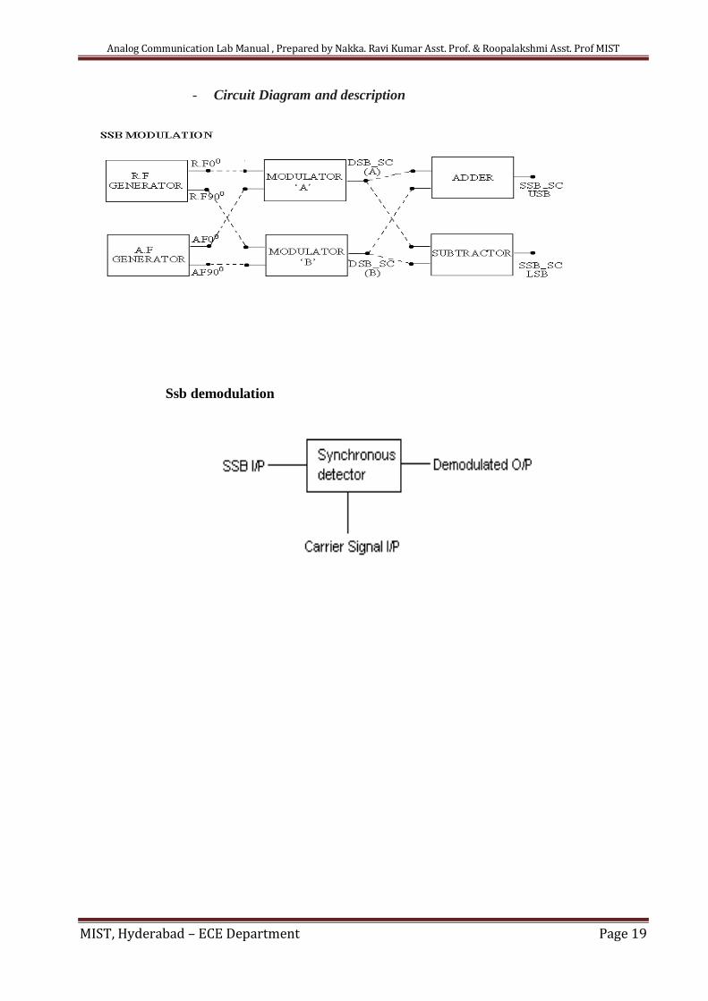
- Circuit Diagram and description
Ssb demodulation
Analog Communication Lab Manual , Prepared by Nakka. Ravi Kumar Asst. Prof. & Roopalakshmi Asst. Prof MIST
MIST, Hyderabad – ECE Department Page 20
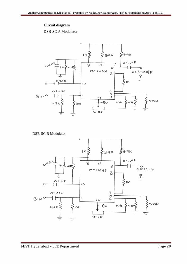
Circuit diagram
DSB-SC A Modulator
DSB-SC B Modulator
Analog Communication Lab Manual , Prepared by Nakka. Ravi Kumar Asst. Prof. & Roopalakshmi Asst. Prof MIST
MIST, Hyderabad – ECE Department Page 21
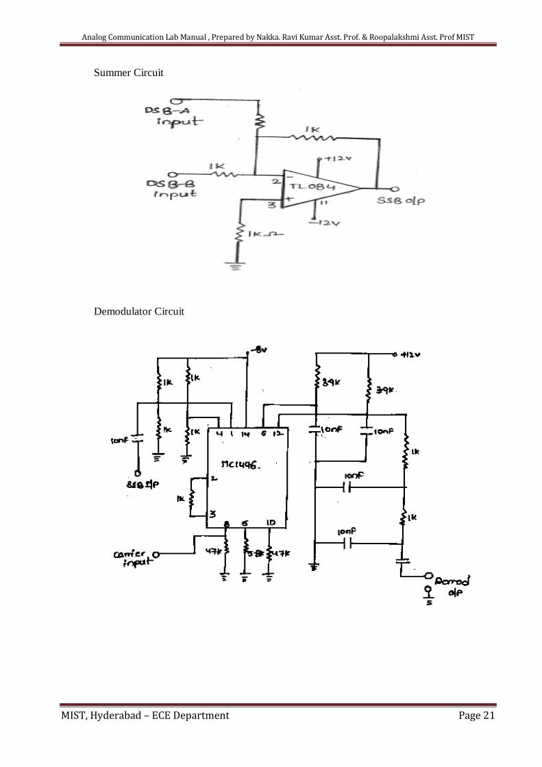
Summer Circuit
Demodulator Circuit
Analog Communication Lab Manual , Prepared by Nakka. Ravi Kumar Asst. Prof. & Roopalakshmi Asst. Prof MIST
MIST, Hyderabad – ECE Department Page 22
Circuit description: Rf generator:
Colpitts oscillator using FET is used here to generate RF signal of approximately 100KHz
frequency to use as carrier signal in this experiment. Phase shift networks are included in the same
block to produce another carrier signal of same frequency with 900 out of phase. As individual
controls are provided to vary the output voltage. Facility is provided to adjust phase of the output
signal.
Af generator:
This is a sine co-sine generator using OP-AMP. IC TL 084 is used as an active component. TL
084 is a FET input general purpose quad OP-AMP integrated circuit. A three position switch is
provided to select output frequency. An individual controls are provided to vary the output voltage.
AGC control is provided to adjust the signal shape
Balanced modulator:
This has been developed using MC 1496 IC. MC 1496 is a monolithic integrated circuit
Balanced modulator/Demodulator, is versatile and can be used up to 200MHz. These modulators are
used in this experiment to produce DSB-SC signals. Control is provided to balance the output.
Synchronous detector:
The base band signal m(t) can be uniquely recovered from a DSB-SC signal s(t) by first
multiplying s(t) with a locally generated sine wave carrier and then low pass filtering the product. It is
assumed that the local oscillator signal is exactly coherent or synchronous, in both frquency and phase
with the carrier wave c(t) used in the balanced modulator to generate s(t). This method of
demodulation is known as coherent detection or synchronous detection.
In this unit IC MC 1496 is used as synchronous demodulator. The MC 1496 is a monolithic
balanced modulator/balanced demodulator, is versatile and can be used up to 200MHz. On board
generated carrier (which is used in the modulator) is used as synchronous signal.
Summer and subtractor: These Circuits are simple summing and subtracting amplifiers using OP-AMP
. IC TL 084 is used as an active component, TL 084 is a FET input general purpose quad OP-AMP
integrated circuit.
Procedure:
1. Study the circuit operation of SSB system thoroughly. 2. Observe the output of the RF generator using CRO. There are two outputs from
the RF generator, one is direct output and the another is 900 phase shift with the direct output. The
output frequency is 100KHz and the amplitude is > 0.2 Vpp (potentiometers are provided to vary the
output amplitude).
3. Observe the output of the AF generator using CRO. There are two outputs from the AF generator, one
is direct output and the another is 900 phase shift with the direct output. AGC potentiometer is
Analog Communication Lab Manual , Prepared by Nakka. Ravi Kumar Asst. Prof. & Roopalakshmi Asst. Prof MIST
MIST, Hyderabad – ECE Department Page 23
provided to adjust the gain of the oscillator (or to set the output to good shape). And the amplitude
is 10 Vpp (potentiometers are provided to vary the output amplitude).
4. Measure and record the RF signal frequency using frequency counter.
5. Set the amplitudes of the RF signals to 0.1 Vpp and connect 00 phase shift signal to one balanced
modulator and 900 phase shift to another balanced modulator as shown in figure.
6. Select the required frequency of the AF generator with the help of switch and adjust the AGC
potentiometer until the output amplitude is ≅ 10 Vpp (when amplitude controls are in maximum
condition).
7. Measure and record the AF signals frequency using frequency counter.
8. Set the AF signal amplitudes to 8 Vpp using amplitude control and
connect to the balanced modulators as shown in below figure.
9. Observe the outputs of both the balanced modulators simultaneously using Dual trace Oscilloscope,
and adjust the balance control until you get the output wave forms (DSB-SC) as shown in figure.
10. To get SSB lower side band signal, connect balanced modulator outputs (DSB-SC signals) to
subtractor.
11. Measure and record the SSB signal frequency using counter.
12. Calculate theoretical frequency of SSB (LSB) and compare it with the practical value.
LSB=RF frequency - AF frequency
Ex : If RF frequency is 100KHz and AF frequency is 2KHz The LSB=100KHz-
2KHz=98 KHz
13. To get SSB upper side band signal, connect the output of the balanced modulator to the
summer circuit.
14. Measure and record the SSB upper side band signal frequency using counter.
15. Calculate theoretical value of the SSB(USB) frequency and compare
it with practical value.
USB=RF frequency + AF frequency
Ex : If RF frequency is 100KHz and AF frequency is 2KHz Then
USB=100KHz+2Khz =102KHz.
Demodulation of ssb signal: 16.Connect SSB signal from the summer (or) subtractor to the SSB signal input of the synchronous
detector and RF signal (00) to the RF input of the synchronous detector.
17. Observe the detector output using CRO and compare it with the modulating signal (AF signal).
18. Observe the SSB signal for the different frequencies of the modulating (AF) signal.
Analog Communication Lab Manual , Prepared by Nakka. Ravi Kumar Asst. Prof. & Roopalakshmi Asst. Prof MIST
MIST, Hyderabad – ECE Department Page 24
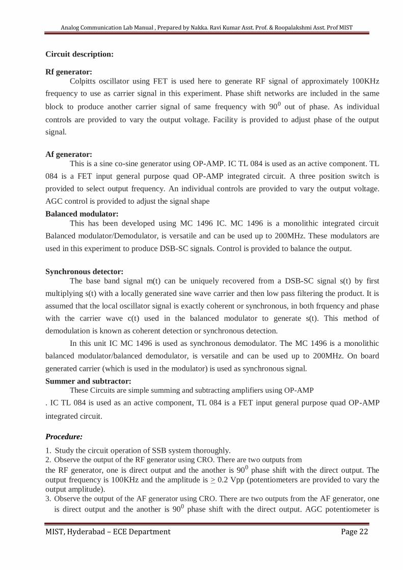
Expected waveforms
Analog Communication Lab Manual , Prepared by Nakka. Ravi Kumar Asst. Prof. & Roopalakshmi Asst. Prof MIST
MIST, Hyderabad – ECE Department Page 25
EXPERIMENT – 4
4.4 Frequency modulation and demodulation.
4.4.1 Aim: To study the functioning of frequency modulation & demodulation and to
calculate the modulation index.
4.4.2 Theory :
FM is a system in which the amplitude of the modulated carrier is kept constant, while
its frequency and rate of change are varied by the modulating signal.
By the definition of FM, the amount by which the carrier frequency is varied from
its unmodulated value, called the deviation, is made proportional to the instantaneous
amplitude of the modulating voltage. The rate at which this frequency variation changes or
takes place is equal to the modulating frequency.
FM is that form of angle modulation in which the instantaneous frequency fi(t) is
varied linearly with the message signal m(t), as
fi(t) =fC+kf m(t)
The term fc represents the frequency of the unmodulated carrier, and the constant Kf
represents the frequency sensitivity of the modulator expressed in Hertz per volt.
Unlike AM, the spectrum of an FM signal is not related in a simple manner to that of
modulating signal, rather its analysis is much more difficult than that of an AM signal.
Generation of FM signals: There are essentially two basic methods of generating frequency modulated signals,
namely, direct FM and indirect FM. In the direct method, the carrier frequency is directly
varied in accordance with the input base band signal, which is readily accomplished using a
voltage-controlled oscillator. In the indirect method, the modulating signal is first used to
produce a narrow band FM signal, and frequency multiplication is next used to increase the
frequency deviation to the desired level. The indirect method is the preferred choice for FM
when the stability of carrier frequency is of major concern as in commercial radio broad
casting.
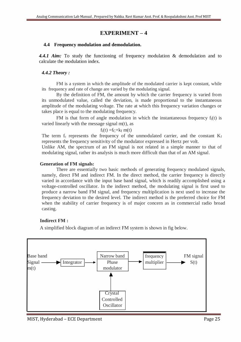
Indirect FM : A simplified block diagram of an indirect FM system is shown in fig below.
Base band
Narrow band
FM signal
frequency
Signal
Integrator
Phase
multiplier
S(t)
m(t)
modulator
Crystal Controlled Oscillator
Analog Communication Lab Manual , Prepared by Nakka. Ravi Kumar Asst. Prof. & Roopalakshmi Asst. Prof MIST
MIST, Hyderabad – ECE Department Page 26
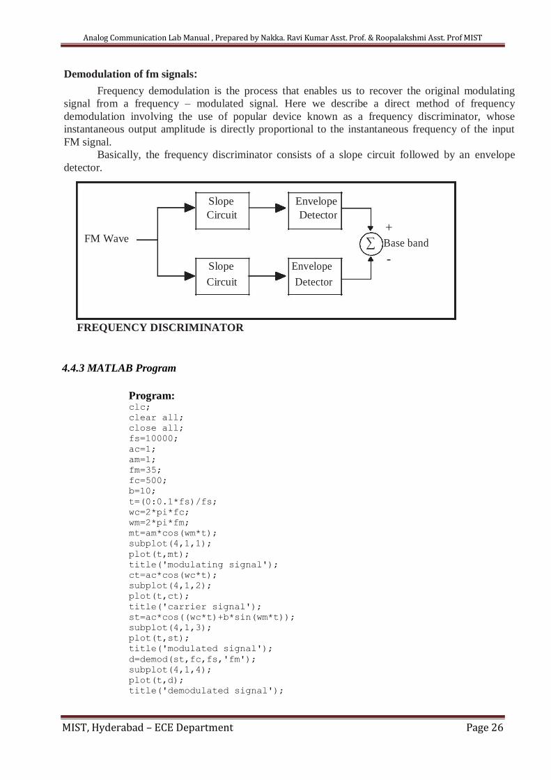
Demodulation of fm signals:
Frequency demodulation is the process that enables us to recover the original modulating
signal from a frequency – modulated signal. Here we describe a direct method of frequency
demodulation involving the use of popular device known as a frequency discriminator, whose
instantaneous output amplitude is directly proportional to the instantaneous frequency of the input
FM signal.
Basically, the frequency discriminator consists of a slope circuit followed by an envelope
detector.
Slope Envelope
Circuit Detector
FM Wave +
∑ Base band
Slope Envelope -
Circuit Detector
FREQUENCY DISCRIMINATOR
4.4.3 MATLAB Program
Program: clc; clear all; close all; fs=10000; ac=1; am=1; fm=35; fc=500; b=10; t=(0:0.1*fs)/fs; wc=2*pi*fc; wm=2*pi*fm; mt=am*cos(wm*t); subplot(4,1,1); plot(t,mt); title('modulating signal'); ct=ac*cos(wc*t); subplot(4,1,2); plot(t,ct); title('carrier signal'); st=ac*cos((wc*t)+b*sin(wm*t)); subplot(4,1,3); plot(t,st); title('modulated signal'); d=demod(st,fc,fs,'fm'); subplot(4,1,4); plot(t,d); title('demodulated signal');
Analog Communication Lab Manual , Prepared by Nakka. Ravi Kumar Asst. Prof. & Roopalakshmi Asst. Prof MIST
MIST, Hyderabad – ECE Department Page 27
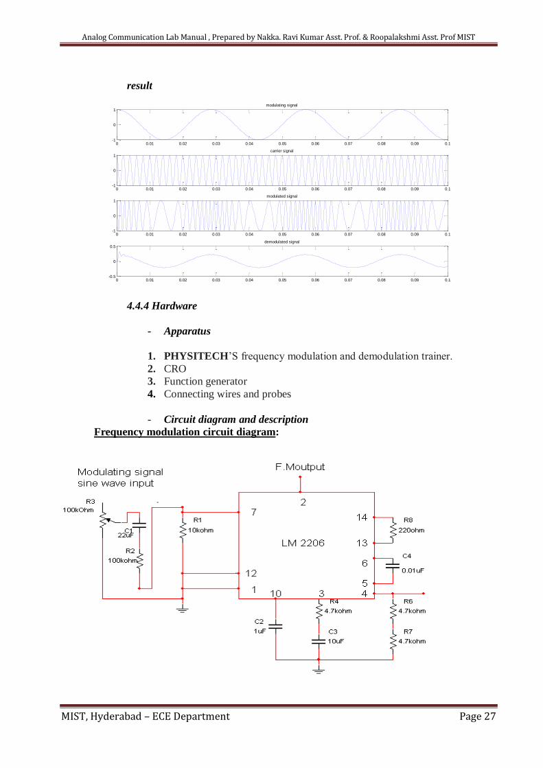
result
4.4.4 Hardware
- Apparatus
1. PHYSITECH’S frequency modulation and demodulation trainer.
2. CRO
3. Function generator
4. Connecting wires and probes
- Circuit diagram and description
Frequency modulation circuit diagram:
0 0.01 0.02 0.03 0.04 0.05 0.06 0.07 0.08 0.09 0.1-1
0
1modulating signal
0 0.01 0.02 0.03 0.04 0.05 0.06 0.07 0.08 0.09 0.1-1
0
1carrier signal
0 0.01 0.02 0.03 0.04 0.05 0.06 0.07 0.08 0.09 0.1-1
0
1modulated signal
0 0.01 0.02 0.03 0.04 0.05 0.06 0.07 0.08 0.09 0.1-0.5
0
0.5demodulated signal
Analog Communication Lab Manual , Prepared by Nakka. Ravi Kumar Asst. Prof. & Roopalakshmi Asst. Prof MIST
MIST, Hyderabad – ECE Department Page 28
Frequency demodulation circuit diagram:
Procedure:
1. Switch on the PHYSITECH’S experimental board.
2. Connect Oscilloscope to the FM O/P and observe that carrier frequency at
that point without any A.F. input.
3. Connect around 7KHz sine wave (A.F. signal) to the input of the frequency
modulator (At AF input).
4. Now observe the frequency modulation output on the 1st channel of on CRO and
adjust the amplitude of the AF signal to get clear frequency modulated wave form.
5. Vary the modulating frequency (A.F.Signal), and amplitude and observe the effects
on the modulated waveform.
6. Connect the FM o/p to the FM i/p of De-modulator.
7. Vary the potentiometer provided in the demodulator section.
8. Observe the output at demodulation o/p on second channel of CRO
Analog Communication Lab Manual , Prepared by Nakka. Ravi Kumar Asst. Prof. & Roopalakshmi Asst. Prof MIST
MIST, Hyderabad – ECE Department Page 29
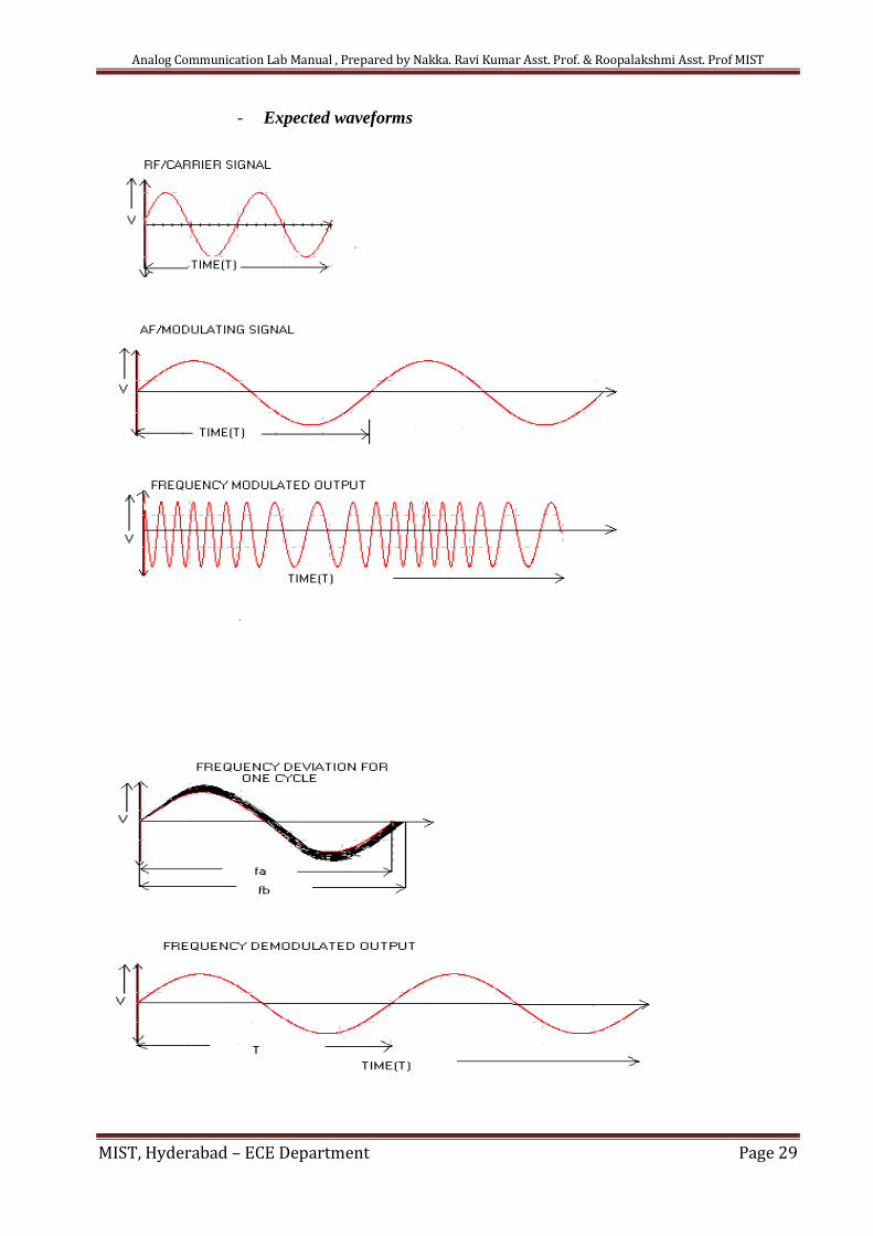
- Expected waveforms
Analog Communication Lab Manual , Prepared by Nakka. Ravi Kumar Asst. Prof. & Roopalakshmi Asst. Prof MIST
MIST, Hyderabad – ECE Department Page 30
EXPERIMENT - 5
4.5 Study of Spectrum Analyzer
4.5.1 Aim: To study the Spectrum analyzer
4.5.2 Theory
To study the frequency response of the signals, we use spectrum analyzers. In
theory, applying Fourier transform on time domain signals gives their frequency
domain response. In hardware, the frequency response of the time domain signals is
obtained by spectrum analyzer.
4.5.3 MATLAB Program
Program: %program of spectrum analyzer and analysis of am and fm signals close all clear all clc Fs = 100; %sampling frq t = [0:2*Fs+1]'/Fs; Fc = 10; % Carrier frequency x = sin(2*pi*2*t); % message signal Ac=1; %compute spectra of am
xam=ammod(x,Fc,Fs,0,Ac); zam = fft(xam); zam = abs(zam(1:length(zam)/2+1)); frqam = [0:length(zam)-1]*Fs/length(zam)/2; % compute spectra of dsbsc ydouble = ammod(x,Fc,Fs, 3.14,0); zdouble = fft(ydouble); zdouble = abs(zdouble(1:length(zdouble)/2+1)); frqdouble = [0:length(zdouble)-1]*Fs/length(zdouble)/2; % compute spectra of ssb ysingle = ssbmod(x,Fc,Fs,0,'upper'); zsingle = fft(ysingle); zsingle = abs(zsingle(1:length(zsingle)/2+1)); frqsingle = [0:length(zsingle)-1]*Fs/length(zsingle)/2; % Plot spectrums of am dsbsc and ssb figure; subplot(3,1,1); plot(frqam,zam); title('Spectrum of am signal'); subplot(3,1,2); plot(frqdouble,zdouble); title('Spectrum of double-sideband signal'); subplot(3,1,3); plot(frqsingle,zsingle); title('Spectrum of single-sideband signal'); % spectrum of fm xfm=fmmod(x,Fc,Fs,10); zfm = fft(xfm); zfm = abs(zfm(1:length(zfm)/2+1)); frqfm = [0:length(zfm)-1]*Fs/length(zfm)/2; figure; plot(frqfm,zfm); title('Spectrum of fm signal');
Analog Communication Lab Manual , Prepared by Nakka. Ravi Kumar Asst. Prof. & Roopalakshmi Asst. Prof MIST
MIST, Hyderabad – ECE Department Page 31
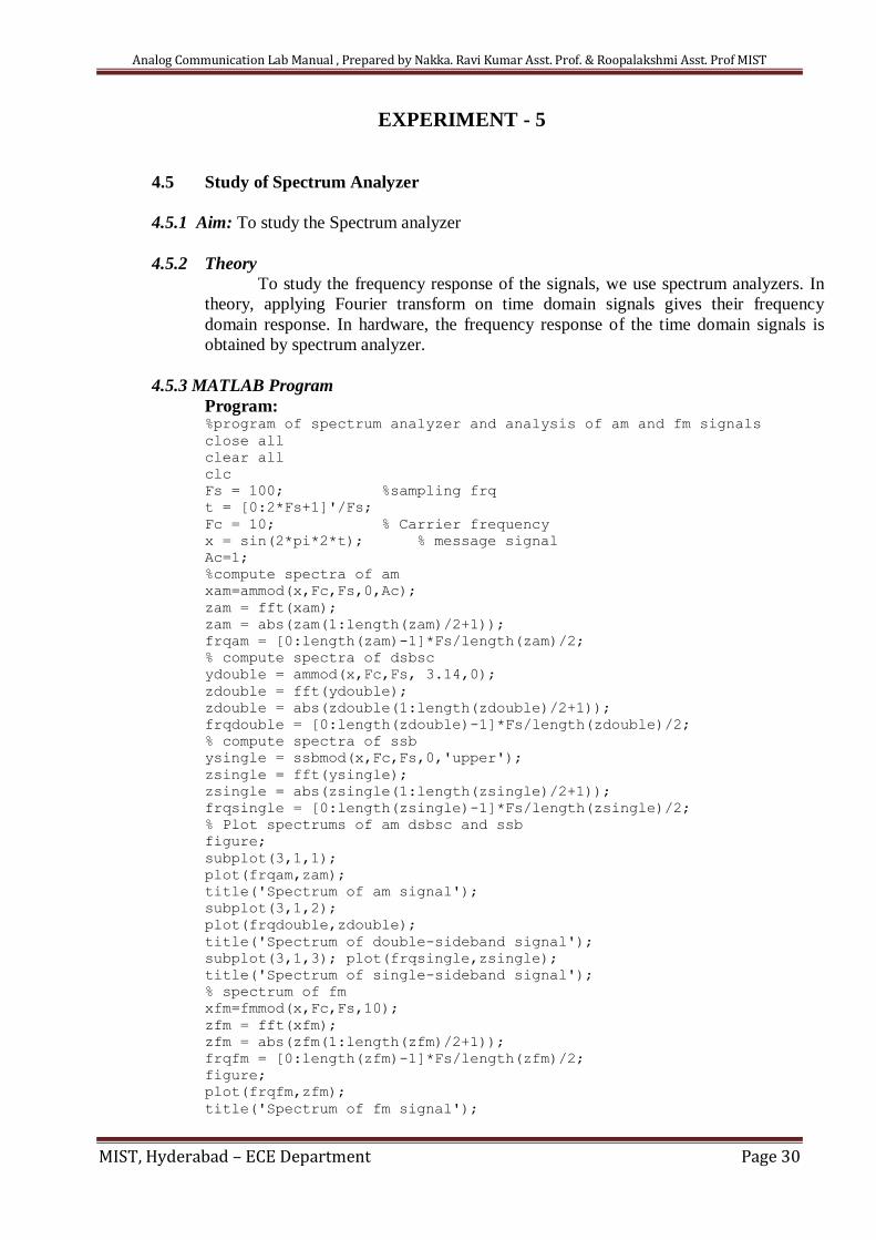
Expected waveforms:
4.5.4 Hardware
- Apparatus
1. RF generator
2. Function generator
3. Spectrum analyzer

Analog Communication Lab Manual , Prepared by Nakka. Ravi Kumar Asst. Prof. & Roopalakshmi Asst. Prof MIST
MIST, Hyderabad – ECE Department Page 32
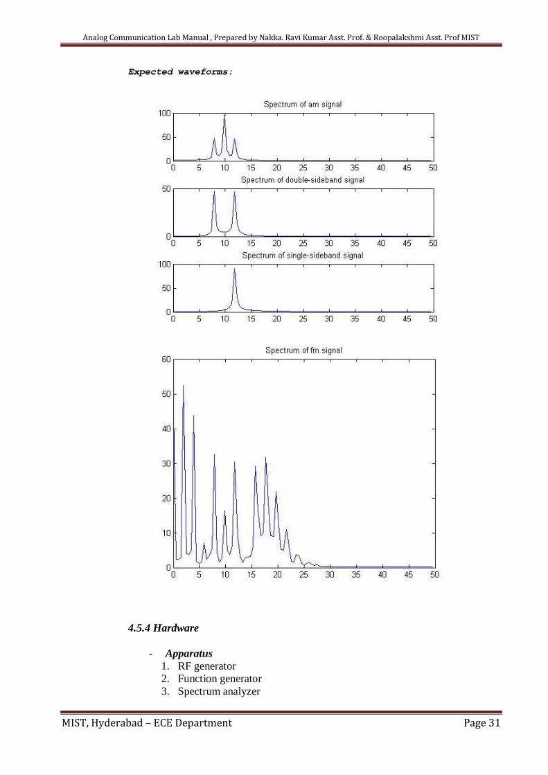
- Circuit diagram
Power supply
- Procedure:
To check the frequency spectrum RF signal, the RF generator’s output is
connected to the spectrum analyzer as shown in the picture above.
The frequency spectrums Square waves, triangular waves can also be analyzed
with the Function generator connected with the spectrum analyzer.
- Expected waveforms:
RF Spectrum
Spectrum
analyzer
RF
generator
Analog Communication Lab Manual , Prepared by Nakka. Ravi Kumar Asst. Prof. & Roopalakshmi Asst. Prof MIST
MIST, Hyderabad – ECE Department Page 33
EXPERIMENT – 6
4.6 Pre-emphasis and De-emphasis
4.6.1 AIM: To study the functioning of Pre-Emphasis and De-Emphasis circuits
4.6.2 Theory
Frequency modulation is much more immune to noise than amplitude
modulation and is significantly more immune than phase modulation. The threshold
effect is more serious in FM as compared to AM, because in FM, the signal to noise
ratio at the input of a detector, at which threshold effect starts, is higher. Lower the
threshold level, better is the system because threshold can be avoided at a
comparatively lower ratio, and a small signal is needed to avoid threshold for an
equivalent noise power. Hence, it is desirable to lower the threshold level in the FM
receivers. The process of lowering the threshold level is known as threshold
improvement, or threshold reduction. Two methods are used for the improvement of
the threshold. Pre-Emphasis and De-Emphasis circuits.
FMFB (Frequency Modulation with Feed Back.)
PRE-EMPHASIS AND DE-EMPHASIS:
The noise triangle shows, noise has a greater effect on the higher modulating
frequencies than on the lower ones. Thus, if the higher frequencies were artificially
boosted at the transmitter and correspondingly cut at the receiver, an improvement in
noise immunity could be expected, thereby increasing the signal-to-noise ratio. This
boosting of the higher modulating frequencies, in accordance with a prearranged curve,
is termed pre-emphasis, and the compensation at the receiver is called de-emphasis.
4.6.3 MATLAB program and description
% program for Pre-Emphasis and De-Emphasis
close all
clear all
clc
num_samples = 2^13;
fs=5000;
Ts=1/fs;
fm1=20;
fm2=30;
fc=200;
t=(0:num_samples-1)*Ts;
f=(-num_samples/2:num_samples/2-1)*fs/num_samples;
mt=sin(2*pi*fm1*t);
Mf=fftshift(abs(fft(mt)));
f_cutoff_pe=15;
Wn_pe=f_cutoff_pe/(fs/2);
[b_pe,a_pe]=butter(1,Wn_pe);
[H_pe,W]=freqz(a_pe,b_pe);
a_de=b_pe;
b_de=a_pe;
[H_de,W]=freqz(a_de,b_de);
mt_pe=filter(a_pe,b_pe,mt);
Analog Communication Lab Manual , Prepared by Nakka. Ravi Kumar Asst. Prof. & Roopalakshmi Asst. Prof MIST
MIST, Hyderabad – ECE Department Page 34
Mf_pe=fftshift(abs(fft(mt_pe)));
figure(1)
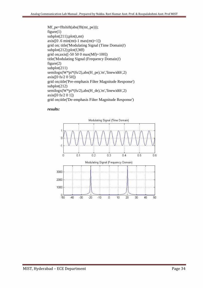
subplot(211);plot(t,mt)
axis([0 .6 min(mt)-1 max(mt)+1])
grid on; title('Modulating Signal (Time Domain)')
subplot(212);plot(f,Mf)
grid on;axis([-50 50 0 max(Mf)+100])
title('Modulating Signal (Frequency Domain)')
figure(2)
subplot(211)
semilogx(W*pi*(fs/2),abs(H_pe),'m','linewidth',2)
axis([0 fs/2 0 50])
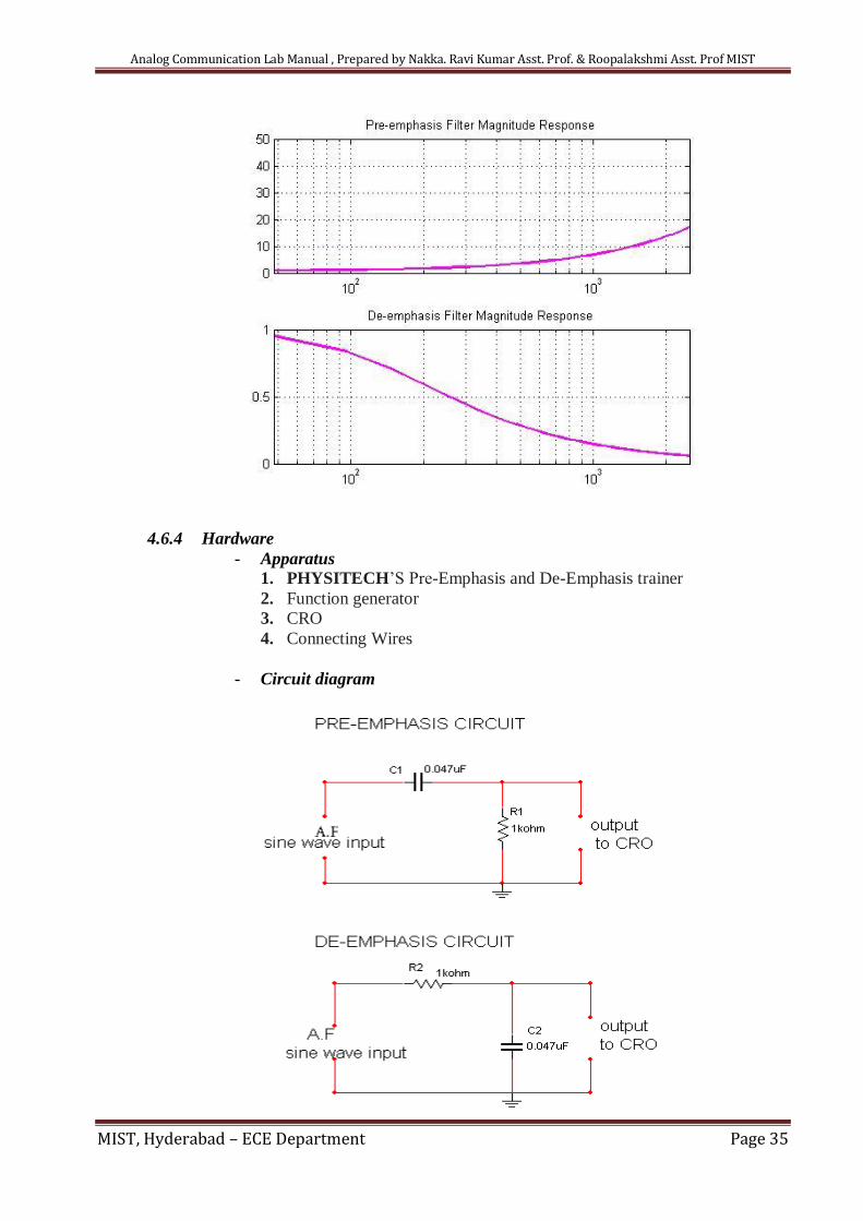
grid on;title('Pre-emphasis Filter Magnitude Response')
subplot(212)
semilogx(W*pi*(fs/2),abs(H_de),'m','linewidth',2)
axis([0 fs/2 0 1])
grid on;title('De-emphasis Filter Magnitude Response')
results:
Analog Communication Lab Manual , Prepared by Nakka. Ravi Kumar Asst. Prof. & Roopalakshmi Asst. Prof MIST
MIST, Hyderabad – ECE Department Page 35
4.6.4 Hardware
- Apparatus
1. PHYSITECH’S Pre-Emphasis and De-Emphasis trainer
2. Function generator
3. CRO
4. Connecting Wires
- Circuit diagram
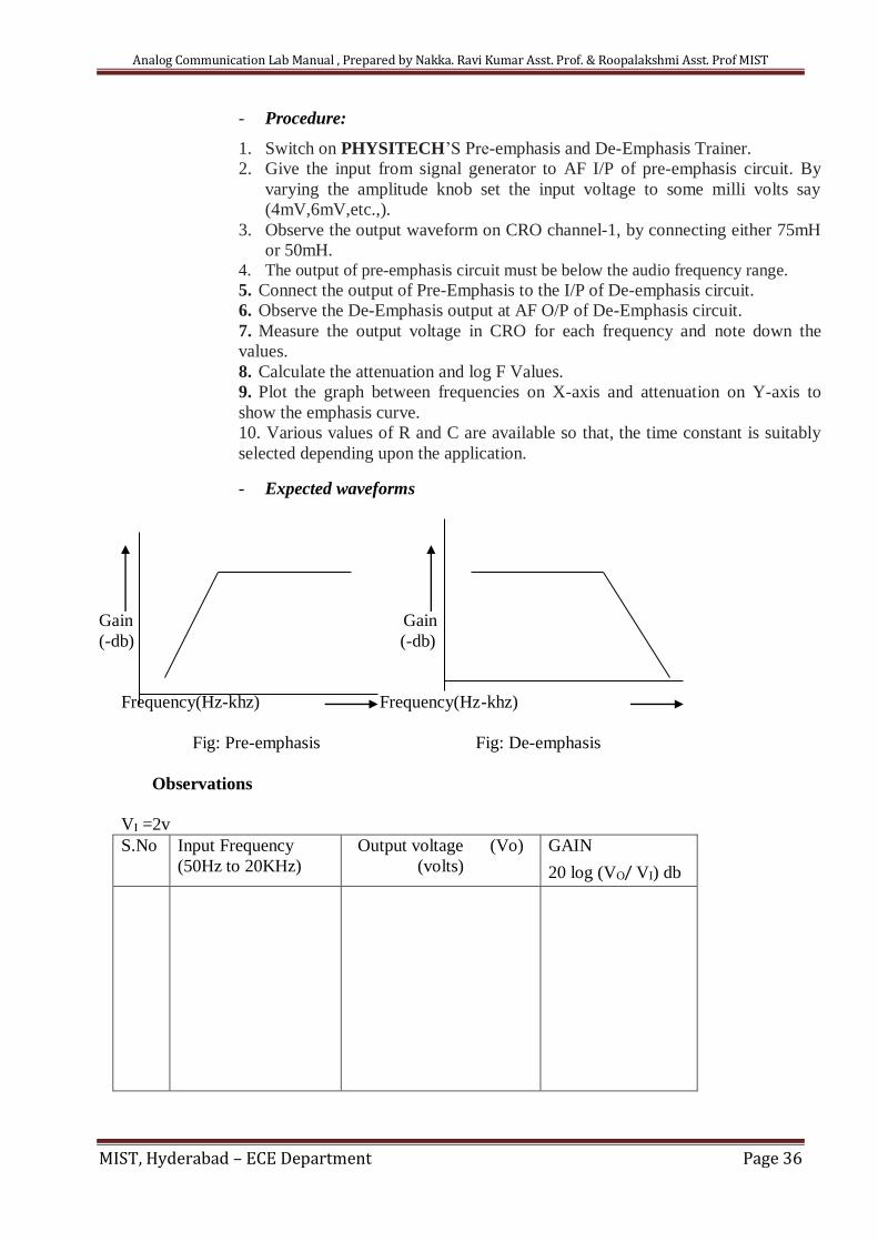
Analog Communication Lab Manual , Prepared by Nakka. Ravi Kumar Asst. Prof. & Roopalakshmi Asst. Prof MIST
MIST, Hyderabad – ECE Department Page 36
- Procedure:
1. Switch on PHYSITECH’S Pre-emphasis and De-Emphasis Trainer.
2. Give the input from signal generator to AF I/P of pre-emphasis circuit. By
varying the amplitude knob set the input voltage to some milli volts say
(4mV,6mV,etc.,).
3. Observe the output waveform on CRO channel-1, by connecting either 75mH
or 50mH. 4. The output of pre-emphasis circuit must be below the audio frequency range.
5. Connect the output of Pre-Emphasis to the I/P of De-emphasis circuit.
6. Observe the De-Emphasis output at AF O/P of De-Emphasis circuit.
7. Measure the output voltage in CRO for each frequency and note down the
values.
8. Calculate the attenuation and log F Values.
9. Plot the graph between frequencies on X-axis and attenuation on Y-axis to
show the emphasis curve.
10. Various values of R and C are available so that, the time constant is suitably
selected depending upon the application.
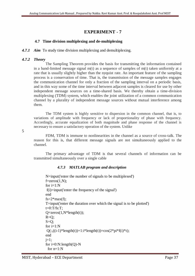
- Expected waveforms
Gain Gain
(-db) (-db)
Frequency(Hz-khz) Frequency(Hz-khz)
Fig: Pre-emphasis Fig: De-emphasis
Observations
VI =2v
S.No Input Frequency
(50Hz to 20KHz)
Output voltage (Vo)
(volts)
GAIN
20 log (VO/ VI) db
Analog Communication Lab Manual , Prepared by Nakka. Ravi Kumar Asst. Prof. & Roopalakshmi Asst. Prof MIST
MIST, Hyderabad – ECE Department Page 37
EXPERIMENT - 7
4.7 Time division multiplexing and de-multiplexing
4.7.1 Aim To study time division multiplexing and demultiplexing.
4.7.2 Theory
The Sampling Theorem provides the basis for transmitting the information contained
in a band-limited message signal m(t) as a sequence of samples of m(t) taken uniformly at a
rate that is usually slightly higher than the nyquist rate. An important feature of the sampling
process is a conservation of time. That is, the transmission of the message samples engages
the communication channel for only a fraction of the sampling interval on a periodic basis,
and in this way some of the time interval between adjacent samples is cleared for use by other
independent message sources on a time-shared basis. We thereby obtain a time-division
multiplexing (TDM) system, which enables the joint utilization of a common communication
channel by a plurality of independent message sources without mutual interference among
them.
The TDM system is highly sensitive to dispersion in the common channel, that is, to
variations of amplitude with frequency or lack of proportionality of phase with frequency.
Accordingly, accurate equalization of both magnitude and phase response of the channel is
necessary to ensure a satisfactory operation of the system. Unlike
5
FDM, TDM is immune to nonlinearities in the channel as a source of cross-talk. The
reason for this is, that different message signals are not simultaneously applied to the
channel.
The primary advantage of TDM is that several channels of information can be
transmitted simultaneously over a single cable
4.7.3 MATLAB program and description
N=input('enter the number of signals to be multiplexed')
f=zeros(1,N);
for i=1:N
f(i)=input('enter the frequency of the signal')
end
fs=2*max(f);
T=input('enter the duration over which the signal is to be plotted')
t=0:T/fs:T;
Q=zeros(1,N*length(t));
R=Q;
S=Q;
for i=1:N
Q(:,((i-1)*length(t))+1:i*length(t))=cos(2*pi*f(i)*t);
end
j=1;
for i=0:N:length(Q)-N
for n=1:N
Analog Communication Lab Manual , Prepared by Nakka. Ravi Kumar Asst. Prof. & Roopalakshmi Asst. Prof MIST
MIST, Hyderabad – ECE Department Page 38
R(i+n)=Q(j+(n-1)*length(t));
S(j+(n-1)*length(t))=R(i+n);
end
j=j+1;
end
t1=0:T/fs:N*T;
for i=length(t1)+1:length(Q)
t1(i)=t1(length(t1));
end
subplot(N+2,1,1)
plot(t1,Q)
title('Signals to be Multiplexed')
subplot(N+2,1,2)
stem(t1,R)
title('Multiplexed Signal')
for i=1:N
subplot(N+2, 1,i+2)
plot(t,S(:,((i-1)*length(t))+1:i*length(t)))
title('De-multiplexed Signal' )
end
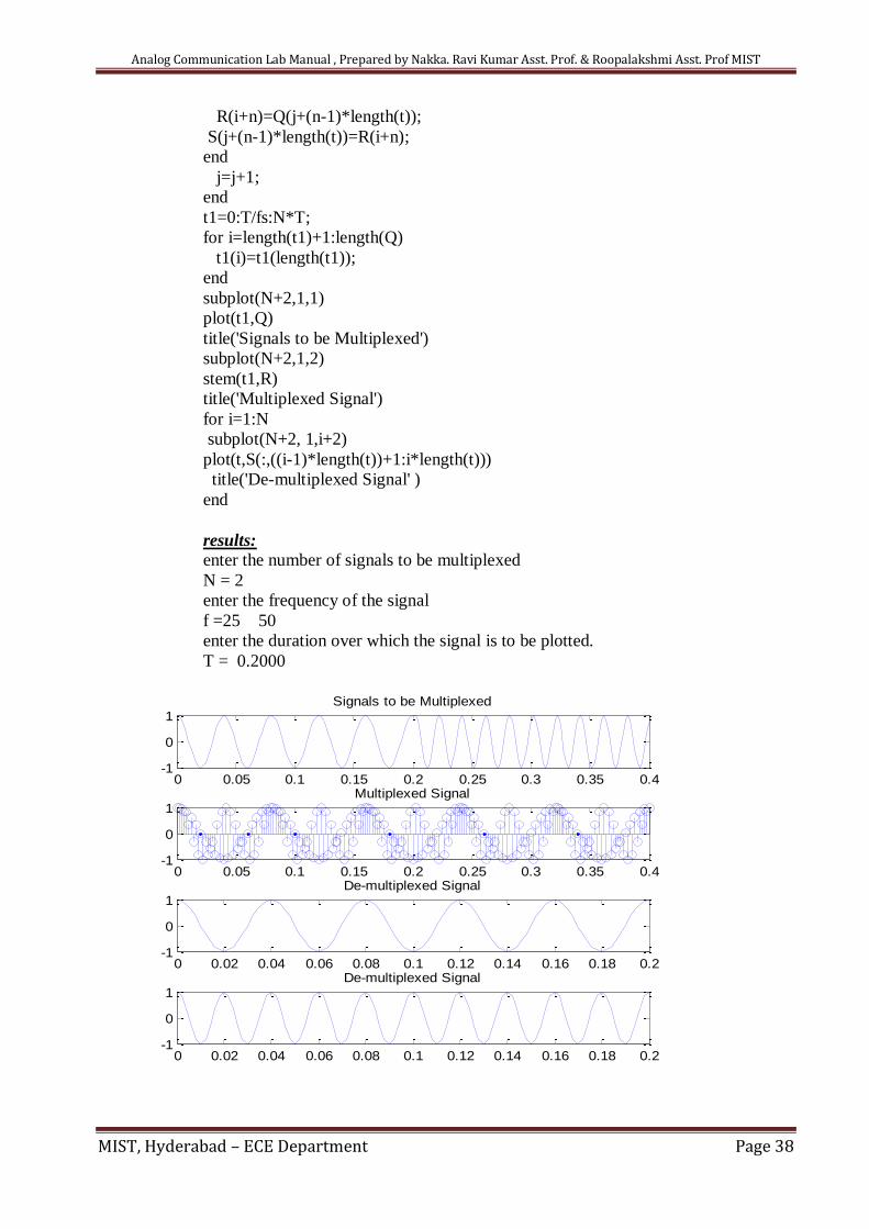
results: enter the number of signals to be multiplexed
N = 2
enter the frequency of the signal
f =25 50
enter the duration over which the signal is to be plotted.
T = 0.2000
0 0.05 0.1 0.15 0.2 0.25 0.3 0.35 0.4-1
0
1Signals to be Multiplexed
0 0.05 0.1 0.15 0.2 0.25 0.3 0.35 0.4-1
0
1Multiplexed Signal
0 0.02 0.04 0.06 0.08 0.1 0.12 0.14 0.16 0.18 0.2-1
0
1De-multiplexed Signal
0 0.02 0.04 0.06 0.08 0.1 0.12 0.14 0.16 0.18 0.2-1
0
1De-multiplexed Signal
Analog Communication Lab Manual , Prepared by Nakka. Ravi Kumar Asst. Prof. & Roopalakshmi Asst. Prof MIST
MIST, Hyderabad – ECE Department Page 39
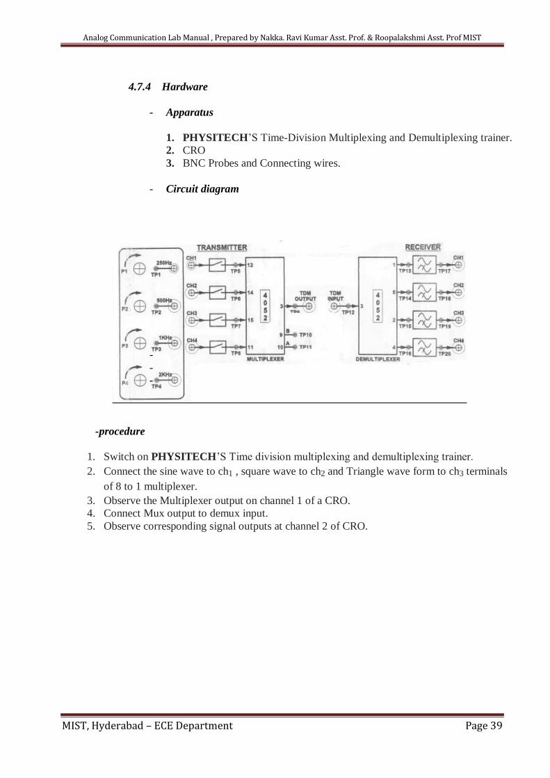
4.7.4 Hardware
- Apparatus
1. PHYSITECH’S Time-Division Multiplexing and Demultiplexing trainer.
2. CRO
3. BNC Probes and Connecting wires.
- Circuit diagram
-
-
-
-procedure
1. Switch on PHYSITECH’S Time division multiplexing and demultiplexing trainer.
2. Connect the sine wave to ch1 , square wave to ch2 and Triangle wave form to ch3 terminals
of 8 to 1 multiplexer.
3. Observe the Multiplexer output on channel 1 of a CRO.
4. Connect Mux output to demux input.
5. Observe corresponding signal outputs at channel 2 of CRO.
Analog Communication Lab Manual , Prepared by Nakka. Ravi Kumar Asst. Prof. & Roopalakshmi Asst. Prof MIST
MIST, Hyderabad – ECE Department Page 40
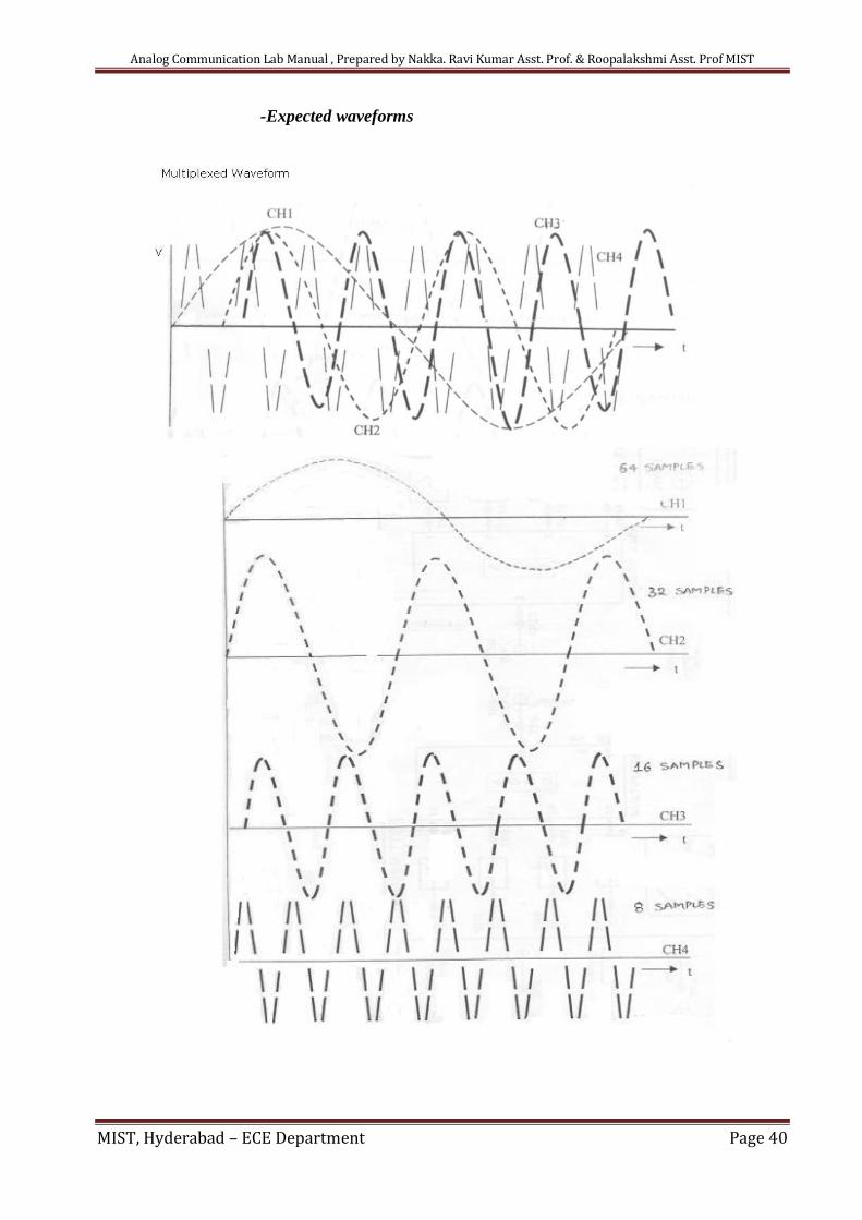
-Expected waveforms
Analog Communication Lab Manual , Prepared by Nakka. Ravi Kumar Asst. Prof. & Roopalakshmi Asst. Prof MIST
MIST, Hyderabad – ECE Department Page 41
EXPERIMENT - 8
4.8 Frequency division multiplexing and de-multiplexing
4.8.1 Aim: To study Frequency division multiplexing and de-multiplexing
4.8.2 Theory
In any communication system, there will be a transmitter, a receiver and
channel. In a multiple subscriber two way communication system, there will be
more transmitters at the transmitting end and more receivers at the receiving end. In
general channel is only one. For the maximum utilization of the channel, all the
signals which are meant to be transmitted, which are occupying the same
bandwidth, need to be multiplexed to avoid mixing with each other and to avoid
noise interruption. This multiplexing can be done either in time domain or in
frequency domain. If it is done in time domain, it is called Time Division
Multiplexing (TDM), which is described in experiment-7. On the other hand, if the
multiplexing is done in the frequency domain, as in the case with AM, DSB-SC,
SSB-SC or FM, it is called Frequency Division Multiplexing (FDM). At the
destination end, a reverse process of multiplexing need to be done. This is known as
de-multiplexing. In this experiment we will study Frequency division multiplexing
and de-multiplexing.
4.8.3 MATLAB program and description
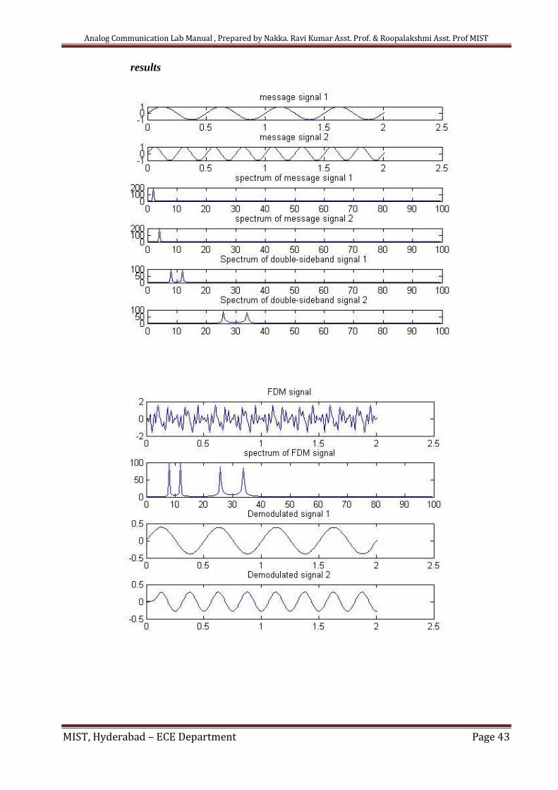
Program: %program for FDM and Demultiplexing close all clear all clc Fs = 200; %sampling frq t = [0:2*Fs+1]'/Fs; Fc1 = 10; % Carrier frequency F1 = 2; x1 = sin(2*pi*F1*t); % message signal Fc2 = 30; % Carrier frequency F2 = 4; x2 = sin(2*pi*F2*t); % message signal % compute spectra of message signal z1 = fft(x1); z1 = abs(z1(1:length(z1)/2+1)); frq1 = [0:length(z1)-1]*Fs/length(z1)/2; z2 = fft(x2); z2 = abs(z2(1:length(z2)/2+1)); frq2 = [0:length(z2)-1]*Fs/length(z2)/2; % compute spectra of dsbsc ydouble1 = ammod(x1,Fc1,Fs); zdouble1 = fft(ydouble1); zdouble1 = abs(zdouble1(1:length(zdouble1)/2+1)); frqdouble1 = [0:length(zdouble1)-1]*Fs/length(zdouble1)/2; ydouble2 = ammod(x2,Fc2,Fs); zdouble2 = fft(ydouble2); zdouble2 = abs(zdouble2(1:length(zdouble2)/2+1)); frqdouble2 = [0:length(zdouble2)-1]*Fs/length(zdouble2)/2; % Plot spectrums of message signal and dsbsc figure; subplot(6,1,1); plot(t,x1);
Analog Communication Lab Manual , Prepared by Nakka. Ravi Kumar Asst. Prof. & Roopalakshmi Asst. Prof MIST
MIST, Hyderabad – ECE Department Page 42
title('message signal 1'); subplot(6,1,2); plot(t,x2); title('message signal 2'); subplot(6,1,3); plot(frq1,z1); axis([0 100 0 200]); title('spectrum of message signal 1'); subplot(6,1,4); plot(frq2,z2); axis([0 100 0 200]); title('spectrum of message signal 2'); subplot(6,1,5); plot(frqdouble1,zdouble1); title('Spectrum of double-sideband signal 1'); subplot(6,1,6); plot(frqdouble2,zdouble2); title('Spectrum of double-sideband signal 2'); %FDM signal m=ydouble1+ydouble2; zfdm = fft(m); zfdm = abs(zfdm(1:length(zfdm)/2+1)); frqfdm = [0:length(zfdm)-1]*Fs/length(zfdm)/2; %Seperating AM-DSB-SC-1 from FDM signal [den1 num1]=butter(1,(Fc1-F1)/50,'high'); M11=filter(den1,num1,m); [den2 num2]=butter(1,(Fc1+F1)/50,'low'); M12=filter(den2,num2,M11); y1 = amdemod(M12,Fc1,Fs); %seperating AM-DSB-SC-2 from FDM signal [den3 num3]=butter(1,(Fc2-F2)/50,'high'); M21=filter(den3,num3,m); [den4 num4]=butter(1,(Fc2+F2)/50,'low'); M22=filter(den4,num4,M21); y2 = amdemod(M22,Fc2,Fs); [den5 num5]=butter(3,F2/40,'low'); ba2=filter(den5,num5,y2); ba22=filter(den5,num5,ba2); % Plot FDM and spectrum of FDM and demultiplexed and demodulated
signals figure; subplot(4,1,1); plot(t,m); title('FDM signal'); subplot(4,1,2); plot(frqfdm,zfdm); title('spectrum of FDM signal'); subplot(4,1,3); plot(t,y1) title('Demodulated signal 1') subplot(4,1,4); plot(t,ba22) title('Demodulated signal 2')
Analog Communication Lab Manual , Prepared by Nakka. Ravi Kumar Asst. Prof. & Roopalakshmi Asst. Prof MIST
MIST, Hyderabad – ECE Department Page 43
results
Analog Communication Lab Manual , Prepared by Nakka. Ravi Kumar Asst. Prof. & Roopalakshmi Asst. Prof MIST
MIST, Hyderabad – ECE Department Page 44
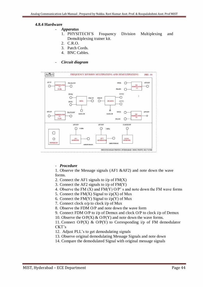
4.8.4 Hardware
- Apparatus
1. PHYSITECH’S Frequency Division Multiplexing and
Demultiplexing trainer kit.
2. C.R.O.
3. Patch Cords.
4. BNC Cables.
- Circuit diagram
- Procedure
1. Observe the Message signals (AF1 &AF2) and note down the wave
forms.
2. Connect the AF1 signals to i/p of FM(X)
3. Connect the AF2 signals to i/p of FM(Y)
4. Observe the FM (X) and FM(Y) O/P’ s and note down the FM wave forms
5. Connect the FM(X) Signal to i/p(X) of Mux
6. Connect the FM(Y) Signal to i/p(Y) of Mux
7. Connect clock o/p to clock i/p of Mux
8. Observe the FDM O/P and note down the wave form
9. Connect FDM O/P to i/p of Demux and clock O/P to clock i/p of Demux
10. Observe the O/P(X) & O/P(Y) and note down the wave forms.
11. Connect O/P(X) & O/P(Y) to Corresponding i/p of FM demodulator
CKT’s
12. Adjust PLL’s to get demodulating signals
13. Observe original demodulating Message Signals and note down
14. Compare the demodulated Signal with original message signals
Analog Communication Lab Manual , Prepared by Nakka. Ravi Kumar Asst. Prof. & Roopalakshmi Asst. Prof MIST
MIST, Hyderabad – ECE Department Page 45
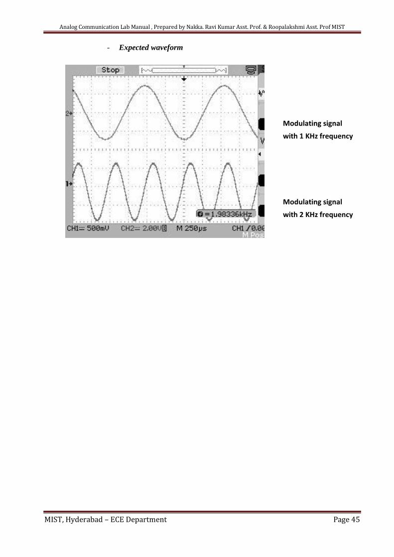
- Expected waveform
Modulating signal
with 1 KHz frequency
Modulating signal
with 2 KHz frequency
Analog Communication Lab Manual , Prepared by Nakka. Ravi Kumar Asst. Prof. & Roopalakshmi Asst. Prof MIST
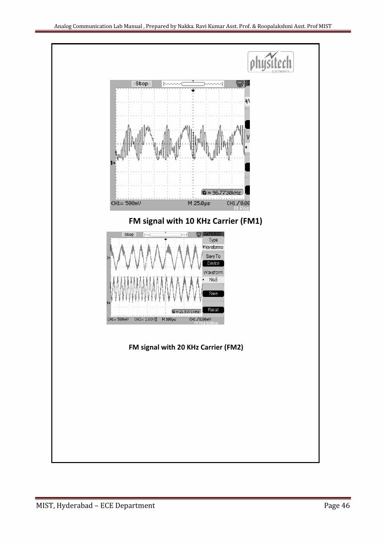
MIST, Hyderabad – ECE Department Page 46
FM signal with 10 KHz Carrier (FM1)
FM signal with 20 KHz Carrier (FM2)
Analog Communication Lab Manual , Prepared by Nakka. Ravi Kumar Asst. Prof. & Roopalakshmi Asst. Prof MIST
MIST, Hyderabad – ECE Department Page 47
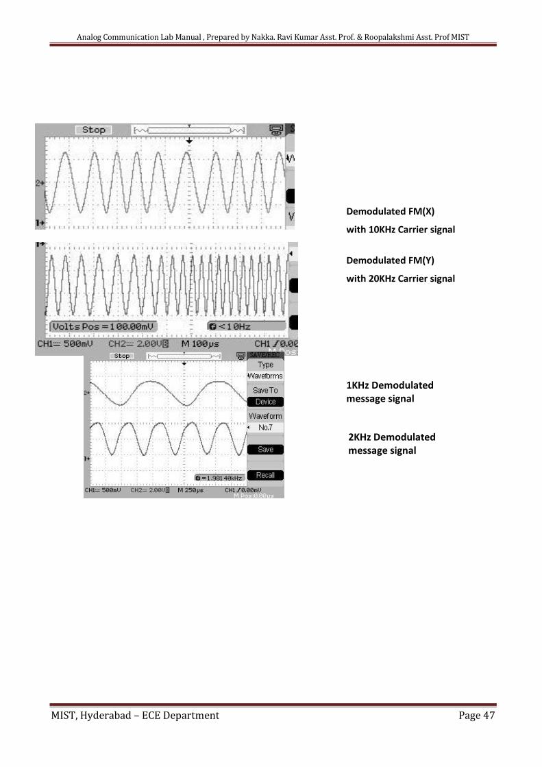
Demodulated FM(X)
with 10KHz Carrier signal
Demodulated FM(Y)
with 20KHz Carrier signal
1KHz Demodulated message signal
2KHz Demodulated message signal
Analog Communication Lab Manual , Prepared by Nakka. Ravi Kumar Asst. Prof. & Roopalakshmi Asst. Prof MIST
MIST, Hyderabad – ECE Department Page 48
EXPERIMENT – 9
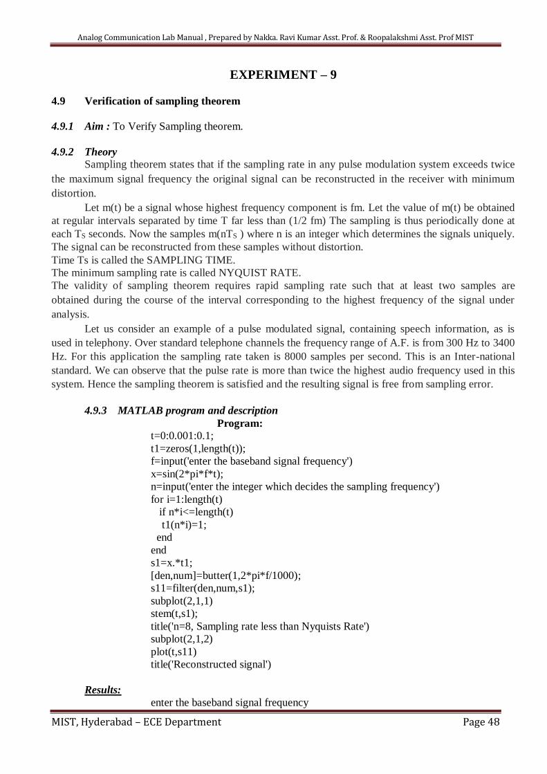
4.9 Verification of sampling theorem
4.9.1 Aim : To Verify Sampling theorem.
4.9.2 Theory
Sampling theorem states that if the sampling rate in any pulse modulation system exceeds twice
the maximum signal frequency the original signal can be reconstructed in the receiver with minimum
distortion.
Let m(t) be a signal whose highest frequency component is fm. Let the value of m(t) be obtained
at regular intervals separated by time T far less than (1/2 fm) The sampling is thus periodically done at
each TS seconds. Now the samples m(nTS ) where n is an integer which determines the signals uniquely.
The signal can be reconstructed from these samples without distortion.
Time Ts is called the SAMPLING TIME.
The minimum sampling rate is called NYQUIST RATE.
The validity of sampling theorem requires rapid sampling rate such that at least two samples are
obtained during the course of the interval corresponding to the highest frequency of the signal under
analysis.
Let us consider an example of a pulse modulated signal, containing speech information, as is
used in telephony. Over standard telephone channels the frequency range of A.F. is from 300 Hz to 3400
Hz. For this application the sampling rate taken is 8000 samples per second. This is an Inter-national
standard. We can observe that the pulse rate is more than twice the highest audio frequency used in this
system. Hence the sampling theorem is satisfied and the resulting signal is free from sampling error.
4.9.3 MATLAB program and description
Program:
t=0:0.001:0.1;
t1=zeros(1,length(t));
f=input('enter the baseband signal frequency')
x=sin(2*pi*f*t);
n=input('enter the integer which decides the sampling frequency')
for i=1:length(t)
if n*i<=length(t)
t1(n*i)=1;
end
end
s1=x.*t1;
[den,num]=butter(1,2*pi*f/1000);
s11=filter(den,num,s1);
subplot(2,1,1)
stem(t,s1);
title('n=8, Sampling rate less than Nyquists Rate')
subplot(2,1,2)
plot(t,s11)
title('Reconstructed signal')
Results:
enter the baseband signal frequency
Analog Communication Lab Manual , Prepared by Nakka. Ravi Kumar Asst. Prof. & Roopalakshmi Asst. Prof MIST
MIST, Hyderabad – ECE Department Page 49
f =10
enter the integer which decides the sampling frequency
n =8
enter the baseband signal frequency
f =10
enter the integer which decides the sampling frequency
n = 2
0 0.01 0.02 0.03 0.04 0.05 0.06 0.07 0.08 0.09 0.1-1
-0.5
0
0.5
1n=8, Sampling rate less than Nyquists Rate
0 0.01 0.02 0.03 0.04 0.05 0.06 0.07 0.08 0.09 0.1-0.2
-0.1
0
0.1
0.2Reconstructed signal
0 0.01 0.02 0.03 0.04 0.05 0.06 0.07 0.08 0.09 0.1-1
-0.5
0
0.5
1n=2, Sampling rate more than Nyquists Rate
0 0.01 0.02 0.03 0.04 0.05 0.06 0.07 0.08 0.09 0.1-0.5
0
0.5Reconstructed signal
Analog Communication Lab Manual , Prepared by Nakka. Ravi Kumar Asst. Prof. & Roopalakshmi Asst. Prof MIST
MIST, Hyderabad – ECE Department Page 50
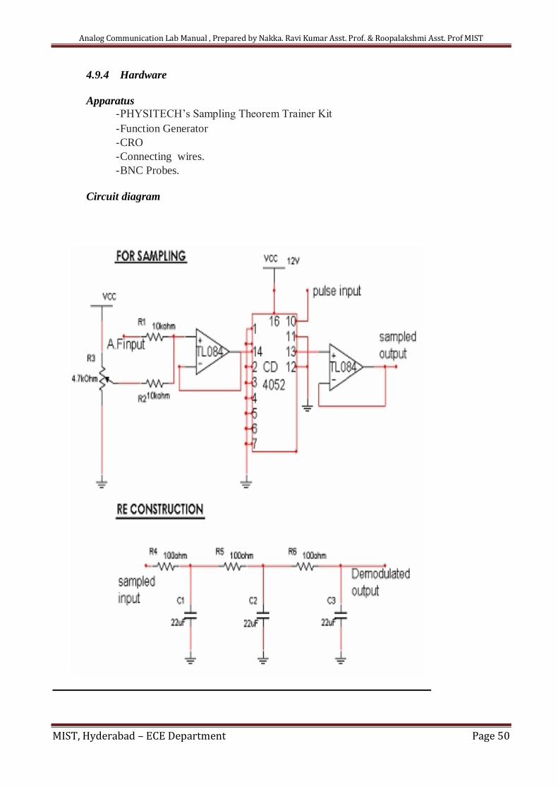
4.9.4 Hardware
Apparatus
- PHYSITECH’s Sampling Theorem Trainer Kit - Function Generator - CRO - Connecting wires. - BNC Probes.
Circuit diagram
Analog Communication Lab Manual , Prepared by Nakka. Ravi Kumar Asst. Prof. & Roopalakshmi Asst. Prof MIST
MIST, Hyderabad – ECE Department Page 51
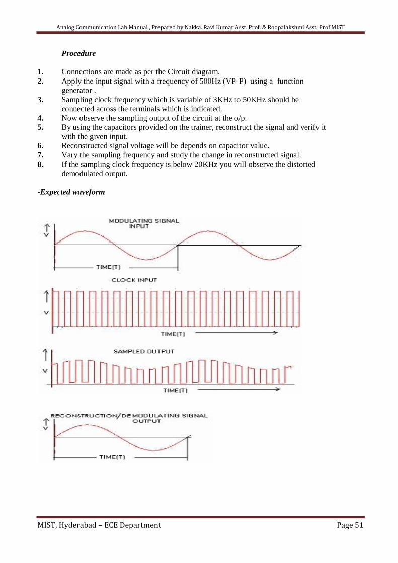
Procedure
1. Connections are made as per the Circuit diagram.
2. Apply the input signal with a frequency of 500Hz (VP-P) using a function
generator .
3. Sampling clock frequency which is variable of 3KHz to 50KHz should be
connected across the terminals which is indicated.
4. Now observe the sampling output of the circuit at the o/p.
5. By using the capacitors provided on the trainer, reconstruct the signal and verify it
with the given input.
6. Reconstructed signal voltage will be depends on capacitor value.
7. Vary the sampling frequency and study the change in reconstructed signal.
8. If the sampling clock frequency is below 20KHz you will observe the distorted
demodulated output.
-Expected waveform
Analog Communication Lab Manual , Prepared by Nakka. Ravi Kumar Asst. Prof. & Roopalakshmi Asst. Prof MIST
MIST, Hyderabad – ECE Department Page 52
EXPERIMENT - 10
4.10 Pulse Amplitude modulation and demodulation
4.10.1 AIM: To study the Pulse Amplitude modulation and de-modulation and their waveforms.
4.10.2 Theory
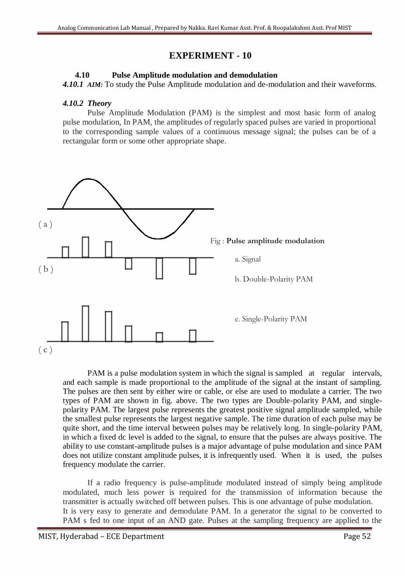
Pulse Amplitude Modulation (PAM) is the simplest and most basic form of analog
pulse modulation, In PAM, the amplitudes of regularly spaced pulses are varied in proportional
to the corresponding sample values of a continuous message signal; the pulses can be of a
rectangular form or some other appropriate shape.
( a )
Fig : Pulse amplitude modulation
a. Signal
( b ) b. Double-Polarity PAM
c. Single-Polarity PAM
( c )
PAM is a pulse modulation system in which the signal is sampled at regular intervals, and each sample is made proportional to the amplitude of the signal at the instant of sampling. The pulses are then sent by either wire or cable, or else are used to modulate a carrier. The two types of PAM are shown in fig. above. The two types are Double-polarity PAM, and single-polarity PAM. The largest pulse represents the greatest positive signal amplitude sampled, while the smallest pulse represents the largest negative sample. The time duration of each pulse may be quite short, and the time interval between pulses may be relatively long. In single-polarity PAM, in which a fixed dc level is added to the signal, to ensure that the pulses are always positive. The ability to use constant-amplitude pulses is a major advantage of pulse modulation and since PAM does not utilize constant amplitude pulses, it is infrequently used. When it is used, the pulses frequency modulate the carrier.
If a radio frequency is pulse-amplitude modulated instead of simply being amplitude
modulated, much less power is required for the transmission of information because the
transmitter is actually switched off between pulses. This is one advantage of pulse modulation.
It is very easy to generate and demodulate PAM. In a generator the signal to be converted to
PAM s fed to one input of an AND gate. Pulses at the sampling frequency are applied to the
Analog Communication Lab Manual , Prepared by Nakka. Ravi Kumar Asst. Prof. & Roopalakshmi Asst. Prof MIST
MIST, Hyderabad – ECE Department Page 53
other input of the AND gate to open it during the wanted time intervals. The output of the gate
then consists of pulses at the sampling rate, equal in amplitude to the signal voltage at each
instant. The pulses are then passed through a pulse-shaping network, which gives them flat tops.
Frequency modulation is then employed, so that the system becomes PAM-FM.
In the receiver, the pulses are first recovered with a standard FM de-modulator. They are
then fed to an ordinary diode detector, which is followed by a low-pass filter. If the cutoff
frequency of this filter is high enough to pass the highest signal frequency, but low enough to
remove the Sampling frequency ripple, an undistorted replica of the original signal is
reproduced.
4.10.3 MATLAB program and description
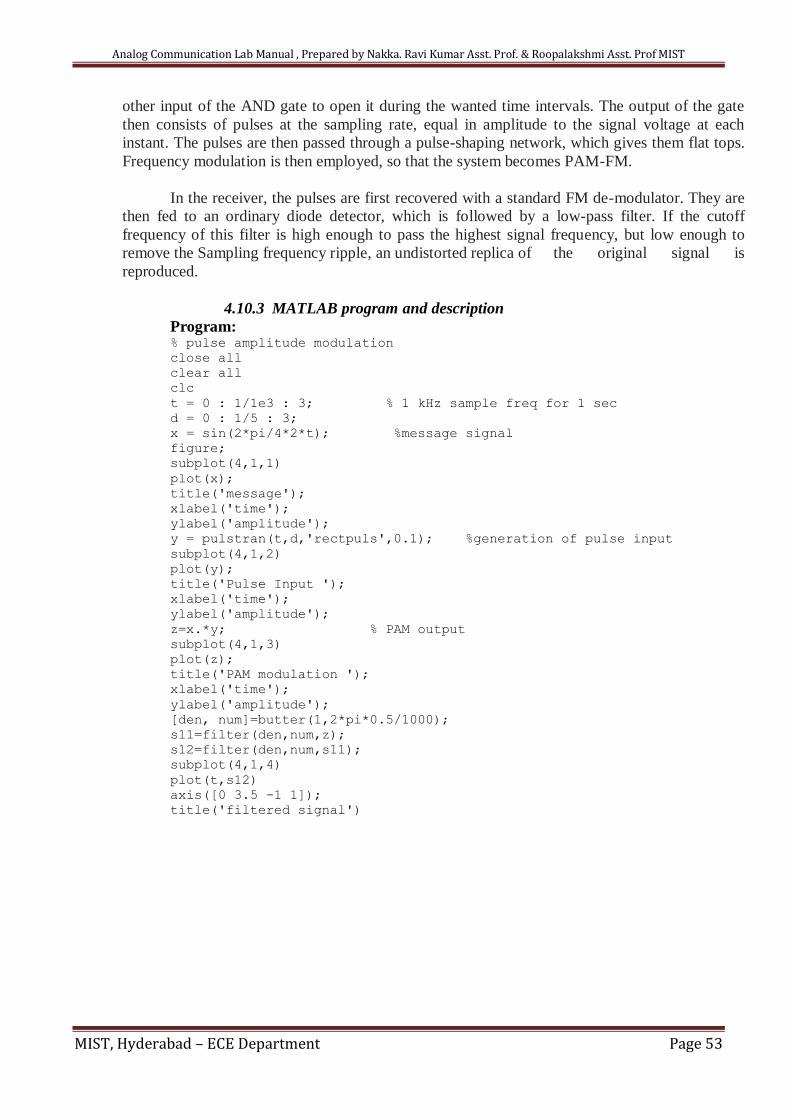
Program: % pulse amplitude modulation close all clear all clc t = 0 : 1/1e3 : 3; % 1 kHz sample freq for 1 sec d = 0 : 1/5 : 3; x = sin(2*pi/4*2*t); %message signal figure; subplot(4,1,1) plot(x); title('message'); xlabel('time'); ylabel('amplitude'); y = pulstran(t,d,'rectpuls',0.1); %generation of pulse input subplot(4,1,2) plot(y); title('Pulse Input '); xlabel('time'); ylabel('amplitude'); z=x.*y; % PAM output subplot(4,1,3) plot(z); title('PAM modulation '); xlabel('time'); ylabel('amplitude'); [den, num]=butter(1,2*pi*0.5/1000); s11=filter(den,num,z); s12=filter(den,num,s11); subplot(4,1,4) plot(t,s12) axis([0 3.5 -1 1]); title('filtered signal')
Analog Communication Lab Manual , Prepared by Nakka. Ravi Kumar Asst. Prof. & Roopalakshmi Asst. Prof MIST
MIST, Hyderabad – ECE Department Page 54
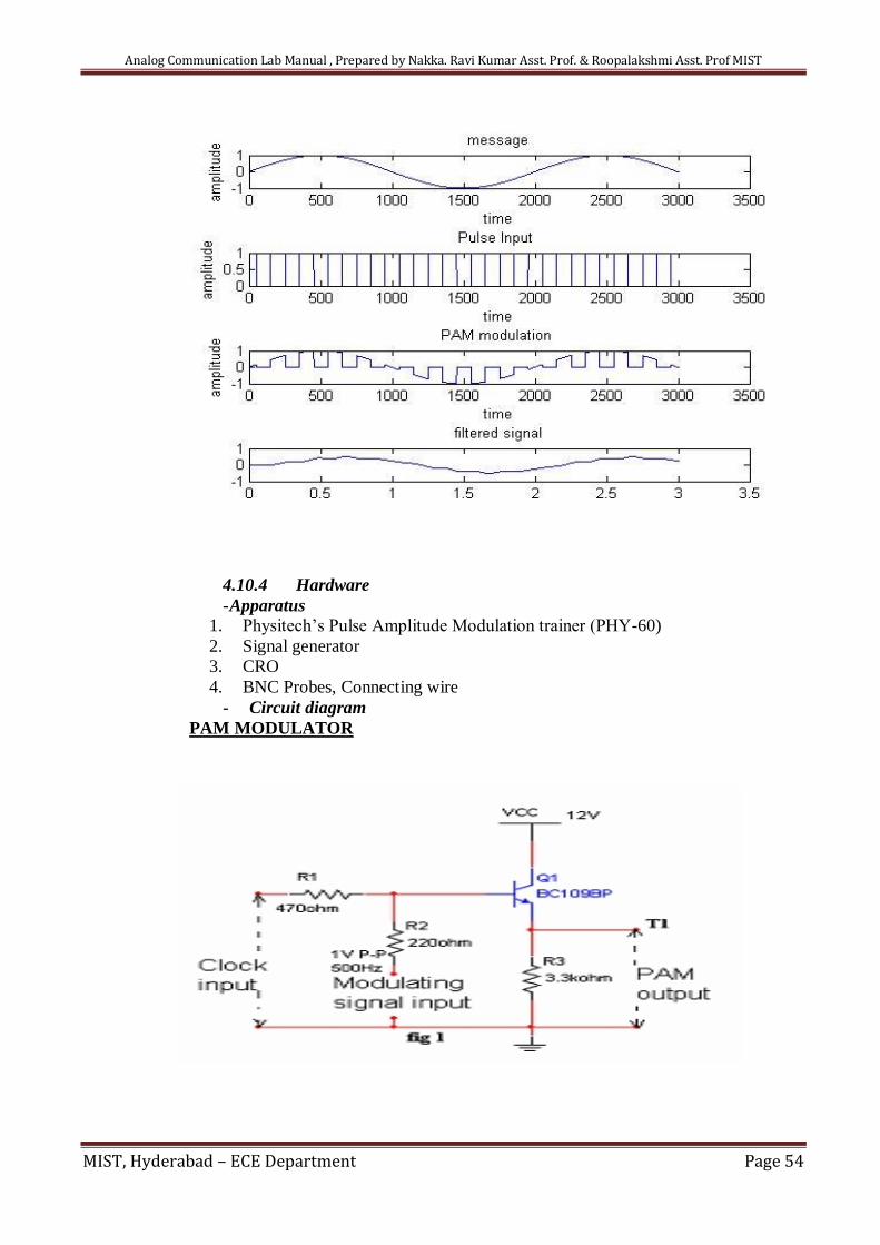
4.10.4 Hardware
- Apparatus
1. Physitech’s Pulse Amplitude Modulation trainer (PHY-60)
2. Signal generator
3. CRO
4. BNC Probes, Connecting wire
- Circuit diagram
PAM MODULATOR
Analog Communication Lab Manual , Prepared by Nakka. Ravi Kumar Asst. Prof. & Roopalakshmi Asst. Prof MIST
MIST, Hyderabad – ECE Department Page 55
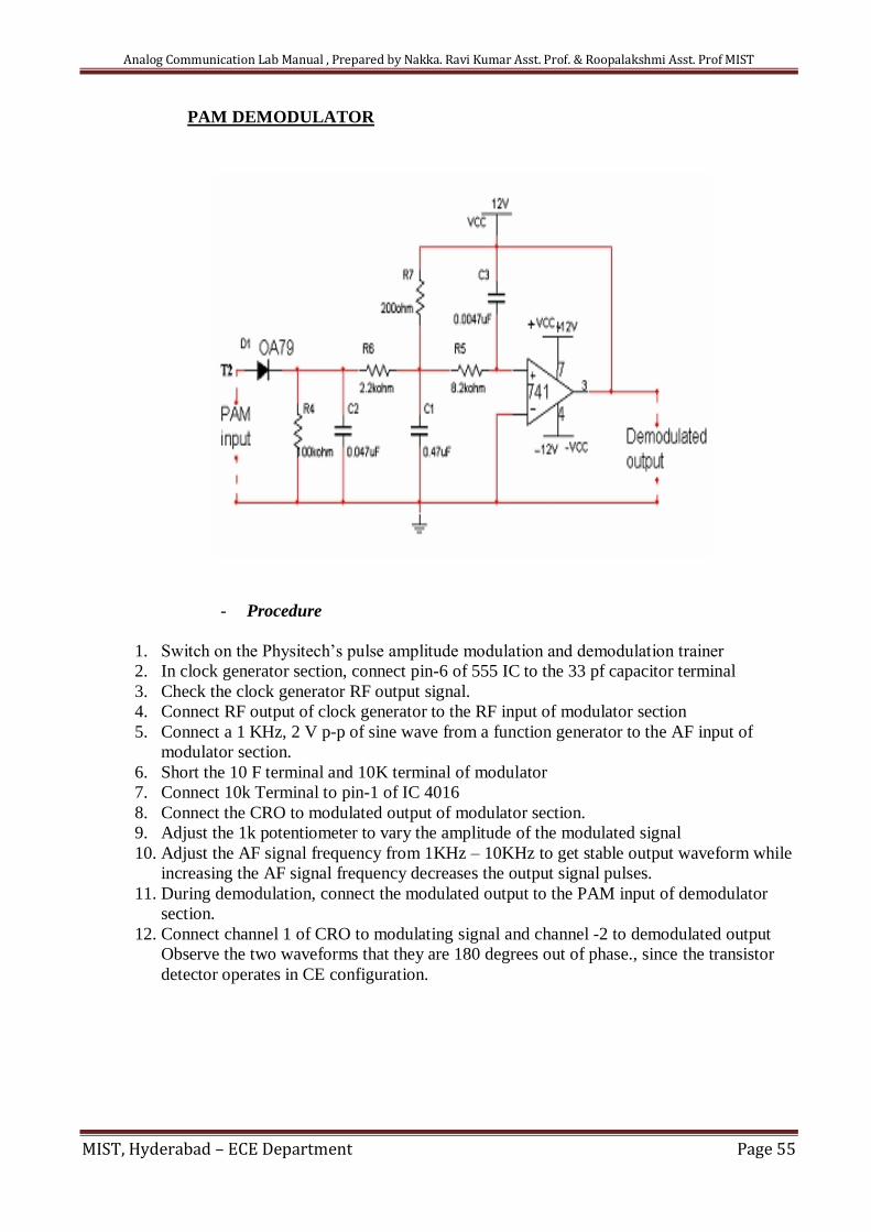
PAM DEMODULATOR
- Procedure
1. Switch on the Physitech’s pulse amplitude modulation and demodulation trainer
2. In clock generator section, connect pin-6 of 555 IC to the 33 pf capacitor terminal
3. Check the clock generator RF output signal.
4. Connect RF output of clock generator to the RF input of modulator section
5. Connect a 1 KHz, 2 V p-p of sine wave from a function generator to the AF input of
modulator section.
6. Short the 10 F terminal and 10K terminal of modulator
7. Connect 10k Terminal to pin-1 of IC 4016
8. Connect the CRO to modulated output of modulator section.
9. Adjust the 1k potentiometer to vary the amplitude of the modulated signal
10. Adjust the AF signal frequency from 1KHz – 10KHz to get stable output waveform while
increasing the AF signal frequency decreases the output signal pulses.
11. During demodulation, connect the modulated output to the PAM input of demodulator
section.
12. Connect channel 1 of CRO to modulating signal and channel -2 to demodulated output
Observe the two waveforms that they are 180 degrees out of phase., since the transistor
detector operates in CE configuration.
Analog Communication Lab Manual , Prepared by Nakka. Ravi Kumar Asst. Prof. & Roopalakshmi Asst. Prof MIST
MIST, Hyderabad – ECE Department Page 56
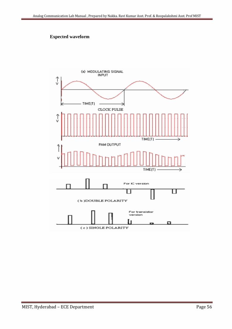
Expected waveform
Analog Communication Lab Manual , Prepared by Nakka. Ravi Kumar Asst. Prof. & Roopalakshmi Asst. Prof MIST
MIST, Hyderabad – ECE Department Page 57
EXPERIMENT – 11
4.11 Pulse width modulation and demodulation
4.11.1 AIM : To study the Pulse Width Modulation (PWM) and Demodulation process and
record the corresponding waveforms
4.11.2 Theory
The Pulse-width modulation of PTM is also called as Pulse-duration
modulation (PDM), or pulse length modulation (PLM). In this modulation, the pulses
have a constant amplitude and a variable time duration. The time duration (or width)
of each pulse is proportional to the instantaneous amplitude of the modulating signal.
In this system, as shown in fig. below, we have a fixed amplitude and starting time of
watch pulse, but the width of each pulse is made proportional to the amplitude of the
signal at that instant.
In this case, the narrowest pulse represents the most negative sample of the
original signal and the widest pulse represents the most positive sample.
When PDM is applied to radio transmission, the carrier frequency has
constant amplitude, and the transmitter on time is carefully controlled in some
circumstances, PDM can be more accurate than PAM. One example of this is in
magnetic tape recording, where pulse widths can be recorded and reproduced with
less error than pulse amplitudes.
PWM or PPM are not used in telephony. To use PWM or PPM in such an
application, we have to ensure that full scale modulation will not cause a pulse from
one message signal to enter a time slot belonging to another message signal. This
restriction results in a wasteful use of time space in telephone systems that are
characterized by high peak factors.
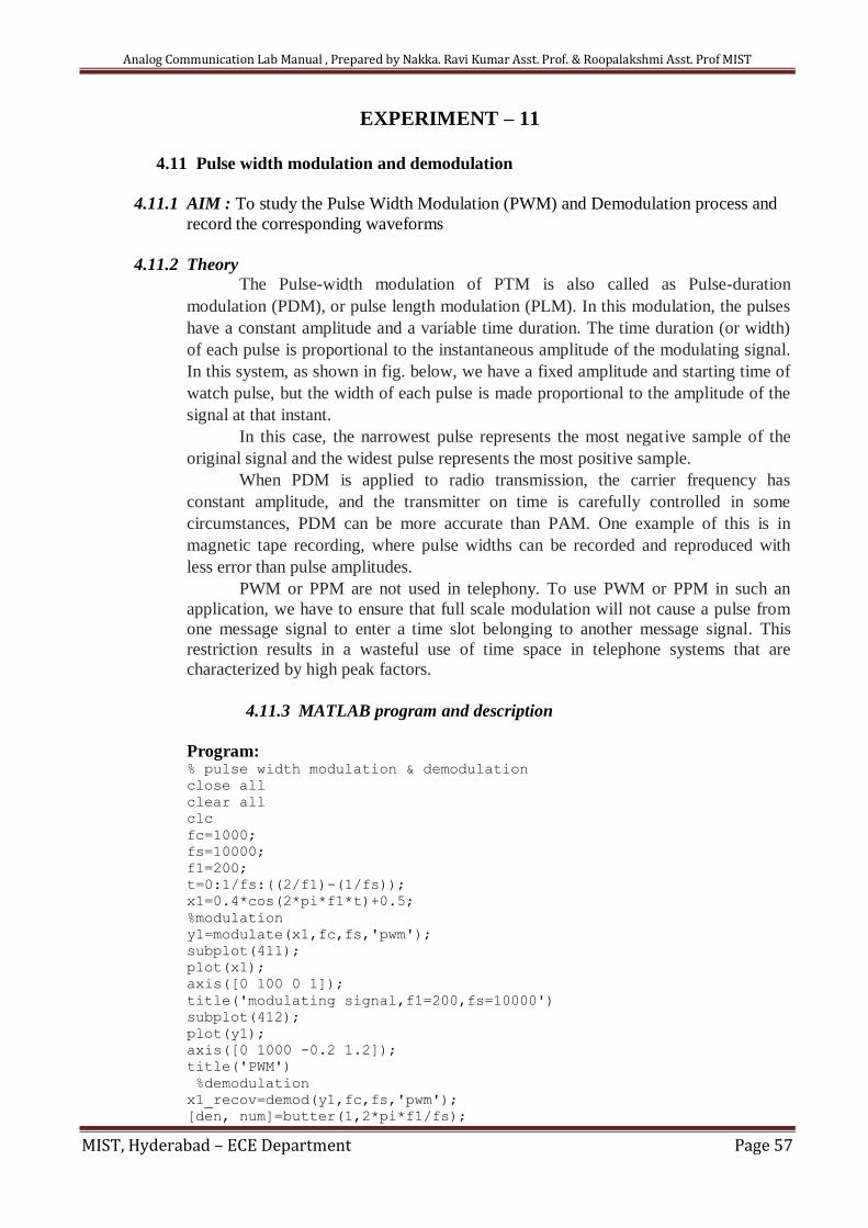
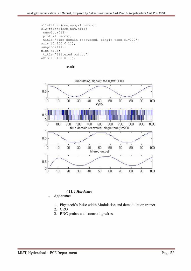
4.11.3 MATLAB program and description
Program: % pulse width modulation & demodulation close all clear all clc fc=1000; fs=10000; f1=200; t=0:1/fs:((2/f1)-(1/fs)); x1=0.4*cos(2*pi*f1*t)+0.5; %modulation y1=modulate(x1,fc,fs,'pwm'); subplot(411); plot(x1); axis([0 100 0 1]); title('modulating signal,f1=200,fs=10000') subplot(412); plot(y1); axis([0 1000 -0.2 1.2]); title('PWM') %demodulation x1_recov=demod(y1,fc,fs,'pwm'); [den, num]=butter(1,2*pi*f1/fs);
Analog Communication Lab Manual , Prepared by Nakka. Ravi Kumar Asst. Prof. & Roopalakshmi Asst. Prof MIST
MIST, Hyderabad – ECE Department Page 58
s11=filter(den,num,x1_recov); s12=filter(den,num,s11); subplot(413); plot(x1_recov); title('time domain recovered, single tone,f1=200')
axis([0 100 0 1]); subplot(414); plot(s12);
title('filtered output') axis([0 100 0 1]);
result:
4.11.4 Hardware
- Apparatus
1. Physitech’s Pulse width Modulation and demodulation trainer
2. CRO
3. BNC probes and connecting wires.
Analog Communication Lab Manual , Prepared by Nakka. Ravi Kumar Asst. Prof. & Roopalakshmi Asst. Prof MIST
MIST, Hyderabad – ECE Department Page 59
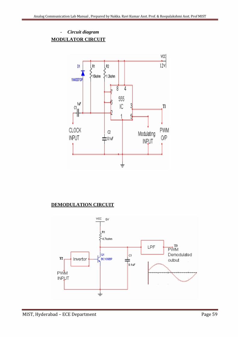
- Circuit diagram
MODULATOR CIRCUIT
DEMODULATION CIRCUIT
Analog Communication Lab Manual , Prepared by Nakka. Ravi Kumar Asst. Prof. & Roopalakshmi Asst. Prof MIST
MIST, Hyderabad – ECE Department Page 60
- Procedure
1. Switch on Physitech’s pulse width modulation and demodulation trainer
2. Connect the Clk O/P to the Clk I/P terminal PWM modulation.
3. Connect the AF O/P to AF I/P terminal of PWM modulator
4. Observe the PWM O/P at pin-3 of 555 IC on CRO
5. By varying frequency and amplitude of the modulating signal, observe
the corresponding change in the width of the output pulses.
6. During demodulation, connect the PWM O/P of PWM modulation to the
PWM I/P of PWM demodulation.
7. Observe the demodulated output at AF O/P of PWM demodulation on
CRO.
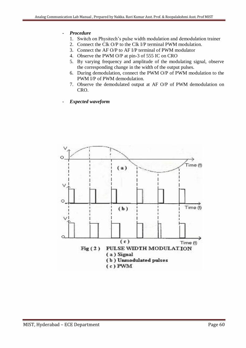
- Expected waveform
Analog Communication Lab Manual , Prepared by Nakka. Ravi Kumar Asst. Prof. & Roopalakshmi Asst. Prof MIST
MIST, Hyderabad – ECE Department Page 61
EXPERIMENT - 12
4.12 Pulse position modulation and demodulation
4.12.1 AIM : To study the Pulse Position Modulation (PPM) and demodulation process
and record corresponding waveforms.
4.12.2 Theory
Pulse position modulation (PPM) is more efficient than PAM or PDM for
radio transmission. In PPM all pulses have the same constant amplitude and narrow
pulse width. The position in time of the pulses is made to vary in proportion to the
amplitude of the modulating signal
The simplest modulation process for pulse position modulation is a PDM
system with the addition of a monostable multivibrator. The monostable is arranged
so that it is triggered by the trailing edges of the PDM pulses. Thus, the monostable
output is a series of constant-width, constant amplitude pulses which vary in position
according to the original signal a m p l i t u d e .
4.12.3 MATLAB program and description
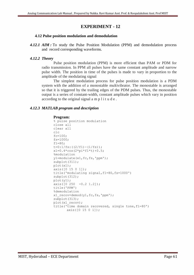
Program: % pulse position modulation close all clear all clc fc=100; fs=1000; f1=80; t=0:1/fs:((2/f1)-(1/fs)); x1=0.4*cos(2*pi*f1*t)+0.5; %modulation y1=modulate(x1,fc,fs,'ppm'); subplot(311); plot(x1); axis([0 15 0 1]); title('modulating signal,f1=80,fs=1000') subplot(312); plot(y1); axis([0 250 -0.2 1.2]); title('PPM') %demodulation x1_recov=demod(y1,fc,fs,'ppm'); subplot(313); plot(x1_recov); title('time domain recovered, single tone,f1=80')
axis([0 15 0 1]);
Analog Communication Lab Manual , Prepared by Nakka. Ravi Kumar Asst. Prof. & Roopalakshmi Asst. Prof MIST
MIST, Hyderabad – ECE Department Page 62
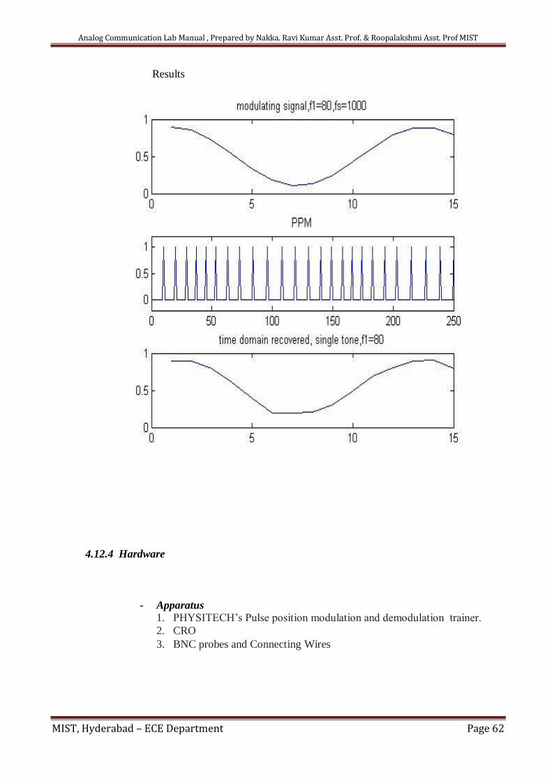
Results
4.12.4 Hardware
- Apparatus
1. PHYSITECH’s Pulse position modulation and demodulation trainer.
2. CRO 3. BNC probes and Connecting Wires
Analog Communication Lab Manual , Prepared by Nakka. Ravi Kumar Asst. Prof. & Roopalakshmi Asst. Prof MIST
MIST, Hyderabad – ECE Department Page 63
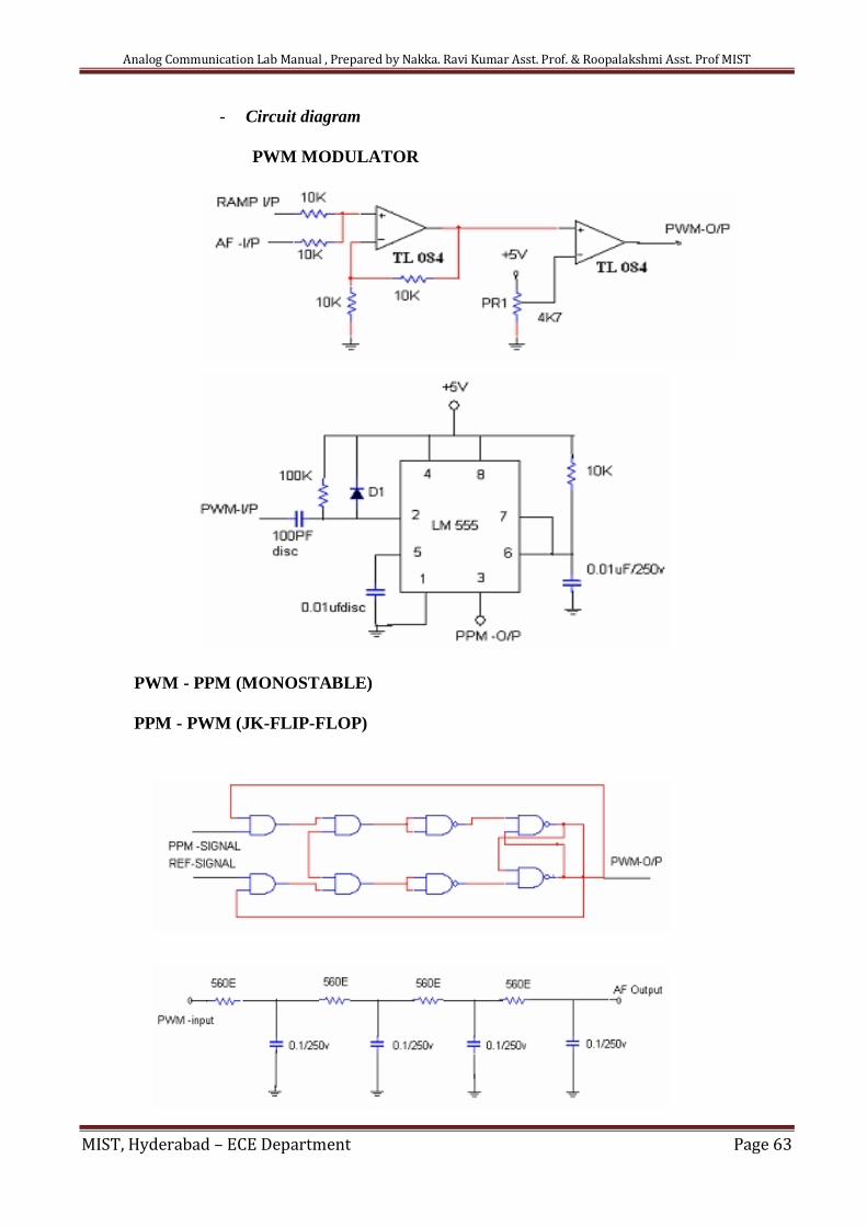
- Circuit diagram
PWM MODULATOR
PWM - PPM (MONOSTABLE)
PPM - PWM (JK-FLIP-FLOP)
Analog Communication Lab Manual , Prepared by Nakka. Ravi Kumar Asst. Prof. & Roopalakshmi Asst. Prof MIST
MIST, Hyderabad – ECE Department Page 64
PWM DEMODULATOR
- Procedure
1. Switch on PHYSITECH’s PPM modulator and demodulator trainer.
2 . Connect the Clk O/P to the Pin 2 of 555 IC.
3 . Connect the AF O/P to the pin 5 of 555 IC.
4 . Observe the PPM O/P at pin 3 of second IC 555 on CRO.
5 . Connect the PPM O/P to the PPM I/P of PPM demodulation.
6 . Observe the demodulated O/P on CRO
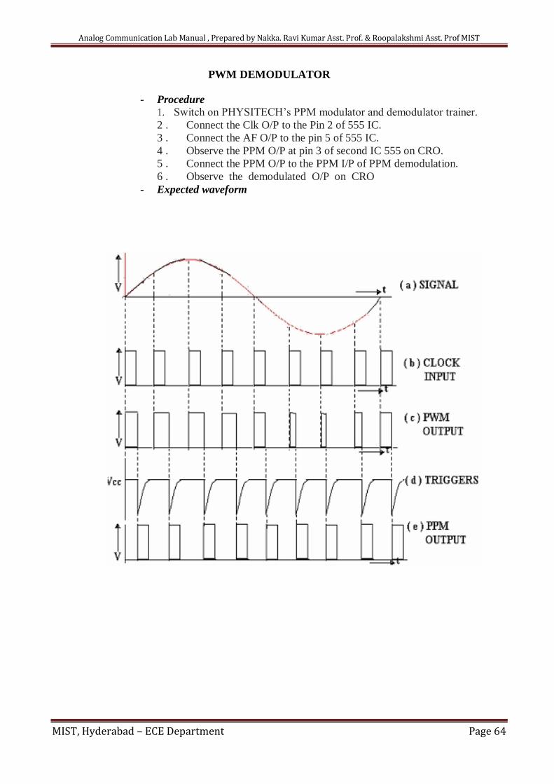
- Expected waveform
Analog Communication Lab Manual , Prepared by Nakka. Ravi Kumar Asst. Prof. & Roopalakshmi Asst. Prof MIST
MIST, Hyderabad – ECE Department Page 65
EXPERIMENT-13
4.13 Frequency synthesizer
4.13.1 AIM: To study the operation of frequency synthesizer using PLL
4.13.2 Theory
Synthesizer is an equipment capable of generating a very large number of
extremely stable frequencies with in same range of design ,while employing only
one single stable source .The required frequency range in most synthesizers now a
days is obtained from a variable voltage controller oscillator(vco),whose output is
corrected by comparison with that of a reference source. This in built source is
virtually a direct synthesizer.
There are two methods by which frequency multiplication can be achieved
by using LM565 IC 1.locking to the harmonic of the input signal. 2.inclusion of a digital frequency divider or counter in loop between the
VCO and phase comparator. The first method is simplest, and can be achieved by setting the free running
frequency of the VCO to a multiple of the input frequency. A limitation of this
method is that the lock range decreases as successively higher and weaker harmonics
are used for locking .If the input frequency is to be constant with little tracking
required the loop can generally be locked to any one of the first five harmonics. For
higher orders of multiplication, a large lock range is desired for which the second
scheme is more desirable.
4.13.3 MATLAB program and description
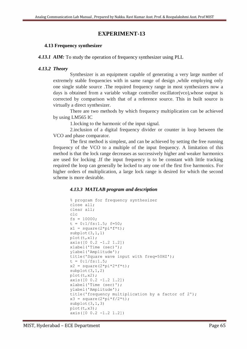
% program for frequency synthesizer close all; clear all; clc fs = 10000; t = 0:1/fs:1.5; f=50; x1 = square(2*pi*f*t); subplot(3,1,1) plot(t,x1); axis([0 0.2 -1.2 1.2]) xlabel('Time (sec)'); ylabel('Amplitude'); title('Square wave input with freq=50HZ'); t = 0:1/fs:1.5; x2 = square(2*pi*2*f*t); subplot(3,1,2) plot(t,x2); axis([0 0.2 -1.2 1.2]) xlabel('Time (sec)'); ylabel('Amplitude'); title('frequency multiplication by a factor of 2'); x3 = square(2*pi*f/2*t); subplot(3,1,3) plot(t,x3); axis([0 0.2 -1.2 1.2])
Analog Communication Lab Manual , Prepared by Nakka. Ravi Kumar Asst. Prof. & Roopalakshmi Asst. Prof MIST
MIST, Hyderabad – ECE Department Page 66
xlabel('Time (sec)'); ylabel('Amplitude'); title('frequency division by a factor of 2');
result
4.13.4 Hardware
- Apparatus
1. Physitech frequency synthesizer trainer (PHY-704).
2. Oscilloscope (OSC-5030, 30MHz ) or Equivalent.
3. BNC Probes (1:1/10:1, switch selectable).
4. Connecting wires
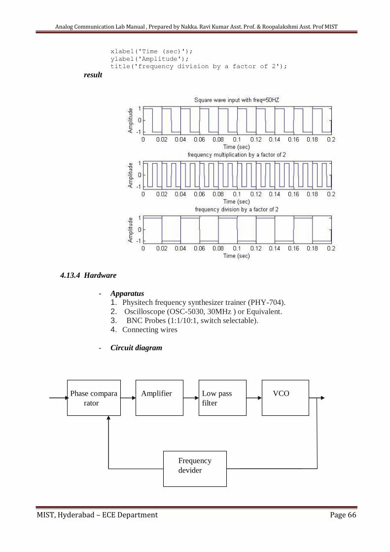
- Circuit diagram
Phase compara Amplifier Low pass VCO
rator filter
Frequency
devider
Analog Communication Lab Manual , Prepared by Nakka. Ravi Kumar Asst. Prof. & Roopalakshmi Asst. Prof MIST
MIST, Hyderabad – ECE Department Page 67
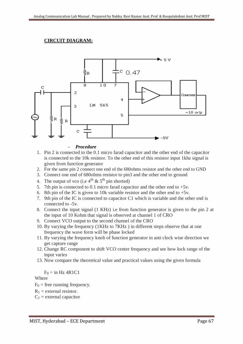
CIRCUIT DIAGRAM:
- Procedure
1. Pin 2 is connected to the 0.1 micro farad capacitor and the other end of the capacitor
is connected to the 10k resistor. To the other end of this resistor input 1khz signal is
given from function generator 2. For the same pin 2 connect one end of the 680ohms resistor and the other end to GND
3. Connect one end of 680ohms resistor to pin3 and the other end to ground
4. The output of vco (i.e 4th & 5th pin shorted)
5. 7th pin is connected to 0.1 micro farad capacitor and the other end to +5v.
6. 8th pin of the IC is given to 10k variable resistor and the other end to +5v.
7. 9th pin of the IC is connected to capacitor C1 which is variable and the other end is
connected to -5v.
8. Connect the input signal (1 KHz) i.e from function generator is given to the pin 2 at
the input of 10 Kohm that signal is observed at channel 1 of CRO
9. Connect VCO output to the second channel of the CRO
10. By varying the frequency (1KHz to 7KHz ) in different steps observe that at one
frequency the wave form will be phase locked
11. By varying the frequency knob of function generator in anti clock wise direction we
get capture range
12. Change RC component to shift VCO center frequency and see how lock range of the
input varies
13. Now compare the theoretical value and practical values using the given formula
F0 = in Hz 4R1C1
Where
F0 = free running frequency.
R1 = external resistor.
C1 = external capacitor
Analog Communication Lab Manual , Prepared by Nakka. Ravi Kumar Asst. Prof. & Roopalakshmi Asst. Prof MIST
MIST, Hyderabad – ECE Department Page 68
F = + { f 2
3.6x10³ C } 1/2
C 2
2p
Where
Fc = Capture Range.
C2 = the filter capacitor in farad.
FL = + 8fO Hz Where, Fl = Lock Range
VC
Expectedwaveforms:
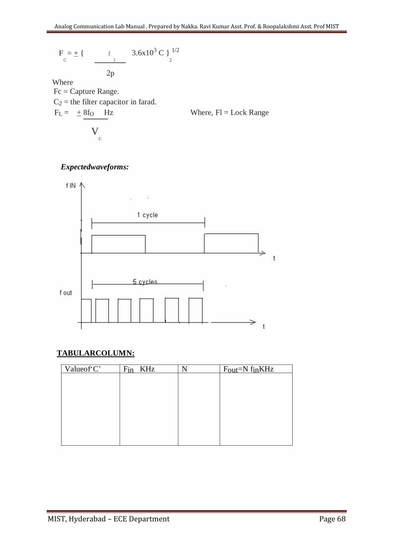
TABULARCOLUMN:
Valueof‘C’ Fin KHz N Fout=N finKHz
Analog Communication Lab Manual , Prepared by Nakka. Ravi Kumar Asst. Prof. & Roopalakshmi Asst. Prof MIST
MIST, Hyderabad – ECE Department Page 69
EXPERIMENT - 14
4.14 AGC characteristics
4.14.1 AIM : To Study the AGC characteristics of a Radio receiver
4.14.2 Theory
The main purpose of the receiver is to recreate the original message
signal from the degraded version of the transmitted signal after propagation
through the free space.
The Super Heterodyne Receiver :
The Basic receiver is shown in fig. (1) The first stage is a tuned RF
amplifier, using two variable tuned circuits that track each other and the local
oscillator. The two tuned RF circuits form a band pass filter to pass the desired
RF signal frequency while blocking others. This stage acts to boost the weak
signal level from the antenna above the noise level to provide same signal
selectivity and to prevent other channel signal to pass through.
The output signal from the amplifier is fed to one input of the mixer
circuit and the local oscillator signal to the other. The local oscillator is
variable tuned so as to track the incoming signal frequencies.
The mixer output (the difference frequency for down-conversion) is
fed to multistage tuned. IF amplifiers, which are fixed-tune and provided with
sufficient selectivity to reject adjacent channel signals. The output from the IF
amplifier chain is fed to the detector circuit. Where the audio signal is
extracted from the IF signal or demodulated. The detector also provides
signals for automatic gain control (AGC). The AGC signal is used as a bias
signal to reduce the gain of the RF and the IF amplifiers to prevent detector
overload. AGC is a system means of which the overall gain of a radio receiver
is varied automatically with the changing strength of the received signal to to
keep the output substantially constant.
The audio signal from the detector is passed through a low pass filter
to remove unwanted high frequency components and then through a volume
control to an audio amplifier. The audio amplifier is usually one low-level
audio stage followed by a power amplifier and a speaker. The gain required in the RF and IF amplifier chain of the receiver
depends on the required input and output. The input is the minimum variable
signal level to be presented at the antenna terminals. The output is the
minimum signal level at the input of the detector required to make the detector
perform satisfactorily . In this trainer we used Radio receiver IC 1610S which
is having in-built RF amplifier , Local oscillator, a mixer, IF amplifiers and
AGC detector, audio amplifier to drive a speaker.
Analog Communication Lab Manual , Prepared by Nakka. Ravi Kumar Asst. Prof. & Roopalakshmi Asst. Prof MIST
MIST, Hyderabad – ECE Department Page 70
4.14.3 MATLAB program and description
Program: % program for AGC close all; clear all; clc; A=input('enter the carrier signal peak') % 1 B=input('enter the baseband signal peak') % 0.25 f1=input('enter the baseband signal frequency') % 10 f2=input('enter the carrier signal frequency') % 100 fs=input('enter the sampling frequency') % 1000 t=0:0.001:1; M=cos(2*pi*f1*t); N=cos(2*pi*f2*t); m=B/A; O=A*(1+m*M).*N; O1=O; for i=1:length(t) if O1(i)<=0 O1(i)=0; end end [den,num]=butter(2,2*pi*f1/fs); M1=filter(den,num,O1); M11=filter(den,num,M1); M12=filter(den,num,M11); M13=filter(den,num,M12); Av=mean(M13); disp('AGC Bias is') disp(Av) M131=M13/Av; disp('Max of demodulated signal before Bias Correction is') disp(max(M13)) disp('Max of demodulated signal after Bias Correction is') disp(max(M131)) subplot(3,1,1) plot(t,O); title('Modulated Carrier') subplot(3,1,2) plot(t,M13) title('demodulated Signal') axis([0 1 0 4]) subplot(3,1,3) plot(t,M131) title('Demodulated signal after Bias correction') axis([0 1 0 4])
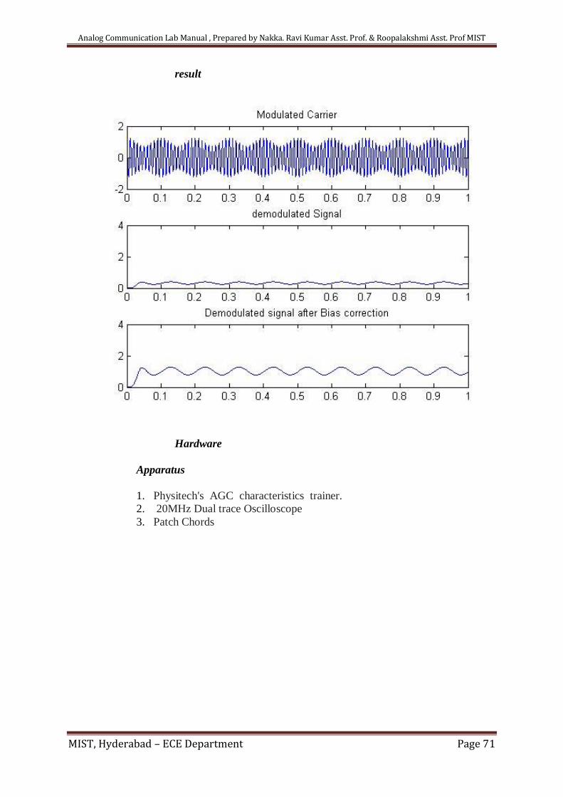
Analog Communication Lab Manual , Prepared by Nakka. Ravi Kumar Asst. Prof. & Roopalakshmi Asst. Prof MIST
MIST, Hyderabad – ECE Department Page 71
result
Hardware
Apparatus
1. Physitech's AGC characteristics trainer.
2. 20MHz Dual trace Oscilloscope
3. Patch Chords
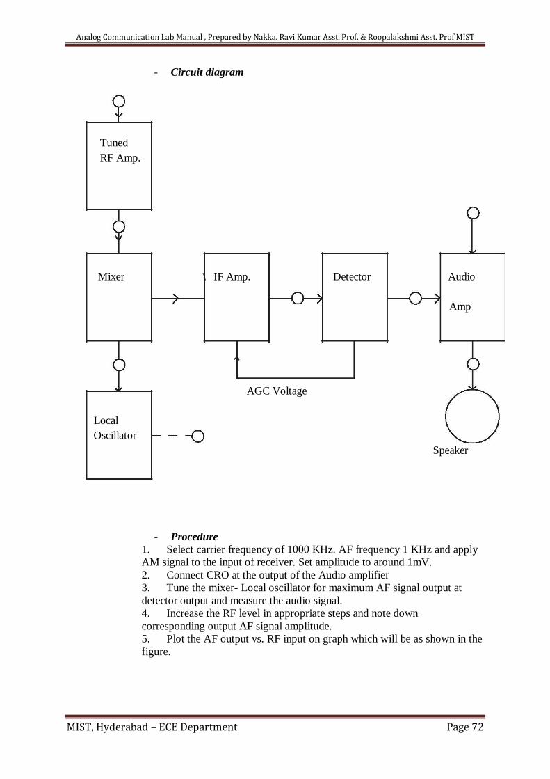
Analog Communication Lab Manual , Prepared by Nakka. Ravi Kumar Asst. Prof. & Roopalakshmi Asst. Prof MIST
MIST, Hyderabad – ECE Department Page 72
- Circuit diagram
Tuned
RF Amp.
Mixer \ IF Amp. Detector Audio
Amp
AGC Voltage
Local
Oscillator
Speaker
- Procedure
1. Select carrier frequency of 1000 KHz. AF frequency 1 KHz and apply
AM signal to the input of receiver. Set amplitude to around 1mV.
2. Connect CRO at the output of the Audio amplifier
3. Tune the mixer- Local oscillator for maximum AF signal output at
detector output and measure the audio signal.
4. Increase the RF level in appropriate steps and note down
corresponding output AF signal amplitude.
5. Plot the AF output vs. RF input on graph which will be as shown in the
figure.
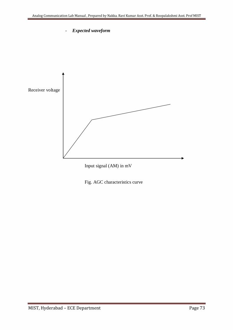
Analog Communication Lab Manual , Prepared by Nakka. Ravi Kumar Asst. Prof. & Roopalakshmi Asst. Prof MIST
MIST, Hyderabad – ECE Department Page 73
- Expected waveform
Receiver voltage
Input signal (AM) in mV
Fig. AGC characteristics curve

Analog Communication Lab Manual , Prepared by Nakka. Ravi Kumar Asst. Prof. & Roopalakshmi Asst. Prof MIST
MIST, Hyderabad – ECE Department Page 74
EXPERIMENT – 15
4.15 PLL
4.15.1 AIM : To study phase lock loop and its capture range, lock range and
free running VCO Frequency.
4.15.2 Theory
PLL has emerged as one of the fundamental building block in
electronic technology. It is used for the frequency multiplication,
FM stereo detector, FM demodulator, frequency shift keying decoders, local
oscillator in TV and FM tuner.
The block diagram of PLL is shown below.
fin fout
fout
The PLL consists of Phase detector, a LPF and a voltage controlled
oscillator. (VCO) connected together in the form a feedback system. The VCO
is a sinusoidal generator whose frequency is determined by a voltage applied
to it from an external source. In effect, any frequency modulator may serve as
a VCO.
The phase detector or comparator compares the input frequency, fin,
with feedback frequency, fout. The output of the phase detector is proportional
to the phase difference between fin and fout. The output voltage of the phase
detector is a DC voltage and therefore is often refers to as error voltage. The
output of the phase detector ios then applied to the LPF, which removes the
high frequency noise and produces a DC level. The DC level, intern is the
input to the VCO.
The output frequency of the VCO is directly proportional to the input
DC level . The VCO frequency is compared with the input frequencies and
adjusted until it is equal to the input frequency. In short, PLL keeps its out
frequency constant at the input frequency.
Phase detector Low pass
Filter
VCO
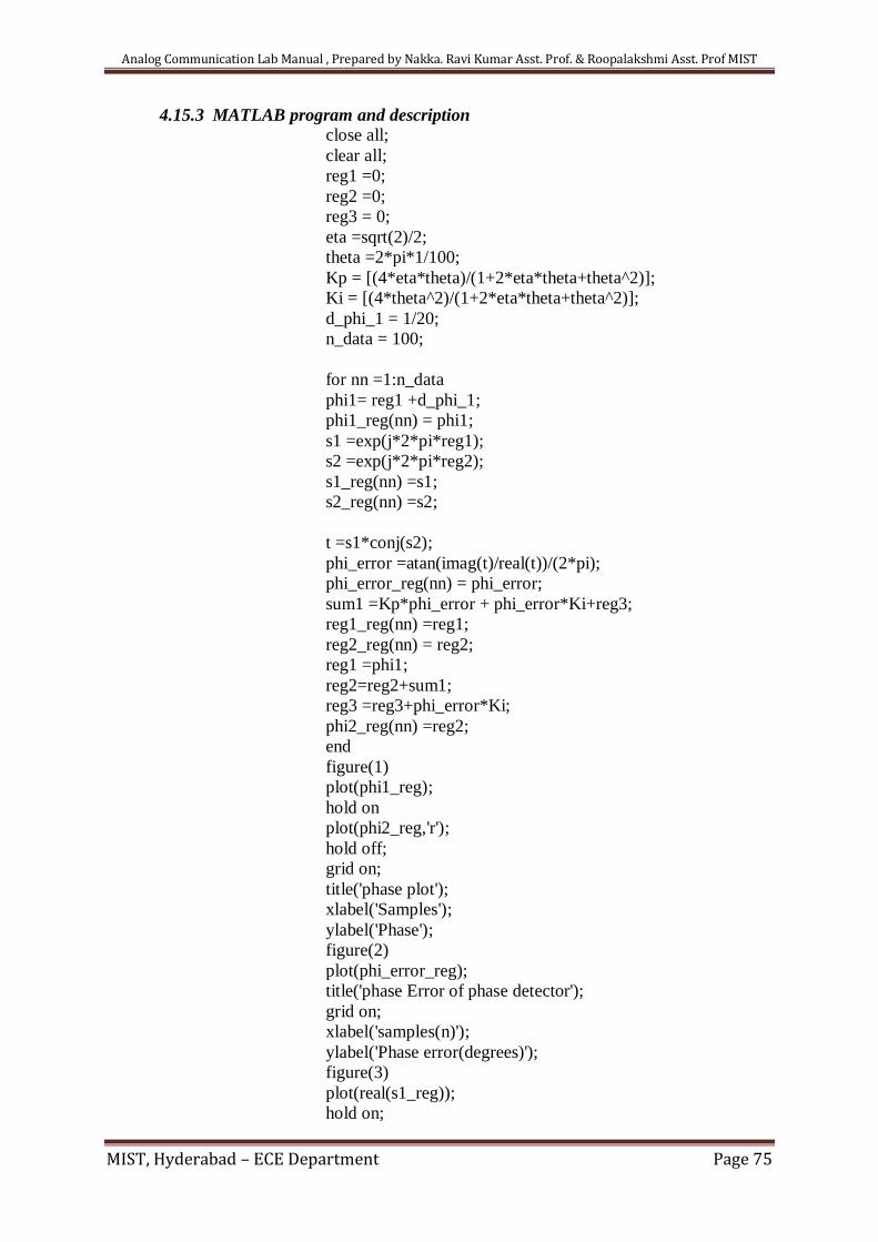
Analog Communication Lab Manual , Prepared by Nakka. Ravi Kumar Asst. Prof. & Roopalakshmi Asst. Prof MIST
MIST, Hyderabad – ECE Department Page 75
4.15.3 MATLAB program and description
close all;
clear all;
reg1 =0;
reg2 =0;
reg3 = 0;
eta =sqrt(2)/2;
theta =2*pi*1/100;
Kp = [(4*eta*theta)/(1+2*eta*theta+theta^2)];
Ki = [(4*theta^2)/(1+2*eta*theta+theta^2)];
d_phi_1 = 1/20;
n_data = 100;
for nn =1:n_data
phi1= reg1 +d_phi_1;
phi1_reg(nn) = phi1;
s1 =exp(j*2*pi*reg1);
s2 =exp(j*2*pi*reg2);
s1_reg(nn) =s1;
s2_reg(nn) =s2;
t =s1*conj(s2);
phi_error =atan(imag(t)/real(t))/(2*pi);
phi_error_reg(nn) = phi_error;
sum1 =Kp*phi_error + phi_error*Ki+reg3;
reg1_reg(nn) =reg1;
reg2_reg(nn) = reg2;
reg1 =phi1;
reg2=reg2+sum1;
reg3 =reg3+phi_error*Ki;
phi2_reg(nn) =reg2;
end
figure(1)
plot(phi1_reg);
hold on
plot(phi2_reg,'r');
hold off;
grid on;
title('phase plot');
xlabel('Samples');
ylabel('Phase');
figure(2)
plot(phi_error_reg);
title('phase Error of phase detector');
grid on;
xlabel('samples(n)');
ylabel('Phase error(degrees)');
figure(3)
plot(real(s1_reg));
hold on;
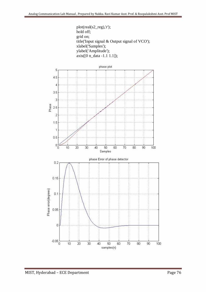
Analog Communication Lab Manual , Prepared by Nakka. Ravi Kumar Asst. Prof. & Roopalakshmi Asst. Prof MIST
MIST, Hyderabad – ECE Department Page 76
plot(real(s2_reg),'r');
hold off;
grid on;
title('Input signal & Output signal of VCO');
xlabel('Samples');
ylabel('Amplitude');
axis([0 n_data -1.1 1.1]);
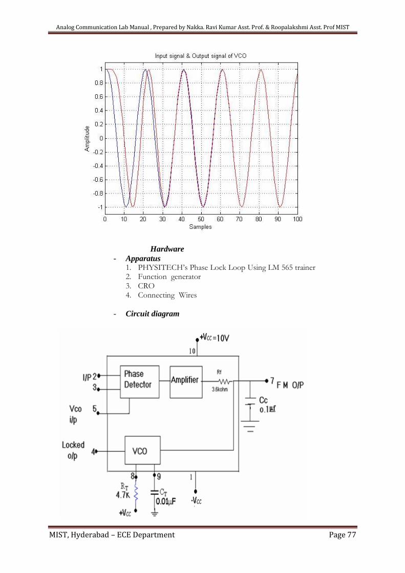
Analog Communication Lab Manual , Prepared by Nakka. Ravi Kumar Asst. Prof. & Roopalakshmi Asst. Prof MIST
MIST, Hyderabad – ECE Department Page 77
Hardware
- Apparatus 1. PHYSITECH’s Phase Lock Loop Using LM 565 trainer 2. Function generator 3. CRO 4. Connecting Wires
- Circuit diagram

Analog Communication Lab Manual , Prepared by Nakka. Ravi Kumar Asst. Prof. & Roopalakshmi Asst. Prof MIST
MIST, Hyderabad – ECE Department Page 78
- Procedure
Free running frequency:
1. Switch on the trainer and measure the output of the regulated power supplies i.e.,
+12V and ±5V
2. Observe the output of the square wave generator-using oscilloscope and measure
the frequency range. The frequency range should be around 1KHz to 10KHz.
3. Calculate the free running frequency range of the circuit for different values of
timing capacitor and Rt.
4. Connect 0.1µF capacitor (CC) to the circuit and open the loop by removing short
between pin 4 and 5 . Measure the minimum and maximum free running frequencies
obtainable at the output of the PLL (Pin4)by varying the pot. Compare your results
with your calculation from step 3 (theoretical value). Simultaneously you can
observe the output signal using CRO.
Table 1: 1 Free running frequency Rt value(pot resistance
in Ohms)
Theoretical value
(frequency in KHz)
Practical value
(frequency in KHz)
Lock range:
5. Calculate the lock range of the circuit for a 5KHz free running frequency and
record in table 1.2.
6. Connect pins 4,5 with the help of springs and adjust potentiometer to get a free
running frequency of 5KHz . Connect square wave generator output to the input of
PLL circuit. Provide a 5KHz square signal of 1 Vpp approximately (make this input
frequency as close to the Vcc frequency as possible).
7. Observe the input & Output of the PLL.
8. Observe the input and output frequencies while slowly increasing the frequency of
the square wave at the input. For some range output and input are equal (This is known
as lock Range and PLL is said to be in lock with the input signal). Record the
frequency at which the PLL breaks lock. (Output frequency of the PLL will be
around VCO frequency and in oscilloscope you will see a jittery waveform when it
breaks lock instead of clean square wave). This frequency is called as upper end of
the lock range and records this as F2.
9. Beginning at 5KHz, slowly decrease the frequency of the input and determine the
frequency at which the PLL breaks lock on the low end record it as F1
10. Find the lock range from F2 - F1 and compare with the theoretical values from
step5.
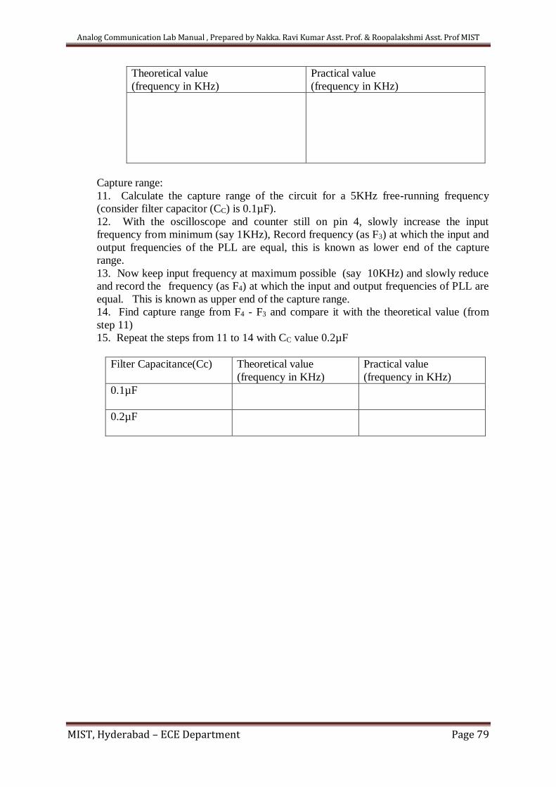
Analog Communication Lab Manual , Prepared by Nakka. Ravi Kumar Asst. Prof. & Roopalakshmi Asst. Prof MIST
MIST, Hyderabad – ECE Department Page 79
Theoretical value
(frequency in KHz)
Practical value
(frequency in KHz)
Capture range:
11. Calculate the capture range of the circuit for a 5KHz free-running frequency
(consider filter capacitor (CC) is 0.1µF).
12. With the oscilloscope and counter still on pin 4, slowly increase the input
frequency from minimum (say 1KHz), Record frequency (as F3) at which the input and
output frequencies of the PLL are equal, this is known as lower end of the capture
range.
13. Now keep input frequency at maximum possible (say 10KHz) and slowly reduce
and record the frequency (as F4) at which the input and output frequencies of PLL are
equal. This is known as upper end of the capture range.
14. Find capture range from F4 - F3 and compare it with the theoretical value (from
step 11)
15. Repeat the steps from 11 to 14 with CC value 0.2µF
Filter Capacitance(Cc)
Theoretical value
(frequency in KHz)
Practical value
(frequency in KHz)
0.1µF
0.2µF


![MN67175 ENG 1 - ADFWeb.comVmin Vmax Vmin Vmax 8V 24V 12V 35V Consumption at 24V DC: Device Consumption [W/VA] HD67175-xxx-A1 3.5 HD67175-xxx-B2 3.5 Caution: Not reverse the polarity](https://static.fdocuments.in/doc/165x107/5ea0f7ed5bfc5b663a081192/mn67175-eng-1-vmin-vmax-vmin-vmax-8v-24v-12v-35v-consumption-at-24v-dc-device.jpg)