Analog and Telecommunication Electronics · 2011-05-12 · 12/05/2011 - 4 ATLCE - D3 - © 2010 DDC...
79
12/05/2011 - 1 ATLCE - D3 - © 2010 DDC Politecnico di Torino - ICT School Analog and Telecommunication Electronics D3 - A/D converters » Error taxonomy » ADC parameters » Structures and taxonomy » Mixed converters » Origin of errors
Transcript of Analog and Telecommunication Electronics · 2011-05-12 · 12/05/2011 - 4 ATLCE - D3 - © 2010 DDC...
12/05/2011 - 1 ATLCE - D3 - © 2010 DDC
Politecnico di Torino - ICT School
Analog and Telecommunication Electronics
D3 - A/D converters
» Error taxonomy» ADC parameters» Structures and taxonomy» Mixed converters» Origin of errors
12/05/2011 - 2 ATLCE - D3 - © 2010 DDC
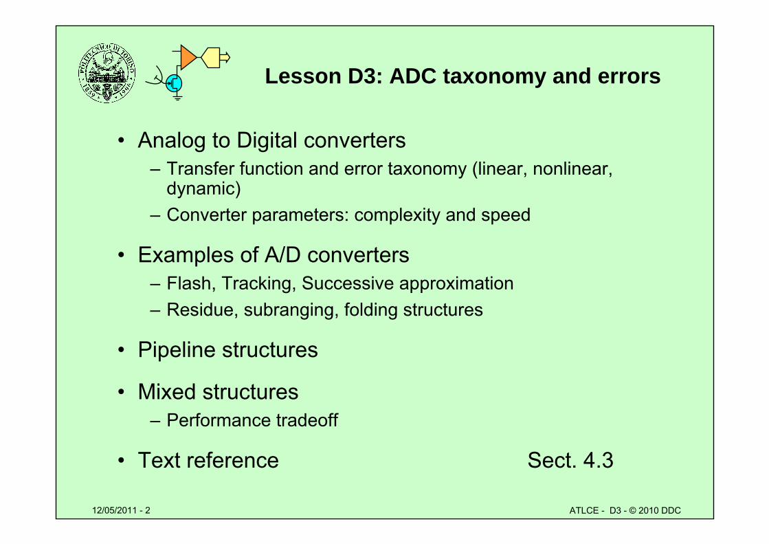
Lesson D3: ADC taxonomy and errors
• Analog to Digital converters– Transfer function and error taxonomy (linear, nonlinear,
dynamic)– Converter parameters: complexity and speed
• Examples of A/D converters– Flash, Tracking, Successive approximation– Residue, subranging, folding structures
• Pipeline structures
• Mixed structures– Performance tradeoff
• Text reference Sect. 4.3
12/05/2011 - 3 ATLCE - D3 - © 2010 DDC
Errors in A/D converters
• Dual transfer function vs D/A– X axis: analog values (continuous)– Y axis: numeric values (discrete)
• Each ADi interval corresponds to a Di value– “stair” transfer function– If N large looks as a continuous line– Same error classification as D/A
» Linear: offset and gain» Nonlinearity: differential and integral» Dynamic parameters
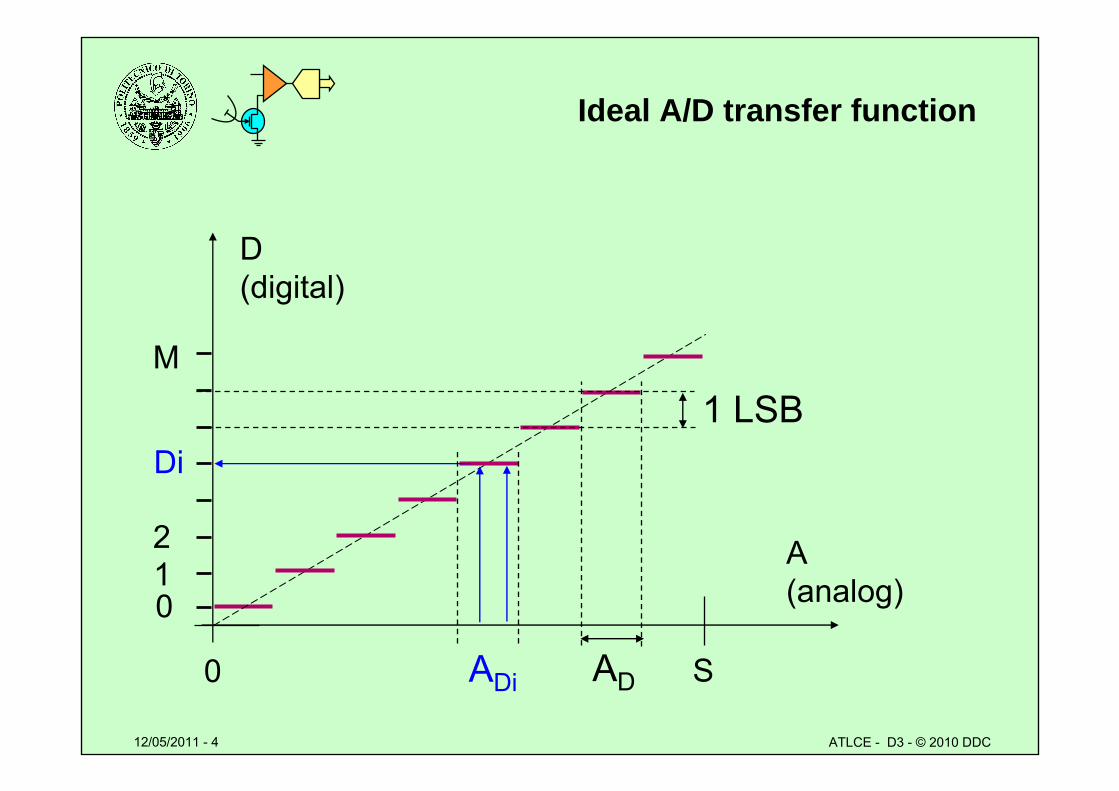
12/05/2011 - 4 ATLCE - D3 - © 2010 DDC
Ideal A/D transfer function
0 S
01
M
2
D(digital)
A(analog)
1 LSB
AD ADi
Di
12/05/2011 - 5 ATLCE - D3 - © 2010 DDC
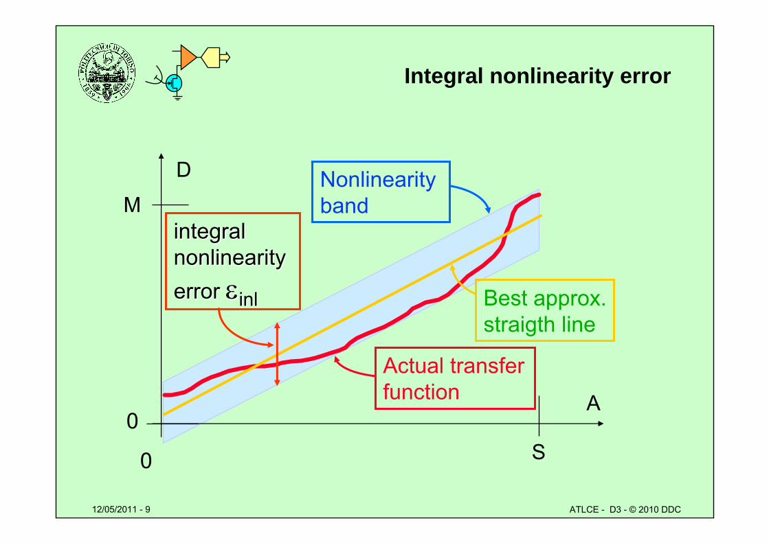
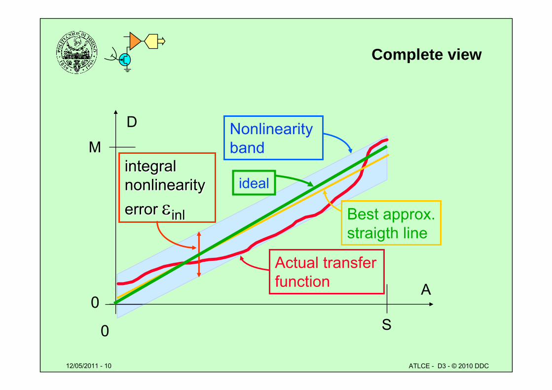
Static errors: two-steps analysis
• Linear approximation of actual transfer function
• Actual transfer function vs linear approximation– Nonlinearity errors: integral nonlinearity
• Linear approximation vs ideal transfer function– Linear errors: offset and gain
• Detailed quantization interval analysis– Differential nonlinearity
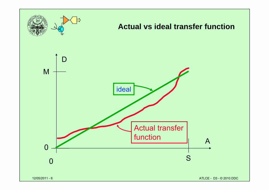
12/05/2011 - 6 ATLCE - D3 - © 2010 DDC
Actual vs ideal transfer function
0
0
Actual transfer function
S
A
M
ideal
D
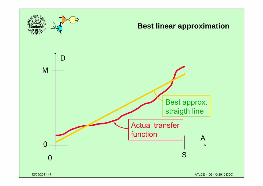
12/05/2011 - 7 ATLCE - D3 - © 2010 DDC
Best linear approximation
0
0
Actual transfer function
Best approx.straigth line
S
D
A
M
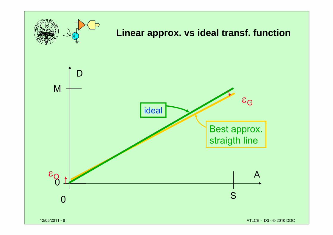
12/05/2011 - 8 ATLCE - D3 - © 2010 DDC
Linear approx. vs ideal transf. function
0
0
Best approx.straigth line
S
D
A
M
idealG
O
12/05/2011 - 9 ATLCE - D3 - © 2010 DDC
Integral nonlinearity error
0
0
Actual transfer function
Nonlinearityband
Best approx.straigth line
integralintegralnonlinearitynonlinearityerror error inlinl
S
D
A
M
12/05/2011 - 10 ATLCE - D3 - © 2010 DDC
Complete view
0
0
Actual transfer function
Nonlinearityband
Best approx.straigth line
integralintegralnonlinearitynonlinearityerror error inlinl
S
D
A
M
ideal
12/05/2011 - 11 ATLCE - D3 - © 2010 DDC
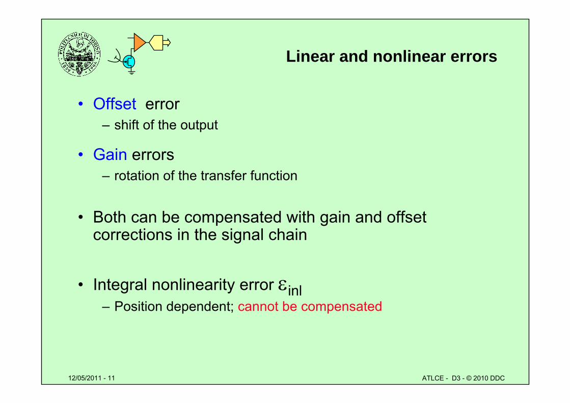
Linear and nonlinear errors
• Offset error– shift of the output
• Gain errors– rotation of the transfer function
• Both can be compensated with gain and offset corrections in the signal chain
• Integral nonlinearity error inl– Position dependent; cannot be compensated
12/05/2011 - 12 ATLCE - D3 - © 2010 DDC
0
AD
0 S
D
A
M
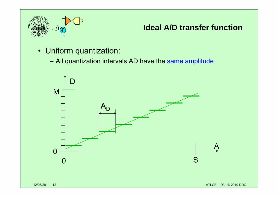
Ideal A/D transfer function
• Uniform quantization:– All quantization intervals AD have the same amplitude
12/05/2011 - 13 ATLCE - D3 - © 2010 DDC
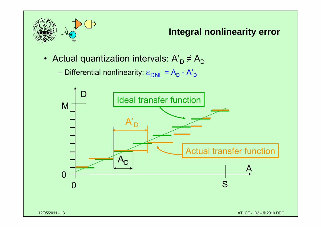
Integral nonlinearity error
• Actual quantization intervals: A’D ≠ AD
– Differential nonlinearity: DNL = AD - A’D
0
A’D
0 S
D
A
M
AD
Actual transfer function
Ideal transfer function
12/05/2011 - 14 ATLCE - D3 - © 2010 DDC
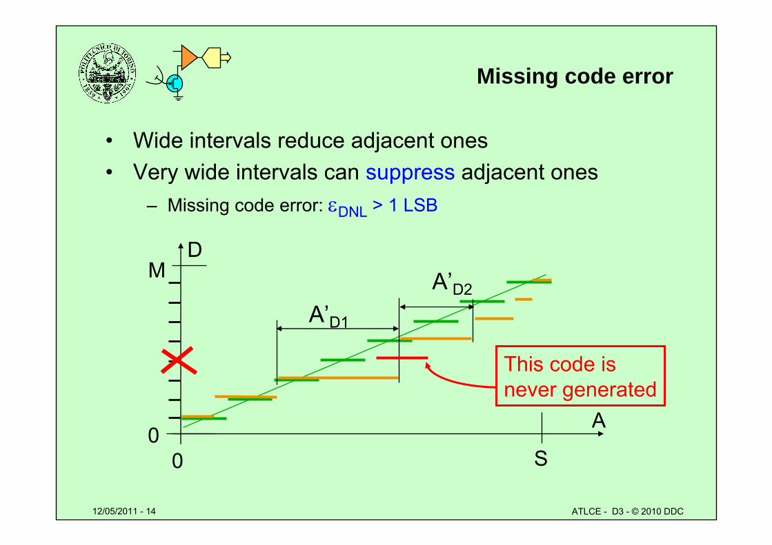
Missing code error
• Wide intervals reduce adjacent ones • Very wide intervals can suppress adjacent ones
– Missing code error: DNL > 1 LSB
00 S
D
A
M
This code isnever generated
A’D1
A’D2
12/05/2011 - 15 ATLCE - D3 - © 2010 DDC
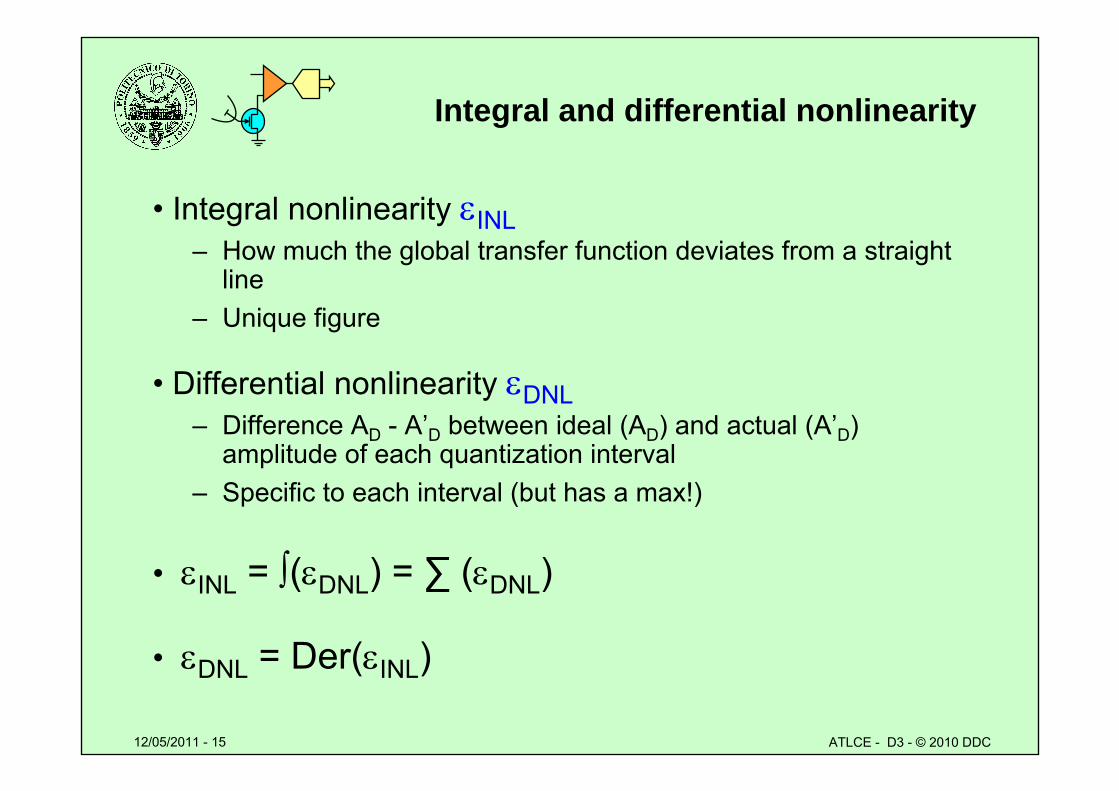
Integral and differential nonlinearity
• Integral nonlinearity INL– How much the global transfer function deviates from a straight
line– Unique figure
• Differential nonlinearity DNL– Difference AD - A’D between ideal (AD) and actual (A’D)
amplitude of each quantization interval– Specific to each interval (but has a max!)
• INL = ∫(DNL) = ∑ (DNL)
• DNL = Der(INL)
12/05/2011 - 16 ATLCE - D3 - © 2010 DDC
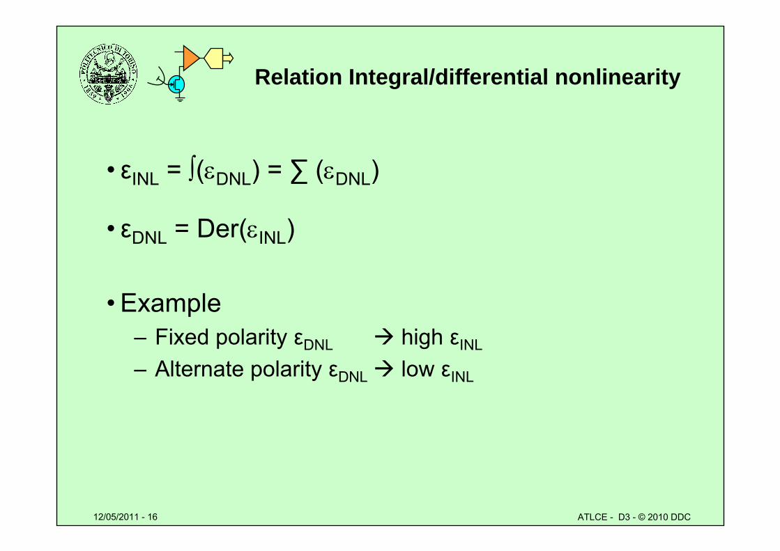
Relation Integral/differential nonlinearity
• εINL = ∫(DNL) = ∑ (DNL)
• εDNL = Der(INL)
• Example – Fixed polarity εDNL high εINL
– Alternate polarity εDNL low εINL
12/05/2011 - 17 ATLCE - D3 - © 2010 DDC
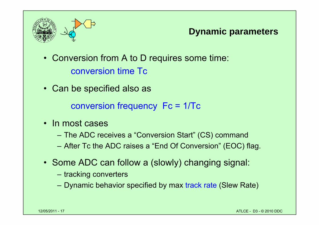
Dynamic parameters
• Conversion from A to D requires some time:conversion time Tc
• Can be specified also as
conversion frequency Fc = 1/Tc
• In most cases – The ADC receives a “Conversion Start” (CS) command – After Tc the ADC raises a “End Of Conversion” (EOC) flag.
• Some ADC can follow a (slowly) changing signal:– tracking converters– Dynamic behavior specified by max track rate (Slew Rate)
12/05/2011 - 18 ATLCE - D3 - © 2010 DDC
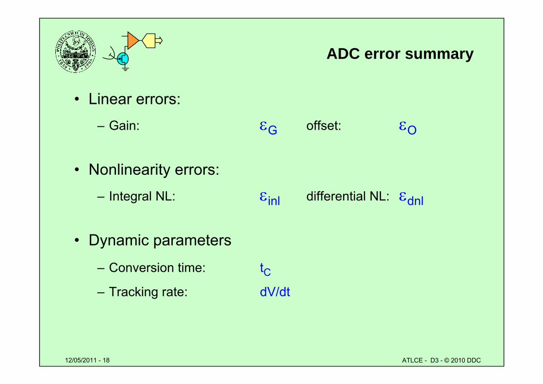
ADC error summary
• Linear errors:– Gain: G offset: O
• Nonlinearity errors:
– Integral NL: inl differential NL: dnl
• Dynamic parameters
– Conversion time: tC– Tracking rate: dV/dt
12/05/2011 - 19 ATLCE - D3 - © 2010 DDC
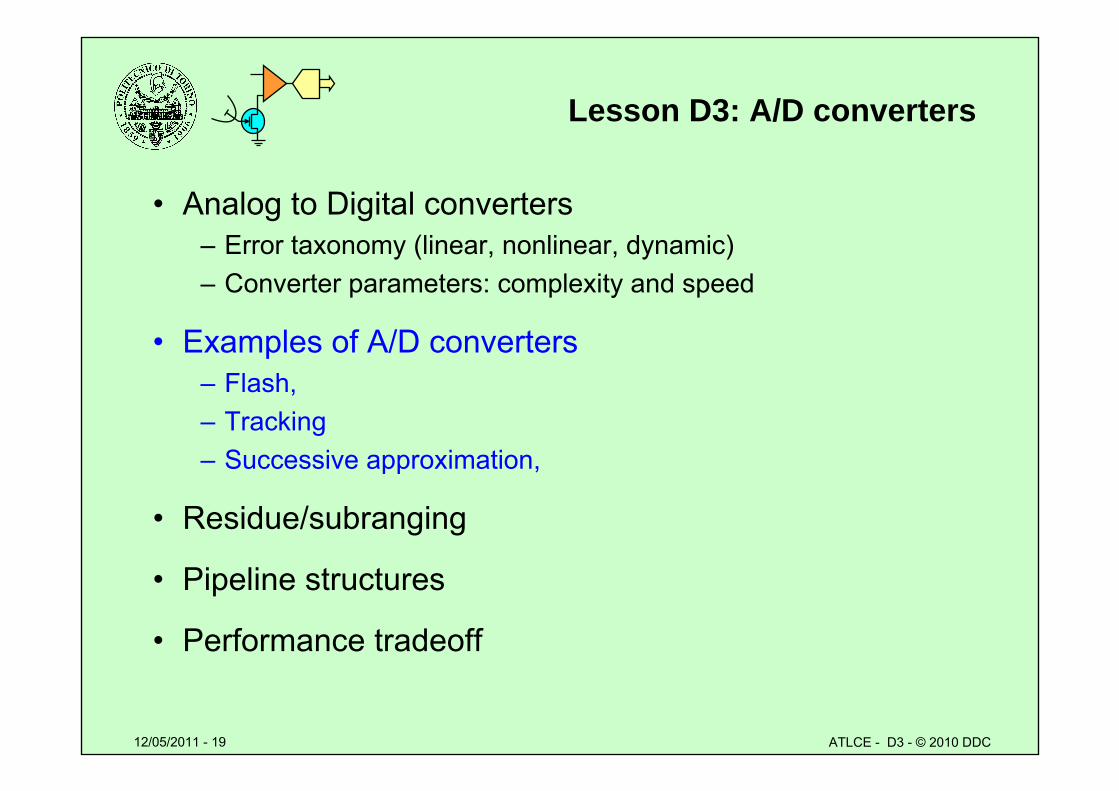
Lesson D3: A/D converters
• Analog to Digital converters– Error taxonomy (linear, nonlinear, dynamic)– Converter parameters: complexity and speed
• Examples of A/D converters– Flash, – Tracking– Successive approximation,
• Residue/subranging
• Pipeline structures
• Performance tradeoff
12/05/2011 - 20 ATLCE - D3 - © 2010 DDC
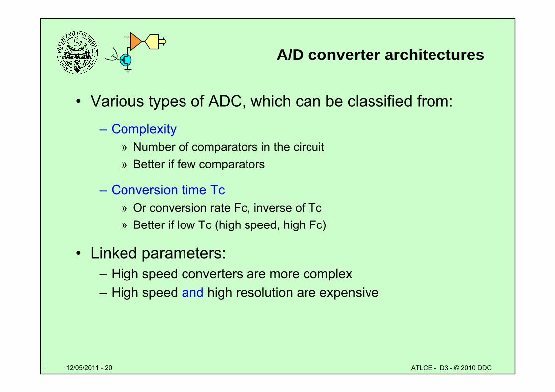
A/D converter architectures
• Various types of ADC, which can be classified from:
– Complexity» Number of comparators in the circuit» Better if few comparators
– Conversion time Tc» Or conversion rate Fc, inverse of Tc» Better if low Tc (high speed, high Fc)
• Linked parameters:– High speed converters are more complex– High speed and high resolution are expensive
.
12/05/2011 - 21 ATLCE - D3 - © 2010 DDC
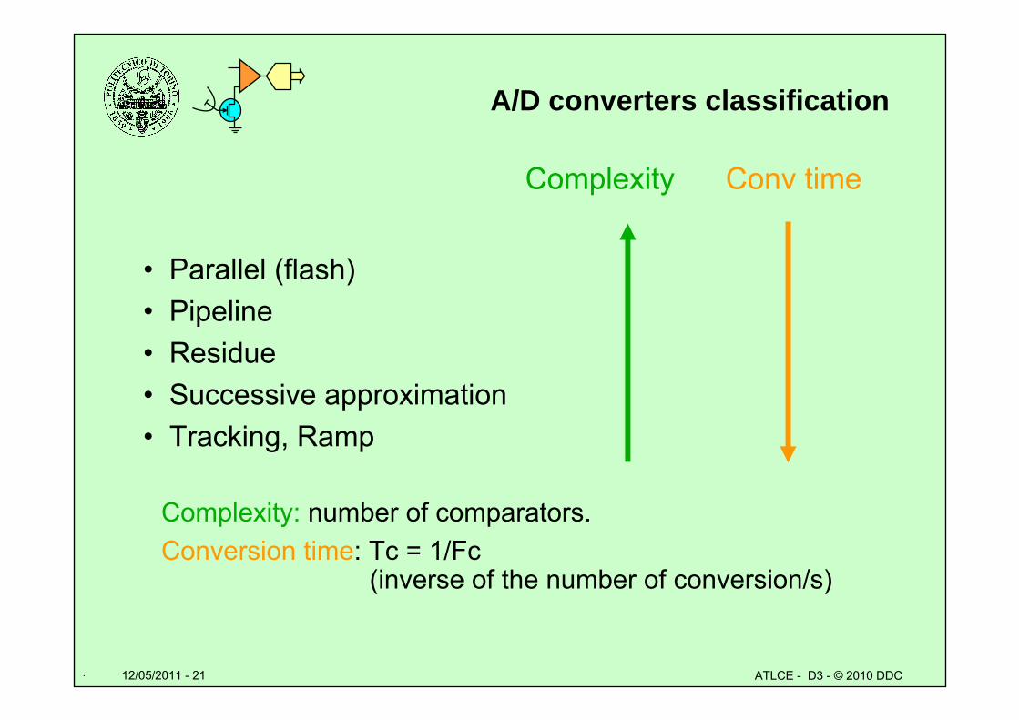
A/D converters classification
• Parallel (flash)• Pipeline• Residue• Successive approximation • Tracking, Ramp
Complexity: number of comparators.Conversion time: Tc = 1/Fc
(inverse of the number of conversion/s)
.
Complexity Conv time
12/05/2011 - 22 ATLCE - D3 - © 2010 DDC
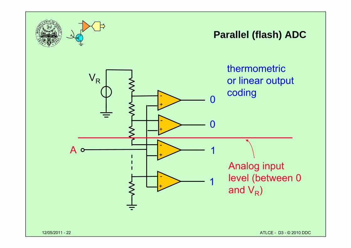
Parallel (flash) ADC
VR
-+
-+
-+
-+
A
thermometricor linear output coding
0
1
1
0
Analog input level (between 0 and VR)
12/05/2011 - 23 ATLCE - D3 - © 2010 DDC
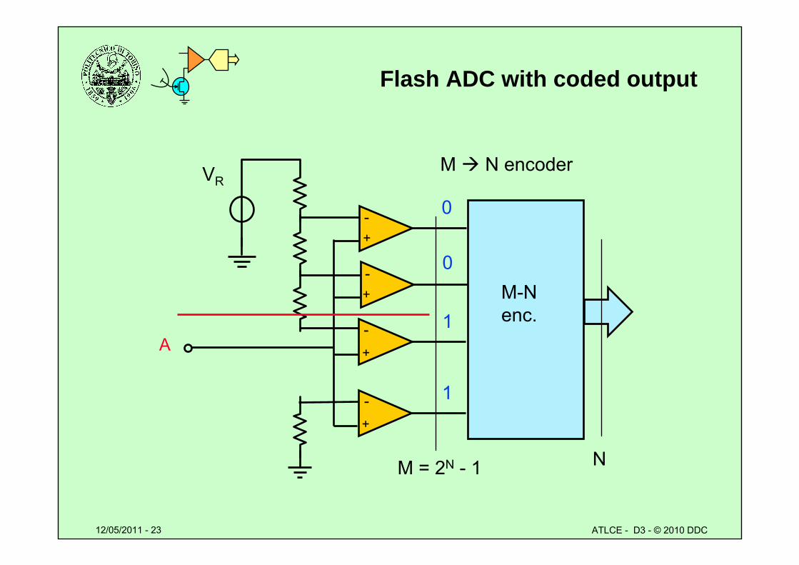
Flash ADC with coded output
VR
-+
-+
-+
-+
A
0
1
1
0
M N encoder
M = 2N - 1 N
M-Nenc.
12/05/2011 - 24 ATLCE - D3 - © 2010 DDC
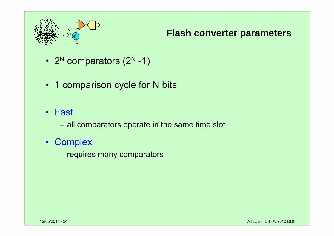
Flash converter parameters
• 2N comparators (2N -1)
• 1 comparison cycle for N bits
• Fast– all comparators operate in the same time slot
• Complex – requires many comparators
12/05/2011 - 25 ATLCE - D3 - © 2010 DDC
Logic network-+A
D
A’
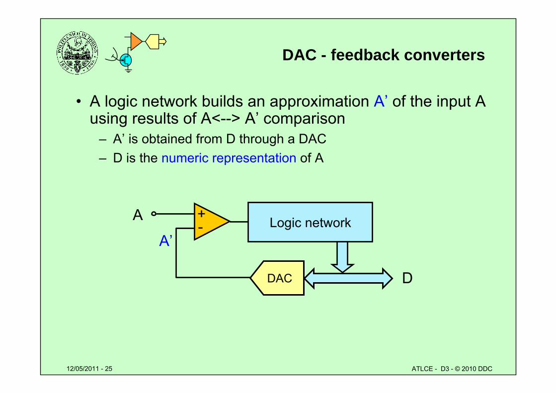
DAC - feedback converters
• A logic network builds an approximation A’ of the input A using results of A<--> A’ comparison
– A’ is obtained from D through a DAC– D is the numeric representation of A
DAC
12/05/2011 - 26 ATLCE - D3 - © 2010 DDC
Feedback converters algorithms
• The logic network modifies D till A’ becomes the best approximation of A (within the N-bit resolution)
• Two procedures:
• Steps of one LSB:– tracking converters– 2N steps for full scale change; conversion time: TC = 2N TCK
• Start from MSB:– successive approximation converters– N steps for any conversion: TC = N TCK
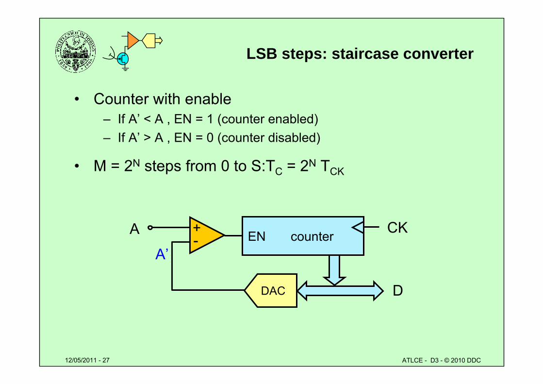
12/05/2011 - 27 ATLCE - D3 - © 2010 DDC
LSB steps: staircase converter
• Counter with enable– If A’ < A , EN = 1 (counter enabled)– If A’ > A , EN = 0 (counter disabled)
• M = 2N steps from 0 to S:TC = 2N TCK
EN counter-+A
D
A’
DAC
CK
12/05/2011 - 28 ATLCE - D3 - © 2010 DDC
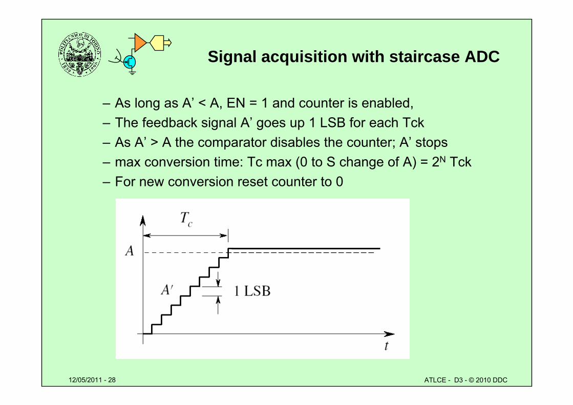
Signal acquisition with staircase ADC
– As long as A’ < A, EN = 1 and counter is enabled, – The feedback signal A’ goes up 1 LSB for each Tck– As A’ > A the comparator disables the counter; A’ stops– max conversion time: Tc max (0 to S change of A) = 2N Tck– For new conversion reset counter to 0
12/05/2011 - 29 ATLCE - D3 - © 2010 DDC
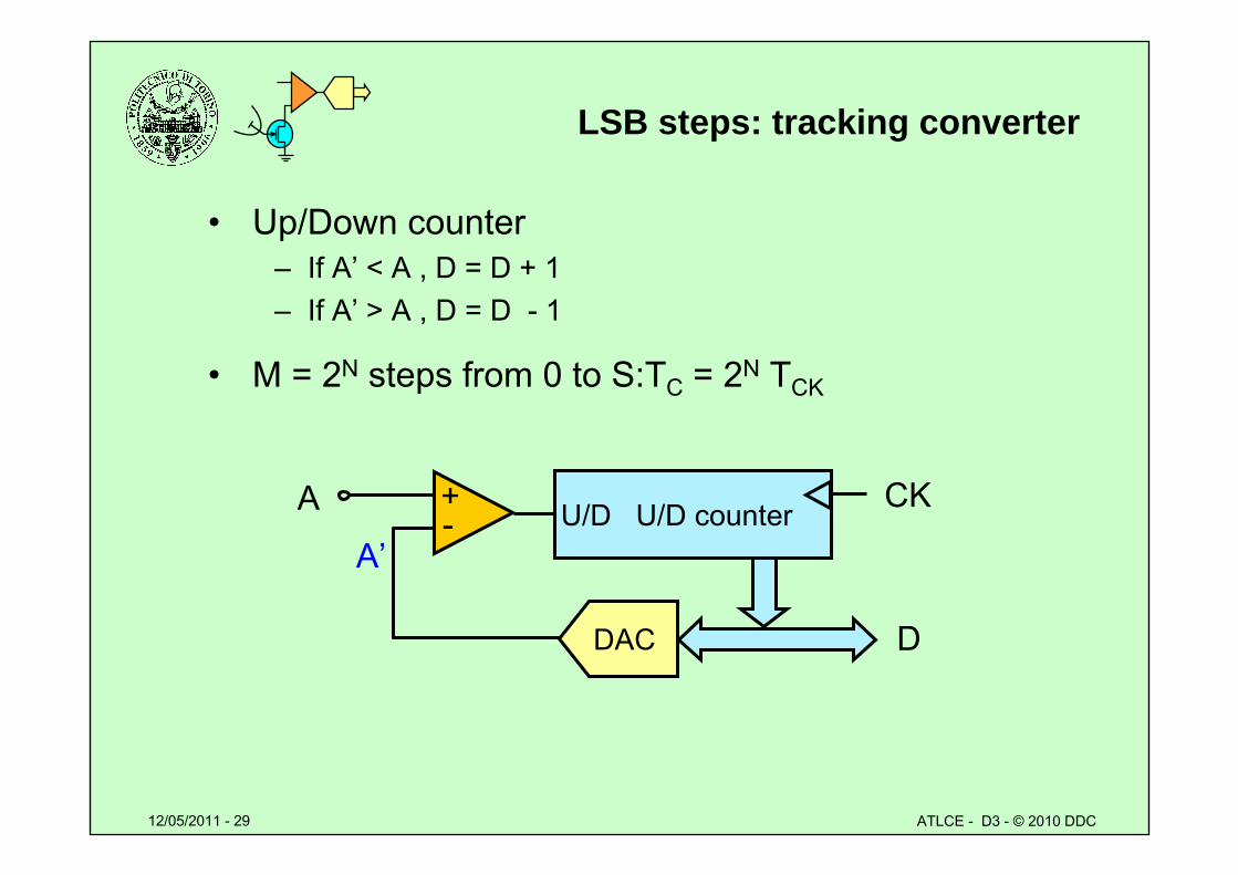
LSB steps: tracking converter
• Up/Down counter– If A’ < A , D = D + 1– If A’ > A , D = D - 1
• M = 2N steps from 0 to S:TC = 2N TCK
U/D U/D counter-+A
D
A’
DAC
CK
12/05/2011 - 30 ATLCE - D3 - © 2010 DDC
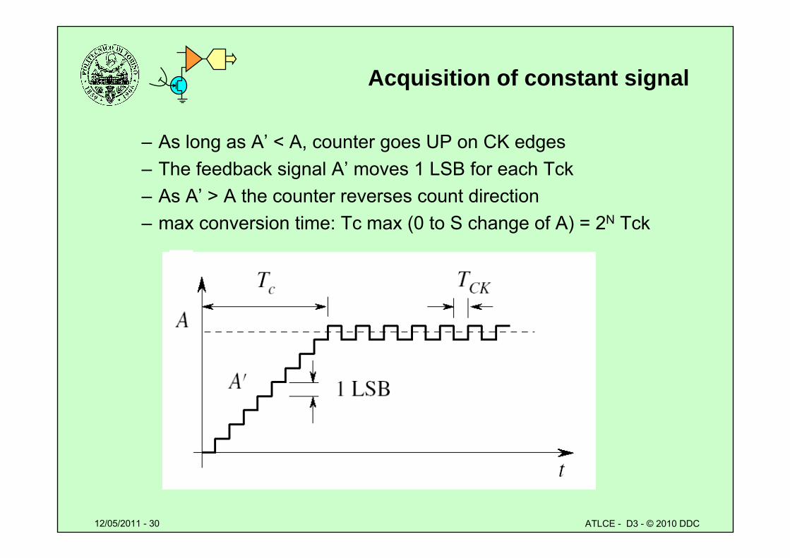
Acquisition of constant signal
– As long as A’ < A, counter goes UP on CK edges– The feedback signal A’ moves 1 LSB for each Tck– As A’ > A the counter reverses count direction– max conversion time: Tc max (0 to S change of A) = 2N Tck
12/05/2011 - 31 ATLCE - D3 - © 2010 DDC
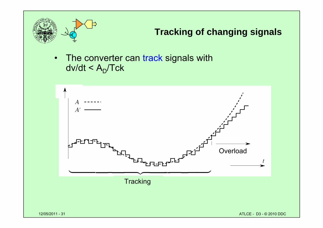
Tracking of changing signals
• The converter can track signals with dv/dt < AD/Tck
Tracking
Overload
12/05/2011 - 32 ATLCE - D3 - © 2010 DDC
Tracking converter parameters
• 1 comparator
• 2N comparison cycle for N bits
• Slow – fully sequential decisions– limited dV/dt tracking capability
• Simple – requires a single comparator
12/05/2011 - 33 ATLCE - D3 - © 2010 DDC
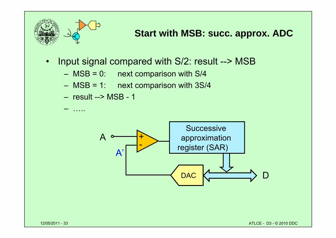
Start with MSB: succ. approx. ADC
• Input signal compared with S/2: result --> MSB– MSB = 0: next comparison with S/4– MSB = 1: next comparison with 3S/4– result --> MSB - 1– …..
Successive approximation
register (SAR) -+A
D
A’
DAC
12/05/2011 - 34 ATLCE - D3 - © 2010 DDC
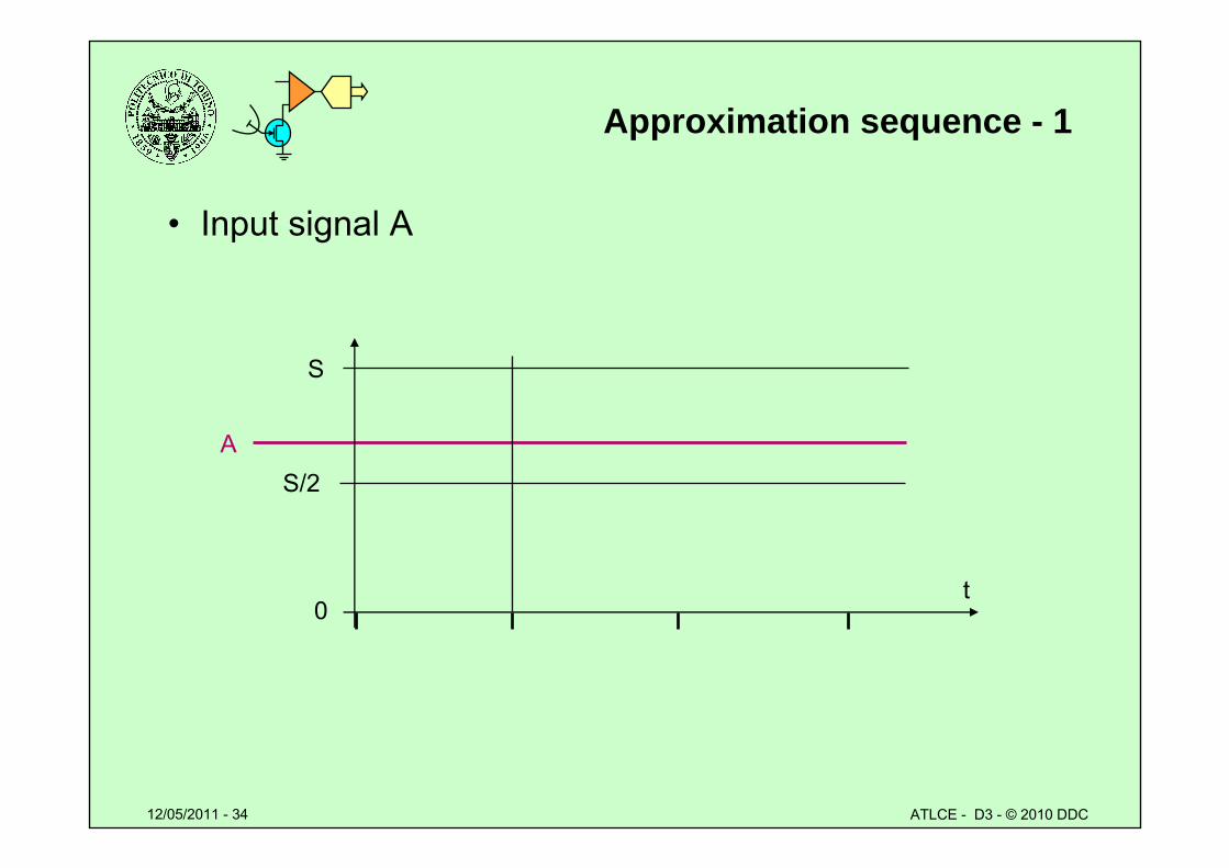
Approximation sequence - 1
• Input signal A
S
0
S/2A
t
12/05/2011 - 35 ATLCE - D3 - © 2010 DDC
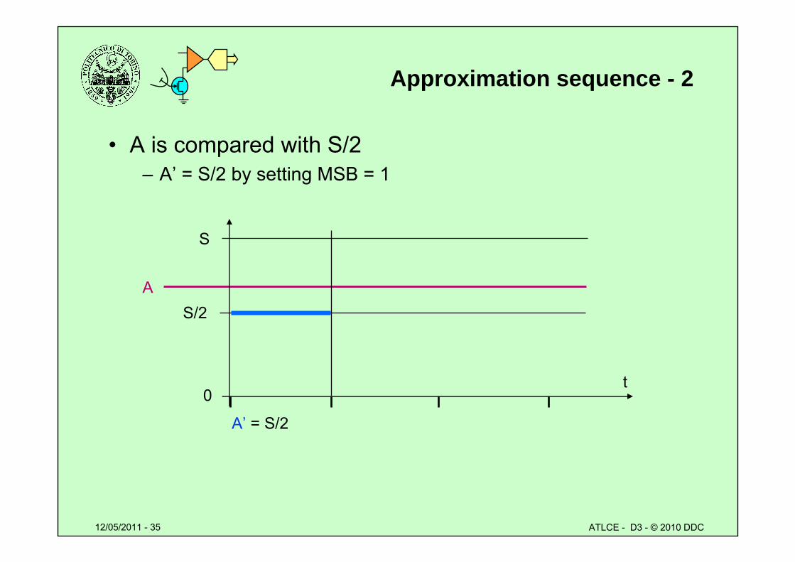
Approximation sequence - 2
• A is compared with S/2 – A’ = S/2 by setting MSB = 1
S
0
S/2
A’ = S/2
A
t
12/05/2011 - 36 ATLCE - D3 - © 2010 DDC
Approximation sequence - 3
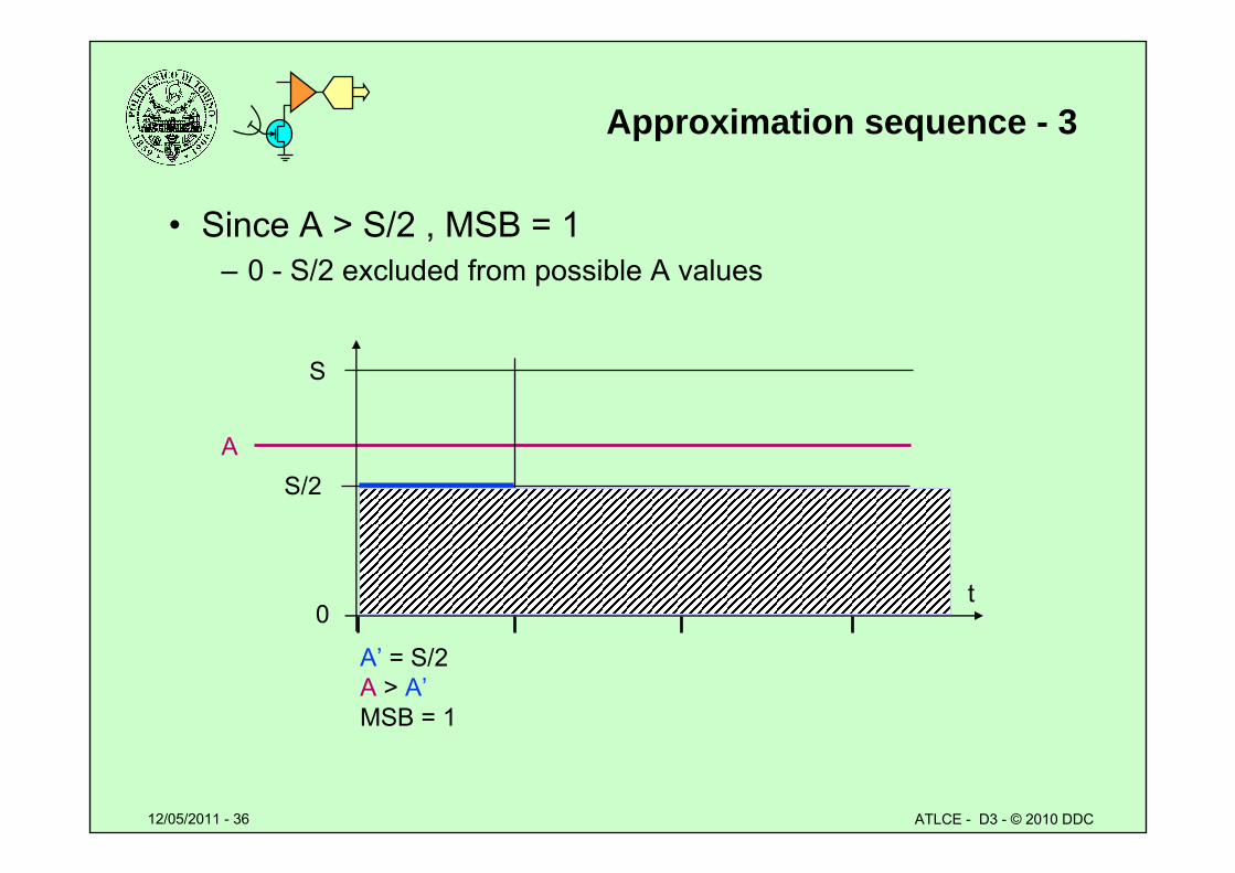
• Since A > S/2 , MSB = 1– 0 - S/2 excluded from possible A values
S
0
S/2
A’ = S/2A > A’MSB = 1
A
t
12/05/2011 - 37 ATLCE - D3 - © 2010 DDC
Approximation sequence - 4
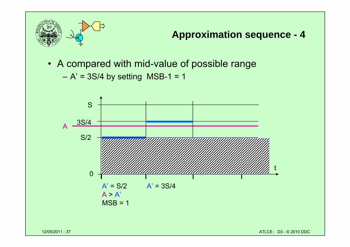
• A compared with mid-value of possible range– A’ = 3S/4 by setting MSB-1 = 1
S
0
S/2
3S/4
A’ = S/2A > A’MSB = 1
A
t
A’ = 3S/4
12/05/2011 - 38 ATLCE - D3 - © 2010 DDC
Approximation sequence - 5
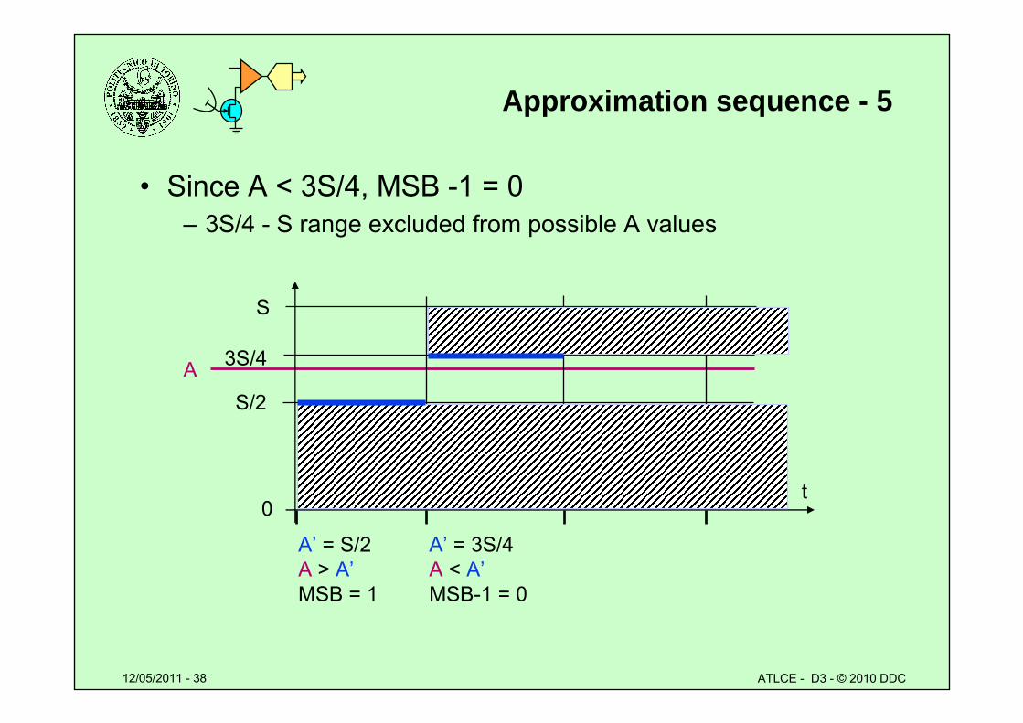
• Since A < 3S/4, MSB -1 = 0– 3S/4 - S range excluded from possible A values
S
0
S/2
3S/4
A’ = S/2A > A’MSB = 1
A
A’ = 3S/4A < A’MSB-1 = 0
t
12/05/2011 - 39 ATLCE - D3 - © 2010 DDC
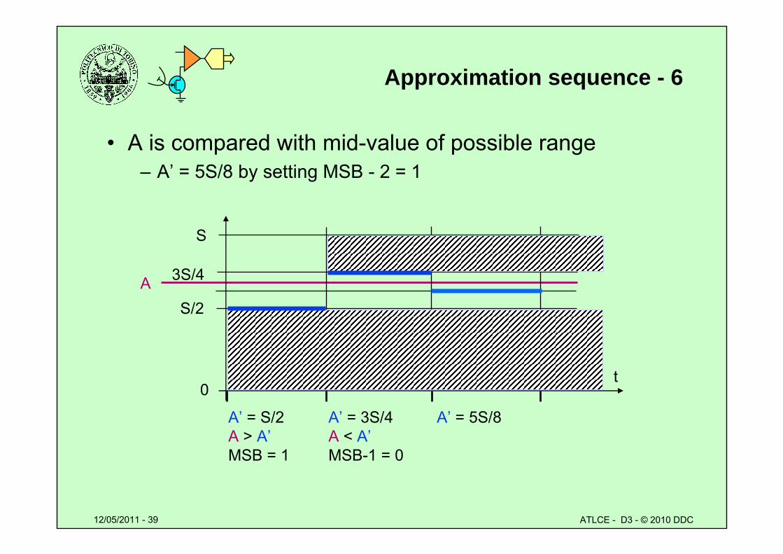
Approximation sequence - 6
• A is compared with mid-value of possible range– A’ = 5S/8 by setting MSB - 2 = 1
S
0
S/2
3S/4
A’ = S/2A > A’MSB = 1
A
A’ = 3S/4A < A’MSB-1 = 0
t
A’ = 5S/8
12/05/2011 - 40 ATLCE - D3 - © 2010 DDC
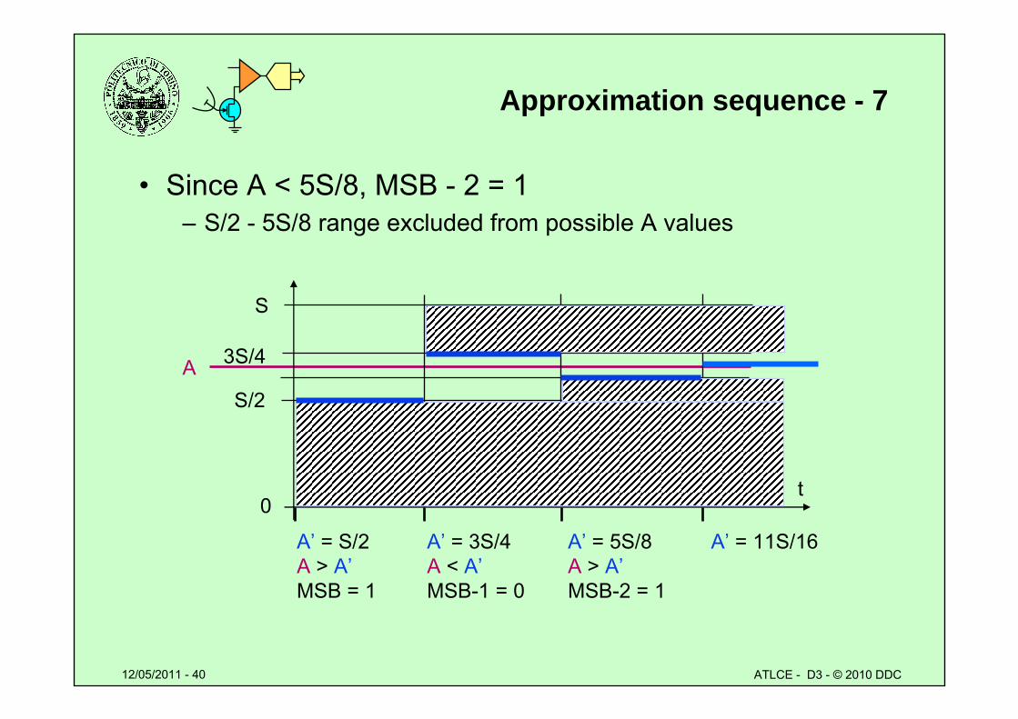
Approximation sequence - 7
• Since A < 5S/8, MSB - 2 = 1– S/2 - 5S/8 range excluded from possible A values
S
0
S/2
3S/4
A’ = S/2A > A’MSB = 1
A
A’ = 3S/4A < A’MSB-1 = 0
t
A’ = 5S/8A > A’MSB-2 = 1
A’ = 11S/16
12/05/2011 - 41 ATLCE - D3 - © 2010 DDC
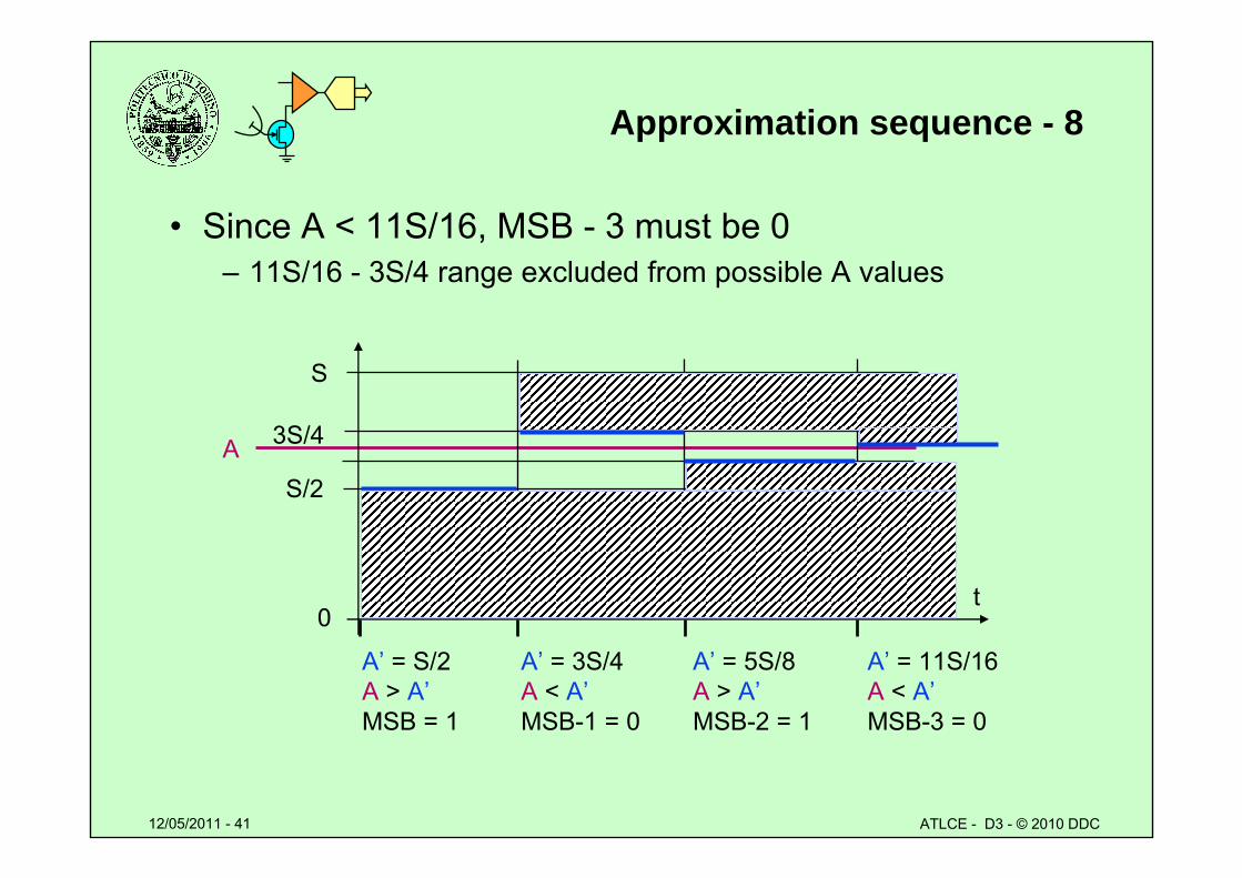
Approximation sequence - 8
• Since A < 11S/16, MSB - 3 must be 0– 11S/16 - 3S/4 range excluded from possible A values
S
0
S/2
3S/4
A’ = S/2A > A’MSB = 1
A
A’ = 3S/4A < A’MSB-1 = 0
t
A’ = 5S/8A > A’MSB-2 = 1
A’ = 11S/16A < A’MSB-3 = 0
12/05/2011 - 42 ATLCE - D3 - © 2010 DDC
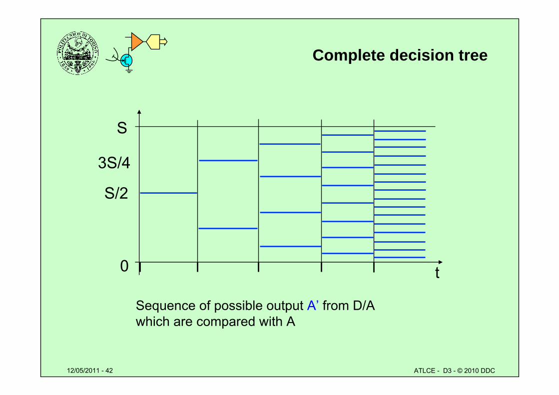
Complete decision tree
S
0
S/2
3S/4
Sequence of possible output A’ from D/A which are compared with A
t
12/05/2011 - 43 ATLCE - D3 - © 2010 DDC
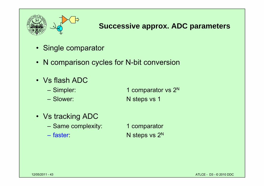
Successive approx. ADC parameters
• Single comparator
• N comparison cycles for N-bit conversion
• Vs flash ADC– Simpler: 1 comparator vs 2N
– Slower: N steps vs 1
• Vs tracking ADC– Same complexity: 1 comparator– faster: N steps vs 2N
12/05/2011 - 44 ATLCE - D3 - © 2010 DDC
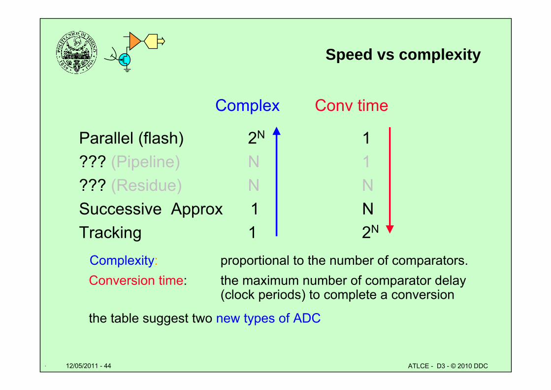
Speed vs complexity
Complex Conv time
Parallel (flash) 2N 1??? (Pipeline) N 1??? (Residue) N NSuccessive Approx 1 NTracking 1 2N
Complexity: proportional to the number of comparators.Conversion time: the maximum number of comparator delay
(clock periods) to complete a conversion
the table suggest two new types of ADC
.
12/05/2011 - 45 ATLCE - D3 - © 2010 DDC
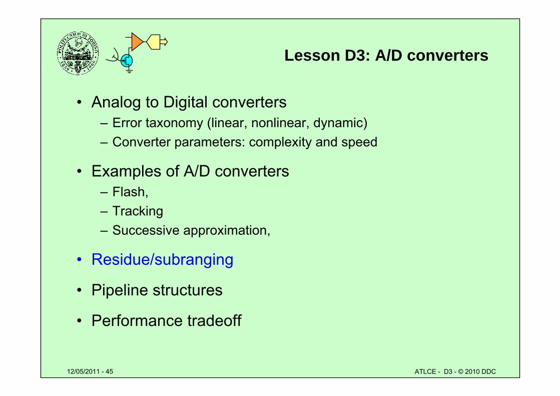
Lesson D3: A/D converters
• Analog to Digital converters– Error taxonomy (linear, nonlinear, dynamic)– Converter parameters: complexity and speed
• Examples of A/D converters– Flash, – Tracking– Successive approximation,
• Residue/subranging
• Pipeline structures
• Performance tradeoff
12/05/2011 - 46 ATLCE - D3 - © 2010 DDC
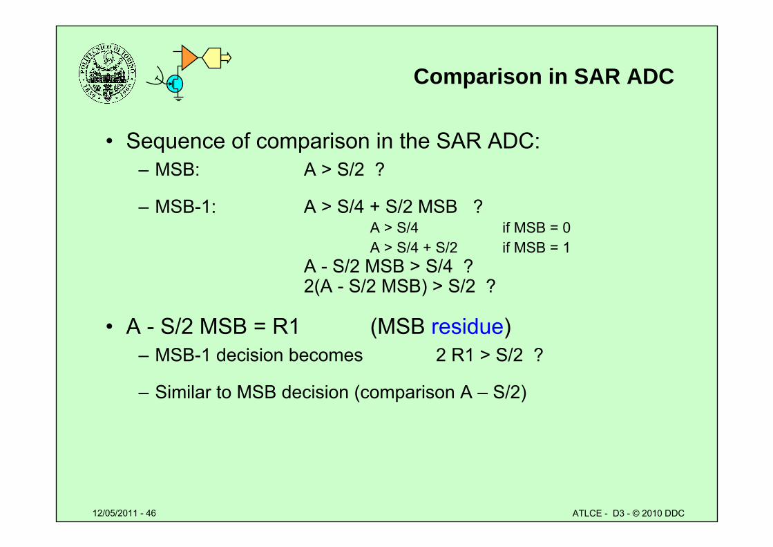
Comparison in SAR ADC
• Sequence of comparison in the SAR ADC:– MSB: A > S/2 ?
– MSB-1: A > S/4 + S/2 MSB ?A > S/4 if MSB = 0A > S/4 + S/2 if MSB = 1
A - S/2 MSB > S/4 ?2(A - S/2 MSB) > S/2 ?
• A - S/2 MSB = R1 (MSB residue)– MSB-1 decision becomes 2 R1 > S/2 ?
– Similar to MSB decision (comparison A – S/2)
12/05/2011 - 47 ATLCE - D3 - © 2010 DDC
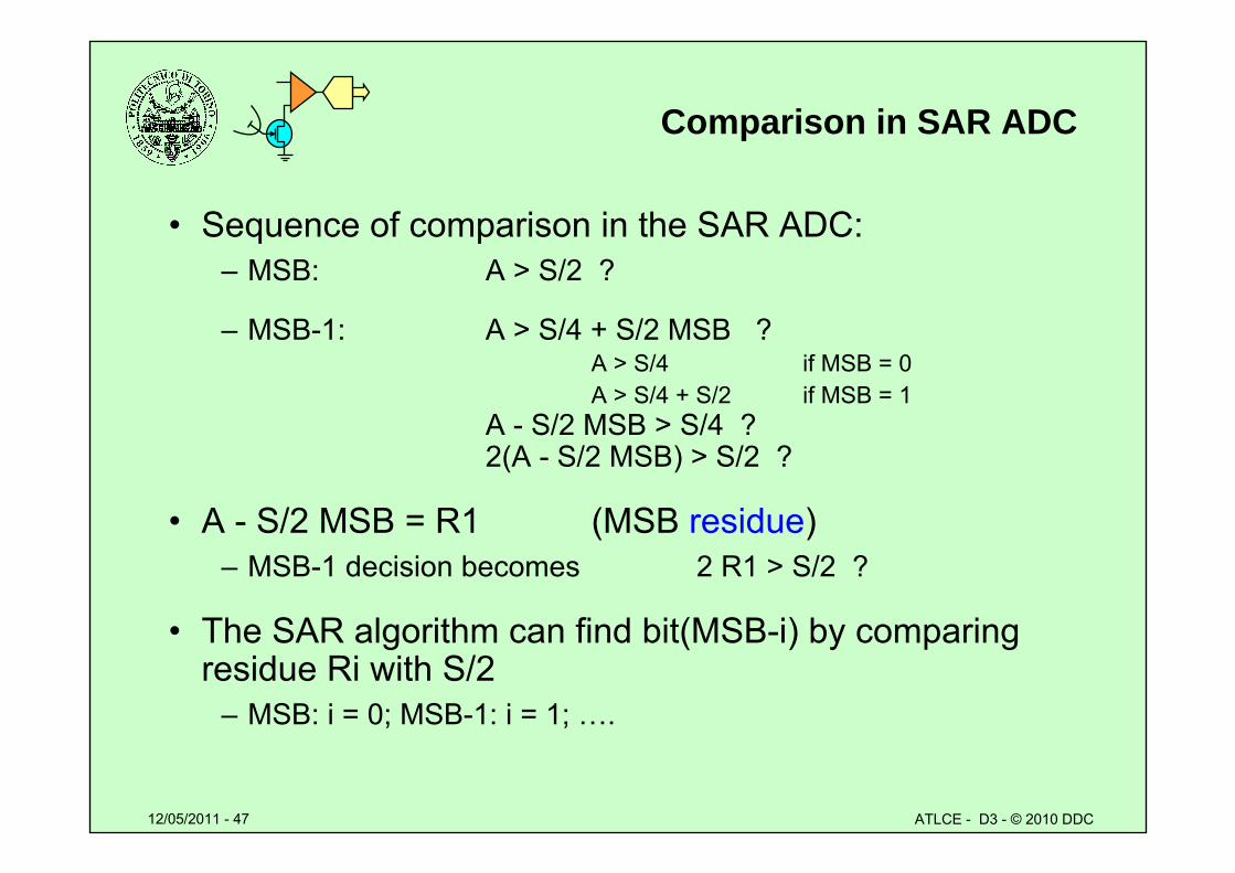
Comparison in SAR ADC
• Sequence of comparison in the SAR ADC:– MSB: A > S/2 ?
– MSB-1: A > S/4 + S/2 MSB ?A > S/4 if MSB = 0A > S/4 + S/2 if MSB = 1
A - S/2 MSB > S/4 ?2(A - S/2 MSB) > S/2 ?
• A - S/2 MSB = R1 (MSB residue)– MSB-1 decision becomes 2 R1 > S/2 ?
• The SAR algorithm can find bit(MSB-i) by comparing residue Ri with S/2
– MSB: i = 0; MSB-1: i = 1; ….
12/05/2011 - 48 ATLCE - D3 - © 2010 DDC
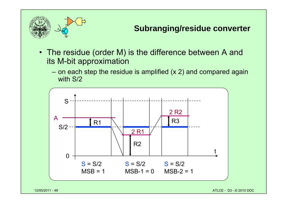
Subranging/residue converter
• The residue (order M) is the difference between A and its M-bit approximation
– on each step the residue is amplified (x 2) and compared again with S/2
S
0
S/2
S = S/2MSB = 1
A
t
R1
S = S/2MSB-1 = 0
2 R1
R2
2 R2 R3
S = S/2MSB-2 = 1
12/05/2011 - 49 ATLCE - D3 - © 2010 DDC
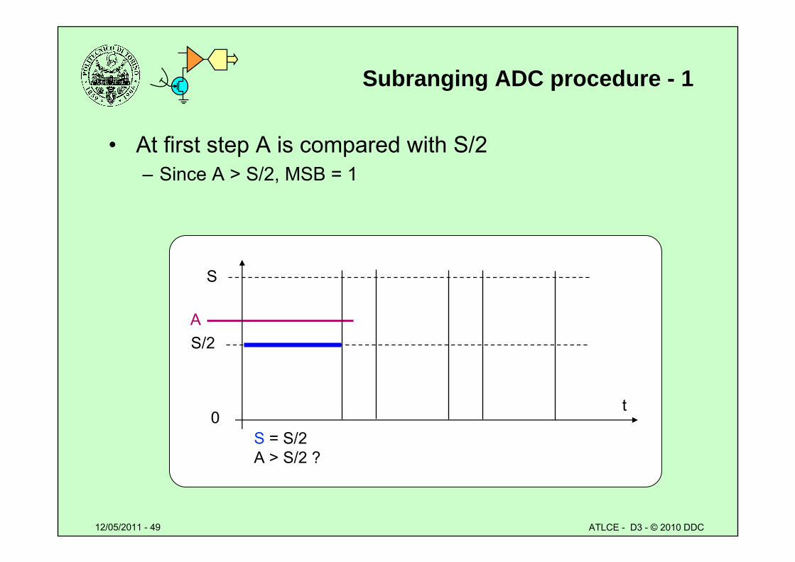
Subranging ADC procedure - 1
• At first step A is compared with S/2– Since A > S/2, MSB = 1
S
0
S/2
S = S/2A > S/2 ?
A
t
12/05/2011 - 50 ATLCE - D3 - © 2010 DDC
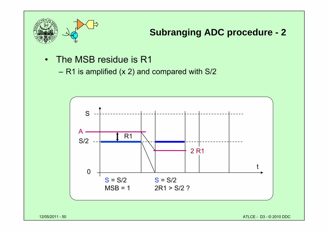
Subranging ADC procedure - 2
• The MSB residue is R1– R1 is amplified (x 2) and compared with S/2
S
0
S/2
S = S/2MSB = 1
A
t
R1
S = S/22R1 > S/2 ?
2 R1
12/05/2011 - 51 ATLCE - D3 - © 2010 DDC
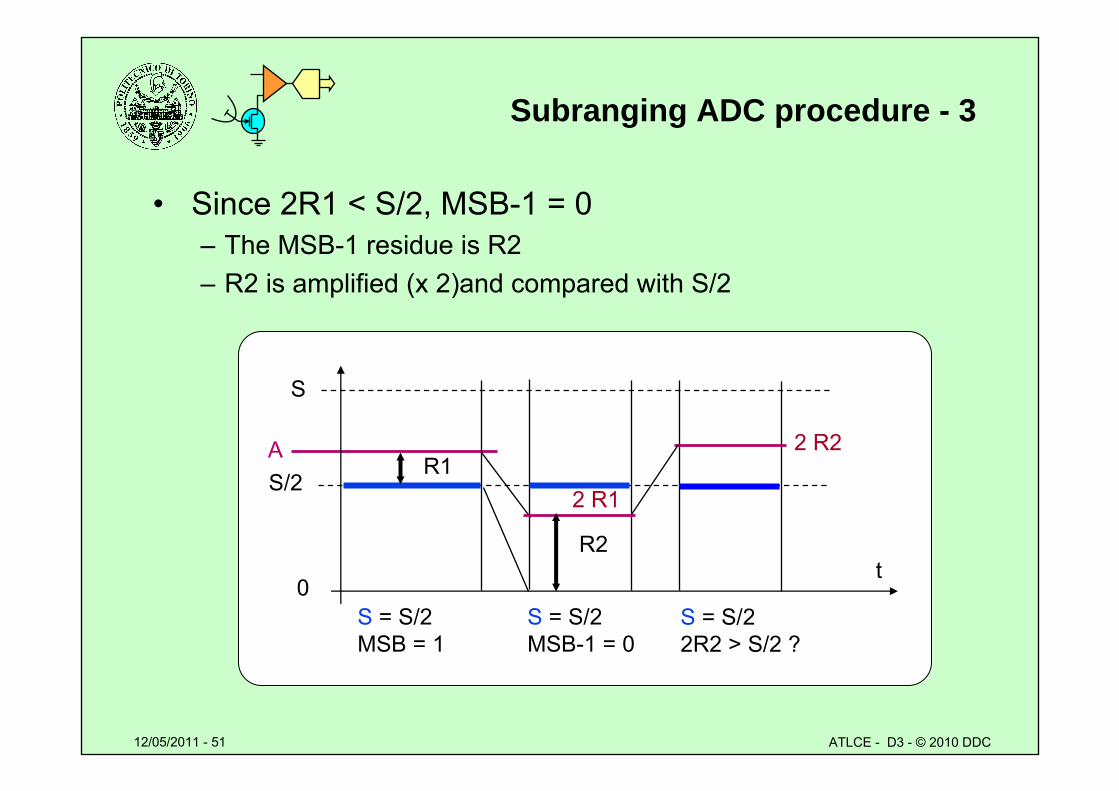
Subranging ADC procedure - 3
• Since 2R1 < S/2, MSB-1 = 0– The MSB-1 residue is R2– R2 is amplified (x 2)and compared with S/2
S
0
S/2
S = S/2MSB = 1
A
t
R1
S = S/2MSB-1 = 0
2 R1
R2
2 R2
S = S/22R2 > S/2 ?
12/05/2011 - 52 ATLCE - D3 - © 2010 DDC
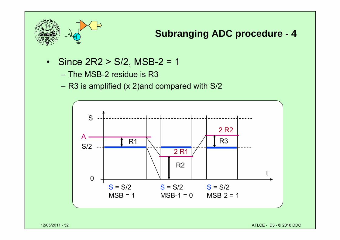
Subranging ADC procedure - 4
• Since 2R2 > S/2, MSB-2 = 1– The MSB-2 residue is R3– R3 is amplified (x 2)and compared with S/2
S
0
S/2
S = S/2MSB = 1
A
t
R1
S = S/2MSB-1 = 0
2 R1
R2
2 R2 R3
S = S/2MSB-2 = 1
12/05/2011 - 53 ATLCE - D3 - © 2010 DDC
Subranging ADC procedure - 5
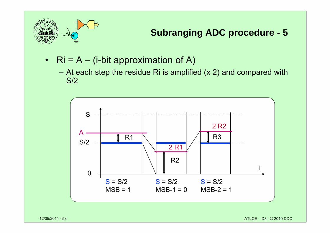
• Ri = A – (i-bit approximation of A)– At each step the residue Ri is amplified (x 2) and compared with
S/2
S
0
S/2
S = S/2MSB = 1
A
t
R1
S = S/2MSB-1 = 0
2 R1
R2
2 R2
S = S/2MSB-2 = 1
R3
12/05/2011 - 54 ATLCE - D3 - © 2010 DDC
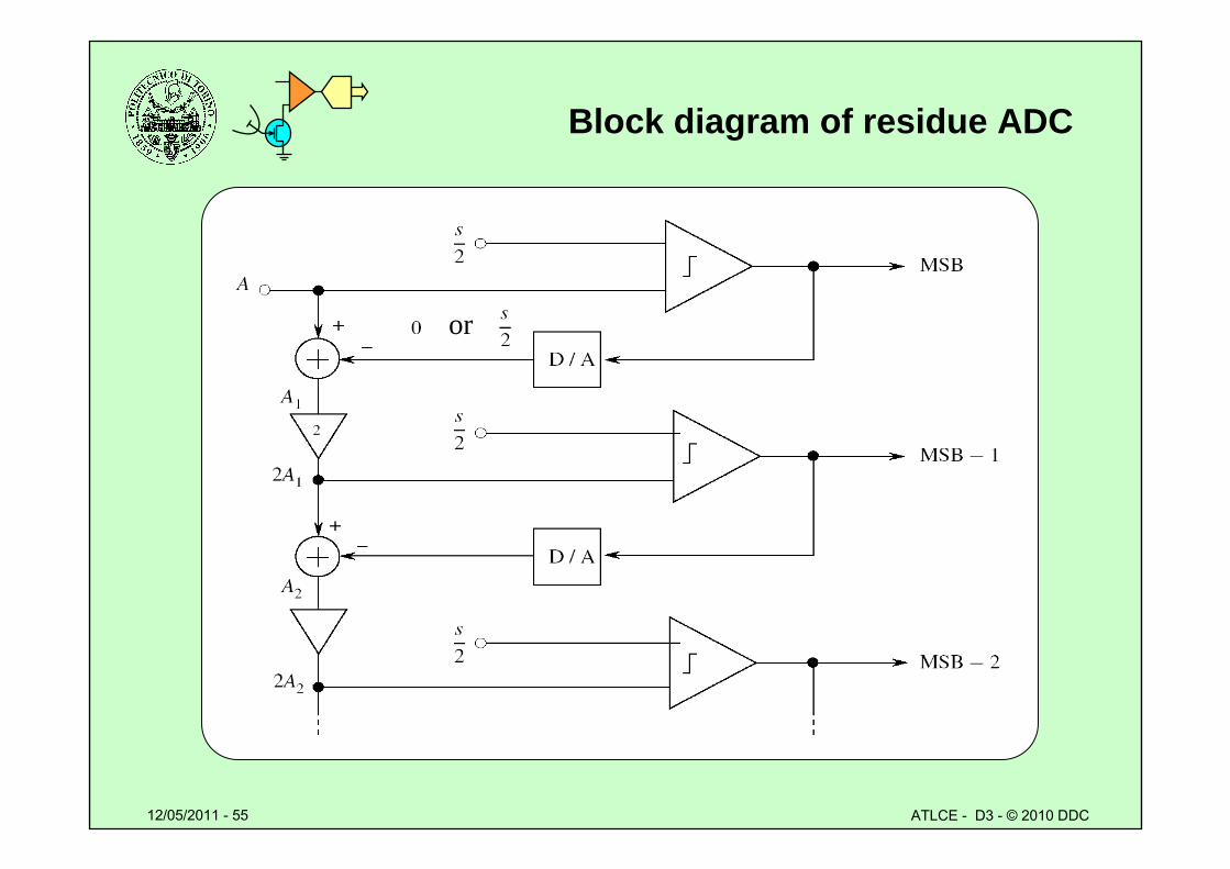
Residue converter parameters
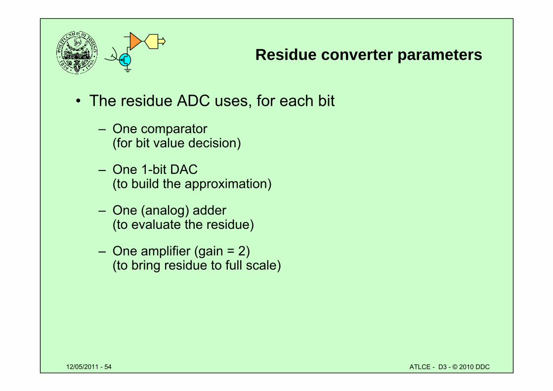
• The residue ADC uses, for each bit
– One comparator (for bit value decision)
– One 1-bit DAC(to build the approximation)
– One (analog) adder (to evaluate the residue)
– One amplifier (gain = 2) (to bring residue to full scale)
12/05/2011 - 55 ATLCE - D3 - © 2010 DDC
Block diagram of residue ADC
or
12/05/2011 - 56 ATLCE - D3 - © 2010 DDC
Precision in subranging converters
• Any error in residue evaluation is propagated to the following stages
– residue must be evaluated with a resolution corresponding to the residual bit number
» ADC precision» DAC precision» Amplifiers and S/H (pipeline) precision
• Previous example– First stage ADC and DAC (1-bit) need 8-bit precision– precision decreases towards LSBs
12/05/2011 - 57 ATLCE - D3 - © 2010 DDC
Subranging ADC parameters
• N comparators
• N comparison cycles for N-bit conversion
• Vs successive approximation ADC– Higher complexity: N vs 1 comparator– Same speed: N steps
• No benefit
• Useful as starting structure for pipeline ADC
12/05/2011 - 58 ATLCE - D3 - © 2010 DDC
Lesson D3: A/D converters
• Analog to Digital converters– Error taxonomy (linear, nonlinear, dynamic)– Converter parameters: complexity and speed
• Examples of A/D converters– Flash, – Tracking– Successive approximation,
• Residue/subranging
• Pipeline structures
• Performance tradeoff
12/05/2011 - 59 ATLCE - D3 - © 2010 DDC
Multistage pipeline converters
• Operate on different samples at the same time– Input sample 1– Input sample 2, processA 1– Input sample 3, processA 2, processB 1– ….– …. ProcessZ 1– …. Output sample 1
• Needs analog memory elements
12/05/2011 - 60 ATLCE - D3 - © 2010 DDC
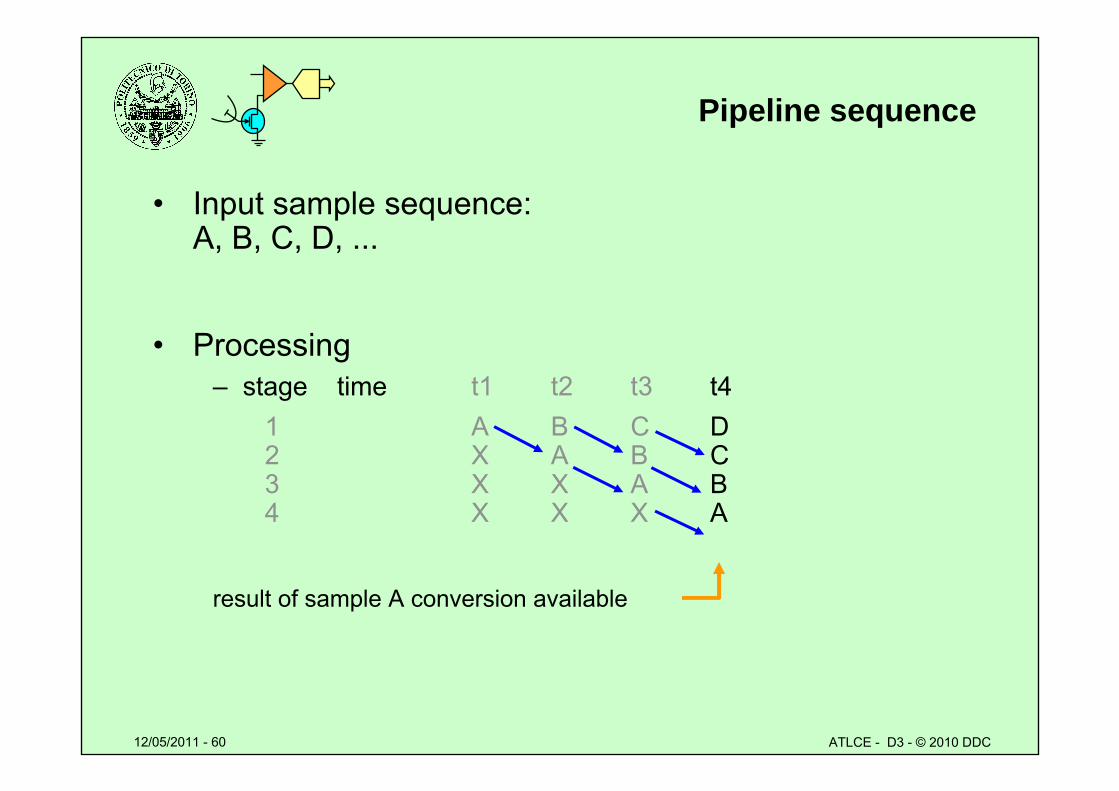
Pipeline sequence
• Input sample sequence:A, B, C, D, ...
• Processing – stage time t1 t2 t3 t4
1 A B C D2 X A B C3 X X A B4 X X X A
result of sample A conversion available
12/05/2011 - 61 ATLCE - D3 - © 2010 DDC
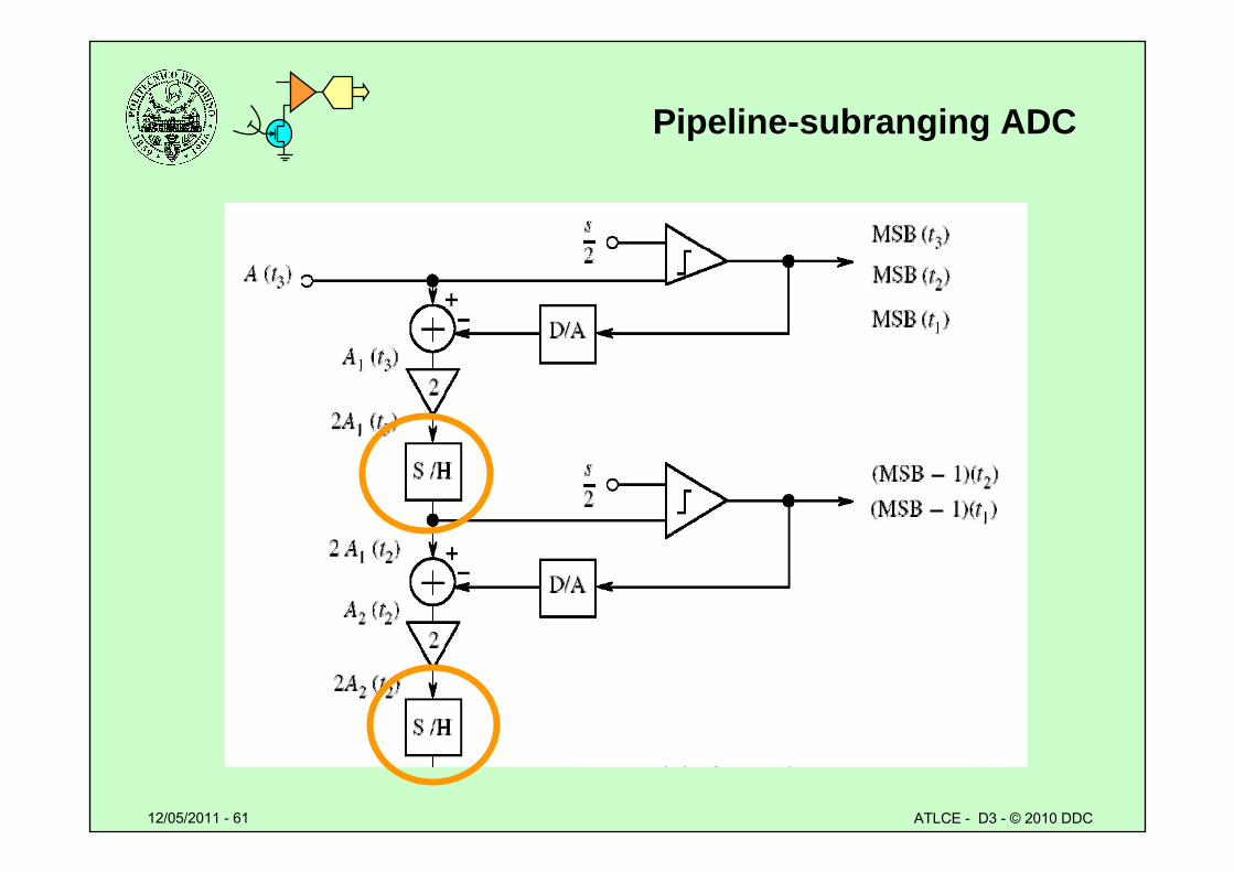
Pipeline-subranging ADC
12/05/2011 - 62 ATLCE - D3 - © 2010 DDC
Comparison with other techniques
• A N-bit pipeline A/D converter uses:– N comparators– N comparison cycles
(to complete the conversion of each sample)
• Conversion time:– N-cycle latency– 1-cycle conversion (throughput)
• Same speed as a flash with N comparators– (2N in the flash)
12/05/2011 - 63 ATLCE - D3 - © 2010 DDC
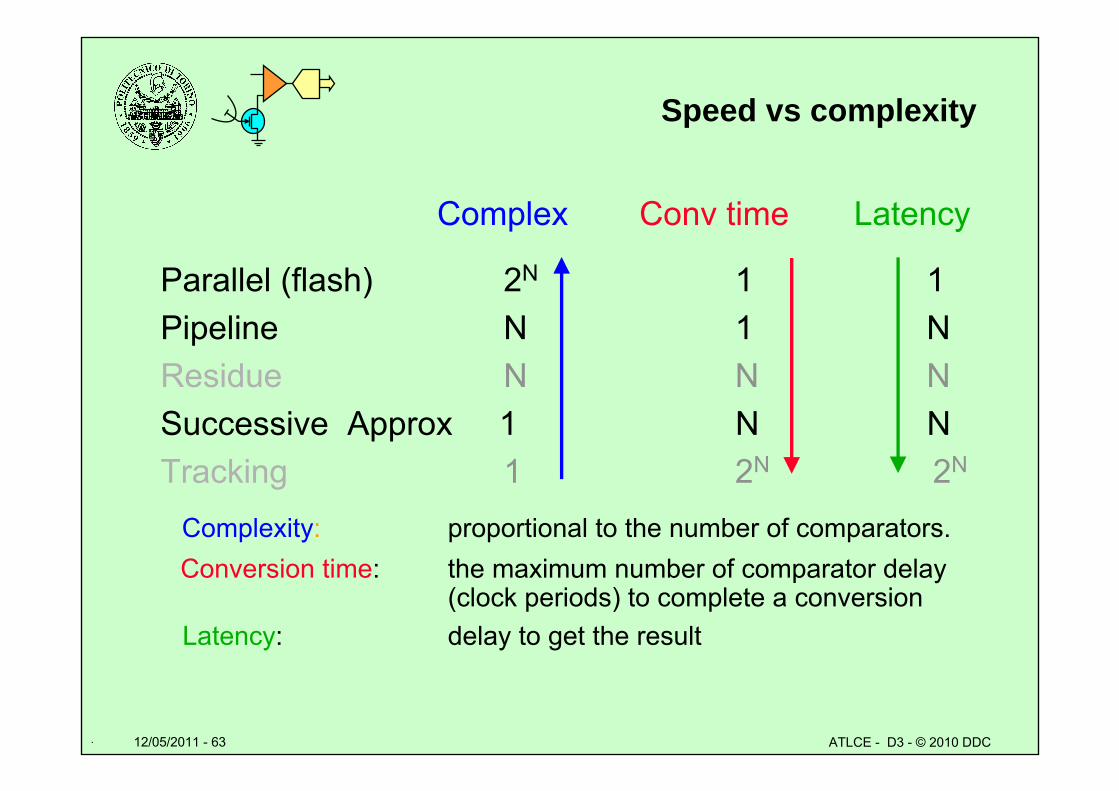
Speed vs complexity
Complex Conv time Latency
Parallel (flash) 2N 1 1Pipeline N 1 NResidue N N NSuccessive Approx 1 N NTracking 1 2N 2N
Complexity: proportional to the number of comparators.Conversion time: the maximum number of comparator delay
(clock periods) to complete a conversionLatency: delay to get the result
.
12/05/2011 - 64 ATLCE - D3 - © 2010 DDC
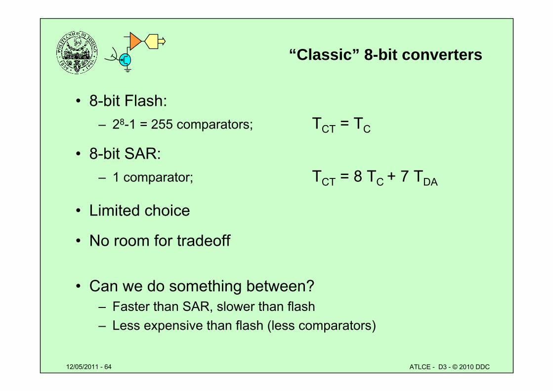
“Classic” 8-bit converters
• 8-bit Flash:– 28-1 = 255 comparators; TCT = TC
• 8-bit SAR:– 1 comparator; TCT = 8 TC + 7 TDA
• Limited choice
• No room for tradeoff
• Can we do something between?– Faster than SAR, slower than flash– Less expensive than flash (less comparators)
12/05/2011 - 65 ATLCE - D3 - © 2010 DDC
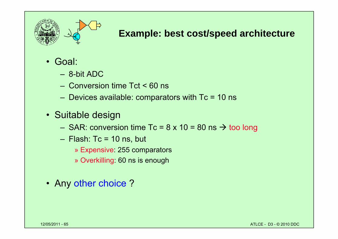
Example: best cost/speed architecture
• Goal:– 8-bit ADC– Conversion time Tct < 60 ns– Devices available: comparators with Tc = 10 ns
• Suitable design– SAR: conversion time Tc = 8 x 10 = 80 ns too long– Flash: Tc = 10 ns, but
» Expensive: 255 comparators» Overkilling: 60 ns is enough
• Any other choice ?
12/05/2011 - 66 ATLCE - D3 - © 2010 DDC
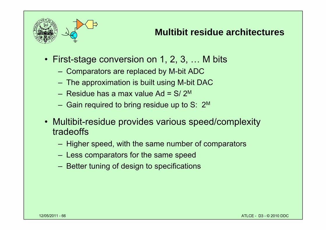
Multibit residue architectures
• First-stage conversion on 1, 2, 3, … M bits– Comparators are replaced by M-bit ADC– The approximation is built using M-bit DAC– Residue has a max value Ad = S/ 2M
– Gain required to bring residue up to S: 2M
• Multibit-residue provides various speed/complexity tradeoffs
– Higher speed, with the same number of comparators– Less comparators for the same speed– Better tuning of design to specifications
12/05/2011 - 67 ATLCE - D3 - © 2010 DDC
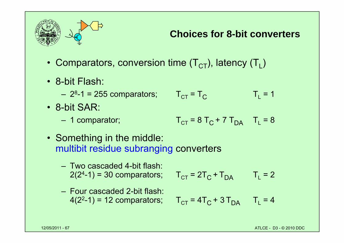
Choices for 8-bit converters
• Comparators, conversion time (TCT), latency (TL)
• 8-bit Flash:– 28-1 = 255 comparators; TCT = TC TL = 1
• 8-bit SAR:– 1 comparator; TCT = 8 TC + 7 TDA TL = 8
• Something in the middle: multibit residue subranging converters
– Two cascaded 4-bit flash: 2(24-1) = 30 comparators; TCT = 2TC + TDA TL = 2
– Four cascaded 2-bit flash: 4(22-1) = 12 comparators; TCT = 4TC + 3 TDA TL = 4
12/05/2011 - 68 ATLCE - D3 - © 2010 DDC
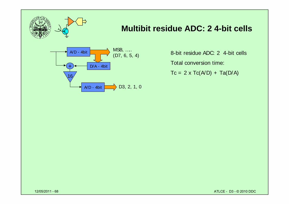
Multibit residue ADC: 2 4-bit cells
+
A/D - 4bit
D/A - 4bit
16
A/D - 4bit
MSB, …..(D7, 6, 5, 4)
D3, 2, 1, 0
8-bit residue ADC: 2 4-bit cells
Total conversion time:
Tc = 2 x Tc(A/D) + Ta(D/A)
12/05/2011 - 69 ATLCE - D3 - © 2010 DDC
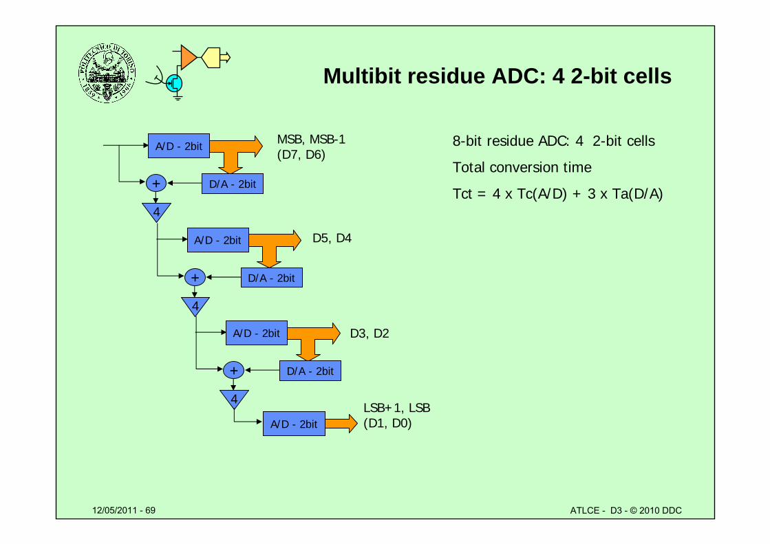
Multibit residue ADC: 4 2-bit cells
+
A/D - 2bit
D/A - 2bit
4
+
A/D - 2bit
D/A - 2bit
4
+
A/D - 2bit
D/A - 2bit
4
A/D - 2bit
MSB, MSB-1(D7, D6)
D5, D4
D3, D2
LSB+1, LSB(D1, D0)
8-bit residue ADC: 4 2-bit cells
Total conversion time
Tct = 4 x Tc(A/D) + 3 x Ta(D/A)
12/05/2011 - 70 ATLCE - D3 - © 2010 DDC
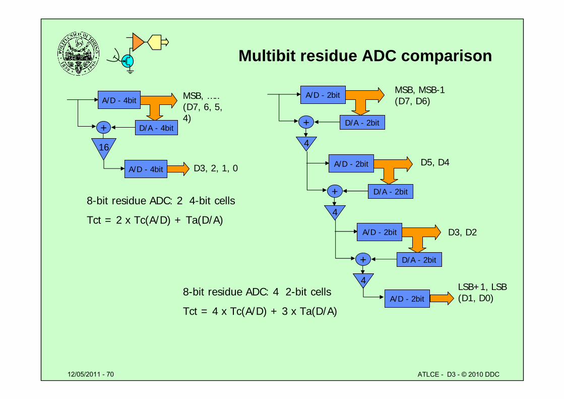
Multibit residue ADC comparison
+
A/D - 2bit
D/A - 2bit
4
+
A/D - 2bit
D/A - 2bit
4
+
A/D - 2bit
D/A - 2bit
4
A/D - 2bit
MSB, MSB-1(D7, D6)
D5, D4
D3, D2
LSB+1, LSB(D1, D0)
+
A/D - 4bit
D/A - 4bit
16
A/D - 4bit
MSB, …..(D7, 6, 5, 4)
D3, 2, 1, 0
8-bit residue ADC: 2 4-bit cells
Tct = 2 x Tc(A/D) + Ta(D/A)
8-bit residue ADC: 4 2-bit cells
Tct = 4 x Tc(A/D) + 3 x Ta(D/A)
12/05/2011 - 71 ATLCE - D3 - © 2010 DDC
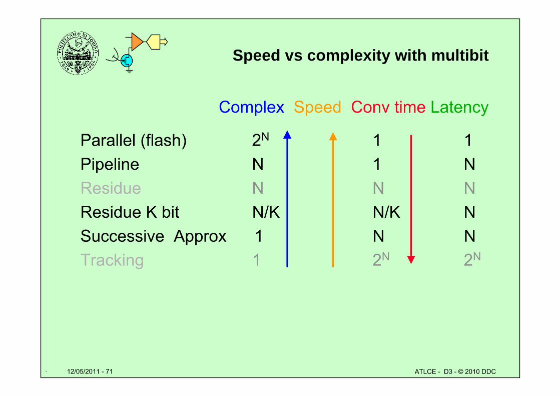
Speed vs complexity with multibit
Complex Speed Conv time Latency
Parallel (flash) 2N 1 1Pipeline N 1 NResidue N N NResidue K bit N/K N/K NSuccessive Approx 1 N NTracking 1 2N 2N
.
12/05/2011 - 72 ATLCE - D3 - © 2010 DDC
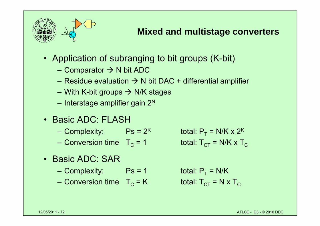
Mixed and multistage converters
• Application of subranging to bit groups (K-bit)– Comparator N bit ADC– Residue evaluation N bit DAC + differential amplifier– With K-bit groups N/K stages– Interstage amplifier gain 2N
• Basic ADC: FLASH– Complexity: Ps = 2K total: PT = N/K x 2K
– Conversion time TC = 1 total: TCT = N/K x TC
• Basic ADC: SAR– Complexity: Ps = 1 total: PT = N/K– Conversion time TC = K total: TCT = N x TC
12/05/2011 - 73 ATLCE - D3 - © 2010 DDC
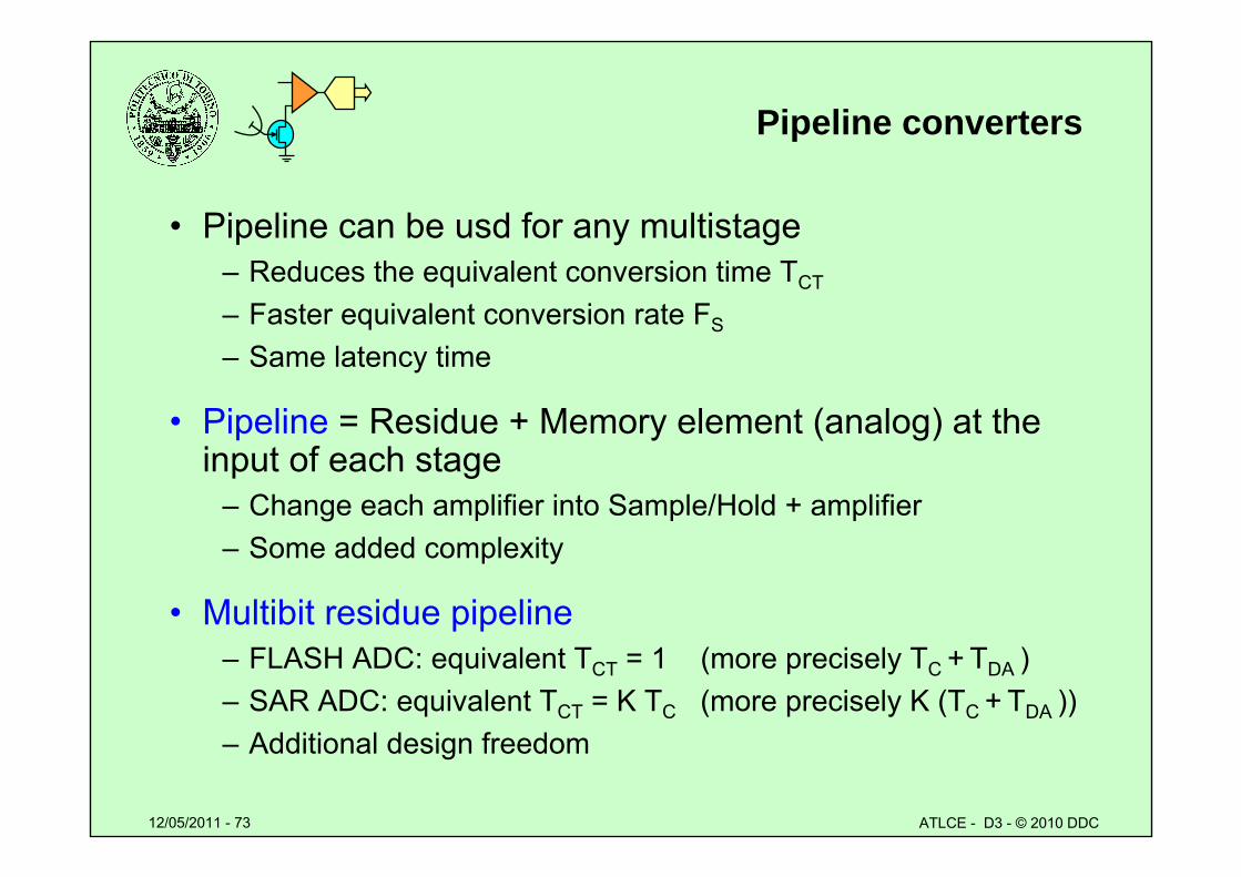
Pipeline converters
• Pipeline can be usd for any multistage– Reduces the equivalent conversion time TCT
– Faster equivalent conversion rate FS
– Same latency time
• Pipeline = Residue + Memory element (analog) at the input of each stage
– Change each amplifier into Sample/Hold + amplifier– Some added complexity
• Multibit residue pipeline– FLASH ADC: equivalent TCT = 1 (more precisely TC + TDA )– SAR ADC: equivalent TCT = K TC (more precisely K (TC + TDA ))– Additional design freedom
12/05/2011 - 74 ATLCE - D3 - © 2010 DDC
Speed vs complexity with multibit
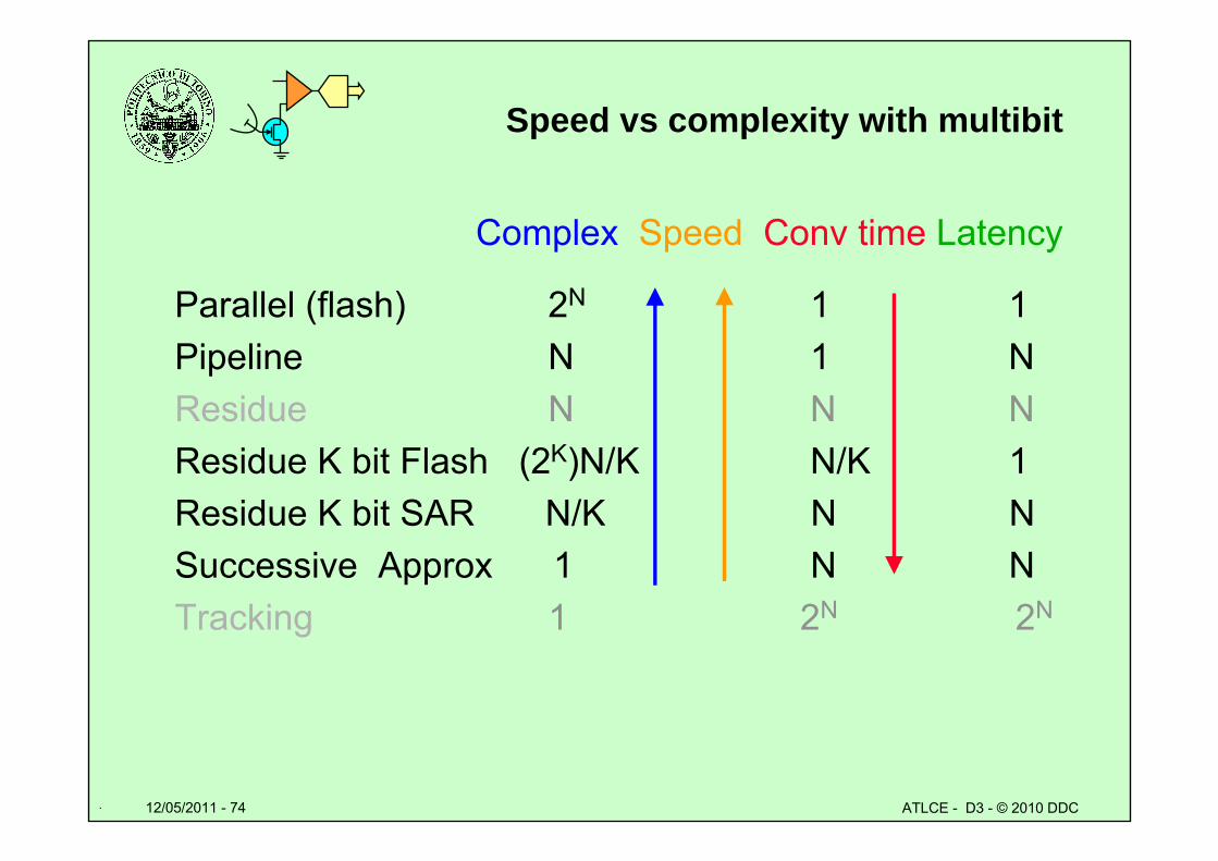
Complex Speed Conv time Latency
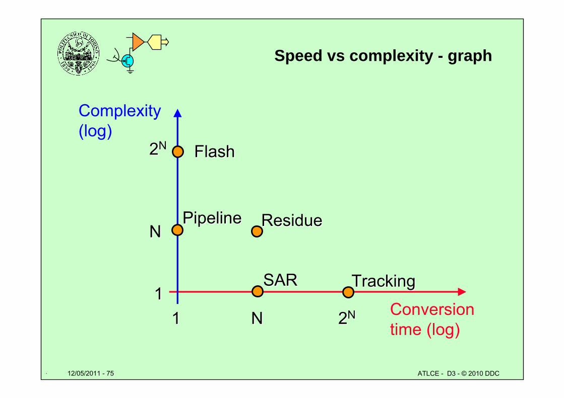
Parallel (flash) 2N 1 1Pipeline N 1 NResidue N N NResidue K bit Flash (2K)N/K N/K 1Residue K bit SAR N/K N NSuccessive Approx 1 N NTracking 1 2N 2N
.
12/05/2011 - 75 ATLCE - D3 - © 2010 DDC
Speed vs complexity - graph
.
Complexity(log)
Conversion time (log)
SARSAR
1 N 21 N 2NN
22NN
N N
11
FlashFlash
TrackingTracking
ResidueResiduePipelinePipeline
12/05/2011 - 76 ATLCE - D3 - © 2010 DDC
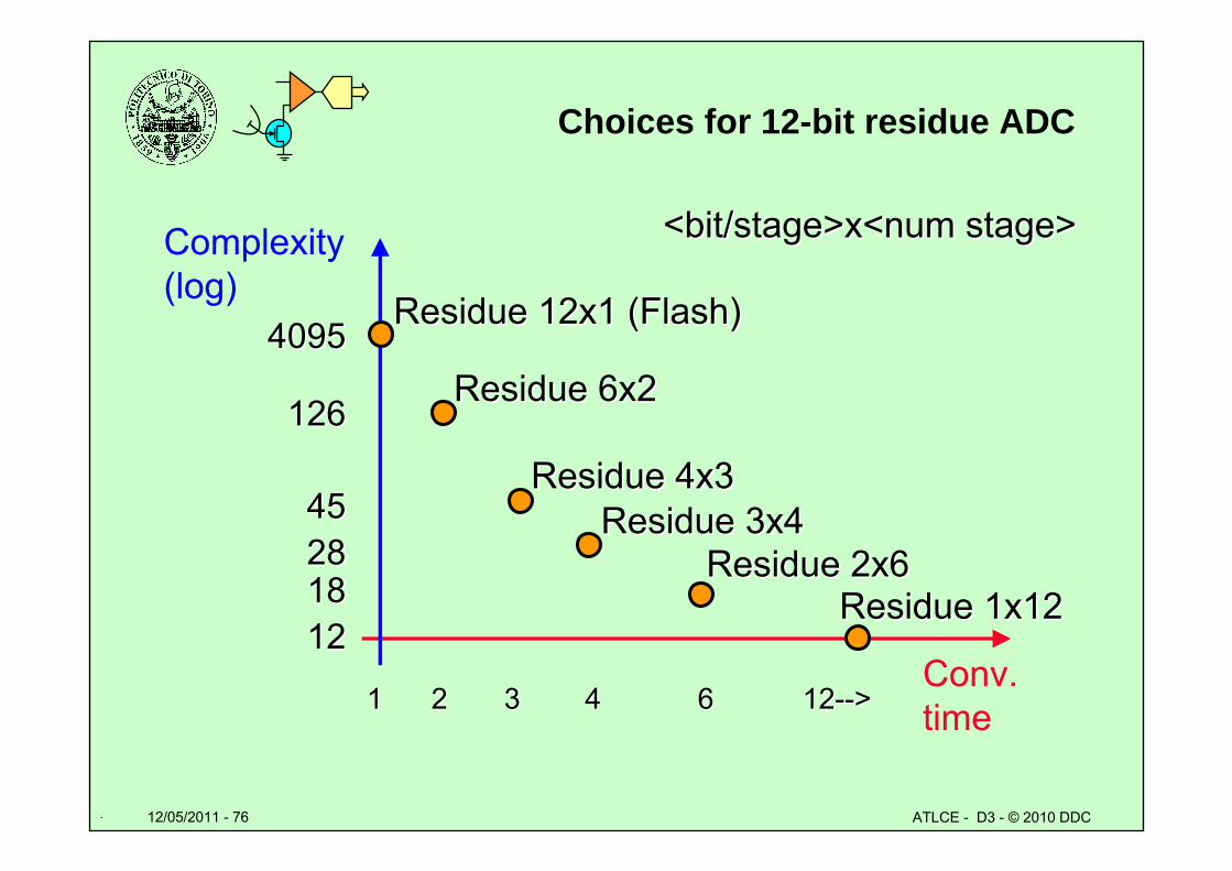
Choices for 12-bit residue ADC
.
Complexity(log)
Conv. time
<bit/stage>x<num stage><bit/stage>x<num stage>
1 2 3 4 6 121 2 3 4 6 12---->>
40954095
126126
45 45 282818181212
Residue 12x1 (Flash)Residue 12x1 (Flash)
Residue 6x2Residue 6x2
Residue 4x3Residue 4x3Residue 3x4Residue 3x4
Residue 2x6Residue 2x6Residue 1x12Residue 1x12
12/05/2011 - 77 ATLCE - D3 - © 2010 DDC
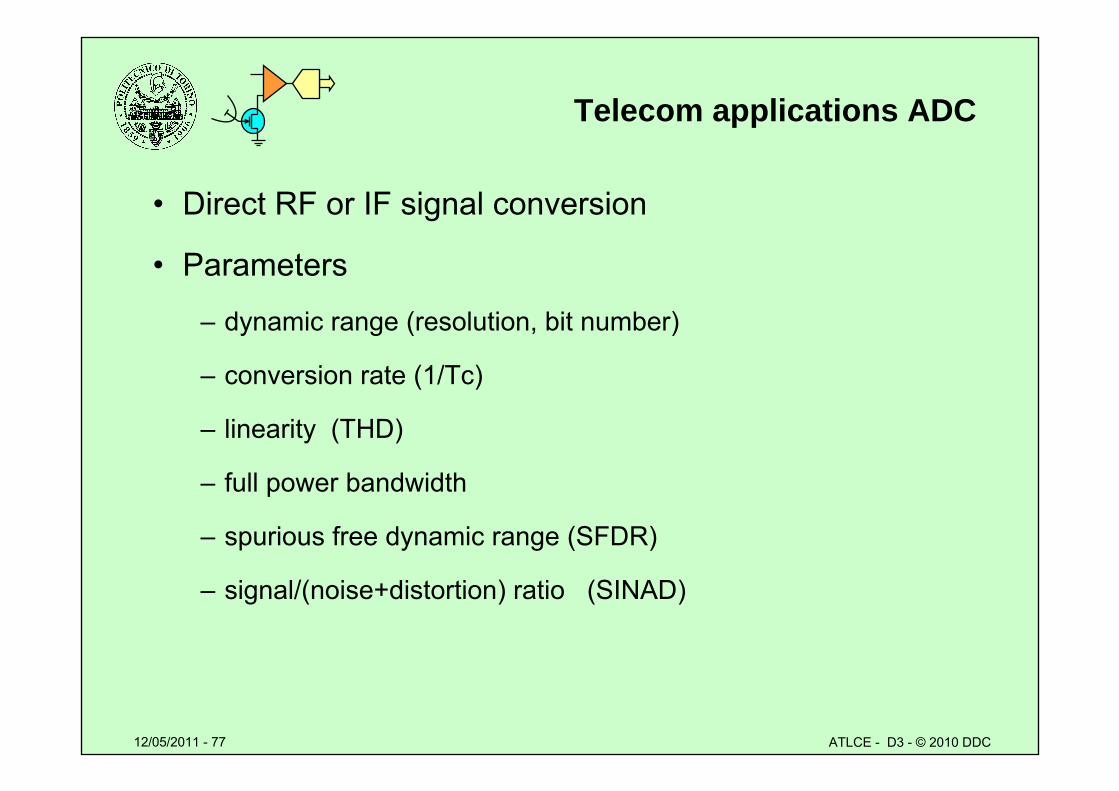
Telecom applications ADC
• Direct RF or IF signal conversion
• Parameters
– dynamic range (resolution, bit number)
– conversion rate (1/Tc)
– linearity (THD)
– full power bandwidth
– spurious free dynamic range (SFDR)
– signal/(noise+distortion) ratio (SINAD)
12/05/2011 - 78 ATLCE - D3 - © 2010 DDC
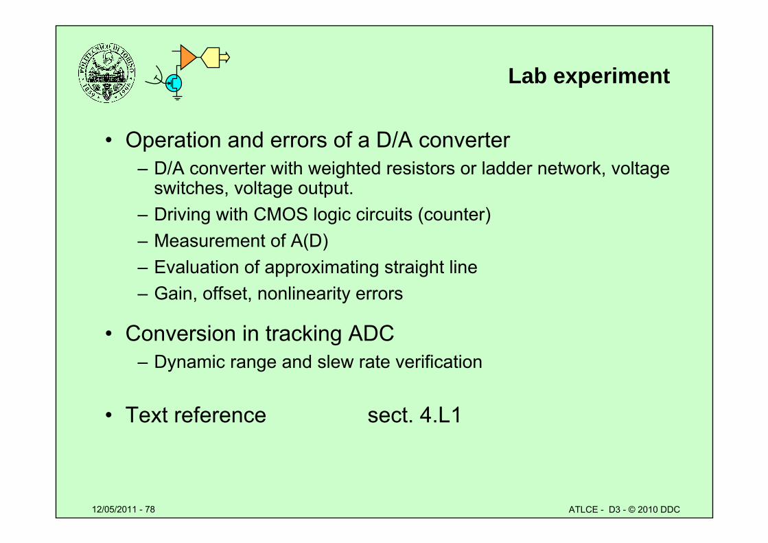
Lab experiment
• Operation and errors of a D/A converter– D/A converter with weighted resistors or ladder network, voltage
switches, voltage output.– Driving with CMOS logic circuits (counter)– Measurement of A(D)– Evaluation of approximating straight line– Gain, offset, nonlinearity errors
• Conversion in tracking ADC– Dynamic range and slew rate verification
• Text reference sect. 4.L1
12/05/2011 - 79 ATLCE - D3 - © 2010 DDC
Lesson D3 - final test
• Which is the effect of strong differential nonlinearity error?
• Describe the missed-code error.
• Which parameters can be used to classify ADCs?
• Draw the block diagram of a residue/subranging converter.
• Explain the difference between conversion time and latency.
• How many comparators are required for a 8-bit flash ADC?
• Which is the conversion delay (as number of comparator decision times) for a 8-bit SAR ADC?
• Draw the block diagram of a residue converter using 3 stages, with 3 bits each.