
AN9947: HC55185 and the IDT821068 Programmable Octal PCM CODEC
15
HC55185 and the IDT821068 Programmable Octal PCM CODEC APPLICATION NOTE AN9947 Rev 1.00 Page 1 of 15 Dec 4, 2001 AN9947 Rev 1.00 Dec 4, 2001 Reference Design using the HC55185 and the IDT821068 Programmable Octal PCM CODEC The purpose of this application note is to provide a reference design for the HC55185 and IDT821068 Programmable Octal PCM CODEC. The network requirements of many countries require the analog subscriber line circuit (SLIC) to terminate the subscriber line with an impedance for voiceband frequencies which is complex, rather than resistive (e.g. 600 . The HC55185 accomplishes this impedance matching with a single network connected between the VTX pin and the -IN pin. The IDT821068 Octal PCM CODEC uses an integrated programmable DSP to realize AC Impedance Matching, Transhybrid Balance, Frequency Response Correction and Gain Setting functions. Discussed in this application note are the following: • 2-wire impedance matching • Receive gain (4-wire to 2-wire) and transmit gain (2-wire to 4-wire) calculations • Reference design for both 600 and 200 +6800.1F (China Complex Impedance) Impedance Matching Impedance matching of the HC55185 to the subscriber load is important for optimization of 2-wire return loss, which in turn cuts down on echoes in the end to end voice communication path. Impedance matching of the HC55185 is accomplished by making the SLIC’s impedance (Z O , Figure 1) equal to the desired terminating impedance Z L , minus the value of the protection resistors (R P ). With the HC55185 programmed to match a ZL of 600, the IDT821068 uses an integrated programmable DSP to realize any AC impedance. The formula to program the HC55185 to match a 2-wire impedance of 600 is shown in Equation 1. The value of R S with 49 protection resistors is 66.9k. The closest standard value is 66.5k. SLIC in the Active Mode Figure 2 shows a simplified AC transmission model of the HC55185 and the connection of the IDT821068 to the SLIC. Circuit analysis of the HC55185 yields the following design equations: The Sense Amplifier is configured as a 4 input differential amplifier with a gain of 3/4. The voltage at the output of the sense amplifier (V SA ) is calculated using superposition. V SA 1 is the voltage resulting from V1, V SA 2 is the voltage resulting from V2 and so on (reference Figure 2). Where V is equal to I M R SENSE (R SENSE = 20) The voltage at VTX is equal to: V TR is defined in Figure 2, note polarity assigned to V TR : R S 133.3 Z L 2R P – 133.3 600 2R P – = = (EQ. 1) V SA 1 3 4 -- V 1 – = (EQ. 2) V SA 2 3 4 -- V 2 = (EQ. 3) V SA 3 3 4 -- V 3 – = (EQ. 4) V SA 4 3 4 -- V 4 = (EQ. 5) V SA V 2 V 1 – V 4 V 3 – + 3 4 -- V V + 3 4 -- = = (EQ. 6) V SA 2 I M 20 3 4 -- I M 30 = = (EQ. 7) V TX V SA – R S 8K ------- R S 8K ------- I M 30 – = = (EQ. 8) V TR 2V RX V TX + = (EQ. 9) FIGURE 1. IMPEDANCE MATCHING TIP RING V RX Z L V 2W E G Z O Z TR V TR + - + - R S V TX VFB R S R P 49 R P 49 RESISTIVE Z L = Z TR = 600 R S = 133.3(600 - 2*49) R S 66.9k INTERSIL HC55185 STD VALUE 66.5k -IN C TX C FB Z O = Z L - 2 RP 66.5k 4.7F 0.47F C RX 0.47F
Transcript of AN9947: HC55185 and the IDT821068 Programmable Octal PCM CODEC

HC55185 and the IDT821068 Programmable Octal PCM CODEC
APPLICATION NOTE
AN9947Rev 1.00
Dec 4, 2001
Reference Design using the HC55185 and the IDT821068 Programmable Octal PCM CODECThe purpose of this application note is to provide a reference design for the HC55185 and IDT821068 Programmable Octal PCM CODEC.
The network requirements of many countries require the analog subscriber line circuit (SLIC) to terminate the subscriber line with an impedance for voiceband frequencies which is complex, rather than resistive (e.g. 600 . The HC55185 accomplishes this impedance matching with a single network connected between the VTX pin and the -IN pin.
The IDT821068 Octal PCM CODEC uses an integrated programmable DSP to realize AC Impedance Matching, Transhybrid Balance, Frequency Response Correction and Gain Setting functions.
Discussed in this application note are the following:
• 2-wire impedance matching
• Receive gain (4-wire to 2-wire) and transmit gain (2-wire to 4-wire) calculations
• Reference design for both 600 and 200 +6800.1F (China Complex Impedance)
Impedance MatchingImpedance matching of the HC55185 to the subscriber load is important for optimization of 2-wire return loss, which in turn cuts down on echoes in the end to end voice communication path. Impedance matching of the HC55185 is accomplished by making the SLIC’s impedance (ZO, Figure 1) equal to the desired terminating impedance ZL, minus the value of the protection resistors (RP).
With the HC55185 programmed to match a ZL of 600, the IDT821068 uses an integrated programmable DSP to realize
any AC impedance. The formula to program the HC55185 to match a 2-wire impedance of 600is shown in Equation 1.
The value of RS with 49protection resistors is 66.9k. The closest standard value is 66.5k.
SLIC in the Active ModeFigure 2 shows a simplified AC transmission model of the HC55185 and the connection of the IDT821068 to the SLIC. Circuit analysis of the HC55185 yields the following design equations:
The Sense Amplifier is configured as a 4 input differential amplifier with a gain of 3/4. The voltage at the output of the sense amplifier (VSA) is calculated using superposition. VSA1 is the voltage resulting from V1, VSA2 is the voltage resulting from V2 and so on (reference Figure 2).
Where V is equal to IMRSENSE (RSENSE = 20)
The voltage at VTX is equal to:
VTR is defined in Figure 2, note polarity assigned to VTR:
RS 133.3 ZL 2RP– 133.3 600 2RP– == (EQ. 1)
VSA1 34--- V1 –= (EQ. 2)
VSA2 34--- V2 = (EQ. 3)
VSA3 34--- V3 –= (EQ. 4)
VSA4 34--- V4 = (EQ. 5)
VSA V2 V1– V4 V3– + 34--- V V+ 3
4---= = (EQ. 6)
VSA 2 IM 20 34--- IM30= = (EQ. 7)
VTX VSA–RS8K-------- RS
8K-------- IM30–= = (EQ. 8)
VTR 2 VRX VTX+ = (EQ. 9)
FIGURE 1. IMPEDANCE MATCHING
TIP
RING
VRX
ZLV2W
EG
ZOZTR
VTR
+
-
+
- RS
VTX
VFB
RSRP49
RP49
RESISTIVE
ZL = ZTR = 600
RS = 133.3(600 - 2*49)
RS
66.9k
INTERSILHC55185
STD VALUE66.5k
-IN
CTX
CFB
ZO = ZL - 2RP
66.5k
4.7F
0.47F
CRX 0.47F
AN9947 Rev 1.00 Page 1 of 15Dec 4, 2001

HC55185 and the IDT821068
Programmable Octal PCM CODEC
Setting VRX equal to zero, substituting Equation 8 into Equation 9 and defining ZO = -VTR/IM will enable the user to determine the require feedback to match the line impedance at V2W.
ZO is the source impedance of the device and is defined as ZO = ZL - 2Rp. ZL is the line impedance. RS is defined as:
Substitute Equation 8 into Equation 12
Substitute Equation 13 into Equation 14
Substitute Equation 10 for RS and -V2w/ZL for IM into Equation 15.
Substitute Equation 16 into Equation 17 and combine terms
where:
VRX = The input voltage at the VRX pin.
VSA = An internal node voltage that is a function of the loop current and the output of the Sense Amplifier.
IX = Internal current in the SLIC that is the difference between the input receive current and the feedback current.
IM = The AC metallic current.
RP = A protection resistor (typical 49.9).
RS = An external resistor/network for matching the line impedance.
VTR = The tip to ring voltage at the output pins of the SLIC.
V2W = The tip to ring voltage including the voltage across the protection resistors.
ZL = The line impedance.
ZO = The source impedance of the device.
ZO1
133.33------------------RS= (EQ. 10)
RS 133.33 ZL 2RP– = (EQ. 11)
IXVRX
R----------- +
VTXR
-----------=
Node Equation
(EQ. 12)
at HC55185 VRX input
IXVRX
R-----------
RS IM30
R8K------------------------- –= (EQ. 13)
IXR - VTR + IXR = 0
Loop Equation(EQ. 14)
at HC55185 feed amplifiers and load
VTR 2VRX
RS IM60
8K------------------------- –= (EQ. 15)
VTR 2VRX
ZOV2WZL
--------------------+= (EQ. 16)
V2W -IM2RP + VTR = 0
Loop Equation(EQ. 17)
at Tip/Ring interface
V2W
ZL ZO 2RP+ +
ZL-------------------------------------- 2VRX–= (EQ. 18)
VRXTIP
RING
EG
VTR
IM VTX
RP
RP
+
-
+
-
-
+
VRX+
-
IM
ZL
FIGURE 2. HC55185 SIMPLIFIED AC TRANSMISSION CIRCUIT AND IDT821068
+-
R
+-
R
RSENSE
+ -
VSA = IM30
IX
IX+-
IX+ -
+ -
+-
IM
+
-
20
20
V2W
+
-
VIN
DR1/DD
DX1/DU
IDT821068 INTERSIL
HC55185 (1 OF 8)
VTX
Z0
1:1
+-
CFB
VFB
-IN
TA
R
R
RS
8k
3R
3R
4R
4R
4R
4R
IX
SENSE AMPLIFIER
FEEDBACK AMPLIFIER
RECEIVE BLOCK
V1V2
V3 V4
IM +-
IM+ -
RSENSE D/A ANDVOUT1
DSPCORE
CHANNEL 1
CHANNEL 2
CHANNEL 3
CHANNEL 4
CHANNEL 5
CHANNEL 6
CHANNEL 7
CHANNEL 8
VIN1AMPLIFIERFEED
AMPLIFIERFEED
FILTER
PCM/GCIINTER-FACE
FILTERAND A/D
AN9947 Rev 1.00 Page 2 of 15Dec 4, 2001
HC55185 and the IDT821068
Programmable Octal PCM CODEC
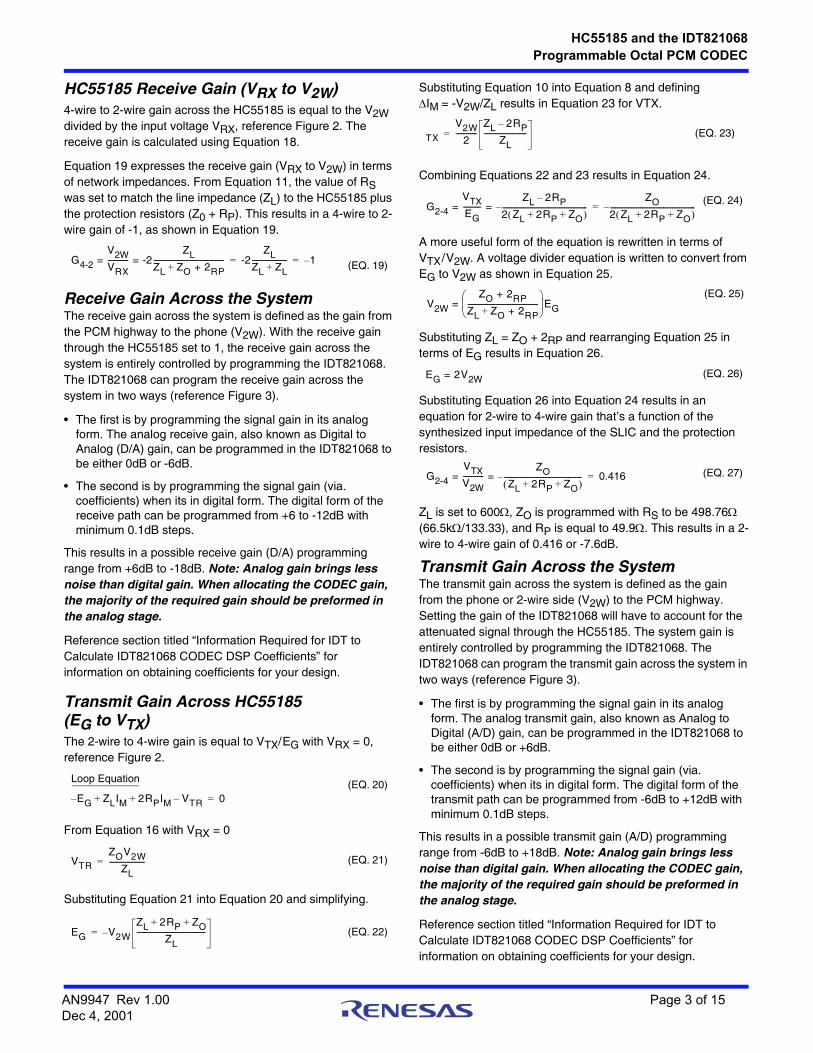
HC55185 Receive Gain (VRX to V2W)4-wire to 2-wire gain across the HC55185 is equal to the V2W divided by the input voltage VRX, reference Figure 2. The receive gain is calculated using Equation 18.
Equation 19 expresses the receive gain (VRX to V2W) in terms of network impedances. From Equation 11, the value of RS was set to match the line impedance (ZL) to the HC55185 plus the protection resistors (Z0 + RP). This results in a 4-wire to 2-wire gain of -1, as shown in Equation 19.
Receive Gain Across the SystemThe receive gain across the system is defined as the gain from the PCM highway to the phone (V2W). With the receive gain through the HC55185 set to 1, the receive gain across the system is entirely controlled by programming the IDT821068. The IDT821068 can program the receive gain across the system in two ways (reference Figure 3).
• The first is by programming the signal gain in its analog form. The analog receive gain, also known as Digital to Analog (D/A) gain, can be programmed in the IDT821068 to be either 0dB or -6dB.
• The second is by programming the signal gain (via. coefficients) when its in digital form. The digital form of the receive path can be programmed from +6 to -12dB with minimum 0.1dB steps.
This results in a possible receive gain (D/A) programming range from +6dB to -18dB. Note: Analog gain brings less noise than digital gain. When allocating the CODEC gain, the majority of the required gain should be preformed in the analog stage.
Reference section titled “Information Required for IDT to Calculate IDT821068 CODEC DSP Coefficients” for information on obtaining coefficients for your design.
Transmit Gain Across HC55185(EG to VTX)The 2-wire to 4-wire gain is equal to VTX/EG with VRX = 0, reference Figure 2.
From Equation 16 with VRX = 0
Substituting Equation 21 into Equation 20 and simplifying.
Substituting Equation 10 into Equation 8 and definingIM = -V2W/ZL results in Equation 23 for VTX.
Combining Equations 22 and 23 results in Equation 24.
A more useful form of the equation is rewritten in terms of VTX/V2W. A voltage divider equation is written to convert from EG to V2W as shown in Equation 25.
Substituting ZL = ZO + 2RP and rearranging Equation 25 in terms of EG results in Equation 26.
Substituting Equation 26 into Equation 24 results in an equation for 2-wire to 4-wire gain that’s a function of the synthesized input impedance of the SLIC and the protection resistors.
ZL is set to 600, ZO is programmed with RS to be 498.76 (66.5k/133.33), and RP is equal to 49.9. This results in a 2-wire to 4-wire gain of 0.416 or -7.6dB.
Transmit Gain Across the SystemThe transmit gain across the system is defined as the gain from the phone or 2-wire side (V2W) to the PCM highway. Setting the gain of the IDT821068 will have to account for the attenuated signal through the HC55185. The system gain is entirely controlled by programming the IDT821068. The IDT821068 can program the transmit gain across the system in two ways (reference Figure 3).
• The first is by programming the signal gain in its analog form. The analog transmit gain, also known as Analog to Digital (A/D) gain, can be programmed in the IDT821068 to be either 0dB or +6dB.
• The second is by programming the signal gain (via. coefficients) when its in digital form. The digital form of the transmit path can be programmed from -6dB to +12dB with minimum 0.1dB steps.
This results in a possible transmit gain (A/D) programming range from -6dB to +18dB. Note: Analog gain brings less noise than digital gain. When allocating the CODEC gain, the majority of the required gain should be preformed in the analog stage.
Reference section titled “Information Required for IDT to Calculate IDT821068 CODEC DSP Coefficients” for information on obtaining coefficients for your design.
G4-2 = V2WVRX------------ = -2
ZLZL ZO+ + 2RP---------------------------------------- -2
ZLZL ZL+-------------------- 1–= = (EQ. 19)
E– G ZLIM 2RPIM VTR–++ 0=
Loop Equation(EQ. 20)
VTR
ZOV2WZL
--------------------= (EQ. 21)
EG V2W
ZL 2RP ZO+ +
ZL---------------------------------------–= (EQ. 22)
VTX
V2W2
------------ZL 2RP–
ZL------------------------= (EQ. 23)
G2-4 = VTXEG---------- =
ZL 2RP–
2 ZL 2RP ZO+ + ------------------------------------------------–
ZO2 ZL 2RP ZO+ + ------------------------------------------------–=
(EQ. 24)
V2W = ZO + 2RP
ZL ZO+ + 2RP----------------------------------------
EG
(EQ. 25)
EG = 2V2W (EQ. 26)
G2-4 = VTXV2W------------ =
ZOZL 2RP ZO+ + --------------------------------------------– 0.416= (EQ. 27)
AN9947 Rev 1.00 Page 3 of 15Dec 4, 2001

HC55185 and the IDT821068
Programmable Octal PCM CODEC
Transhybrid Balance G(4-4)Transhybrid balance is a measure of how well the input signal is canceled (that being received by the SLIC) from the transmit signal (that being transmitted from the SLIC to the CODEC). Without this function, voice communication would be difficult because of the echo. The Transhybrid balancing filter inside the IDT821068 is used to adjust transhybrid balance to ensure the echo cancellation meets the ITU-T specifications. The coefficient for Echo Cancellation is ECF.
Frequency Response CorrectionThe FRR filter in the receive path and the FRX filter in the transmit path can be programmed to correct any frequency distortion caused by the impedance matching filters. The coefficients of Frequency Response Correction are FRR for receive path and FRX for the transmit path.
Information Required for IDT to Calculate IDT821068 CODEC DSP CoefficientsFor IDT to calculate IDT821068 DSP coefficient, customers should provide the following information about their subscriber line card:
• Accurate SLIC PSPICE model. It can be provided in .lib file or PSPICE schematic file.
• System Impedance
• Gain (Transmit path and Receive path)
Using the DSP coefficients provided by IDT, the overall performance of the system will pass ITU-T requirements.
When the COF RAM button is selected from the MPI Operation General Interface screen, the COF RAM Operation screen will appear (Figure 4). From this screen, the user can configure all the coefficients for the current channel.
Reference Design of the HC55185 and the IDT821068 With a 600 LoadThe design criteria is as follows:
• 4-wire to 2-wire gain (DR1/DD to V2W) equal 0dB
• 2-wire to 4-wire gain (V2W to DX1/DU) equal 0dB
• Rp = 49.9
Figure 5 gives the reference design using the Intersil HC55185 and the IDT821068 Programmable Octal PCM CODEC. Also shown in Figure 5 are the voltage levels at specific points in the circuit.
Impedance MatchingThe 2-wire impedance is matched to the line impedance Z0 using Equation 1, repeated here in Equation 28.
For a line impedance of 600, RS equals:
The closest standard value for RS would be 66.5k .
FIGURE 3. RECEIVE GAIN G(4-2), TRANSMIT GAIN (2-4)
TIP
RING
INTERSIL
VRX
HC55185 (1 OF 8)
ZLV2W
EG
ZOZTR
VTR
+
-
+
-
RP49
RP49
ZO = ZL - 2RP
RS
VTX
VFB
-IN
CTX
CFB
0.47F
4.7F
0.47F
DR1/DD
DX1/DU
IDT821068
VOUT1
DSPCORE
CHANNEL 1
CHANNEL 2
CHANNEL 8
VIN1
...
ANALOGGAIN
0dB TO -6dB
ANALOGGAIN
0dB TO +6dB
RECEIVE PATH
TRANSMIT PATH
FRRFILTER
FRXFILTER
CRXDIGITAL
GAIN+6dB TO -12dB
DIGITALGAIN
-6dB TO +12dB
PCM/GCIINTERFACE
FIGURE 4. COEFFICIENT RAM OPERATION SCREEN
RS 133.3 ZL 2RP– = (EQ. 28)
RS 133.3 600 98– 66.9k= = (EQ. 29)
AN9947 Rev 1.00 Page 4 of 15Dec 4, 2001

HC55185 and the IDT821068
Programmable Octal PCM CODEC
However, it would be very convenient and cost effective if system manufacturers can use only one type of line card to meet different impedance requirements and different gain requirements. The programmability of IDT821068 can help system manufactures to reach this goal. By using different coefficients and tweaking the value of RS, this reference design can meet both 600 and 200 + 6800.1F impedance requirements. To obtain the best results, RS should be an optimized value. By experimental experience, it is recommended to set RS = 90.9k 1%
With the optimized value of RS selected to be 90.9k 1%, the coefficients for different Transmit Gains (A/D) and Receive Gains (with a line impedance of 600) are given in Tables 1, 2 and 3.
Although the impedance matching resistor (RS) of the HC55185 has been changed, the contribution from the IDT821068 allows the system to still match the load. With the load matched, the 2-wire to 4-wire gain (Equation 27) is still equal to -7.6dB.
Specific Implementation for ChinaThe design criteria for a China specific solution are as follows:
• Desired line circuit impedance is 200 + 680//0.1F
• Receive gain (V2W/(DR1/DD)) is -3.5dB
• Transmit gain ((DX1/DU)/V2W) is 0dB
• 0dBm0 is defined as 1mW into the complex impedance at 1020Hz
• Rp = 49.9
Figure 6 gives the reference design using the Intersil HC55185 and the IDT821068 Programmable Octal PCM CODEC. Also shown in Figure 6 are the voltage levels at specific points in the circuit. Note: The transmit gain of the system is 0dB (-2.19dB(811) = -3.5dB(600)) as explained in the following section.
Adjustment to Get -3.5dBm0 at the Load Referenced to 600The voltage equivalent to 0dBm0 into 811 (0dBm0(811) is calculated using Equation 30 (811 is the impedance of complex China load at 1020Hz).
The gain referenced back to 0dBm0(600 is equal to:
The adjustment to get -3.5dBm0 at the load referenced to 600 is:
The voltage at the load (referenced to 600) is given in Equation 33:
NOTE: Reference Table 1 for coefficients.
FIGURE 5. REFERENCE DESIGN OF THE HC55185 AND THE IDT821068 WITH A 600 LOAD IMPEDANCE
PCMBUS
0dBm0(600)
0.7745VRMS0dBm0(600)
0.7745VRMS
0dBm0(600)
0.7745VRMS
0dBm0(600)
0.7745VRMS
0dBm0(600)
0.7745VRMS
G4-2
G2-4
-7.5769dBm0(600)
0.3239VRMS
TIP
RING
INTERSIL
VRX
HC55185 (1 OF 8)
ZLV2W
EG
ZOZTR
VTR
+
-
+
-
RP49
RP49
ZO = ZL - 2RPRS
VTX
VFB
-IN
CTX
CFB
0.47F
4.7F
0.47F
DR1/DD
DX1/DU
IDT821068
VOUT1
PCM/GCIINTERFACE
DSPCORE
CHANNEL 1
CHANNEL 2
CHANNEL 8
VIN1
...
RECEIVE PATH
TRANSMIT PATH
90.9k
CRX
SYSTEM REQUIREMENTS:IMPEDANCE: 600TRANSMIT GAIN (A/D): 0dBRECEIVE GAIN (D/A): 0dB
DIGITALGAIN0dB
DIGITALGAIN
+1.6dB
ANALOGGAIN0dB
ANALOGGAIN6dB
0dBm 811 10 V2
811 0.001 ------------------------------log 0.90055VRMS= = (EQ. 30)
GAIN 200.90055VRMS0.7745VRMS--------------------------------------log 1.309dB= = (EQ. 31)
Adjustment 3.5dBm0– 1.309dBm0+ 2.19– dB= = (EQ. 32)
2.19– dBm 600 10 V2
600 0.001 ------------------------------log 0.60196VRMS= = (EQ. 33)
AN9947 Rev 1.00 Page 5 of 15Dec 4, 2001

HC55185 and the IDT821068
Programmable Octal PCM CODEC
Impedance MatchingWith the optimized value of RS selected to be 90.9k 1%, the coefficients for different Transmit Gains (A/D) and Receive
Gains (with a line impedance of 200+ 6800.1F) are given in Tables 4, 5 and 6.
NOTE: Reference Table 5 for coefficients.
FIGURE 6. REFERENCE DESIGN OF THE HC55185 AND THE IDT821068 WITH CHINA COMPLEX LOAD IMPEDANCE
-2.19dBm0(600)-2.19dBm0(600)
0.60196VRMS
-2.19dBm0(600)
0.60196VRMS
G4-2
G2-4
VPWRO+
VPCMOUT
0.60196VRMS
0dBm0(600)0.7745VRMS
0.51769VRMS
-3.5dBm0(600)-9.3294dBm0(600)
0.26461RMS
TIP
RING
INTERSIL
VRX
HC55185
ZLV2W
EG
ZOZTR
VTR
+
-
+
-
RP49
RP49
ZO = ZL - 2RP
0.47F
DR1/DD
DX1/DU
IDT821068
VOUT1
DSPCORE
CHANNEL 1
CHANNEL 2
CHANNEL 8
VIN1
...
ANALOGGAIN0dB
DIGITALGAIN
-2.19dB
ANALOGGAIN+6dB
DIGITALGAIN
+1.6dB
RECEIVE PATH
TRANSMIT PATH
CRX
SYSTEM REQUIREMENTS:IMPEDANCE: 200+600||0.1FTRANSMIT GAIN (A/D): 0dBRECEIVE GAIN (D/A): -3.5dB
RS
VTX
VFB
-IN
CTX
CFB4.7F
0.47F90.9k
PCM/GCIINTERFACE
TABLE 1. 600 COEFFICIENTS, SYSTEM GAINS: (TRANSMIT GAIN (0dB), RECEIVE GAIN (0dB)),CODEC ANALOG GAINS: (TRANSMIT PATH +6dB, RECEIVE PATH 0dB)
COEFFICIENT RAM CHANNEL 1
IMF: 43 FD 90 EC 92 26 8A EF FF 7F 00 00 00 00 00 00
ECF: FB 00 8F FF 97 FE 5A 07 23 1B C1 1E 2F F9 00 00
KM: 00 00 00 00 00 00 00 00 00 00 00 00 00 00 E0 11
ACT: DD FF 33 FE AD 42 AD 42 33 FE DD FF CD AC GTX FF 1F
ACR: BF 00 36 FD 6A 42 6A 42 36 FD BF 00 01 88 GRX FA 02
COEFFICIENT RAM CHANNEL 2
IMF: 6C FC 85 EE 1A 25 E3 EF FF 7F 00 00 00 00 00 00
ECF: 9D 00 F5 FF 1F FF 9C 04 AD 1A 7C 23 9F F7 00 00
KM: 00 00 00 00 00 00 00 00 00 00 00 00 00 00 E0 11
ACT: 8C FF 6D FE 8C 42 8C 42 6D FE 8C FF CD C0 GTX A1 1F
ACR: E6 00 EA FC 94 42 94 42 EA FC E6 00 01 88 GRX F1 02
COEFFICIENT RAM CHANNEL 3
IMF: 69 FD BB EB DB 27 FB EE FE 7F 00 00 00 00 00 00
ECF: BE 01 CD FE 30 FF 62 02 28 19 76 2C 26 F3 00 00
KM: 00 00 00 00 00 00 00 00 00 00 00 00 00 00 E0 11
ACT: C5 FF CF FD 01 43 01 43 CF FD C5 FF CD AC GTX A1 1F
ACR: E8 00 92 FC DC 42 DC 42 92 FC E8 00 01 88 GRX FA 02
AN9947 Rev 1.00 Page 6 of 15Dec 4, 2001

HC55185 and the IDT821068
Programmable Octal PCM CODEC
COEFFICIENT RAM CHANNEL 4
IMF: 2F FD EC EB 2A 28 B5 EE FF 7F 00 00 00 00 00 00
ECF: 35 01 70 FF B0 FF 8C 00 F1 17 41 31 44 F1 00 00
KM: 00 00 00 00 00 00 00 00 00 00 00 00 00 00 E0 11
ACT: C3 FF AB FD 1A 43 1A 43 AB FD C3 FF CD AC GTX A1 1F
ACR: 0C 01 29 FC 1D 43 1D 43 29 FC 0C 01 01 88 GRX FA 02
COEFFICIENT RAM CHANNEL 5
IMF: 01 FB 72 F0 8D 25 F8 EE FF 7F 00 00 00 00 00 00
ECF: BE FE D4 02 EB FF 07 FE 4A 11 CC 41 3B EA 00 00
KM: 00 00 00 00 0 00 00 00 00 00 00 00 00 00 E0 11
ACT: ED FF 79 FD 2E 43 2E 43 79 FD ED FF CD AC GTX A1 1F
ACR: 1A 01 24 FC 22 43 22 43 24 FC 1A 01 01 88 GRX F1 02
COEFFICIENT RAM CHANNEL 6
IMF: 01 FB 72 F0 8D 25 F8 EE FF 7F 00 00 00 00 00 00
ECF: BE FE D4 02 EB FF 07 FE 4A 11 CC 41 3B EA 00 00
KM: 00 00 00 00 0 00 00 00 00 00 00 00 00 00 E0 11
ACT: B2 FF 64 FD 5A 43 5A 43 64 FD B2 FF CD AC GTX FF 1F
ACR: 39 01 BC FB 72 43 72 43 BC FB 39 01 01 88 GRX F1 02
COEFFICIENT RAM CHANNEL 7
IMF: 01 FB 72 F0 8D 25 F8 EE FF 7F 00 00 00 00 00 00
ECF: BE FE D4 02 EB FF 07 FE 4A 11 CC 41 3B EA 00 00
KM: 00 00 00 00 0 00 00 00 00 00 00 00 00 00 E0 11
ACT: AB FF 46 FD 77 43 77 43 46 FD AB FF CD AC GTX FF 1F
ACR: 3C 01 66 FB A9 43 A9 43 66 FB 3C 01 01 88 GRX F1 02
COEFFICIENT RAM CHANNEL 8
IMF: 01 FB 72 F0 8D 25 F8 EE FF 7F 00 00 00 00 00 00
ECF: BE FE D4 02 EB FF 07 FE 4A 11 CC 41 3B EA 00 00
KM: 00 00 00 00 0 00 00 00 00 00 00 00 00 00 E0 11
ACT: 77 FF 32 FD C1 43 C1 43 32 FD 77 FF CD AC GTX FF 1F
ACR: 2A 01 2C FB DE 43 DE 43 2C FB 2A 01 01 88 GRX FA 02
TABLE 1. 600 COEFFICIENTS, SYSTEM GAINS: (TRANSMIT GAIN (0dB), RECEIVE GAIN (0dB)),CODEC ANALOG GAINS: (TRANSMIT PATH +6dB, RECEIVE PATH 0dB) (Continued)
TABLE 2. 600 COEFFICIENTS, SYSTEM GAINS: (TRANSMIT GAIN (0dB), RECEIVE GAIN (-3.5dB)), CODEC ANALOG GAINS: (TRANSMIT PATH +6dB, RECEIVE PATH 0dB)
COEFFICIENT RAM CHANNEL 1
IMF: 43 FD 90 EC 92 26 8A EF FF 7F 00 00 00 00 00 00
ECF: FB 00 8F FF 97 FE 5A 07 23 1B C1 1E 2F F9 00 00
KM: 00 00 00 00 00 00 00 00 00 00 00 00 00 00 E0 11
ACT: DD FF 33 FE AD 42 AD 42 33 FE DD FF CD AC GTX FF 1F
ACR: BF 00 36 FD 6A 42 6A 42 36 FD BF 00 01 88 GRX FD 01
AN9947 Rev 1.00 Page 7 of 15Dec 4, 2001

HC55185 and the IDT821068
Programmable Octal PCM CODEC
COEFFICIENT RAM CHANNEL 2
IMF: 6C FC 85 EE 1A 25 E3 EF FF 7F 00 00 00 00 00 00
ECF: 9D 00 F5 FF 1F FF 9C 04 AD 1A 7C 23 9F F7 00 00
KM: 00 00 00 00 00 00 00 00 00 00 00 00 00 00 E0 11
ACT: 8C FF 6D FE 8C 42 8C 42 6D FE 8C FF CD C0 GTX A1 1F
ACR: E6 00 EA FC 94 42 94 42 EA FC E6 00 01 88 GRX F7 01
COEFFICIENT RAM CHANNEL 3
IMF: 69 FD BB EB DB 27 FB EE FE 7F 00 00 00 00 00 00
ECF: BE 01 CD FE 30 FF 62 02 28 19 76 2C 26 F3 00 00
KM: 00 00 00 00 00 00 00 00 00 00 00 00 00 00 E0 11
ACT: C5 FF CF FD 01 43 01 43 CF FD C5 FF CD AC GTX A1 1F
ACR: E8 00 92 FC DC 42 DC 42 92 FC E8 00 01 88 GRX FD 01
COEFFICIENT RAM CHANNEL 4
IMF: 2F FD EC EB 2A 28 B5 EE FF 7F 00 00 00 00 00 00
ECF: 35 01 70 FF B0 FF 8C 00 F1 17 41 31 44 F1 00 00
KM: 00 00 00 00 00 00 00 00 00 00 00 00 00 00 E0 11
ACT: C3 FF AB FD 1A 43 1A 43 AB FD C3 FF CD AC GTX A1 1F
ACR: 0C 01 29 FC 1D 43 1D 43 29 FC 0C 01 01 88 GRX FD 01
COEFFICIENT RAM CHANNEL 5
IMF: 01 FB 72 F0 8D 25 F8 EE FF 7F 00 00 00 00 00 00
ECF: BE FE D4 02 EB FF 07 FE 4A 11 CC 41 3B EA 00 00
KM: 00 00 00 00 0 00 00 00 00 00 00 00 00 00 E0 11
ACT: ED FF 79 FD 2E 43 2E 43 79 FD ED FF CD AC GTX A1 1F
ACR: 1A 01 24 FC 22 43 22 43 24 FC 1A 01 01 88 GRX F1 01
COEFFICIENT RAM CHANNEL 6
IMF: 01 FB 72 F0 8D 25 F8 EE FF 7F 00 00 00 00 00 00
ECF: BE FE D4 02 EB FF 07 FE 4A 11 CC 41 3B EA 00 00
KM: 00 00 00 00 0 00 00 00 00 00 00 00 00 00 E0 11
ACT: B2 FF 64 FD 5A 43 5A 43 64 FD B2 FF CD AC GTX FF 1F
ACR: 39 01 BC FB 72 43 72 43 BC FB 39 01 01 88 GRX F7 01
COEFFICIENT RAM CHANNEL 7
IMF: 01 FB 72 F0 8D 25 F8 EE FF 7F 00 00 00 00 00 00
ECF: BE FE D4 02 EB FF 07 FE 4A 11 CC 41 3B EA 00 00
KM: 00 00 00 00 0 00 00 00 00 00 00 00 00 00 E0 11
ACT: AB FF 46 FD 77 43 77 43 46 FD AB FF CD AC GTX FF 1F
ACR: 3C 01 66 FB A9 43 A9 43 66 FB 3C 01 01 88 GRX F7 01
COEFFICIENT RAM CHANNEL 8
IMF: 01 FB 72 F0 8D 25 F8 EE FF 7F 00 00 00 00 00 00
ECF: BE FE D4 02 EB FF 07 FE 4A 11 CC 41 3B EA 00 00
KM: 00 00 00 00 0 00 00 00 00 00 00 00 00 00 E0 11
ACT: 77 FF 32 FD C1 43 C1 43 32 FD 77 FF CD AC GTX FF 1F
ACR: 2A 01 2C FB DE 43 DE 43 2C FB 2A 01 01 88 GRX FD 01
TABLE 2. 600 COEFFICIENTS, SYSTEM GAINS: (TRANSMIT GAIN (0dB), RECEIVE GAIN (-3.5dB)), CODEC ANALOG GAINS: (TRANSMIT PATH +6dB, RECEIVE PATH 0dB) (Continued)
AN9947 Rev 1.00 Page 8 of 15Dec 4, 2001

HC55185 and the IDT821068
Programmable Octal PCM CODEC
TABLE 3. 600 COEFFICIENTS, SYSTEM GAINS: (TRANSMIT GAIN (0dB), RECEIVE GAIN (-7.0dB)), CODEC ANALOG GAINS: (TRANSMIT PATH +6dB, RECEIVE PATH 0dB)
COEFFICIENT RAM CHANNEL 1
IMF: F4 10 83 DB 17 F4 B9 16 41 01 00 00 00 00 00 00
ECF: 9A 01 C5 FE EE FE C0 03 0D 0C 78 28 D8 F3 00 00
KM: 00 00 00 00 0 00 00 00 00 00 00 00 00 00 E0 11
ACT: 00 00 BD FD FA 42 FA 42 BD FD 00 00 CD AC GTX A1 1F
ACR: 14 01 B8 FC A2 42 A2 42 B8 FC 14 01 01 88 GRX 9F 02
COEFFICIENT RAM CHANNEL 2
IMF: 92 10 52 DB 5C F4 DE 16 BF FF 00 00 00 00 00 00
ECF: 5B 01 09 FF 3B FF 65 02 F8 0B 6D 2C 88 F2 00 00
KM: 00 00 00 00 0 00 00 00 00 00 00 00 00 00 E0 11
ACT: 2E 00 AE FD EF 42 EF 42 AE FD 2E 00 CD AC GTX FF 1F
ACR: 2E 01 8F FC B9 42 B9 42 8F FC 2E 01 01 88 GRX 0C 03
COEFFICIENT RAM CHANNEL 3
IMF: 1D 10 37 DB A9 F4 F8 16 35 FE 00 00 00 00 00 00
ECF: 0F 01 5F FF 8A FF 44 01 9C 0B A6 30 09 F1 00 00
KM: 00 00 00 00 0 00 00 00 00 00 00 00 00 00 E0 11
ACT: FA FF 9C FD 22 43 22 43 9C FD FA FF CD AC GTX FF 1F
ACR: 2A 01 74 FC D0 42 D0 42 74 FC 2A 01 01 88 GRX 0C 03
COEFFICIENT RAM CHANNEL 4
IMF: 94 0F 32 DB FB F4 07 17 A2 FC 00 00 00 00 00 00
ECF: B7 00 C6 FF CD FF 67 00 FE 0A 0C 35 5E EF 00 00
KM: 00 00 00 00 0 00 00 00 00 00 00 00 00 00 E0 11
ACT: 08 00 73 FD 37 43 37 43 73 FD 08 00 CD AC GTX FF 1F
ACR: 41 01 2F FC FE 42 FE 42 2F FC 41 01 01 88 GRX 0C 03
COEFFICIENT RAM CHANNEL 5
IMF: 55 0F D9 AF 12 68 95 D8 FF 7F 00 00 00 00 00 00
ECF: CE FE 07 02 13 00 91 FE C2 09 4E 3C D5 ED 00 00
KM: 00 00 00 00 0 00 00 00 00 00 00 00 00 00 E0 11
ACT: E8 FF 0D FE CA 42 CA 42 0D FE E8 FF CD AC GTX A1 1F
ACR: FD 00 FC FC 74 42 74 42 FC FC FD 00 01 99 GRX 72 02
COEFFICIENT RAM CHANNEL 6
IMF: 55 0F D9 AF 12 68 95 D8 FF 7F 00 00 00 00 00 00
ECF: CE FE 07 02 13 00 91 FE C2 09 4E 3C D5 ED 00 00
KM: 00 00 00 00 0 00 00 00 00 00 00 00 00 00 E0 11
ACT: E8 FF 0D FE CA 42 CA 42 0D FE E8 FF CD 9C GTX E4 21
ACR: 11 01 BA FC A9 42 A9 42 BA FC 11 01 01 88 GRX 90 02
AN9947 Rev 1.00 Page 9 of 15Dec 4, 2001

HC55185 and the IDT821068
Programmable Octal PCM CODEC
COEFFICIENT RAM CHANNEL 7
IMF: 54 0F D8 AF 10 68 94 D8 FC 7F 00 00 00 00 00 00
ECF: CC FE 04 02 10 00 90 FE C0 09 4C 3C D4 ED 00 00
KM: 00 00 00 00 0 00 00 00 00 00 00 00 00 00 E0 11
ACT: D9 FF EC FD DD 42 DD 42 EC FD D9 FF CD AC GTX A1 1F
ACR: 0D 01 9E FC BF 42 BF 42 9E FC 0D 01 01 99 GRX 72 02
COEFFICIENT RAM CHANNEL 8
IMF: 55 0F D9 AF 12 68 95 D8 FF 7F 00 00 00 00 00 00
ECF: CE FE 07 02 13 00 91 FE C2 09 4E 3C D5 ED 00 00
KM: 00 00 00 00 0 00 00 00 00 00 00 00 00 00 E0 11
ACT: D5 FF CA FD FE 42 FE 42 CA FD D5 FF CD AC GTX A1 1F
ACR: 05 01 67 FC EC 42 EC 42 67 FC 05 01 01 99 GRX 6B 02
TABLE 3. 600 COEFFICIENTS, SYSTEM GAINS: (TRANSMIT GAIN (0dB), RECEIVE GAIN (-7.0dB)), CODEC ANALOG GAINS: (TRANSMIT PATH +6dB, RECEIVE PATH 0dB) (Continued)
TABLE 4. 200 + 680 || 0.1F COEFFICIENTS, SYSTEM GAINS: (TRANSMIT GAIN (0dB), RECEIVE GAIN (0dB)), CODEC ANALOG GAINS: (TRANSMIT PATH +6dB, RECEIVE PATH 0dB))
COEFFICIENT RAM CHANNEL 1
IMF: E0 12 60 06 E8 E0 18 0C BC 6A 00 00 00 00 00 00
ECF: 68 FA 00 0B FC FD D0 1C C8 E7 D4 4D 70 E3 00 00
KM: 00 00 00 00 00 00 00 00 00 00 00 00 00 00 40 E0
ACT: 08 07 E4 06 A4 37 A4 37 E4 06 08 07 CC AC GTX 9E 2A
ACR: EC FD CC 02 38 3F 38 3F CC 02 EC FD 00 88 GRX 10 04
COEFFICIENT RAM CHANNEL 2
IMF: 8A 13 BF 06 C7 DE 30 0D DC 6A 00 00 00 00 00 00
ECF: B9 F9 73 0B 03 FF FB 19 75 E9 43 4F BD E2 00 00
KM: 00 00 00 00 00 00 00 00 00 00 00 00 00 00 40 E0
ACT: F5 06 D5 06 88 37 88 37 D5 06 F5 06 CD AC GTX 1C 2B
ACR: BC FD E3 02 27 3F 27 3F E3 02 BC FD 01 80 GRX 33 04
COEFFICIENT RAM CHANNEL 3
IMF: 43 14 02 07 AB DC 4F 0E EC 6A 00 00 00 00 00 00
ECF: 24 F9 BC 0B FC FF 7D 17 E9 EA 94 50 13 E2 00 00
KM: 00 00 00 00 00 00 00 00 00 00 00 00 00 00 40 E0
ACT: EB 06 C3 06 DB 37 DB 37 C3 06 EB 06 CD AC GTX E9 2A
ACR: AC FD B8 02 69 3F 69 3F B8 02 AC FD 01 88 GRX 16 04
COEFFICIENT RAM CHANNEL 4
IMF: 0F 15 24 07 9A DA 76 0F EE 6A 00 00 00 00 00 00
ECF: AB F8 E1 0B C5 00 83 15 1A EC CB 51 72 E1 00 00
KM: 00 00 00 00 00 00 00 00 00 00 00 00 00 00 40 E0
ACT: C2 06 78 07 4B 37 4B 37 78 07 C2 06 CD AC GTX 0F 2B
ACR: 5E FD E6 03 92 3E 92 3E E6 03 5E FD 01 88 GRX 16 04
AN9947 Rev 1.00 Page 10 of 15Dec 4, 2001

HC55185 and the IDT821068
Programmable Octal PCM CODEC
COEFFICIENT RAM CHANNEL 5
IMF: F0 15 1C 07 9D D8 A0 10 E2 6A 00 00 00 00 00 00
ECF: 52 F8 E2 0B 53 01 18 14 05 ED EC 52 D7 E0 00 00
KM: 00 00 00 00 00 00 00 00 00 00 00 00 00 00 40 E0
ACT: AE 06 B7 07 0E 37 0E 37 B7 07 AE 06 CD 9C GTX 09 2E
ACR: 40 FD 45 04 57 3E 57 3E 45 04 40 FD 01 88 GRX 16 04
COEFFICIENT RAM CHANNEL 6
IMF: E9 16 E2 06 C0 D6 C8 11 C9 6A 00 00 00 00 00 00
ECF: 19 F8 B9 0B A9 01 37 13 AE ED FA 53 41 E0 00 00
KM: 00 00 00 00 00 00 00 00 00 00 00 00 00 00 40 E0
ACT: B8 06 A4 07 0E 37 0E 37 A4 07 B8 06 CD AC GTX 36 2B
ACR: 27 FD 6B 04 40 3E 40 3E 6B 04 27 FD 01 88 GRX 11 04
COEFFICIENT RAM CHANNEL 7
IMF: FC 17 6C 06 0C D5 E8 12 A0 6A 00 00 00 00 00 00
ECF: 00 F8 64 0B CC 01 D0 12 1C EE F4 54 AC DF 00 00
KM: 00 00 00 00 00 00 00 00 00 00 00 00 00 00 40 E0
ACT: 74 06 18 08 C0 36 C0 36 18 08 74 06 CC 8C GTX 54 31
ACR: 04 FD B0 04 04 3E 04 3E B0 04 04 FD 00 88 GRX 16 04
COEFFICIENT RAM CHANNEL 8
IMF: 30 19 B5 05 89 D3 05 14 6F 6A 00 00 00 00 00 00
ECF: 06 F8 EB 0A CD 01 D7 12 5B EE E3 55 22 DF 00 00
KM: 00 00 00 00 00 00 00 00 00 00 00 00 00 00 40 E0
ACT: 58 06 6F 08 88 36 88 36 6F 08 58 06 CD AC GTX B7 2A
ACR: AE FC 74 05 87 3D 87 3D 74 05 AE FC 01 88 GRX 18 04
TABLE 4. 200 + 680 || 0.1F COEFFICIENTS, SYSTEM GAINS: (TRANSMIT GAIN (0dB), RECEIVE GAIN (0dB)), CODEC ANALOG GAINS: (TRANSMIT PATH +6dB, RECEIVE PATH 0dB)) (Continued)
TABLE 5. 200 + 680 || 0.1F COEFFICIENTS, SYSTEM GAINS: (TRANSMIT GAIN (0dB), RECEIVE GAIN (-3.5dB)), CODEC ANALOG GAINS: (TRANSMIT PATH +6dB, RECEIVE PATH 0dB))
COEFFICIENT RAM CHANNEL 1
IMF: E0 12 60 06 E8 E0 18 0C BC 6A 00 00 00 00 00 00
ECF: 68 FA 00 0B FC FD D0 1C C8 E7 D4 4D 70 E3 00 00
KM: 00 00 00 00 00 00 00 00 00 00 00 00 00 00 40 E0
ACT: 08 07 E4 06 A4 37 A4 37 E4 06 08 07 CC AC GTX 9E 2A
ACR: EC FD CC 02 38 3F 38 3F CC 02 EC FD 00 88 GRX B7 02
COEFFICIENT RAM CHANNEL 2
IMF: 8A 13 BF 06 C7 DE 30 0D DC 6A 00 00 00 00 00 00
ECF: B9 F9 73 0B 03 FF FB 19 75 E9 43 4F BD E2 00 00
KM: 00 00 00 00 00 00 00 00 00 00 00 00 00 00 40 E0
ACT: F5 06 D5 06 88 37 88 37 D5 06 F5 06 CD AC GTX 1C 2B
ACR: BC FD E3 02 27 3F 27 3F E3 02 BC FD 01 80 GRX CE 02
AN9947 Rev 1.00 Page 11 of 15Dec 4, 2001

HC55185 and the IDT821068
Programmable Octal PCM CODEC
COEFFICIENT RAM CHANNEL 3
IMF: 43 14 02 07 AB DC 4F 0E EC 6A 00 00 00 00 00 00
ECF: 24 F9 BC 0B FC FF 7D 17 E9 EA 94 50 13 E2 00 00
KM: 00 00 00 00 00 00 00 00 00 00 00 00 00 00 40 E0
ACT: EB 06 C3 06 DB 37 DB 37 C3 06 EB 06 CD AC GTX E9 2A
ACR: AC FD B8 02 69 3F 69 3F B8 02 AC FD 01 88 GRX BB 02
COEFFICIENT RAM CHANNEL 4
IMF: 0F 15 24 07 9A DA 76 0F EE 6A 00 00 00 00 00 00
ECF: AB F8 E1 0B C5 00 83 15 1A EC CB 51 72 E1 00 00
KM: 00 00 00 00 00 00 00 00 00 00 00 00 00 00 40 E0
ACT: C2 06 78 07 4B 37 4B 37 78 07 C2 06 CD AC GTX 0F 2B
ACR: 5E FD E6 03 92 3E 92 3E E6 03 5E FD 01 88 GRX BB 02
COEFFICIENT RAM CHANNEL 5
IMF: F0 15 1C 07 9D D8 A0 10 E2 6A 00 00 00 00 00 00
ECF: 52 F8 E2 0B 53 01 18 14 05 ED EC 52 D7 E0 00 00
KM: 00 00 00 00 00 00 00 00 00 00 00 00 00 00 40 E0
ACT: AE 06 B7 07 0E 37 0E 37 B7 07 AE 06 CD 9C GTX 09 2E
ACR: 40 FD 45 04 57 3E 57 3E 45 04 40 FD 01 88 GRX BB 02
COEFFICIENT RAM CHANNEL 6
IMF: E9 16 E2 06 C0 D6 C8 11 C9 6A 00 00 00 00 00 00
ECF: 19 F8 B9 0B A9 01 37 13 AE ED FA 53 41 E0 00 00
KM: 00 00 00 00 00 00 00 00 00 00 00 00 00 00 40 E0
ACT: B8 06 A4 07 0E 37 0E 37 A4 07 B8 06 CD AC GTX 36 2B
ACR: 27 FD 6B 04 40 3E 40 3E 6B 04 27 FD 01 88 GRX B3 02
COEFFICIENT RAM CHANNEL 7
IMF: FC 17 6C 06 0C D5 E8 12 A0 6A 00 00 00 00 00 00
ECF: 00 F8 64 0B CC 01 D0 12 1C EE F4 54 AC DF 00 00
KM: 00 00 00 00 00 00 00 00 00 00 00 00 00 00 40 E0
ACT: 74 06 18 08 C0 36 C0 36 18 08 74 06 CC 8C GTX 54 31
ACR: 04 FD B0 04 04 3E 04 3E B0 04 04 FD 00 88 GRX BB 02
COEFFICIENT RAM CHANNEL 8
IMF: 30 19 B5 05 89 D3 05 14 6F 6A 00 00 00 00 00 00
ECF: 06 F8 EB 0A CD 01 D7 12 5B EE E3 55 22 DF 00 00
KM: 00 00 00 00 00 00 00 00 00 00 00 00 00 00 40 E0
ACT: 58 06 6F 08 88 36 88 36 6F 08 58 06 CD AC GTX B7 2A
ACR: AE FC 74 05 87 3D 87 3D 74 05 AE FC 01 88 GRX BC 02
TABLE 5. 200 + 680 || 0.1F COEFFICIENTS, SYSTEM GAINS: (TRANSMIT GAIN (0dB), RECEIVE GAIN (-3.5dB)), CODEC ANALOG GAINS: (TRANSMIT PATH +6dB, RECEIVE PATH 0dB)) (Continued)
AN9947 Rev 1.00 Page 12 of 15Dec 4, 2001

HC55185 and the IDT821068
Programmable Octal PCM CODEC
TABLE 6. 200 + 680 || 0.1F COEFFICIENTS, SYSTEM GAINS: (TRANSMIT GAIN (0dB), RECEIVE GAIN (-7.0dB)), CODEC ANALOG GAINS: (TRANSMIT PATH +6dB, RECEIVE PATH 0dB)
COEFFICIENT RAM CHANNEL 1
IMF: 63 F8 2B 4E 47 AF 31 12 3B 6F 00 00 00 00 00 00
ECF: 15 FD 65 05 22 FF CE 0E B2 F3 E3 4D 05 E3 00 00
KM: 00 00 00 00 00 00 00 00 00 00 00 00 00 00 40 E0
ACT: E6 06 73 07 55 37 55 37 73 07 E6 06 CD AC GTX 9E 2A
ACR: E8 FC A8 04 21 3E 21 3E A8 04 E8 FC 01 88 GRX A3 03
COEFFICIENT RAM CHANNEL 2
IMF: 96 F9 47 4F 77 AA A7 14 5D 6F 00 00 00 00 00 00
ECF: D7 FC 72 05 9E FF 84 0D 7B F4 5A 4F 48 E2 00 00
KM: 00 00 00 00 00 00 00 00 00 00 00 00 00 00 40 E0
ACT: D4 06 68 07 09 37 09 37 68 07 D4 06 CD 9C GTX 4D 2E
ACR: BD FC D8 04 0D 3E 0D 3E D8 04 BD FC 01 88 GRX 9A 03
COEFFICIENT RAM CHANNEL 3
IMF: F5 FA 01 50 E0 A5 1F 17 74 6F 00 00 00 00 00 00
ECF: A4 FC 6E 05 1B 00 5E 0C 2E F5 B4 50 98 E1 00 00
KM: 00 00 00 00 00 00 00 00 00 00 00 00 00 00 40 E0
ACT: F7 06 61 07 50 37 50 37 61 07 F7 06 CD AC GTX 0F 2B
ACR: 99 FC 1F 05 E5 3D E5 3D 1F 05 99 FC 01 88 GRX A0 03
COEFFICIENT RAM CHANNEL 4
IMF: 84 FC 4F 50 8F A1 93 19 80 6F 00 00 00 00 00 00
ECF: 7D FC 5C 05 82 00 73 0B C1 F5 F1 51 F2 E0 00 00
KM: 00 00 00 00 00 00 00 00 00 00 00 00 00 00 40 E0
ACT: D3 06 B6 07 1D 37 1D 37 B6 07 D3 06 CD AC GTX 0F 2B
ACR: 92 FC 6D 05 A2 3D A2 3D 6D 05 92 FC 01 88 GRX 9B 03
COEFFICIENT RAM CHANNEL 5
IMF: 44 FE 27 50 91 9D FD 1B 80 6F 00 00 00 00 00 00
ECF: 62 FC 3D 05 CB 00 CB 0A 33 F6 17 53 53 E0 00 00
KM: 00 00 00 00 00 00 00 00 00 00 00 00 00 00 40 E0
ACT: CD 06 C9 07 FC 36 FC 36 C9 07 CD 06 CD AC GTX DD 2A
ACR: 6E FC B3 05 7A 3D 7A 3D B3 05 6E FC 01 88 GRX A1 03
COEFFICIENT RAM CHANNEL 6
IMF: 3A 00 7D 4F F5 99 56 1E 74 6F 00 00 00 00 00 00
ECF: 55 FC 10 05 F6 00 66 0A 86 F6 28 54 BB DF 00 00
KM: 00 00 00 00 00 00 00 00 00 00 00 00 00 00 40 E0
ACT: C6 06 DA 07 CB 36 CB 36 DA 07 C6 06 CD 9C GTX 5A 2E
ACR: 32 FC 1F 06 3D 3D 3D 3D 1F 06 32 FC 01 88 GRX 94 03
AN9947 Rev 1.00 Page 13 of 15Dec 4, 2001

HC55185 and the IDT821068
Programmable Octal PCM CODEC
COEFFICIENT RAM CHANNEL 7
IMF: 68 02 48 4E C6 96 9A 20 5D 6F 00 00 00 00 00 00
ECF: 56 FC D4 04 06 01 3F 0A BB F6 25 55 29 DF 00 00
KM: 00 00 00 00 00 00 00 00 00 00 00 00 00 00 40 E0
ACT: CB 06 D8 07 B6 36 B6 36 D8 07 CB 06 CD 9C GTX 31 2E
ACR: 5C FC EF 05 51 3D 51 3D EF 05 5C FC 01 88 GRX 9C 03
COEFFICIENT RAM CHANNEL 8
IMF: D0 04 83 4C 0E 94 C5 22 39 6F 00 00 00 00 00 00
ECF: 63 FC 87 04 00 01 4B 0A D9 F6 12 56 9C DE 00 00
KM: 00 00 00 00 00 00 00 00 00 00 00 00 00 00 40 E0
ACT: 8A 06 6B 08 7D 36 76 36 6B 08 8A 06 CD 9C GTX EE 2D
ACR: 2E FC 86 06 EF 3C EF 3C 86 06 2E FC 01 88 GRX 98 03
TABLE 6. 200 + 680 || 0.1F COEFFICIENTS, SYSTEM GAINS: (TRANSMIT GAIN (0dB), RECEIVE GAIN (-7.0dB)), CODEC ANALOG GAINS: (TRANSMIT PATH +6dB, RECEIVE PATH 0dB) (Continued)
AN9947 Rev 1.00 Page 14 of 15Dec 4, 2001

http://www.renesas.comRefer to "http://www.renesas.com/" for the latest and detailed information.
Renesas Electronics America Inc.1001 Murphy Ranch Road, Milpitas, CA 95035, U.S.A.Tel: +1-408-432-8888, Fax: +1-408-434-5351Renesas Electronics Canada Limited9251 Yonge Street, Suite 8309 Richmond Hill, Ontario Canada L4C 9T3Tel: +1-905-237-2004Renesas Electronics Europe LimitedDukes Meadow, Millboard Road, Bourne End, Buckinghamshire, SL8 5FH, U.KTel: +44-1628-651-700, Fax: +44-1628-651-804Renesas Electronics Europe GmbHArcadiastrasse 10, 40472 Düsseldorf, Germany Tel: +49-211-6503-0, Fax: +49-211-6503-1327Renesas Electronics (China) Co., Ltd.Room 1709 Quantum Plaza, No.27 ZhichunLu, Haidian District, Beijing, 100191 P. R. ChinaTel: +86-10-8235-1155, Fax: +86-10-8235-7679Renesas Electronics (Shanghai) Co., Ltd.Unit 301, Tower A, Central Towers, 555 Langao Road, Putuo District, Shanghai, 200333 P. R. China Tel: +86-21-2226-0888, Fax: +86-21-2226-0999Renesas Electronics Hong Kong LimitedUnit 1601-1611, 16/F., Tower 2, Grand Century Place, 193 Prince Edward Road West, Mongkok, Kowloon, Hong KongTel: +852-2265-6688, Fax: +852 2886-9022Renesas Electronics Taiwan Co., Ltd.13F, No. 363, Fu Shing North Road, Taipei 10543, TaiwanTel: +886-2-8175-9600, Fax: +886 2-8175-9670Renesas Electronics Singapore Pte. Ltd.80 Bendemeer Road, Unit #06-02 Hyflux Innovation Centre, Singapore 339949Tel: +65-6213-0200, Fax: +65-6213-0300Renesas Electronics Malaysia Sdn.Bhd.Unit 1207, Block B, Menara Amcorp, Amcorp Trade Centre, No. 18, Jln Persiaran Barat, 46050 Petaling Jaya, Selangor Darul Ehsan, MalaysiaTel: +60-3-7955-9390, Fax: +60-3-7955-9510Renesas Electronics India Pvt. Ltd.No.777C, 100 Feet Road, HAL 2nd Stage, Indiranagar, Bangalore 560 038, IndiaTel: +91-80-67208700, Fax: +91-80-67208777Renesas Electronics Korea Co., Ltd.17F, KAMCO Yangjae Tower, 262, Gangnam-daero, Gangnam-gu, Seoul, 06265 KoreaTel: +82-2-558-3737, Fax: +82-2-558-5338
SALES OFFICES
© 2018 Renesas Electronics Corporation. All rights reserved.Colophon 7.0
(Rev.4.0-1 November 2017)
Notice
1. Descriptions of circuits, software and other related information in this document are provided only to illustrate the operation of semiconductor products and application examples. You are fully responsible for
the incorporation or any other use of the circuits, software, and information in the design of your product or system. Renesas Electronics disclaims any and all liability for any losses and damages incurred by
you or third parties arising from the use of these circuits, software, or information.
2. Renesas Electronics hereby expressly disclaims any warranties against and liability for infringement or any other claims involving patents, copyrights, or other intellectual property rights of third parties, by or
arising from the use of Renesas Electronics products or technical information described in this document, including but not limited to, the product data, drawings, charts, programs, algorithms, and application
examples.
3. No license, express, implied or otherwise, is granted hereby under any patents, copyrights or other intellectual property rights of Renesas Electronics or others.
4. You shall not alter, modify, copy, or reverse engineer any Renesas Electronics product, whether in whole or in part. Renesas Electronics disclaims any and all liability for any losses or damages incurred by
you or third parties arising from such alteration, modification, copying or reverse engineering.
5. Renesas Electronics products are classified according to the following two quality grades: “Standard” and “High Quality”. The intended applications for each Renesas Electronics product depends on the
product’s quality grade, as indicated below.
"Standard": Computers; office equipment; communications equipment; test and measurement equipment; audio and visual equipment; home electronic appliances; machine tools; personal electronic
equipment; industrial robots; etc.
"High Quality": Transportation equipment (automobiles, trains, ships, etc.); traffic control (traffic lights); large-scale communication equipment; key financial terminal systems; safety control equipment; etc.
Unless expressly designated as a high reliability product or a product for harsh environments in a Renesas Electronics data sheet or other Renesas Electronics document, Renesas Electronics products are
not intended or authorized for use in products or systems that may pose a direct threat to human life or bodily injury (artificial life support devices or systems; surgical implantations; etc.), or may cause
serious property damage (space system; undersea repeaters; nuclear power control systems; aircraft control systems; key plant systems; military equipment; etc.). Renesas Electronics disclaims any and all
liability for any damages or losses incurred by you or any third parties arising from the use of any Renesas Electronics product that is inconsistent with any Renesas Electronics data sheet, user’s manual or
other Renesas Electronics document.
6. When using Renesas Electronics products, refer to the latest product information (data sheets, user’s manuals, application notes, “General Notes for Handling and Using Semiconductor Devices” in the
reliability handbook, etc.), and ensure that usage conditions are within the ranges specified by Renesas Electronics with respect to maximum ratings, operating power supply voltage range, heat dissipation
characteristics, installation, etc. Renesas Electronics disclaims any and all liability for any malfunctions, failure or accident arising out of the use of Renesas Electronics products outside of such specified
ranges.
7. Although Renesas Electronics endeavors to improve the quality and reliability of Renesas Electronics products, semiconductor products have specific characteristics, such as the occurrence of failure at a
certain rate and malfunctions under certain use conditions. Unless designated as a high reliability product or a product for harsh environments in a Renesas Electronics data sheet or other Renesas
Electronics document, Renesas Electronics products are not subject to radiation resistance design. You are responsible for implementing safety measures to guard against the possibility of bodily injury, injury
or damage caused by fire, and/or danger to the public in the event of a failure or malfunction of Renesas Electronics products, such as safety design for hardware and software, including but not limited to
redundancy, fire control and malfunction prevention, appropriate treatment for aging degradation or any other appropriate measures. Because the evaluation of microcomputer software alone is very difficult
and impractical, you are responsible for evaluating the safety of the final products or systems manufactured by you.
8. Please contact a Renesas Electronics sales office for details as to environmental matters such as the environmental compatibility of each Renesas Electronics product. You are responsible for carefully and
sufficiently investigating applicable laws and regulations that regulate the inclusion or use of controlled substances, including without limitation, the EU RoHS Directive, and using Renesas Electronics
products in compliance with all these applicable laws and regulations. Renesas Electronics disclaims any and all liability for damages or losses occurring as a result of your noncompliance with applicable
laws and regulations.
9. Renesas Electronics products and technologies shall not be used for or incorporated into any products or systems whose manufacture, use, or sale is prohibited under any applicable domestic or foreign laws
or regulations. You shall comply with any applicable export control laws and regulations promulgated and administered by the governments of any countries asserting jurisdiction over the parties or
transactions.
10. It is the responsibility of the buyer or distributor of Renesas Electronics products, or any other party who distributes, disposes of, or otherwise sells or transfers the product to a third party, to notify such third
party in advance of the contents and conditions set forth in this document.
11. This document shall not be reprinted, reproduced or duplicated in any form, in whole or in part, without prior written consent of Renesas Electronics.
12. Please contact a Renesas Electronics sales office if you have any questions regarding the information contained in this document or Renesas Electronics products.
(Note 1) “Renesas Electronics” as used in this document means Renesas Electronics Corporation and also includes its directly or indirectly controlled subsidiaries.
(Note 2) “Renesas Electronics product(s)” means any product developed or manufactured by or for Renesas Electronics.