AN57 - Video Circuit Collection - Linear...
32
Application Note 57 AN57-1 an57fa January 1994 , LT, LTC and LTM are registered trademarks of Linear Technology Corporation. All other trademarks are the property of their respective owners. Video Circuit Collection Jon Munson and Frank Cox INTRODUCTION Even in a time of rapidly advancing digital image process- ing, analog video signal processing still remains eminently viable. The video A/D converters need a supply of properly amplified, limited, DC restored, clamped, clipped, con- toured, multiplexed, faded and filtered analog video before they can accomplish anything. After the digital magic is performed, there is usually more amplifying and filtering to do as an adjunct to the D/A conversion process, not to mention all those pesky cables to drive. The analog way is often the most expedient and efficient, and you don’t have to write all that code. The foregoing is only partly in jest. The experienced engineer will use whatever method will properly get the job done; analog, digital or magic (more realistically, a combination of all three). Presented here is a collection of analog video circuits that have proven themselves useful. CIRCUIT INDEX I. Video Amplifier Selection Guide ..................................................................................... 2 II. Video Cable Drivers .................................................................................................... 3 AC-Coupled Video Drivers ............................................................................................................................. 3 DC-Coupled Video Drivers ............................................................................................................................. 4 Clamped AC-Input Video Cable Driver ........................................................................................................... 5 Twisted-Pair Video Driver and Receiver ......................................................................................................... 5 III. Video Processing Circuits ............................................................................................. 6 ADC Driver .................................................................................................................................................... 6 Video Fader ................................................................................................................................................... 7 Color Matrix Conversion ................................................................................................................................ 7 Video Inversion ........................................................................................................................................... 10 Graphics Overlay Adder ............................................................................................................................... 10 Variable Gain Amplifier ................................................................................................................................ 12 Black Clamp ................................................................................................................................................ 12 Video Limiter ............................................................................................................................................... 13 Circuit for Gamma Correction ...................................................................................................................... 14 LT1228 Sync Summer ................................................................................................................................. 16 IV. Multiplexer Circuits .................................................................................................. 17 Integrated Three-Channel Output Multiplexer .............................................................................................. 17 Integrated Three-Channel Input Multiplexer ................................................................................................ 18 Forming RGB Multiplexers from Triple Amplifiers ....................................................................................... 20 Stepped Gain Amplifier Using the LT1204 ................................................................................................... 21 LT1204 Amplifier/Multiplexer Sends Video Over Long Twisted Pair ............................................................ 21 Fast Differential Multiplexer ......................................................................................................................... 22
Transcript of AN57 - Video Circuit Collection - Linear...
Application Note 57
AN57-1
an57fa
January 1994
, LT, LTC and LTM are registered trademarks of Linear Technology Corporation. All other trademarks are the property of their respective owners.
Video Circuit CollectionJon Munson and Frank Cox
INTRODUCTION
Even in a time of rapidly advancing digital image process-ing, analog video signal processing still remains eminently viable. The video A/D converters need a supply of properly amplifi ed, limited, DC restored, clamped, clipped, con-toured, multiplexed, faded and fi ltered analog video before they can accomplish anything. After the digital magic is performed, there is usually more amplifying and fi ltering to do as an adjunct to the D/A conversion process, not to
mention all those pesky cables to drive. The analog way is often the most expedient and effi cient, and you don’t have to write all that code.
The foregoing is only partly in jest. The experienced engineer will use whatever method will properly get the job done; analog, digital or magic (more realistically, a combination of all three). Presented here is a collection of analog video circuits that have proven themselves useful.
CIRCUIT INDEX
I. Video Amplifi er Selection Guide ..................................................................................... 2
II. Video Cable Drivers .................................................................................................... 3 AC-Coupled Video Drivers ............................................................................................................................. 3 DC-Coupled Video Drivers ............................................................................................................................. 4 Clamped AC-Input Video Cable Driver ........................................................................................................... 5 Twisted-Pair Video Driver and Receiver ......................................................................................................... 5
III. Video Processing Circuits ............................................................................................. 6 ADC Driver .................................................................................................................................................... 6 Video Fader ................................................................................................................................................... 7 Color Matrix Conversion ................................................................................................................................ 7 Video Inversion ........................................................................................................................................... 10 Graphics Overlay Adder ............................................................................................................................... 10 Variable Gain Amplifi er ................................................................................................................................ 12 Black Clamp ................................................................................................................................................ 12 Video Limiter ............................................................................................................................................... 13 Circuit for Gamma Correction ...................................................................................................................... 14 LT1228 Sync Summer ................................................................................................................................. 16
IV. Multiplexer Circuits .................................................................................................. 17 Integrated Three-Channel Output Multiplexer .............................................................................................. 17 Integrated Three-Channel Input Multiplexer ................................................................................................ 18 Forming RGB Multiplexers from Triple Amplifi ers ....................................................................................... 20 Stepped Gain Amplifi er Using the LT1204 ................................................................................................... 21 LT1204 Amplifi er/Multiplexer Sends Video Over Long Twisted Pair ............................................................ 21 Fast Differential Multiplexer ......................................................................................................................... 22

Application Note 57
AN57-2
an57fa
Video Amplifi er Selection Guide
PART GBW (MHz) CONFIGURATION COMMENTS
LT6553 1200 (A = 2) T A = 2 (Fixed), 6ns Settling Time
LT6555 1200 (A = 2) T 2:1 MUX, A = 2 (Fixed)
LT1226 1000 (AV ≥ 25) S 400V/µs SR, Good DC Specs
LT6557 1000 (A = 2) T A = 2 (Fixed), Automatic Bias for Single Supply
LT6554 650 (A = 1) T A = 1 (Fixed), 6ns Settling Time
LT6556 650 (A = 1) T 2:1 MUX, A = 1 (Fixed)
LT1222 500 (AV ≥ 10) S 12-Bit Accurate
LT1395/LT1396/LT1397 400 S, D, Q CFA, DG = 0.02%, DP = 0.04%, 0.1dB Flat to 100MHz
LT1818/LT1819 400 S, D 900V/µs SR, DG = 0.07%, DP = 0.02%
LT1192 350 (AV ≥ 5) S Low Voltage, ±50mA Output
LT1194 350 (AV = 10) S Differential Input, Low Voltage, Fixed Gain of 10
LT6559 300 T CFA, Independant Enable Controls, Low Cost
LT1398/LT1399 300 D, T CFA, Independant Enable Controls
LT1675-1/LT1675 250 (A = 2) S, T 2:1 MUX, A = 2 (Fixed)
LT1815/LT1816/LT1817 220 S, D, Q 750V/µs SR, DG = 0.08%, DP = 0.04%
LT6210/LT6211 200 S, D CFA, Adjustable Speed and Power
LT1809/LT1810 180 S, D Low Voltage, Rail-to-Rail Input and Output
LT1203/LT1205 170 D, Q MUX, 25ns Switching, DG = 0.02%, DP = 0.04°
LT1193 160 (AV ≥ 2) S Low Voltage, Differential Input, Adjustable Gain, ±50mA Output
LT1221 150 (AV ≥ 4) S 250V/µs SR, 12-Bit Accurate
LT1227 140 S CFA, 1100V/µs SR, DG = 0.01%, DP = 0.01°, Shutdown
LT1259/LT1260 130 D, T RGB CFA, 0.1dB Flat to 30MHz, DG = 0.016%, DP = 0.075°, Shutdown
LT6550/LT6551 110 (A = 2) T, Q Low Voltage, Single Supply, A = 2 (Fixed)
LT1223 100 S CFA, 12-Bit Accurate, Shutdown, 1300V/µs SR, Good DC Specs, DG = 0.02%, DP = 0.12°
LT1229/LT1230 100 D, Q CFA, 1000V/µs SR, DG = 0.04%, DP = 0.1°
LT1252 100 S CFA, DG = 0.01%, DP = 0.09°, Low Cost
LT1812 100 S Low Power, 200V/µs SR
LT6205/LT6206/LT6207 100 S, D, Q 3V Single Supply
LT1191 90 S Low Voltage, ±50mA Output
LT1253/LT1254 90 D, Q CFA, DG = 0.03%, DP = 0.28°, Flat to 30MHz, 0.1dB
LT1813/LT1814 85 D, Q Low Power, 200V/µs SR
LT1228 80 (gm = 0.25) S Transconductance Amp + CFA, Extremely Versatile
LT6552 75 (AV ≥ 2) S Differential Input, Low Power, Low Voltage
LT1204 70 S CFA, 4-Input Video MUX Amp, 1000V/µs SR, Superior Isolation
V. Misapplications of CFAs ............................................................................................. 23
VI. Appendices –– Video Circuits from Linear Technology Magazine ............................................ 24 A. Temperature-Compensated, Voltage-Controlled Gain Amplifi er Using the LT1228 .................................. 24 B. Optimizing a Video Gain-Control Stage Using the LT1228 ....................................................................... 26 C. Using a Fast Analog Multiplexer to Switch Video Signals for NTSC “Picture-in-Picture” Displays .......... 30
Application Note 57
AN57-3
an57fa
10k
M4
M2
M1
P1
P2
P4
8
9
10
1
2
3
VOUTf–3dB = 27MHzRL = 75Ω220µF47µF
47µF
VIN
5V
6
4
5
AN57 F01
7
LT1995
+
+
+
75Ω
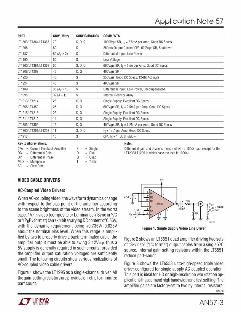
Figure 1. Single Supply Video Line Driver
Key to Abbreviations:CFA = Current Feedback Amplifi erDG = Differential GainDP = Differential PhaseMUX = MultiplexerSR = Slew Rate
Note:Differential gain and phase is measured with a 150Ω load, except for the LT1203/LT1205 in which case the load is 1000Ω.
S = SingleD = DualQ = QuadT = Triple
PART GBW (MHz) CONFIGURATION COMMENTS
LT1363/LT1364/LT1365 70 S, D, Q 1000V/µs SR, IS = 7.5mA per Amp, Good DC Specs
LT1206 60 S 250mA Output Current CFA, 600V/µs SR, Shutdown
LT1187 50 (AV ≥ 2) S Differential Input, Low Power
LT1190 50 S Low Voltage
LT1360/LT1361/LT1362 50 S, D, Q 600V/µs SR, IS = 5mA per Amp, Good DC Specs
LT1208/LT1209 45 D, Q 400V/µs SR
LT1220 45 S 250V/µs, Good DC Specs, 12-Bit Accurate
LT1224 45 S 400V/µs SR
LT1189 35 (AV ≥ 10) S Differential Input, Low Power, Decompensated
LT1995 32 (A = 1) S Internal Resistor Array
LT1213/LT1214 28 D, Q Single Supply, Excellent DC Specs
LT1358/LT1359 25 D, Q 600V/µs SR, IS = 2.5mA per Amp, Good DC Specs
LT1215/LT1216 23 D, Q Single Supply, Excellent DC Specs
LT1211/LT1212 14 D, Q Single Supply, Excellent DC Specs
LT1355/LT1356 12 D, Q 400V/µs SR, IS = 1.25mA per Amp, Good DC Specs
LT1200/LT1201/LT1202 11 S, D, Q IS = 1mA per Amp, Good DC Specs
LT1217 10 S CFA, IS = 1mA, Shutdown
VIDEO CABLE DRIVERS
AC-Coupled Video Drivers
When AC-coupling video, the waveform dynamics change with respect to the bias point of the amplifi er according to the scene brightness of the video stream. In the worst case, 1VP-P video (composite or Luminance + Sync in Y/C or YPBPR format) can exhibit a varying DC content of 0.56V, with the dynamic requirement being +0.735V/–0.825V about the nominal bias level. When this range is ampli-fi ed by two to properly drive a back-terminated cable, the amplifi er output must be able to swing 3.12VP-P, thus a 5V supply is generally required in such circuits, provided the amplifi er output saturation voltages are suffi ciently small. The following circuits show various realizations of AC-coupled video cable drivers.
Figure 1 shows the LT1995 as a single-channel driver. All the gain-setting resistors are provided on-chip to minimize part count.
Figure 2 shows an LT6551 quad amplifi er driving two sets of “S-video” (Y/C format) output cables from a single Y/C source. Internal gain-setting resistors within the LT6551 reduce part-count.
Figure 3 shows the LT6553 ultra-high-speed triple video driver confi gured for single-supply AC-coupled operation. This part is ideal for HD or high-resolution workstation ap-plications that demand high bandwidth and fast settling. The amplifi er gains are factory-set to two by internal resistors.

Application Note 57
AN57-4
an57fa
+
–OA
450Ω 450Ω
+
–OA
450Ω 450Ω
+
–OA
450Ω 450Ω
AN57 F02
+
–OA
450Ω 450Ω
1
2
3
4
5
10
9
8
7
6
75Ω 1k
4k470µF
75Ω
75Ω
1k
4k470µF
VCC = 5V
VCC = 5VLUMINANCE
CHROMA
75Ω
75Ω
75Ω
OUT2
OUT1
S-VIDEOCONNECTOR
S-VIDEOCONNECTOR
LUMINANCEOUT1
LUMINANCEOUT2
CHROMAOUT1
CHROMAOUT2
LT6551
+
7V TO 12V
80.6Ω
75Ω
75Ω
1/3 LT6553OUTIN
6.8k22µF* 220µF**INPUT
2.2k
AN57 F03
***
AVX 12066D226MATSANYO 6TPB220ML
AGND
Figure 2. S-Video Splitter
Figure 3. Single Supply Confi guration, One Channel Shown
DC-Coupled Video Drivers
The following circuits show various DC-coupled video drivers. In DC-coupled systems, the video swings are fi xed in relation to the supplies used, so back-terminated cable-drivers need only provide 2V of output range when optimally biased. In most cases, this permits operation on lower power supply potential(s) than with AC-coupling (unclamped mode). Generally DC-coupled circuits use split supply potentials since the waveforms often include or pass through zero volts. For single supply operation, the inputs need to have an appropriate offset applied to preserve linear amplifi er operation over the intended signal swing.
For systems that lack an available negative supply, the LT1983-3 circuit shown in Figure 5 can be used to easily produce a local-use –3V that can simplify an overall cable-driving solu-tion, eliminating large output electrolytics, for example.
Figure 6 shows a typical 3-channel video cable driver using an LT6553. This part includes on-chip gain-setting resis-tors and fl ow-through layout that is optimal for HD and RGB wideband video applications. This circuit is a good
The LT6557 400MHz triple video driver is specifi cally de-signed to operate in 5V single supply AC-coupled applications as shown in Figure 4. The input biasing circuitry is contained on-chip for minimal external component count. A single resistor programs the biasing level of all three channels.
VIN
SHDN
C +
VOUT
GND
C –
LTC1983-3
VIN3V TO 5.5V
VOUT = –3VIOUT = UP TO 100mA
COUT10µF
CIN10µF
CFLY1µF
OFF ON
CFLY: TAIYO YUDEN LMK212BJ105CIN, COUT: TAIYO YUDEN JMK316BJ106ML
AN57 F05
152
5V161
–3V–5V
–
+ 14
370Ω 370Ω75Ω
+
– 12
370Ω 370Ω
75Ω
+
– 10
9
5V11
–3V13
8
7
6
5
4
3
370Ω370Ω
75Ω
RIN
GIN
BIN
75Ω
75Ω
75Ω
75Ω
75Ω
75Ω
LT6553
AN57 F06
Figure 5. –3V at 100mA DC/DC Converter
Figure 6. Triple Video Line Driver
+–
500Ω
IN R
GND
EN
IN R OUT R
V+
V+ R
V+ G
V+ B
BCVLT6557
GND R75Ω 75Ω
412Ω5V
5V
5V
5VAN57 F04
10µF
500Ω
75Ω220µF
+–
500Ω
IN GIN G OUT G
GND G75Ω 75Ω
10µF
500Ω
75Ω220µF
+–
500Ω
IN BIN B OUT B
GND B75Ω 75Ω
10µF
500Ω
75Ω220µF
Figure 4. 400MHz, AC-Coupled, 5V Single Supply Video Driver

Application Note 57
AN57-5
an57fa
candidate for the LT1983-3 power solution in systems that have only 5V available.
Figure 7 shows the LT6551 driving four cables and op-erating from just 3.3V. The inputs need to have signals centered at 0.83V for best linearity. This application would be typical of standard-defi nition studio-environment signal distribution equipment (RGBS format).
Figure 8 shows a simple video splitter application using an LT6206. Both amplifi ers are driven by the input signal and each is confi gured for a gain of two, one for driving each
output cable. Here again careful input biasing is required (or a negative supply as suggested previously).
Figure 9 shows a means of providing a multidrop tap am-plifi er using the differential input LT6552. This circuit taps the cable (loop-through confi guration) at a high impedance and then amplifi es the signal for transmission to a stan-dard 75Ω video load (a display monitor for example). The looped-through signal would continue on to other locations before being terminated. The exceptional common mode rejection of the LT6552 removes any stray noise pickup on the distribution cable from corrupting the locally displayed video. This method is also useful for decoupling of ground-loop noise between equipment, such as in automotive entertainment equipment. To operate on a single supply, the input signals shown (shield and center of coax feed) should be non-negative, otherwise a small negative supply will be needed, such as the local –3V described earlier.
Figure 7. 3.3V Single Supply LT6551 RGB Plus SYNC Cable Driver
+
–
ROUT
3.3V
OA
450Ω 450Ω
75Ω
+
–
GOUT
OA
450Ω 450Ω
75Ω
+
–
BOUT
OA
450Ω 450Ω
75Ω
+
–
SYNCOUT
RIN
GIN
BIN
SYNCIN
GND
OA
450Ω 450Ω
75Ω
75Ω
75Ω
75Ω
75Ω
75Ω
75Ω
75Ω
75Ω
LT6551
AN57 F07
Figure 8. Baseband Video Splitter/Cable Driver
–
+
–
+
LT6206
VIN
1µF 75Ω
75Ω
75Ω
75Ω
75Ω
VOUT1
VOUT2
3.3V
499Ω 499Ω
499Ω 499Ω
1
7
4
8
6
5
3
2
F3dB ≈ 50MHzIS ≤ 25mA
AN57 F08
Figure 9. Cable Sense Amplifi er for Loop Through Connections with DC Adjust
7
6LT6552
4
18
VOUT
+3
–REFFB
2
VIN
RF500Ω
VDC
RG500Ω
5V
75Ω
75Ω
CABLE
AN57 F09
CF8pF
Clamped AC-Input Video Cable Driver
The circuit in Figure 10 shows a means of driving composite video on standard 75Ω cable with just a single 3.3V power supply. This is possible due to the low output saturation levels of the LT6205 and the use of input clamping to optimize the bias point of the amplifi er for standard 1VP-P source video. The circuit provides an active gain of two and 75Ω series termination, thus yielding a net gain of one as seen by the destination load (e.g. display device). Additional detail on this circuit and other low-voltage considerations can be found in Design Note 327.
Twisted-Pair Video Cable Driver and Receiver
With the proliferation of twisted-pair wiring practices for in-building data communication, video transmission on the

Application Note 57
AN57-6
an57fa
same medium offers substantial cost savings compared to conventional coaxial-cable. Launching a baseband camera signal into twisted pair is a relatively simple matter of building a differential driver such as shown in Figure 11. In this realization one LT6652 is used to create a gain of +1 and another is used to make a gain of –1. Each output is series terminated in half the line impedance to provide a balanced drive condition. An additional virtue of using the LT6552 in this application is that the incoming unbalanced signal (from a camera for example) is sensed differentially, thereby rejecting any ground noise and preventing ground loops via the coax shield.
At the receiving end of the cable, the signal is terminated and re-amplifi ed to re-create an unbalanced output for
connection to display monitors, recorders, etc. The ampli-fi er not only has to provide the 2x gain required for the output drive, but must also make up for the losses in the cable run. Twisted pair exhibits a rolloff characteristic that requires equalization to correct for, so the circuit in Figure 12 shows a suitable feedback network that accomplishes this. Here again the outstanding common mode rejection of the LT6552 is harnessed to eliminate stray pickup that occurs in long cable runs.
–
+LT6205
COMPOSITEVIDEO IN 1VP–P
0.1µF
C14.7µF
C24.7µF
BAT54
75Ω
10k
75Ω
VIDEO OUT
3.3V
1k 1k
2.4k
1
2
5
3
4
IS ≤ 19mA
AN57 F10
470Ω
Figure 10. Clamped AC-Input Video Cable Driver
+–
1k
FB
REF
8
1
2
3
LT6552SD
TP+
TWISTED PAIRZ0 ≈ 110Ω
5V
–5V
54.9Ω
75Ω
CAMERA VIDEOINPUT
75Ω
6
57
4
+–
FB
REF
8
1
2
3
LT6552SD
TP–
5V
–5V
54.9Ω
AN57 F11
6
57
4
Figure 11. Super-Simple Coax to Twisted-Pair Adapter
+–
220pF
150pF
768Ω
110Ω
2.34k
68pF909Ω
10k
1k
1k
100Ω
FB
REFLT6552
SD
10k 10k
TP+
TP–
1VP–PBALANCED
S1S2
5V
–5V
75Ω VIDEO OUTPUT1VP–P75Ω
EQUALIZATION
S1 OPEN, S2 OPEN: NO EQUALIZATIONS1 CLOSED, S2 OPEN: EQUALIZATION FOR ≈ 300ftS1 OPEN, S2 CLOSED: EQUALIZATION FOR ≈ 700ftS1 CLOSED, S2 CLOSED: EQUALIZATION FOR ≈ 1000ft
8
1
2
3
6
57
4
AN57 F12
Figure 12. All-In-One Twisted-Pair Video Line Receiver, Cable Equalizer, and Display Driver
VIDEO PROCESSING CIRCUITS
ADC Driver
Figure 13 shows the LT6554 triple video buffer. This is a typical circuit used in the digitization of video within high resolution display units. The input signals (terminations not shown) are buffered to present low source impedance and fast settling behavior to ADC inputs that is generally required to preserve conversion linearity to 10 bits or better. With high resolution ADCs, it is typical that the settling-time requirement (if not distortion performance) will call for buffer bandwidth that far outstrips the baseband signals themselves in order to preserve the effective number of [conversion] bits (ENOBs). The 1kΩ loads shown are simply to represent the ADC input for characterization purposes, they are not needed in the actual use of the part.

Application Note 57
AN57-7
an57fa
Video Fader
In some cases it is desirable to adjust amplitude of a video waveform, or cross-fade between two different video sources. The circuit in Figure 14 provides a simple means of accomplishing this. The 0V to 2.5V control voltage provides a steering command to a pair of amplifi er input sections; at each extreme, one section or the other takes complete control of the output. For intermediate control voltages, the inputs each contribute to the output with a weighting that follows a linear function of control voltage (e.g. at VCONTROL = 1.25V, both inputs contribute at 50%). The feedback network to each input sets the maximum gain in the control range (unity gain is depicted in the example), but depending on the application, other gains or even equalization functions can be voltage controlled
(see datasheet and Application Note 67 for additional examples). In the fader example below, it should be noted that both input streams must be gen-locked for proper operation, including a black signal (with sync) if fading to black is intended.
Color Matrix Conversion
Depending on the conventions used by video suppliers in products targeting specifi c markets, various standards for color signaling have evolved. Television studios have long used RGB cameras and monitor equipment to maximize signal fi delity through the equipment chain. With computer displays requiring maximum performance to provide clear text and graphics, the VESA standards also specify an RGB format, but with separate H and V syncs sent as logic signals. Video storage and transmission systems, on the other hand, seek to minimize information content to the extent that perceptual characteristics of the eye limit any apparent degradation. This has led to utilizing color-differencing approaches that allowed reducing bandwidth on the color information channels without noticeable loss in image sharpness. The consumer 3-chan-nel “component” video connection (YPBPR) has a luma + sync (Y) plus blue and red axis color-space signals (PB and PR, respectively) that are defi ned as a matrix multiplication applied to RGB raw video. The color difference signals are typically half the spatial resolution of the luma according to the compression standards defi ned for DVD playback and digitally broadcast source material, thus lowering “band-width” requirements by some 50%. The following circuits show methods of performing color-space mappings at the physical layer (analog domain).
Figure 15 shows a method of generating the standard-defi -nition YPBPR signals from an RGB source using a pair of LT6550 triple amplifi ers. It should be noted that to ensure Y includes a correct sync, correct syncs should be present at all three inputs or else added directly at the Y output (gated 8.5mA current sink or 350Ω switched to –3.3V). This circuit does not deliberately reduce bandwidth on the color component outputs, but most display devices will nonetheless apply a Nyquist fi lter at the digitizer section of the “optical engine” in the display unit. The circuit is shown as DC-coupled, so ideally black level is near ground for best operation with the low-voltage supplies shown. Adding input coupling capacitors will allow processing source video that has substantial offset.
An LT6559 and an LT1395 can also be used to map RGB
152
5V161
–5V–5V
–
+ 14
480Ω
+
– 12
480Ω
+
– 10
9
5V11
–5V13
8
7
6
5
4
3
480Ω
RIN
GIN
BIN
1k
1k
1k
LT6554
AN57 F13
Figure 13. Triple Video Buffer and A/D Driver
–
+
–
+
IN1 IN2
2.5VDCINPUT
RF21.5k
VOUT
RF11.5k
IFS
IC
IC
V+
V–
NULL
AN57 F14
0V TO 2.5VCONTROL
2–
+
–
+
1
2
3
4
5
6
7
14
13
12
11
10
9
8
CONTROL
LT1251/LT1256
1
C FS
5k5k
IFS
Figure 14. Two-Input Video Fader
Application Note 57
AN57-8
an57fa
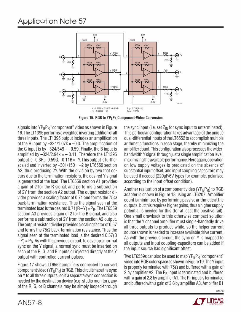
signals into YPBPR “component” video as shown in Figure 16. The LT1395 performs a weighted inverting addition of all three inputs. The LT1395 output includes an amplifi cation of the R input by –324/1.07k = –0.3. The amplifi cation of the G input is by –324/549 = –0.59. Finally, the B input is amplifi ed by –324/2.94k = – 0.11. Therefore the LT1395 output is –0.3R, –0.59G, –0.11B = –Y. This output is further scaled and inverted by –301/150 = –2 by LT6559 section A2, thus producing 2Y. With the division by two that oc-curs due to the termination resistors, the desired Y signal is generated at the load. The LT6559 section A1 provides a gain of 2 for the R signal, and performs a subtraction of 2Y from the section A2 output. The output resistor di-vider provides a scaling factor of 0.71 and forms the 75Ω back-termination resistance. Thus the signal seen at the terminated load is the desired 0.71(R – Y) = PR. The LT6559 section A3 provides a gain of 2 for the B signal, and also performs a subtraction of 2Y from the section A2 output. The output resistor divider provides a scaling factor of 0.57 and forms the 75Ω back-termination resistance. Thus the signal seen at the terminated load is the desired 0.57(B – Y) = PB. As with the previous circuit, to develop a normal sync on the Y signal, a normal sync must be inserted on each of the R, G, and B inputs or injected directly at the Y output with controlled current pulses.
Figure 17 shows LT6552 amplifi ers connected to convert component video (YPBPR) to RGB. This circuit maps the sync on Y to all three outputs, so if a separate sync connection is needed by the destination device (e.g. studio monitor), any of the R, G, or B channels may be simply looped-through
the sync input (i.e. set ZIN for sync input to unterminated). This particular confi guration takes advantage of the unique dual-differential inputs of the LT6552 to accomplish multiple arithmetic functions in each stage, thereby minimizing the amplifi er count. This confi guration also processes the wider-bandwidth Y signal through just a single amplifi cation level, maximizing the available performance. Here again, operation on low supply voltages is predicated on the absence of substantial input offset, and input coupling capacitors may be used if needed (220µF/6V types for example, polarized according to the input offset condition).
Another realization of a component video (YPBPR) to RGB adapter is shown in Figure 18 using an LT6207. Amplifi er count is minimized by performing passive arithmetic at the outputs, but this requires higher gains, thus a higher supply potential is needed for this (for at least the positive rail). One small drawback to this otherwise compact solution is that the Y channel amplifi er must single-handedly drive all three outputs to produce white, so the helper current source shown is needed to increase available drive current. As with the previous circuit, the sync on Y is mapped to all outputs and input coupling-capacitors can be added if the input source has signifi cant offset.
Two LT6559s can also be used to map YPBPR “component” video into RGB color space as shown in Figure 19. The Y input is properly terminated with 75Ω and buffered with a gain of 2 by amplifi er A2. The PR input is terminated and buffered with a gain of 2.8 by amplifi er A1. The PB input is terminated and buffered with a gain of 3.6 by amplifi er A3. Amplifi er B1
+
–
450Ω 450Ω
+
–
450Ω 450Ω
+
–
450Ω 450Ω
1R
G
B
PR
Y
PB
2
3
4 5
9
10
8
7
1070Ω
549Ω
2940Ω
75Ω
75Ω
174Ω
LT6550
261Ω
75Ω
–3.3V
3.3V 3.3V
+
–
450Ω 450Ω
+
–
450Ω 450Ω
+
–
450Ω 450Ω
1
2
3
4 5
9
10
8
7
105Ω
75Ω
133Ω
LT6550
–3.3VAN57 F15
Y = 0.299R + 0.587G + 0.114BPB = 0.565(B – Y)
PR = 0.713(R – Y) f3dB ≈ 44MHz
Figure 15. RGB to YPBPR Component-Video Conversion
Application Note 57
AN57-9
an57fa
–+
FB
REFLT6552
–3V
SD
+3V499Ω499Ω
5.6pF
75Ω
75Ω
8
1
2
34
5
6
7
–+
FB
REFLT6552
–3V
SD
+3V499Ω499Ω
8.2pF
8
1
2
34
5
6
7G
–+
FB
REFLT6552
–3V
SD
+3V909Ω499Ω
2.2pF
75Ω
75Ω
8
1
2
34
5
6
7
R
–+
FB
REFLT6552
–3V
SD
+3V1.3k499Ω
1pF
75Ω
75Ω
8
1
2
34
5
6
7
B
21.5Ω21.5Ω
53.6Ω
49.9Ω
25.5Ω
11.3Ω
42.2Ω
PR
PB
R = Y + 1.4 • PRG = Y – 0.34 • PB – 0.71 • PRB = Y + 1.8 • PB
BW (± 0.5dB) > 25MHzBW (–3dB) > 36MHzIS ≈ 70mA AN57 F17
Y
Figure 17. YPBPR to RGB Video Converter
Figure 16. High Speed RGB to YPBPR Converter
75Ω
PB
Y
133Ω
PR
105Ω
–
+A2
LT1395–
+A2
1/3 LT6559
–
+A1
1/3 LT6559
324Ω
150Ω 301Ω
2940Ω
549Ω
80.6Ω
174Ω
261ΩR
G
B
86.6Ω
76.8Ω
ALL RESISTORS 1%VS = ±3V TO ±5V
Y = 0.3R + 0.59G + 0.11BPB = 0.57(B – Y)PR = 0.71(R – Y)
1070Ω
75ΩSOURCES
301Ω
301Ω
301Ω
301Ω
AN57 F16
–
+A3
1/3 LT6559
performs an equally weighted addition of amplifi ers A1 and A2 outputs, thereby producing 2(Y + 1.4PR), which gener-ates the desired R signal at the terminated load due to the voltage division by 2 caused by the termination resistors. Amplifi er B3 forms the equally weighted addition of ampli-fi ers A1 and A3 outputs, thereby producing 2(Y + 1.8PB),
which generates the desired B signal at the terminated load. Amplifi er B2 performs a weighted summation of all three inputs. The PB signal is amplifi ed overall by –301/1.54k • 3.6 = 2(–0.34). The PR signal is amplifi ed overall by –301/590 • 2.8 = 2(–0.71). The Y signal is amplifi ed overall by 1k/(1k + 698) • (1 + [301/(590||1.54k)]) • 2 = 2(1). Therefore

Application Note 57
AN57-10
an57fa
Figure 18. YPBPR to RGB Converter
150Ω
499Ω
150Ω
150Ω
150Ω
107Ω
80.6Ω
499Ω
75Ω
75Ω
R
B
150Ω
150Ω
75Ω
G
F3dB ≈ 40MHzIS ≤ 60mABLACK LEVELS ≈ 0V
R = Y + 1.4 • PR B = Y + 1.8 • PBG = Y – 0.34 • PB – 0.71 • PR AN57 F18
LT6207
14
16
15
12
11
10
13
4
6
7
5
3
2
1
1µF
133Ω
75Ω
36Ω
FMMT3906
CMPD6001S
4.7k
95.3Ω174Ω
5V
1µF–5V
499Ω365Ω
499Ω165Ω
PR
PB
Y
–
+
–
+
–
+
–
+
the amplifi er B2 output is 2(Y – 0.34PB – 0.71PR), which generates the desired G signal at the terminated load. Like the previous circuits shown, sync present on the Y input is reconstructed on all three R, G, and B outputs.
Video Inversion
The circuit in Figure 20 is useful for viewing photographic negatives on video. A single channel can be used for com-posite or monochrome video. The inverting amplifi er stages
are only switched in during active video so the blanking, sync and color burst (if present) are not disturbed. To prevent video from swinging negative, a voltage offset equal to the peak video signal is added to the inverted signal.
Graphics Overlay Adder
Multiplexers that provide pixel-speed switching are also useful in providing simple graphics overlay, such as time-stamps or logo “bugs”. Figure 21 shows an LT1675 pair
Figure 19. High Speed YPBPR to RGB Converter
PR
PB
+
–B1
1/3 LT6559 R75Ω
1k
1k
301Ω
V+
V–
301Ω
+
–A1
1/3 LT6559
301Ω
V+
V–
165Ω
75Ω+
–A3
1/3 LT6559
301Ω
V+
V–
118Ω
Y
75Ω
75Ω
+
–A2
1/3 LT6559
301Ω
V+
V–
301Ω
+
–B2
1/3 LT6559 G75Ω
1k
698Ω
301Ω
V+
V–
590Ω
1.54k
+
–B3
1/3 LT6559
55
5
5 5
5
B75Ω
1k
1k
324Ω
V+
V–
324Ω
AN57 F19
R = Y + 1.4 • PRG = Y – 0.34 • PB – 0.71 • PR B = Y + 1.77 • PB
V+/V– = ±3V

Application Note 57
AN57-11
an57fa
RED
VIDEO IN GREEN
BLUE
75Ω
75Ω
75Ω
75Ω
CABLE
CABLE
CABLE
V+
V–
SELECT
AN57 F20
ENABLE
COMPOSITEBLANKING
97.6Ω
97.6Ω
97.6Ω
VOUT RED
75Ω
LT1675
75Ω
VOUT GREEN
VOUT BLUE
+1
+1+2
+2
+2
+1
+1
+1
+1
332Ω 332Ω
+
–
332Ω 332Ω
+
–
332Ω
10k
10k
LT1634
LT1399
5V
0.714V
1.25V
332Ω
+
–
Figure 20. RGB Video Inverter
RED
VIDEO IN GREEN
BLUE
113Ω
75Ω
75Ω
75Ω
CABLE
CABLE
CABLE
V+
V–
SELECT
SELECT A
SELECT B
AN57 F21
ENABLE
75Ω
75Ω
75Ω
VOUT RED
113Ω
LT1675
113Ω
VOUT GREEN
VOUT BLUE
+1
+1+2
+2
+2
+1
+1
+1
+1
226Ω
V+
V–
SELECT
ENABLE
226Ω
LT1675
B
A
226Ω
+1
+1+2
+2
+2
+1
+1
+1
+110k
10k
LT1634
5V
0.714V
1.25V
SELECT A0011
SELECT B0101
OUTPUTNO VIDEO, 100% WHITEVIDEO PLUS 66% WHITEVIDEO PLUS 33% WHITEVIDEO, NO WHITE
Figure 21. Logo or “Bug” Inserter

Application Note 57
AN57-12
an57fa
used to insert multilevel overlay content from a digital generator. The instantaneous state of the two input control lines selects video or white in each device and combines their outputs with the resistor-weighted summing networks at the output. With the four combinations of control line states, video, white, and two differing brightening levels are available.
Variable Gain Amplifi er Has ±3dB Range While Maintaining Good Differential Gain and Phase
The circuit in Figure 22 is a variable gain amp suitable for composite video use. Feedback around the transcon-duct-ance amp (LT1228) acts to reduce the differential input voltage at the amplifi er’s input, and this reduces the differential gain and phase errors. Table 1 shows the differential phase and gain for three gains. Signal-to-noise ratio is better than 60dB for all gains.
Table 1.INPUT
(V)ISET (mA)
DIFFERENTIAL GAIN
DIFFERENTIAL PHASE
0.707 4.05 0.4% 0.15°
1.0 1.51 0.4% 0.1°
1.414 0.81 0.7% 0.5°
Black Clamp
Here is a circuit that removes the sync component of the video signal with minimal disturbance to the luminance
(picture information) component. It is based on the clas-sic op amp half-wave-rectifi er with the addition of a few refi nements.
The classic “diode-in-the-feedback-loop” half-wave-rectifi er circuit generally does not work well with video frequency signals. As the input signal swings through zero volts, one of the diodes turns on while the other is turned off, hence the op amp must slew through two diode drops. During this time the amplifi er is in slew limit and the output signal is distorted. It is not possible to entirely prevent this source of error because there will always be some time when the amp will be open-loop (slewing) as the diodes are switched, but the circuit shown here in Figure 23 minimizes the error by careful design.
The following techniques are critical in the design shown in Figure 23:
1. The use of diodes with a low forward voltage drop reduces the voltage that the amp must slew.
2. Diodes with a low junction capacitance reduce the ca-pacitive load on the op amp. Schottky diodes are a good choice here as they have both low forward voltage and low junction capacitance.
3. A fast slewing op amp with good output drive is es-sential. An excellent CFA like the LT1227 is mandatory for good results.
4. Take some gain. The error contribution of the diode switch tends to be constant, so a larger signal means a smaller percentage error.
Figure 22. ±3dB Variable Gain Video Amp Optimized for Differential Gain and Phase
–
+–
+
750Ω250Ω
75Ω 3.4k
CFA(LT1228)
681Ω
–
+
2k75Ω75Ω
1.5k
1k
750Ω
75ΩOUT
IN
ISET
750Ω
AN57 F22
gm(LT1228)
VS = ±15VVOUT = 1VP-PS/N MEASURES > 60dB
LT1227

Application Note 57
AN57-13
an57fa
Since this circuit discriminates between the sync and video on the basis of polarity, it is necessary to have an input video signal that has been DC restored (the average DC level is automatically adjusted to bring the blanking level to zero volts). Notice that not only is the positive polarity information (luminance: point A in the schematic) available, but that the negative polarity information (sync: point B in the schematic) is also. Circuits that perform this function are called “black clamps.” The photograph (Figure 24) shows the circuit’s clean response to a 1T1 pulse (some extra delay is added between the input and output for clarity).
Video Limiter
Often there is a need to limit the amplitude excursions of the video signal. This is done to avoid exceeding luminance reference levels of the video standard being used, or to avoid exceeding the input range of another processing stage such as an A/D converter. The signal can be hard limited in the positive direction, a process called “white peak clipping,” but this destroys any amplitude information and hence any scene detail in this region. A more gradual limiting (“soft limiter”) or compression of the peak white excursion is performed by elements called “knee” circuits, after the shape of the amplifi er transfer curve.
A soft limiter circuit is shown in Figure 25 which uses the LT1228 transconductance amp. The level at which the limiting action begins is adjusted by varying the set current into pin 5 of the transconductance amplifi er. The LT1228 is used here in a slightly unusual, closed-loop confi guration. The closed-loop gain is set by the feedback and gain resistors (RF and RG) and the open-loop gain by the transconductance of the fi rst stage times the gain of the CFA.
–
+
750Ω75ΩIN
75ΩOUT
750Ω
LT1227
–
+LT1227
750Ω2k
75Ω
0VB
A
AN57 F23
1N5712
1N5712
Figure 23. Black Clamp Circuit
Figure 24. Black Clamp Circuit Response to a “1T” Pulse (±15V Power Supplies)
1 A 1T pulse is a specialized video waveform whose salient characteristic is a carefully controlled bandwidth which is used to quickly quantify gain and phase fl atness in video systems. Phase shift and/or gain variations in the video system’s passband result in transient distortions which are very noticeable on this waveform (not to mention the picture). [For you video experts out there, the K factor was 0.4% (the TEK TSG120 video signal generator has a K factor of 0.3%)].
AN57 F24
Application Note 57
AN57-14
an57fa
As the transconductance is reduced (by reducing the set current), the open-loop gain is reduced below that which can support the closed-loop gain and the amp limits. A family of curves which show the response of the limiting amplifi er subject to different values of set current with a ramp input is shown in Figure 26. Figure 27 shows the change in limiting level as ISET is varied.
Circuit for Gamma Correction
Video systems use transducers to convert light to an electric signal. This conversion occurs, for example, when a camera scans an image. Video systems also use transducers to
convert the video signal back to light when the signal is sent to a display, a CRT monitor for example. Transducers often have a transfer function (the ratio of signal in to light out) that is unacceptably nonlinear.
The newer generation of camera transducers (CCDs and the improved versions of vidicon-like tubes) are adequately linear, however, picture monitor CRTs are not. The transfer functions of most CRTs follow a power law. The following equation shows this relation:
Light Out = k • VSIGγ
where k is a constant of proportionality and gamma (γ) is the exponent of the power law (gamma ranges from 2.0 to 2.4).
This deviation from nonlinearity is usually called just gamma and is reported as the exponent of the power law. For instance, “the gamma of this vidicon is 0.43.” The correction of this effect is gamma correction.
In the equation above, notice that a gamma value of 1 results in a linear transfer function. The typical CRT will have a transfer function with a gamma from about 2.0 to 2.4. Such values of gamma give a nonlinear response which compresses the blacks and stretches the whites. Cameras usually contain a circuit to correct this nonlin-earity. Such a circuit is a gamma corrector or simply a gamma circuit.
Figure 25. LT1228 Soft Limiter
Figure 26. Output of the Limiting Amp (ISET = 0.68mA), with a Ramp Input. As the Input Amplitude Increases from 0.25V to 1V, the Output is Limited to 1V
Figure 27. The Output of the Limiting Amp with Various Limiting Levels (ISET). The Input is a Ramp with a Maximum Amplitude of 0.75V
–
+–
+
750Ω250Ω
75Ω 3.4k
CFA(LT1228)
681Ω2k75Ω
6 75ΩOUT
ISET
AN57 F25
gm(LT1228)
8
1
2
3
INPU
T (V
)
AN57 F26
0
1.0
1.0
OUTP
UT (V
)
0
AN57 F27
ISET (mA)
2.7
1.9
1.4
1.0
0.68
0.35VERT
ICAL
: 0.5
V/DI
V

Application Note 57
AN57-15
an57fa
AN57 F30
Figure 28 shows a schematic of a typical circuit which can correct for positive or negative gamma. This is an upgrade of a classic circuit which uses diodes as the nonlinear elements. The temperature variation of the diode junction voltages is compensated to the fi rst order by the balanced arrangement. LT1227s and LT1229s were used in the prototype, but a quad (LT1230) could save some space and work as well.
Figure 29, curve A, shows a response curve (transfer func-tion) for an uncorrected CRT. To make such a response linear, the gamma corrector must have a gamma that is the reciprocal of the gamma of the device being linearized. The response of a two diode gamma circuit like that in Figure 28 is shown in Figure 29, curve B. Summing these two curves together, as in Figure 29, curve C, demonstrates the action of the gamma corrector. A straight line of ap-propriate slope, which would be an ideal response, is shown for comparison in Figure 29, curve D. Figure 30 is a triple exposure photograph of the gamma corrector circuit adjusted for gammas of –3, 1 and +3 (approximately). The input is a linear ramp of duration 52µs which is the period of an active horizontal line in NTSC video.
Figure 30. Gamma Corrector Circuit Adjusted for Three Gammas: –3, 1, +3 (Approximately). The Input is a Linear Ramp
Figure 28. Gamma Amp (Input Video Should Be Clamped)
Figure 29. Uncorrected CRT Transfer Function
–
+
–
+
1k
10k
LT1229
100Ω
–
+
2k
75Ω
1k150Ω
OUT
AN57 F28
LT1227A
150Ω
1k
–
+1N4148
1N4148
1N4148
1N4148
1k
1k
RESPONSE AT POINT A
RESPONSE AT POINT B75Ω
LT1229
LT1227
B
0
LIGHTOUT
(RELATIVESCALE)
1.0
1.5
0.5
01.0 2.0 3.00.5 1.5 2.5
“C”(A + B)
“D”IDEAL
B
AUNCORRECTED
AN57 F29INPUT SIGNAL LEVEL (V)
Application Note 57
AN57-16
an57fa
LT1228 Sync Summer
The circuit shown in Figure 31a restores the DC level and adds sync to a video waveform. For this example the video source is a high speed DAC with an output which is refer-enced to –1.2V. The LT1228 circuit (see the LT1228 data sheet for more details) forms a DC restore2 that maintains a zero volt DC reference for the video. Figure 31b shows the waveform from the DAC, the DC restore pulse, and composite sync. The LT1363 circuit sums the video and composite sync signals. The 74AC04 CMOS inverters are used to buffer the TTL composite sync signal. In addition they drive the shaping network and, as they are mounted on the same ground plane as the analog circuitry, they isolate the ground noise from the digital system used to generate the video timing signals. Since the sync is directly summed to the video, any ground bounce or noise gets added in too. The shaping network is simply a third order Bessel lowpass fi lter with a bandwidth of 5MHz and an impedance of 300Ω. This circuitry slows the edge rate of the digital composite sync signal and also attenuates the noise. The same network, rescaled to an impedance of 75Ω,
is used on the output of the summing amp to attenuate the switching noise from the DAC and to remove some of the high frequency components of the waveform. A more selective fi lter is not used here as the DAC has low glitch energy to start with and the signal does not have to meet stringent bandwidth requirements. The LT1363 used for the summing amp has excellent transient characteristics with no overshoot or ringing. Figure 31c shows two horizontal
Figure 31a. Simple Sync Summer
2 This is also referred to as “DC clamp” (or just clamp) but, there is a distinction. Both clamps and DC restore circuits act to maintain the proper DC level in a video signal by forcing the blanking level to be either zero volts or some other appropriate value. This is necessary because the video signal is often AC coupled as in a tape recorder or a transmitter. The DC level of an AC coupled video signal will vary with scene content and therefore the black referenced level must be “restored” in order for the picture to look right. A clamp is differentiated from a DC restore by its speed of response. A clamp is faster, generally correcting the DC error in one horizontal line (63.5µs for NTSC). A DC restore responds slower, more on the order of the frame time (16.7ms for NTSC). If there is any noise on the video signal the DC restore is the preferred method. A clamp can respond to noise pulses that occur during the blanking period and as a result give an erroneous black level for the line. Enough noise causes the picture to have an objectionable distortion called “piano keying.” The black reference level and hence the luminance level change from line to line.
–
+
1000Ω LT1228200Ω
75Ω
75Ω75Ω
2.2k5k
510Ω
510Ω300Ω
74AC04
300Ω232pF36.5pF
421 39.3µH
75Ω
75Ω10k
OUT
+V
V+
+V
–V
–
+
–
+
CFA
750Ω
1k
1k
1k
340Ω
0.01µF
935pF
143pF
LT1363
2.3µH
2N3906
200Ω
7
1
584
3
6
73
2
3
2
AN57 F31a
75Ω
gm
T2L LEVELS
T2L LEVELS
VIDEOFROMDAC
RESTORE
COMPOSITE SYNC

Application Note 57
AN57-17
an57fa
Figure 31b. Video Waveform from DAC; Clamp Pulse and Sync Pulse Used as Inputs to Sync Summer
Figure 31d. Close-Up of Figure 31c, Showing Sync Pulse
Figure 31c. Reconstructed Video Out of Sync Summer
lines of the output waveform with the DC restored and the sync added. Figure 31d is an expanded view of the banking interval showing a clean, well formed sync pulse.
MULTIPLEXER CIRCUITS
Integrated Three-Channel Output Multiplexer
The LT6555 is a complete 3-channel wideband video 2:1 multiplexer with internally set gain of two. This part is ideal as an output port driver for HD component or high-resolu-tion RGB video products. The basic application circuit is shown in Figure 32 with terminations shown on all ports, though in many applications the input loading may not be required. One thing this diagram does not refl ect is the convenient fl ow-through pin assignments of the part, in which no video traces need cross in the printed-circuit layout. This maximizes isolation between channels and sources for best picture quality.
Since the LT6555 includes an enable control line, it is possible to extend the selection range of the multiplexer. Figure 33 shows two LT6555 devices in a confi guration that provides 4:1 selection of RGB sources to an RGB output port (these could also be YPBPR signals as well, depending on the source). To avoid frequency response anomalies, the
LT6555
V+
V–
RINAGINABINA
RINBGINBBINB
75Ω
75Ω
75Ω
75Ω
75Ω
75ΩSELECT A/B
AN57 F32
AGND
ENABLE
DGND
75Ω75ΩROUT
75Ω75ΩGOUT
75Ω75ΩBOUT
×2
×2
×2
Figure 32. Multiplexer and Line Driver
AN57 F31c
AN57 F31c
AN57 F31b

Application Note 57
AN57-18
an57fa
two devices should be closely located so that the output lines between parts are as short as possible.
The LT1675 is also an integrated 3-channel 2:1 multiplexer that includes gain of two for cable-driving applications. The basic confi guration is shown in Figure 34. A single channel version for composite video applications is avail-able as an LT1675-1.
Integrated Three-Channel Input Multiplexer
The LT6556 is a complete 3-channel wideband video 2:1 multiplexer with internally set gain of one. This part is ideal as an input port receiver for HD component or high-resolu-tion RGB video products. The basic application circuit is shown in Figure 35, with 1kΩ output loads to represent subsequent processing circuitry (the 1kΩ resistors aren’t
needed, but part characterization was performed with that loading). One thing this diagram does not refl ect is the convenient fl ow-through pin assignments of the part, in which no video traces need cross in the printed-circuit layout. This maximizes isolation between channels and sources for best picture quality.
As with the LT6555, the LT6556 includes an enable control line, so it is possible to extend the selection range of this multiplexer as well. Figure 36 shows two LT6556 devices in a confi guration that provides 4:1 selection of RGB sources to an RGB signal processing function, such as a digitizer in a projection system (these could be YPBPR signals just as well). To avoid frequency response anomalies, the two devices should be closely located so that the output lines between parts are as short as possible.
Figure 33. 4:1 RGB Multiplexer
×2
LT6555 #1 V+
IN1A
RED 1GREEN 1
BLUE 1
RED 2GREEN 2
BLUE 2
75Ω
75Ω
IN1B
×2
IN2A75Ω
75Ω
75Ω
75Ω
75Ω
IN2B
×2
IN3A
IN3B
SEL
OUT3
OUT2
OUT1
–3V75Ω
GOUT
AGND
OUT1
OUT2
EN
5V
DGND
V–
VREF
×2
LT6555 #2 V+
IN1A
RED 3GREEN 3
BLUE 3
RED 4GREEN 4
BLUE 4
SEL0
SEL1
75Ω
75Ω
IN1B
×2
IN2A75Ω
75Ω
75Ω
75Ω
IN2B
×2
IN3A
IN3B
SEL
OUT3
–3V
AGND
EN
5V
DGND
AN57 F33
V–
VREF
75Ω
75ΩROUT
75Ω
75ΩBOUT
NC75Z14
SEL10011
SEL00101
OUTPUT1234
Application Note 57
AN57-19
an57fa
LT6556
V+
V–
RINAGINABINA
RINBGINBBINB
75Ω
75Ω
75Ω
75Ω
75Ω
75ΩVREF
AN57 F35
AGND
ENABLE
DGND
1kROUT
1kGOUT
1kBOUT
×1
×1
×1
SELECT A/B
Figure 34. 2:1 RGB Multiplexer and Cable Driver
RED 1
GREEN 1
BLUE 1
RED 2
GREEN 2
BLUE 2
75Ω
75Ω
75Ω
75Ω
CABLE
CABLE
CABLE
V+
V–
SELECT RGB1/RGB2
AN57 F34
ENABLE
75Ω
75Ω
75Ω
75Ω
75Ω
75Ω
VOUT RED
75Ω
LT1675
75Ω
VOUT GREEN
VOUT BLUE
+1
+1+2
+2
+2
+1
+1
+1
+1
Figure 35. Buffered Input Multiplexer/ADC Driver
Figure 36. 4:1 RGB Multiplexer
×1
LT6556 #1 V+
IN1A
RED 1GREEN 1
BLUE 1
RED 2GREEN 2
BLUE 2
75Ω
75Ω
IN1B
×1
IN2A75Ω
75Ω
75Ω
75Ω
IN2B
×1
IN3A
IN3B
SEL
OUT3
OUT2
OUT1
–3V GOUT
AGND
OUT1
OUT2
EN
5V
DGND
V–
VREF
×1
LT6556 #2 V+
IN1A
RED 3GREEN 3
BLUE 3
RED 4GREEN 4
BLUE 4
SEL0
SEL1
75Ω
75Ω
IN1B
×1
IN2A75Ω
75Ω
75Ω
75Ω
IN2B
×1
IN3A
IN3B
SEL
OUT3
–3V
AGND
EN
5V
DGND
AN57 F36
V–
VREF
ROUT
BOUT
NC7SZ14
SEL10011
SEL00101
OUTPUT1234

Application Note 57
AN57-20
an57fa
A 3:1 cable-driving multiplexer for composite video can be formed from a single LT1399 as shown in Figure 37. The LT1399 has the unusual feature of having independent enable controls for each of the three sections. The gain of the amplifi ers is set to compensate for passive loss in the loading associated with the off-section feedback networks.
Forming RGB Multiplexers From Triple Amplifi ers
The LT6553 triple cable driver and LT6554 triple buffer amp each provide an enable pin, so these parts can be used to implement video multiplexers. Figure 38 shows a pair of LT6553 devices confi gured as a 2:1 output multiplexer and cable driver. Similarly, Figure 39 shows a pair of LT6554 devices forming a 2:1 input mux, suitable as an ADC driver. These circuits are functionally similar to the LT6555 and LT6556 integrated multiplexers, but offer the fl exibility of providing the mux feature as a simple stuffi ng option to a single printed circuit design, possibly reducing production costs when multiple product grades are being concurrently manufactured. For best results the two devices should be closely located and use minimal trace lengths between them for the shared output signals.
–
+1/3 LT1399RG
200Ω
RF324Ω
A
EN AVIN A
–
+1/3 LT1399RG
200Ω
RF324Ω
EN BVIN B
B CCHANNELSELECT
97.6Ω
97.6Ω
–
+1/3 LT1399RG
200Ω
RF324Ω
EN CVIN C
97.6Ω
75Ω
VOUT
75Ω CABLE
AN57 F37
Figure 37. 3-Input Video MUX Cable Driver
NOTE:POWER SUPPLY BYPASSCAPACITORS NOT SHOWN FOR CLARITY
16
15
14
13
12
11
10
9
1
2
3
4
5
6
7
8
LT6553
R0
SEL
G0
B0
75Ω
16
3.3V
–3.3V
15
14
13
12
11
10
9
1
2
3
4
5
6
7
8
LT6553NC7SZ14
R1
G1
B1
R
G
B
75Ω
75Ω
75Ω
75Ω
75Ω
AN57 F38
75Ω
75Ω
75Ω
×2
×2
×2
×2
×2
×2
Figure 38. RGB Video Selector/Cable Driver
NOTE:POWER SUPPLY BYPASSCAPACITORS NOT SHOWN FOR CLARITY
16
15
14
13
12
11
10
9
1
2
3
4
5
6
7
8
R0
SEL
G0
B0
75Ω
16
3.3V
–3.3V
15
14
13
12
11
10
9
1
2
3
4
5
6
7
8
NC7SZ14
R1
G1
B1
75Ω
75Ω
75Ω
75Ω
75Ω
AN57 F39
LT6554
×1
×1
×1
LT6554
×1
×1
×1
ROUT
GOUT
BOUT
Figure 39. RGB Video Selector and A/D Driver

Application Note 57
AN57-21
an57fa
Figure 40. Switchable Gain Amplifi er Accepts Inputs from 62.5mVP-P to 8VP-P
Stepped Gain Amp Using the LT1204
This is a straightforward approach to a switched-gain amp that features versatility. Figures 40 and 41 show circuits which implement a switched-gain amplifi er; Figure 40 features an input Z of 1000Ω, while Figure 41’s input Z is 75Ω. In either circuit, when LT1204 amp/MUX #2 is selected the signal is gained by one, or is attenuated by the resistor divider string depending on the input selected. When LT1204 amp/MUX #1 is selected there is an additional gain of sixteen. Consult the table in Figure 40. The gain steps can be either larger or smaller than shown here.
1357
13
LT1204#1
1.5k
1.5k
++++–
100Ω125Ω
125Ω250Ω
499Ω
VIN62.5mVP-P
TO 8VP-P
ZIN = 1k
VOUT 1VP-P
1357
13
LT1204#2
AN57 F40
++++–
AMP, INPUT1, 11, 21, 31, 42, 12, 22, 32, 4
AV168421
0.50.25
0.125
(dB)24181260
–6–12–18
The input impedance (the sum of the divider resistors) is also arbitrary. Exercise caution in taking large gains however, because the bandwidth will change as the output is switched from one amp to another. Taking more gain in the amp/MUX #1 will lower its bandwidth even though it is a current feedback amplifi er (CFA). This is less true for a CFA than for a voltage feedback amp.
LT1204 Amplifi er/Multiplexer Sends Video Over Long Twisted Pair
Figure 42 is a circuit which can transmit baseband video over more than 1000 feet of very inexpensive twisted-pair wire and allow the selection of one-of-four inputs.
1357
13
LT1204#1
R61500Ω
++++–
R5100Ω
R49.31Ω
R39.31Ω
R218.7Ω
R137.4Ω
VIN62.5mVP-P
TO 8VP-P
ZIN = 75Ω
VOUT 1VP-P
1357
13
LT1204#2
AN57 F41
++++–
R71.5k
Figure 42. Twisted Pair Driver/Receiver
Figure 41. Switchable Gain Amplifi er, ZIN = 75Ω Same Gains as Figure 37
VIN0VIN1VIN2VIN3
LT1204A1
1k
++++–
LT1227A2
+AN57 F42
75Ω
–
1k
47Ω
47Ω2k 91Ω 75Ω
300Ω
300Ω
200Ω
300Ω
300pF
18Ω
680pF
EQUALIZATION COMPONENTS
–
+
+–
LT1193A3
1000 FEETTWISTED PAIR

Application Note 57
AN57-22
an57fa
Amp/MUX A1 (LT1204) and A2 (LT1227) form a single differential driver. A3 is a variable gain differential receiver built using the LT1193. The rather elaborate equalization (highlighted on the schematic) is necessary here as the twisted pair goes self-resonant at about 3.8MHz.
Figure 43 shows the video test signal before and after transmission but without equalization. Figure 44 shows before and after with the equalization connected. Differential gain and phase are about 1% and 1°, respectively.
Fast Differential Multiplexer
This circuit (Figure 45) takes advantage of the gain node on the LT1204 to make a high speed differential MUX for receiving analog signals over twisted pair. Common-mode noise on loop-through connections is reduced because of the unique differential input. Figure 45’s circuit also makes a robust differential to single-ended amp/MUX for high speed data acquisition.
Figure 44. Multiburst Pattern with Cable CompensationFigure 43. Multiburst Pattern Without Cable Compensation
Figure 45. Fast Differential Multiplexer
AN57 F45
68Ω 75Ω
75Ω
TWISTED PAIR +VIN1+VIN2+VIN3+VIN4
–VIN1–VIN2–VIN3–VIN4
1k
++++–
AOA1
ENS/D
++++–
AOA1
ENLT1204#2
1k
1k*
1k*
1k*
1k*
68Ω
CABLE
1k
1k
AO A1 EN
* OPTIONAL
S/D
S/D
LT1204#1
AN57 F44AN57 F43

Application Note 57
AN57-23
an57fa
–
+CFA
–
+CFA
(4)
(5)
(2)
(3)
(6)
AN57 F47
–
+
(1)
*
*EQUIVALENT
CIRCUIT
IMPEDANCE OFEQUIVALENT CIRCUIT
VS FREQUENCY
Z
fV V
V
CFA
Figure 46. Differential Receiver Response vs Frequency
Signals passing through LT1204 #1 see a noninverting gain of two. Signals passing through LT1204 #2 also see a noninverting gain of two and then an inverting gain of one (for a resultant gain of minus two) because this amp drives the gain resistor on amp #1. The result is differential amplifi cation of the input signal.
The optional resistors on the second input are for input protection. Figure 46 shows the differential mode re-sponse versus frequency. The limit to the response (at low frequency) is the matching of the gain resistors. One percent resistors will match to about 0.1% (60dB) if they are from the same batch.
FREQUENCY (Hz)
DIFF
EREN
TIAL
REC
EIVE
R RE
SPON
SE (d
B) 20
0
–20
–40
–60
10K 1M 10M 100M
AN57 F46
100k
VS = ±15VRL = 100Ω
DIFFERENTIAL MODE RESPONSE
COMMON-MODERESPONSE
4. Any resistance between the inverting terminal and the feedback node causes loss of bandwidth.
5. For good dynamic response, avoid parasitic capacitance on the inverting input.
6. Don’t use a high Q inductor for power supply decou-pling (or even a middling Q inductor for that matter). The inductor and the bypass capacitors form a tank circuit, which can be excited by the AC power supply currents, causing just the opposite of the desired effect. A lossy fer-rite choke can be a very effective way to decouple power supply leads without the voltage drop of a series resistor. For more information on ferrites call Fair Rite Products Corp. (914) 895-2055.
Misapplications of CFAs
In general the current feedback amplifi er (CFA) is remark-ably docile and easy to use. These amplifi ers feature “real,” usable gain to 100MHz and beyond, low power consumption and an amazingly low price. However, CFAs are still new enough so that there is room for breadboard adventure. Consult the diagrams and the following list for some of the pitfalls that have come to my attention3.
1. Be sure there is a DC path to ground on the noninvert-ing input pin. There is a transistor in the input that needs some bias current.
2. Don’t use pure reactances for a feedback element. This is one sure way to get the CFA to oscillate. Consult the amplifi er data sheet for guidance on feedback resistor values. Remember that these values have a direct effect on the bandwidth. If you wish to tailor frequency response with reactive networks, put them in place of RG, the gain setting resistor.
3. Need a noninverting buffer? Use a feedback resistor!
3 All the usual rules for any high speed circuit still apply, of course.A partial list:a. Use a ground plane.b. Use good RF bypass techniques. Capacitors used should have short leads, high self-resonant frequency, and be placed close to the pin.c. Keep values of resistors low to minimize the effects of parasitics. Make sure the amplifi er can drive the chosen low impedance.d. Use transmission lines (coax, twisted pair) to run signals more than a few inches.e. Terminate the transmission lines (back terminate the lines if you can).f. Use resistors that are still resistors at 100MHz.Refer to AN47 for a discussion of these topics.
Figure 47. Examples of Misapplications

Application Note 57
AN57-24
an57fa
APPENDIX A
A Temperature-Compensated, Voltage-Controlled Gain Amplifi er Using the LT1228
It is often convenient to control the gain of a video or intermediate frequency (IF) circuit with a voltage. The LT1228, along with a suitable voltage-to-current converter circuit, forms a versatile gain-control building block ideal for many of these applications.
In addition to gain control over video bandwidths, this circuit can add a differential input and has suffi cient output drive for 50Ω systems.
The transconductance of the LT1228 is inversely propor-tional to absolute temperature at a rate of –0.33%/°C. For circuits using closed-loop gain control (i.e., IF or video automatic gain control) this temperature coeffi cient does not present a problem. However, open-loop gain-control circuits that require accurate gains may require some compensation. The circuit described here uses a simple thermistor network in the voltage-to-current converter to achieve this compensation. Table A1 summarizes the circuit’s performance.
Figure A1 shows the complete schematic of the gain-control amplifi er. Please note that these component choices are not the only ones that will work nor are they necessar-ily the best. This circuit is intended to demonstrate one
approach out of many for this very versatile part and, as always, the designer’s engineering judgment must be fully engaged. Selection of the values for the input attenuator, gain-set resistor, and current feedback amplifi er resistors is relatively straightforward, although some iteration is usually necessary. For the best bandwidth, remember to keep the gain-set resistor R1 as small as possible and the set current as large as possible with due regard for gain compression. See the “Voltage-Controlled Current Source” (ISET) box for details.
Several of these circuits have been built and tested using various gain options and different thermistor values. Test results for one of these circuits are shown in Figure A2. The gain error versus temperature for this circuit is well within the limit of ±3%. Compensation over a much wider
Figure A1. Differential-Input, Variable-Gain Amplifi er
AN57 FA1
VCON
–
++
–
+
–
ISETVCCS
R42k
–15V
RG82.5Ω
RF750Ω
R2274Ω
R3274Ω
R3A10.7k
R2A10.7k
3
2
7
54
gm
+
15V
4.7µF
1
8
6
ROUT75Ω
RLOAD75Ω
CFA
+
R1806Ω
4.7µF
Table A1. Characteristics of ExampleInput Signal RangeDesired Output VoltageFrequency RangeOperating Temperature RangeSupply VoltagesOutput LoadControl Voltage vs Gain RelationshipGain Variation Over Temperature
0.5V to 3.0VPK1.0VPK0Hz to 5MHz0°C to 50°C±15V150Ω (75Ω + 75Ω)0V to 5V Min to Max Gain±3% from Gain at 25°C
APPENDICES –– VIDEO CIRCUITS FROM LINEAR TECHNOLOGY MAGAZINE

Application Note 57
AN57-25
an57fa
Figure A2. Gain Error for Circuit in Figure A2 Plus Temperature Compensation Circuit Shown in Figure A4 (Normalized to Gain at 25°C)
Voltage-Controlled Current Source (VCCS) with a Compensating Temperature Coeffi cient
VCCS Design Steps
1. Measure, or obtain from the data sheet, the thermistor resistance at three equally spaced temperatures (in this case 0°C, 25°C, and 50°C). Find RP from:
R
R R R R R R
R R RP =
× + × − × ×( )+ − ×( )
0 25 25 50 2 0 50
0 50 2 25
where R0 = thermistor resistance at 0°C R25 = thermistor resistance at 25°C R50 = thermistor resistance at 50°C
Figure A4. Voltage-Controlled Current Source (VCCS) with a Compensating Temperature Coeffi cient
Figure A3. Thermistor Network Resistance Normalized to a Resistor with Exact –0.33%/°C Temperature Coeffi cient
range of temperatures or to tighter tolerances is possible, but would generally require more sophisticated methods, such as multiple thermistor networks.
The VCCS is a standard circuit with the exception of the current-set resistor R5, which is made to have a tempera-ture coeffi cient of –0.33%/°C. R6 sets the overall gain and is made adjustable to trim out the initial tolerance in the LT1228 gain characteristic. A resistor (RP) in parallel with the thermistor will tend, over a relatively small range, to linearize the change in resistance of the combination with temperature. RS trims the temperature coeffi cient of the network to the desired value.
This procedure was performed using a variety of therm-istors. BetaTHERM Corporation is one possible source, phone 508-842-0516. Figure A3 shows typical results reported as errors normalized to a resistance with a –0.33%/°C temperature coeffi cient. As a practical matter, the thermistor need only have about a 10% tolerance for this gain accuracy. The sensitivity of the gain accuracy to the thermistor tolerance is decreased by the linearization network in the same ratio as is the temperature coeffi cient. The room temperature gain may be trimmed with R6. Of course, particular applications require analysis of aging stability, interchangeability, package style, cost, and the contributions of the tolerances of the other components in the circuit.
TEMPERATURE (°C)
–25–3
ERRO
R (%
)
–2
–1
1
2
4
5
–12.5 12.5 50 75
AN57 FA2
0 37.5 62.5
0
3
25
GAIN = 6dB
GAIN = 3dB
GAIN = –6dB
TEMPERATURE (°C)
–60–12
ERRO
R (%
)
–10
–8
–4
–2
2
4
–40 0 40 80
AN57 FA3
–20 20 60
–6
0
AN57 FA4
–
+LT1006
50pF
R6266k
R72.26M
VCON
R5
RS4320
RP1780
RTVR
R8150k
ISET
2.2k3A1
2N3906
ISET =R6 VC VRR5 R8 R7
+ VR = REF VoHoge( )

Application Note 57
AN57-26
an57fa
2. Resistor RP is placed in parallel with the thermistor. This network has a temperature dependence that is ap-proximately linear over the range given (0°C to 50°C).
3. The parallel combination of the thermistor and RP (RP||RT) has a temperature coeffi cient (TC) of resistance given by:
T RR R
R T TTHIGH LOW
C of RR R
RPP P
P|| || ||
||= −⎛
⎝⎜⎞
⎠⎟ −⎛
⎝⎜⎞
⎠⎟0 50
25100
4. The desired tempco to compensate the LT1228 gain temperature dependence is –0.33%/°C. A series resis-
tance (RS) is added to the parallel network to trim its tempco to the proper value. RS is given by:
TR RP P
C of R RR R
P T25 25
|||| ||
.( )
−× ( ) − ( )
0 33
5. R6 contributes to the resultant TC and so is made large with respect to R5.
6. The other resistors are calculated to give the desired range of ISET.
Figure A5. Voltage Control of ISET with Temperature Compensation
Figure A6. Thermistor and Thermistor Network Resistance vs Temperature
Optimizing a Video Gain-Control Stage Using the LT1228
Video automatic-gain-control (AGC) systems require a voltage- or current-controlled gain element. The per-formance of this gain-control element is often a limiting factor in the overall performance of the AGC loop. The gain element is subject to several, often confl icting restraints. This is especially true of AGC for composite color video systems, such as NTSC, which have exacting phase- and gain-distortion requirements. To preserve the best pos-sible signal-to-noise ratio (S/N),1 it is desirable for the input signal level to be as large as practical. Obviously, the
APPENDIX B
larger the input signal the less the S/N will be degraded by the noise contribution of the gain-control stage. On the other hand, the gain-control element is subject to dynamic range constraints; exceeding these will result in rising levels of distortion.
Linear Technology makes a high speed transconductance (gm) amplifi er, the LT1228, which can be used as a qual-ity, inexpensive gain-control element in color video and some lower frequency RF applications. Extracting the optimum performance from video AGC systems takes careful attention to circuit details.1 Signal-to-noise ratio, S/N = 20 × log(RMS signal/RMS noise).
VCON (V)0
ISET(MIN)
5
AN57 FA5
I SET
ISET (MAX)
TEMPERATURE (°C)–10
0
RESI
STAN
CE (k
Ω)
2
4
6
8
12
14
AN57 FA6
0 10 20 30 40 50 60
10
70
COMPENSATED NETWORK
THERMISTOR

Application Note 57
AN57-27
an57fa
Figure B1. Schematic Diagram
2 One way to do this is to sample the colorburst amplitude with a sample-and-hold and peak detector. The nominal peak-to-peak amplitude of the colorburst for NTSC is 40% of the peak luminance.
As an example of this optimization, consider the typical gain-control circuit using the LT1228 shown in Figure B1. The input is NTSC composite video, which can cover a 10dB range from 0.56V to 1.8V. The output is to be 1VP-P into 75Ω. Amplitudes were measured from peak negative chroma to peak positive chroma on an NTSC modulated ramp test signal. See “Differential Gain and Phase” box.
Notice that the signal is attenuated 20:1 by the 75Ω attenu-ator at the input of the LT1228, so the voltage on the input (pin 3) ranges from 0.028V to 0.090V. This is done to limit distortion in the transconductance stage. The gain of this circuit is controlled by the current into the ISET terminal, pin 5 of the IC. In a closed-loop AGC system, the loop-control circuitry generates this current by comparing the output of a detector2 to a reference voltage, integrating the difference and then converting to a suitable current. The measured performance for this circuit is presented in tables B1 and B2. Table B1 has the uncorrected data and Table B2 shows the results of the correction.
All video measurements were taken with a Tektronix 1780R video-measurement set, using test signals generated by a Tektronix TSG 120. The standard criteria for charac-terizing NTSC video color distortion are the differential gain and the differential phase. For a brief explanation of these tests see the box “Differential Gain and Phase.”
For this design exercise the distortion limits were set at a somewhat arbitrary 3% for differential gain and 3° for differential phase. Depending on conditions, this should be barely visible on a video monitor.
Figures B2 and B3 plot the measured differential gain and phase, respectively, against the input signal level (the curves labeled “A” show the uncorrected data from Table B1). The plots show that increasing the input signal level beyond 0.06V results in a rapid increase in the gain distortion, but comparatively little change in the phase distortion. Further attenuating the input signal (and consequently increasing the set current) would improve the differential gain performance but degrade the S/N. What this circuit needs is a good tweak!
Table B1. Measured Performance Data (Uncorrected)INPUT
(V)ISET(mA)
DIFFERENTIAL GAIN
DIFFERENTIAL PHASE S/N
0.030.060.09
1.930.90
0.584
0.5%1.2%10.8%
2.7°1.2°3.0°
55dB56dB57dB
Table B2. Measured Performance Data (Corrected)INPUT
(V)BIAS
VOLTAGEISET(mA)
DIFFERENTIAL GAIN
DIFFERENTIAL PHASE S/N
0.030.060.09
0.030.030.03
1.9350.8890.584
0.9%1.0%1.4%
1.45°2.25°2.85°
55dB56dB57dB
AN57 FB1
–
+ 75Ω
–
+
TEKTRONIX1780R VIDEO
MEASUREMENTSET
75Ω
750Ω82.5Ω
8
365ΩRSET
2k
75Ω
3
2
TEKTRONIXTSG 120
75Ω
VARIABLEATTENUATOR
75ΩATTENUATOR
37.5Ω
5
1
6
VARIABLE ISETGENERATOR
20:1
3750Ω
BIASGENERATOR
gm(LT1228)
CFA(LT1228)

Application Note 57
AN57-28
an57fa
Optimizing for Differential Gain
Referring to the small signal transconductance versus DC input voltage graph (Figure B4), observe that the transconductance of the amplifi er is linear over a region centered around zero volts.3 The 25°C gm curve starts to become quite nonlinear above 0.050V. This explains why the differential gain (see Figure B2, curve A) degrades so quickly with signals above this level. Most RF signals do not have DC bias levels, but the composite video signal is mostly unipolar.
Video is usually clamped at some DC level to allow easy processing of sync information. The sync tip, the chroma reference burst, and some chroma signal information swing negative, but 80% of the signal that carries the criti-cal color information (chroma) swings positive. Effi cient use of the dynamic range of the LT1228 requires that the input signal have little or no offset. Offsetting the video signal so that the critical part of the chroma waveform is centered in the linear region of the transconductance amplifi er allows a larger signal to be input before the onset of severe distortion. A simple way to do this is to bias the unused input (in this circuit the inverting input, Pin 2) with a DC level.
In a video system it might be convenient to clamp the sync tip at a more negative voltage than usual. Clamping the signal prior to the gain-control stage is good practice be-cause a stable DC reference level must be maintained.
The optimum value of the bias level on Pin 2 used for this evaluation was determined experimentally to be about 0.03V. The distortion tests were repeated with this bias voltage added. The results are reported in Table B2 and Figures B2 and B3. The improvement to the differential phase is inconclusive, but the improvement in the dif-ferential gain is substantial.
Figure B4. Small-Signal Transconductance vs DC Input Voltage
Figure B2. Differential Gain vs Input Level
Figure B3. Differential Phase vs Input Level
3 Notice also that the linear region expands with higher temperature. Heating the chip has been suggested.
VIDEO INPUT LEVEL (V) 0.020
DIF
FERE
NTIA
L GA
IN (%
)11
0.10
AN57 FB2
10
9
8
7
6
5
4
3
2
1
0.03 0.04 0.05 0.06 0.07 0.08 0.09
A. UNCORRECTED
B. CORRECTED
VIDEO INPUT LEVEL (V) 0.02
1.0
DIF
FERE
NTIA
L PH
ASE
(DEG
)
3.5
0.10
AN57 FB3
3.0
2.5
2.0
1.5
0.03 0.04 0.05 0.06 0.07 0.08 0.09
A. UNCORRECTED
B. CORRECTED
INPUT VOLTAGE (mVDC) –2000
TRAN
SCON
DUCT
ANCE
(µA/
mV)
0.2
0.4
1.4
2.0
–150 –100 –50 200
AN57 FB4
0 100 150
1.8
1.6
1.2
0.6
0.8
–55°C
VS = ±2V TO ±15VISET = 100µA
50
1.025°C
125°C

Application Note 57
AN57-29
an57fa
Figure B5. NTSC Test Signal
Differential Gain and Phase
Differential gain and phase are sensitive indications of chroma signal distortion. The NTSC system en-codes color information on a separate subcarrier at 3.579545MHz. The color subcarrier is directly summed to the black and white video signal. The black and white information is a voltage proportional to image intensity and is called luminance or luma. Each line of video has a burst of 9 to 11 cycles of the subcarrier (so timed that it is not visible) that is used as a phase reference for demodulation of the color information of that line. The color signal is relatively immune to distortions, except for those that cause a phase shift or an amplitude error to the subcarrier during the period of the video line.
Differential gain is a measure of the gain error of a linear amplifi er at the frequency of the color subcarrier. This distortion is measured with a test signal called a modulated ramp (shown in Figure B5). The modu-lated ramp consists of the color subcarrier frequency superimposed on a linear ramp or sometimes on a stair step. The ramp has the duration of the active portion of a horizontal line of video. The amplitude of the ramp varies from zero to the maximum level of the luminance, which, in this case, is 0.714V. The gain error corresponds to compression or expansion by the amplifi er (sometimes called “incremental gain”) and is expressed as a percent-age of the full amplitude range. An appreciable amount of differential gain will cause the luminance to modulate the chroma causing visual chroma distortion. The effect of differential gain errors is to change the saturation of the color being displayed. Saturation is the relative degree of dilution of a pure color with white. A 100% saturated color has 0% white, a 75% saturated color has 25% white, and so on. Pure red is 100% saturated whereas, pink is red with some percentage of white and is therefore less than 100% saturated.
Differential phase is a measure of the phase shift in a linear amplifi er at the color subcarrier frequency when the modulated ramp signal is used as an input.
The phase shift is measured relative to the colorburst on the test waveform and is expressed in degrees. The visual effect of the distortion is a change in hue. Hue
is the quality of perception which differentiates the frequency of the color, red from green, yellow-green from yellow, and so forth.
Three degrees of differential phase is about the lower limit that can unambiguously be detected by observers. This level of differential phase is just detectable on a video monitor as a shift in hue, mostly in the yellow-green region. Saturation errors are somewhat harder to see at these levels of distortion—3% of differential gain is very diffi cult to detect on a monitor. The test is performed by switching between a reference signal, SMPTE (Society of Motion Picture and Television En-gineers) 75% color bars, and a distorted version of the same signal with matched signal levels. An observer is then asked to note any difference.
In professional video systems (studios, for instance) cascades of processing and gain blocks can reach hundreds of units. In order to maintain a quality video
AN57 FB5
0.1429V
–0.1429V
0V
0µs 7µs 10µs 11.5µs
–0.286V
0VBLANKING
0.714V100% WHITE
3.58 MHz COLORSUBCARRIER SUMMEDTO LINEAR RAMP

Application Note 57
AN57-30
an57fa
signal, the distortion contribution of each processing block must be a small fraction of the total allowed distortion budget4 because the errors are cumulative. For this reason, high-quality video amplifi ers will have distortion specifi cations as low as a few thousandths
of a degree for differential phase and a few thousandths of a percent for differential gain.4 From the preceding discussion, the limits on visibility are about 3° differential phase, 3% differential gain. Please note that these are not hard and fast limits. Tests of perception can be very subjective.
Using a Fast Analog Multiplexer to Switch Video Signals for NTSC “Picture-in-Picture” Displays
The majority of production1 video switching consists of selecting one video source out of many for signal routing or scene editing. For these purposes the video signal is switched during the vertical interval in order to reduce visual switching transients. The image is blanked during this time, so if the horizontal and vertical synchronization and subcarrier lock are maintained, there will be no visible artifacts. Although vertical-interval switching is adequate for most routing functions, there are times when it is desirable to switch two synchronous video signals during the active (visible) portion of the line to obtain picture-in-picture, key, or overlay effects. Picture-in-picture or active video switching requires signal-to-signal transitions that are both clean and fast. A clean transition should have a minimum of pre-shoot, overshoot, ringing, or other aber-rations commonly lumped under the term “glitching.”
Using the LT1204
A quality, high speed multiplexer amplifi er can be used with good results for active video switching. The important specifi cations for this application are a small, controlled switching glitch, good switching speed, low distortion, good dynamic range, wide bandwidth, low path loss, low channel-to-channel crosstalk, and good channel-to-chan-nel offset matching. The LT1204 specifi cations match these requirements quite well, especially in the areas of bandwidth, distortion, and channel-to-channel crosstalk which is an outstanding –90dB at 10MHz. The LT1204 was evaluated for use in active video switching with
APPENDIX C
AN57 FC1
MONITOROUTPUT
75Ω
75Ω
75Ω
75Ω
LT1204
75Ω
SCOPE
SAMPLE PULSE
50%
INPUTS
LOOPTHROUGH
OFF-AIR VIDEOSOURCE OR VIDEO
PATTERNGENERATOR
SYNC STRIPPER,SAMPLE PULSE
GENERATOR
Figure C1. “Picture-in-Picture” Test Setup
1 Video production, in the most general sense, means any purposeful manipulation of the video signal, whether in a television studio or on a desktop PC.
the test setup shown in Figure C1. Figure C2 shows the video waveform of a switch between a 50% white level and a 0% white level about 30% into the active interval and back again at about 60% of the active interval. The switch artifact is brief and well controlled. Figure C3 is an expanded view of the same waveform. When viewed on a monitor, the switch artifact is just visible as a very fi ne line. The lower trace is a switch between two black level (0V) video signals showing a very slight channel-to-channel offset, which is not visible on the monitor. Switch-ing between two DC levels is a worst-case test as almost any active video will have enough variation to totally obscure this small switch artifact.

Application Note 57
AN57-31
an57fa
Information furnished by Linear Technology Corporation is believed to be accurate and reliable. However, no responsibility is assumed for its use. Linear Technology Corporation makes no representa-tion that the interconnection of its circuits as described herein will not infringe on existing patent rights.
Video-Switching Caveats
In a video processing system that has a large bandwidth compared to the bandwidth of the video signal, a fast transition from one video level to another with a low-amplitude glitch will cause minimal visual disturbance. This situation is analogous to the proper use of an analog oscilloscope. In order to make accurate measurement of pulse waveforms, the instrument must have much more bandwidth than the signal in question (usually fi ve times the highest frequency). Not only should the glitch be small, it should be otherwise well controlled. A switching glitch that has a long settling “tail” can be more troublesome (that is, more visible) than one that has more amplitude but decays quickly. The LT1204 has a switching glitch that is not only low in amplitude but well controlled and quickly damped. Refer to Figure C4 which shows a video multiplexer that has a long, slow-settling tail. This sort of distortion is highly visible on a video monitor.
Composite video systems, such as NTSC, are inherently band-limited and thus edge-rate limited. In a sharply band-limited system, the introduction of signals that contain signifi cant energy higher in frequency than the fi lter cutoff will cause distortion of transient waveforms (see Figure C5). Filters used to control the bandwidth of these video systems should be group-delay equalized to minimize this pulse distortion. Additionally, in a band-limited system, the edge rates of switching glitches or level-to-level tran-sitions should be controlled to prevent ringing and other pulse aberrations that could be visible. In practice, this is usually accomplished with pulse-shaping networks. Bessel fi lters are one example. Pulse-shaping networks and delay-equalized fi lters add cost and complexity to video systems and are usually found only on expensive equipment. Where cost is a determining factor in system design, the exceptionally low amplitude and brief duration of the LT1204’s switching artifact make it an excellent choice for active video switching.
Figure C2. Video Waveform Switched from 50% White Level to 0% White Level and Back
Figure C3. Expanded View of Rising Edge of LT1204 Switching from 0% to 50% (50ns Horizontal Division)
Figure C4. Expanded View of “Brand-X” Switch 0% to 50% Transition
AN57 FC2
AN57 FC3
AN57 FC4
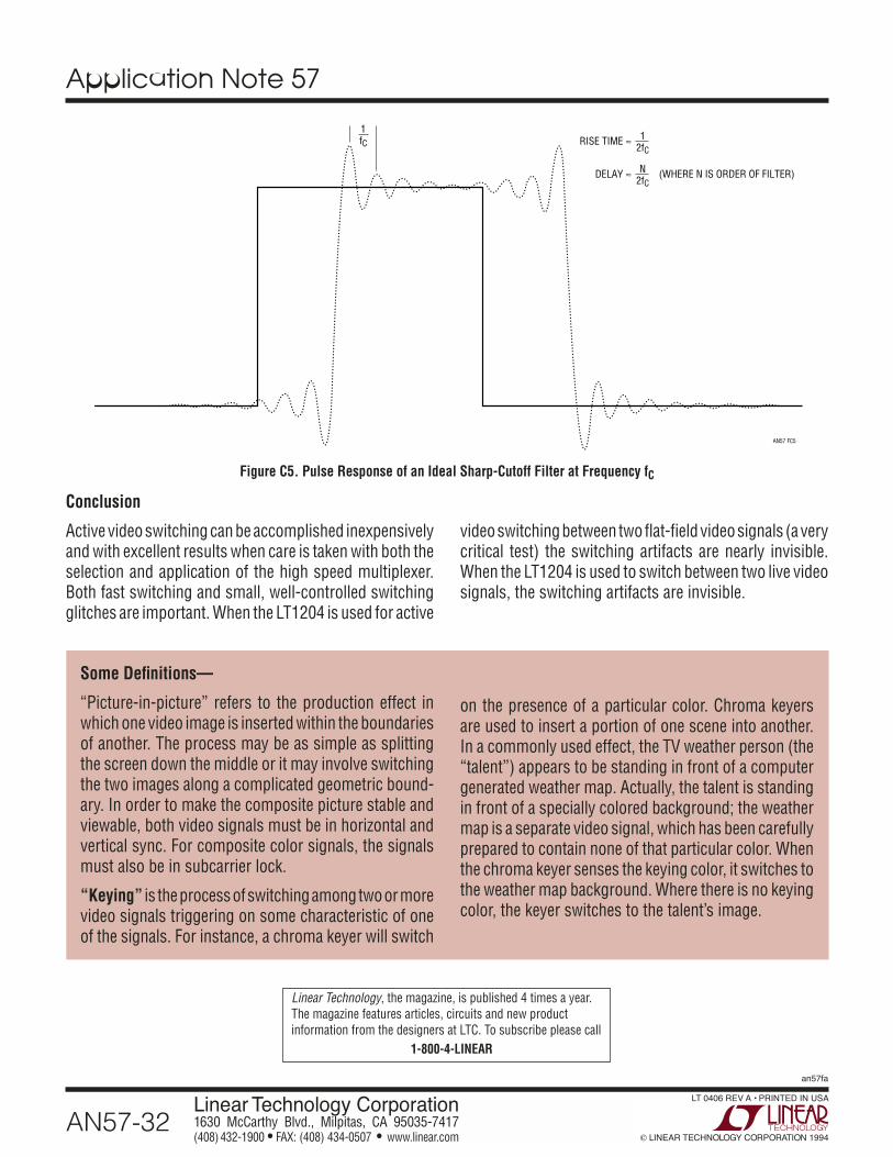
Application Note 57
AN57-32
an57fa
Linear Technology Corporation1630 McCarthy Blvd., Milpitas, CA 95035-7417 (408) 432-1900 FAX: (408) 434-0507 www.linear.com © LINEAR TECHNOLOGY CORPORATION 1994
LT 0406 REV A PRINTED IN USA
Conclusion
Active video switching can be accomplished inexpensively and with excellent results when care is taken with both the selection and application of the high speed multiplexer. Both fast switching and small, well-controlled switching glitches are important. When the LT1204 is used for active
Figure C5. Pulse Response of an Ideal Sharp-Cutoff Filter at Frequency fC
video switching between two fl at-fi eld video signals (a very critical test) the switching artifacts are nearly invisible. When the LT1204 is used to switch between two live video signals, the switching artifacts are invisible.
Some Defi nitions—
“Picture-in-picture” refers to the production effect in which one video image is inserted within the boundaries of another. The process may be as simple as splitting the screen down the middle or it may involve switching the two images along a complicated geometric bound-ary. In order to make the composite picture stable and viewable, both video signals must be in horizontal and vertical sync. For composite color signals, the signals must also be in subcarrier lock.
“Keying” is the process of switching among two or more video signals triggering on some characteristic of one of the signals. For instance, a chroma keyer will switch
on the presence of a particular color. Chroma keyers are used to insert a portion of one scene into another. In a commonly used effect, the TV weather person (the “talent”) appears to be standing in front of a computer generated weather map. Actually, the talent is standing in front of a specially colored background; the weather map is a separate video signal, which has been carefully prepared to contain none of that particular color. When the chroma keyer senses the keying color, it switches to the weather map background. Where there is no keying color, the keyer switches to the talent’s image.
Linear Technology, the magazine, is published 4 times a year. The magazine features articles, circuits and new product information from the designers at LTC. To subscribe please call
1-800-4-LINEAR
AN57 FC5
RISE TIME ≈ 12fC
DELAY ≈ N2fC
(WHERE N IS ORDER OF FILTER)
1fC