
AN4062 Application note - Home - STMicroelectronics 2013 DocID022897 Rev 3 1/17 AN4062 Application...
17
March 2013 DocID022897 Rev 3 1/17 AN4062 Application note STM32F0DISCOVERY peripheral firmware examples Introduction This application note describes the peripheral firmware examples provided for the STM32F0DISCOVERY Kit. These ready-to-run examples are provided to help the user get started quickly with STM32F0xx peripherals and STM32F0DISCOVERY board hardware. Preconfigured projects for EWARM (IAR Embedded Workbench ® for ARM ® ), MDK-ARM™, Atollic TrueSTUDIO ® and Altium TASKING ® toolchains are provided for each example. These examples are included in the firmware applications package available for download on www.st.com/stm32f0discovery. Users are advised to first read the document Getting started with software and firmware environments for the STM32F0DISCOVERY Kit (UM1523) to familiarize themselves with the STM32F0DISCOVERY Kit. Table 1 lists the microcontrollers and development tools concerned by this application note. Table 1. Applicable products and tools Type Part numbers and product categories Microcontrollers STM32F0 series Development tools STM32F0DISCOVERY Software STSW-STM32049 www.st.com
Transcript of AN4062 Application note - Home - STMicroelectronics 2013 DocID022897 Rev 3 1/17 AN4062 Application...

March 2013 DocID022897 Rev 3 1/17
AN4062Application note
STM32F0DISCOVERY peripheral firmware examples
IntroductionThis application note describes the peripheral firmware examples provided for the STM32F0DISCOVERY Kit.
These ready-to-run examples are provided to help the user get started quickly with STM32F0xx peripherals and STM32F0DISCOVERY board hardware. Preconfigured projects for EWARM (IAR Embedded Workbench® for ARM®), MDK-ARM™, Atollic TrueSTUDIO® and Altium TASKING® toolchains are provided for each example.
These examples are included in the firmware applications package available for download on www.st.com/stm32f0discovery.
Users are advised to first read the document Getting started with software and firmware environments for the STM32F0DISCOVERY Kit (UM1523) to familiarize themselves with the STM32F0DISCOVERY Kit.
Table 1 lists the microcontrollers and development tools concerned by this application note.
Table 1. Applicable products and toolsType Part numbers and product categories
Microcontrollers STM32F0 series
Development tools STM32F0DISCOVERY
Software STSW-STM32049
www.st.com

Contents AN4062
2/17 DocID022897 Rev 3
Contents
1 Peripheral firmware examples structure overview . . . . . . . . . . . . . . . . 3
2 Clock configuration . . . . . . . . . . . . . . . . . . . . . . . . . . . . . . . . . . . . . . . . . . 42.1 PLL_SOURCE_HSI . . . . . . . . . . . . . . . . . . . . . . . . . . . . . . . . . . . . . . . . . . 4
2.2 PLL_SOURCE_HSE . . . . . . . . . . . . . . . . . . . . . . . . . . . . . . . . . . . . . . . . . 4
2.3 PLL_SOURCE_HSE_BYPASS . . . . . . . . . . . . . . . . . . . . . . . . . . . . . . . . . 4
3 Peripheral firmware examples description . . . . . . . . . . . . . . . . . . . . . . . 53.1 GPIO toggle example . . . . . . . . . . . . . . . . . . . . . . . . . . . . . . . . . . . . . . . . . 5
3.2 EXTI example . . . . . . . . . . . . . . . . . . . . . . . . . . . . . . . . . . . . . . . . . . . . . . . 5
3.3 SysTick example . . . . . . . . . . . . . . . . . . . . . . . . . . . . . . . . . . . . . . . . . . . . 5
3.4 Standby mode example . . . . . . . . . . . . . . . . . . . . . . . . . . . . . . . . . . . . . . . 6
3.5 Stop mode example . . . . . . . . . . . . . . . . . . . . . . . . . . . . . . . . . . . . . . . . . . 7
3.6 Current consumption example . . . . . . . . . . . . . . . . . . . . . . . . . . . . . . . . . . 7
3.7 Flash program example . . . . . . . . . . . . . . . . . . . . . . . . . . . . . . . . . . . . . . . 8
3.8 IWDG (independent watchdog) example . . . . . . . . . . . . . . . . . . . . . . . . . . 9
3.9 ADC DMA example . . . . . . . . . . . . . . . . . . . . . . . . . . . . . . . . . . . . . . . . . . 9
3.10 ADC low power example . . . . . . . . . . . . . . . . . . . . . . . . . . . . . . . . . . . . . 10
3.11 DMA Flash RAM example . . . . . . . . . . . . . . . . . . . . . . . . . . . . . . . . . . . . 10
3.12 DMA RAM DAC example . . . . . . . . . . . . . . . . . . . . . . . . . . . . . . . . . . . . . .11
3.13 DAC signal generation example . . . . . . . . . . . . . . . . . . . . . . . . . . . . . . . . .11
3.14 TIM complementary signal example . . . . . . . . . . . . . . . . . . . . . . . . . . . . . .11
3.15 TIM time base example . . . . . . . . . . . . . . . . . . . . . . . . . . . . . . . . . . . . . . 12
3.16 TIM PWM input example . . . . . . . . . . . . . . . . . . . . . . . . . . . . . . . . . . . . . 13
3.17 TIM PWM output example . . . . . . . . . . . . . . . . . . . . . . . . . . . . . . . . . . . . 13
3.18 Timer ADC trigger example . . . . . . . . . . . . . . . . . . . . . . . . . . . . . . . . . . . 14
3.19 NVIC WFI mode example . . . . . . . . . . . . . . . . . . . . . . . . . . . . . . . . . . . . . 14
3.20 RCC (reset and clock control) example . . . . . . . . . . . . . . . . . . . . . . . . . . 15
4 Revision history . . . . . . . . . . . . . . . . . . . . . . . . . . . . . . . . . . . . . . . . . . . 16
DocID022897 Rev 3 3/17
AN4062 Peripheral firmware examples structure overview
1 Peripheral firmware examples structure overview
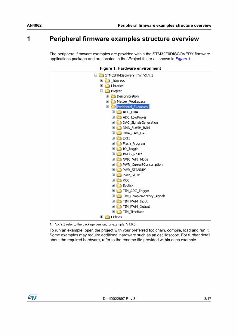
The peripheral firmware examples are provided within the STM32F0DISCOVERY firmware applications package and are located in the \Project folder as shown in Figure 1.
Figure 1. Hardware environment
1. VX.Y.Z refer to the package version, for example, V1.0.0.
To run an example, open the project with your preferred toolchain, compile, load and run it. Some examples may require additional hardware such as an oscilloscope. For further detail about the required hardware, refer to the readme file provided within each example.
Clock configuration AN4062
4/17 DocID022897 Rev 3
2 Clock configuration
The peripheral examples provided within STM32F0-Discovery Kit Firmware package are configured to run at 48 MHz, using HSI as the clock source.
However, the user can modify this configuration to use HSE (crystal or bypass mode) as the clock source, which needs some hardware modification on the discovery kit hardware.
The "system_stm32f0xx.c" file provided within each example was customized for use with the discovery kit, allowing the user to select one of the three configurations below (by un-commenting the adequate define).
2.1 PLL_SOURCE_HSI The HSI clock signal is generated from an internal 8 MHz RC Oscillator and can be used directly as a system clock, or divided by 2 to be used as a PLL input.
The HSI RC oscillator has the advantage of providing a clock source at low cost (no external components). It also has a faster startup time than the HSE crystal oscillator. However, even with a calibration, the frequency is less accurate than an external crystal oscillator or a ceramic resonator.
Note: This is the default configuration.
2.2 PLL_SOURCE_HSE The high speed external clock signal (HSE) can be generated from two possible clock sources: • HSE external crystal/ceramic resonator• HSE user external clock
The HSE crystal is not provided with the discovery kit. Some hardware modifications are necessary to connect this crystal.
For more details, refer to section “4.7 OSC clock” in “STM32F0 discovery kit User manual (UM1525)”.
2.3 PLL_SOURCE_HSE_BYPASS In this mode, the HSE is bypassed with an external clock (fixed at 8 MHz, coming from ST-Link circuit). It is used to clock the PLL, and the PLL is used as the system clock source.
Some hardware modifications are necessary to bypass the HSE with the clock coming from the ST-Link circuit.
For more details, refer to section “4.7 OSC clock” in “STM32F0 discovery kit User manual (UM1525)”.
DocID022897 Rev 3 5/17
AN4062 Peripheral firmware examples description
3 Peripheral firmware examples description
3.1 GPIO toggle examplePurpose
This example describes how to use BSRR and BRR (Port Bit Set/Reset Register High and Low) for maximum I/O toggling.
GPIO ports are connected on the AHB bus; using BSRR and BRR registers, two cycles are required to set a pin and another two cycles to reset it. So GPIO pins can toggle at AHB clock divided by 4.
Description
In this example, PC8 and PC9 (configured in push-pull output mode) toggle in a forever loop:• Set PC8 and PC9 by setting corresponding bits in BSRR register.• Reset PC8 and PC9 by setting corresponding bits in BRR register.
In this example, HCLK is configured at 48 MHz so PC8 and PC9 toggle at 12 MHz.
To achieve the maximum I/O toggling frequency, you have to configure your compiler options for high speed optimization.
3.2 EXTI examplePurpose
This example shows how to configure an external interrupt line.
Description
In this example:• PA0 pin is configured in input floating.• PA0 is configured to be used as an external interrupt source line 0 (EXTI0).• The EXTI line 0 is configured to generate an interrupt on each rising edge detected on
the PA0 pin. The interrupt is triggered every time the User push-button is pressed.• In the NVIC (nested vectored interrupt controller), the EXTI line 0 interrupt priority is
configured and the interrupt is enabled.
When the program is executed and the user pushes on the User push-button (EXTI0 interrupt routine), LED3 and LED4 connected to PC9 and PC8 are toggled.
3.3 SysTick examplePurpose
This example shows how to configure the system tick timer and use it to generate a 1 ms time base.

Peripheral firmware examples description AN4062
6/17 DocID022897 Rev 3
Description
In this example:• The system tick timer is initialized.• The system tick timer interrupt is enabled in the NVIC.• The system tick timer/counter starts in free running mode to generate periodical
interrupts.• The system tick timer interrupt is triggered every 1 ms.• A Delay function is implemented, based on the system tick timer end-of-count event.
The two LEDs, LED3 and LED4, are toggled with a timing defined by the Delay function.
3.4 Standby mode examplePurpose
This example shows how to put the system in Standby mode and wake it up from this mode using the external reset, RTC Alarm A.
Description
In this example:• The system tick timer is initialized.• The system tick timer interrupt is enabled in the NVIC.• The system tick timer/counter starts in free running mode to generate periodical
interrupts. The system tick timer interrupt is triggered every 250 ms. In the SysTick interrupt handler, LED3 is toggled; this is used to indicate whether the MCU is in STANDBY or RUN mode.
• The EXTI line 0 is configured to generate an interrupt on each rising/falling edge detected on the PA0 pin. The external interrupt is generated every time the PA0 changes levels (GND or VDD).– When a falling or rising edge is detected on the EXTI line, an interrupt is
generated. In the EXTI handler routine, the RTC is configured to generate an Alarm event in 3 seconds, after which the system enters the Standby mode and LED3 is Off.
After wake-up from Standby mode, the program execution restarts in the same way as after a reset; the RTC configuration (clock source, prescaler) is kept and LED3 is toggling again. As a result, there is no need to configure the RTC.
LED3 is used to monitor the system state as following:• LED3 toggling: system in RUN mode• LED3 off: system in STANDBY mode• LED3 toggling: system resumed from STANDBY mode
These steps are repeated in an infinite loop.
DocID022897 Rev 3 7/17
AN4062 Peripheral firmware examples description
3.5 Stop mode examplePurpose
This example shows how to enter the system to STOP mode and wake-up using EXTI Line interrupts. The EXTI Line sources are PA.0 and RTC Alarm.
Description
In this example:• The EXTI Line0 is configured to generate interrupt on falling edge.• The EXTI line17 (RTC Alarm) is configured to generate interrupt on rising edge.• The SysTick is programmed to generate an interrupt every 250 ms. In the SysTick
interrupt handler, LED3 is toggled, which indicates whether the MCU is in Stop or Run mode.
The system enters the Stop mode and waits for the RTC Alarm to be generated every 5s, or when the User push-button is pressed.
– If the RTC Alarm (EXTI_Line17) is the source of wakeup from Stop, LED3 is toggled.
– If the User push-button (EXTI_Line0) is the source of wakeup from Stop, LED4 is on and LED3 is toggled.
LEDs are used to monitor the system state:– LED3 toggling: system in Run mode; system woken up from Stop using RTC
ALARM.– LED4 on: system woken up from Stop using EXTI Line0 (User push-button).
3.6 Current consumption examplePurpose
This example shows how to configure the STM32F0xx system to measure different low power modes current consumption. The low power modes are:• Sleep mode• Stop mode with RTC• Standby mode with wake up pin (without RTC)• Standby mode with RTC
To select the low power modes to be measured, uncomment the corresponding line inside the stm32f0xx_lp_modes.h file.
Note: STM32F0xx consumption can be measured on the STM32F0DISCOVERY board by removing jumper JP2, labeled IDD, and connecting an ammeter.
Peripheral firmware examples description AN4062
8/17 DocID022897 Rev 3
Description
After reset, the program waits for the User button connected to PA.00 to be pressed to enter the selected low power mode.• When the RTC is used, the wakeup from low power mode is automatically generated
by the RTC (after 5s).• In Sleep mode and Standby mode, press again the User button to exit the low power
mode.
The different low power mode configurations are:Sleep mode– System running at PLL (48 MHz)– Flash 3 wait state– Code running from Internal Flash– All peripherals disabled– Wakeup using EXTI Line (User push-button PA.00)Stop mode– RTC clocked by LSI– Regulator in LP mode– HSI, HSE OFF and LSI if not used as RTC clock source– No IWDG– Flash in deep power down mode– Automatic Wakeup using RTC clocked by LSIStandby mode– RTC OFF– IWDG and LSI OFF– Wakeup using Wakeup Pin (PA.00) Standby mode with RTC clocked by LSI– RTC clocked by LSI– IWDG OFF and LSI OFF if not used as RTC clock source– Automatic Wakeup using RTC clocked by LSI
3.7 Flash program examplePurpose
This example describes how to program the STM32F0xx internal Flash.
Description
In this example:• After Reset, the Flash memory Program/Erase Controller is locked. The
FLASH_Unlock function is used to unlock it.• Before programming the desired addresses, an erase operation is performed using the
Flash erase sector feature. The erase procedure starts with the calculation of the

DocID022897 Rev 3 9/17
AN4062 Peripheral firmware examples description
number of sectors to be used. These sectors are erased one-by-one by calling the FLASH_EraseSector function.
• The programming operation is performed by using the FLASH_ProgramWord function. The written data is then checked and the result of the programming operation is stored in the MemoryProgramStatus variable.
3.8 IWDG (independent watchdog) examplePurpose
This example shows how to update the IWDG reload counter at regular periods, and how to simulate a software fault generating an MCU IWDG reset on expiry of a programmed time period.
Description
In this example:• The independent watchdog timeout is set to 250 ms.• The system tick is configured to generate an interrupt every 250 ms.• In the system tick interrupt service routine, the independent watchdog counter is
reloaded to prevent an independent watchdog reset, and LED4 is toggled.• The EXTI line 0 connected to PA0 pin is configured to generate an interrupt on its
falling edge.• In the NVIC, this EXTI line 0 corresponding interrupt vector is enabled with a priority
equal to 0, and the systick interrupt vector priority is set to 1 (EXTI interrupt is prior to systick interrupt).
• The EXTI line is used to simulate a firmware failure: when the EXTI line event is triggered (after pressing the User push-button on the STM32F0DISCOVERY board), the corresponding interrupt is serviced. In the ISR, LED3 turns off and the EXTI line pending bit is not cleared. The CPU executes the EXTI line ISR indefinitely and the system tick interrupt routine is never entered, so the independent watchdog counter is not reloaded. As a result, when the independent watchdog counter reaches 00, the independent watchdog generates a reset.
When the program is running and the independent watchdog reset is generated, LED4 is turned on after the system resumes operation.
3.9 ADC DMA examplePurpose
This example describes how to use ADC1 and DMA to transfer continuously converted data from ADC1 to memory.
Peripheral firmware examples description AN4062
10/17 DocID022897 Rev 3
Description
In this example: • ADC1 is configured to convert continuously the Voltage reference and the Temperature
sensor.• Each time an end of conversion occurs, the DMA transfers, in circular mode, the
converted data from ADC1 DR register to the RegularConvData_Tab[2] table.
3.10 ADC low power examplePurpose
This example provides a short description of how to use the ADC peripheral with Auto-delayed conversion mode and Auto-poweroff modes.
Description
The ADC is triggered by TIM3_TRGO which is connected to TIM3_Update Event. Each time the ADC is triggered, it converts the input voltage connected to PC.1 (which corresponds to ADC channel 11), and then the ADC enter the delay mode (no Overrun detect) until the ADC data register has been read by pressing the USER button.
Note: Connect the external signal (ranges from 0 to 3.3V) to the ADC1 pin (PC.01) to be converted.
Note: Connect an ammeter to JP2 to measure the IDD current.
3.11 DMA Flash RAM examplePurpose
This example describes how to use a DMA channel to transfer a word data buffer from a Flash memory to an embedded SRAM memory.
Description
DMA1 Channel1 is configured to transfer the contents of a 32-word data buffer, stored in the Flash memory, to the reception buffer declared in RAM.• The start of transfer is triggered by software. DMA1 Channel1 memory-to-memory
transfer is enabled. Source and destination address incrementing is also enabled. • The transfer is started by setting the Channel enable bit for DMA1 Channel1.• At the end of the transfer, a Transfer Complete interrupt is generated since it is
enabled. Once the interrupt is generated, the remaining data to be transferred is read, which must be equal to 0. The Transfer Complete Interrupt pending bit is then cleared. A comparison between the source and destination buffers is done to check that all data have been correctly transferred.

DocID022897 Rev 3 11/17
AN4062 Peripheral firmware examples description
3.12 DMA RAM DAC examplePurpose
This example provides a description of how to use a DMA channel to transfer data buffer from RAM memory to DAC.
Description
DMA1 channel3 is configured to transfer continuously, word by word, a Half-word buffer to the DAC register DAC_DHR12R. The DAC channel conversion is configured to be triggered by TIM2 TRGO triggers and without noise/triangle wave generation.12-bit right data alignment is selected since we choose to access the DAC_DHR12R register.
Note: Connect PA.04 pin to an oscilloscope.
3.13 DAC signal generation examplePurpose
This example provides a short description of how to use the DAC peripheral to generate several signals using the DMA controller.
Description
When the user presses the push-button, DMA transfers the selected waveform to DAC.• For each press on the push-button, one signal has been selected and monitored on the
DAC Channel 1• Escalator waveform (Channel 1).• Sine waveForm (Channel 1).
Note: Use the push-button connected to PA0.
Note: Connect PA4 (DAC Channel1) pin to an oscilloscope to monitor the DAC out wave.
3.14 TIM complementary signal examplePurpose
This example shows how to configure the TIM1 peripheral to generate three complementary TIM1 signals, to insert a defined dead time value, to use the break feature and to lock the desired parameters.
Description
TIM1CLK is fixed to SystemCoreClock, the TIM1 Prescaler is equal to 0 so the TIM1 counter clock used is SystemCoreClock (48 MHz).
The objective is to generate a PWM signal at 17.57 KHz:• TIM1_Period = (SystemCoreClock / 17570) - 1
Peripheral firmware examples description AN4062
12/17 DocID022897 Rev 3
The Three Duty cycles are computed as follows: – The channel 1 duty cycle is set to 50% so channel 1N is set to 50%.– The channel 2 duty cycle is set to 25% so channel 2N is set to 75%.– The channel 3 duty cycle is set to 12.5% so channel 3N is set to 87.5%.
The Timer pulse is calculated as follows:• ChannelxPulse = DutyCycle * (TIM1_Period - 1) / 100
A dead time equal to 11/SystemCoreClock is inserted between the different complementary signals, and the Lock level 1 is selected.The break Polarity is used at High level.
The TIM1 waveform can be displayed using an oscilloscope.• Connect the TIM1 pins to an oscilloscope to monitor the different waveforms:
– TIM1_CH1 pin (PA.08) – TIM1_CH1N pin (PB.13) – TIM1_CH2 pin (PA.9) – TIM1_CH2N pin (PB.14) – TIM1_CH3 pin (PA.10) – TIM1_CH3N pin (PB.15)
• Connect the TIM1 break pin TIM1_BKIN pin (PB.12) to the GND. To generate a break event, switch this pin level from 0V to 3.3V.
3.15 TIM time base examplePurpose
This example shows how to configure the TIM peripheral in Output Compare Timing mode with the corresponding Interrupt requests for each channel, in order to generate 2 different time bases.
Description
The TIM3CLK frequency is set to SystemCoreClock (Hz), to get TIM3 counter clock at 6 MHz so the Prescaler is computed as follows:• Prescaler = (TIM3CLK / TIM3 counter clock) - 1.• SystemCoreClock is set to 48 MHz.• The TIM3 CC3 register is equal to 13654, CC3 update rate = TIM3 counter clock /
CCR3_Val = 439.4 Hz.Thus, the TIM3 Channel 3 generates an interrupt every 2.27 ms.
• The TIM3 CC4 register is equal to 6826, CC4 update rate = TIM3 counter clock / CCR4_Val = 878.9 Hz.Thus, the TIM3 Channel 4 generates an interrupt every 1.13 ms.
When the counter value reaches the Output compare registers values, the Output Compare interrupts are generated and, in the handler routine, 2 LEDs (LED3 and LED4) connected to PC08 and PC09 are toggled with the following frequencies:
– LED3(PC09): 219.7 Hz (CC3) – LED4(PC08): 439.4 Hz (CC4)

DocID022897 Rev 3 13/17
AN4062 Peripheral firmware examples description
3.16 TIM PWM input examplePurpose
This example shows how to use the TIM peripheral to measure the frequency and duty cycle of an external signal.
Description
The TIMxCLK frequency is set to SystemCoreClock, the Prescaler is 0 so the counter clock is SystemCoreClock. SystemCoreClock is set to 48 MHz for STM32F0xx Devices.
TIM2 is configured in PWM Input Mode: the external signal is connected to TIM2 Channel2 used as an input pin.
To measure the frequency and the duty cycle, we use the TIM2 CC2 interrupt request, so that the frequency and the duty cycle of the external signal are computed In the TIM2_IRQHandler routine.
The “Frequency” variable contains the external signal frequency:• TIM2 counter clock = SystemCoreClock,• Frequency = TIM2 counter clock / TIM2_CCR2 in Hz,
The “DutyCycle” variable contains the external signal duty cycle: – DutyCycle = (TIM2_CCR1*100)/(TIM2_CCR2) in %.
The minimum frequency value to measure is 732 Hz (TIM2 counter clock / CCR MAX).
Note: Connect the external signal to measure the TIM2 CH2 pin (PA.01).
3.17 TIM PWM output examplePurpose
This example shows how to configure the TIM1 peripheral to generate PWM signals with 4 different duty cycles (50%, 37.5%, 25% and 12.5%).
Description
The TIMxCLK frequency is set to SystemCoreClock, the Prescaler is 0 so the counter clock is SystemCoreClock. SystemCoreClock is set to 48 MHz for STM32F0xx Devices.
Peripheral firmware examples description AN4062
14/17 DocID022897 Rev 3
The objective is to generate a PWM signal at 17.57 KHz:– TIM1_Period = (SystemCoreClock / 17570) - 1– TIM1 Frequency = TIM1 counter clock/(ARR + 1) = 48 MHz / 2730 = 17.57 kHz
• The TIM1 CCR1 register value is equal to 1364, so the TIM1 Channel 1 generates a PWM signal with a frequency equal to 17.57 kHz and a duty cycle equal to 50%:
TIM1 Channel1 duty cycle = (TIM1_CCR1/ TIM1_ARR + 1)* 100 = 50%• The TIM1 CCR2 register value is equal to 1023, so the TIM1 Channel 2 generates a
PWM signal with a frequency equal to 17.57 kHz and a duty cycle equal to 37.5%:TIM1 Channel2 duty cycle = (TIM1_CCR2/ TIM1_ARR + 1)* 100 = 37.5%
• The TIM1 CCR3 register value is equal to 682, so the TIM1 Channel 3 generates a PWM signal with a frequency equal to 17.57 kHz and a duty cycle equal to 25%:
TIM1 Channel3 duty cycle = (TIM1_CCR3/ TIM1_ARR + 1)* 100 = 25%• The TIM1 CCR4 register value is equal to 431, so the TIM1 Channel 4 generates a
PWM signal with a frequency equal to 17.57 kHz and a duty cycle equal to 12.5%:TIM1 Channel4 duty cycle = (TIM1_CCR4/ TIM1_ARR + 1)* 100 = 12.5%
Note: The PWM waveform can be displayed using an oscilloscope. Connect the TIM1 pins to an oscilloscope to monitor the different waveforms:• TIM1_CH1 pin (PA.08)• TIM1_CH2 pin (PA.09)• TIM1_CH3 pin (PA.10)• TIM1_CH4 pin (PA.11)
3.18 Timer ADC trigger examplePurpose
This example describes how to configure the TIM to trigger the ADC conversion.
Description
In this example, the TIM1 is configured in PWM mode, the TIM1 CC4 event is used to trigger the ADC.
The ADC is configured to convert continuously the ADC_Channel_11 (connected to an external voltage).
Each time the TIM1 CC4 event occurs, the ADC converts the variable voltage.
Note: Connect the external signal ranges between 0 and 3.3V to ADC pin (PC.01).
3.19 NVIC WFI mode examplePurpose
This example shows how to enter the WFI mode and wake up from this mode by the User key interrupt.
DocID022897 Rev 3 15/17
AN4062 Peripheral firmware examples description
Description
In the associated software, the system clock is set to 48 MHz. When the user presses the User Key Button, the MCU enters the WFI mode. If the user presses again the User Key Button, LED3 is toggled with a frequency depending on the system clock. This is used to indicate whether the MCU is in WFI or RUN mode. • Pressing the key push-button (generates a rising edge on EXTI Line0) will put the core
in the WFI mode, causing the LED3 to stop toggling.• To wake up from the WFI mode, you have to press again the button; it generates an
interrupt, which exits the system from the WFI mode. LED3 restarts toggling.
Note: Press the User button to enter and exit the WFI mode.
3.20 RCC (reset and clock control) examplePurpose
This example shows how to:• Configure the HSE (High Speed Clock) as an RCC clock• Use the Clock Security System (CSS) feature to generate an NMI interrupt• Output the system clock on MCO
Description
For debug purposes, the RCC_GetClocksFreq() function is used to retrieve the current status and frequencies of different on-chip clocks.
You can see the RCC_ClockFreq structure content, which holds the frequencies of different on-chip clocks, using your toolchain debugger.
This example also handles the High Speed External clock (HSE) failure detection: when the HSE clock disappears (broken or disconnected external Quartz), HSE and PLL are disabled (but no change to PLL configuration), HSI is selected as a system clock source and an interrupt (NMI) is generated. In the NMI ISR, the HSE and HSE ready interrupt are enabled. Once the HSE clock recovers, the HSERDY interrupt is generated and, in the RCC ISR routine, the system clock is reconfigured to its previous state (before HSE clock failure). You can monitor the system clock on MCO pin (PA.8).
Two LEDs are toggled with a timing defined by the Delay function.

Revision history AN4062
16/17 DocID022897 Rev 3
4 Revision history
Table 2. Document revision historyDate Revision Changes
23-Mar-2012 1 Initial release.
14-May-2012 2 Section 2: Clock configuration added.
28-Mar-2013 3 Updated Table 1: Applicable products and tools and Section 3.1: GPIO toggle example.

DocID022897 Rev 3 17/17
AN4062
Please Read Carefully:
Information in this document is provided solely in connection with ST products. STMicroelectronics NV and its subsidiaries (“ST”) reserve theright to make changes, corrections, modifications or improvements, to this document, and the products and services described herein at anytime, without notice.
All ST products are sold pursuant to ST’s terms and conditions of sale.
Purchasers are solely responsible for the choice, selection and use of the ST products and services described herein, and ST assumes noliability whatsoever relating to the choice, selection or use of the ST products and services described herein.
No license, express or implied, by estoppel or otherwise, to any intellectual property rights is granted under this document. If any part of thisdocument refers to any third party products or services it shall not be deemed a license grant by ST for the use of such third party productsor services, or any intellectual property contained therein or considered as a warranty covering the use in any manner whatsoever of suchthird party products or services or any intellectual property contained therein.
UNLESS OTHERWISE SET FORTH IN ST’S TERMS AND CONDITIONS OF SALE ST DISCLAIMS ANY EXPRESS OR IMPLIEDWARRANTY WITH RESPECT TO THE USE AND/OR SALE OF ST PRODUCTS INCLUDING WITHOUT LIMITATION IMPLIEDWARRANTIES OF MERCHANTABILITY, FITNESS FOR A PARTICULAR PURPOSE (AND THEIR EQUIVALENTS UNDER THE LAWSOF ANY JURISDICTION), OR INFRINGEMENT OF ANY PATENT, COPYRIGHT OR OTHER INTELLECTUAL PROPERTY RIGHT.
ST PRODUCTS ARE NOT AUTHORIZED FOR USE IN WEAPONS. NOR ARE ST PRODUCTS DESIGNED OR AUTHORIZED FOR USEIN: (A) SAFETY CRITICAL APPLICATIONS SUCH AS LIFE SUPPORTING, ACTIVE IMPLANTED DEVICES OR SYSTEMS WITHPRODUCT FUNCTIONAL SAFETY REQUIREMENTS; (B) AERONAUTIC APPLICATIONS; (C) AUTOMOTIVE APPLICATIONS ORENVIRONMENTS, AND/OR (D) AEROSPACE APPLICATIONS OR ENVIRONMENTS. WHERE ST PRODUCTS ARE NOT DESIGNEDFOR SUCH USE, THE PURCHASER SHALL USE PRODUCTS AT PURCHASER’S SOLE RISK, EVEN IF ST HAS BEEN INFORMED INWRITING OF SUCH USAGE, UNLESS A PRODUCT IS EXPRESSLY DESIGNATED BY ST AS BEING INTENDED FOR “AUTOMOTIVE,AUTOMOTIVE SAFETY OR MEDICAL” INDUSTRY DOMAINS ACCORDING TO ST PRODUCT DESIGN SPECIFICATIONS.PRODUCTS FORMALLY ESCC, QML OR JAN QUALIFIED ARE DEEMED SUITABLE FOR USE IN AEROSPACE BY THECORRESPONDING GOVERNMENTAL AGENCY.
Resale of ST products with provisions different from the statements and/or technical features set forth in this document shall immediately voidany warranty granted by ST for the ST product or service described herein and shall not create or extend in any manner whatsoever, anyliability of ST.
ST and the ST logo are trademarks or registered trademarks of ST in various countries.Information in this document supersedes and replaces all information previously supplied.
The ST logo is a registered trademark of STMicroelectronics. All other names are the property of their respective owners.
© 2013 STMicroelectronics - All rights reserved
STMicroelectronics group of companies
Australia - Belgium - Brazil - Canada - China - Czech Republic - Finland - France - Germany - Hong Kong - India - Israel - Italy - Japan - Malaysia - Malta - Morocco - Philippines - Singapore - Spain - Sweden - Switzerland - United Kingdom - United States of America
www.st.com


