AN292 Wideband / Dual Band WLAN LNA using …„¢, primarion™, primepack™, primestack™,...
30
RF and Protection Devices BFR840L3RHESD Application Note AN292 Revision: Rev. 1.0 2012-08-14 BFR840L3RHESD SiGe:C Ultra Low Noise RF Transistor in Low Parts Count Wideband / Dual Band 2.4 – 5.8 GHz WLAN LNA Application „0201‟ case size passives < 1 microsecond Turn-On / Turn-Off Time 18.5 dB Gain, 1.1 dB Noise Figure at 2.4 GHz; 14.1 dB Gain, 1.4 dB Noise Figure at 5.8 GHz (For 802.11a / ac / b / g / n Wireless LAN Applications)
Transcript of AN292 Wideband / Dual Band WLAN LNA using …„¢, primarion™, primepack™, primestack™,...

RF and Protect ion Devices
BFR840L3RHESD
Appl icat ion Note AN292 Revision: Rev. 1.0
2012-08-14
BFR840L3RHESD SiGe:C Ultra Low Noise RF Transistor in Low Parts Count Wideband / Dual Band 2.4 – 5.8 GHz WLAN LNA Application „0201‟ case size passives < 1 microsecond Turn-On / Turn-Off Time 18.5 dB Gain, 1.1 dB Noise Figure at 2.4 GHz; 14.1 dB Gain, 1.4 dB Noise Figure at 5.8 GHz
(For 802.11a / ac / b / g / n Wireless LAN Applications)
Edition 2012-08-14
Published by Infineon Technologies AG 81726 Munich, Germany
© 2012 Infineon Technologies AG All Rights Reserved.
Legal Disclaimer
The information given in this document shall in no event be regarded as a guarantee of conditions or characteristics. With respect to any examples or hints given herein, any typical values stated herein and/or any information regarding the application of the device, Infineon Technologies hereby disclaims any and all warranties and liabilities of any kind, including without limitation, warranties of non-infringement of intellectual property rights of any third party.
Information
For further information on technology, delivery terms and conditions and prices, please contact the nearest Infineon Technologies Office (www.infineon.com).
Warnings
Due to technical requirements, components may contain dangerous substances. For information on the types in question, please contact the nearest Infineon Technologies Office.
Infineon Technologies components may be used in life-support devices or systems only with the express written approval of Infineon Technologies, if a failure of such components can reasonably be expected to cause the failure of that life-support device or system or to affect the safety or effectiveness of that device or system. Life support devices or systems are intended to be implanted in the human body or to support and/or maintain and sustain and/or protect human life. If they fail, it is reasonable to assume that the health of the user or other persons may be endangered.

BFR840L3RHESD BFR840L3RHESD 2.4 - 5.8 GHz Dualband WLAN LNA
Application Note AN292, Rev. 1.0 2012-08-14 3 / 30
Application Note AN292
Revision History: 2012-08-14
Previous Revision: No previous revision
Page Subjects (major changes since last revision)
Trademarks of Infineon Technologies AG
AURIX™, C166™, CanPAK™, CIPOS™, CIPURSE™, EconoPACK™, CoolMOS™, CoolSET™, CORECONTROL™, CROSSAVE™, DAVE™, DI-POL™, EasyPIM™, EconoBRIDGE™, EconoDUAL™, EconoPIM™, EconoPACK™, EiceDRIVER™, eupec™, FCOS™, HITFET™, HybridPACK™, I²RF™, ISOFACE™, IsoPACK™, MIPAQ™, ModSTACK™, my-d™, NovalithIC™, OptiMOS™, ORIGA™, POWERCODE™, PRIMARION™, PrimePACK™, PrimeSTACK™, PRO-SIL™, PROFET™, RASIC™, ReverSave™, SatRIC™, SIEGET™, SINDRION™, SIPMOS™, SmartLEWIS™, SOLID FLASH™, TEMPFET™, thinQ!™, TRENCHSTOP™, TriCore™.
Other Trademarks
Advance Design System™ (ADS) of Agilent Technologies, AMBA™, ARM™, MULTI-ICE™, KEIL™, PRIMECELL™, REALVIEW™, THUMB™, µVision™ of ARM Limited, UK. AUTOSAR™ is licensed by AUTOSAR development partnership. Bluetooth™ of Bluetooth SIG Inc. CAT-iq™ of DECT Forum. COLOSSUS™, FirstGPS™ of Trimble Navigation Ltd. EMV™ of EMVCo, LLC (Visa Holdings Inc.). EPCOS™ of Epcos AG. FLEXGO™ of Microsoft Corporation. FlexRay™ is licensed by FlexRay Consortium. HYPERTERMINAL™ of Hilgraeve Incorporated. IEC™ of Commission Electrotechnique Internationale. IrDA™ of Infrared Data Association Corporation. ISO™ of INTERNATIONAL ORGANIZATION FOR STANDARDIZATION. MATLAB™ of MathWorks, Inc. MAXIM™ of Maxim Integrated Products, Inc. MICROTEC™, NUCLEUS™ of Mentor Graphics Corporation. MIPI™ of MIPI Alliance, Inc. MIPS™ of MIPS Technologies, Inc., USA. muRata™ of MURATA MANUFACTURING CO., MICROWAVE OFFICE™ (MWO) of Applied Wave Research Inc., OmniVision™ of OmniVision Technologies, Inc. Openwave™ Openwave Systems Inc. RED HAT™ Red Hat, Inc. RFMD™ RF Micro Devices, Inc. SIRIUS™ of Sirius Satellite Radio Inc. SOLARIS™ of Sun Microsystems, Inc. SPANSION™ of Spansion LLC Ltd. Symbian™ of Symbian Software Limited. TAIYO YUDEN™ of Taiyo Yuden Co. TEAKLITE™ of CEVA, Inc. TEKTRONIX™ of Tektronix Inc. TOKO™ of TOKO KABUSHIKI KAISHA TA. UNIX™ of X/Open Company Limited. VERILOG™, PALLADIUM™ of Cadence Design Systems, Inc. VLYNQ™ of Texas Instruments Incorporated. VXWORKS™, WIND RIVER™ of WIND RIVER SYSTEMS, INC. ZETEX™ of Diodes Zetex Limited.
Last Trademarks Update 2011-11-11

BFR840L3RHESD BFR840L3RHESD 2.4 - 5.8 GHz Dualband WLAN LNA
List of Content, Figures and Tables
Application Note AN292, Rev. 1.0 2012-08-14 4 / 30
Table of Contents
1 Introduction ........................................................................................................................................ 5
3 Schematic ........................................................................................................................................... 7
2 Measured Graphs ............................................................................................................................... 9
3 Evaluation Board and Layout Information .................................................................................... 27
4 Author ................................................................................................................................................ 29
5 Remark .............................................................................................................................................. 29
List of Figures
Figure 1 Block Diagram of low-cost WLAN application with Dual Band LNA .................................................... 6 Figure 2 Schematic Diagram .............................................................................................................................. 7 Figure 3 Noise Figure, 2.4 – 6 GHz Wideband / Dual Band LNA ..................................................................... 9 Figure 4 Noise Figure, Tabular Data ................................................................................................................ 10 Figure 5 Amplifier Gain compression at 2400 MHz .......................................................................................... 11 Figure 6 Amplifier Gain Compression at 5825 MHz ........................................................................................ 12 Figure 7 Amplifier stability factor “µ1” ............................................................................................................... 13 Figure 8 Input Match of Broadband / Dual Band LNA ..................................................................................... 14 Figure 9 Input Matching of the Broadband / Dual Band LNA, Smith Chart ...................................................... 15 Figure 10 Wideband Gain of Amplifier, DC Power ON ...................................................................................... 16 Figure 11 Wideband Gain of Amplifier, DC POWER OFF ................................................................................. 17 Figure 12 Reverse Isolation, DC power ON ....................................................................................................... 18 Figure 13 Reverse Isolation, DC Power OFF ..................................................................................................... 19 Figure 14 Amplifier Wideband Output Return Loss ............................................................................................ 20 Figure 15 Amplifier Output Return Loss, Smith Chart ........................................................................................ 21 Figure 16 Amplifier Input 3
rd Order Intercept Point Measurement, 2400 MHz ................................................... 22
Figure 17 Amplifier Input 3rd
Order Intercept Point Measurement, 5825 MHz ................................................... 23 Figure 18 Diagram of setup for making amplifier turn-on and turn-off times. ..................................................... 24 Figure 19 Oscilloscope screen shot, amplifier turn-on time ............................................................................... 25 Figure 20 Oscilloscope screen-shot, amplifier turn-off time ............................................................................... 26 Figure 21 View of Entire PC Board .................................................................................................................... 27 Figure 22 Close-In View of LNA Section. ......................................................................................................... 28 Figure 23 PC Board Cross-Section Information. ................................................................................................ 29
List of Tables
Table 1 Summary of Measurement Results ...................................................................................................... 6 Table 2 Bill-of-Materials ..................................................................................................................................... 7

BFR840L3RHESD BFR840L3RHESD 2.4 - 5.8 GHz Dualband WLAN LNA
Application Note AN292, Rev. 1.0 2012-08-14 5 / 30
1 Introduction
1.1 Device Overview: BFR840L3RHESD
Infineon Technologies‟ BFR840L3RHESD is a high gain, ultra low noise Silicon-Germanium-
Carbon (SiGe:C) HBT device suitable for a wide range of Low Noise Amplifier (LNA)
applications. This RF Transistor has integrated protection structures to guard against Electro
Static Discharge (ESD) events up to 1.5kV per the Human Body Model (HBM), and these
same structures also protect the transistor against damage caused by excessive RF input
power levels up to +20 dBm. The device is housed in the RoHS-compliant, Halogen-free
TSLP-3-9 leadless package, which is only 1.0 x 0.6 x 0.31mm. The 0.31mm package height
makes this transistor a good choice for RF Module applications.
1.2 Circuitry
The circuit shown is targeted for Wireless LAN (WLAN) 802.11a / ac / b / g / n applications
where lowest possible cost, low external parts count, and high receiver sensitivity / long
range are primary goals. “0201” case size passives are used througout. Resistive
Feedback is used to achieve unconditional stability and a good broadband 50 ohm match at
both input and output. Feedback also makes the amplifier more tolerant of component &
device variation, as well as making the design more forgiving of variations in PC board
layout. The price paid for using feedback is a slight increase in amplifier noise figure, as well
as some decrease in gain. (The penalty paid in Noise Figure from the feedback is
approximately 0.4 dB at 2.4 GHz, and ~0.3 dB at 5 – 6 GHz). The LNA may be used as either
a single-band amplifier at 2.4 or at 5 – 6 GHz with no changes made to the element values,
or the LNA may be used in a dualband configuration where both WLAN bands are amplified
together in a single device, i.e. for legacy systems where Dual Band Dual Concurrent
operation is not required (refer to Figure 1). This simplification and commonality allows the
end user to use one LNA design across his or her different systems, at either WLAN
frequency band, simplifying logistics and reducing design effort. Potential applications may
include WLAN transceivers used in Access Points, laptop PCs, Tablets, Gaming Consoles,
USB dongles, etc. Generally, LNA‟s for these applications must be able to switch on & off
within about 1 microsecond or less. The charge storage (capacitance) used in this circuit is

BFR840L3RHESD BFR840L3RHESD 2.4 - 5.8 GHz Dualband WLAN LNA
Application Note AN292, Rev. 1.0 2012-08-14 6 / 30
minimized to reduce on / off times, and this LNA achieves a switching time of ~ 15
nanoseconds. One potential trade-off for reduced capacitance values is a reduction in Third
Order Intercept (IP3) performance. The good wideband match of the LNA – with an input
and output return loss of -10 dB or better across the entire 2.4 – 6 GHz frequency range -
makes integrating the amplifier with other system blocks (filters, switches, diplexers, etc.)
faster, easier and more predictable, reducing risk and time-to-market. No external emitter
degeneration is required. The LNA is unconditionally stable over the 50 MHz – 12 GHz
frequency range. External parts count (not including BFR840L3RHESD transistor) is 8; 4
capacitors, 3 resistors, and 1 chip inductors. All passives are „0201‟ case size. At 2.4 GHz,
the amplifier achieves ~ 18 dB gain with a Noise Figure of 1.1 dB, while at 5.8 GHz, the gain
is ~ 14 dB with a Noise Figure of 1.4 dB.
Low-Cost
LC Diplexer
WLAN
RF ASIC
5 – 6 GHz Rx
2.4 GHz Rx
HPF
LPF
Tx / Rx
Switch
Dual Band
WLAN LNA
2.4 – 5.8 GHz
Broadband
Antenna
Rx
Tx
Tx Path
Figure 1 Block Diagram of low-cost WLAN application with Dual Band LNA
Table 1 Summary of Measurement Results

BFR840L3RHESD BFR840L3RHESD 2.4 - 5.8 GHz Dualband WLAN LNA
Application Note AN292, Rev. 1.0 2012-08-14 7 / 30
3 Schematic Diagram
Figure 2 Schematic Diagram
Table 2 Bill-of-Materials
Symbol Value Unit Size Manufacturer Comment
C1
10
pF
0201
Various
Input DC block
C2
10
pF
0201
Various
DC block for RF Feedback path
C3
1.8
pF
0201
Various
Output DC block; also influences input and output matching
PCB = 840L3RHESD-120507 Rev A
PC Board Material = Standard FR4
Layer spacing (top RF to internal ground plane): 0.010 inch / 0.25 mm
Q1
BFR840L3RHESD
RF Transistor
TSLP-3-9 Package
J1
RF INPUT
C110 pF
(0201)
I = 9.4 mA (nominal)
R133K
(0201)
C433 pF(0201)
R3
120 ohms(0201)
Vcc
= 3.0V
J3DC Connector
C3
1.8 pF
(0201)
R2
1K
(0201)
C2
10 pF
(0201)
All passives are "0201" case size
Inductor L1 is MuRata LQP03T_02 Series
Total of 8 external elements:4 x "C"
3 x "R"
1 x "L"
BFR840L3RHESD Wideband / Dual Band WLAN Feedback LNA
50 ohm trace
50 ohm trace
J2L1
6.2 nH
(0201)
DC Operating Point @ T=25 C:
VCC
= 3.0 V
I = 9.4 mA
VCE(Q1)
= 1.87 V

BFR840L3RHESD BFR840L3RHESD 2.4 - 5.8 GHz Dualband WLAN LNA
Application Note AN292, Rev. 1.0 2012-08-14 8 / 30
Table 2 Bill-of-Materials
Symbol Value Unit Size Manufacturer Comment
C4 33 pF 0201 Various RF decoupling / lower frequency decoupling / blocking cap. Strongest influence on Turn-On / Turn-Off time. Value was minimized to speed up ON-OFF and OFF-ON time
L1 6.2 nH 0201 Murata LQP03T series. RF choke at LNA output. Influences output match
R1 33K Ohm 0201 Various DC biasing
R2 1K Ohm 0201 Various RF feedback resistor, output (collector) to input (base). Provides wideband matching, improves stability margin at price of reduced gain and slightly degraded noise figure (~ 0.1 dB).
R3 120 Ohm 0201 Various DC biasing. Drolps supply voltage below transistor‟s safe limit (VCE); also provides some DC negative feedback to stabilize DC operating point of transistor over temperature, hFE variation of transistor, etc.
Q1 --- --- TSLP-3-9
1.0 x 0.6 x 0.31mm
Infineon Technologies
BFR840L3RHESD SiGe:C RF Transistor
J1, J2 --- --- --- Emerson – Johnson
RF edge Mount SMA Female Connector, 142-0701-841 (Input, Output RF Connectors)
J3 --- --- --- Tyco (AMP) 5 Pin DC connector header, MTA-100 Series, 640456-5

BFR840L3RHESD BFR840L3RHESD 2.4 - 5.8 GHz Dualband WLAN LNA
Application Note AN292, Rev. 1.0 2012-08-14 9 / 30
2 Measured Graphs
Noise Figure Plot. From Rohde & Schwarz FS-K3 + FSEM30.
System preamplifier = MITEQ AFS3-00101200-22-10P-4-HS.
Noise Source = Agilent 346A
Figure 3 Noise Figure, 2.4 – 6 GHz Wideband / Dual Band LNA

BFR840L3RHESD BFR840L3RHESD 2.4 - 5.8 GHz Dualband WLAN LNA
Application Note AN292, Rev. 1.0 2012-08-14 10 / 30
Figure 4 Noise Figure, Tabular Data
BFR840L3RHESD BFR840L3RHESD 2.4 - 5.8 GHz Dualband WLAN LNA
Application Note AN292, Rev. 1.0 2012-08-14 11 / 30
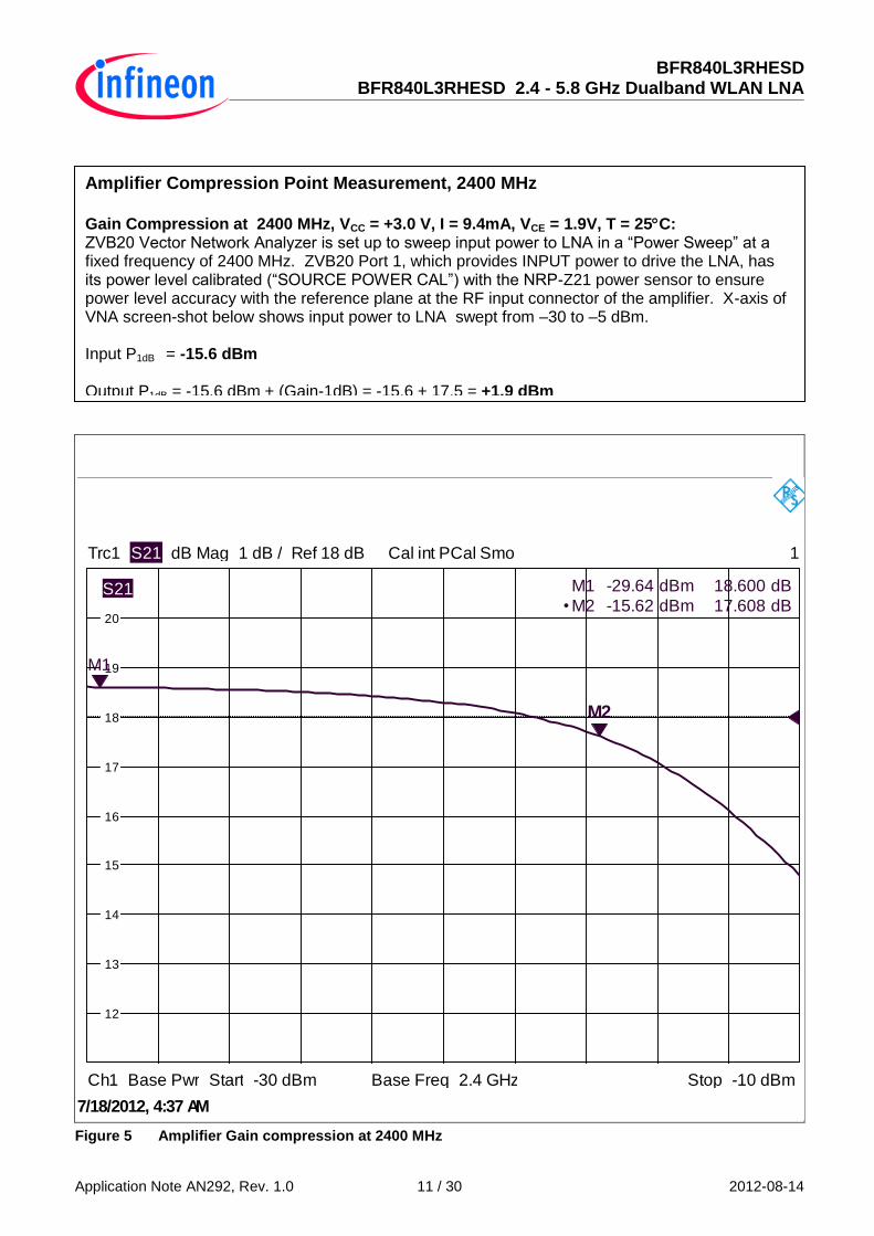
Figure 5 Amplifier Gain compression at 2400 MHz
12
13
14
15
16
17
18
19
20
18
1
Base Freq 2.4 GHzCh1 Base Pwr Start -30 dBm Stop -10 dBm
Trc1 S21 dB Mag 1 dB / Ref 18 dB Cal int PCal Smo
•
M1
M2
-29.64
-15.62
dBm
dBm
18.600
17.608
dB
dB S21
M1
M2
7/18/2012, 4:37 AM
Amplifier Compression Point Measurement, 2400 MHz Gain Compression at 2400 MHz, VCC = +3.0 V, I = 9.4mA, VCE = 1.9V, T = 25C: ZVB20 Vector Network Analyzer is set up to sweep input power to LNA in a “Power Sweep” at a fixed frequency of 2400 MHz. ZVB20 Port 1, which provides INPUT power to drive the LNA, has its power level calibrated (“SOURCE POWER CAL”) with the NRP-Z21 power sensor to ensure power level accuracy with the reference plane at the RF input connector of the amplifier. X-axis of VNA screen-shot below shows input power to LNA swept from –30 to –5 dBm. Input P1dB = -15.6 dBm Output P1dB = -15.6 dBm + (Gain-1dB) = -15.6 + 17.5 = +1.9 dBm
BFR840L3RHESD BFR840L3RHESD 2.4 - 5.8 GHz Dualband WLAN LNA
Application Note AN292, Rev. 1.0 2012-08-14 12 / 30
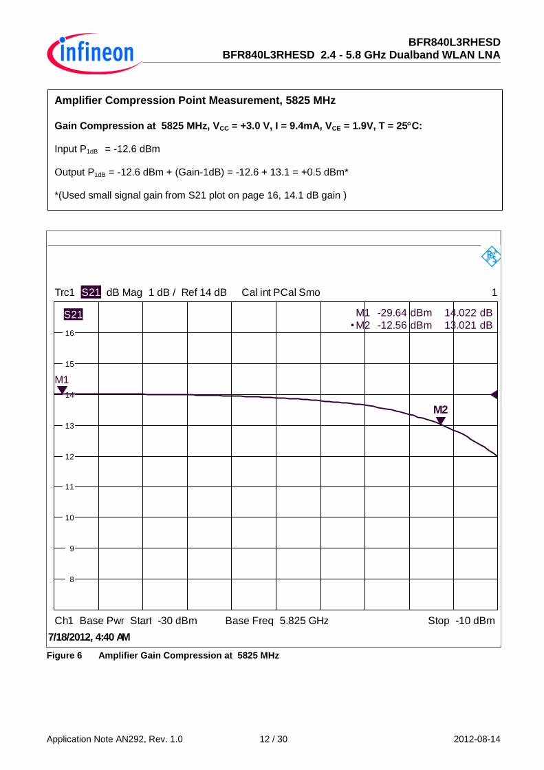
Figure 6 Amplifier Gain Compression at 5825 MHz
8
9
10
11
12
13
14
15
16
14
1
Base Freq 5.825 GHzCh1 Base Pwr Start -30 dBm Stop -10 dBm
Trc1 S21 dB Mag 1 dB / Ref 14 dB Cal int PCal Smo
•
M1
M2
-29.64
-12.56
dBm
dBm
14.022
13.021
dB
dB S21
M1
M2
7/18/2012, 4:40 AM
Amplifier Compression Point Measurement, 5825 MHz Gain Compression at 5825 MHz, VCC = +3.0 V, I = 9.4mA, VCE = 1.9V, T = 25C: Input P1dB = -12.6 dBm Output P1dB = -12.6 dBm + (Gain-1dB) = -12.6 + 13.1 = +0.5 dBm* *(Used small signal gain from S21 plot on page 16, 14.1 dB gain )

BFR840L3RHESD BFR840L3RHESD 2.4 - 5.8 GHz Dualband WLAN LNA
Application Note AN292, Rev. 1.0 2012-08-14 13 / 30
Rohde and Schwarz ZVB Network Analyzer Calculates and plots stability factor “1” of the
BFR840L3RHESD Wideband LNA in real time. Stability Factor 1 is defined as follows [1]:
1 - |S11|2
1 =
| S22 – S11* det(S) | + |S21S12|
The necessary & sufficient condition for Unconditional Stability is 1 > 1.0. In the plot, 1 >
1.0 over 10 MHz – 12 GHz; amplifier is Unconditionally Stable over 50 MHz – 12 GHz frequency range.
Figure 7 Amplifier stability factor “µ1”
800
900
1000
1100
1200
1300
1400
1500
1600
1000
1
Base Pwr -25 dBm Ch1 Base Freq Start 50 MHz Stop 12 GHz
Trc1 µ1 Lin Mag 100 mU/ Ref 1 U Cal Smo
•
M1
M2
M3
M4
M5
2.400000
2.483500
4.900000
5.825000
1.405000
GHz
GHz
GHz
GHz
GHz
1.0437
1.0504
1.2391
1.2834
1.0107
U
U
U
U
U
µ1
M1M2
M3
M4
M5
7/18/2012, 1:28 AM
BFR840L3RHESD BFR840L3RHESD 2.4 - 5.8 GHz Dualband WLAN LNA
Application Note AN292, Rev. 1.0 2012-08-14 14 / 30
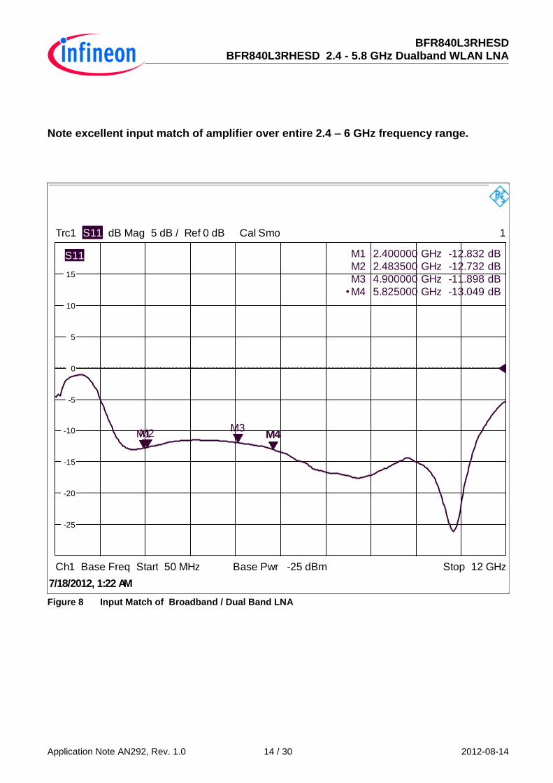
Note excellent input match of amplifier over entire 2.4 – 6 GHz frequency range.
Figure 8 Input Match of Broadband / Dual Band LNA
-25
-20
-15
-10
-5
0
5
10
15
0
1
Base Pwr -25 dBm Ch1 Base Freq Start 50 MHz Stop 12 GHz
Trc1 S11 dB Mag 5 dB / Ref 0 dB Cal Smo
•
M1
M2
M3
M4
2.400000
2.483500
4.900000
5.825000
GHz
GHz
GHz
GHz
-12.832
-12.732
-11.898
-13.049
dB
dB
dB
dB
S11
M1M2M3
M4
7/18/2012, 1:22 AM
BFR840L3RHESD BFR840L3RHESD 2.4 - 5.8 GHz Dualband WLAN LNA
Application Note AN292, Rev. 1.0 2012-08-14 15 / 30
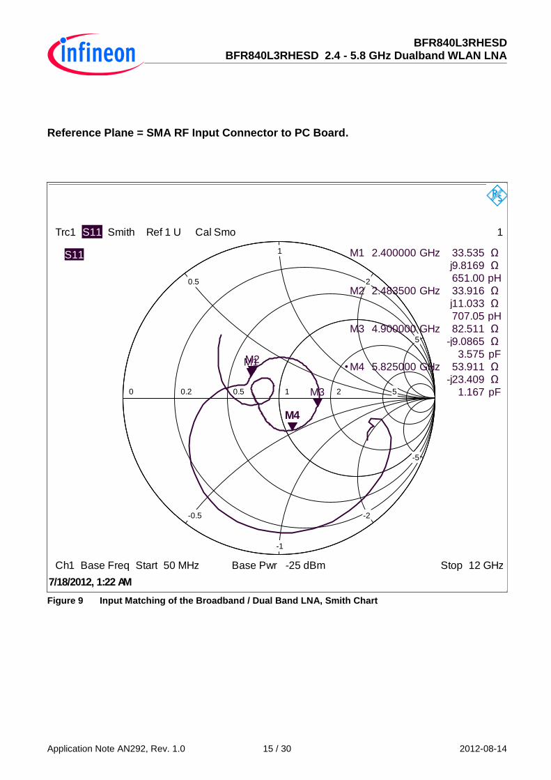
Reference Plane = SMA RF Input Connector to PC Board.
Figure 9 Input Matching of the Broadband / Dual Band LNA, Smith Chart
-5
-2
-1
-0.5
0.5
1
2
5
0 0.2 0.5 1 2 51
1
Base Pwr -25 dBm Ch1 Base Freq Start 50 MHz Stop 12 GHz
Trc1 S11 Smith Ref 1 U Cal Smo
•
M1
M2
M3
M4
2.400000
2.483500
4.900000
5.825000
GHz
GHz
GHz
GHz
33.535
j9.8169
651.00
33.916
j11.033
707.05
82.511
-j9.0865
3.575
53.911
-j23.409
1.167
Ω
Ω
pH
Ω
Ω
pH
Ω
Ω
pF
Ω
Ω
pF
S11
M1M2
M3
M4
7/18/2012, 1:22 AM

BFR840L3RHESD BFR840L3RHESD 2.4 - 5.8 GHz Dualband WLAN LNA
Application Note AN292, Rev. 1.0 2012-08-14 16 / 30
Figure 10 Wideband Gain of Amplifier, DC Power ON
-15
-10
-5
0
5
10
15
20
25
0
1
Base Pwr -25 dBm Ch1 Base Freq Start 50 MHz Stop 12 GHz
Trc1 S21 dB Mag 5 dB / Ref 0 dB Cal Smo
•
M1
M2
M3
M4
2.400000
2.483500
4.900000
5.825000
GHz
GHz
GHz
GHz
18.536
18.375
14.991
14.053
dB
dB
dB
dB
S21
M1M2
M3M4
7/18/2012, 1:23 AM

BFR840L3RHESD BFR840L3RHESD 2.4 - 5.8 GHz Dualband WLAN LNA
Application Note AN292, Rev. 1.0 2012-08-14 17 / 30
Note: Gain change, ON to OFF, is ~ -38 dB at 2.4 GHz, and ~ -34 dB at 5.8 GHz
Figure 11 Wideband Gain of Amplifier, DC POWER OFF
-30
-25
-20
-15
-10
-5
0
5
10
0
1
Base Pwr -25 dBm Ch1 Base Freq Start 50 MHz Stop 12 GHz
Trc1 S21 dB Mag 5 dB / Ref 0 dB Cal Smo
•
M1
M2
M3
M4
2.400000
2.483500
4.900000
5.825000
GHz
GHz
GHz
GHz
-19.156
-19.180
-19.171
-20.121
dB
dB
dB
dB
S21
M1M2 M3 M4
7/18/2012, 1:24 AM
BFR840L3RHESD BFR840L3RHESD 2.4 - 5.8 GHz Dualband WLAN LNA
Application Note AN292, Rev. 1.0 2012-08-14 18 / 30
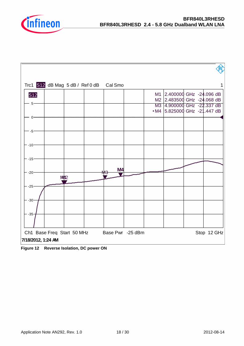
Figure 12 Reverse Isolation, DC power ON
-35
-30
-25
-20
-15
-10
-5
0
5
0
1
Base Pwr -25 dBm Ch1 Base Freq Start 50 MHz Stop 12 GHz
Trc1 S12 dB Mag 5 dB / Ref 0 dB Cal Smo
•
M1
M2
M3
M4
2.400000
2.483500
4.900000
5.825000
GHz
GHz
GHz
GHz
-24.096
-24.068
-22.337
-21.447
dB
dB
dB
dB
S12
M1M2M3
M4
7/18/2012, 1:24 AM

BFR840L3RHESD BFR840L3RHESD 2.4 - 5.8 GHz Dualband WLAN LNA
Application Note AN292, Rev. 1.0 2012-08-14 19 / 30
Figure 13 Reverse Isolation, DC Power OFF
-35
-30
-25
-20
-15
-10
-5
0
5
0
1
Base Pwr -25 dBm Ch1 Base Freq Start 50 MHz Stop 12 GHz
Trc1 S12 dB Mag 5 dB / Ref 0 dB Cal Smo
•
M1
M2
M3
M4
2.400000
2.483500
4.900000
5.825000
GHz
GHz
GHz
GHz
-19.057
-19.086
-19.010
-19.958
dB
dB
dB
dB
S12
M1M2 M3M4
7/18/2012, 1:25 AM

BFR840L3RHESD BFR840L3RHESD 2.4 - 5.8 GHz Dualband WLAN LNA
Application Note AN292, Rev. 1.0 2012-08-14 20 / 30
Note excellent output match of amplifier over entire 2.4 – 6 GHz frequency range. This eases integration with other receiver chain blocks (i.e. filters, switches, etc.)
Figure 14 Amplifier Wideband Output Return Loss
-30
-25
-20
-15
-10
-5
0
5
10
0
1
Base Pwr -25 dBm Ch1 Base Freq Start 50 MHz Stop 12 GHz
Trc1 S22 dB Mag 5 dB / Ref 0 dB Cal Smo
•
M1
M2
M3
M4
2.400000
2.483500
4.900000
5.825000
GHz
GHz
GHz
GHz
-11.068
-10.954
-12.468
-12.738
dB
dB
dB
dB
S22
M1M2M3 M4
7/18/2012, 1:26 AM

BFR840L3RHESD BFR840L3RHESD 2.4 - 5.8 GHz Dualband WLAN LNA
Application Note AN292, Rev. 1.0 2012-08-14 21 / 30
Reference Plane = SMA RF Output Connector to PC Board.
Figure 15 Amplifier Output Return Loss, Smith Chart
-5
-2
-1
-0.5
0.5
1
2
5
0 0.2 0.5 1 2 51
1
Base Pwr -25 dBm Ch1 Base Freq Start 50 MHz Stop 12 GHz
Trc1 S22 Smith Ref 1 U Cal Smo
•
M1
M2
M3
M4
2.400000
2.483500
4.900000
5.825000
GHz
GHz
GHz
GHz
33.495
j17.116
1.135
35.042
j19.804
1.269
34.234
-j12.823
2.533
35.373
j13.686
373.95
Ω
Ω
nH
Ω
Ω
nH
Ω
Ω
pF
Ω
Ω
pH
S22
M1M2
M3
M4
7/18/2012, 1:26 AM

BFR840L3RHESD BFR840L3RHESD 2.4 - 5.8 GHz Dualband WLAN LNA
Application Note AN292, Rev. 1.0 2012-08-14 22 / 30
In-Band Third Order Intercept (IIP3) Test, 2400 MHz: Input Stimulus: f1=2400 MHz, f2=2401 MHz, -28 dBm each tone Input IP3 = -28+(45.0 / 2) = - 5.5 dBm Output IP3 = - 5.5 dBm + 18.5 dB gain = +13.0 dBm
Figure 16 Amplifier Input 3rd
Order Intercept Point Measurement, 2400 MHz

BFR840L3RHESD BFR840L3RHESD 2.4 - 5.8 GHz Dualband WLAN LNA
Application Note AN292, Rev. 1.0 2012-08-14 23 / 30
Input Third Order Intercept (IIP3) Test, 5825 MHz: Input Stimulus: f1=5824 MHz, f2=5825 MHz, -28 dBm each tone Input IP3 = -28+(56.6 / 2) = +0.3 dBm Output IP3 = +0.3 dBm + 14.1 dB gain = +14.4 dBm
Figure 17 Amplifier Input 3rd
Order Intercept Point Measurement, 5825 MHz

BFR840L3RHESD BFR840L3RHESD 2.4 - 5.8 GHz Dualband WLAN LNA
Application Note AN292, Rev. 1.0 2012-08-14 24 / 30
Block Diagram, Test Setup for Amplifier Turn-On / Turn Off time measurement
Figure 18 Diagram of Setup for Making Amplifier Turn-On and Turn-Off Times.

BFR840L3RHESD BFR840L3RHESD 2.4 - 5.8 GHz Dualband WLAN LNA
Application Note AN292, Rev. 1.0 2012-08-14 25 / 30
Amplifier Turn On Time:
Refer to oscilloscope screen-shot below. Upper trace (yellow, Channel 1) is the DC power supply turn-on step waveform whereas the lower trace (green, Channel 2) is the rectified RF output signal of the LNA stage. Amplifier turn-on time is aproximately 15 nanoseconds, or ~ 0.015 microseconds. Main source of time delay in the LNA turn-on event are the R-C time constants formed by (R3 * C4), etc. Charge storage has been minimized in this circuit so as to speed up turn on and turn off times. (Refer to Schematic diagram on page X).
Figure 19 Oscilloscope Screen Shot, Amplifier Turn-On Time

BFR840L3RHESD BFR840L3RHESD 2.4 - 5.8 GHz Dualband WLAN LNA
Application Note AN292, Rev. 1.0 2012-08-14 26 / 30
Amplifier Turn-Off time
Upper trace (Channel 1, yellow color) is the falling edge of the DC power supply voltage. Rectified RF output signal (Channel 2, lower green trace) takes about ~ 15 nanoseconds, or 0.015 microseconds, to settle out after power supply is turned off.
Figure 20 Oscilloscope Screen-Shot, Amplifier Turn-Off Time

BFR840L3RHESD BFR840L3RHESD 2.4 - 5.8 GHz Dualband WLAN LNA
Application Note AN292, Rev. 1.0 2012-08-14 27 / 30
3 Evaluation Board and Layout Information
Figure 21 View of Entire PC Board

BFR840L3RHESD BFR840L3RHESD 2.4 - 5.8 GHz Dualband WLAN LNA
Application Note AN292, Rev. 1.0 2012-08-14 28 / 30
Note – five (5) 0.2mm diameter ground via holes are used for grounding (emitter connection) near top right corner of Q1. R2 is the feedback resisistor (RF Feedback).
Figure 22 Close-In View of BFR840L3RHESD Wideband / Dualband LNA.

BFR840L3RHESD BFR840L3RHESD 2.4 - 5.8 GHz Dualband WLAN LNA
Application Note AN292, Rev. 1.0 2012-08-14 29 / 30
Note – standard low-cost “FR4” PC board material is used.
BOTTOM LAYER
0.010 inch / 0.254 mm
0.031 inch / 0.787 mm ?
PCB CROSS SECTION
TOP LAYER (RF TRACES)
INTERNAL GROUND PLANE
LAYER FOR MECHANICAL RIGIDITY OF PCB, THICKNESS HERE NOT
CRITICAL AS LONG AS TOTAL PCB THICKNESS DOES NOT EXCEED
0.045 INCH / 1.14 mm (SPECIFICATION FOR TOTAL PCB THICKNESS:
0.040 + 0.005 / - 0.005 INCH; 1.016 + 0.127 mm / - 0.127 mm )
Figure 23 PC Board Cross-Section Information.
4 Author
Gerard Wevers,Senior Staff Applications Engineer of Business Unit “RF and Protection Devices”.
5 Remark
The data graphs are exported from the Rohde and Schwarz ZVB network analyzer, FS-K3 Noise Figure Measurement system, or Agilent DSO6104A Oscilloscope.

w w w . i n f i n e o n . c o m
Published by Infineon Technologies AG AN292