AN2808 Application note - STMicroelectronics · Application note Complete DDR2/3 ... buffered...
40
November 2008 Rev 1 1/40 AN2808 Application note Complete DDR2/3 memory power supply controller Introduction The PM6670S device is a complete DDR2/3 power supply regulator for portable applications designed to meet JEDEC specifications. It integrates a constant on-time (COT) buck controller, a 2 Apk sink/source low dropout regulator (LDO) and a 15 mA low noise buffered reference. The COT architecture ensures a fast transient response supporting both polymeric and ceramic output capacitors. An embedded integrator control loop compensates the DC voltage error caused by the output ripple. The 2 Apk sink/source linear regulator provides the memory termination voltage with a fast load transient response. The device is fully compliant with system sleep states S3, S4 and S5, setting the LDO output to high-impedance in the suspend-to-RAM state, and performing the tracking discharge of all outputs in the suspend-to-disk state. Figure 1. PM6670S demonstration board www.st.com
Transcript of AN2808 Application note - STMicroelectronics · Application note Complete DDR2/3 ... buffered...

November 2008 Rev 1 1/40
AN2808Application note
Complete DDR2/3 memory power supply controller
IntroductionThe PM6670S device is a complete DDR2/3 power supply regulator for portable applications designed to meet JEDEC specifications. It integrates a constant on-time (COT) buck controller, a 2 Apk sink/source low dropout regulator (LDO) and a 15 mA low noise buffered reference.
The COT architecture ensures a fast transient response supporting both polymeric and ceramic output capacitors. An embedded integrator control loop compensates the DC voltage error caused by the output ripple. The 2 Apk sink/source linear regulator provides the memory termination voltage with a fast load transient response.
The device is fully compliant with system sleep states S3, S4 and S5, setting the LDO output to high-impedance in the suspend-to-RAM state, and performing the tracking discharge of all outputs in the suspend-to-disk state.
Figure 1. PM6670S demonstration board
www.st.com
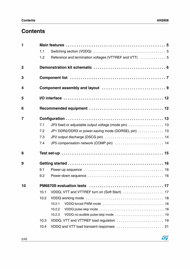
Contents AN2808
2/40
Contents
1 Main features . . . . . . . . . . . . . . . . . . . . . . . . . . . . . . . . . . . . . . . . . . . . . . . 5
1.1 Switching section (VDDQ) . . . . . . . . . . . . . . . . . . . . . . . . . . . . . . . . . . . . . 5
1.2 Reference and termination voltages (VTTREF and VTT) . . . . . . . . . . . . . 5
2 Demonstration kit schematic . . . . . . . . . . . . . . . . . . . . . . . . . . . . . . . . . . 6
3 Component list . . . . . . . . . . . . . . . . . . . . . . . . . . . . . . . . . . . . . . . . . . . . . 7
4 Component assembly and layout . . . . . . . . . . . . . . . . . . . . . . . . . . . . . . 9
5 I/O interface . . . . . . . . . . . . . . . . . . . . . . . . . . . . . . . . . . . . . . . . . . . . . . . 12
6 Recommended equipment . . . . . . . . . . . . . . . . . . . . . . . . . . . . . . . . . . . 12
7 Configuration . . . . . . . . . . . . . . . . . . . . . . . . . . . . . . . . . . . . . . . . . . . . . . 13
7.1 JP3 fixed or adjustable output voltage (mode pin) . . . . . . . . . . . . . . . . . . 13
7.2 JP1 DDR2/DDR3 or power-saving mode (DDRSEL pin) . . . . . . . . . . . . . 13
7.3 JP2 output discharge (DSCG pin) . . . . . . . . . . . . . . . . . . . . . . . . . . . . . . 14
7.4 JP5 compensation network (COMP pin) . . . . . . . . . . . . . . . . . . . . . . . . . 14
8 Test set-up . . . . . . . . . . . . . . . . . . . . . . . . . . . . . . . . . . . . . . . . . . . . . . . . 15
9 Getting started . . . . . . . . . . . . . . . . . . . . . . . . . . . . . . . . . . . . . . . . . . . . . 16
9.1 Power-up sequence . . . . . . . . . . . . . . . . . . . . . . . . . . . . . . . . . . . . . . . . . 16
9.2 Power-down sequence . . . . . . . . . . . . . . . . . . . . . . . . . . . . . . . . . . . . . . . 16
10 PM6670S evaluation tests . . . . . . . . . . . . . . . . . . . . . . . . . . . . . . . . . . . 17
10.1 VDDQ, VTT and VTTREF turn on (Soft Start) . . . . . . . . . . . . . . . . . . . . . 17
10.2 VDDQ working mode . . . . . . . . . . . . . . . . . . . . . . . . . . . . . . . . . . . . . . . . 18
10.2.1 VDDQ forced PWM mode . . . . . . . . . . . . . . . . . . . . . . . . . . . . . . . . . . . 18
10.2.2 VDDQ pulse-skip mode . . . . . . . . . . . . . . . . . . . . . . . . . . . . . . . . . . . . . 18
10.2.3 VDDQ no-audible pulse-skip mode . . . . . . . . . . . . . . . . . . . . . . . . . . . . 19
10.3 VDDQ, VTT and VTTREF load regulation . . . . . . . . . . . . . . . . . . . . . . . . 19
10.4 VDDQ and VTT load transient responses . . . . . . . . . . . . . . . . . . . . . . . . 21

AN2808 Contents
3/40
10.5 VDDQ efficiency . . . . . . . . . . . . . . . . . . . . . . . . . . . . . . . . . . . . . . . . . . . . 22
10.6 VDDQ gate drivers . . . . . . . . . . . . . . . . . . . . . . . . . . . . . . . . . . . . . . . . . . 23
10.7 VDDQ, VTT and VTTREF turn off (soft end) . . . . . . . . . . . . . . . . . . . . . . 23
10.7.1 Tracking discharge . . . . . . . . . . . . . . . . . . . . . . . . . . . . . . . . . . . . . . . . . 23
10.7.2 Non-traking discharge . . . . . . . . . . . . . . . . . . . . . . . . . . . . . . . . . . . . . . 24
10.8 UV, OV and thermal protections . . . . . . . . . . . . . . . . . . . . . . . . . . . . . . . . 25
10.8.1 Latched UV protection . . . . . . . . . . . . . . . . . . . . . . . . . . . . . . . . . . . . . . 25
10.8.2 Latched OV protection . . . . . . . . . . . . . . . . . . . . . . . . . . . . . . . . . . . . . . 25
10.9 VTT current limit (foldback) . . . . . . . . . . . . . . . . . . . . . . . . . . . . . . . . . . . 26
10.10 Switching frequency . . . . . . . . . . . . . . . . . . . . . . . . . . . . . . . . . . . . . . . . . 27
10.10.1 Switching frequency vs input voltage . . . . . . . . . . . . . . . . . . . . . . . . . . . 27
10.10.2 Switching frequency vs output current . . . . . . . . . . . . . . . . . . . . . . . . . . 27
10.11 Thermal behavior . . . . . . . . . . . . . . . . . . . . . . . . . . . . . . . . . . . . . . . . . . . 28
10.12 DDR memories (VDDQ = 2.5 V) characterization . . . . . . . . . . . . . . . . . . 32
Revision history . . . . . . . . . . . . . . . . . . . . . . . . . . . . . . . . . . . . . . . . . . . . . . . . . . . . 39

List of figures AN2808
4/40
List of figures
Figure 1. PM6670S demonstration board . . . . . . . . . . . . . . . . . . . . . . . . . . . . . . . . . . . . . . . . . . . . . . 1Figure 2. Demonstration schematic . . . . . . . . . . . . . . . . . . . . . . . . . . . . . . . . . . . . . . . . . . . . . . . . . . . 5Figure 3. Top slide component placement . . . . . . . . . . . . . . . . . . . . . . . . . . . . . . . . . . . . . . . . . . . . . 8Figure 4. Top slide view . . . . . . . . . . . . . . . . . . . . . . . . . . . . . . . . . . . . . . . . . . . . . . . . . . . . . . . . . . . 8Figure 5. Layer 2 view . . . . . . . . . . . . . . . . . . . . . . . . . . . . . . . . . . . . . . . . . . . . . . . . . . . . . . . . . . . . . 9Figure 6. Layer 3 view . . . . . . . . . . . . . . . . . . . . . . . . . . . . . . . . . . . . . . . . . . . . . . . . . . . . . . . . . . . . . 9Figure 7. Bottom side view . . . . . . . . . . . . . . . . . . . . . . . . . . . . . . . . . . . . . . . . . . . . . . . . . . . . . . . . 10Figure 8. Bottom side component placement . . . . . . . . . . . . . . . . . . . . . . . . . . . . . . . . . . . . . . . . . . 10Figure 9. JP3 (mode) setting . . . . . . . . . . . . . . . . . . . . . . . . . . . . . . . . . . . . . . . . . . . . . . . . . . . . . . . 12Figure 10. JP1 options when JP3 is in the lower position . . . . . . . . . . . . . . . . . . . . . . . . . . . . . . . . . . 13Figure 11. JP1 options when JP3 is in the upper position . . . . . . . . . . . . . . . . . . . . . . . . . . . . . . . . . . 13Figure 12. JP2 (DSCG) setting . . . . . . . . . . . . . . . . . . . . . . . . . . . . . . . . . . . . . . . . . . . . . . . . . . . . . . 13Figure 13. JP5 (COMP) setting . . . . . . . . . . . . . . . . . . . . . . . . . . . . . . . . . . . . . . . . . . . . . . . . . . . . . . 14Figure 14. PM6670S test set-up . . . . . . . . . . . . . . . . . . . . . . . . . . . . . . . . . . . . . . . . . . . . . . . . . . . . . 14Figure 15. VDDQ Soft Start @150mW load, pulse-skip mode . . . . . . . . . . . . . . . . . . . . . . . . . . . . . . 16Figure 16. VDDQ turn on (S5), pulse-skip mode . . . . . . . . . . . . . . . . . . . . . . . . . . . . . . . . . . . . . . . . 16Figure 17. VTT turn on (S0), pulse-skip mode . . . . . . . . . . . . . . . . . . . . . . . . . . . . . . . . . . . . . . . . . . 17Figure 18. VDDQ=1.8V , VIN=12V, IVDDQ=0A, forced-PWM mode. . . . . . . . . . . . . . . . . . . . . . . . . . 17Figure 19. VDDQ=1.8V, VIN=12V, IVDDQ=0.5A, pulse-skip mode . . . . . . . . . . . . . . . . . . . . . . . . . . 18Figure 20. VDDQ=1.8V, VIN=12V, no load, no-audible pulse-skip mode (33kHz) . . . . . . . . . . . . . . . 18Figure 21. VDDQ load regulation - VIN=12V, pulse-skip mode . . . . . . . . . . . . . . . . . . . . . . . . . . . . . . 19Figure 22. VTT load regulation - LDOIN=VDDQ . . . . . . . . . . . . . . . . . . . . . . . . . . . . . . . . . . . . . . . . . 19Figure 23. VTT load regulation . . . . . . . . . . . . . . . . . . . . . . . . . . . . . . . . . . . . . . . . . . . . . . . . . . . . . . 20Figure 24. VDDQ load transient (VIN=12V, LOAD=0A->8A @2.5A/ms). Pulse-skip mode. . . . . . . . . 20Figure 25. VTT load transient (VIN=12V, LOAD=-2A->2A @2.5A/ms). Pulse-skip mode. . . . . . . . . . 21Figure 26. VDDQ efficiency vs. load . . . . . . . . . . . . . . . . . . . . . . . . . . . . . . . . . . . . . . . . . . . . . . . . . . 21Figure 27. External MOSFET gate signal (VIN=12 V, load= 0 A). Pulse-skip mode . . . . . . . . . . . . . . 22Figure 28. External MOSFET gate signal (VIN=12 V, load= 8 A). Pulse-skip mode . . . . . . . . . . . . . . 22Figure 29. VDDQ, VTTREF, VTT output voltages anl LDO input current. Tracking discharge. No load on any rail . . . . . . . . . . . . . . . . . . . . . . . . . . . . . . . . . . . . . . . . . . . . . . . . . . . . . . . . . . . . . . . . . . . . . . 23Figure 30. VDDQ, VTTREF, VTT. No-tracking discharge. No load on any output. . . . . . . . . . . . . . . . 23Figure 31. UV protection, pulse-skip mode . . . . . . . . . . . . . . . . . . . . . . . . . . . . . . . . . . . . . . . . . . . . . 24Figure 32. OV protection, pulse-skip mode . . . . . . . . . . . . . . . . . . . . . . . . . . . . . . . . . . . . . . . . . . . . . 25Figure 33. VTT current limit during an output short . . . . . . . . . . . . . . . . . . . . . . . . . . . . . . . . . . . . . . . 25Figure 34. fsw vs input voltage, DDR2. . . . . . . . . . . . . . . . . . . . . . . . . . . . . . . . . . . . . . . . . . . . . . . . . 26Figure 35. fsw vs iload, Vin = 12V voltage, DDR2 . . . . . . . . . . . . . . . . . . . . . . . . . . . . . . . . . . . . . . . . 27Figure 36. VTT current vs temperature , IVTT= 0 A. . . . . . . . . . . . . . . . . . . . . . . . . . . . . . . . . . . . . . . 28Figure 37. VTT current vs temperature, IVTT= 0.5 A. . . . . . . . . . . . . . . . . . . . . . . . . . . . . . . . . . . . . . 29Figure 38. VTT current vs temperature, IVTT= 1 A . . . . . . . . . . . . . . . . . . . . . . . . . . . . . . . . . . . . . . . 30Figure 39. VTT current vs temperature, IVTT= 1.5 A. . . . . . . . . . . . . . . . . . . . . . . . . . . . . . . . . . . . . . 31Figure 40. VDDQ load regulation, Vin = 12 V and switching frequency 400 kHz . . . . . . . . . . . . . . . . 32Figure 41. VDDQ load regulation, Vin = 5 V and switching frequency 400 kHz . . . . . . . . . . . . . . . . . 32Figure 42. VTT load regulation . . . . . . . . . . . . . . . . . . . . . . . . . . . . . . . . . . . . . . . . . . . . . . . . . . . . . . 33Figure 43. VTTREF load regulation . . . . . . . . . . . . . . . . . . . . . . . . . . . . . . . . . . . . . . . . . . . . . . . . . . 33Figure 44. Efficiency vs load - VDDQ = 2.5 V, Vin = 12 V . . . . . . . . . . . . . . . . . . . . . . . . . . . . . . . . . 34Figure 45. Efficiency vs load - VDDQ = 2.5 V, Vin = 5 V . . . . . . . . . . . . . . . . . . . . . . . . . . . . . . . . . . 34Figure 46. SW efficiency vs load - VDDQ = 2.5 V, Vin = 12 V . . . . . . . . . . . . . . . . . . . . . . . . . . . . . . 35Figure 47. SW efficiency vs load - VDDQ = 2.5 V, Vin = 5 V . . . . . . . . . . . . . . . . . . . . . . . . . . . . . . . 35Figure 48. VDDQ load transient response . . . . . . . . . . . . . . . . . . . . . . . . . . . . . . . . . . . . . . . . . . . . . . 36Figure 49. VTT load transient response. . . . . . . . . . . . . . . . . . . . . . . . . . . . . . . . . . . . . . . . . . . . . . . . 36

AN2808 Main features
5/40
1 Main features
1.1 Switching section (VDDQ) 4.5 to 28-V input voltage range
0.9 V, ±1% voltage reference
1.8 V (DDR2) or 1.5 V (DDR3) fixed output voltages
0.9 to 2.6 V adjustable output voltage
1.237 V ± 1% reference voltage available
Very fast load transient response constant on-time control loop
No-RSENSE current sensing using low-side MOSFETs' RDS(on)
Negative current limit
Latched OVP, UVP and thermal shutdown
Fixed 3 ms Soft-Start
Selectable pulse-skipping at light loads
Selectable non-audible (33 kHz) pulse-skip mode
All ceramic output capacitor applications supported
Output voltage ripple compensation
1.2 Reference and termination voltages (VTTREF and VTT) 2 A peak LDO with foldback for VTT
Remote VTT output sensing
High-Z VTT output in S3
Ceramic output capacitors supported
±15 mA low-noise buffered reference for VTTREF

Demonstration kit schematic AN2808
6/40
2 Demonstration kit schematic
Figure 2. Kit schematic
00
J2 VDD
DD
Q
1
J3 PGN
D
1
J1111
AGN
D1
J1 VIN
1J5
VCC
1
JP3
MO
DE
0
0
0
U1
PM6666
70S0S
VTT2424
LDOIN2323
BOOT2222
HGATE2121
PHASASE2020
CSNS1919
VCC
1818
LGAT
E17 17
PGN
D16 16
PG15 15
S31414
S51313
DSCG1212COMP1111MODE1010VSVSNS
9VOSC8VREF7
AVAVC
C6
SGN
D5
VTTR
EF4
DD
DD
RSESE
L3
VTTS
NS
2VT
TGN
D1
THPD
25 25
J9VC
CG
ND
1
Q2
S12N
H3L
L
5
4
1678
23
Q1
S12N
H3L
L
5
4
1678
23
J1010
AGN
D1
J6
LDO
IN1
D1
BABAT5
4J54J
2 1
R4
3R3
12
0
R3
1k2
12
R1
330k30k
12
R2
18k
18k
1 2
L11u1u
12
D2
21
C1
10u0u
1 2
C2
10u0u
1 2
C3
220u
220u
1 2
C4
220u0u
1 2
C1010
1 2
C9
100n
100n
12
R7
3R9
1 2
0
C1919
10u
1 2C
131310
0n0n1
2
C2020
10u
10u
1 2
SW1
12
43
R11
10100k
12
R12
10100k
12
0
C2121
100p00p
1 2
R14
7.5k5k
R15
6.8k8k
C15
47n
47n
12
C16
68680p
12
C17
0
1 2
C6
10u0u
1 2
R17
0
VCC
VCC
VCC
VCC
C1111
10u0u
1 2
C2222
100p00
p
1 2
C8 33n
33n
1 2
C1414
100n0n
1 2
TP1
GN
D_T
P
J4 PG
1
R1313
100k00k
1 2
0
C5
1u
1 2
JP5
INT_
CER
JP2
DSC
G
123456
JP1
DD
DD
RSESE
L
123456
0
D3 ST
PSPS1L
30A
30A
21
00
C7
10u
1 2
0
0
R8
39k
39k
R9
39k
39k
R6
0
STPSPS1L3L30M
R1010
0C
121010
0n
1 2
J7VT
T1
J8
VTTR
EF1
C1818
1n
1 2
R16
4R7
0
00
AM00646v1
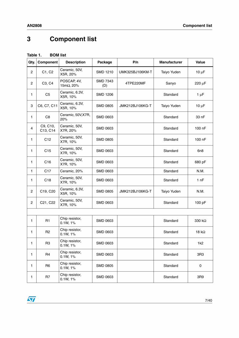
AN2808 Component list
7/40
3 Component list
Table 1. BOM list
Qty. Component Description Package P/n Manufacturer Value
2 C1, C2Ceramic, 50V, X5R, 20%
SMD 1210 UMK325BJ106KM-T Taiyo Yuden 10 µF
2 C3, C4POSCAP, 4V, 15mΩ, 20%
SMD 7343 (D)
4TPE220MF Sanyo 220 µF
1 C5Ceramic, 6.3V, X5R, 10%
SMD 1206 Standard 1 µF
3 C6, C7, C11Ceramic, 6.3V, X5R, 10%
SMD 0805 JMK212BJ106KG-T Taiyo Yuden 10 µF
1 C8Ceramic, 50V,X7R, 20%
SMD 0603 Standard 33 nF
4C9, C10, C13, C14
Ceramic, 50V, X7R, 20%
SMD 0603 Standard 100 nF
1 C12Ceramic, 50V, X7R, 10%
SMD 0805 Standard 100 nF
1 C15Ceramic, 50V, X7R, 10%
SMD 0603 Standard 6n8
1 C16Ceramic, 50V, X7R, 10%
SMD 0603 Standard 680 pF
1 C17 Ceramic, 20% SMD 0603 Standard N.M.
1 C18Ceramic, 50V, X7R, 10%
SMD 0603 Standard 1 nF
2 C19, C20Ceramic, 6.3V, X5R, 10%
SMD 0805 JMK212BJ106KG-T Taiyo Yuden N.M.
2 C21, C22Ceramic, 50V, X7R, 10%
SMD 0603 Standard 100 pF
1 R1Chip resistor, 0.1W, 1%
SMD 0603 Standard 330 kΩ
1 R2Chip resistor, 0.1W, 1%
SMD 0603 Standard 18 kΩ
1 R3Chip resistor, 0.1W, 1%
SMD 0603 Standard 1k2
1 R4Chip resistor, 0.1W, 1%
SMD 0603 Standard 3R3
1 R6Chip resistor, 0.1W, 1%
SMD 0805 Standard 0
1 R7Chip resistor, 0.1W, 1%
SMD 0603 Standard 3R9

Component list AN2808
8/40
1 R8Chip resistor, 0.1W, 1%
SMD 0603 Standard 39 kΩ
1 R9Chip resistor, 0.1W, 1%
SMD 0603 Standard 39 kΩ
1 R10Chip resistor, 0.1W, 1%
SMD 0603 Standard 0
3R11, R12,
R13Chip resistor, 0.1W, 1%
SMD 0603 Standard 100 kΩ
1 R14Chip resistor, 0.1W, 1%
SMD 0805 Standard 7k5
1 R15Chip resistor, 0.1W, 1%
SMD 0603 Standard 6k8
1 R16Chip resistor, 0.1W, 1%
SMD 0603 Standard 4R7
1 R17Chip resistor, 0.1W, 1%
SMD 0603 Standard 0
1 L1SMT, 12.4Arms, 3.46mΩ 15.0x13.2mm MLC1538-102MX Coilcraft 1 µH
1 Q1 N-channel, 30V SO-8 STS12NH3LL STMicroelectronics STS12NH3LL
1 Q2 N-channel, 30V SO-8 STS12NH3LL STMicroelectronics STS12NH3LL
1 D1 Schottky, 30V, 0.3A SOD-323 BAT54J STMicroelectronics BAT54J
1 D2 Schottky, 30V, 1AStmite
(DO216-AA)STPS1L30M STMicroelectronics STPS1L30M
1 D3 Schottky, 30V, 1AStmite
(DO216-AA)STPS1L30M STMicroelectronics N.M.
1 U1 Controller VFQFPN-24 PM6670S STMicroelectronics PM6670S
11
J1, J2, J3, J4, J5, J6, J7, J8, J9, J10,J11
Header, single pin
5JP1, JP2,
JP3Jumper, 2x3, 100mils
1 JP5 PCB pads selector
1 TP6 Test point
1 SW1 Dip switch 2 DIP-2 Standard
Table 1. BOM list (continued)
Qty. Component Description Package P/n Manufacturer Value

AN2808 Component assembly and layout
9/40
4 Component assembly and layout
Figure 3. Top side component placement
Figure 4. Top side view

Component assembly and layout AN2808
10/40
Figure 5. Layer 2 view
Figure 6. Layer 3 view
AN2808 Component assembly and layout
11/40
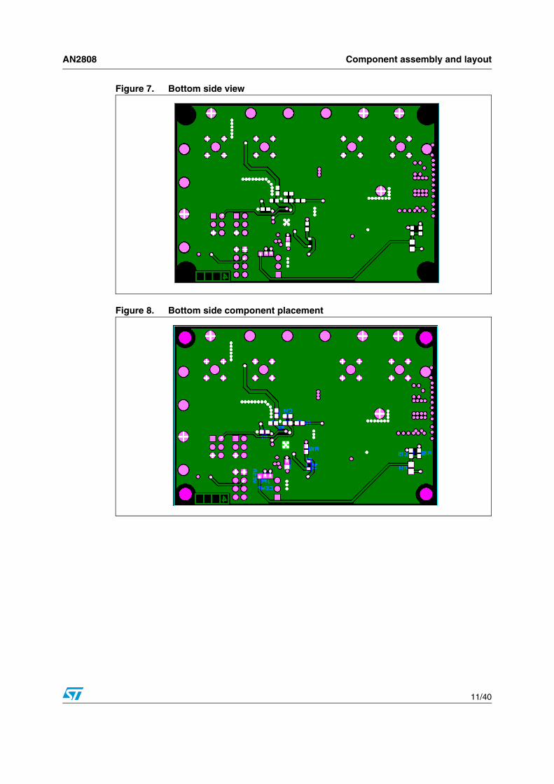
Figure 7. Bottom side view
Figure 8. Bottom side component placement

I/O interface AN2808
12/40
5 I/O interface
The PM6670S demonstration board has the following test points.
6 Recommended equipment
4 to 28-V, 30 W power supply
Active loads
Digital mutimeters
200 MHz four-trace oscilloscope
Table 2. PM6670S demonstration board input and output interface
Test point Description
VIN Battery input voltage positive terminal
PGND Battery input and VDDQ output common return
VDDQ VDDQ output
LDOIN LDO linear regulator input
VTT VTT output (LDO)
AGND VTT and VTTREF outputs common return
VTTREF VTTREF output
VCC +5 V supply, positive terminal
VCCGND Signal ground and VCC supply return
PG VDDQ output Power-Good signal
TP1 Connection point between power and signal grounds

AN2808 Configuration
13/40
7 Configuration
The PM6670S board includes four jumpers (JP1, JP2, JP3 and JP5) and two resistors, which can be configured to select the desired mode of operation.
7.1 JP3 fixed or adjustable output voltage (mode pin)The JP3 jumper is used to choose between a fixed output voltage (1.5 or 1.8 V) and a user-defined output voltage in the range of 0.9 to 2.6 V. When connected in the lower position, the fixed output voltage is selected and the voltage depends on the setting of the DDRSEL pin (Section 7.2).
If JP3 is in the upper position, the output voltage is given by:
Equation 1
Figure 9. JP3 (mode) setting
Both the R8 and R9 resistors are set to 39 kΩ (1.8 V by default) and can be changed by the user.
VDDQADJ 0.9 R8 R9+R8
----------------------⋅=

Configuration AN2808
14/40
7.2 JP1 DDR2/DDR3 or power-saving mode (DDRSEL pin)The JP1 jumper provides different options depending on the configuration of JP3. If the fixed output voltage is selected (JP3 in the lower position), the user can choose between 1.8 V (DDR2) or 1.5 V (DDR3), connecting JP1 as shown in Figure 10, and the pulse-skip mode is set by default.
When the adjustable output voltage is selected (JP3 in the upper position), the same jumper allows choosing between forced pulse width modulation (PWM), pulse-skip and non-audible pulse-skip modes.
7.3 JP2 output discharge (DSCG pin)The JP2 jumper is used to select the desired output discharge when both the S3 and S5 signals are tied low. In the upper position the outputs are not discharged at all, while in the lower position the outputs are independently discharged using the internal MOSFETs (22 Ω for VDDQ and VTT, 1.5 kΩ for VTTREF). When JP2 is in the central position, the tracking-discharge is programmed. This discharge mode relies on the LDOIN pin being connected to the VDDQ output. See Section 10.7: VDDQ, VTT and VTTREF turn-off (soft end). If an external rail is used to supply the LDO, the tracking discharge cannot be used as the device can be damaged while attempting to sink 1 A from the LDO input.
Figure 12. JP2 (DSCG) setting
Figure 10. JP1 options when JP3 is in the lower position
Figure 11. JP1 options when JP3 is in the upper position
1.5V output voltage
1.8V output voltage (default position)
1.5V output voltage
AM00647v1
No Audible Pulse-Skip
Forced PWM (default position)
Pulse-Skip
AM00648v1
Non -Tracking Discharge
No Discharge (default position)
AM00649v1

AN2808 Test setup
15/40
7.4 JP5 compensation network (COMP pin)The JP5 jumper is located on the bottom side of the PM6670S board and is used to connect the integrator input (COMP pin) to the output through a simple capacitor (integrative compensation) or using the so-called "virtual ESR" network for very low-ESR output capacitor applications (for example, all-ceramic output capacitor applications). The integrative compensation is set by default.
Refer to the PM6670S datasheet for details on all-ceramic output capacitor applications and the virtual-ESR design.
Figure 13. JP5 (COMP) setting
8 Test setup
Figure 14 shows the suggested setup connections between the PM6670S board, the loads and the external supply. The LDO input (LDOIN) is connected to VDDQ by default (R6 = 0 Ω).
Virtual ESR Network
Integrative Compensation(default position)
AM00650V1

Test setup AN2808
16/40
Figure 14. PM6670S test setup
AM00651v1

AN2808 Getting started
17/40
9 Getting started
The following step-by-step power-up and power-down sequences are provided in order to correctly evaluate the performance of the PM6670S board.
9.1 Power-up sequenceWorking in an ESD-protected environment is highly recommended. Check all wrist straps and mat earth connections before handling the PM6670S board. Connect the power supplies as shown in the PM6670S test setup (Figure 14) and insert the meters in order to perform the desired performance evaluation. Connect the scope probes as desired.
1. Set the JP1, JP2, JP3 and JP5 jumpers in order to properly configure the PM6670S board.
2. Set the S3-S5 switches to the ON (upper) position. Do not change the jumper settings when the board is powered.
3. Set the VCC supply to 5 V ± 5% and the current limit to 100 mA.
4. Set the VIN supply to a voltage in the range of 4.5 to 28 V. An initial test at 12 V and 3 A current limit is suggested.
5. Set all the loads to 0 A.
6. Turn on the VIN supply.
7. Turn on the VCC supply.
8. Vary the VDDQ load from 0 A to 10 A.
9. Vary the VTT load from 0 A to 2 A to test the source capability. To test the sink capability use the dashed VTT load shown in Figure 14.
10. Vary the VTTREF load to test the source capability.
11. Vary the VIN supply from 4.5 to 28 V.
9.2 Power-down sequence1. Decrease the VTTREF and VTT loads to 0 A.
2. Reduce the VDDQ load to 5 A.
3. Decrease the VCC supply from 5 to 3.8 V in order to test the UVLO.
4. Increase the VCC supply from 3.8 to 5 V to restart the device.
5. Use the S3-S5 switches to enter/exit the S0-S3-S5 states.
6. Turn off the VDDQ load.
7. Turn off the VCC supply.
8. Turn off the VIN supply.

PM6670S evaluation tests AN2808
18/40
10 PM6670S evaluation tests
10.1 Turning on VDDQ, VTT and VTTREF (soft-start)The VDDQ soft-start is divided into four steps. In each step, the current limit is increased by ¼ of the nominal value, as shown in Figure 15. VTT and VTTREF soft-starts are performed at their maximum available current.
Figure 15. VDDQ soft-start at 150 mΩ load, pulse-skip mode
Figure 16. VDDQ turn-on (S5), pulse-skip mode

AN2808 PM6670S evaluation tests
19/40
Figure 17. VTT turn-on (S0), pulse-skip mode
10.2 VDDQ working mode
10.2.1 VDDQ forced pulse width mode
When the forced PWM working mode is selected (JP3 and JP1 in the upper position) the inductor current is allowed to become negative and the following waveform can be captured.
Figure 18. VDDQ = 1.8 V, VIN = 12 V, IVDDQ = 0 A, forced PWM mode
10.2.2 VDDQ pulse-skip mode
The default working mode is the pulse-skip mode, in which the low-side MOSFET is turned off when the inductor current becomes equal to zero. This configuration guarantees maximum efficiency.

PM6670S evaluation tests AN2808
20/40
Figure 19. VDDQ = 1.8 V, VIN = 12 V, IVDDQ = 0.5 A, pulse-skip mode
10.2.3 VDDQ non-audible pulse-skip mode
To avoid a too low switching frequency, the non-audible pulse-skip mode can be selected (JP3 in the upper position and JP1 in the middle). The minimum switching frequency allowed is 33 kHz, as shown in Figure 20.
Figure 20. VDDQ = 1.8 V, VIN = 12 V, no load, no-audible pulse-skip mode (33 kHz)

AN2808 PM6670S evaluation tests
21/40
10.3 VDDQ, VTT and VTTREF load regulationThe following figures show the VDDQ, VTT and VTTREF output voltages against the load currents. The switching section works in pulse-skip mode and directly feeds VTT LDO.
Figure 21. VDDQ load regulation, VIN = 12 V, pulse-skip mode
Figure 22. VTT load regulation, LDOIN = VDDQ
1,800
1,802
1,804
1,806
1,808
1,810
1,812
1,814
1,816
0 1 2 3 4 5 6 7 8
Current [A]
VDD
Q [V
]
VDDQ
AM00652v1
0,870
0,880
0,890
0,900
0,910
0,920
0,930
-2,0 -1,5 -1,0 -0,5 0,0 0,5 1,0 1,5 2,0
Current [A]
VTT
[V]
VTT
AM00653v1

PM6670S evaluation tests AN2808
22/40
Figure 23. VTT load regulation
10.4 VDDQ and VTT load transient responsesTransient load responses are evaluated by loading the VDDQ and VTT output rails with a current slew rate of 2.5 A/µs.
Figure 24. VDDQ load transient (VIN = 12 V, LOAD = 0 A -> 8 A at 2.5 A/µs), pulse-skip mode
0,9
0,901
0,902
0,903
0,904
0,905
0,906
0,907
-30 -20 -10 0 10 20 30
Current [mA]
VT
TR
EF
[V]
VTTREF
AM00654v1

AN2808 PM6670S evaluation tests
23/40
Figure 25. VTT load transient (VIN = 12 V, LOAD = -2 A -> 2 A at 2.5 A/µs), pulse-skip mode
10.5 VDDQ efficiencyThe three working modes lead to different power efficiencies. The test should be setup so that VIN = 12 V, FSW = 400 kHz and VDDQ = 1.8 V. The following chart sums up the results.
Figure 26. VDDQ efficiency vs. load(a)
a. Forced PWM (yellow), no-audible pulse-skip (green), pulse-skip (blue).
0%
10%
20%
30%
40%
50%
60%
70%
80%
90%
100%
0,001 0,010 0,100 1,000 10,000
Output Current [A]
Effic
ienc
y [%
]
Forced PWM
No-Audible Pulse Skip
Pulse Skip
AM00656v1

PM6670S evaluation tests AN2808
24/40
10.6 VDDQ gate driversThe PM6670S internal MOSFET driver turns on and off the high-side and low-side external MOSFET, avoiding cross-conduction. In Figure 27 and Figure 28, the gate signals are depicted in two different load conditions: without load and with load.
Figure 27. External MOSFET gate signal (VIN = 12 V, load = 0 A),pulse-skip mode
Figure 28. External MOSFET gate signal (VIN = 12 V, load = 8 A),pulse-skip mode

AN2808 PM6670S evaluation tests
25/40
10.7 VDDQ, VTT and VTTREF turn-off (soft end)
10.7.1 Tracking discharge
The JP2 jumper, if placed in the middle, allows the output tracking to be discharged. When S3 and S5 are pulled down, VTT discharges VDDQ by sinking 1 A and, at the same time, tracks the VDDQ half. When VDDQ reaches approximately 400 mV, the output discharge MOSFETs are all closed and each rail is finally discharged.
Figure 29. VDDQ, VTTREF, VTT output voltages and LDO input current, tracking discharge, no load on any rail
10.7.2 Non-tracking discharge
When the non-tracking discharge is programmed (JP2 in the lower position) and S3-S5 are both tied to GND, each output rail is discharged through its discharge MOSFET, as depicted in Figure 30.

PM6670S evaluation tests AN2808
26/40
Figure 30. VDDQ, VTTREF, VTT – no-tracking discharge, no load on any output
10.8 UV, OV and thermal protections
10.8.1 Latched UV protection
If the output voltage is lower than the 70% nominal value, the under-voltage state is entered and the discharge MOSFETs are turned on (as in the non-tracking soft end).
Table 3. Measured discharge resistance in soft-discharge mode
VDDQ output VTTREF output VTT output
Measured N.T.D. discharge MOSFET’s RDS(on)
25Ω 1.5kΩ 23Ω

AN2808 PM6670S evaluation tests
27/40
Figure 31. UV protection, pulse-skip mode
10.8.2 Latched OV protection
If the output voltage is higher than the 115% nominal value, the over-voltage state is entered and the low-side MOSFET is turned on. VTT and VTTREF are discharged through their discharge MOSFETs.
Figure 32. OV protection, pulse-skip mode
10.9 VTT current limit (foldback)VTT LDO has a foldback protection feature which reduces the current limit to 1 A when the VTT output voltage is outside the ±10% optimum power window. The current limit is restored to 2 A when the output voltage re-enters the optimum power window.

PM6670S evaluation tests AN2808
28/40
Figure 33. VTT current limit during an output short
10.10 Switching frequency
10.10.1 Switching frequency vs input voltage
The constant on-time controller leads to a quasi-constant switching frequency, that more or less follows the input voltage.
Figure 34. fsw vs input voltage, DDR2(b)
b. Forced PWM (blue), no-audible pulse-skip (purple) and pulse-skip (yellow). Switching frequency vs input voltage, VDDQ = 1.8 V, IVDDQ = 7 A.
300
320
340
360
380
400
420
440
460
480
0 5 10 15 20 25 30
Input voltage (V)
Switc
hing
freq
uenc
y (k
Hz)
AM00659v1

AN2808 PM6670S evaluation tests
29/40
10.10.2 Switching frequency vs output current
The switching frequency can decrease to very low values in pulse-skip mode, whereas in non-audible pulse-skip there is a lower limit (about 33 kHz). With increasing loads, however, the switching frequency increases slightly as a consequence of conduction and switching losses.
Figure 35. fsw vs iload, Vin = 12 V voltage, DDR2(c)
10.11 Thermal behaviorThe IC’s internal maximum and average temperature can be monitored by an IR camera. For the following measures the test setup is:
VIN =12 V
FSW = 360 kHz
Pulse skip mode
IVDDQ = 8 A
VTT rail powered by VDDQ
TAMB = 26° C
When the VTT current is increased, the IC temperature changes as shown in the following charts.
c. Forced PWM (blue), no-audible pulse-skip (purple) and pulse-skip (yellow). Switching frequency vs output current, VDDQ = 1.8 V, no load.
0
50
100150
200
250
300
350
400
450
500
0.001 0.01 0.1 1Output current (A)
Switc
hing
freq
uenc
y (k
Hz)
AM00660v1

PM6670S evaluation tests AN2808
30/40
Figure 36. VTT current vs temperature, IVTT = 0 A(d)
d. Average IC temperature = 37.5° C. Maximum internal IC temperature = 38.8° C.

AN2808 PM6670S evaluation tests
31/40
Figure 37. VTT current vs temperature, IVTT = 0.5 A(e)
e. Average IC temperature = 46.2° C. Maximum internal IC temperature = 51.4° C.

PM6670S evaluation tests AN2808
32/40
Figure 38. VTT current vs temperature, IVTT = 1 A(f)
f. Average IC temperature = 57.4° C. Maximum internal IC temperature = 67.8° C.

AN2808 PM6670S evaluation tests
33/40
Figure 39. VTT current vs temperature, IVTT = 1.5 A(g)
10.12 DDR memories (VDDQ = 2.5 V) characterizationThe PM6670S is also suitable for DDR memories with a VDDQ rail equal to 2.5 V. The VTT linear regulator is always tracking VTTREF, a buffered replica of the VDDQ half, so the termination rail is equal to 1.25 V as required by the DDR JEDEC standards (JESD79 and JESD8-9 specifications).
The following graphs show each rail load regulation.
g. Average IC temperature = 67.9° C. Maximum internal IC temperature = 86.9° C.

PM6670S evaluation tests AN2808
34/40
Figure 40. VDDQ load regulation, Vin = 12 V and switching frequency 400 kHz
Figure 41. VDDQ load regulation, Vin = 5 V and switching frequency 400 kHz
2.460
2.470
2.480
2.490
2.500
2.510
2.520
2.530
2.540
2.550
0.001 0.010 0.100 1.000 10.000
Current [A]
Forced PWM
Pulse Skip
NO AUD. PS
Vol
tage
[V]
AM00661v1
2.460
2.470
2.480
2.490
2.500
2.510
2.520
2.530
2.540
0.001 0.010 0.100 1.000 10.000
Current [A]
Forced PWM
Pulse Skip
NO AUD. PS
Vol
tage
[V]
AM00662v1

AN2808 PM6670S evaluation tests
35/40
Figure 42. VTT load regulation (h)
Figure 43. VTTREF load regulation (h)
The efficiency of the switching section is still very high, as shown by the following graphs in which the VDDQ efficiency is computed against the load, with 12 and 5 V input voltages.
All of the three working modes (forced PWM, pulse skip and non-audible pulse skip) have been tested.
h. LDOIN = VDDQ, input voltage 5 V, switching frequency 400 kHz, forced PWM mode.
1.200
1.210
1.220
1.230
1.240
1.250
1.260
1.270
1.280
1.290
-2.0 -1.5 -1.0 -0.5 0.0 0.5 1.0 1.5 2.0
Current [A]
Vol
tag
e [V
]
AM00664v1
1.247
1.248
1.249
1.250
1.251
1.252
1.253
1.254
1.255
1.256
1.257
-30 -20 -10 0 10 20 30
Current [mA]
Vo
ltag
e [V
]
AM00665v1

PM6670S evaluation tests AN2808
36/40
Figure 44. Efficiency vs load – VDDQ = 2.5 V, Vin = 12 V
Figure 45. Efficiency vs load – VDDQ = 2.5 V, Vin = 5 V
When the input voltage is equal to 5 V the VDDQ rail efficiency is higher than 90%, with a load greater than 4 mA. This can also be achieved with a very low load when the pulse skip or non-audible pulse skip working mode is selected. The following two graphs show how the switching frequency can change with the load: by decreasing the switching frequency the regulator can greatly increase the efficiency.
0
10
20
30
40
50
60
70
80
90
100
0.001 0.010 0.100 1.000 10.000
Current [A]
Effi
cien
cy [%
]
Forced PWM
Pulse Skip
NO AUD. PS
AM00666v1
0
10
20
30
40
50
60
70
80
90
100
0.001 0.010 0.100 1.000 10.000
Current [A]
Effic
ienc
y [%
]
Forced PWMPulse SkipNO AUD. PS
AM00667v1

AN2808 PM6670S evaluation tests
37/40
Figure 46. SW efficiency vs load – VDDQ = 2.5 V, Vin = 12 V
Figure 47. SW efficiency vs load – VDDQ = 2.5 V, Vin = 5 V
The dynamic behavior of the PM6670S can be seen in the following figures, which show the VDDQ and VTT load transient response with 5 V input voltage.
0.00E+00
5.00E+04
1.00E+05
1.50E+05
2.00E+05
2.50E+05
3.00E+05
3.50E+05
4.00E+05
4.50E+05
5.00E+05
0.010 0.100 1.000 10.000
Current [A]
Fre
quen
cy [H
z]
Forced PWM
Pulse Skip
NO AUD. PS
AM00668v1
0.00E+00
5.00E+04
1.00E+05
1.50E+05
2.00E+05
2.50E+05
3.00E+05
3.50E+05
4.00E+05
4.50E+05
5.00E+05
0.010 0.100 1.000 10.000
Current [A]
Freq
uenc
y [H
z]
Forced PWM
Pulse Skip
NO AUD. PS
AM00669v1

PM6670S evaluation tests AN2808
38/40
Figure 48. VDDQ load transient response(i)
Figure 49. VTT load transient response(j)
i. The load changes from 0 to 8 A at 2.5 A/µs, input voltage 5 V, switching frequency 400 kHz, pulse skip mode.
j. The load changes from -1.5 to 1.5 A at 2.5 A/µs, input voltage 5 V, switching frequency 400 kHz, LDOIN = VDDQ pulse skip mode.

AN2808 Revision history
39/40
Revision history
Table 4. Document revision history
Date Revision Changes
14-Nov-2008 1 Initial release

AN2808
40/40
Please Read Carefully:
Information in this document is provided solely in connection with ST products. STMicroelectronics NV and its subsidiaries (“ST”) reserve theright to make changes, corrections, modifications or improvements, to this document, and the products and services described herein at anytime, without notice.
All ST products are sold pursuant to ST’s terms and conditions of sale.
Purchasers are solely responsible for the choice, selection and use of the ST products and services described herein, and ST assumes noliability whatsoever relating to the choice, selection or use of the ST products and services described herein.
No license, express or implied, by estoppel or otherwise, to any intellectual property rights is granted under this document. If any part of thisdocument refers to any third party products or services it shall not be deemed a license grant by ST for the use of such third party productsor services, or any intellectual property contained therein or considered as a warranty covering the use in any manner whatsoever of suchthird party products or services or any intellectual property contained therein.
UNLESS OTHERWISE SET FORTH IN ST’S TERMS AND CONDITIONS OF SALE ST DISCLAIMS ANY EXPRESS OR IMPLIEDWARRANTY WITH RESPECT TO THE USE AND/OR SALE OF ST PRODUCTS INCLUDING WITHOUT LIMITATION IMPLIEDWARRANTIES OF MERCHANTABILITY, FITNESS FOR A PARTICULAR PURPOSE (AND THEIR EQUIVALENTS UNDER THE LAWSOF ANY JURISDICTION), OR INFRINGEMENT OF ANY PATENT, COPYRIGHT OR OTHER INTELLECTUAL PROPERTY RIGHT.
UNLESS EXPRESSLY APPROVED IN WRITING BY AN AUTHORIZED ST REPRESENTATIVE, ST PRODUCTS ARE NOTRECOMMENDED, AUTHORIZED OR WARRANTED FOR USE IN MILITARY, AIR CRAFT, SPACE, LIFE SAVING, OR LIFE SUSTAININGAPPLICATIONS, NOR IN PRODUCTS OR SYSTEMS WHERE FAILURE OR MALFUNCTION MAY RESULT IN PERSONAL INJURY,DEATH, OR SEVERE PROPERTY OR ENVIRONMENTAL DAMAGE. ST PRODUCTS WHICH ARE NOT SPECIFIED AS "AUTOMOTIVEGRADE" MAY ONLY BE USED IN AUTOMOTIVE APPLICATIONS AT USER’S OWN RISK.
Resale of ST products with provisions different from the statements and/or technical features set forth in this document shall immediately voidany warranty granted by ST for the ST product or service described herein and shall not create or extend in any manner whatsoever, anyliability of ST.
ST and the ST logo are trademarks or registered trademarks of ST in various countries.
Information in this document supersedes and replaces all information previously supplied.
The ST logo is a registered trademark of STMicroelectronics. All other names are the property of their respective owners.
© 2008 STMicroelectronics - All rights reserved
STMicroelectronics group of companies
Australia - Belgium - Brazil - Canada - China - Czech Republic - Finland - France - Germany - Hong Kong - India - Israel - Italy - Japan - Malaysia - Malta - Morocco - Singapore - Spain - Sweden - Switzerland - United Kingdom - United States of America
www.st.com