AN1706: Microcontroller Oscillator Circuit Design Considerations
12
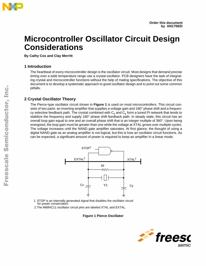
Order this document by AN1706/D Microcontroller Oscillator Circuit Design Considerations By Cathy Cox and Clay Merritt 1 Introduction The heartbeat of every microcontroller design is the oscillator circuit. Most designs that demand precise timing over a wide temperature range use a crystal oscillator. PCB designers have the task of integrat- ing crystal and microcontroller functions without the help of mating specifications. The objective of this document is to develop a systematic approach to good oscillator design and to point out some common pitfalls. 2 Crystal Oscillator Theory The Pierce-type oscillator circuit shown in Figure 1 is used on most microcontrollers. This circuit con- sists of two parts: an inverting amplifier that supplies a voltage gain and 180° phase shift and a frequen- cy selective feedback path. The crystal combined with C x and C y form a tuned PI network that tends to stabilize the frequency and supply 180° phase shift feedback path. In steady state, this circuit has an overall loop gain equal to one and an overall phase shift that is an integer multiple of 360°. Upon being energized, the loop gain must be greater than one while the voltage at XTAL grows over multiple cycles. The voltage increases until the NAND gate amplifier saturates. At first glance, the thought of using a digital NAND gate as an analog amplifier is not logical, but this is how an oscillator circuit functions. As can be expected, a significant amount of power is required to keep an amplifier in a linear mode. Figure 1 Pierce Oscillator STOP 1 Cy EXTAL 2 XTAL 2 Rf Y1 Cx 1. STOP is an internally generated signal that disables the oscillator circuit for power conservation. 2.The M68HC11 oscillator circuit pins are labeled XTAL and EXTAL. Freescale Semiconductor, I nc...
Transcript of AN1706: Microcontroller Oscillator Circuit Design Considerations
Order this document by AN1706/D
Fre
esc
ale
Se
mic
on
du
cto
r, I
nc
...
Microcontroller Oscillator Circuit Design ConsiderationsBy Cathy Cox and Clay Merritt
1 IntroductionThe heartbeat of every microcontroller design is the oscillator circuit. Most designs that demand precisetiming over a wide temperature range use a crystal oscillator. PCB designers have the task of integrat-ing crystal and microcontroller functions without the help of mating specifications. The objective of thisdocument is to develop a systematic approach to good oscillator design and to point out some commonpitfalls.
2 Crystal Oscillator TheoryThe Pierce-type oscillator circuit shown in Figure 1 is used on most microcontrollers. This circuit con-sists of two parts: an inverting amplifier that supplies a voltage gain and 180° phase shift and a frequen-cy selective feedback path. The crystal combined with Cx and Cy form a tuned PI network that tends tostabilize the frequency and supply 180° phase shift feedback path. In steady state, this circuit has anoverall loop gain equal to one and an overall phase shift that is an integer multiple of 360°. Upon beingenergized, the loop gain must be greater than one while the voltage at XTAL grows over multiple cycles.The voltage increases until the NAND gate amplifier saturates. At first glance, the thought of using adigital NAND gate as an analog amplifier is not logical, but this is how an oscillator circuit functions. Ascan be expected, a significant amount of power is required to keep an amplifier in a linear mode.
Figure 1 Pierce Oscillator
STOP1
Cy
EXTAL2 XTAL2
Rf
Y1Cx
1. STOP is an internally generated signal that disables the oscillator circuit for power conservation. 2.The M68HC11 oscillator circuit pins are labeled XTAL and EXTAL.
rxzb30
ForwardLine
rxzb30
fslcopyrightline
rxzb30
freescalecolorjpeg
Fre
esc
ale
Se
mic
on
du
cto
r, I
Freescale Semiconductor, Inc.n
c..
.
A crystal is a small wafer of high grade quartz cut at a certain angle and to a certain size. Thinner cutsgive higher frequency crystals, approximately 0.15 mm at 15 MHz. Crystals are designed and manufac-tured to operate a the rated frequency with a certain load capacitance (CL). Typical load capacitancevalues are 12 pF, 15 pF, 18 pF, 20 pF, 22 pF and 32 pF. Metal leads are plated to the crystal for elec-trical connections. As a voltage potential is placed across the crystal element, the force of trapped elec-trons in the crystalline structure tends to deform the element. This is referred to as the piezoelectriceffect. As the element flexes, electrical impedance changes. The crystal acts as an electro-mechanicaldevice and can be modeled as a network of passive electrical components with a very sharp cutoff fre-quency. The physical properties of quartz make it very stable over both time and temperature.
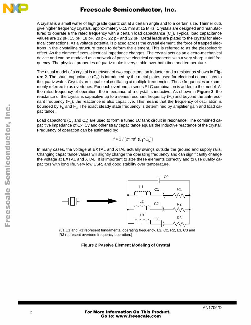
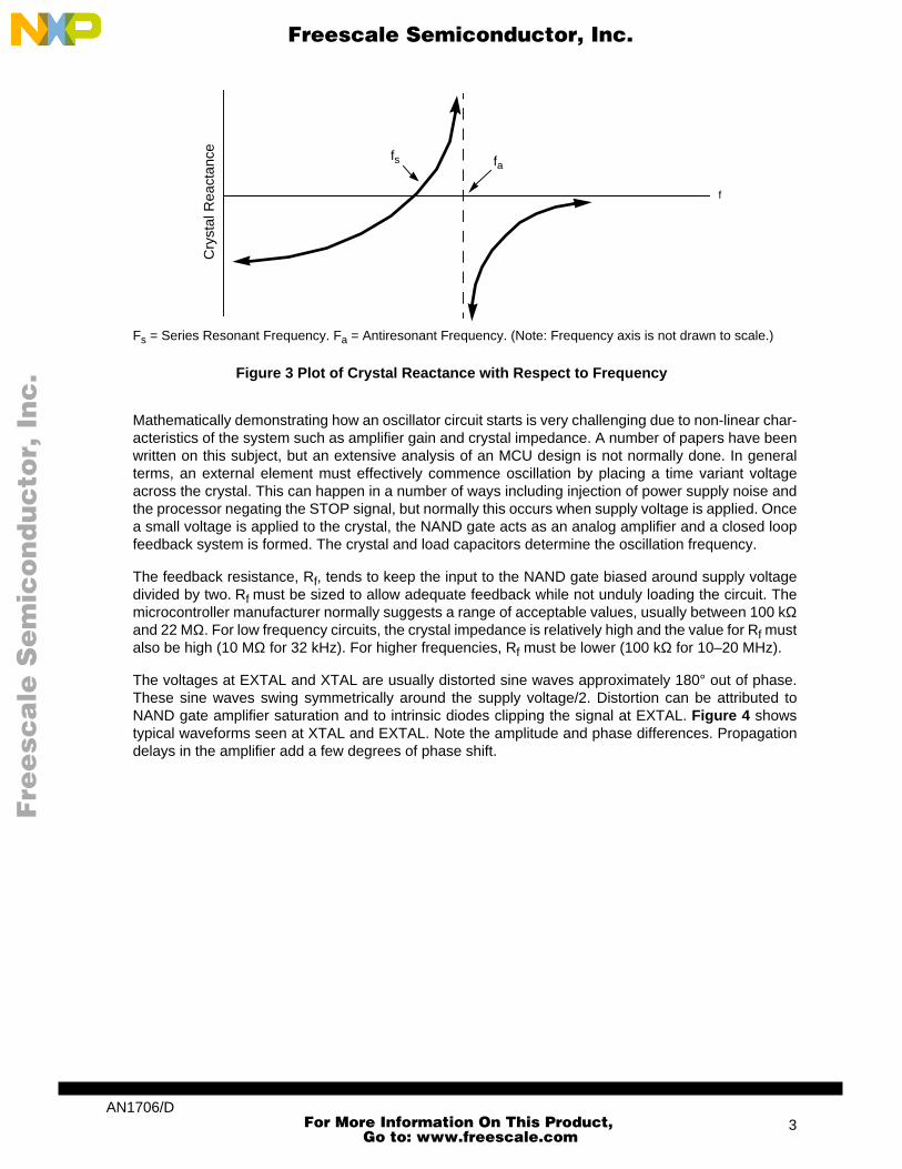
The usual model of a crystal is a network of two capacitors, an inductor and a resistor as shown in Fig-ure 2. The shunt capacitance (C0) is introduced by the metal plates used for electrical connections tothe quartz wafer. Crystals are capable of oscillating at multiple frequencies. These frequencies are com-monly referred to as overtones. For each overtone, a series RLC combination is added to the model. Atthe rated frequency of operation, the impedance of a crystal is inductive. As shown in Figure 3, thereactance of the crystal is capacitive up to a series resonant frequency (Fs) and beyond the anti-reso-nant frequency (Fa), the reactance is also capacitive. This means that the frequency of oscillation isbounded by Fs and Fa. The exact steady state frequency is determined by amplifier gain and load ca-pacitance.
Load capacitors (Cx and Cy) are used to form a tuned LC tank circuit in resonance. The combined ca-pacitive impedance of Cx, Cy and other stray capacitance equals the inductive reactance of the crystal.Frequency of operation can be estimated by:
f ≈ 1 / [2∗ π∗√ (L1∗ CL)]
In many cases, the voltage at EXTAL and XTAL actually swings outside the ground and supply rails.Changing capacitance values will slightly change the operating frequency and can significantly changethe voltage at EXTAL and XTAL. It is important to size these elements correctly and to use quality ca-pacitors with long life, very low ESR, and good stability over temperature.
(L1,C1 and R1 represent fundamental operating frequency. L2, C2, R2, L3, C3 andR3 represent overtone frequency operation.)
Figure 2 Passive Element Modeling of Crystal
C0
L1
L2
L3
C1
C2
C3
R1
R2
R3
AN1706/D2
For More Information On This Product,
Go to: www.freescale.com
F
ree
sca
le S
em
ico
nd
uc
tor,
I
Freescale Semiconductor, Inc.n
c..
.
Fs = Series Resonant Frequency. Fa = Antiresonant Frequency. (Note: Frequency axis is not drawn to scale.)
Figure 3 Plot of Crystal Reactance with Respect to Frequency
Mathematically demonstrating how an oscillator circuit starts is very challenging due to non-linear char-acteristics of the system such as amplifier gain and crystal impedance. A number of papers have beenwritten on this subject, but an extensive analysis of an MCU design is not normally done. In generalterms, an external element must effectively commence oscillation by placing a time variant voltageacross the crystal. This can happen in a number of ways including injection of power supply noise andthe processor negating the STOP signal, but normally this occurs when supply voltage is applied. Oncea small voltage is applied to the crystal, the NAND gate acts as an analog amplifier and a closed loopfeedback system is formed. The crystal and load capacitors determine the oscillation frequency.
The feedback resistance, Rf, tends to keep the input to the NAND gate biased around supply voltagedivided by two. Rf must be sized to allow adequate feedback while not unduly loading the circuit. Themicrocontroller manufacturer normally suggests a range of acceptable values, usually between 100 kΩand 22 MΩ. For low frequency circuits, the crystal impedance is relatively high and the value for Rf mustalso be high (10 MΩ for 32 kHz). For higher frequencies, Rf must be lower (100 kΩ for 10–20 MHz).
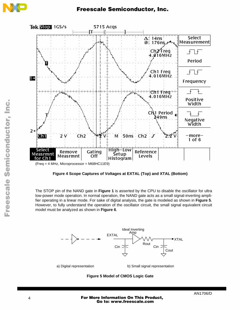
The voltages at EXTAL and XTAL are usually distorted sine waves approximately 180° out of phase.These sine waves swing symmetrically around the supply voltage/2. Distortion can be attributed toNAND gate amplifier saturation and to intrinsic diodes clipping the signal at EXTAL. Figure 4 showstypical waveforms seen at XTAL and EXTAL. Note the amplitude and phase differences. Propagationdelays in the amplifier add a few degrees of phase shift.
fa
fC
ryst
al R
eact
ance fs
AN1706/D 3
For More Information On This Product,
Go to: www.freescale.com
Fre
esc
ale
Se
mic
on
du
cto
r, I
Freescale Semiconductor, Inc.n
c..
.
(Freq = 4 MHz, Microprocessor = M68HC11E9)
Figure 4 Scope Captures of Voltages at EXTAL (Top) and XTAL (Bottom)
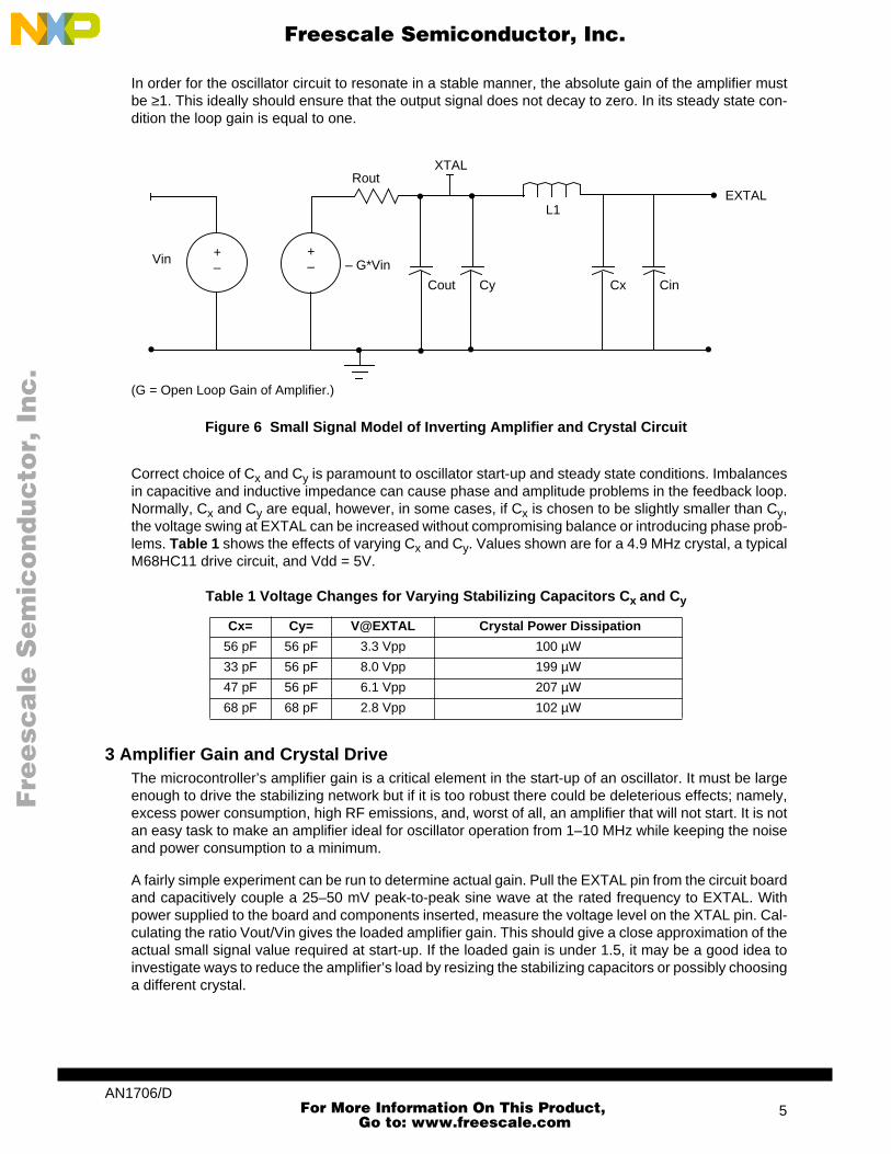
The STOP pin of the NAND gate in Figure 1 is asserted by the CPU to disable the oscillator for ultralow-power mode operation. In normal operation, the NAND gate acts as a small signal-inverting ampli-fier operating in a linear mode. For sake of digital analysis, the gate is modeled as shown in Figure 5.However, to fully understand the operation of the oscillator circuit, the small signal equivalent circuitmodel must be analyzed as shown in Figure 6.
a) Digital representation b) Small signal representation
Figure 5 Model of CMOS Logic Gate
Rout
Cout
EXTAL
Cin
XTAL
Ideal InvertingAmp
Cin
AN1706/D4
For More Information On This Product,
Go to: www.freescale.com
Fre
esc
ale
Se
mic
on
du
cto
r, I
Freescale Semiconductor, Inc.n
c..
.
In order for the oscillator circuit to resonate in a stable manner, the absolute gain of the amplifier mustbe ≥1. This ideally should ensure that the output signal does not decay to zero. In its steady state con-dition the loop gain is equal to one.
(G = Open Loop Gain of Amplifier.)
Figure 6 Small Signal Model of Inverting Amplifier and Crystal Circuit
Correct choice of Cx and Cy is paramount to oscillator start-up and steady state conditions. Imbalancesin capacitive and inductive impedance can cause phase and amplitude problems in the feedback loop.Normally, Cx and Cy are equal, however, in some cases, if Cx is chosen to be slightly smaller than Cy,the voltage swing at EXTAL can be increased without compromising balance or introducing phase prob-lems. Table 1 shows the effects of varying Cx and Cy. Values shown are for a 4.9 MHz crystal, a typicalM68HC11 drive circuit, and Vdd = 5V.
3 Amplifier Gain and Crystal DriveThe microcontroller’s amplifier gain is a critical element in the start-up of an oscillator. It must be largeenough to drive the stabilizing network but if it is too robust there could be deleterious effects; namely,excess power consumption, high RF emissions, and, worst of all, an amplifier that will not start. It is notan easy task to make an amplifier ideal for oscillator operation from 1–10 MHz while keeping the noiseand power consumption to a minimum.
A fairly simple experiment can be run to determine actual gain. Pull the EXTAL pin from the circuit boardand capacitively couple a 25–50 mV peak-to-peak sine wave at the rated frequency to EXTAL. Withpower supplied to the board and components inserted, measure the voltage level on the XTAL pin. Cal-culating the ratio Vout/Vin gives the loaded amplifier gain. This should give a close approximation of theactual small signal value required at start-up. If the loaded gain is under 1.5, it may be a good idea toinvestigate ways to reduce the amplifier’s load by resizing the stabilizing capacitors or possibly choosinga different crystal.
Table 1 Voltage Changes for Varying Stabilizing Capacitors Cx and Cy
Cx= Cy= V@EXTAL Crystal Power Dissipation
56 pF 56 pF 3.3 Vpp 100 µW
33 pF 56 pF 8.0 Vpp 199 µW
47 pF 56 pF 6.1 Vpp 207 µW
68 pF 68 pF 2.8 Vpp 102 µW
Vin +–
+–
Rout
– G*Vin
Cout Cy
XTAL
EXTALL1
Cx Cin
AN1706/D 5
For More Information On This Product,
Go to: www.freescale.com
Fre
esc
ale
Se
mic
on
du
cto
r, I
Freescale Semiconductor, Inc.n
c..
.
Overdriving a crystal for an extended period of time can physically damage a crystal. Typical drive levelsfor crystals can vary from 1 µW (for small 32 kHz tuning fork crystals) to 5 mW (for a circular AT-cut typehigh frequency crystals). By calculating the RMS current flowing through the circuit and being given themaximum series resistance, the power can be calculated using the formula:
P = I2R.
3.1 Understanding Capacitive Coupling and Inductance of PCB Traces
As PCB and semiconductor geometries get progressively smaller, the understanding and control of ca-pacitive coupling becomes paramount. Capacitance for two parallel plates can be calculated using thefollowing formula:
C (farads) = k ε0 (A / d).
Where:
ε0 = Permitivity of Free space = 8.85 * 1012 Coulombs2/Newton * Meter2
A = Plate area
d = Distance between plates
k = Dielectric constant of material
3.1.1 Example:
Consider a trace 1.0 cm long by 0.1 cm wide sitting directly above a solid ground plane. The board is atwo-layer FR4 type with a distance between copper layers being 0.031 cm. The dielectric constant offiberglass is approximately 3.5.
C = 3.5 * 8.85*10-12 * (.01m*.001m)/.00031m = 1 10-12 F or 1 pF.
With surface-mount devices, the pad area for components can actually increase and for multilayerboards the distance (d) can be very small. These factors can increase the board’s stray capacitancevalues into 5–10 pF range quite easily. For hybrid printed circuit boards, a very thin dielectric isscreened between conducting layers. This can sometimes make the distance between layers 1–2 mils( 2.5–5 mm). The dielectric constant can be between 10–15, giving stray capacitance values between15–50 pF for even nominal pad and trace sizes.
In regard to inductance, when current flows through any conductor there is some associated self induc-tance. The measured inductance is dependent on the current loop area. Having a large ground planecan usually guarantee the smallest loop area. Users of single layer boards and two layer boards withoutground planes must take special precautions to keep the oscillator trace length as short as possible andwith minimal loop area. Care should be taken to ensure the power source to the microcontroller is welldecoupled.
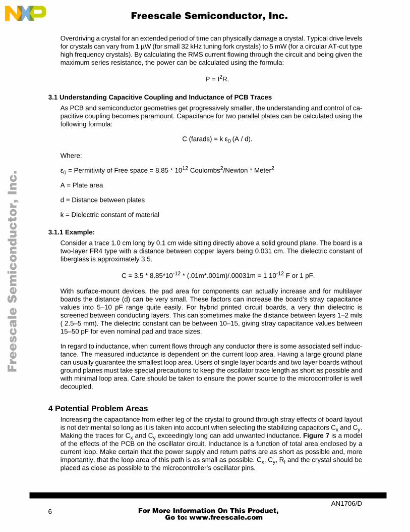
4 Potential Problem AreasIncreasing the capacitance from either leg of the crystal to ground through stray effects of board layoutis not detrimental so long as it is taken into account when selecting the stabilizing capacitors Cx and Cy.Making the traces for Cx and Cy exceedingly long can add unwanted inductance. Figure 7 is a modelof the effects of the PCB on the oscillator circuit. Inductance is a function of total area enclosed by acurrent loop. Make certain that the power supply and return paths are as short as possible and, moreimportantly, that the loop area of this path is as small as possible. Cx, Cy, Rf and the crystal should beplaced as close as possible to the microcontroller’s oscillator pins.
AN1706/D6
For More Information On This Product,
Go to: www.freescale.com
Fre
esc
ale
Se
mic
on
du
cto
r, I
Freescale Semiconductor, Inc.n
c..
.
Figure 7 Modeling of PCB Effects on Oscillator Circuit
The following problems have been witnessed by Freescale application engineers:
• Long trace leads: — Long trace leads and uncontrolled capacitive coupling can cause problems. Referring to Fig-
ure 7, if L1 or L2 are any significant level, the net impedance of the Cx+Lx or Cy+Ly can be verysmall, effectively eliminating any feedback voltage. If there is any significant capacitance, theeffective loading of the amplifier may be much more than calculated and the gain may not besufficient. This is probably the number one problem encountered. Multilayer and hybrid PCBscan have substantial coupling to ground. See 5 Testing and Troubleshooting for more onthis problem.
• PCB contaminants: — PCB contaminants reducing impedance between nodes such as humidity, flux, and finger
prints are problems. When printed circuit boards are manufactured, a flux is applied to theboard to promote good solder bonds. Normally, a wash cycle is used to remove the flux. If theboard is not cleaned entirely, the residual flux may supply an unwanted impedance path on theboard. Take special care to check between the crystal leads and beneath SMT devices. Theseare notorious locations for flux build-up. Humidity or actual condensation on the board can alsosupply unwanted impedance paths. Referring to Figure 6 if Rx2 is introduced due to contam-inants, the input offset voltage will be pulled towards ground. This will effectively lower the am-plifiers gain by limiting the input voltage swing.
• Power supply noise: — Power supply noise can sometimes be greatly amplified by the oscillator’s amplifier. If the pow-
er supply noise is some harmonic of the crystal frequency, or vice versa, the oscillator may notbegin to oscillate. In other cases, it has been seen that a noise element on the power supplyactually helped the circuit begin oscillating by supplying a much needed high frequency com-ponent. Tying the stabilizing capacitors to +5 V sometimes provides a better AC referencepoint than ground. A good test for this condition is to disable the board’s power supply and usea high-quality bench supply to power the board. If the oscillator starts with the bench supplybut not with the board supply, look at cleaning up the +5 V rail. In most cases, if power supplynoise is a problem, the voltage at XTAL will be a constant around V supply/2.
• No operation at high temperature: — The crystal may not start at high temperatures. Usually this is caused by undue loading of the
amplifier. Check on-board contaminants and the proper sizing of the stabilizing capacitors.
+5V
Rx1
Rx2
Cx
Lx
EXTAL
Rf
XTAL
+5V
Ry1
Ry2
Cy
Ly
AN1706/D 7
For More Information On This Product,
Go to: www.freescale.com
F
ree
sca
le S
em
ico
nd
uc
tor,
I
Freescale Semiconductor, Inc.n
c..
.
• Frequency instability: — Frequency instability is usually caused either by driving the crystal too hard or insufficiently due
to incorrectly sized stabilizing capacitors. If prolonged, overdriving the crystal can cause per-manent damage. See 3 Amplifier Gain and Crystal Drive for details on the drive level of thecrystal. It should be noted that the size of the stabilizing capacitors controls the voltage acrossthe crystal.
• High frequency issues (>10 MHz): — A CMOS amplifier tends to have a gain attenuation as frequency increases. In most microcon-
trollers, the open loop gain of the amplifier is sufficiently above one at the maximum operatingfrequency to ensure good performance. However, feeding auxiliary microprocessors or otherdigital circuits can add sufficient load to swamp the amplifier and prevent oscillation. Also notethat as the frequency becomes very large, the impedance of a capacitor decreases which canmake stray capacitance a much greater problem.
• Low frequency issues (<50 kHz): — At low frequencies the capacitor and crystal impedances are very high and quite often the am-
plifier is too robust for safe operation. By placing a large resistance in series with the crystal,power dissipation can be reduced. See APPENDIX C 32-kHz Operation Specifics for properplacement of this resistor and more on low frequencies.
• Evaluation board problems:— Introducing a cable to connect a development platform to a target system can greatly change
circuit parameters. In most applications, it is better to use the oscillator circuit on the evaluationto eliminate the transmission line effects of a long cable leading to the target board. If a differ-ent frequency is required, try changing the crystal on the evaluation board. (Note: check forpossible limitations of baud rate when changing crystals in evaluation boards.)
• High-power circuit interference:— Rapidly varying high current or high voltage lines in the vicinity of the crystal circuit can ad-
versely impact the oscillator. A single error may cause the address or data bus to be misreadand software confusion can occur. If a product seems to be working correctly until a heavy loadlike a relay or motor is energized, coupling is probably occurring. Check that the decouplingcapacitors of the microcontroller are not damaged and are of high quality. Take care to routeall power traces as far away from the crystal circuit as can be allowed and keep the loop areaof all power traces to a minimum. If the ground plane has noise due to high current pulses, trytying the stabilizing capacitors to +5V instead of ground.
• EPROM to ROM differences: — Sometimes EPROM devices function correctly but ROM devices do not; or different genera-
tions of the same family function differently. As parts are shrunk to lower geometries, the am-plifier gain characteristics are sometimes changed. In some cases the EPROM and ROMdevices are in different geometries. In most cases, re-sizing the stabilizing capacitors will solvethis problem. Lowering the value of Cx while keeping CL constant will increase the voltage atEXTAL. (Note: When a part is shrunk, customers are sent product change notices (PCNs).)
• Crystal or Resonator Damage: — In rare cases, the hermetic seal on crystal leads can be fractured. This can allow moisture or
other contaminants to infiltrate the case and cause sporadic operation. Care should be takenwhen handling crystals and when forming leads prior to insertion onto a PCB. In applicationswhere the printed circuit board will be subjected to vibration, it is highly recommended that can-type crystals be adhered to the board. This will limit the stress and strain applied to the actualleads. Many crystals have been damaged when the large can case of a crystal is used as aconvenient handle to pick up and carry PCBs. This is another reason to either use smaller crys-tals or to adhere the case to the PCB.
5 Testing and TroubleshootingThe oscillator circuit is inherently a very high-impedance, closed-loop feedback system. When a stan-dard oscilloscope probe is connected into the circuit, parameters and performance can change dramat-ically. This section suggests techniques for measuring the circuit in ways that will not affect it assignificantly as a standard oscilloscope probe.
AN1706/D8
For More Information On This Product,
Go to: www.freescale.com
F
ree
sca
le S
em
ico
nd
uc
tor,
I
Freescale Semiconductor, Inc.n
c..
.
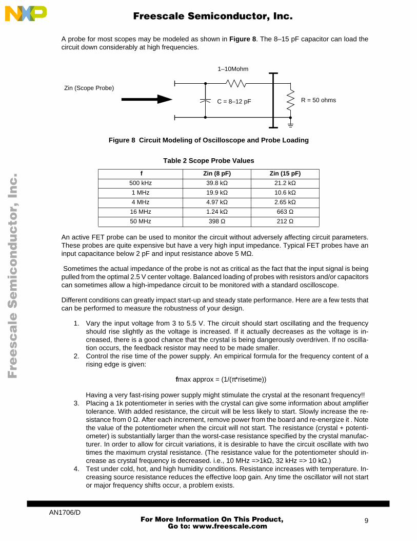
A probe for most scopes may be modeled as shown in Figure 8. The 8–15 pF capacitor can load thecircuit down considerably at high frequencies.
Figure 8 Circuit Modeling of Oscilloscope and Probe Loading
An active FET probe can be used to monitor the circuit without adversely affecting circuit parameters.These probes are quite expensive but have a very high input impedance. Typical FET probes have aninput capacitance below 2 pF and input resistance above 5 MΩ.
Sometimes the actual impedance of the probe is not as critical as the fact that the input signal is beingpulled from the optimal 2.5 V center voltage. Balanced loading of probes with resistors and/or capacitorscan sometimes allow a high-impedance circuit to be monitored with a standard oscilloscope.
Different conditions can greatly impact start-up and steady state performance. Here are a few tests thatcan be performed to measure the robustness of your design.
1. Vary the input voltage from 3 to 5.5 V. The circuit should start oscillating and the frequencyshould rise slightly as the voltage is increased. If it actually decreases as the voltage is in-creased, there is a good chance that the crystal is being dangerously overdriven. If no oscilla-tion occurs, the feedback resistor may need to be made smaller.
2. Control the rise time of the power supply. An empirical formula for the frequency content of arising edge is given:
fmax approx = (1/(π*risetime))
Having a very fast-rising power supply might stimulate the crystal at the resonant frequency!!3. Placing a 1k potentiometer in series with the crystal can give some information about amplifier
tolerance. With added resistance, the circuit will be less likely to start. Slowly increase the re-sistance from 0 Ω. After each increment, remove power from the board and re-energize it . Notethe value of the potentiometer when the circuit will not start. The resistance (crystal + potenti-ometer) is substantially larger than the worst-case resistance specified by the crystal manufac-turer. In order to allow for circuit variations, it is desirable to have the circuit oscillate with twotimes the maximum crystal resistance. (The resistance value for the potentiometer should in-crease as crystal frequency is decreased. i.e., 10 MHz =>1kΩ, 32 kHz => 10 kΩ.)
4. Test under cold, hot, and high humidity conditions. Resistance increases with temperature. In-creasing source resistance reduces the effective loop gain. Any time the oscillator will not startor major frequency shifts occur, a problem exists.
Table 2 Scope Probe Values
f Zin (8 pF) Zin (15 pF)
500 kHz 39.8 kΩ 21.2 kΩ 1 MHz 19.9 kΩ 10.6 kΩ4 MHz 4.97 kΩ 2.65 kΩ
16 MHz 1.24 kΩ 663 Ω50 MHz 398 Ω 212 Ω
Zin (Scope Probe)
1–10Mohm
R = 50 ohmsC = 8–12 pF
AN1706/D 9
For More Information On This Product,
Go to: www.freescale.com
F
ree
sca
le S
em
ico
nd
uc
tor,
I
Freescale Semiconductor, Inc.n
c..
.
5. Run worst-case loading conditions on the power portion of the board. Drive inductive loadssuch as relays, solenoids and motors under full load conditions. In certain circumstances, themagnetic field or the electric field can couple into the relatively high impedance oscillator caus-ing transients. This can sometimes be detected by the microprocessor’s software running intoconfusion due to a very short clock pulse not being properly recognized by the CPU.
6. Check board capacitance using this test. Measure the exact frequency of the crystal with atightly controlled load capacitance on a separate apparatus. Then, measure the frequency onthe actual PCB. If the two do not correlate well, unknown stray capacitance may exist on theboard and the stabilizing capacitors may need to be reduced.
One last note, if the circuit does not commence oscillating when the circuit is energized, check the volt-ages at EXTAL and XTAL. If one is high and one is low, stray impedances are probably present causingunwanted coupling between crystal leads, either to ground or to the power rail. If the voltage at EXTALis a +2.5 VDC, the feedback resistor is insufficient or a severe noise element is present on the poweror ground rails.
6 ConclusionsThis document has given a basic explanation of how and why a crystal oscillator circuit operates. Sug-gestions have been given on how to size circuit components, and how to test the circuit’s robustness.Some of the design and implementation problems experienced by Freescale application engineers havebeen discussed in the hope of preventing similar problems from occurring in the future.
Many assumptions about modeling have been made in the analysis of oscillator circuits. Most of theassumptions have been empirically proven but this document does not attempt to stringently performmathematical derivations. Many of the circuit elements change non-linearly over frequency, loading,and temperature (i.e., crystal impedance and amplifier gain) making precise modeling a non-trivial task.
7 References1. Burch, Ken, XTAL. 1992 2. KDS America, KDS Crystal Catalog. 19953. Van Doren, Dr. Tom, Grounding and Shielding Electronic Systems.4. VX Kyocera, Timing Devices.5. Sears, Francis, University Physics. 1982.6. Landee, Robert, Electronics Designers’ Handbook. McGraw-Hill, 19777. Frerking, Marvin, Crystal Oscillator Design and Temperature Compensation. Van Nostrand
Reinhold, 1978.8. Freescale Component Product Division, Product Catalog. 1994.9. Fox Electronics, Frequency Control Products. Volume 15 Number 1994.
APPENDIX A Crystal Versus Resonator IssuesResonators are a lower-cost, less exact alternative to crystals. Instead of a quartz crystal element, res-onators make use of other piezoelectric crystalline structures such as barium titanate. This allows theelement to be smaller, less expensive, and to have improved start-up times. The surrounding circuitryis identical to that of a crystal with a parallel resistor to help in the start-up phase and with stabilizingcapacitors on both legs to ground (see Figure 1).
For a given frequency, the required stabilizing capacitors are usually much larger for a resonator. Thismeans that a slightly larger amplifier drive capability is needed which will tend to consume more power.
Resonators in general are not offered below 125 kHz but are available up to 20 MHz.
AN1706/D10
For More Information On This Product,
Go to: www.freescale.com
F
ree
sca
le S
em
ico
nd
uc
tor,
I
Freescale Semiconductor, Inc.n
c..
.
APPENDIX B AT-Strip Crystals.The “AT” in AT-cut and AT-strip crystals specifies the angle of cut relative to the Z-axis to be 35 degrees.AT-cut crystals are thin, circular disks of quartz while AT-strip crystals are thin, rectangular pieces ofquartz (the width is very small compared to the length). AT-cut crystals will fit in smaller packages andrequire less quartz which should make them less expensive.
AT-strip crystals function identically to the AT-cut type and the same Pierce oscillator circuit configura-tion is used. However, the smaller piece of quartz is not as resistant to mechanical shock or to excesselectrical drive. Care should be taken to calculate the drive level and ensure stabilizing capacitorsare sized appropriately. In general, for any given frequency, the series resistance and the maximumdrive of an AT-strip crystal will be lower than that of an AT-cut crystal. (i.e., 4 MHz AT-cut: max ESR =120 Ω, max drive = 5 mW; 4 MHz AT-strip: max ESR = 40 Ω, max drive = 1 mW)
The M68HC11 reference manual contains a statement warning against the use of AT-strip type crystals.This statement was made when AT-strip crystals were just being developed and the drive level wasthought to be much lower than those specified today. There are many successful designs in productionusing AT-strip crystals with M68HC11’s. Designers should not be inhibited from using either a ceramicresonator, AT-strip, or AT-cut crystals in their microcontroller application.
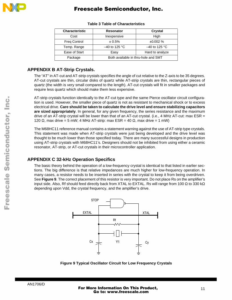
APPENDIX C 32-kHz Operation SpecificsThe basic theory behind the operation of a low-frequency crystal is identical to that listed in earlier sec-tions. The big difference is that relative impedances are much higher for low-frequency operation. Inmany cases, a resistor needs to be inserted in series with the crystal to keep it from being overdriven.See Figure 9. The correct placement of this resistor is very important. Do not place Rs on the amplifier’sinput side. Also, Rf should feed directly back from XTAL to EXTAL. Rs will range from 100 Ω to 330 kΩdepending upon Vdd, the crystal frequency, and the amplifier’s drive.
Figure 9 Typical Oscillator Circuit for Low Frequency Crystals
Table 3 Table of Characteristics
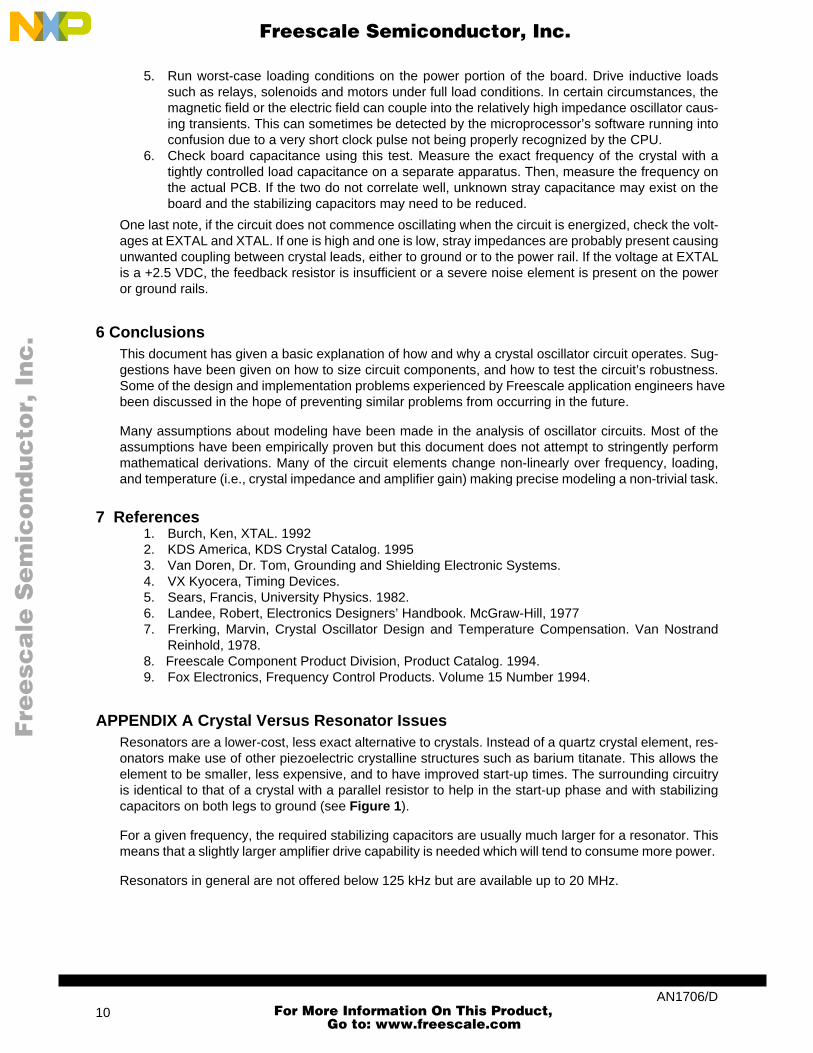
Characteristic Resonator Crystal
Cost Inexpensive High
Freq Control ± 0.5% ±0.002 %
Temp. Range –40 to 125 °C –40 to 125 °C
Ease of Start Easy Hard to analyze
Package Both available in thru-hole and SMT
STOP
Cy
EXTAL XTAL
Rf
Y1Cx
AN1706/D 11
For More Information On This Product,
Go to: www.freescale.com
e
F
ree
sca
le S
em
ico
nd
uc
tor,
I
Freescale Semiconductor, Inc.n
c..
.
Phase-locked loops are control circuits that depend upon negative feedback for stability. This meansthat the output frequency will always contain small deviations from the desired frequency. In most Freescale microcontrollers using PLLs, separate power and ground pins are supplied for the PLL. Thespins need a separate high-quality decoupling capacitor to eliminate any noise for this very sensitive cir-cuit. Even more important is a pin labeled “XFC.” This is for connection of a high-quality 0.1 µF capacitorto act as a filter in the PLL’s feedback. If nothing is connected, or a capacitor with a high ESR is used,the PLL probably will not lock.
For microprocessors utilizing phase-locked loops (PLLs), a parameter called “jitter” needs to be speci-fied. Jitter, or clock stability, is defined as the variance in maximum frequency over a specified time pe-riod. For a 16.7-MHz system, jitter can vary by up to 100 kHz for any given five microsecond window.However, over a longer window of time, say one millisecond, the average frequency can be controlledto +/– 0.05%. Variation of crystal frequency would also need to be included in the timer system absoluteerror.
rxzb30
disclaimer
rxzb30
hibbertleft
rxzb30
hibbertleft
rxzb30
freescalecolorjpeg