AN137 TOPLED® E1608 LEDs for automotive interior design · A. LEDs for automotive interior design...
13
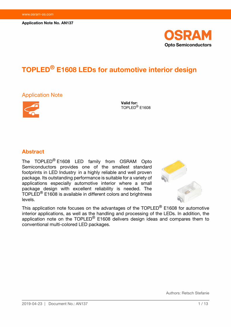
1 / 13 2019-04-23 | Document No.: AN137 www.osram-os.com Application Note TOPLED ® E1608 LEDs for automotive interior design Abstract The TOPLED ® E1608 LED family from OSRAM Opto Semiconductors provides one of the smallest standard footprints in LED Industry in a highly reliable and well proven package. Its outstanding performance is suitable for a variety of applications especially automotive interior where a small package design with excellent reliability is needed. The TOPLED ® E1608 is available in different colors and brightness levels. This application note focuses on the advantages of the TOPLED ® E1608 for automotive interior applications, as well as the handling and processing of the LEDs. In addition, the application note on the TOPLED ® E1608 delivers design ideas and compares them to conventional multi-colored LED packages. Valid for: TOPLED ® E1608 Authors: Retsch Stefanie Application Note No. AN137
Transcript of AN137 TOPLED® E1608 LEDs for automotive interior design · A. LEDs for automotive interior design...
1 / 132019-04-23 | Document No.: AN137
www.osram-os.com
Application Note
TOPLED® E1608 LEDs for automotive interior design
Abstract
The TOPLED® E1608 LED family from OSRAM OptoSemiconductors provides one of the smallest standardfootprints in LED Industry in a highly reliable and well provenpackage. Its outstanding performance is suitable for a variety ofapplications especially automotive interior where a smallpackage design with excellent reliability is needed. TheTOPLED® E1608 is available in different colors and brightnesslevels.
This application note focuses on the advantages of the TOPLED® E1608 for automotiveinterior applications, as well as the handling and processing of the LEDs. In addition, theapplication note on the TOPLED® E1608 delivers design ideas and compares them toconventional multi-colored LED packages.
Valid for:TOPLED® E1608
Authors: Retsch Stefanie
Application Note No. AN137

www.osram-os.com
Table of contents
A. LEDs for automotive interior design ........................................................................2
B. TOPLED® E1608 LED family ..................................................................................3
LED product portfolio .........................................................................................4
Comparison to other packages ..........................................................................4
C. Handling ..................................................................................................................4
ESD stability ........................................................................................................5
Precaution and storage ......................................................................................5
Cleaning ..............................................................................................................5
Manual handling .................................................................................................6
D. Processing ..............................................................................................................6
Pick-and-place nozzle design .............................................................................6
Solder pad design ...............................................................................................7
Assembly process ..............................................................................................7
Solder quality ......................................................................................................8
E. Automotive applications ........................................................................................10
Thin profile designs, thin lightguides ................................................................10
Dual color applications .....................................................................................11
Flexible multi-color applications .......................................................................11
F. Summary ...............................................................................................................12
A. LEDs for automotive interior design
The automotive interior is evolving from a function oriented design into a secondliving room away from home. This is mainly driven by the trend towardsautonomous vehicles, where comfort, safety, and awareness are important.Lighting is one key element in optimizing visual communication with the driverand enhancing the comfort for all passengers during their journey.
However, not all current lighting solutions are suitable to meet these upcomingrequirements. As lighting becomes more complex, individual light sources mustbecome smaller to allow for more strategic light placement and more color
2 / 132019-04-23 | Document No.: AN137
www.osram-os.com
flexibility. Thus, the market has pushed optoelectronic manufacturers to deliverbrighter and smaller LEDs for the automotive interior industry.
B. TOPLED® E1608 LED family
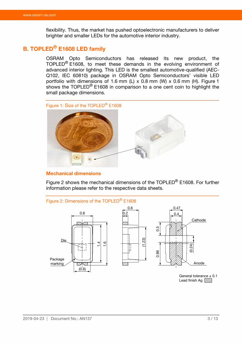
OSRAM Opto Semiconductors has released its new product, theTOPLED® E1608, to meet these demands in the evolving environment ofadvanced interior lighting. This LED is the smallest automotive-qualified (AEC-Q102, IEC 60810) package in OSRAM Opto Semiconductors’ visible LEDportfolio with dimensions of 1.6 mm (L) x 0.8 mm (W) x 0.6 mm (H). Figure 1shows the TOPLED® E1608 in comparison to a one cent coin to highlight thesmall package dimensions.
Figure 1: Size of the TOPLED® E1608
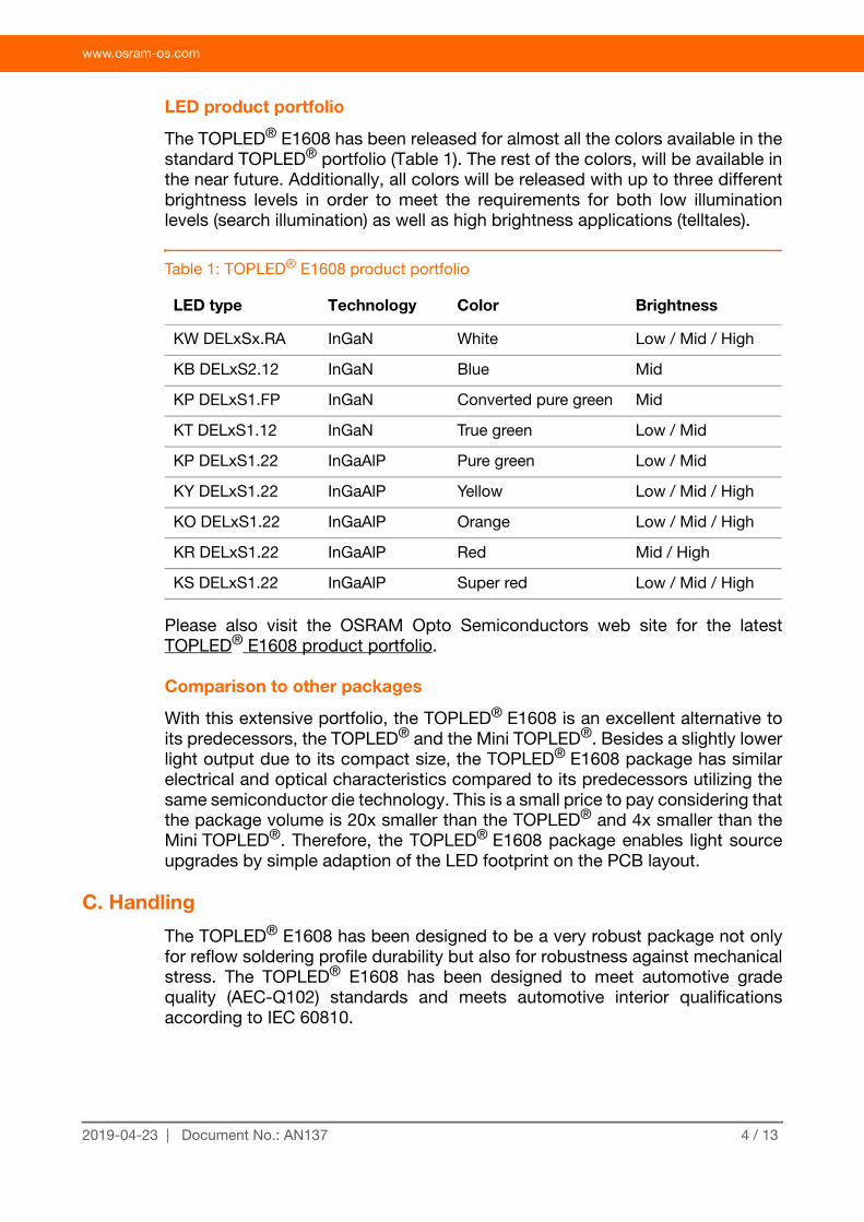
Mechanical dimensions
Figure 2 shows the mechanical dimensions of the TOPLED® E1608. For furtherinformation please refer to the respective data sheets.
Figure 2: Dimensions of the TOPLED® E1608
Cathode
Anode
0.47
0.4
0.5
0.86 (0
.24)(1
.23)
0.60.20.8
Die
Package marking
(0.6)
1.4
1.6
General tolerance ± 0.1Lead finish Ag
3 / 132019-04-23 | Document No.: AN137
www.osram-os.com
LED product portfolio
The TOPLED® E1608 has been released for almost all the colors available in thestandard TOPLED® portfolio (Table 1). The rest of the colors, will be available inthe near future. Additionally, all colors will be released with up to three differentbrightness levels in order to meet the requirements for both low illuminationlevels (search illumination) as well as high brightness applications (telltales).
Please also visit the OSRAM Opto Semiconductors web site for the latestTOPLED® E1608 product portfolio.
Comparison to other packages
With this extensive portfolio, the TOPLED® E1608 is an excellent alternative toits predecessors, the TOPLED® and the Mini TOPLED®. Besides a slightly lowerlight output due to its compact size, the TOPLED® E1608 package has similarelectrical and optical characteristics compared to its predecessors utilizing thesame semiconductor die technology. This is a small price to pay considering thatthe package volume is 20x smaller than the TOPLED® and 4x smaller than theMini TOPLED®. Therefore, the TOPLED® E1608 package enables light sourceupgrades by simple adaption of the LED footprint on the PCB layout.
C. Handling
The TOPLED® E1608 has been designed to be a very robust package not onlyfor reflow soldering profile durability but also for robustness against mechanicalstress. The TOPLED® E1608 has been designed to meet automotive gradequality (AEC-Q102) standards and meets automotive interior qualificationsaccording to IEC 60810.
Table 1: TOPLED® E1608 product portfolio
LED type Technology Color Brightness
KW DELxSx.RA InGaN White Low / Mid / High
KB DELxS2.12 InGaN Blue Mid
KP DELxS1.FP InGaN Converted pure green Mid
KT DELxS1.12 InGaN True green Low / Mid
KP DELxS1.22 InGaAlP Pure green Low / Mid
KY DELxS1.22 InGaAlP Yellow Low / Mid / High
KO DELxS1.22 InGaAlP Orange Low / Mid / High
KR DELxS1.22 InGaAlP Red Mid / High
KS DELxS1.22 InGaAlP Super red Low / Mid / High
4 / 132019-04-23 | Document No.: AN137
www.osram-os.com
ESD stability
The LED provides ESD stability of up to 2 kV. It is assigned to the “Class 2 HBM”category in accordance with ANSI / ESDA / JEDEC JS-001. With this class theTOPLED® E1608 can be considered as uncritical for processing and assemblyby state of the art SMT equipment aligned with ESD precautions. To achievehigher ESD protection on the system level, additional ESD protection should beapplied.
As is the case for all LEDs from OSRAM Opto Semiconductors, theTOPLED® E1608 also fulfills the current RoHS guidelines (European Union andChina) and therefore contains no lead or other defined hazardous substances.
Precaution and storage
Generally, the LEDs are packaged in tape and on reels. For storage anddispatch, the reels are packed in vacuum-sealed dry bags together withdesiccants. It is generally recommended to leave reels in their original packageuntil they are required, and to store components during processing underambient conditions of ≤ 10 % RH. Drying cabinets with dry nitrogen (N2) or dryair are suitable for this type of storage. The TOPLED® E1608 is declared tomoisture-sensitive Level 2 (MSL 2) according to JEDEC J-STD- 020E.
As with all LEDs from OSRAM Opto Semiconductors, the TOPLED® E1608 alsofulfills the current RoHS guidelines (European Union and China) and thereforecontains no lead or other defined hazardous substances.
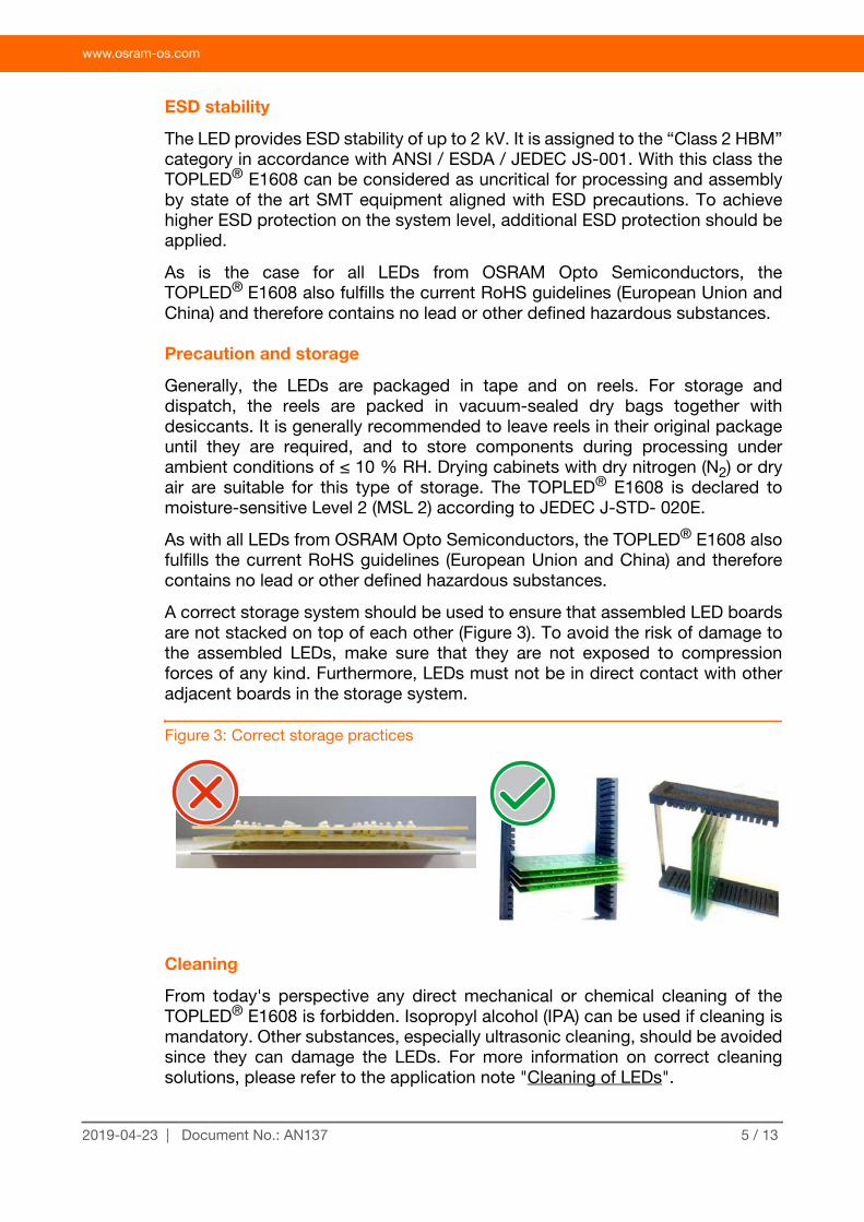
A correct storage system should be used to ensure that assembled LED boardsare not stacked on top of each other (Figure 3). To avoid the risk of damage tothe assembled LEDs, make sure that they are not exposed to compressionforces of any kind. Furthermore, LEDs must not be in direct contact with otheradjacent boards in the storage system.
Figure 3: Correct storage practices
Cleaning
From today's perspective any direct mechanical or chemical cleaning of theTOPLED® E1608 is forbidden. Isopropyl alcohol (IPA) can be used if cleaning ismandatory. Other substances, especially ultrasonic cleaning, should be avoidedsince they can damage the LEDs. For more information on correct cleaningsolutions, please refer to the application note "Cleaning of LEDs".
5 / 132019-04-23 | Document No.: AN137
www.osram-os.com
For dusty LEDs, simple cleaning by means of purified compressed air (e.g.central supply or spray can) with a air pressure of maximum 4 bar with a distanceof 20 cm to the component is recommended. Please consider that thecompressed air used is oil-free. Therefore the use of a spray can isrecommended.
In any case, all materials and methods should be tested beforehand, as towhether or not the component shows signs of damage.
Manual handling
Although manual handling and assembly is possible, automatic LED placementis recommended.
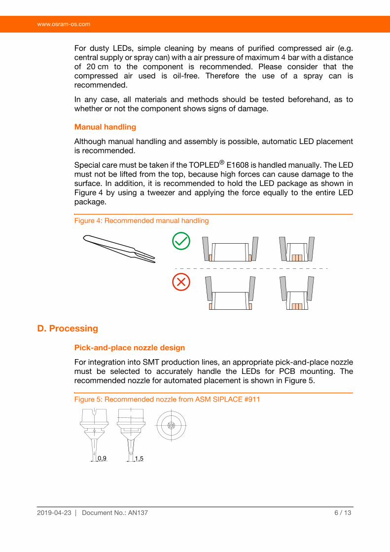
Special care must be taken if the TOPLED® E1608 is handled manually. The LEDmust not be lifted from the top, because high forces can cause damage to thesurface. In addition, it is recommended to hold the LED package as shown inFigure 4 by using a tweezer and applying the force equally to the entire LEDpackage.
Figure 4: Recommended manual handling
D. Processing
Pick-and-place nozzle design
For integration into SMT production lines, an appropriate pick-and-place nozzlemust be selected to accurately handle the LEDs for PCB mounting. Therecommended nozzle for automated placement is shown in Figure 5.
Figure 5: Recommended nozzle from ASM SIPLACE #911
0,9 1,5
6 / 132019-04-23 | Document No.: AN137
www.osram-os.com
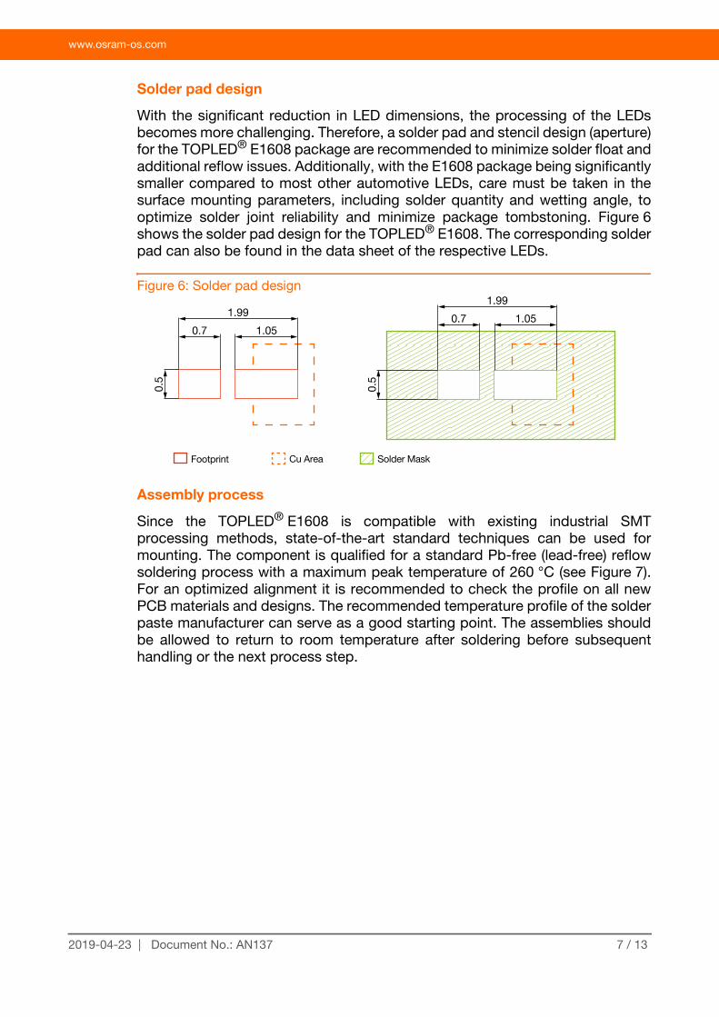
Solder pad design
With the significant reduction in LED dimensions, the processing of the LEDsbecomes more challenging. Therefore, a solder pad and stencil design (aperture)for the TOPLED® E1608 package are recommended to minimize solder float andadditional reflow issues. Additionally, with the E1608 package being significantlysmaller compared to most other automotive LEDs, care must be taken in thesurface mounting parameters, including solder quantity and wetting angle, tooptimize solder joint reliability and minimize package tombstoning. Figure 6shows the solder pad design for the TOPLED® E1608. The corresponding solderpad can also be found in the data sheet of the respective LEDs.
Figure 6: Solder pad design
Assembly process
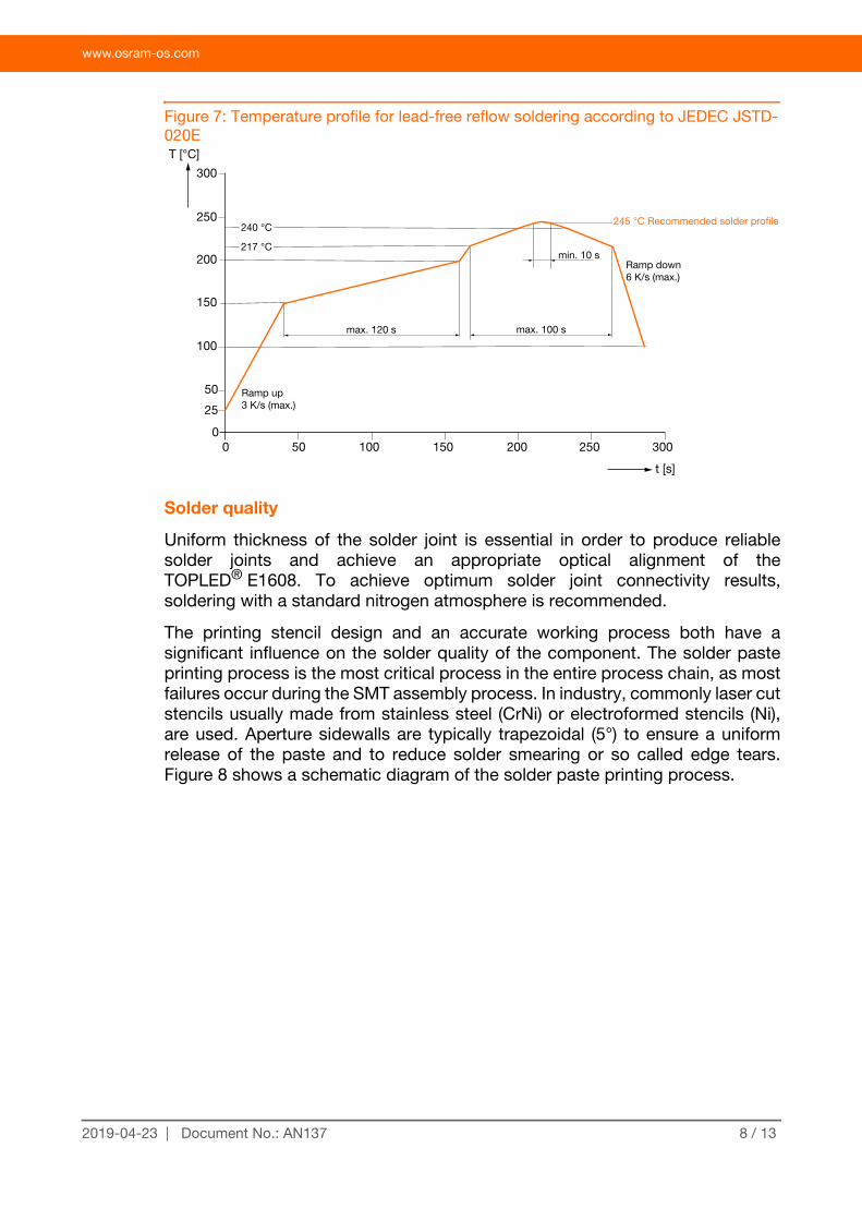
Since the TOPLED® E1608 is compatible with existing industrial SMTprocessing methods, state-of-the-art standard techniques can be used formounting. The component is qualified for a standard Pb-free (lead-free) reflowsoldering process with a maximum peak temperature of 260 °C (see Figure 7).For an optimized alignment it is recommended to check the profile on all newPCB materials and designs. The recommended temperature profile of the solderpaste manufacturer can serve as a good starting point. The assemblies shouldbe allowed to return to room temperature after soldering before subsequenthandling or the next process step.
Cu Area Solder MaskFootprint
0.7
0.5
1.05
1.99 0.7
0.5
1.05
1.99
7 / 132019-04-23 | Document No.: AN137
www.osram-os.com
Figure 7: Temperature profile for lead-free reflow soldering according to JEDEC JSTD-020E
Solder quality
Uniform thickness of the solder joint is essential in order to produce reliablesolder joints and achieve an appropriate optical alignment of theTOPLED® E1608. To achieve optimum solder joint connectivity results,soldering with a standard nitrogen atmosphere is recommended.
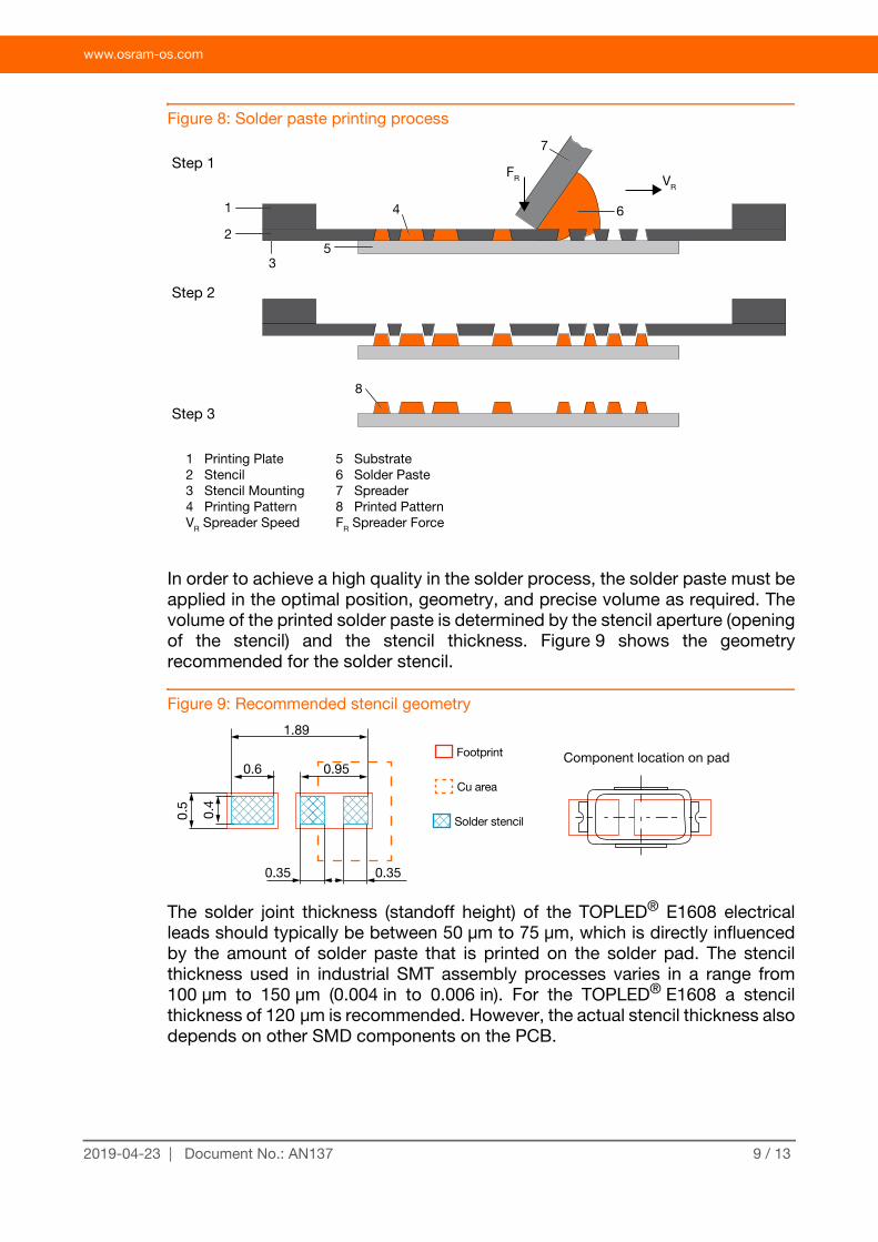
The printing stencil design and an accurate working process both have asignificant influence on the solder quality of the component. The solder pasteprinting process is the most critical process in the entire process chain, as mostfailures occur during the SMT assembly process. In industry, commonly laser cutstencils usually made from stainless steel (CrNi) or electroformed stencils (Ni),are used. Aperture sidewalls are typically trapezoidal (5°) to ensure a uniformrelease of the paste and to reduce solder smearing or so called edge tears.Figure 8 shows a schematic diagram of the solder paste printing process.
0 50 100 150 200 250 300
t [s]
0
50
100
150
200
250
300
25
T [°C]
max. 120 s
min. 10 s
max. 100 s
Ramp up3 K/s (max.)
Ramp down6 K/s (max.)
245 °C Recommended solder profile
217 °C
240 °C
8 / 132019-04-23 | Document No.: AN137
www.osram-os.com
Figure 8: Solder paste printing process
In order to achieve a high quality in the solder process, the solder paste must beapplied in the optimal position, geometry, and precise volume as required. Thevolume of the printed solder paste is determined by the stencil aperture (openingof the stencil) and the stencil thickness. Figure 9 shows the geometryrecommended for the solder stencil.
Figure 9: Recommended stencil geometry
The solder joint thickness (standoff height) of the TOPLED® E1608 electricalleads should typically be between 50 μm to 75 μm, which is directly influencedby the amount of solder paste that is printed on the solder pad. The stencilthickness used in industrial SMT assembly processes varies in a range from100 μm to 150 μm (0.004 in to 0.006 in). For the TOPLED® E1608 a stencilthickness of 120 μm is recommended. However, the actual stencil thickness alsodepends on other SMD components on the PCB.
Step 1
Step 2
Step 3
1
3
2
4
7
FR VR
6
5
8
1 Printing Plate2 Stencil3 Stencil Mounting4 Printing PatternVR Spreader Speed
5 Substrate6 Solder Paste7 Spreader8 Printed PatternFR Spreader Force
Cu area
Solder stencil
Footprint0.6
0.4
0.95
1.89
0.35 0.35
Component location on pad
0.5
9 / 132019-04-23 | Document No.: AN137
www.osram-os.com
E. Automotive applications
Thin profile designs, thin lightguides
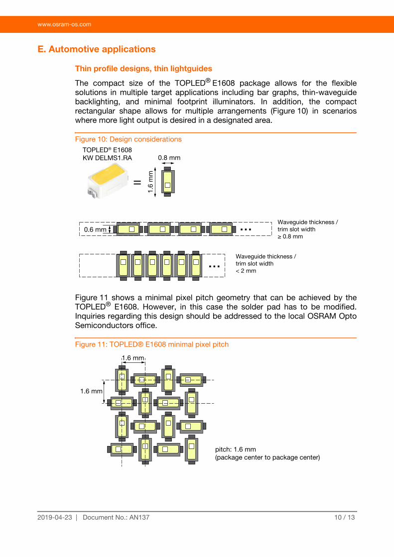
The compact size of the TOPLED® E1608 package allows for the flexiblesolutions in multiple target applications including bar graphs, thin-waveguidebacklighting, and minimal footprint illuminators. In addition, the compactrectangular shape allows for multiple arrangements (Figure 10) in scenarioswhere more light output is desired in a designated area.
Figure 10: Design considerations
Figure 11 shows a minimal pixel pitch geometry that can be achieved by theTOPLED® E1608. However, in this case the solder pad has to be modified.Inquiries regarding this design should be addressed to the local OSRAM OptoSemiconductors office.
Figure 11: TOPLED® E1608 minimal pixel pitch
1.6
mm
0.8 mm
=
0.6 mm …
…
TOPLED® E1608KW DELMS1.RA
Waveguide thickness /trim slot width≥ 0.8 mm
Waveguide thickness /trim slot width< 2 mm
1.6 mm
1.6 mm
pitch: 1.6 mm (package center to package center)
10 / 132019-04-23 | Document No.: AN137
www.osram-os.com
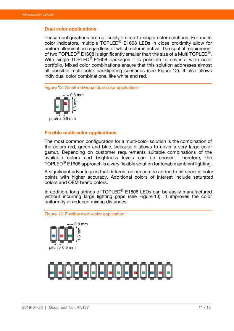
Dual color applications
These configurations are not solely limited to single color solutions. For multi-color indicators, multiple TOPLED® E1608 LEDs in close proximity allow foruniform illumination regardless of which color is active. The spatial requirementof two TOPLED® E1608 is significantly smaller than the size of a Multi TOPLED®.With single TOPLED® E1608 packages it is possible to cover a wide colorportfolio. Mixed color combinations ensure that this solution addresses almostall possible multi-color backlighting scenarios (see Figure 12). It also allowsindividual color combinations, like white and red.
Figure 12: Small individual dual color application
Flexible multi-color applications
The most common configuration for a multi-color solution is the combination of the colors red, green and blue, because it allows to cover a very large color gamut. Depending on customer requirements suitable combinations of the available colors and brightness levels can be chosen. Therefore, the TOPLED® E1608 approach is a very flexible solution for tunable ambient lighting.
A significant advantage is that different colors can be added to hit specific color points with higher accuracy. Additional colors of interest include saturated colors and OEM brand colors.
In addition, long strings of TOPLED® E1608 LEDs can be easily manufactured without incurring large lighting gaps (see Figure 13). It improves the color uniformity at reduced mixing distances.
Figure 13: Flexible multi-color application
1.6
mm
0.8 mm
pitch > 0.9 mm
1.6
mm
pitch > 0.9 mm
0.8 mm
11 / 132019-04-23 | Document No.: AN137
www.osram-os.com
F. Summary
The TOPLED® E1608 is primary designed for automotive interior applicationsand offers the smallest automotive-qualified package in the visible LED portfolioof OSRAM Opto Semiconductors. It is available in various colors and brightnesslevels in order to meet the requirements for almost all interior applications.
The compatibility to standard industrial SMT processing methods is given, sothat excising population techniques can be used for the mounting process. Dueto the small package size of the LED, special care must be taken at the surfacemounting parameters.
The compact size of the TOPLED® E1608 package allows a flexible solution forvarious automotive interior applications such as for thin profile designs, narrowwaveguides or multiple LED arrangements. In addition, dual and multi colorapplications can also be realized by the TOPLED® E1608, requiring small space.
12 / 132019-04-23 | Document No.: AN137
www.osram-os.com
Don't forget: LED Light for you is your place tobe whenever you are looking for information orworldwide partners for your LED Lightingproject.
www.ledlightforyou.com
ABOUT OSRAM OPTO SEMICONDUCTORS
OSRAM, Munich, Germany is one of the two leading light manufacturers in the world. Its subsidiary, OSRAMOpto Semiconductors GmbH in Regensburg (Germany), offers its customers solutions based on semiconduc-tor technology for lighting, sensor and visualization applications. OSRAM Opto Semiconductors has produc-tion sites in Regensburg (Germany), Penang (Malaysia) and Wuxi (China). Its headquarters for North Americais in Sunnyvale (USA), and for Asia in Hong Kong. OSRAM Opto Semiconductors also has sales offices th-roughout the world. For more information go to www.osram-os.com.
DISCLAIMER
PLEASE CAREFULLY READ THE BELOW TERMS AND CONDITIONS BEFORE USING THE INFORMA-TION SHOWN HEREIN. IF YOU DO NOT AGREE WITH ANY OF THESE TERMS AND CONDITIONS, DONOT USE THE INFORMATION.
The information provided in this general information document was formulated using the utmost care; howe-ver, it is provided by OSRAM Opto Semiconductors GmbH on an “as is” basis. Thus, OSRAM Opto Semicon-ductors GmbH does not expressly or implicitly assume any warranty or liability whatsoever in relation to thisinformation, including – but not limited to – warranties for correctness, completeness, marketability, fitnessfor any specific purpose, title, or non-infringement of rights. In no event shall OSRAM Opto SemiconductorsGmbH be liable – regardless of the legal theory – for any direct, indirect, special, incidental, exemplary, con-sequential, or punitive damages arising from the use of this information. This limitation shall apply even ifOSRAM Opto Semiconductors GmbH has been advised of possible damages. As some jurisdictions do notallow the exclusion of certain warranties or limitations of liabilities, the above limitations and exclusions mightnot apply. In such cases, the liability of OSRAM Opto Semiconductors GmbH is limited to the greatest extentpermitted in law.
OSRAM Opto Semiconductors GmbH may change the provided information at any time without giving noticeto users and is not obliged to provide any maintenance or support related to the provided information. Theprovided information is based on special conditions, which means that the possibility of changes cannot beprecluded.
Any rights not expressly granted herein are reserved. Other than the right to use the information provided inthis document, no other rights are granted nor shall any obligations requiring the granting of further rights beinferred. Any and all rights and licenses regarding patents and patent applications are expressly excluded.
It is prohibited to reproduce, transfer, distribute, or store all or part of the content of this document in any formwithout the prior written permission of OSRAM Opto Semiconductors GmbH unless required to do so in ac-cordance with applicable law.
OSRAM Opto Semiconductors GmbH
Head office:
Leibnizstr. 493055 RegensburgGermanywww.osram-os.com
13 / 132019-04-23 | Document No.: AN137