AN11024 SDARS active antenna 2nd stage LNA with … information AN11024 SDARS active antenna 2nd...
19
AN11024 SDARS active antenna 2nd stage LNA with BFU690, 2.33 GHz Rev. 1 — 24 March 2011 Application note Document information Info Content Keywords LNA, 2.33 GHz, BFU690, SDARS Abstract This application note provides circuit, layout, BOM and performance information for 2.33GHz LNA equipped with NXP Semiconductors BFU690 wideband transistor
Transcript of AN11024 SDARS active antenna 2nd stage LNA with … information AN11024 SDARS active antenna 2nd...
AN11024SDARS active antenna 2nd stage LNA with BFU690, 2.33 GHzRev. 1 — 24 March 2011 Application note
Document information
Info Content
Keywords LNA, 2.33 GHz, BFU690, SDARS
Abstract This application note provides circuit, layout, BOM and performance information for 2.33GHz LNA equipped with NXP Semiconductors BFU690 wideband transistor

NXP Semiconductors AN11024SDARS active antenna 2nd stage LNA with BFU690, 2.33 GHz
Revision history
Rev Date Description
v.1 20110324 initial version
AN11024 All information provided in this document is subject to legal disclaimers. © NXP B.V. 2011. All rights reserved.
Application note Rev. 1 — 24 March 2011 2 of 19
Contact informationFor more information, please visit: http://www.nxp.com
For sales office addresses, please send an email to: [email protected]
NXP Semiconductors AN11024SDARS active antenna 2nd stage LNA with BFU690, 2.33 GHz
1. Introduction
The BFU690 is a wideband Silicon Germanium Amplifier transistor intended for high speed, low noise applications. It is designed to be used for LNA applications such as GPS, satellite radio, cordless phone and wireless LAN. The BFU690 comes in a SOT343F package providing 2 emitter pins for better grounding.
The BFU690 is ideal in all kind of applications where cost matters. It also gives the designer flexibility in his design work.
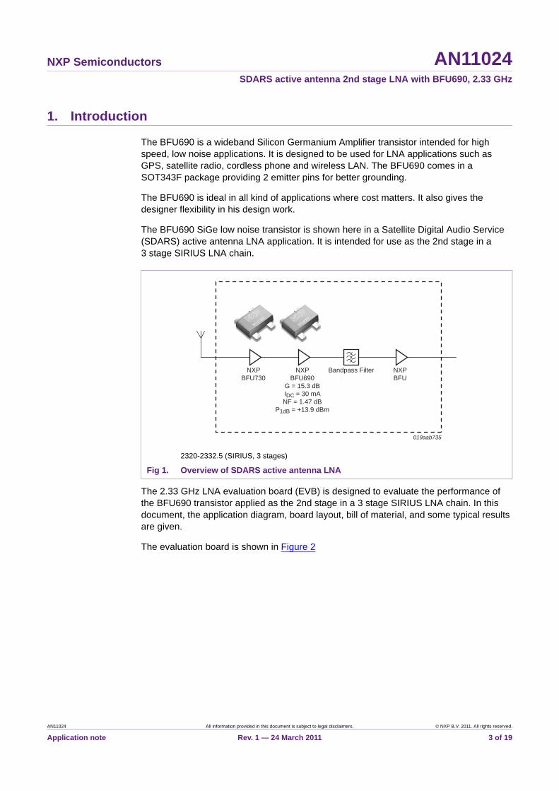
The BFU690 SiGe low noise transistor is shown here in a Satellite Digital Audio Service (SDARS) active antenna LNA application. It is intended for use as the 2nd stage in a 3 stage SIRIUS LNA chain.
The 2.33 GHz LNA evaluation board (EVB) is designed to evaluate the performance of the BFU690 transistor applied as the 2nd stage in a 3 stage SIRIUS LNA chain. In this document, the application diagram, board layout, bill of material, and some typical results are given.
The evaluation board is shown in Figure 2
2320-2332.5 (SIRIUS, 3 stages)
Fig 1. Overview of SDARS active antenna LNA
019aab735
NXPBFU730
NXPBFU
Bandpass FilterNXPBFU690
G = 15.3 dBIDC = 30 mANF = 1.47 dB
P1dB = +13.9 dBm
AN11024 All information provided in this document is subject to legal disclaimers. © NXP B.V. 2011. All rights reserved.
Application note Rev. 1 — 24 March 2011 3 of 19

NXP Semiconductors AN11024SDARS active antenna 2nd stage LNA with BFU690, 2.33 GHz
2. General description
The BFU690 is a NPN silicon germanium microwave transistor for high speed, low noise applications in a plastic, 4-pin dual-emitter SOT343F package. Table 1 shows a summary of the transistor performance in terms of noise and gain.
Fig 2. BFU690, 2.33 GHz LNA evaluation board
019aab736
Table 1. BFU690 performance in terms of noise and gain measured at VCE = 2 V; IC = 25 mA
Frequency (GHz) Noise figure (dB) Associated gain (dB)
1.5 1.13 19.5
2.4 1.51 15.7
Table 2. BFU690 pinning information
Pin Description Simplified outline Graphic symbol
1 emitter
2 base
3 emitter
4 collector
12
3 4
mbb159
4
1, 3
2
AN11024 All information provided in this document is subject to legal disclaimers. © NXP B.V. 2011. All rights reserved.
Application note Rev. 1 — 24 March 2011 4 of 19
NXP Semiconductors AN11024SDARS active antenna 2nd stage LNA with BFU690, 2.33 GHz
3. Application board
The BFU690 2.33GHz EVB simplifies the evaluation of the BFU690 wideband transistor, for this frequency range. The EVB enables testing of the device performance and requires no additional support circuitry. The board is fully assembled with the BFU690, including input and output matching, to optimize the performance. The input match was a compromise between the best noise figure and a low input return loss. The board is mounted with signal input and output SMA connectors for connection to RF test equipment:
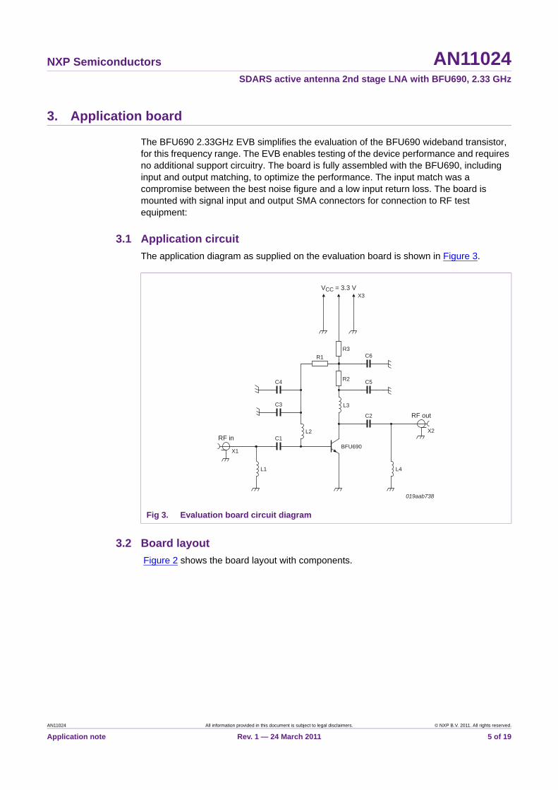
3.1 Application circuit
The application diagram as supplied on the evaluation board is shown in Figure 3.
3.2 Board layout
Figure 2 shows the board layout with components.
Fig 3. Evaluation board circuit diagram
C4
L2
L3
R2
R3C6
C5
C2
L4
X3
C3
C1
L1
X1
X2
BFU690
R1
VCC = 3.3 V
RF in
RF out
019aab738
AN11024 All information provided in this document is subject to legal disclaimers. © NXP B.V. 2011. All rights reserved.
Application note Rev. 1 — 24 March 2011 5 of 19

NXP Semiconductors AN11024SDARS active antenna 2nd stage LNA with BFU690, 2.33 GHz
3.3 PCB layout
A good PCB Layout is an essential part of an RF circuit design. The EVB of the BFU690 can serve as a guideline for laying out a board using either the BFU690. Use controlled impedance lines for all high frequency inputs and outputs. Bypass supply voltage VCC with decoupling capacitors, preferable located as close as possible to the device. For long bias lines it may be necessary to add decoupling capacitors along the line further away from the device. Proper grounding of the GND pin is also essential for the performance. Either connect the GND pin directly to the ground plane or through vias, or do both.
The EVB is made of FR4 material using the stack shown in Figure 5
Fig 4. Component layout for the BUF690 2.33 GHz evaluation board
019aab739
Material supplier Isola Duraver;r = 4.6 to 4.9; T = 0.02
Fig 5. Stack of PCB material
019aab740
17 µm Cu
17 µm Cu
17 µm Cu
17 µm Cu
0.25 mm FR4 Critical
0.50 mm FR4 only formechanical rigidity of PCB
0.25 mm FR4 only formechanical rigidity of PCB
AN11024 All information provided in this document is subject to legal disclaimers. © NXP B.V. 2011. All rights reserved.
Application note Rev. 1 — 24 March 2011 6 of 19
NXP Semiconductors AN11024SDARS active antenna 2nd stage LNA with BFU690, 2.33 GHz
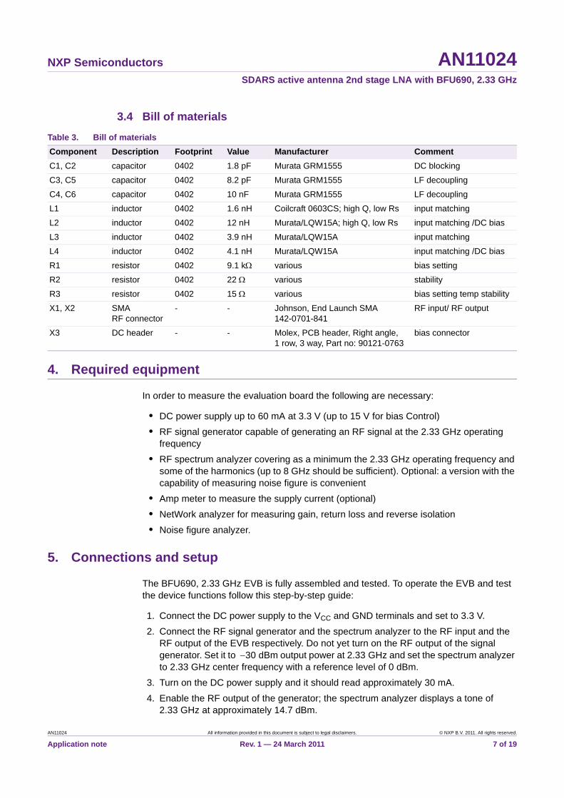
3.4 Bill of materials
4. Required equipment
In order to measure the evaluation board the following are necessary:
• DC power supply up to 60 mA at 3.3 V (up to 15 V for bias Control)
• RF signal generator capable of generating an RF signal at the 2.33 GHz operating frequency
• RF spectrum analyzer covering as a minimum the 2.33 GHz operating frequency and some of the harmonics (up to 8 GHz should be sufficient). Optional: a version with the capability of measuring noise figure is convenient
• Amp meter to measure the supply current (optional)
• NetWork analyzer for measuring gain, return loss and reverse isolation
• Noise figure analyzer.
5. Connections and setup
The BFU690, 2.33 GHz EVB is fully assembled and tested. To operate the EVB and test the device functions follow this step-by-step guide:
1. Connect the DC power supply to the VCC and GND terminals and set to 3.3 V.
2. Connect the RF signal generator and the spectrum analyzer to the RF input and the RF output of the EVB respectively. Do not yet turn on the RF output of the signal generator. Set it to 30 dBm output power at 2.33 GHz and set the spectrum analyzer to 2.33 GHz center frequency with a reference level of 0 dBm.
3. Turn on the DC power supply and it should read approximately 30 mA.
4. Enable the RF output of the generator; the spectrum analyzer displays a tone of 2.33 GHz at approximately 14.7 dBm.
Table 3. Bill of materials
Component Description Footprint Value Manufacturer Comment
C1, C2 capacitor 0402 1.8 pF Murata GRM1555 DC blocking
C3, C5 capacitor 0402 8.2 pF Murata GRM1555 LF decoupling
C4, C6 capacitor 0402 10 nF Murata GRM1555 LF decoupling
L1 inductor 0402 1.6 nH Coilcraft 0603CS; high Q, low Rs input matching
L2 inductor 0402 12 nH Murata/LQW15A; high Q, low Rs input matching /DC bias
L3 inductor 0402 3.9 nH Murata/LQW15A input matching
L4 inductor 0402 4.1 nH Murata/LQW15A input matching /DC bias
R1 resistor 0402 9.1 k various bias setting
R2 resistor 0402 22 various stability
R3 resistor 0402 15 various bias setting temp stability
X1, X2 SMA RF connector
- - Johnson, End Launch SMA 142-0701-841
RF input/ RF output
X3 DC header - - Molex, PCB header, Right angle, 1 row, 3 way, Part no: 90121-0763
bias connector
AN11024 All information provided in this document is subject to legal disclaimers. © NXP B.V. 2011. All rights reserved.
Application note Rev. 1 — 24 March 2011 7 of 19

NXP Semiconductors AN11024SDARS active antenna 2nd stage LNA with BFU690, 2.33 GHz
5. A NetWork Analyzer (NWA) can be used instead of a signal generator and spectrum analyzer in order to measure both gain and input and output return losses.
6. For noise figure evaluation use either a noise figure analyzer or a spectrum analyzer with noise option. The use of a 15 dB noise source, such as the Agilent 364B is recommended. When measuring the noise figure of the evaluation board, any kind of adaptors, cables etc, between the noise source and the EVB should be avoided, since this affects the noise performance.
6. Typical EVB results
Fig 6. Evaluation board showing its connections
019aab741
RFin RFout
VCC GND
Table 4. Typical results measured on the evaluation boardT = 25 C; f = 2.33 GHz unless otherwise specified
Symbol Parameter BFU690 EVB Unit
NF noise figure 1.47[1] dB
Gp power gain 15.3[1] dB
IRL input return loss 10 dB
ORL output return loss 17 dB
isol(r) reverse isolation 20.7 dB
Pi(1dB) input power at 1 dB gain compression
0.48 dBm
AN11024 All information provided in this document is subject to legal disclaimers. © NXP B.V. 2011. All rights reserved.
Application note Rev. 1 — 24 March 2011 8 of 19

NXP Semiconductors AN11024SDARS active antenna 2nd stage LNA with BFU690, 2.33 GHz
[1] The NF and gain figures are measured at the SMA connectors of the EVB, so the connector and PCB losses are not subtracted. If subtracted the NF will improve by approximately 0.1 dB.
6.1 Noise figure
PL(1dB) output power at 1 dB gain compression
13.9 dBm
IP3i input third order intercept point
12.85 dBm
IP3o output third order intercept point
28.15 dBm
Table 4. Typical results measured on the evaluation board …continuedT = 25 C; f = 2.33 GHz unless otherwise specified
Symbol Parameter BFU690 EVB Unit
2290 MHz to 2390 MHz.
Center of plot (x-axis) is 2333 MHz.
Ref = 62 dBm, SWT = 100 ms.
(1) Gain.
(2) NF.
Fig 7. Noise figure plot
Table 5. Noise figure tabular dataFrom Rohde & Schwarz FSU
Frequency list results
RF (GHz) NF (dB) Noise temp (K) Gain (dB)
2.290 1.456 115.508 15.758
2.300 1.445 114.499 15.699
2.310 1.445 114.486 15.601
2.320 1.450 114.944 15.468
2.330 1.468 116.673 15.297
2.340 1.499 119.495 15.124
(RF)2.290 Ghz 2.390 GHz10.000 MHz/div
019aab742
2
3
1
4
5
0
10
12
8
14
16
6
(2)
(1)NF G
AN11024 All information provided in this document is subject to legal disclaimers. © NXP B.V. 2011. All rights reserved.
Application note Rev. 1 — 24 March 2011 9 of 19

NXP Semiconductors AN11024SDARS active antenna 2nd stage LNA with BFU690, 2.33 GHz
6.2 Gain compression test
The network analyzer is set to CW mode: e.g. set to a single frequency, with power sweep. Input power is swept from 25 dBm to +5 dBm at 2332.5 MHz. The amplifier reaches input 1 dB compression point (Pi(1dB)) at 0.48 dBm input power.Output PL(1dB) = 0.48 dBm + 14.4 dB gain at PL(1dB) point +13.9 dBm, or 24.5 mW
2.350 1.528 122.291 14.968
2.360 1.564 125.712 14.875
2.370 1.587 127.888 14.822
2.380 1.601 129.290 14.810
2.390 1.607 129.874 14.750
Table 5. Noise figure tabular data …continuedFrom Rohde & Schwarz FSU
Frequency list results
RF (GHz) NF (dB) Noise temp (K) Gain (dB)
(1) Tr 3 b2/a1.1 LogM 10.00 dBm/0.00 dBm: 25.0000 dBm; 15.396 dB.
(2) Tr 3 b2/a1.1 LogM 10.00 dBm/ 0.00 dBm: 480.0000 mdBm; 14.432 dB.
(3) Tr 2 b2/1 LogM 10.00 dBm/ 0.00 dBm: 480.0000 mdBm; 13.902 dBm.
Fig 8. Gain compression test plot
>Ch1: Start -25.000 dBm
Stop 5.000 dBm
CW 2.33250
019aab744
-10.00
10.00
-30.00
30.00
50.00
-50.00
(3)
(2)(1)
AN11024 All information provided in this document is subject to legal disclaimers. © NXP B.V. 2011. All rights reserved.
Application note Rev. 1 — 24 March 2011 10 of 19

NXP Semiconductors AN11024SDARS active antenna 2nd stage LNA with BFU690, 2.33 GHz
6.3 Input return losses
6.3.1 Log Mag
10 MHz to 6 GHz.
Tr 1 S11 LogM 2.000 dB/10.0 dB.
(1) 2.320000 GHz; 10.632 dB.
(2) 2.345000 GHz; 9.0084 dB.
Fig 9. Input return loss plot
>Ch1: Start 10.000 MHz Stop 6.00000 Ghz
019aab745
-12.00
-8.00
-16.00
-4.00
0.00
-20.00
(1)
(2)
AN11024 All information provided in this document is subject to legal disclaimers. © NXP B.V. 2011. All rights reserved.
Application note Rev. 1 — 24 March 2011 11 of 19
NXP Semiconductors AN11024SDARS active antenna 2nd stage LNA with BFU690, 2.33 GHz
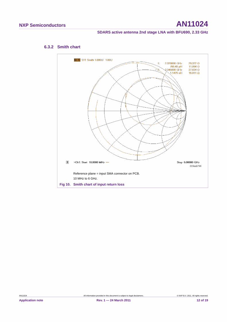
6.3.2 Smith chart
Reference plane = input SMA connector on PCB.
10 MHz to 6 GHz.
Fig 10. Smith chart of input return loss
019aab746
AN11024 All information provided in this document is subject to legal disclaimers. © NXP B.V. 2011. All rights reserved.
Application note Rev. 1 — 24 March 2011 12 of 19
NXP Semiconductors AN11024SDARS active antenna 2nd stage LNA with BFU690, 2.33 GHz
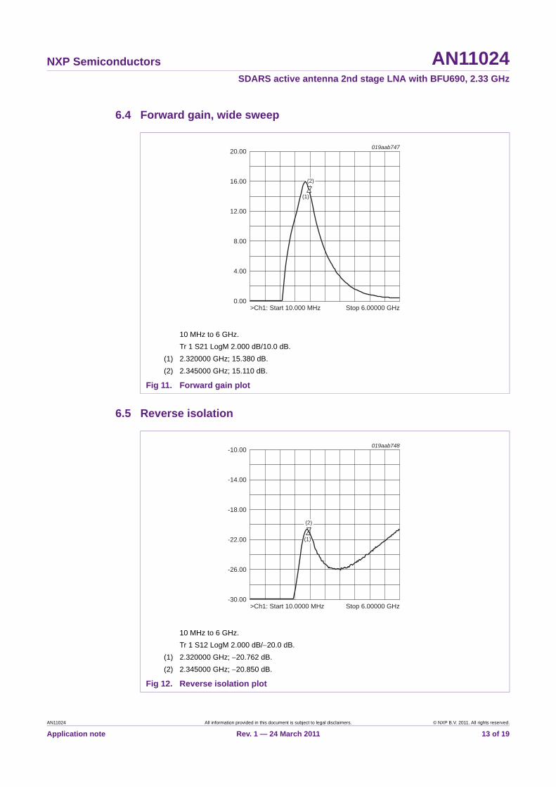
6.4 Forward gain, wide sweep
6.5 Reverse isolation
10 MHz to 6 GHz.
Tr 1 S21 LogM 2.000 dB/10.0 dB.
(1) 2.320000 GHz; 15.380 dB.
(2) 2.345000 GHz; 15.110 dB.
Fig 11. Forward gain plot
>Ch1: Start 10.000 MHz Stop 6.00000 GHz
019aab747
8.00
12.00
4.00
16.00
20.00
0.00
(2)
(1)
10 MHz to 6 GHz.
Tr 1 S12 LogM 2.000 dB/20.0 dB.
(1) 2.320000 GHz; 20.762 dB.
(2) 2.345000 GHz; 20.850 dB.
Fig 12. Reverse isolation plot
>Ch1: Start 10.0000 MHz Stop 6.00000 GHz
019aab748
-22.00
-18.00
-26.00
-14.00
-10.00
-30.00
(2)
(1)
AN11024 All information provided in this document is subject to legal disclaimers. © NXP B.V. 2011. All rights reserved.
Application note Rev. 1 — 24 March 2011 13 of 19

NXP Semiconductors AN11024SDARS active antenna 2nd stage LNA with BFU690, 2.33 GHz
6.6 Output return losses
6.6.1 Log Mag
10 MHz to 6 GHz.
Tr 1 S22 LogM 2.000 dB/10.0 dB.
(1) 2.320000 GHz; 19.453 dB.
(2) 2.345000 GHz; 16.948 dB.
Fig 13. Output return loss plot
(1)
>Ch1: Start 10.0000 MHz Stop 6.00000 GHz
019aab749
-12.00
-8.00
-16.00
-4.00
0.00
-20.00
(2)
AN11024 All information provided in this document is subject to legal disclaimers. © NXP B.V. 2011. All rights reserved.
Application note Rev. 1 — 24 March 2011 14 of 19

NXP Semiconductors AN11024SDARS active antenna 2nd stage LNA with BFU690, 2.33 GHz
6.6.2 Smith chart
Reference plane = input SMA connector on PCB.
10 MHz to 6 GHz.
Fig 14. Smith chart of output return loss
019aab750
AN11024 All information provided in this document is subject to legal disclaimers. © NXP B.V. 2011. All rights reserved.
Application note Rev. 1 — 24 March 2011 15 of 19
NXP Semiconductors AN11024SDARS active antenna 2nd stage LNA with BFU690, 2.33 GHz
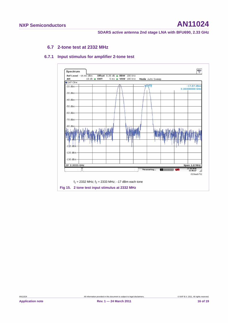
6.7 2-tone test at 2332 MHz
6.7.1 Input stimulus for amplifier 2-tone test
f1 = 2332 MHz; f2 = 2333 MHz; 17 dBm each tone
Fig 15. 2 tone test input stimulus at 2332 MHz
019aab751
AN11024 All information provided in this document is subject to legal disclaimers. © NXP B.V. 2011. All rights reserved.
Application note Rev. 1 — 24 March 2011 16 of 19
NXP Semiconductors AN11024SDARS active antenna 2nd stage LNA with BFU690, 2.33 GHz
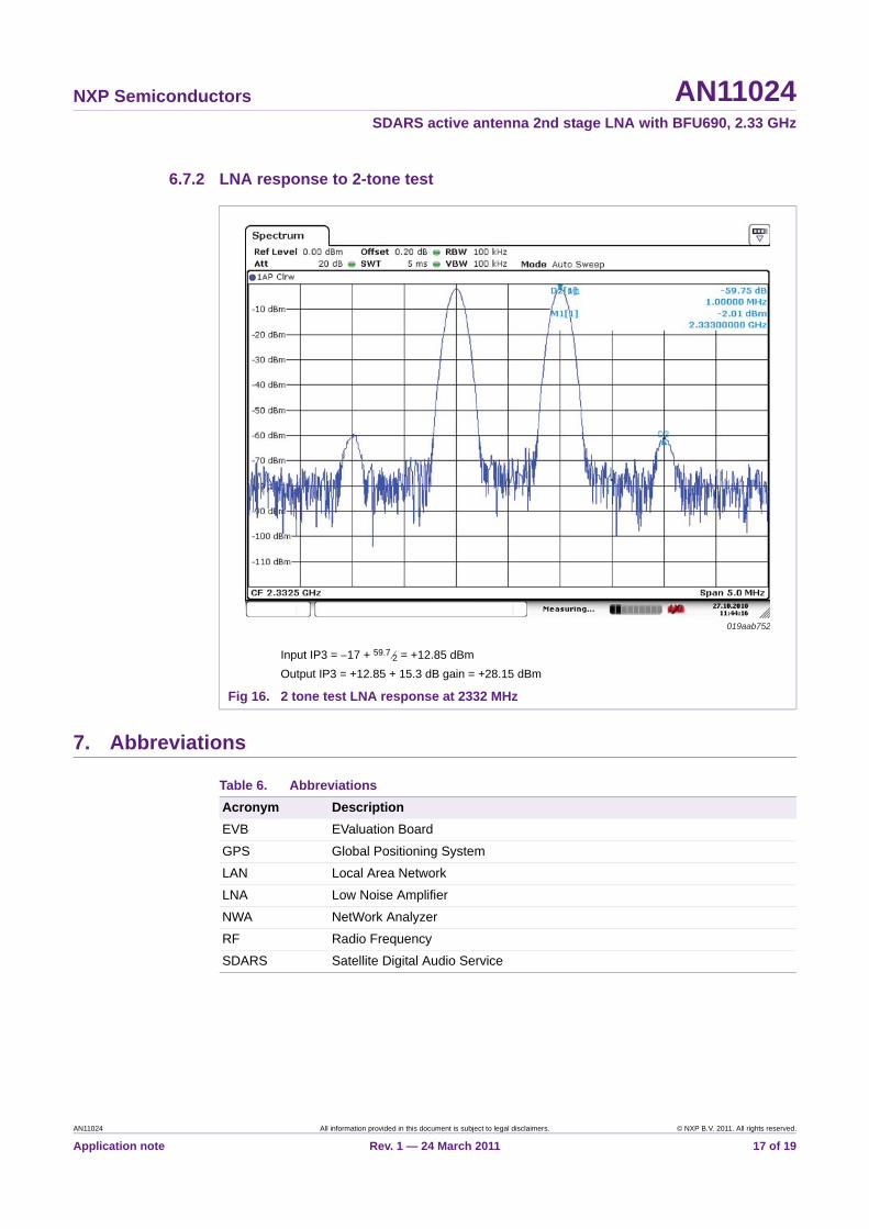
6.7.2 LNA response to 2-tone test
7. Abbreviations
Input IP3 = 17 + 59.72 = +12.85 dBm
Output IP3 = +12.85 + 15.3 dB gain = +28.15 dBm
Fig 16. 2 tone test LNA response at 2332 MHz
019aab752
Table 6. Abbreviations
Acronym Description
EVB EValuation Board
GPS Global Positioning System
LAN Local Area Network
LNA Low Noise Amplifier
NWA NetWork Analyzer
RF Radio Frequency
SDARS Satellite Digital Audio Service
AN11024 All information provided in this document is subject to legal disclaimers. © NXP B.V. 2011. All rights reserved.
Application note Rev. 1 — 24 March 2011 17 of 19
NXP Semiconductors AN11024SDARS active antenna 2nd stage LNA with BFU690, 2.33 GHz
8. Legal information
8.1 Definitions
Draft — The document is a draft version only. The content is still under internal review and subject to formal approval, which may result in modifications or additions. NXP Semiconductors does not give any representations or warranties as to the accuracy or completeness of information included herein and shall have no liability for the consequences of use of such information.
8.2 Disclaimers
Limited warranty and liability — Information in this document is believed to be accurate and reliable. However, NXP Semiconductors does not give any representations or warranties, expressed or implied, as to the accuracy or completeness of such information and shall have no liability for the consequences of use of such information.
In no event shall NXP Semiconductors be liable for any indirect, incidental, punitive, special or consequential damages (including - without limitation - lost profits, lost savings, business interruption, costs related to the removal or replacement of any products or rework charges) whether or not such damages are based on tort (including negligence), warranty, breach of contract or any other legal theory.
Notwithstanding any damages that customer might incur for any reason whatsoever, NXP Semiconductors’ aggregate and cumulative liability towards customer for the products described herein shall be limited in accordance with the Terms and conditions of commercial sale of NXP Semiconductors.
Right to make changes — NXP Semiconductors reserves the right to make changes to information published in this document, including without limitation specifications and product descriptions, at any time and without notice. This document supersedes and replaces all information supplied prior to the publication hereof.
Suitability for use — NXP Semiconductors products are not designed, authorized or warranted to be suitable for use in life support, life-critical or safety-critical systems or equipment, nor in applications where failure or malfunction of an NXP Semiconductors product can reasonably be expected to result in personal injury, death or severe property or environmental damage. NXP Semiconductors accepts no liability for inclusion and/or use of NXP Semiconductors products in such equipment or applications and therefore such inclusion and/or use is at the customer’s own risk.
Applications — Applications that are described herein for any of these products are for illustrative purposes only. NXP Semiconductors makes no representation or warranty that such applications will be suitable for the specified use without further testing or modification.
Customers are responsible for the design and operation of their applications and products using NXP Semiconductors products, and NXP Semiconductors accepts no liability for any assistance with applications or customer product
design. It is customer’s sole responsibility to determine whether the NXP Semiconductors product is suitable and fit for the customer’s applications and products planned, as well as for the planned application and use of customer’s third party customer(s). Customers should provide appropriate design and operating safeguards to minimize the risks associated with their applications and products.
NXP Semiconductors does not accept any liability related to any default, damage, costs or problem which is based on any weakness or default in the customer’s applications or products, or the application or use by customer’s third party customer(s). Customer is responsible for doing all necessary testing for the customer’s applications and products using NXP Semiconductors products in order to avoid a default of the applications and the products or of the application or use by customer’s third party customer(s). NXP does not accept any liability in this respect.
Export control — This document as well as the item(s) described herein may be subject to export control regulations. Export might require a prior authorization from national authorities.
Evaluation products — This product is provided on an “as is” and “with all faults” basis for evaluation purposes only. NXP Semiconductors, its affiliates and their suppliers expressly disclaim all warranties, whether express, implied or statutory, including but not limited to the implied warranties of non-infringement, merchantability and fitness for a particular purpose. The entire risk as to the quality, or arising out of the use or performance, of this product remains with customer.
In no event shall NXP Semiconductors, its affiliates or their suppliers be liable to customer for any special, indirect, consequential, punitive or incidental damages (including without limitation damages for loss of business, business interruption, loss of use, loss of data or information, and the like) arising out the use of or inability to use the product, whether or not based on tort (including negligence), strict liability, breach of contract, breach of warranty or any other theory, even if advised of the possibility of such damages.
Notwithstanding any damages that customer might incur for any reason whatsoever (including without limitation, all damages referenced above and all direct or general damages), the entire liability of NXP Semiconductors, its affiliates and their suppliers and customer’s exclusive remedy for all of the foregoing shall be limited to actual damages incurred by customer based on reasonable reliance up to the greater of the amount actually paid by customer for the product or five dollars (US$5.00). The foregoing limitations, exclusions and disclaimers shall apply to the maximum extent permitted by applicable law, even if any remedy fails of its essential purpose.
8.3 TrademarksNotice: All referenced brands, product names, service names and trademarks are the property of their respective owners.
AN11024 All information provided in this document is subject to legal disclaimers. © NXP B.V. 2011. All rights reserved.
Application note Rev. 1 — 24 March 2011 18 of 19

NXP Semiconductors AN11024SDARS active antenna 2nd stage LNA with BFU690, 2.33 GHz
9. Contents
1 Introduction . . . . . . . . . . . . . . . . . . . . . . . . . . . . 3
2 General description . . . . . . . . . . . . . . . . . . . . . . 4
3 Application board . . . . . . . . . . . . . . . . . . . . . . . 53.1 Application circuit . . . . . . . . . . . . . . . . . . . . . . . 53.2 Board layout . . . . . . . . . . . . . . . . . . . . . . . . . . . 53.3 PCB layout . . . . . . . . . . . . . . . . . . . . . . . . . . . . 63.4 Bill of materials . . . . . . . . . . . . . . . . . . . . . . . . . 7
4 Required equipment . . . . . . . . . . . . . . . . . . . . . 7
5 Connections and setup . . . . . . . . . . . . . . . . . . . 7
6 Typical EVB results . . . . . . . . . . . . . . . . . . . . . . 86.1 Noise figure . . . . . . . . . . . . . . . . . . . . . . . . . . . 96.2 Gain compression test . . . . . . . . . . . . . . . . . . 106.3 Input return losses . . . . . . . . . . . . . . . . . . . . . 116.3.1 Log Mag . . . . . . . . . . . . . . . . . . . . . . . . . . . . . 116.3.2 Smith chart . . . . . . . . . . . . . . . . . . . . . . . . . . . 126.4 Forward gain, wide sweep . . . . . . . . . . . . . . . 136.5 Reverse isolation . . . . . . . . . . . . . . . . . . . . . . 136.6 Output return losses . . . . . . . . . . . . . . . . . . . . 146.6.1 Log Mag . . . . . . . . . . . . . . . . . . . . . . . . . . . . . 146.6.2 Smith chart . . . . . . . . . . . . . . . . . . . . . . . . . . . 156.7 2-tone test at 2332 MHz . . . . . . . . . . . . . . . . . 166.7.1 Input stimulus for amplifier 2-tone test . . . . . . 166.7.2 LNA response to 2-tone test . . . . . . . . . . . . . . 17
7 Abbreviations. . . . . . . . . . . . . . . . . . . . . . . . . . 17
8 Legal information. . . . . . . . . . . . . . . . . . . . . . . 188.1 Definitions. . . . . . . . . . . . . . . . . . . . . . . . . . . . 188.2 Disclaimers . . . . . . . . . . . . . . . . . . . . . . . . . . . 188.3 Trademarks. . . . . . . . . . . . . . . . . . . . . . . . . . . 18
9 Contents . . . . . . . . . . . . . . . . . . . . . . . . . . . . . . 19
© NXP B.V. 2011. All rights reserved.
For more information, please visit: http://www.nxp.comFor sales office addresses, please send an email to: [email protected]
Date of release: 24 March 2011
Document identifier: AN11024
Please be aware that important notices concerning this document and the product(s)described herein, have been included in section ‘Legal information’.