An RF Amplifier for a FM - Radio Receiver 88-108 MHz · 2 Abstract An input amplifier for a...
18
An RF Amplifier for a FM - Radio Receiver 88-108 MHz Hongwu Tong E98 Fredrik Sverin E99 Radio Project 2003 Electroscience, Lund University
Transcript of An RF Amplifier for a FM - Radio Receiver 88-108 MHz · 2 Abstract An input amplifier for a...

An RF Amplifier for a FM - Radio Receiver
88-108 MHz
Hongwu Tong E98 Fredrik Sverin E99
Radio Project 2003 Electroscience, Lund University

2
Abstract An input amplifier for a FM-radio receiver with RF selection (88-108 MHz) has been designed in the radio project. It has about 25 dB gain in the frequency rang 88-108 MHz. Mirror frequency rejection is between 5 dB to 9 dB. Noise figure is about 7 dB at resonant frequency. The amplifier works well, when it is connected to the rest of circuits to receive FM broadcast signals.

3
Contents 1 INTRODUCTION........................................................................................... 4 2 PROJECT DESIGN........................................................................................ 5
2.1 TRANSISTOR SELECTION........................................................................... 5 2.2 S-PARAMETERS MEASUREMENT............................................................... 7 2.3 PROPERTY OF THE TRANSISTOR ................................................................ 8 2.4 TRANSISTOR BIASING ............................................................................. 10 2.5 FREQUENCY SELECTION ......................................................................... 11 2.6 COMPLETE DESIGN CIRCUIT ................................................................... 12
3 MEASUREMENT AND RESULT .............................................................. 13 3.1 GAIN....................................................................................................... 13 3.2 COMPRESSION POINT .............................................................................. 14 3.3 THIRD ORDER INTERCEPT POINT ............................................................ 15 3.4 NOISE FIGURE......................................................................................... 17
4 CONCLUSION.............................................................................................. 18 5 ACKNOWLEDGEMENT ............................................................................ 18 6 REFERENCES .............................................................................................. 18

4
1 Introduction The input amplifier with RF selection (88-108 MHz) should have low noise, high gain and frequency selection. The specification of the amplifier is as follows: 1 low noise, maximum 2dB more than Fmin 2 gain: Gt ≥ |S21|2 3 mirror frequency rejection: 20 dB 4 generator impedance: 50Ω 5 load impedance: 50Ω In order to fulfill the specification, an appropriate transistor was first chosen and its S-parameters were measured. The input stage has been designed by using a common-emitter amplifier. To compromise between gain and noise, an appropriate operating point is necessary. The amplifier has an inductor tap parallel resonant circuit at its collector to restore the amplifier gain. The frequency of the parallel resonant circuit can be shifted by changing the value of the parallel capacitor. The detail of the project design will be described in chapter 2. Different measurements and results can be found in chapter 3, followed by the conclusion in chapter 4. Chapter 5 is acknowledgement and reference is in chapter 6.
5
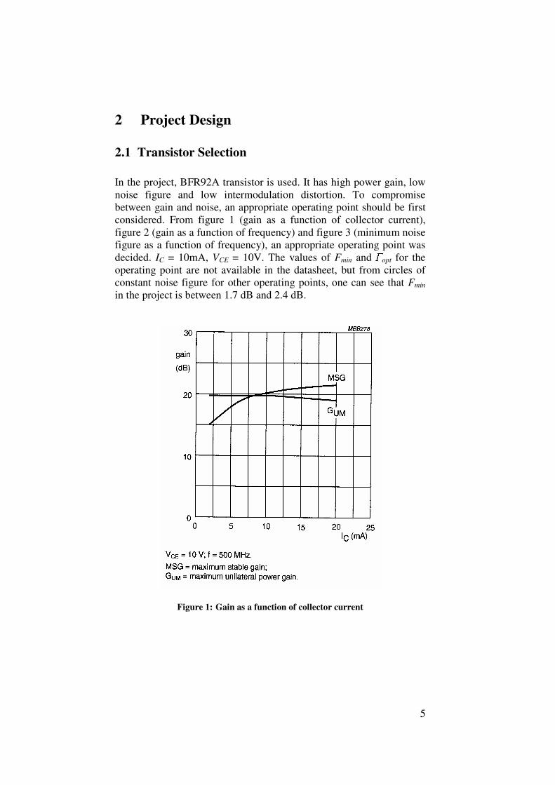
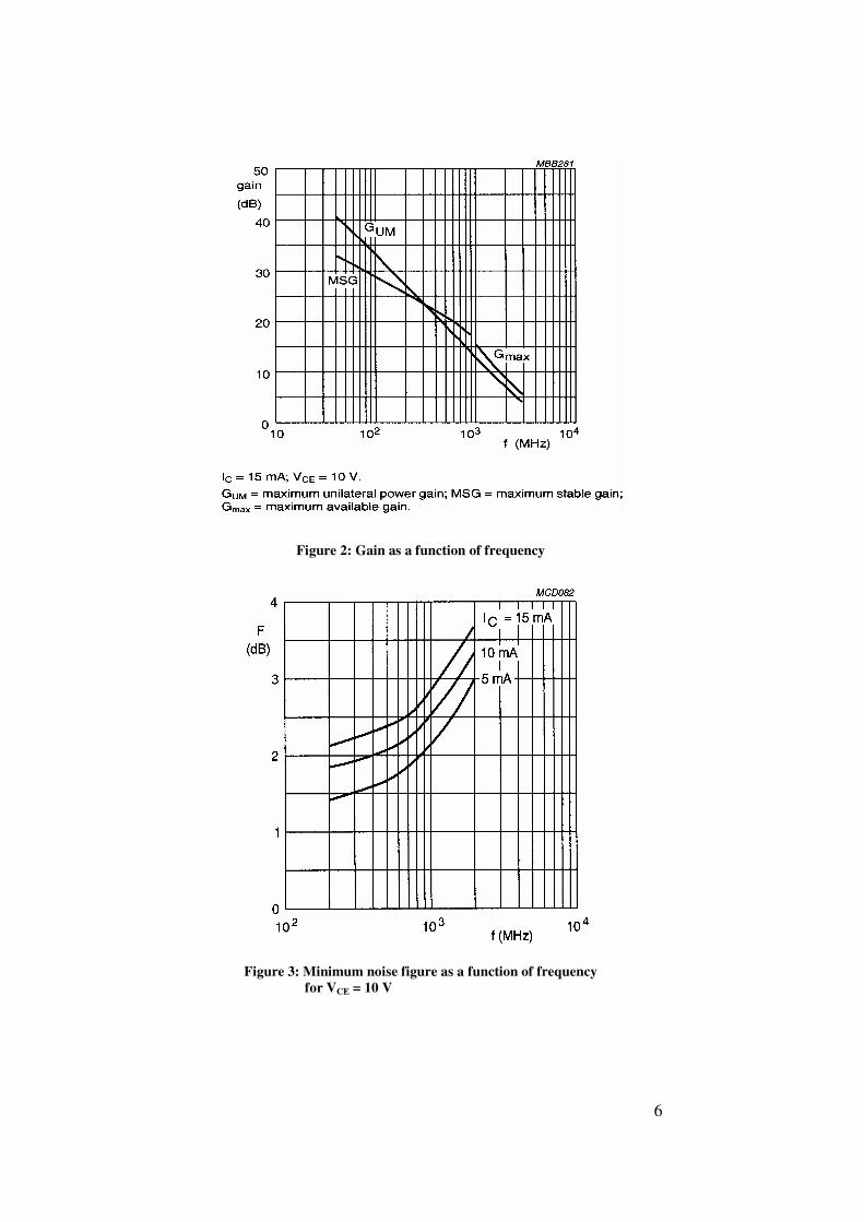
2 Project Design 2.1 Transistor Selection In the project, BFR92A transistor is used. It has high power gain, low noise figure and low intermodulation distortion. To compromise between gain and noise, an appropriate operating point should be first considered. From figure 1 (gain as a function of collector current), figure 2 (gain as a function of frequency) and figure 3 (minimum noise figure as a function of frequency), an appropriate operating point was decided. IC = 10mA, VCE = 10V. The values of Fmin and opt for the operating point are not available in the datasheet, but from circles of constant noise figure for other operating points, one can see that Fmin in the project is between 1.7 dB and 2.4 dB.
Figure 1: Gain as a function of collector current
6
Figure 2: Gain as a function of frequency
Figure 3: Minimum noise figure as a function of frequency for VCE = 10 V

7
2.2 S-Parameters Measurement After the decision of the operating point, the S-parameters of the transistor have been measured. The setup of the measurement is shown in figure 4.
Figure 4: The setup of the S-parameters measurement (page 97 in [2])
From the Network Analyser, one can see the S-parameters from frequency 75 MHz to 150 MHz. The S-parameters diagram is shown in figure 5.
Figure 5: S-parameters of the transistor between 75 MHz and 150 MHz
BFR92A

8
From the S-parameters of the transistor, the stability of the transistor at the operating point can be checked. K = 0.41 and the |∆| = 0.64 at frequency 100 MHz, where ∆ = S11 · S22 – S12 · S21 and K = (1 - |S11|2 - |S22|2 + |∆|2) / (2 · |S12 · S21|). The transistor is only conditionally stable at the operating point, since K < 1. The maximum stable gain is calculated to ensure that the transistor is capable of providing the gain specified above. Since GMSG = |S21 / S12| = 30.22 dB, the gain of the amplifier could be at least |S21|2 = 25.83 dB, so the specification could be fulfilled. 2.3 Property of the Transistor By using Matlab simulation program, the property of the transistor is investigated. The input stability circle and output stability circle are shown in figure 6.
Figure 6: Input stability circle and output stability circle In order to find the stable areas for output and input, the point Γ = 0 is chosen. If ΓS = 0, then ΓL = |S22| < 1. If ΓL = 0, then ΓS = |S11| < 1. The stable areas for input and output can also be found in figure 6. The input amplifier should have high gain and low noise, but the maximum gain is seldom obtained for the same source impedance that gives the minimum noise figure. Compromising between gain and noise figure should be made. Different gain circles are simulated and shown in figure 7.
Input stable area Output stable area

9
Figure 7: Different available gain circles Since Fmin, opt and rn for the operating point are not available in the technical data for BFR92A, some approximation values are chosen to investigate the noise property of the transistor. Fmin = 2.30dB, Γopt = 0.22 + 0.09i, rn = 0.440. Different noise circles are shown in figure 8.
Figure 8: Different noise circles of the transistor
Available gain circle at 25 dB
Available gain circle at 26 dB
Available gain circle at 28 dB
Noise circle at 2.5 dB
Noise circle at 2.9 dB
Noise circle at 4.3 dB Optimal noise point
10
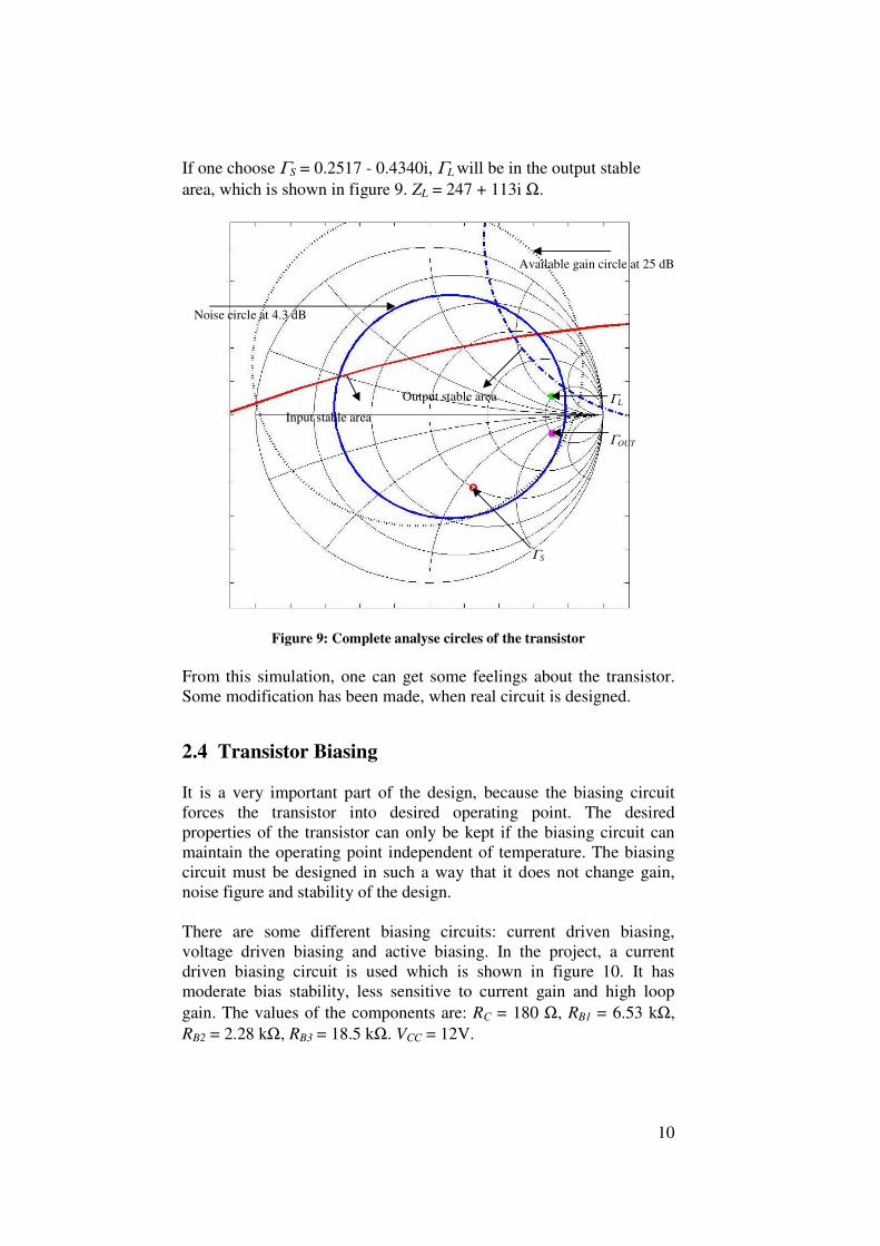
If one choose ΓS = 0.2517 - 0.4340i, ΓL will be in the output stable area, which is shown in figure 9. ZL = 247 + 113i Ω.
Figure 9: Complete analyse circles of the transistor From this simulation, one can get some feelings about the transistor. Some modification has been made, when real circuit is designed.
2.4 Transistor Biasing It is a very important part of the design, because the biasing circuit forces the transistor into desired operating point. The desired properties of the transistor can only be kept if the biasing circuit can maintain the operating point independent of temperature. The biasing circuit must be designed in such a way that it does not change gain, noise figure and stability of the design. There are some different biasing circuits: current driven biasing, voltage driven biasing and active biasing. In the project, a current driven biasing circuit is used which is shown in figure 10. It has moderate bias stability, less sensitive to current gain and high loop gain. The values of the components are: RC = 180 Ω, RB1 = 6.53 kΩ, RB2 = 2.28 kΩ, RB3 = 18.5 kΩ. VCC = 12V.
ΓL
ΓOUT
ΓS
Input stable area
Output stable area
Available gain circle at 25 dB
Noise circle at 4.3 dB

11
BFR92A
RCRB1
VCC +12V
RB3
0
0RB2
Figure 10: Biasing circuit 2.5 Frequency Selection The input amplifier should have high gain in the frequency range 88-108 MHz. It can be realised by using Butterworth or Chebyshev band pass filter, but the order of such filter is very high, if the mirror frequency should be rejected. Such filter can not be used in a real life because of the dominate parasite effects in the components at high frequencies. In the project, a parallel resonant circuit is used to select the frequency, which can be shifted by changing the value of the capacitor. In order to get high Q value, the load is connected to an inductor tap, which is wired at the lab. L = 79.4 nH. C can be changed between 5-56 pF. The parallel resonant circuit with inductor tap is shown in figure 11.
C
0
L
RL
Figure 11: The parallel resonant circuit

12
2.6 Complete Design Circuit The complete circuit is shown in figure 12. In order to isolate the signal design from the bias design, a RFC (radio frequency choke) is used, which provides a high impedance path at high frequencies.
Figure 12: The complete circuit

13
3 Measurement and Result 3.1 Gain Figure 13 shows a measurement of the amplifier circuit with a network analyser from 60 MHz to 160 MHz. In the window showing the parameter S21, there are two markers, one for 88 MHz, which are the resonance frequency that are chosen, and the other is the mirror frequency at 109.4 MHz. This resulted in a difference in gain of 9 dB. In the specification it should have been 20 dB, but it wasn’t possible for this construction to achieve. There was also a change in gain for S21 between different resonance frequencies, which are to be seen in table 1.
Frequency (MHz) Gain S21 (dB) 88 25.3
100 25 108 24.7
Table 1: Gain S21 for different frequency
Figure 13: Result of gain measurement

14
3.2 Compression Point Checking of the design was also made. First there was a measurement of the compression point at different frequencies, 88 MHz, 100 MHz, and 108 MHz, which are to be seen in figure 14, 15, and 16 respectively, and the compression points for the different frequencies can be viewed in table 2. These figures are measured with power sweep in the network analyser.
Frequency (MHz) Compression point (dBm) 88 -9.25
100 -8.75 108 -9.13
Table 2: Compression point for different frequency
Figure 14: Compression point for 88 MHz
Figure 15: Compression point for 100 MHz

15
Figure 16: Compression point for 108 MHz
3.3 Third Order Intercept Point There was also a measuring of the third order intercept point, which was measured with the help of two signal generators a combiner, and a spectrum analyser, which can be viewed in figure 17.
Figure 17: Setup for IIP3 measurement
Two strong signals f1 and f2 with equal magnitude are present in the input of the amplifier. When the two signals are strong enough, 3rd order intermodulation products will be appeared at the frequency 2f1 - f2 and 2f2 - f1, which are shown in figure 18.
.

16
Figure 18: Measurement of the third order interception point
There were two measurements for the intercept points. One is for f1 = 90 MHz, f2 = 89 MHz (figure 19) and another one is for f1 = 102 MHz, f2 = 101 MHz (figure 20), which were made by plotting the output power verses the input power.
Figure 19: Third order intercepts point for 90 or 89 MHz
2f2-f1
f2 f1
2f1-f2
PIN
POUT
f1 or f2
2f1 – f2 or 2f2 – f1
IIP3
f1 = 90 MHz, f2 = 89 MHz
17
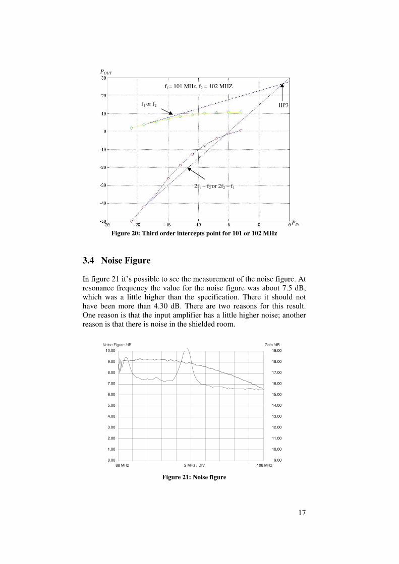
Figure 20: Third order intercepts point for 101 or 102 MHz
3.4 Noise Figure In figure 21 it’s possible to see the measurement of the noise figure. At resonance frequency the value for the noise figure was about 7.5 dB, which was a little higher than the specification. There it should not have been more than 4.30 dB. There are two reasons for this result. One reason is that the input amplifier has a little higher noise; another reason is that there is noise in the shielded room.
0.00
1.00
2.00
3.00
4.00
5.00
6.00
7.00
8.00
9.00
10.00
9.00
10.00
11.00
12.00
13.00
14.00
15.00
16.00
17.00
18.00
19.00
88 MHz 108 MHz 2 MHz / DIV
Noise Figure /dB Gain /dB
Figure 21: Noise figure
PIN
POUT
2f1 – f2 or 2f2 – f1
IIP3
f1= 101 MHz, f2 = 102 MHZ
f1 or f2
18
The amplifier was also tested when an antenna was connected to its input. This gave a good result, because it received a lot of stations, even some stations that are not very strong. There was some noise, but it was not that easy to cancel. 4 Conclusion The functionality of the amplifier was quite good for the FM-band. It was possible to find many different Swedish stations. The gain was as it should be, but the noise was a bit harder to cancel. There were many things that could have been better, like the noise, but the time wasn’t there. The noise parameter for the design was missing, which did it harder to get the best performance. A way to decrease the noise is to choose a lower IC. It should probably be a good thing to have a matching network, but then it was to be iterated into the design. Another way to get a better match is to use a good simulation program and test different values. It was also possible to make the wires shorter. A problem for the design was the magnitude of the mirror frequency rejection, which should have been larger. It can be solved by adding series resonant circuit for mirror frequencies. 5 Acknowledgement We would like to say thank you to Göran Jönsson, who helped us with his knowledge, and also the people from Ericsson, who had helped us with experience from the real life. 6 References [1] L.Sundström, H.Börjesson and G. Jönsson, ”Radio Electronics”, Lund 2001 [2] L.Sundström, L. Durkalec and G. Jönsson , “Radio Electronics, Exercises and Laboratory Experiments”, Lund 2001 [3] L.Sundström and G. Jönsson, ” Radio Electronics Formulas and Tables” , Lund 2001 [4] Philips Semiconductor - Technical Data BFR92A


![ITC 220 MHz Radio Hardware Specifications [FRA]](https://static.fdocuments.in/doc/165x107/6267956bedaae27a392f22b4/itc-220-mhz-radio-hardware-specifications-fra.jpg)