Mechanical Characterization of Polysilicon MEMS: A Hybrid ...

An On-Chip Test Circuit for Characterization of MEMS Resonators
by
John Haeseon Lee
Bachelor of Science, Electrical and Computer Engineering, Cornell University, 2006
Submitted to the Department of Electrical Engineering and Computer Science
in Partial Fulfillment of the Requirements for the Degree of
Master of Science in Electrical Engineering and Computer Science
at the
MASSACHUSETTS INSTITUTE OF TECHNOLOGY
June, 2011
©2011 Massachusetts Institute of Technology All rights reserved.
Author____________________________________________________________
Department of Electrical Engineering and Computer Science May 11, 2011
Certified by________________________________________________________ Duane S. Boning
Professor of Electrical Engineering and Computer Science Thesis Supervisor
Accepted by________________________________________________________
Leslie Kolodziejski Chairman, Department Committee on Graduate Theses

2

3
An On-Chip Test Circuit for Characterization of MEMS Resonators
by
John Haeseon Lee
Submitted to the Department of Electrical Engineering and Computer Science on May 11, 2011 in Partial Fulfillment of the Requirements for the Degree of Master of Science in Electrical Engineering and
Computer Science
Abstract
There has been much interest in developing microelectromechanical systems (MEMS) resonators that achieve comparable performance to traditional resonators yet have smaller footprint and are compatible with CMOS. Recently, MEMS resonators have been proposed that overcome physical limitations in traditional resonators to reach frequencies in the GHz range and that have the potential for compatibility with CMOS, opening up possibilities for new circuits and systems. As with other semiconductor devices, with increasing frequency and with decreasing device size into the submicron scale, variability has started to become a critical issue in MEMS resonators, and thus vigorous characterization of important device parameters has become necessary. This project proposes an on-chip test circuit that can accurately characterize a large number of resonators for variation analysis and is general enough that it can be used with a wide range of resonators, not limited to specific frequencies or other properties. The proposed test circuit is based on a transient impulse response method using a current impulse that excites the resonator under test. The resonator decay behavior is used to accurately measure the series and parallel resonant frequencies and quality factors of the device. The circuit employs a sub-sampling technique that allows measurement and multiplexing of the high-frequency decay signal. A sub-sampling clock generation architecture is proposed that is not based on delay-locked loops, simplifying the design. Finally, a voltage-controlled oscillator (VCO) based analog-to-digital converter (ADC) is implemented on-chip that converts the measured signal into digital codes enabling complete digital interface, which is an important feature for test automation. Simulation shows extraction error less than 100 ppm and 1% for series resonant frequency and series quality factor extraction, respectively.
Thesis Supervisor: Duane S. Boning Title: Professor of Electrical Engineering and Computer Science

4

5
Acknowledgments
I set sail for graduate school almost two years ago with more confidence than was perhaps
warranted and a handful of research ideas that turned out to be not so well defined. Unfortunately, most of
these ideas did not come to fruition and I ended up spending a significant portion of my last two years in
search of an interesting, relevant, and yet realistic research problem. I went through many iterations of
excitement and hope, often followed by disappointment and despair. This roller coaster journey has
finally come to an end and I am extremely excited to present it in this thesis. Though it was painful at
times, I am grateful because what I gained through it is much more than what I set out for.
I would like to express my sincere gratitude to my advisor Professor Duane Boning for his
guidance and support through the many iterations of this project, and for keeping me motivated
throughout. But more than anything, I am especially grateful that he pushed me to be independent even at
times when independence was the last thing I wanted. I would also like to thank Professor Dana
Weinstein for all the discussions and helpful advice throughout this project, and for providing the seed
from which this project has grown.
I would like to thank Dr. Richard Ruby and his colleagues at Avago Technologies, including Drs.
Dong Shim, Steve Gilbert, Maria Guerra and Reed Parker, for the helpful discussions and suggestions,
and for generously providing the FBARs and DSBARs that are used for this test chip. I would like to
thank Dennis Fischette and Dr. Meei-Ling Chiang at Advanced Micro Devices for helpful discussions and
feedback on various aspects of this project from system architecture to detailed circuit designs. I am
extremely fortunate to have them not only as colleagues but also as friends whom I can turn to whenever I
need help.
I would like to thank all my colleagues and friends in the Statistical Metrology Group, Hayden
Taylor, Karthik Balakrishnan, Albert Chang, Wei Fan, Joy Johnson, Li Yu, Jaime Diaz and Cai GoGwilt,

6
for allowing me to be part of this wonderful group. I would especially like to thank the circuit subgroup
for helpful discussions and advice on my research project, courses, as well as life in this lab and at MIT.
I would like to thank my friends in Oori for the practices and performances we had together; they
kept me sane at times when life was not all that rhythmic. I would like to thank my brothers and sisters in
the Park Street Church International Fellowship, Korean small group and the Graduate Christian
Fellowship at MIT for your love and friendship that made my life more real and tangible. Thank you for
your prayers and presence that kept me intact when I wanted to fall apart.
Last but not at all least, I would like to thank my dad and my mom, Dr. Sukhoon and Youngsuk
Lee, and my sister Dr. Hane Lee, for their unconditional love and support that grows stronger and deeper
day by day. Thank you for being there and putting up with me through my countless highs and lows.
Thank you for knowing my heart even better than I do. Thank you that I did not have to say because you
knew already and said for me. Finally, thank you for living the life of following God and Jesus Christ and
showing me that from it comes true joy that is so far beyond anything that this world can ever offer.

7
Table of Contents
1. Introduction ......................................................................................................................................... 15
1.1 Microelectromechanical Systems (MEMS) Resonator ............................................................... 16
1.2 Resonator Operation ................................................................................................................... 19
1.2.1 Quality Factor ..................................................................................................................... 23
1.3 Resonator Modeling .................................................................................................................... 23
1.3.1 Resonances .......................................................................................................................... 25
1.3.2 Series Resistance ................................................................................................................. 25
1.3.3 Effect of Feedthrough Capacitance ..................................................................................... 26
1.4 Variation in MEMS Resonators .................................................................................................. 17
2. Characterization Methodology ............................................................................................................ 29
2.1 Motivation ................................................................................................................................... 29
2.2 Problem Statement ...................................................................................................................... 30
2.3 Existing Characterization Methods ............................................................................................. 31
2.3.1 Vector Network Analyzer ................................................................................................... 31
2.3.2 Frequency Sweep ................................................................................................................ 33
2.3.3 Oscillator ............................................................................................................................. 34
2.3.4 Excitation and Decay .......................................................................................................... 37
2.3.5 Summary ............................................................................................................................. 40
2.4 Proposed Characterization Method ............................................................................................. 41
2.4.1 Decay Signal Processing ..................................................................................................... 41
2.4.2 Multiplexing and Output ..................................................................................................... 43
2.4.3 Excitation ............................................................................................................................ 44
2.5 Model Extraction ........................................................................................................................ 45
3. Test Circuit Design ............................................................................................................................. 49
3.1 High Level Overview .................................................................................................................. 49
3.2 Clock Generation (CG) ............................................................................................................... 51
3.3 Sampling Clock Generation (SCG) ............................................................................................. 52
3.3.1 Ring Oscillator .................................................................................................................... 55
3.3.2 16:1 MUX ........................................................................................................................... 57
3.3.3 Phase Interpolator ............................................................................................................... 57
3.3.4 Edge Select Circuit .............................................................................................................. 58
3.4 Resonator Interface Circuit (RIC) ............................................................................................... 58

8
3.4.1 Excitation Circuit ................................................................................................................ 59
3.4.2 Sensing Circuit .................................................................................................................... 64
3.5 Sampled Voltage Multiplexing (SVMUX) ................................................................................. 70
3.6 Analog-to-Digital converter (ADC) ............................................................................................ 71
3.6.1 Principle .............................................................................................................................. 72
3.6.2 Voltage-Controlled Oscillator Design................................................................................. 74
3.6.3 Multi-phase Counter ........................................................................................................... 76
3.7 Data Interface .............................................................................................................................. 78
4. Post-Processing ................................................................................................................................... 79
4.1 Calibration ................................................................................................................................... 79
4.2 Parameter Extraction ................................................................................................................... 80
4.2.1 Series and Parallel Resonance Measurement ...................................................................... 81
4.2.2 Switch Resistance Measurement ......................................................................................... 82
4.2.3 Feedthrough Capacitance Measurement ............................................................................. 82
4.3 Model Extraction ........................................................................................................................ 83
5. Simulation ........................................................................................................................................... 85
5.1 Block Level Simulation .............................................................................................................. 85
5.2 System Level Behavioral Simulation .......................................................................................... 86
5.3 Simulation Result ........................................................................................................................ 86
6. Summary and Future work .................................................................................................................. 91
6.1 Summary ..................................................................................................................................... 91
6.2 Current and Future Work ............................................................................................................ 91

9
List of Figures
Figure 1-1. Frequency vs. impedance curve of an ideal resonator with a single mode of resonance, with series resonance at 1 GHz: magnitude (top) and phase (bottom). ............................................................... 22
Figure 1-2. Butterworth-Van Dyke model for resonator with single mode of resonance (left) and with spurious modes (right). ............................................................................................................................... 24
Figure 1-3. Two versions of Modified Butterworth-Van Dyke model for resonator with single mode of resonance. The model on the left includes a feedthrough resistance, and the model on the right includes a contact resistance. ....................................................................................................................................... 25
Figure 1-4. Phase of resonator impedance plot showing the effect of feedthrough capacitance. ............... 27
Figure 2-1. Setup for characterization of resonator using a vector network analyzer with microwave probes and high-frequency cables ............................................................................................................... 32
Figure 2-2. Setup for characterization of resonator with the frequency sweep method using a frequency synthesizer and response measurement circuit. .......................................................................................... 33
Figure 2-3. Setup for characterization of resonator using the oscillator method to measure resonant frequency. ................................................................................................................................................... 34
Figure 2-4. Setup for characterization of resonator using the excitation and decay method. Oscillator excites the resonator into steady state and the decay signal is observed. .................................................... 37
Figure 2-5. Signal waveforms describing the principle of the sub-sampling technique. A trigger clock triggers the input signal, which is sampled by the sampling clock. ............................................................ 42
Figure 2-6. Periodic excitation of resonator using voltage steps to allow the use of a sub-sampling technique. .................................................................................................................................................... 44
Figure 2-7. Diagram showing the setup for excitation of series and parallel resonance. On the left is for series resonance and on the right is for parallel resonance. ........................................................................ 45
Figure 2-8. Resonator model including the switch resistance from the test circuit. ................................... 47
Figure 3-1. High level block diagram of the proposed test circuit. ............................................................. 49
Figure 3-2. Clock waveforms showing the operation of the proposed test circuit. ..................................... 50
Figure 3-3. Simplified circuit diagram of clock generation block. ............................................................. 51
Figure 3-4. Simplified circuit diagram of sampling clock generation (SCG) block. .................................. 54
Figure 3-5. Clock waveforms showing the operation of sampling clock generation and principle of edge selection. ..................................................................................................................................................... 54
Figure 3-6. Simplified circuit diagram of 16-stage inverter-based pseudo-differential ring oscillator with enable for sampling clock generation. Circuit diagram of an individual stage (bottom). ........................... 56
Figure 3-7. Simplified circuit diagram showing the state of the oscillator when disabled with value of enabling signals. .......................................................................................................................................... 56
Figure 3-8. Simplified circuit diagram of pseudo-differential 4:1 MUX. ................................................... 57
10
Figure 3-9. Simplified circuit diagram of phase interpolator and clock waveforms showing the principle of operation. ................................................................................................................................................ 58
Figure 3-10. Simplified circuit diagram of edge selection circuit............................................................... 58
Figure 3-11. High level block diagram of resonator interface circuit. ........................................................ 59
Figure 3-12. Simplified circuit diagram of excitation circuit. .................................................................... 59
Figure 3-13. Excitation circuit operation in series resonance measurement mode. .................................... 60
Figure 3-14. Excitation circuit operation in parallel resonance measurement mode. ................................. 61
Figure 3-15. Excitation circuit operation in switch resistance measurement mode. ................................... 62
Figure 3-16. Excitation circuit operation in feedthrough capacitance measurement mode. ....................... 63
Figure 3-17. Excitation circuit operation in disabled mode. ....................................................................... 64
Figure 3-18. Simplified circuit diagram of sensing circuit. ........................................................................ 65
Figure 3-19. Simplified circuit diagram of resonator terminal voltage buffer. ........................................... 67
Figure 3-20. Simplified circuit diagram of sampling head circuit and current-mode buffer. ..................... 68
Figure 3-21. Simplified circuit diagram of sampled voltage multiplexing using current-mode buffer. ..... 71
Figure 3-22. Diagram showing the operating principle of VCO-based ADC. ............................................ 72
Figure 3-23. High level block diagram of VCO architecture. ..................................................................... 74
Figure 3-24. Simplified circuit diagram of V2I and I2I. ............................................................................. 75
Figure 3-25. . Simplified circuit diagram of 16-stage inverter-based pseudo-differential ring oscillator in ADC. Circuit diagram of an individual stage (bottom). .............................................................................. 76
Figure 3-26. Clock waveforms of different VCO clock phases showing states of the ring oscillator. ....... 77
Figure 3-27. Simplified circuit diagram of multi-phase counter in ADC. .................................................. 77
Figure 3-28. Simplified circuit diagram of scan-in and scan-out registers for data interface. .................... 78
Figure 4-1. High level block diagram showing the calibration of signal path and ADC. ........................... 80
Figure 4-2. Diagram showing the resonance measurement parameter extraction process. ........................ 81
Figure 4-3. Diagram showing the feedthrough capacitance measurement parameter extraction method... 83
Figure 4-4. Resonator model including the switch resistance from the test circuit in series and parallel resonance excitation. ................................................................................................................................... 83
Figure 4-5. Diagram showing the model parameter extraction process. ..................................................... 84
Figure 5-1. High level block diagram of MATLB behavioral simulator. ................................................... 86
Figure 5-2. Plot of reconstructed signals for series resonance measurement. Resonator terminal and sampling head output voltage (top) and ADC output code (bottom). ......................................................... 87
Figure 5-3. Plot of reconstructed signals for parallel resonance measurement. Resonator terminal and sampling head output voltage (top) and ADC output code (bottom). ......................................................... 88
Figure 5-4. Plot of reconstructed signals for feedthrough capacitance measurement. Resonator terminal and sampling head output voltage (top) and ADC output code (bottom). .................................................. 88

11
Figure 6-1. High level block diagram of on-chip test circuit interfaced with an array of integrated MEMS resonators. ................................................................................................................................................... 92

12

13
List of Tables
Table 2-1. Summary of existing resonator characterization methods. ........................................................ 41
Table 3-1. Measurement time required for resonators with different series resonant frequency and quality factor. .......................................................................................................................................................... 52
Table 5-1. Summary of model parameter extraction error from behavioral simulation. ............................ 89

14

15
1. Introduction
A resonator is a system that has selective response at a specific frequency or frequencies. These
behaviors are called resonances and the frequencies at which they occur are called resonant frequencies.
The exact behavior at different resonant frequencies may vary depending on the principle of operation,
geometry, material properties, etc., but essentially the system shows a large response when resonance
occurs. Depending on the types of resonators, resonance can occur in many different domains. For
example, a wine glass is a well-known mechanical resonator that can even shatter due to large mechanical
response when excited at its resonant frequency. Other resonance domains include electric,
electromagnetic, acoustic, optical and even molecular, and while the domains in which resonances occur
may differ, the underlying principle is the same.
An electromechanical resonator is another type of resonator, in which actuation and sensing is
done in the electrical domain while resonance occurs in the mechanical domain. Examples of these
devices include quartz crystal resonators, surface acoustic wave (SAW) resonators, and ceramic
resonators; these have been widely used with a long history in a wide range of applications from wrist
watches to the state-of-the-art communication systems. The extremely accurate frequency selectivity of
these devices have allowed the design of low-noise oscillators for the accurate frequency references
necessary for wireless communication circuits as well as for almost any synchronous digital circuits such
as FPGAs, microcontrollers and processors. Also, resonators with high quality factor providing fast cut-
off have been extensively used as filters in the radio front-end [1], so many of which can be found in most
of the billions of cell phones in the world.
Resonators have become an indispensable component for many systems, but despite all the great
benefits, the key drawback is that they cannot be integrated with conventional integrated circuit (IC)
processes because of incompatible materials and processing technology involved with manufacturing
conventional resonators. In most cases, resonators eventually need to be interfaced with ICs, and because

16
they cannot be integrated on the same die, the connections have to be made off-chip either within the
same package or on a printed circuit board (PCB) using wire bond, bump process or PCB wires. These
external connections are far from optimal causing many parasitic effects including inductances from bond
wires and capacitances from large bond pads, which can be detrimental to circuit and system performance,
especially as operating frequency increases and system specifications become more and more stringent.
The fact that resonators cannot be integrated with circuits causes difficult challenges in the effort to
reduce the size and form factor of the overall system; this has become a critical requirement as the size of
electronic systems like cell phones and GPSs become smaller and smaller, while the number of radios in
these systems increases to accommodate a growing number of different communication standards. There
has been much effort in reducing the size of resonators in order to reduce the package size or minimize
precious PCB space usage, and indeed there has been much improvement achieving quartz crystal
resonator and SAW resonators as small as 2.0x1.6 mm2. However, there are physical limits as to how
small these devices can be reduced to, mainly due to manufacturing and handling issues, which make this
problem even more challenging [2]. The area overhead due to external resonators and all the components
required for connection has become a major bottleneck in reducing overall system size, which has been
exacerbated and emphasized even more as IC processing technology advances into very deep submicron
dimensions.
1.1 Microelectromechanical Systems (MEMS) Resonator
In order to solve this issue, there has been much interest in developing microelectromechanical
systems (MEMS) resonators that achieve comparable performance yet have smaller footprint and are
compatible with CMOS processes. Recently, MEMS resonators have been proposed that overcome
physical limitations in traditional resonators to reach frequencies in the GHz range [3]. In addition, they
have the potential for compatibility with CMOS, opening up possibilities for new circuits and systems.
However, so far, there have not been any MEMS resonators developed that can be directly integrated with
CMOS processes. Many MEMS resonators are still discrete components with separate packaging, or they
17
are fabricated on the same die using either MEMS-first or MEMS-last processing [4], but the ultimate
goal is to integrate these devices alongside with circuits, eliminating all the critical drawbacks of the
conventional resonators.
MEMS resonators have already started replacing the conventional resonators and these can be
found even in the product space. One of the best examples is the front-end RF filter and duplexer
components using Film Bulk Acoustic Resonators (FBARs) developed by Avago Technologies that can
be found in most of the current cell phones [5]. FBARs, with smaller size and comparable performance,
have partially replaced SAW resonators that have been traditionally used for this type of filter
applications. Also, recently frequency references and frequency synthesizers have been developed and
already sold; these products use MEMS resonators and achieve similar performance as ones with quartz
crystal resonators [2] [6] [7], demonstrating that MEMS resonators are not only viable candidates for
replacing conventional resonators but also for further improving the circuits and systems for next
generation applications.
1.2 Variation in MEMS Resonators
As with other semiconductor devices, MEMS resonators are susceptible to variation not only due
to process but also due to environment and aging; because of the stringent requirements of the
applications for MEMS resonators, these variations are becoming a critical issue that needs more attention.
In particular, as the size of MEMS resonators decreases into the submicron scale in an effort to achieve
higher frequency and smaller system size, variation due to fabrication and processing is becoming more
troublesome.
MEMS process and various steps involved in fabrication are inherently similar to conventional
CMOS or other semiconductor fabrication processes and because of this similarity they also share some
common sources of process related variation. These include line width and line space variation from
lithography and etching, and metal and dielectric thickness variation from deposition and polishing [10]

18
[11]. Variation in geometry itself translates to severe variation in performance and functionality, but in
the case of MEMS resonators, material properties such as Young’s modulus and piezoelectric coefficient,
which depend heavily on various processing steps, also play a significant role and as a result, worsen the
overall variability of the device. In frequency reference applications, which have some of the most
stringent requirements, resonant frequency needs to be controlled in the order of parts-per-million (ppm),
while geometric and material properties variation from fabrication can be up to a few percent [12] [13].
Techniques such as trimming [14] [15] are used to address these issues. Equally important is accurate
characterization of variability in the device, which can lead to better process control strategies,
development of post-fabrication trimming methods, as well as enabling variation aware design and
development of circuits and systems.
Besides process variation, environmental variations in ambient temperature and other operating
conditions are also a significant concern. Again, some of the high-performance frequency reference
applications require single-digit ppm variation in frequency over greater than 100 °C range of temperature
[1]. Some studies have been done to look at the temperature stability of MEMS resonators [16] [17] [3],
and temperature compensation designs and methods have been developed [18] [19] [20], but compared to
the conventional resonator counterpart, performance is still inferior. Another variation related issue that
deserves careful attention is aging, especially because MEMS resonators involve actual moving parts.
Studies have been done to look at MEMS resonator resonance frequency drift over a long period of time
to see the effect of aging [3]; however, at least for the tested device structure, aging has been found to be
negligible.
What makes the issue of variability in MEMS resonators even more challenging is that even
though the fabrication processes and thus the main sources of variation are inherently similar between
different types of resonator, the effect of variation can be quite different because of the differences in
operating principles. Because of this difference, understanding variability of one type of resonator does
not necessarily provide valid information about another type of resonator.

19
In order to address the aforementioned variability issues with MEMS resonators, a viable
characterization methodology is necessary that can be used to characterize statistical distribution of
variation associated with critical parameters. The conventional characterization methods that are currently
used have challenges that must be overcome and, especially with the integrated resonators, new
challenges have arisen that make characterization even more difficult. These will be covered in the
following chapter.
1.3 Organization of Thesis
This thesis is organized as follows. In Chapter 2, resonator operation and modeling are discussed,
and important parameters are introduced and derived. Resonator characterization methods are discussed
in Chapter 3. First, the existing methods are explained and the weaknesses that prohibit the use of
particular methods are discussed. A new characterization method is then proposed and some of the key
issues with the method are discussed. In Chapter 4, a test circuit implementing the proposed
characterization method is covered in detail, from overall system architecture and operation, to detailed
design of individual circuit blocks. In Chapter 5, post-processing issues such as calibration and extraction
are discussed, followed by simulation and results which are covered in Chapter 6. Finally, in Chapter 7 a
summary of this thesis is provided, which is followed by work currently on-going and planned to be done
in the future.

20

21
2. Resonator Operation and Modeling
In this chapter, resonator operation and modeling are described, as well as a number of key
parameters that are necessary in understanding both the device operation and issues associated with
characterization. First, basic resonator operation is described, with explanation of resonator impedance,
resonant frequencies and quality factor. Second, different models that are used for resonator modeling are
described, and key parameters introduced and derived.
2.1 Resonator Operation
A resonator is usually a two terminal device, though not necessarily symmetric. The terminals are
used to actuate and sense the device response in whatever domain the device operates in. For example,
most MEMS resonators, including FBARs, are electromechanical resonators, where actuation and sensing
occurs in the electrical domain through capacitive, piezoelectric, piezoresistive, or other physical effects.
Resonance can also occur in the mechanical domain through vibration of structures such as cantilever
beams, thin films, bars, or other mechanical elements. Resonance occurs because one or more standing
waves form within the device, whose properties such as frequency, amplitude and phase are dictated by
the geometry or material properties of the device.
In a typical resonator, regardless of the resonance domain, more than one resonance exists at
different frequencies. These are called modes of resonance. Different modes exist because often there are
multiple ways that standing waves can form in the device and there can be multiple harmonics associated
with each resonance. However, due to dissipations within the device, many of the modes have very weak
energy, while a few that have significant energy stand out. Also, it is a goal of the resonator designers to
purposely suppress unwanted modes, called spurious modes, while maximizing the strength of the modes
that are desired, by cleverly addressing the means of dissipation, such as friction, surface losses, and
anchor losses. In this thesis, we will focus on electrical and electromechanical resonators, where electrical
impedance is the primary parameter of interest.

22
Each resonance mode is associated with two resonances, namely, series resonance and parallel
resonance. Series resonance always occurs at a lower frequency than the parallel resonance, and is
characterized by the impedance of the device reaching a local minimum. When series resonance occurs,
current into the device reaches a local maximum, thus behaving close to a short circuit. Parallel resonance
occurs at slightly higher frequency and the impedance of the device reaches a local maximum. In this case,
current into the device reaches a local minimum, thus behaving close to an open circuit. Parallel
resonance exists because of the feedthrough capacitance between the two terminals of the device. Figure
2-1 shows frequency vs. impedance curve of an ideal resonator with a single mode of resonance. The
impedance curve looks capacitive in the frequency range below and above the resonance, which is due to
the feedthrough capacitance. The two peaks, downward and upward, observed around resonance
correspond to series resonance and parallel resonance, respectively.
Figure 2-1. Frequency vs. impedance curve of an ideal resonator with a single mode of resonance, with series resonance at 1 GHz: magnitude (top) and phase (bottom).

23
2.1.1 Quality Factor
One of the key parameters of a resonator besides resonant frequencies is quality factor,
sometimes abbreviated as Q factor or Q. There are many ways to define quality factor, but the most
fundamental definition is given in (2.1) [8].
2
(2.1)
As (2.1) states, quality factor is a scaled ratio between stored energy and dissipated energy per cycle.
Thus, it gives a measure of how much energy is lost every cycle if energy is injected into a system;
because it is measured per cycle, quality factor is always associated with frequency. Theoretically, quality
factor can be calculated for every frequency, but in typical practice, it is defined in relation to a specific
resonance. In the case of a resonator, high quality factor means that when the device is excited into
resonance, it takes many cycles for the standing wave to disappear. Since quality factor is related to
resonance, both series and parallel resonance have quality factors associated with them, namely, series
quality factor and parallel quality factor.
There is another way to definition of quality factor; though it is not as general as (2.1), it is a little
more intuitive. For systems with high quality factor, (2.2) can be used to interpret the quality factor as a
ratio between resonant frequency and bandwidth [8]. Thus, from the impedance curve, the higher the
quality factor, the narrower is the peak at resonance.
Δ
(2.2)
2.2 Resonator Modeling
Resonators are traditionally modeled using the Butterworth-Van Dyke (BVD) model as shown on
the left side of Figure 2-2. A series RLC branch formed by series resistance (Rs), motional inductance (Lx)
and motional capacitance (Cx) models the series resonance of the device. This RLC branch is not a

24
physical model, but rather is an equivalent circuit model of the mechanical resonance that occurs in the
device, hence the term motional. The electrical resonance arising from Lx and Cx model the resonance
behavior of the resonator, and the electrical dissipation through Rs models the energy dissipation
occurring in the device through various means. During series resonance, the impedance of Lx and Cx
cancel each other out leaving only Rs, thus the RLC branch looks purely resistive at resonance with
resistance equal to Rs. A capacitor (Co) models the feedthrough capacitance between the two terminals,
and the two shunt capacitors (CL1 and CL2) model the capacitance between each contact to ground. This
BVD model with seven components models a resonator with a single resonance mode and the series and
parallel resonances associated with it. In order to model spurious modes, multiple RLC branches are used
in parallel with the main RLC branch as shown on the right side of Figure 2-2.
Figure 2-2. Butterworth-Van Dyke model for resonator with single mode of resonance (left) and with spurious modes (right).
For some resonators, a slightly modified model called the Modified Butterworth-Van Dyke
(MBVD) model is used, two versions of which are shown in Figure 2-3 [9]. There are a number of
different versions of MBVD models, but, as shown on the left side of Figure 2-3, the main difference is
the resistance in series with the feedthrough capacitor that models the degradation in parallel quality
factor compared to series quality factor. In some cases, a different version of MBVD model is also used,
shown on the right side of Figure 2-3, where a resistance is placed in series with the previous model in
order to model the resistance of the contact, which further degrades series quality factor.

25
Figure 2-3. Two versions of Modified Butterworth-Van Dyke model for resonator with single mode of resonance. The model on the left includes a feedthrough resistance, and the model on the right includes a
contact resistance.
2.2.1 Resonances
From the BVD model, resonant frequency and quality factor of series and parallel resonance
modes can be analytically derived as shown in (2.3), (2.4), (2.5) and (2.6). Here fs and Qs denote the series
resonant frequency and series quality factor, respectively, and fp and Qp denote the parallel resonant
frequency and parallel quality factor, respectively.
12
1
(2.3)
1
(2.4)
12
1
(2.5)
1
(2.6)
2.2.2 Series Resistance
Another key parameter often mentioned with regard to resonators is the series resistance. This
parameter is sometimes also referred to as motional impedance or resonator impedance, and it denotes the
impedance of the device seen between the two terminals at series resonance when the device impedance
reaches minimum. This is modeled by the resistor Rs in the BVD model. Series resistance is an important
26
parameter because it represents the amount of energy lost in the device at resonance. In applications such
as oscillators, series resistance indicates how much gain is required in order to overcome the loss caused
by the resonator. Series resistance depends on many different factors such as resonance domain,
architecture, size, material properties. For this reason, it is often used as a way to classify different types
of resonators: low-impedance, medium-impedance and high-impedance.
This classification is not a clear cut one, but low-impedance typically refers to 1 – 100s Ω of
impedance while high-impedance refers to 10s – 100s kΩ, and between these is referred to as medium-
impedance. This classification is an important one especially in deciding on circuit architecture and ways
to interface with the device. For low-impedance resonators, connecting resistive elements severely
degrades the quality factor of the device, while for high-impedance resonators, connecting additional
capacitance between its terminals can cause even functional failures. This is described in more detail in
the design of sensing circuits in Section 4.4.2.
2.2.3 Effect of Feedthrough Capacitance
Feedthrough capacitance is a physical capacitance formed by the terminal contacts and associated
metals. It provides an electrical path between the two terminals of the device in addition to the resonance
branch and is modeled by Co in the BVD model. As mentioned previously, this is why the impedance
curve looks capacitive away from the resonance. Because the feedthrough capacitance is in parallel with
the series resonance branch, it provides an additional current path between the terminals that takes current
away from the resonance branch, which is equivalent to weakening the strength of resonance. If a device
is correctly designed, impedance of the feedthrough capacitance at resonance should be much larger than
impedance of the resonance branch, such that the majority of the current goes through the resonance
branch and not through the capacitance. This is why low-impedance resonators can accommodate larger
feedthrough capacitance than high-impedance ones. However, if there is excessive amount of feedthrough
capacitance, more current flows through the capacitor than through the resonance branch, and the device
no longer behaves as a resonator but instead as a capacitor. This can be clearly seen by observing the

27
phase plot of the resonator impedance as the size of the feedthrough capacitance is swept, as shown in
Figure 2-4.
Figure 2-4. Phase of resonator impedance plot showing the effect of feedthrough capacitance.
As can be seen from the plot, as Co increases, the maximum phase of the impedance decreases from close
to 90° to below 0°, at which point resonance is no longer detected. Maximum Co allowed for a given
resonator can be analytically derived by setting the maximum phase of the impedance to 0°. Derivation is
shown in (2.7) and (2.8).
angle Z tanwL
1wC
Rtan
wR C
1 wC wL1wC
(2.7)
C
1R
1wQ 2w
≅1R
12w
(2.8)

28

29
3. Characterization Methodology
This chapter discusses characterization methods relevant to resonator characterization. First, the
existing methods are described in detail with their strengths and weaknesses. Second, a new method is
proposed that is appropriate for integrated MEMS resonator characterization, which is followed by
detailed discussion of a number of key issues associated with the proposed method.
3.1 Motivation
As described in Chapter 1, MEMS resonators offer many advantages over conventional
resonators. Their smaller area, comparable or even superior performance in certain aspects, and the
possibility of integration with IC processes provide the possibility of not only replacing conventional
resonators but also enabling different circuit and system architectures that were not possible with previous
counterparts. The possible applications of MEMS resonators include low-noise oscillators, and high-Q
filters used in RF radio front-ends that require extremely precise control of resonator parameters, often
even more stringent than for CMOS devices. As MEMS resonators scale down in size in order to meet the
performance requirements and ever decreasing system area requirements, variability in resonators has
started to become a critical issue.
This has brought up a need for better understanding and characterization of variation in critical
resonator parameters, which can be used in an effort to reduce variation as well as to develop robust and
novel circuit and system designs. For accurate characterization of variation, large numbers of
measurements of devices are necessary to achieve statistical confidence. The conventional
characterization method of using a network analyzer satisfactorily provides accurate measurement of
devices, but this method requires a rather slow testing process that is analog in nature, and requires a large
instrument that is bulky and costly. Also, it requires multiple probe pads for each device, which may not
be an issue for the conventional resonators and even for the existing discrete MEMS resonators, but can
be a critical issue for the future integrated MEMS resonators that most likely will not require probe pads

30
if not for the sole purpose of characterization. Integrated devices benefit from not having probe pads
because of reduced parasitic inductance and capacitance and smaller overall area, but if probe pads are
added just so that individual devices can be characterized, such resonators lose many of the benefits of
integration. In some cases, parasitic effects from having probe pads can severely affect the device
performance or even cause functional failures. These issues call for a different characterization method
that can provide accurate and efficient measurement of integrated devices necessary for both individual
device characterization as well as characterization of variability associated with the device.
3.2 Problem Statement
It is clear from the issues described in the previous section that for future integrated MEMS
resonators, a new characterization method is required to meet the needs of the device, circuit and system
designers. There are two main requirements that need to be satisfied. First, the characterization method
needs to be accurate and fast. The accuracy requirement depends on various factors and applications, such
as whether the characterization is for an individual device for the characterization of performances, or for
a large number of devices for the characterization of variation. For characterization of performance,
accuracy in the ppm range is required for some applications, which can be achieved using conventional
methods, but because of the extreme accuracy required, it can still be very challenging. For the
characterization of variation, accuracy needs to be well below the expected amount of variation, but the
requirement can be often relaxed compared to the previous case. Second, for the new method to be used
with integrated resonators, it cannot require probe pads, which means that it has to be integrated on-chip
with the resonators such that measurement is done inside the chip. Since the measurement circuit is on-
chip, area of the circuit becomes an important requirement, which in many cases is related to the accuracy.
So the tradeoff between accuracy and area needs to be considered carefully in the design process. This
also leads to another important requirement, which is the ability to multiplex and characterize so that as
much as possible the measurement related circuits are shared. This is not only beneficial for minimizing
area, but also for reducing the variation caused by the measurement related circuits.

31
To summarize, a new characterization method is required, that is accurate, fast and is
implemented on-chip, thus removing the need for probe pads, yet area-efficient such that the overhead of
the measurement circuit is minimal. In the following sections, existing characterization methods are
reviewed analyzing the strengths and weaknesses of each method, after which, a method is proposed that
meets the requirements described above.
3.3 Existing Characterization Methods
There are many different methods that have been used for characterization of resonators. In
general, all characterization methods entail some kind of excitation of the device and sensing of the
output response either in the time domain or frequency domain. Different methods have strengths and
weaknesses making one more suitable for a specific application over the other. In this section, first,
characterization of resonators using a vector network analyzer, which is the most conventional method, is
described and analyzed, providing reasons why it is not a good method for characterizing integrated
MEMS resonators. Then a few specific methods that have been proposed to characterize resonators are
analyzed and evaluated in detail, to see if they are suitable for characterization of integrated MEMS
resonators. The most significant points for evaluation are whether the method can be implemented on-
chip or not, whether the method of excitation and sensing is practical and implementable, and whether the
measurement can be multiplexed allowing the sharing of measurement circuits. The characterization
methods covered in this section are the vector network analyzer method, a frequency sweep method, an
oscillator loop method, and an excitation and decay method.
3.3.1 Vector Network Analyzer
Use of a vector Network Analyzer (VNA) is the most conventional and the most accurate method
available for high-frequency characterization. It is extensively used for characterization of devices and
passives including transistors, resonators, inductors, etc., and characterization time is rather slow. A VNA
operates in the frequency domain by sweeping the input frequency and observing the output response at

32
the input frequency. It requires high-frequency probes, often requiring ground-signal-ground (GSG) probe
pads for each signal for signal integrity reasons. In order to eliminate the effect of the cables and the
probes, careful calibration before measurement is necessary.
Figure 3-1. Setup for characterization of resonator using a vector network analyzer with microwave probes and high-frequency cables
Resonators are usually two terminal devices, thus it requires six probe pads for characterization of
one resonator as shown in Figure 3-1, though in some cases ground pads are used as the second terminal,
thus requiring two or three pads per resonator. But in some cases, extra DC biases are needed, in which
case, even more than six probe pads can be required per resonator. Each probe pad can be as large as 50
um x 50 um to 100 um x 100 um, and with three to six of these for each resonator, the area overhead can
be extreme, especially as resonators are approaching micron or even submicron scale. For integrated
MEMS resonators, this can be a critical issue especially for the characterization of variation, which
requires measurement of a large number of devices. Large pad area required for probing will ultimately
limit the number of devices that can be characterized on a given chip. Another issue with probe pads is
the unnecessary parasitic effects from the pads themselves and associated metal routings within the chip.
Parasitic effects are especially troublesome because they cannot be removed with conventional calibration
methods; though there are some ways that have been proposed to get around this, it is still challenging
and accuracy of measurement is compromised. For integrated resonators where probe pads are not
necessary for functional reasons because the connections with circuits are made within the chip, having

33
probe pads for the sole purpose of characterization can be detrimental to the performance of the circuit
even to a point of functional failure.
The VNA is an indispensable tool for high-frequency characterization and it serves as almost a
golden standard to other methods of characterization because of its accuracy. However, the requirement
of probe pads disqualifies this method as a suitable method of characterization of integrated MEMS
resonators.
3.3.2 Frequency Sweep
The principle of the frequency sweep method is essentially the same as in a VNA, except that the
significant part of the measurement structure is implemented on-chip as shown in Figure 3-2. As in a
VNA, a single-tone frequency source, which is swept in frequency, drives the resonators and the output
response at the input frequency is observed [21] [22] [23]. The input frequency source is either created
within the chip using a frequency synthesizer or created off-chip and brought in. Sensing of the output
response also has been done both on-chip using an envelope detector or off-chip using a scope.
Figure 3-2. Setup for characterization of resonator with the frequency sweep method using a frequency synthesizer and response measurement circuit.
There are a number of issues with this method that disqualifies it as a suitable method for
integrated MEMS resonators. First, this method is somewhat limited to low-frequency characterization
because of the challenges in creating a high-frequency source. Creating a low-noise high-frequency
source with extremely fine resolution that can be precisely controlled is an extremely challenging task,
part of the reason why VNAs are so bulky and costly. Especially for resonators with high Q, the

34
frequency sweep needs to be done in very fine resolution to accurately capture the response curve. For
example, to characterize a 1 GHz resonator with quality factor exceeding 1000, frequency resolution of
well below 1 MHz is required and it needs to be controlled precisely. Creating this source on chip in an
area-efficient fashion is extremely challenging. Also, even after assuming that this frequency source can
be created, routing this high-speed signal without distortion around the chip to characterize a large
number of devices is not practical.
Second, sensing the output response is also challenging for both on-chip and off-chip cases. In the
on-chip case, high-speed linear analog circuit blocks are required to accurately sense the output; these are
challenging to design and often consume large area. Sensing circuits can be shared among a number of
resonators, but multiplexing and routing high-frequency resonator output responses requires high-speed
linear buffers, pushing the design and variability problem to a different place that is equally difficult to
solve. In the off-chip case, there is a similar problem even though the sensing circuit is not required,
because high-speed linear buffers are still necessary to send resonator output responses off-chip. Also,
measuring the signal off-chip almost defeats the purpose of doing an on-chip characterization, as the
analog blocks and multiplexing structure can easily exceed the area required for probe pads.
To summarize, because of the challenges in implementing the excitation and sensing circuits for
the frequency sweep method, it is not a practical method for integrated MEMS resonator characterization,
especially for the purpose of characterization of variation.
3.3.3 Oscillator
Figure 3-3. Setup for characterization of resonator using the oscillator method to measure resonant frequency.

35
An oscillator loop has also been used to characterize resonators by measuring the frequency of
the oscillator either digitally on-chip using dividers and counters, or off-chip using an oscilloscope or a
spectrum analyzer as shown in Figure 3-3 [24]. Depending on the topology, either series resonant
oscillator or parallel resonant oscillator can be designed; in each case, a different resonator parameter is
measured. For measurement of a large number of devices, either each resonator can have its own
oscillator loop or a multiple of resonators can share a common oscillator loop, but sharing common
circuitry can be problematic due to parasitic loading, especially for high-frequency resonators.
There are a number of key strengths to this method. First, the measurement circuit required for
this method is fairly simple allowing them to be easily integrated on-chip with the resonators, thus
eliminating the need for probe pads. Second, the “self-excitation” carried out by the oscillator loop with
the resonator itself doing the frequency selection is a huge advantage and a much simpler method
compared to the frequency-domain characterization method where frequency is swept. Third, sensing of
the frequency is done in the digital-domain using dividers and counters, which is much simpler and robust
compared to methods that require high-speed linear analog blocks. Finally, digital-domain sensing makes
it possible to do multiplexing, which is another key requirement.
However, there are also a number of critical weaknesses. First, the simplicity of the measurement
circuit comes at the cost of its accuracy. In the case of a series resonant oscillator topology, even though
the loop oscillates close to the series resonant frequency, it is not exactly at the resonant frequency. This
is because the circuit in the oscillator loop contributes nonzero phase shift, especially in the case of high-
frequency resonators, which forces the loop to oscillator at slightly lower than the series resonant
frequency. This may not be too much of an issue for high-Q resonators, because the offset frequency
required to meet the zero-phase requirement for oscillation can be very small, in the ppm range. However,
high-Q resonators are usually used for application requiring extremely precise control of frequency, thus
characterization error even in the ppm range may pose an issue. In the case of a parallel resonant
oscillator topology, the oscillation occurs at the parallel resonance and the frequency depends on the

36
feedthrough capacitance, which is a combination of resonator intrinsic feedthrough capacitance,
capacitance from pads, and parasitic capacitance from the circuits in the oscillator loop. Thus, the exact
capacitance associated with parallel resonance is unknown unless separately measured. Even though in
many resonators parallel resonance occurs very close in frequency to series resonance, knowing the
parallel resonance and even the feedthrough capacitance does not provide enough information to ascertain
the exact series resonant frequency.
Second, the oscillator loop has to be carefully designed for each resonator type to ensure that
oscillation occurs. This may be a trivial task for low-frequency resonators, but for high-frequency
resonators, this can be very challenging. Also for high-impedance resonators, the oscillator circuit is quite
large in order to provide enough gain to overcome the loss in the resonator, which leads to large area
consumption by the oscillator circuit and poses challenges to having one oscillator loop for each resonator.
Sharing a common oscillator loop may help in this case, but as mentioned earlier, even this can be
troublesome due to excessive parasitic loading, especially for high-frequency resonators.
The last and perhaps most significant issue is the fact that oscillator can only provide very limited
information, i.e. approximate resonant frequency. This is actually related to one of the strengths of this
method, which is the convenience in sensing because it only requires measurement of frequency in the
digital domain. However, because the signal is digital, information related to the resonance other than
frequency, such as quality factor has been shadowed and cannot be extracted. This is exactly the reason
why sensing is so difficult in other methods because in those cases, additional information is being
extracted, which poses additional requirements such as linearity on the measurement circuit.
There has been previous work that showed that information regarding quality factor can be
attained even with an oscillator loop approach, but it is only relative information between resonators
while the absolute value cannot be extracted. The proposed method in [24] utilized the fact that the
oscillation amplitude is a function of the resonator quality factor and by observing it, information

37
regarding resonator quality factor can be obtained. However, the relationship between oscillation
amplitude and resonator quality factor is not at all a simple linear relationship, but rather a complex
function involving the effect of the oscillator loop as well, making it difficult, if not impossible, to extract
quality factor accurately from oscillation amplitude alone.
Even though the oscillator loop method may not provide enough accuracy for it to be used for
applications that require extremely accurate characterization, it still is an attractive option because of its
simplicity, and the possibility of integration for certain applications where simple on-chip characterization
is necessary while the accuracy requirement can be relaxed. However, for the purpose of characterizing
variation in high frequency integrated MEMS resonators, this method is not a viable one.
3.3.4 Excitation and Decay
The last method to be evaluated is the excitation and decay method, as shown in Figure 3-4 [25]
[26] [27].
Figure 3-4. Setup for characterization of resonator using the excitation and decay method. Oscillator excites the resonator into steady state and the decay signal is observed.
In this method, initially the resonator is connected to an oscillator loop and the loop is oscillating. Once it
reaches steady state, the loop is opened and lets the energy in the resonator decay as it continues to
oscillate. This decay signal can be expressed as a sinusoid with exponential decay envelope as given in

38
(3.1), where fosc and τ denote the decay oscillation frequency and decay envelop time constant,
respectively. Both parameters are function of resonant frequency (fo) and quality factor (Q) as in (3.2) and
(3.3).
/ cos 2 (3.1)
4
(3.2)
(3.3)
From the decay signal, fosc and τ can be extracted easily and once they are known, both fo and Q can also
be calculated, which in turn can be used to extract the model parameters described in Section 2.2.
There are a number of strengths to this method that make it a good candidate for characterization
of integrated MEMS resonators. First, as in the oscillator method, the simplicity of the excitation method
is a significant advantage. By using an oscillator, the resonator is automatically excited near its resonant
frequency, thus eliminating the need for an accurate low-noise high-frequency source. The second and
perhaps most significant strength is the capability to extract key parameters, specifically the resonant
frequency and quality factor, in a simple manner from a transient signal. In the frequency-domain
methods, the most difficult challenge is sweeping the input frequency in fine enough resolution to
accurately characterize the resonator response around its resonant frequency. Since the higher the quality
factor, the narrower the peak in the response, for high-Q resonators, the frequency sweep needs to be done
in very fine resolution, making it even more challenging. Thus, in frequency-domain methods, the
measurement accuracy drops as quality factor increases. However, in the excitation and decay method,
because the decay envelope time constant increases with quality factor, it takes a longer time for resonator
energy decay, thus providing more data points to be used for extraction of fosc and τ, resulting in more
accurate extraction of fo and Q. This is an extremely desirable trait of this characterization method,

39
especially because in general, the applications that utilize high-Q resonators demand more accurate
characterization of the device parameters.
However, this method still has a number of weaknesses that need to be addressed. First, as
mentioned for the oscillator loop method, the excitation method using an oscillator suffers from the fact
that a custom oscillator has to be designed, which can be troublesome especially for high-frequency
resonators. A more severe issue is the sensing and measuring of the decay signal. As can be seen from
(3.1), the decay signal oscillates near the resonant frequency, which can be in the GHz range for advanced
resonators and this signal needs to be processed either on-chip or off-chip to extract fosc and τ. In previous
works, both on-chip and off-chip methods have been demonstrated, though both methods still have issues
that prevent them from being ideal candidates for on-chip resonator characterization, as summarized
before.
The off-chip method was demonstrated in [25] for characterizing a quartz crystal resonator with
resonant frequency of 10 MHz by sending the decay signal off-chip and capturing it using an oscilloscope.
The captured signal was fit using the model shown in (3.1) and fosc and τ were extracted. In this method,
the key issue is the buffering of the decay signal so that it can be sent off-chip for two reasons. First, the
buffer needs to drive a significant amount of capacitance, which includes the pad capacitance, the
capacitance from routing both on-chip and off-chip, and the capacitance from the oscilloscope probe. For
low-frequency resonators such as what was used in this work, this may have been feasible, though it
would have required a large buffer. However, for high-frequency resonators in the GHz range, this is not
at all a trivial issue. Designing a buffer that can drive a large load at such high frequency is extremely
challenging and even if it is feasible, the area required for this buffer may be unacceptably large. This is
especially troublesome in the context of characterization of a large number of resonators, where area
overhead is one of the key issues. In this case, requiring a large buffer for each resonator is not an
acceptable solution. Multiplexing the decay signal from the resonators and using a single buffer that
drives it off-chip may be a way to solve this issue, but as in the case for the frequency sweep method,

40
multiplexing high-frequency signals is challenging in itself, not to mention requiring high-speed buffers
in the multiplexing structure. So far, only the aspect of driving the load has been discussed; however,
there is another issue that makes the problem even more challenging: the linearity requirement for the
buffer. Since the decay envelope time constant has to be extracted from the curve, it requires linear signal
processing of the decay signal, thus requiring a high-speed linear voltage buffer, which is extremely
challenging.
The on-chip method was demonstrated in [27] also for characterizing a quartz crystal resonator,
in this case for a much lower frequency of 10 kHz, by using an on-chip envelope detector to capture the
envelope of the decay signal. In this work, the decay envelope time constant was even calculated on chip
by looking at the ratio between two peak values. It was possible for this case because the frequency was
so low, but for high-frequency characterization, the same issues arise with this method as for the off-chip
method. Though there are many different ways to implement an envelope detector, designing a high-
speed linear envelope detector is very challenging often requiring large passive components. As in the
off-chip method, using a large envelope detector for each resonator is not acceptable and neither is the
multiplexing method for the same reason described previously.
3.3.5 Summary
To summarize, the comparison of several existing characterization methods are shown in Table
3-1. Of these, the excitation and decay method is an attractive candidate especially because of the simple
yet accurate extraction method. Though the decay signal sensing method of previous implementations had
issues that must be addressed, with a different approach that works for the integrated MEMS resonator,
this method has the most potential compared to the other methods.

41
Method Integration Parameter Measurement Implementation Network Analyzer
Cannot be integrated Series resonant frequency and quality factor and parallel resonant frequency and quality factor can be measured.
Most accurate method of measuring.
Cannot be implemented on-chip
Frequency Sweep
Can be fully or partially integrated
Series resonant frequency and quality factor and parallel resonant frequency and quality factor can be measured.
Accuracy degraded for high Q resonators.
Implementation has been demonstrated
Frequency synthesis block is extremely difficult to implement on-chip
Not very practical Oscillator
Loop Can be integrated For a given oscillator topology, only
resonant frequency (but not exact) of one mode is measured.
Absolute quality factor value cannot be measured.
Medium accuracy
Easy to implement on-chip
Oscillator loop needs to be specially designed for each resonator type
Excitation and Decay
Can be integrated Resonant frequency and quality factor of series and parallel modes
High accuracy
Fairly easy to implement on-chip
Table 3-1. Summary of existing resonator characterization methods.
3.4 Proposed Characterization Method
After analyzing and comparing the strengths and the weaknesses of each characterization method,
a modified excitation and decay method was chosen for the work here. As discussed in Section 3.3.4, the
major strength of the excitation and decay method is the ability to extract parameters from a single decay
signal. However, the decay signal processing scheme implemented in previous works cannot be applied to
the integrated MEMS resonators. In the following sections, these issues are reiterated and appropriate
solutions are proposed.
3.4.1 Decay Signal Processing
As mentioned in the previous section, it is very challenging to process the high-frequency output
signal, especially to bring it off-chip, which requires high-speed and highly linear amplifiers and buffers.
Linearity is especially critical because any distortion of the exponential decay envelope will cause
inaccuracy in quality factor measurement. Processing it on-chip solves part of this issue, but a high-speed

42
linear envelope detector or mixer is required, which is still challenging and can degrade the accuracy.
What is desired is to process the high-frequency signal as close to the resonator as possible, and route and
multiplex the resulting low-speed signal that is much easier to process.
In order to solve this issue, a sub-sampling technique is employed in the proposed method. Sub-
sampling has been demonstrated in [28] [29] [30] as a means to observe high-speed signals on-chip such
as power supply noise or clock signals, with minimal loading and required circuitry. The operating
principle of the sub-sampling technique is described in Figure 3-5.
Figure 3-5. Signal waveforms describing the principle of the sub-sampling technique. A trigger clock triggers the input signal, which is sampled by the sampling clock.
As shown in the figure, sub-sampling requires two clocks, a trigger clock (tclk) and a sampling clock
(sclk), whose frequencies are different by Δfclk. For sub-sampling to work, the signal to be sampled needs
to be periodic, so tclk is used to trigger the input signal such that the periodicity of the input signal is the
same as the trigger clock. This periodic input signal is sampled by a sample and hold circuit with sclk.
Since the frequency between tclk and sclk is different by Δfclk, the period is then different by ΔTclk; at
every cycle, the sampling point is ΔTclk away from the sampling point of the previous cycle. Then the
effective sampling frequency is given by (3.4).
,
1Δ
(3.4)

43
Using this approach, for a ΔTclk of 50 ps, for example, the effective sampling frequency is 20
GHz and while satisfying the Nyquist rate, up to 10 GHz signals can be sampled. The sub-sampling
technique works because a cycle of the input signal is sampled over multiple cycles, with only a single
sample point acquired per cycle. This principle restricts the sub-sampling to be only used for input signals
that are periodic in nature, but if that requirement is met, it is a powerful technique that can be used to
sample very high-frequency signals that are otherwise extremely difficult to sample using other existing
techniques. However, this technique is ultimately limited by the jitter in the sampling clock, because even
though the frequency of the sampling clock can be very low (a significant advantage in designing the
circuits associated with sampling), the jitter specification of the sampling clock is equivalent to that of an
ADC with a similar effective sampling frequency. This is because when the signal is reconstructed from
the sampled points, which are separated by the effective sampling period, the uncertainty in time of each
sampled point is equal to the jitter in the sampling clock. Thus, the jitter specification of the sampling
clock needs to be set such that it meets the linearity requirement of the sampling circuit for given effective
sampling frequency. Going back to the example given above, with ΔTclk of 50 ps and effective sampling
frequency of 20 GHz, though the sampling clock may be running on the order of megahertz, the jitter
specification of the sampling clock needs to be on the order of picoseconds, which is a critical challenge
in designing circuits that produce the sampling clock.
To summarize, the key requirements of the sub-sampling technique are that the input signal be
periodic such that it is identical from cycle-to-cycle, and the jitter of the sampling clock needs to meet the
specification set by the effective sampling frequency, which is challenging at high effective sampling
frequency. Both of these issues and solutions are further described in the following sections.
3.4.2 Multiplexing and Output
Multiplexing the output signal is less challenging now due to sub-sampling of high-frequency
signal. After sub-sampling, the signal that needs to be multiplexed is now at the sub-sampling frequency,
which can be orders of magnitude lower than the high-frequency decay signal, allowing typical simple

44
analog multiplexing structures to be used. Also, since the signal is now at a much lower frequency, the
sampled signal can now be converted to a digital value using an analog-to-digital converter (ADC)
allowing a complete digital interface beneficial for test automation.
3.4.3 Excitation
Exciting the resonator using an oscillator as done in [27] is not ideal because of design and area
overhead associated with having an oscillator. Also, because of the randomness of oscillator startup
behavior, periodicity of the output signal cannot be guaranteed, which is a critical requirement for the
sub-sampling technique. To solve this issue, a new resonator excitation method is proposed.
Figure 3-6. Periodic excitation of resonator using voltage steps to allow the use of a sub-sampling technique.
The proposed excitation method is to use a voltage step to excite the resonance of the resonator as
shown in Figure 3-6. This method only uses a single terminal of the device, while the other is grounded.
The terminal is initially at VDD, which means that the feedthrough capacitance (Co), shunt capacitance
(CL1) and the motional capacitance (Cx) are all charged to VDD. Since the system is at rest, there is no
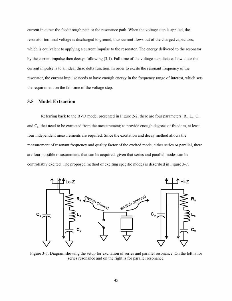
45
current in either the feedthrough path or the resonance path. When the voltage step is applied, the
resonator terminal voltage is discharged to ground, thus current flows out of the charged capacitors,
which is equivalent to applying a current impulse to the resonator. The energy delivered to the resonator
by the current impulse then decays following (3.1). Fall time of the voltage step dictates how close the
current impulse is to an ideal dirac delta function. In order to excite the resonant frequency of the
resonator, the current impulse needs to have enough energy in the frequency range of interest, which sets
the requirement on the fall time of the voltage step.
3.5 Model Extraction
Referring back to the BVD model presented in Figure 2-2, there are four parameters, Rs, Lx, Cx
and Co, that need to be extracted from the measurement; to provide enough degrees of freedom, at least
four independent measurements are required. Since the excitation and decay method allows the
measurement of resonant frequency and quality factor of the excited mode, either series or parallel, there
are four possible measurements that can be acquired, given that series and parallel modes can be
controllably excited. The proposed method of exciting specific modes is described in Figure 3-7.
Figure 3-7. Diagram showing the setup for excitation of series and parallel resonance. On the left is for series resonance and on the right is for parallel resonance.

46
The left of Figure 3-7 shows the excitation of series resonance by connecting the resonator to a
low impedance source. Since the impedance of the source is much lower than the impedance of Co near
the resonant frequency, current is forced to flow between the source and the resonance branch. In this
case, resonance involves only Rs, Lx and Cx, as in the series resonance behavior. The right of Figure 3-7
shows the excitation of the parallel resonance mode where the resonator is now connected to a high
impedance source that is much higher than the impedance of Co, thus forcing the current to flow between
Co and the resonance branch. In this case, resonance involves Rs, Lx, Cx and Co, as in the parallel
resonance behavior. Thus, by using an excitation and decay method with different source impedance, zero
or infinite, both series and parallel resonance can be deterministically excited allowing series resonant
frequency (fs), series quality factor (Qs), parallel resonant frequency (fp) and parallel quality factor (Qp) to
be measured. These parameters are analytically derived in (2.3), (2.4), (2.5) and (2.6). Once fs, Qs, fp, and
Qp are successfully measured, they can be used to extract model parameters Rs, Lx, Cx and Co.
However, one assumption in this formulation is that a source can be created that has low enough
impedance to truly excite the series resonance, which is not a realistic one. For high-frequency resonators,
the impedance of Co becomes quite small around the frequency of interest. For example 1 pF of Co at 1
GHz is equivalent to an impedance of around 160 Ω, which is comparable to the impedance of a
reasonably sized transistor switch available in advanced processes, an appropriate device to implement
the function of the source described above. If the source impedance is not low enough, part of the current
will flow though Co and the excited resonance is not the true series resonance, in which case, using the
analytical model for series resonance as in (2.3), (2.4) results in error in model parameter extraction. In
order to solve this, a different model for series resonance, shown in Figure 3-8, that includes the effect of
the nonzero impedance (Rsw) of the source when implemented using a transistor switch is used in model
extraction. The effect of the source impedance on fp and Qp is negligible because the impedance of the
switch in the off-state is much larger compared to the impedance of Co.

47
Figure 3-8. Resonator model including the switch resistance from the test circuit.
However, now with the effect of the source impedance included in the model, there are five
model parameters that need to be extracted but only four independent measurements, which do not
provide enough degrees of freedom for model parameter extraction. In order to resolve this issue, an
additional measurement, either Co or Rsw, is necessary. In the proposed method, both Co and Rsw are
measured to gain an extra degree of freedom, which allows increased accuracy of extraction in the
presence of measurement errors. As will be explained in Section 4.4.1, due to the novel excitation circuit,
other than the increased testing time, there is almost no cost in measuring both Co and Rsw compared to
measuring only one of them.

48
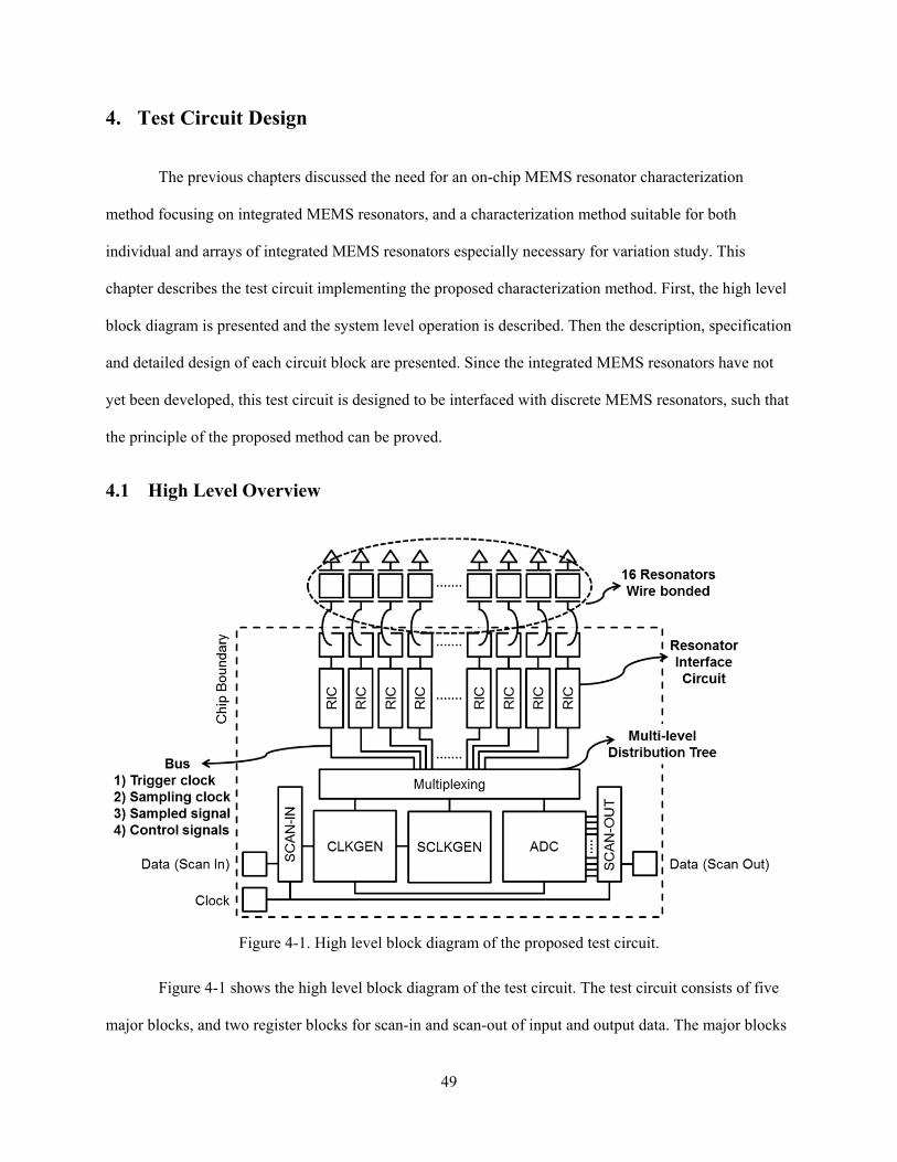
49
4. Test Circuit Design
The previous chapters discussed the need for an on-chip MEMS resonator characterization
method focusing on integrated MEMS resonators, and a characterization method suitable for both
individual and arrays of integrated MEMS resonators especially necessary for variation study. This
chapter describes the test circuit implementing the proposed characterization method. First, the high level
block diagram is presented and the system level operation is described. Then the description, specification
and detailed design of each circuit block are presented. Since the integrated MEMS resonators have not
yet been developed, this test circuit is designed to be interfaced with discrete MEMS resonators, such that
the principle of the proposed method can be proved.
4.1 High Level Overview
Figure 4-1. High level block diagram of the proposed test circuit.
Figure 4-1 shows the high level block diagram of the test circuit. The test circuit consists of five
major blocks, and two register blocks for scan-in and scan-out of input and output data. The major blocks

50
are Clock Generation (CG), Sampling Clock Generation (SCG), Resonator Interface Circuits (RICs),
Sampled Voltage Multiplexer (SVMUX) and Analog-to-Digital Converter (ADC). CG creates various
clocks necessary for the operation of the test circuit. SCG creates the sub-sampling clock that is used by
the RIC to sample the resonator terminal voltage. Each RIC interfaces with one resonator and it excites,
senses and samples the resonator response. These sampled voltages from RICs are connected to the ADC
through SVMUX. Finally, ADC converts the output of SVMUX into digital code, which is the final
output of this test circuit.
Figure 4-2. Clock waveforms showing the operation of the proposed test circuit.
Figure 4-2 shows important clock waveforms and system level operation of the test circuit. The
test circuit only requires one external clock (sysclk) that is running at around 10 MHz, and all other
clocks necessary for system operation are created on chip. There are three main clocks used in this test
circuit, trigger clock (tclk), sampling clock (sclk) and conversion clock (cclk), and they are generated
from sysclk. The rising edge of tclk is used to excite the resonator and it functions as a starting point of all
operation in the test circuit. The sclk is generated off of tclk with a programmable delay, and the rising
edge of sclk is used to sample the resonator terminal voltage. Lastly, the rising edge of cclk starts the
analog-to-digital conversion and the falling edge of cclk stops it. The output data is ready at the end of
each tclk period. Before each measurement cycle, the test circuit control bits are scanned in using sysclk
and after each measurement cycle, the output data is scanned out also using sysclk.

51
4.2 Clock Generation (CG)
Figure 4-3. Simplified circuit diagram of clock generation block.
The simplified circuit diagram of the Clock Generation block is shown in Figure 4-3. As shown
in the diagram, the CG block consists of an 8-bit counter that is running off of sysclk, four comparator
blocks, two edge generation blocks and two flip flops. The counter counts the rising edge of sysclk whose
output is compared to four 8-bit control signals tclkrcnt, tclkfcnt, cclkrcnt and cclkfcnt, which sets the
rising and falling edges of tclk and cclk. When the counter output is equal to the control bits, the edge
generation block sets the input of the flip flop to an appropriate state, which is clocked by sysclk to
produce tclk and cclk. In order to create differential clocks, sense amplifier based flip flops are used with
a cross-coupled inverter chain to buffer the clocks. By using this architecture, the location of the rising
and falling edges of tclk and cclk can be programmed from off-chip thus allowing control of the total
measurement time and conversion time, which are set by the pulse width of tclk and cclk respectively.
With the 10 MHz clock used for sysclk, the measurement time can be set as low as 400 ns and as high as
25.6 us, which is a wide range allowing this test circuit to accommodate various types of resonators with
different resonance frequency and quality factor. Table 4-1 summarizes required measurement time for
resonators with different resonance frequency and quality factor.
52
Series Resonance Frequency (fs) Series Quality Factor (Qs) Decay Time Constant (τ) 600 MHz 1000 0.53 us 600 MHz 2000 1.06 us
1 GHz 2000 0.63 us 2 GHz 2000 0.32 us
Table 4-1. Measurement time required for resonators with different series resonant frequency and quality factor.
4.3 Sampling Clock Generation (SCG)
Sampling clock (sclk) is the sub-sampling clock described in Section 3.4.1 whose frequency
needs to be slightly different from tclk for the sub-sampling technique to work. However, it is not a trivial
task to create or bring on-chip two different clocks whose offset frequency is precisely controlled. Also,
these clocks need to have low jitter for applications that require high effective sampling frequency, which
makes this task even more difficult. If the roles of the clocks are looked at more carefully, it becomes
clear that these two clocks with offset frequency actually provide two edges whose delay between them
increases every cycle. So, what is actually required in the sub-sampling technique is not necessarily two
clocks, but rather two edges, one that triggers and generates the input signal, and the other that samples
the input signal whose delay from the trigger edge is accurately controllable. Creating two edges with
controllable delay, though it does have its own challenges, is much easier to implement on-chip than
creating two clocks with small offset frequency. Looking at the operation with delayed edges in more
detail, in a given cycle, the rising edge of tclk triggers and generates the input signal, which is sampled by
the rising edge of sclk that is also generated from the tclk edge and delayed by td. In the following cycle,
the edge of tclk, again, generates the identical input signal and an edge of sclk, now delayed by td+∆t,
samples the signal.
While creating edges with controllable delay is easier than creating clocks with precise offset
frequency, it has to be designed carefully such that the delay is precisely controlled and the range of
generated delay is large enough to cover the desired length of the input signal. For example, if 1 us
window of signal needs to be sampled with effective sampling period of 1 ns, then the delayed edge of

53
sclk needs to span 0 to 1 us with 1 ns resolution, which is a challenging task. The easiest and most often
used method of producing delay on-chip is by utilizing the delay of logic gates such as inverters. In
advanced processes, fanout of 1 (FO1) delay can be as small as 10s of picoseconds. However, an inverter
delay has a strong dependency on process, voltage or temperature (PVT) variations, thus its value cannot
be estimated from simulation. For this reason, usually a feedback loop such as a delay-locked loop (DLL)
or a phase-locked loop (PLL) is used so that the delay is controlled using an ideal reference. In previous
works, a single delay locked loop (DLL) or a coupled DLL was used to generate the sampling edge,
achieving ∆t as small as sub-10 ps [30] [31]. Though it works well, designing DLLs is not a trivial task,
with many critical design issues such as jitter and stability as well as area overhead.
In this work, a new method is proposed that involves much simpler design yet is more robust
compared to the DLL solution. In the proposed method, the feedback loop is replaced by a ring oscillator
and a multi-phase counter that measures the average delay of a stage in the ring oscillator. The idea is that
rather than controlling the delay of an inverter so that it is a known value, let it be affected by PVT
variation but measure the delay off-chip and calculate the value. As long as the delay measurement is
accurate, the two methods should essentially achieve the same purpose. However, there are some
limitations to this method. First, the minimum delay cannot be controlled because, without the feedback
loop, the minimum delay is entirely set by PVT. So, there has to be enough margin on the minimum delay
such that even in the worst case variation, fine enough delay is produced for the required application.
Second, because there is no feedback loop to correct any phase noise that exists in the ring oscillator, jitter
accumulates as the number of cycles increases. So, an edge that is 1 us delayed has much larger jitter than
an edge that is 10 ns delayed. This fact needs to be carefully taken into account when calculating the jitter
specification of the ring oscillator. Lastly, because the delay measurement is done essentially by assuming
that the delay of each stage in the ring oscillator stays constant during the measurement, it has to be
verified that the variation in delay during the measurement, especially due to voltage and temperature
variation, causes negligible error in delay measurement.

54
A simplified circuit diagram of the proposed sampling clock generation is shown in Figure 4-4.
The block consists of a 16-stage ring oscillator with enable, two 16:1 MUX, a phase interpolator, an edge
selection circuit and a multi-phase counter. The operation of the SCG block is shown in Figure 4-5.
Figure 4-4. Simplified circuit diagram of sampling clock generation (SCG) block.
Figure 4-5. Clock waveforms showing the operation of sampling clock generation and principle of edge selection.
The rising edge of tclk enables the oscillator and it starts producing 16 clocks (32 clocks
including complementary). Out of 16 clocks, two are chosen with two 16:1 MUXs and they are fed into
the phase interpolator, which outputs a single clock. Finally, this clock is fed into the edge selection
circuit, which uses a counter output to select a desired edge. Output of the edge select circuit is the
sampling clock that is distributed to the RICs. So, by selecting different clocks from the oscillator and
doing phase interpolation, delay resolution of approximately FO1/2 can be achieved, where FO1 is the

55
delay of a single stage in the ring oscillator. The details of each circuit block are described in the
following sections.
4.3.1 Ring Oscillator
A 16-stage inverter-based pseudo-differential feed-forward ring oscillator with enable is used in the SCG
block, as shown in Figure 4-6. At the top is the oscillator level showing the detailed connection between
each stage in the ring. Additional to the typical connection between the adjacent stages, there are feed-
forward connections made between every other stage. In a traditional inverter-based pseudo-differential
ring oscillator, the cross-coupling connection is made between the outputs of the same stage, forcing the
two rings to be 180 degrees out of phase with each other. However, in a feed-forward architecture,
outputs of a stage are feed-forwarded two stages ahead causing the output of that stage to transition earlier,
thereby decreasing the rise and fall time of each stage and increasing the oscillator frequency. This feed-
forward technique has been demonstrated previously [32] [33] [34] and is used to increase the oscillation
frequency without reducing the number of stages in the ring. The circuit diagram of an individual stage is
shown at the bottom of Figure 4-6. Two large tri-state inverters, I0 and I1, are the main inverters that
make up the ring, and two medium tri-state inverters, I2 and I3, are the feed-forward cross-coupling tri-
state inverters. The cross-coupling inverters are sized one-fourth of the main inverters, to ensure
writability. The tri-state inverters, I4 and I5, are used to initialize the stage to a known state. This is
necessary to ensure deterministic start up once the oscillator is enabled. Figure 4-7 shows the state of the
ring when the oscillator is disabled. Once the oscillator is enabled, clk<0> always switches from 0 to 1,
which is required for edge selection to work correctly.

56
Figure 4-6. Simplified circuit diagram of 16-stage inverter-based pseudo-differential ring oscillator with enable for sampling clock generation. Circuit diagram of an individual stage (bottom).
Figure 4-7. Simplified circuit diagram showing the state of the oscillator when disabled with value of enabling signals.
As mentioned in Section 3.4.1, one critical requirement of the sampling clock is that clock jitter
needs to meet the specification for the effective sampling frequency, which can be as high as 10 GHz. In
this application, because the sampling is done on a signal with known form, which is a sinusoid with
decaying envelope, the jitter requirement is much relaxed compared to the general sampling case. The
devices are sized appropriately to achieve the required jitter specification.

57
4.3.2 16:1 MUX
The MUX used in this block is a pseudo-differential 16:1 MUX that consists of five identical
pseudo-differential 4:1 MUXs. The circuit diagram of a 4:1 MUX is shown in Figure 4-8. Tri-state
inverters are used to select the input, and the cross-coupled output stage is used to buffer and improve
duty cycle of the output clocks.
Figure 4-8. Simplified circuit diagram of pseudo-differential 4:1 MUX.
4.3.3 Phase Interpolator
A phase interpolator is used to create finer resolution in the delay. It takes two clocks and
produces a clock whose edges are the midway between the edges of the two input clocks. Since
interpolation is always done evenly, a simple inverter-based interpolator is used in this design. The circuit
diagram and operation is shown in Figure 4-9.

58
Figure 4-9. Simplified circuit diagram of phase interpolator and clock waveforms showing the principle of operation.
4.3.4 Edge Select Circuit
The edge select circuit is shown in Figure 4-10. The output clock of the phase interpolator circuit
clocks the counter whose output is compared with the 8-bit control signal sclkcnt. If they are equal an
edge is produced, which is the final sampling clock distributed to RICs.
Figure 4-10. Simplified circuit diagram of edge selection circuit
4.4 Resonator Interface Circuit (RIC)
Each resonator is connected to one resonator interface circuit (RIC) that excites, senses and
samples the resonator response. The RIC consists of an excitation circuit and a sensing circuit. The main
role of the excitation circuit is to excite the resonator in series and parallel resonant modes and to carry
out necessary additional measurements as described in Section 3.5. The sensing circuit consists of signal
buffers and a sampling head (SH) that is used to sample the resonator response. The high level block
diagram of the RIC is shown in Figure 4-11. The following sections describe the operation and detailed
design issues with each block.

59
Figure 4-11. High level block diagram of resonator interface circuit.
4.4.1 Excitation Circuit
Figure 4-12. Simplified circuit diagram of excitation circuit.
The excitation circuit consists of two PMOS devices, two NMOS devices and a transmission gate
as shown in Figure 4-12. P0 and P1 are pull-up devices and N0 and N1 are pull-down devices. P1 in all
RICs are tied together at their sources and are connected to a pad, which will be connected to a DC test
current (Itest) source. This device is used for switch resistance and capacitance measurement, which will
be described in detail in the following section. Finally the transmission gate is used to pass a DC
calibration voltage supplied from an off-chip digital-to-analog converter (DAC) for signal path calibration.
The excitation circuit has five operating modes: series resonance measurement, parallel resonance
measurement, switch resistance measurement, capacitance measurement and calibration. When a
particular RIC is not used, it is disabled such that it does not affect the operation of the enabled RIC. One
of the key design criteria for the RIC is that the undesired effects of the devices associated with the test
circuit are minimized such that the characteristic of the device under test is accurately captured. For this
reason, reducing the number of devices connected to the resonator terminal was a key goal in designing

60
the excitation circuit. A novel excitation structure is proposed which consists of six transistors carrying
out all required excitations and measurements for accurate model parameter extraction.
4.4.1.1 Series Resonance Measurement
Figure 4-13. Excitation circuit operation in series resonance measurement mode.
During series resonance measurement mode, the resonator is excited into series resonance to
measure the series resonant frequency and series quality factor. The operation is described in Figure 4-13.
In this mode, only P0 and N0 are used, while P1 and N1 are turned off. Notice that the source of N0 is
connected to VGX, which is a quiet low impedance DC voltage explicitly used for resonator excitation.
This voltage is used so that the DC bias of resonator response can be set from a quiet off-chip source.
Before measurement starts, the resonator terminal is initialized to VDD with P0 pulling it up.
Measurement starts at the rising edge of tclk as it turns off P0 and turns on N0 to discharge the resonator
terminal to VGX, thus applying a current impulse. In order to excite the series resonance of the resonator,
there needs to be enough energy around the frequency range of interest. To ensure this, N0 needs to be
sized appropriately to satisfy the resonator terminal node fall time requirement. Once the resonator is
excited, N0 stays on, providing a low impedance path to VGX. As mentioned in Section 3.5, because of
the finite resistance of N0, true series resonance cannot be excited, which is why the resistance of N0
needs to be measured so that the effect of this resistance can be removed in post-processing. Once the

61
measurement is done, the circuit returns to the initial state with P0 on and N0 off pulling the resonator
terminal to VDD.
4.4.1.2 Parallel Resonance Measurement
Figure 4-14. Excitation circuit operation in parallel resonance measurement mode.
During parallel resonance measurement mode, the resonator is excited into parallel resonance to
measure the parallel resonant frequency and parallel quality factor. The operation is described in Figure
4-14. The operation is identical to the series resonance measurement mode right up to the excitation of the
resonator with the current impulse. In series resonance measurement mode, N0 stays on to provide low
impedance path to VGX; however, in parallel resonance measurement mode, N0 turns off a set amount of
time after turning on. So, after N0 turns off, seen from the resonator terminal, the excitation circuit is high
impedance. This forces the resonator current to go through the feedthrough capacitance, thus exciting
parallel resonance. Since the switch resistance in off state is much higher than the impedance of the
feedthrough capacitance, the excited resonance is the actual parallel resonance. Notice from Figure 4-14
that because the other resonator terminal is connected to ground, any parasitic capacitance due to the
excitation circuit, bond pad and resonator contact capacitances all add on to the true device feedthrough
capacitance of the resonator. Thus, the effective feedthrough capacitance, once the resonator is attached to
the circuit, is indeed different from the design value and is unknown. Since parallel resonant frequency

62
and parallel quality factor are functions of this capacitance, knowing this value provides an extra degree
of freedom for model parameter extraction as described previously in section 3.5. Measurement of this
feedthrough capacitance is described in the Section 4.4.1.4. As in series resonance measurement mode,
once the measurement is done, the circuit returns to the initial state by pulling the resonator terminal to
VDD.
4.4.1.3 Switch Resistance Measurement
Figure 4-15. Excitation circuit operation in switch resistance measurement mode.
As mentioned in Section 4.4.1.1, the switch resistance of N0 needs to be measured in order to
allow correct model extraction. Figure 4-15 shows the operation of the switch resistance measurement
mode. In this mode, only P1 and N0 are used while P0 and N1 are turned off. Initially, P1 is off and N0 is
on, pulling the resonator terminal down to VGX. When measurement starts with the rising edge of tclk,
P1 turns on and N0 stays on, allowing DC current to flow through N0. Due to the resistance of N0, there
is an IR drop across N0, which shows up at the resonator terminal as additional voltage above VGX.
However, because of the IR drop that also exists on VGX due to the finite resistance of the VGX grid,
both on-chip and on-board as well as any amount of offset that exists in setting VGX, its exact voltage is
unknown and cannot be assumed as what is set off-chip. In order to solve this issue, two separate
measurements, with different amount of DC current are necessary. This way, the difference in voltage can

63
be used to calculate the resistance of N0. Though the VGX IR drop also is a function of DC current, since
it is much less than the switch resistance, it can be assumed constant.
4.4.1.4 Feedthrough Capacitance Measurement
Figure 4-16. Excitation circuit operation in feedthrough capacitance measurement mode.
As mentioned in Section 4.4.1.2, due to parasitic capacitance on the resonator terminal, the exact
feedthrough capacitance is unknown. In order to measure this value, a similar method is used as in the
switch resistance measurement, as shown in Figure 4-16. In this mode, only P2 and N2 are used with P1
and N1 turned off. Initially, N2 is on pulling the resonator terminal to ground. When measurement starts
with the rising edge of tclk, P2 turns on and N2 turns off, thereby charging the feedthrough capacitance
with DC current. Capacitance can be calculated from the slope of this charge-up curve. One thing to note
is that because the parasitic capacitances hanging off of the resonator terminal from transistors are
nonlinear, to get an accurate measurement of capacitance associated with parallel resonance, capacitance
extraction needs to be done from the charge-up curve around VGX.

64
4.4.1.5 Calibration
Calibration is critical for this test circuit because the ADC must be calibrated and the effects of
measurement related circuits need to be removed. Calibration is simply done by applying known DC
voltages to the resonator terminal through a transmission gate as shown in Figure 4-12. While calibrating,
P0, P1, N0 and N1 are all turned off. The calibration voltage goes through the sensing circuit and is
applied to the ADC input, thus the entire signal path from the resonator terminal to ADC is characterized
and later taken out in the post-processing step.
4.4.1.6 Disabled
Figure 4-17. Excitation circuit operation in disabled mode.
When the particular resonator is not being characterized, the RIC attached to that resonator is in
disabled mode. In this case, the resonator terminal is pulled down to ground through N1, as shown in
Figure 4-17, to avoid the resonator terminal floating and affecting characterization of other resonators.
4.4.2 Sensing Circuit
The sensing circuit consists of a buffer for resonator response processing, a sampling head (SH)
for sub-sampling and a sampled-voltage buffer as shown in Figure 4-18. The resonator terminal voltage is
first buffered and then sampled by the SH, which operates on sclk domain. The sampled voltage is then
buffered by the sampled-voltage buffer, which can drive the output load and the ADC. Multiplexing
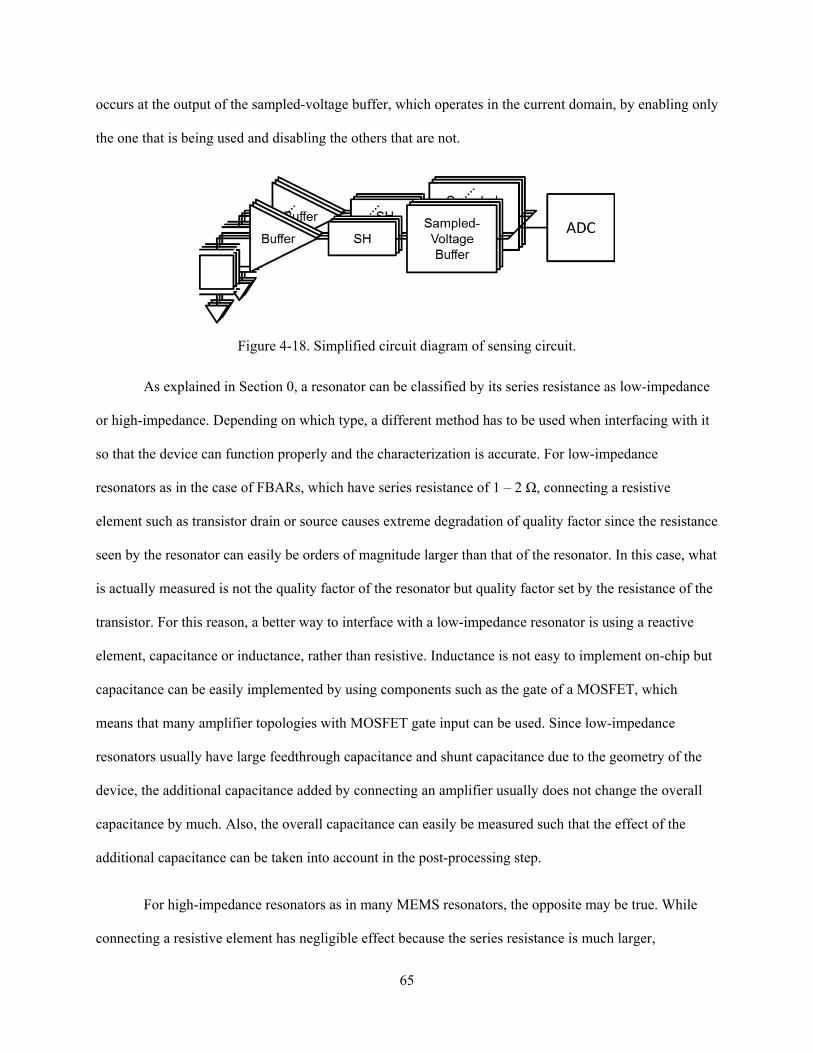
65
occurs at the output of the sampled-voltage buffer, which operates in the current domain, by enabling only
the one that is being used and disabling the others that are not.
Figure 4-18. Simplified circuit diagram of sensing circuit.
As explained in Section 0, a resonator can be classified by its series resistance as low-impedance
or high-impedance. Depending on which type, a different method has to be used when interfacing with it
so that the device can function properly and the characterization is accurate. For low-impedance
resonators as in the case of FBARs, which have series resistance of 1 – 2 Ω, connecting a resistive
element such as transistor drain or source causes extreme degradation of quality factor since the resistance
seen by the resonator can easily be orders of magnitude larger than that of the resonator. In this case, what
is actually measured is not the quality factor of the resonator but quality factor set by the resistance of the
transistor. For this reason, a better way to interface with a low-impedance resonator is using a reactive
element, capacitance or inductance, rather than resistive. Inductance is not easy to implement on-chip but
capacitance can be easily implemented by using components such as the gate of a MOSFET, which
means that many amplifier topologies with MOSFET gate input can be used. Since low-impedance
resonators usually have large feedthrough capacitance and shunt capacitance due to the geometry of the
device, the additional capacitance added by connecting an amplifier usually does not change the overall
capacitance by much. Also, the overall capacitance can easily be measured such that the effect of the
additional capacitance can be taken into account in the post-processing step.
For high-impedance resonators as in many MEMS resonators, the opposite may be true. While
connecting a resistive element has negligible effect because the series resistance is much larger,

66
connecting a capacitive element can cause even functional failure as described in Section 2.2.3. Thus, in
deciding the method for interfacing with a resonator, the impedance of the resonator is a critical factor
that must be taken into account.
4.4.2.1 Resonator Terminal Voltage Buffer Design
The resonator terminal voltage buffer consists of a source-follower input stage and two cascaded
stages of a self-biased resistive-peaked common-source-based amplifier as shown in Figure 4-19. A
source-follower stage was used at the input in order to avoid introducing a low-impedance path to the
resonator terminal. Topologies such as common-source have large Miller capacitance from the input to
the output, which can provide low enough impedance path to transistor output resistance. This additional
path causes energy in the resonator to dissipate, therefore degrading the quality factor. However, because
the source-follower has positive gain, it has a negligible amount of capacitance between the input and the
output. To improve linearity, the body of PB0 is tied to the source rather than VDD.
The two additional stages are necessary to drive the SH at the output of this buffer. The first and
second stages use the same topologies, except the second stage has larger sizing for driving the output
load. This topology is based on a common-source amplifier with NMOS input and PMOS diode
connected load. The only difference is that the diode connection is made with a transmission gate, which
acts as a resistive element. The advantage of the diode connected load is that there is no need to generate
a bias voltage for the PMOS load. However, because the diode connected load is low-impedance seen
from the output, the stage suffers from low gain. On the other hand, having a biased PMOS load offers
large gain, but a separate bias voltage needs to be generated, and having large gain causes difficulty in
cascading stages because the output DC level of the first stage can have wide range and can easily put the
second stage a in low-gain operating region. The goal of the proposed topology is to combine the
advantages of diode connected load and biased load so that the amplifier can be self-biased yet have large
gain when it is desired.

67
The proposed topology can be easily analyzed in the following way. The RC filter formed by the
transmission gate and the capacitance at the gate of the PMOS acts as a short for low-frequency but an
open for high-frequency. In DC and low-frequency range, the gate of the PMOS tracks the output node,
thus acting as a regular diode-connected load, and offers the desired self-biasing. In high-frequency range,
above the pole caused by the RC filter, the gate of the PMOS no longer tracks the output node, thus acting
as a biased load and achieving the desired large gain. Also, because the transmission gate shields the large
gate capacitance of PMOS from the output node, bandwidth is enhanced compared to the regular diode
connected load common-source amplifier. This is a similar technique as inductive peaking where an
inductor is used to shield a capacitance thus enhancing the bandwidth of the amplifier.
Figure 4-19. Simplified circuit diagram of resonator terminal voltage buffer.
4.4.2.2 Sampling Head (SH) Design
The sampling head (SH) is a critical circuit that needs to sample the high-frequency resonator
response for sub-sampling. Along with the buffer described in the previous section, these two circuits
handle the highest frequency on-chip, so additional care in design is needed. SHs are typically used for
on-chip measurement or on-chip oscilloscope applications and different types of SHs have been designed
in the past. [28] [29] [30] [35] [36] [37]. The advantage of the SH is that it can be designed to be small
costing negligible area and, most importantly, thus introduce insignificant amount of parasitic resistance

68
and capacitance to the critical signal being observed. There are a number of different topologies each with
advantages and disadvantages, but a two-stage design is used in this work as in [37].
Figure 4-20. Simplified circuit diagram of sampling head circuit and current-mode buffer.
As shown in Figure 4-20, the first stage is a simple transmission gate formed by P0 and N0 and a
hold capacitor C0. In sample and hold designs, often only an NMOS switch is used with clock
bootstrapping to allow rail-to-rail input voltage and also to minimize nonlinearity caused by input
dependent gate overdrive. However, a clock bootstrapping circuit requires a bootstrap capacitor, which
consumes non-negligible amount of area. So in this design, instead of an NMOS switch, a CMOS
transmission gate is used to reduce size overhead and allow rail-to-rail input voltage, but at the cost of
some nonlinearity. However, as will be explained later, this input dependent nonlinearity is deterministic,
so it can be canceled by calibration. Since, the first stage has to process a high-frequency signal, the
CMOS transmission gate and hold capacitor are sized such that the bandwidth of the stage is around 4
GHz, which well exceeds the highest frequency that has to be processed.
The second stage consists of two transmission gates, formed by P1, N1, P2 and N2, and a hold
capacitor C1. The transmission gate formed by P1 and N1 is used to redistribute charges between two

69
hold capacitors C0 and C1, while the transmission gate formed by P2 and N2 is used to initialize voltage
on C1 before sampling. The final voltage on C1 after sampling and redistributing is given by (4.1).
0 11
(4.1)
Since charges are redistributed, there is a gain of less than one from the first stage to the second stage, but
using this technique ensures that the final voltage is always referenced to the initialized voltage on C1.
This eases the design of the following stage by limiting the input voltage range. In case more gain is
needed, a simple opamp based amplifier with relaxed bandwidth requirement can be used because the
sampled voltage is now at much lower frequency than the original signal. Thus, by changing the location
of the amplifier in the signal path, the design requirement can be relaxed significantly.
One of the key design considerations, as in most sampling circuits, is the leakage from the hold
capacitor, especially if sampling frequency is low as it is in sub-sampling.
,
/ 1 / 1 (4.2)
As shown in (4.2), since leakage current is sampled voltage dependent, theoretically, it should be
possible to calibrate it out. However, because sub-threshold leakage current, which is the dominant
component of leakage current in this case, is also a strong function of temperature (exponential), unless
calibration is done in a temperature controlled environment, it cannot be eliminated by calibration.
Unfortunately, there are really only two ways to tackle this issue. The first way is to reduce the actual
leakage current by using different device type or by adjusting transistor terminal voltages. The most
effective way is to use a high threshold voltage (Vt) device, if available, since Vt has exponential effect
on leakage current. There are also other techniques such as using negative gate overdrive voltage, which
also has an exponential effect, raising the Vt by reverse biasing the body terminal and reducing drain to
source voltage by appropriately biasing the drain or the source node. However, usually voltage solutions
are costly because of difficulty in bringing a quiet voltage on-chip.

70
The second way is to increase the hold capacitance so that the effect of leakage current on the
sampled voltage is reduced. For example, with 10 times larger hold capacitance with same amount of
leakage current, the change in sampled voltage during a set amount of time is 10 times less. However, the
drawback of this approach is that, in the single-stage case, the bandwidth of the circuit is reduced by 10
times and, in the two-stage case, the gain from first to second stage is reduced by 10 times if the first-
stage bandwidth is kept the same. The gain degradation may be easily fixed by using an amplifier after
the SH as mentioned previously, but noise on the hold capacitors ultimately limits the minimum allowed
voltage. Thus, noise on hold capacitors, mostly dominated by kT/C noise, must be analyzed carefully
before setting the size of hold capacitors and gain between the first and second stage.
In this design, the first-stage is designed with regular-Vt devices to achieve maximum bandwidth,
and all second-stage transistors are high-Vt devices to minimize leakage current. C0 and C1 are formed
by transistor parasitic capacitance, rather than metal or MOS capacitors. This is possible in this case
because the gain is set by the ratio of C0 and C1, not by their absolute values. Also, the nonlinearity of
parasitic capacitance does not cause any issues, because both C0 and C1 behave in the same way, at least
to first order, and more importantly this effect can be calibrated out.
The final sampled voltage is output using a current mode buffer as shown in Figure 4-20. It is
implemented as a simple current mirror as in [29] because of its convenience in doing multiplexing,
which will be discussed in the next section.
4.5 Sampled Voltage Multiplexing (SVMUX)
Multiplexing capability is one of the most important features required for on-chip characterization
structures. Ability to share as many common testing circuits as possible is critical, especially for reducing
area overhead and minimizing test circuit induced measurement errors. As mentioned in the previous
section, the output buffer for SH uses a current mode, so the multiplexing structure is done simply by
enabling and disabling the current mirrors as shown in Figure 4-21. In the case where more buffering is

71
necessary or more than one stage of multiplexing is necessary, similar current mirror structures with
different sizing can be used.
Figure 4-21. Simplified circuit diagram of sampled voltage multiplexing using current-mode buffer.
4.6 Analog-to-Digital converter (ADC)
The multiplexed SH voltage is converted to a digital code using an on-chip analog-to-digital
converter (ADC). There are a number of reasons for doing ADC on-chip rather than sending the analog
voltage off-chip and measuring it using an oscilloscope. Unlike the high-frequency resonator terminal
voltage, which is very challenging to send off-chip, the sampled voltage is at much lower frequency and
can be buffered to and probed from off-chip relatively easily. Also, nonlinearity, which was a concern in
sending high-frequency signals off-chip is no longer an issue since it can be easily calibrated out.
However, one reason for having ADC on-chip is so that the data interface is completely digital, which
makes testing automation much easier and efficient. Also, in order to drive the pad and the probe
capacitance, buffering is necessary, with which more noise is added to the signal. In this test circuit, both
options have been implemented for testing purposes such that the sampled voltage can either be converted
or directly probed from off chip. The ADC design used in this circuit is a voltage-controlled oscillator
(VCO) based one similar to designs previously demonstrated in [38] [39] [40] [41] [42].

72
4.6.1 Principle
A VCO-based ADC has been demonstrated in a number of applications including an on-chip
oscilloscope application [39] and as a quantizer in a ΣΔ modulator [42]. There are a number of key
advantages of using a VCO-based ADC over other architectures. First, as process and voltage scales, it
becomes more difficult to design the high-performance analog blocks required in traditional high-
performance architectures such as pipelined or flash architectures. Even though voltage-domain design is
becoming more difficult, time-resolution has been improving due to faster transistors, which allows for
new architecture such as a VCO-based one that utilizes time-domain designs [41].
The operating principle of the VCO-based ADC is shown in Figure 4-22. The sampled voltage
(Vs) acts as the control voltage for the oscillator, so the frequency of the oscillator depends on the
sampled voltage level. The output clock produced by the VCO clocks a counter for a set amount of time,
whose output represents the frequency of the clock. This counter output is the output digital code. The
output code can be expressed as (4.3) where TC is the conversion time and KVCO is the gain of the VCO.
In typical VCO design, VCO response is nonlinear and KVCO depends on the control voltage. Then the
conversion resolution, which depends on TC and KVCO is expressed as (4.4).
(4.3)
1
(4.4)
Figure 4-22. Diagram showing the operating principle of VCO-based ADC.

73
Due to the input dependency of KVCO, resolution is also input dependent. In applications such as this test
circuit, where the range of input voltage is relatively small, resolution can be assumed nearly constant.
As in all ADCs, improving resolution is almost always a desired goal. Two obvious methods can
be deduced by observing (4.4). One is to increase TC and the other is to increase KVCO. Increasing TC
allows the counter to count VCO clock edges for a longer amount of time, which makes it possible to
detect a smaller change in frequency, and thus sense smaller changes in Vs. However, there is an obvious
sampling frequency requirement that sets the largest allowable TC, but, not only that, this method is
ultimately limited by VCO clock jitter that accumulates as TC increases. There is a maximum TC, TC,max,
up to which point resolution increases with increasing TC, but beyond this, there is no improvement in
resolution. Increasing KVCO also improves the resolution because with larger KVCO, the same change in
voltage is translated to a larger change in VCO frequency, thus a smaller change in voltage can be
detected by the counter. To achieve maximum resolution, KVCO should be maximized through choosing
the optimum VCO architecture and design. However, there is a limit to how large KVCO can be and this
depends on the intrinsic device properties of a particular technology, such as transistor transconductance,
output resistance and parasitic capacitance.
It is not apparent from (4.4), but there is actually another easy way to improve the resolution.
Equation (4.4) expresses the number of clock rise edges that occur during time TC, which is accomplished
by the counter. The floor operation exists because the counter is inherently an integral operation. This
means that the smallest time unit in the conversion operation is the clock period. Any change in frequency
that translates to change in time less than a clock period over the conversion time cannot be detected by
the counter. Thus, decreasing the detectable time unit directly improves the resolution. This can be seen
by rewriting (4.4) as (4.5) where n denotes the factor by which the time unit is increased.
1
(4.5)

74
This can be easily done by noticing that there are often multiple phases in the VCO and using a different
counter architecture that can use multiple phases [39]. The detailed VCO and counter architecture and
design is discussed in the following sections.
4.6.2 Voltage-Controlled Oscillator Design
The VCO consists of a voltage-to-current circuit (V2I), a current-to-current circuit (I2I), a ring
oscillator (RO) and 16 level-shifters (LSs). The high-level architecture is shown in Figure 4-23.
Figure 4-23. High level block diagram of VCO architecture.
V2I and I2I are used to convert the control voltage to RO current. Change in control voltage is translated
to change in RO current, which in turn controls the frequency of the oscillation. A ring oscillator (RO) is
used in this design because of its high KVCO, robustness and ease of design. A 16-stage current-starved-
inverter-based pseudo-differential topology is used, which produces 16 pairs of differential clocks. The
clocks produced by the RO are less than full-swing because they are current starved, so they are level-
shifted to rail-to-rail swing using 16 differential LSs.
V2I and I2I are based on a current mirror topology as shown in Figure 4-23. The V2I consists of
NMOS transconductance devices and NMOS switches for programmability. NMOS devices whose gates
are connected to the control voltage produce current, which is mirrored using PMOS cascoded current
mirrors in I2I.

75
Figure 4-24. Simplified circuit diagram of V2I and I2I.
V2I is NMOS based because the control voltage, which is the sampled voltage, is referenced to
ground, thus using NMOS decreases the effect of ground supply noise. The programmability is
implemented in order to control KVCO of the VCO. By controlling the number of on devices in V2I,
transconductance of V2I and thus KVCO of the VCO can be controlled. I2I is designed using a cascoded
PMOS current mirror in order to improve power supply rejection ratio (PSRR). Power supply noise can
easily degrade the phase noise performance of VCO and thus jitter performance, which limits the
resolution in VCO-base ADC. In order to further improve PSRR, the VCO uses its own dedicated power
supply (VDDRO), with default value of 2.5V.
The 16-stage RO circuit is shown on Figure 4-25. Each stage is formed by four current starved
inverters, two large ones making up the actual rings and two small ones for cross-coupling the two rings.
The cross-coupling inverters are sized ¼ of the ring inverters to ensure writability. 16 stages are chosen to
reduce the oscillation frequency thus relaxing the counter operating frequency and at the same time
providing a reasonable number of bits for the encoder in the multi-phase counter.

76
Figure 4-25. . Simplified circuit diagram of 16-stage inverter-based pseudo-differential ring oscillator in ADC. Circuit diagram of an individual stage (bottom).
One of the most critical specifications is the phase noise performance because of the effect of
jitter on resolution. For a given process technology, there are limited ways to reduce phase noise for an
inverter-based RO, and the most effective way is to increase power consumption at a given oscillation
frequency. Though the phase noise analysis of RO is not straightforward because of its large signal
behavior with cyclostationary nature of noise, the concept can be illustrated by the fact that thermal noise
current (In) in the transistor increases as the square root of its width (or W/L), while the output impedance
decreases linearly with its width. Thus the output noise voltage (Vn) decreases as the square root of its
width. Because of the square root relationship, it can be observed that phase noise and jitter is reduced as
the square root of total current consumption of the oscillator, with diminishing return as devices become
very large.
4.6.3 Multi-phase Counter
Figure 4-26 shows the different phases of the VCO clocks. With the 16-stage pseudo-differential
RO, there are 32 phases that are evenly spaced out within one oscillation period. The idea of the multi-
phase counter is to observe the state of every phase of the RO to improve the resolution of the ADC, as
mentioned previously. There have been a number of different implementations achieving this function [38]
[39] and in this test circuit, a counter and registers are used to count the rising edge of a phase and capture
the state of every phase at the end of conversion as in [38]. This is illustrated in Figure 4-27.

77
Figure 4-26. Clock waveforms of different VCO clock phases showing states of the ring oscillator.
Figure 4-27. Simplified circuit diagram of multi-phase counter in ADC.
Once the chip powers up, the VCO in the ADC never turns off in order to prevent supply voltage
fluctuation during turning on and turning off. So, when conversion starts, there is no way to guarantee or
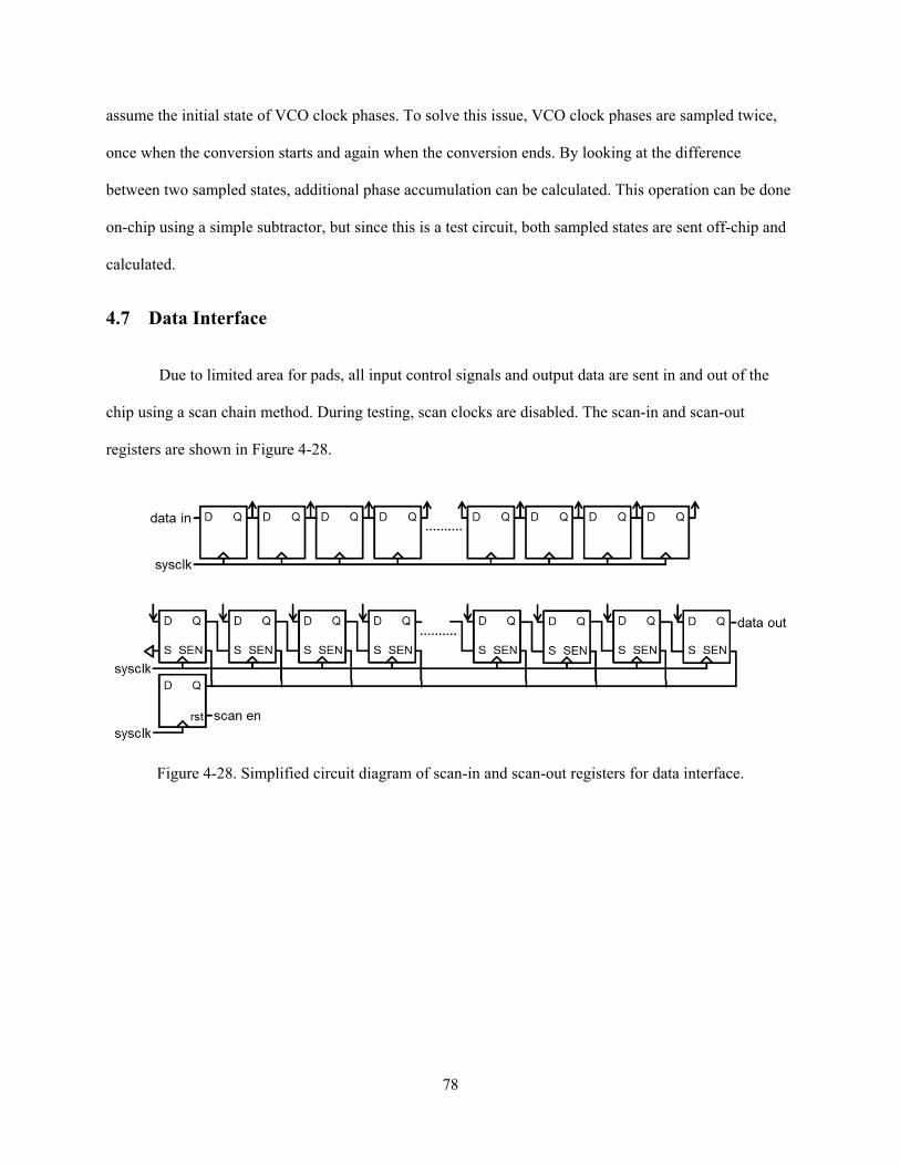
78
assume the initial state of VCO clock phases. To solve this issue, VCO clock phases are sampled twice,
once when the conversion starts and again when the conversion ends. By looking at the difference
between two sampled states, additional phase accumulation can be calculated. This operation can be done
on-chip using a simple subtractor, but since this is a test circuit, both sampled states are sent off-chip and
calculated.
4.7 Data Interface
Due to limited area for pads, all input control signals and output data are sent in and out of the
chip using a scan chain method. During testing, scan clocks are disabled. The scan-in and scan-out
registers are shown in Figure 4-28.
Figure 4-28. Simplified circuit diagram of scan-in and scan-out registers for data interface.

79
5. Post-Processing
The raw measurement data from the chip needs to be post-processed to do model extraction as
outlined in Section 3.5. However, before the measurement data can be used, the test circuit needs to be
calibrated in order to remove the effect of signal path on the measurement, which is critical for accurate
characterization. The test circuit is specifically designed such that calibration can be done easily and
accurately, the details of which are described in Section 5.1. In Sections 5.2 and 5.3, measurement
parameter and model parameter extraction steps are described in detail.
5.1 Calibration
Calibration is an absolutely necessary step for this test circuit for a number of reasons. First of all,
the ADC has to be calibrated because of nonlinear response of the VCO frequency to input voltage.
Before using the ADC, calibration must be done to produce a look up table (LUT) between input voltage
and output code, which is then used to translate the output codes into input voltage series using
interpolation. Also, because the VCO is sensitive to temperature variation, calibration has to be redone
from time to time if there is a change of temperature. Second, any nonlinearity in the resonator terminal
voltage buffer, the sampling head and sampled voltage multiplexer all add distortion to the resonator
decay signal. Since the accurate capture of the exponential decay envelope is required for accurate
characterization of the resonator quality factor, distortion will directly affect the accuracy of the
characterization. Also, the signal path is different between every resonator despite careful layout
matching. This difference affects the characterization, possibly exacerbating or shadowing the resonator
variation analysis. By calibrating each path separately, the effect of the signal path is completely taken out.
Figure 5-1 shows the calibration of a resonator signal path and ADC. A DC voltage fed in from
an off-chip DAC is used in calibration. As mentioned in Section 4.4.1.5, this calibration voltage drives the
resonator terminal node through a transmission gate in the excitation circuit. So the calibration is done on
the actual signal path as seen by the resonator terminal, which improves the accuracy of the calibration

80
result as well as measurement. Once the resonator terminal voltage is set, the test circuit operates as it
would in normal operation and outputs a code, which corresponds to the DC voltage from the DAC. This
calibration voltage is swept and with the corresponding output codes, the LUT is created. This calibration
step is done for every resonator that is being measured. Once the actual resonator measurement is done,
the LUT is used to translate the output codes into resonator terminal voltages, which are used for
parameter extraction.
Figure 5-1. High level block diagram showing the calibration of signal path and ADC.
5.2 Parameter Extraction
Once the resonator terminal voltage signal is recovered, depending on which measurement is
done, the corresponding parameters need to be extracted. As described in Section 3.5, four different sets
of measurements are done for each resonator, namely, series resonance measurement, parallel resonance
measurement, switch resistance measurement and capacitance measurement. The following sections
describe how parameters are extracted for each measurement.

81
5.2.1 Series and Parallel Resonance Measurement
As described in Section 3.3.4, the measured resonator terminal voltage signal for either series or
parallel resonance measurement is a sinusoid signal with an exponential decay envelope, which can be
expressed as (3.1). The oscillation frequency, fosc, and the decay time constant, τ, can be expressed as (3.2)
and (3.3). Thus, by extracting fosc and τ from the signal, resonant frequency and quality factor of a given
mode can be calculated. As can be seen from (3.2) and (3.3), fosc and τ are not independent parameters but
functions of independent parameter fo and Q. Therefore, extraction of fo and Q is done rather than of fosc
and τ. With this relationship, (3.1) can be rewritten as in (5.1).
cos 2 1
14
(5.1)
The extraction is done in MATLAB using a least square fitting method. The parameter extraction
process is shown in Figure 5-2.
Figure 5-2. Diagram showing the resonance measurement parameter extraction process.
Before extraction starts, the voltage signal is normalized such that A in (5.1) is set to 1. The
extraction process consists of three fitting steps. In the first step, fo, Q and ϕ are fitted. Then in the second
step, using the result of the first step, ϕ is fitted again while holding the other parameters constant. In the
last step, Q is fitted again while holding the other parameters constant. The reason for fitting in this

82
repetitive manner is to increase the fitting accuracy of Q, which requires accurate fitting of ϕ. Once the
extraction is done, resonant frequency and quality factor of the given resonance mode is acquired.
5.2.2 Switch Resistance Measurement
Extraction for switch resistance measurement is fairly simple. As explained previously, switch
resistance measurement is done with two different DC test currents in order to reduce the effect of IR
drop on VGX. Then the resonator terminal voltages for the two measurements can be written as
(5.2)
(5.3)
Then switch resistance can be calculated by
(5.4)
5.2.3 Feedthrough Capacitance Measurement
Capacitance measurement involves charging up the capacitance with a DC test current. Thus the
expected signal on the resonator terminal is a linear ramp, which can be easily fit using a linear model.
However, because part of the capacitance involved is non-linear, the signal is not exactly a linear ramp.
Since the capacitance that needs to be extracted is the one involved with resonance, only the part of the
curve around VGX, which is the DC level at which resonance occurs, is used for extraction. This is
described in Figure 5-3.

83
Figure 5-3. Diagram showing the feedthrough capacitance measurement parameter extraction method.
5.3 Model Extraction
The parameters extracted from the four sets of measurements are used to extract the resonator
model. The resonator equivalent circuit model with the excitation circuit is shown in Figure 5-4.
Figure 5-4. Resonator model including the switch resistance from the test circuit in series and parallel resonance excitation.
From the measurement, six parameters are extracted, namely, fs, Qs, fp, Qp, Rsw and Co. As seen in Figure
5-4, there are five parameters, Rs, Lx, Cx, Co and Rsw that need to be extracted, where Co and Rsw have
been directly measured. As mentioned in Section 3.5, because of possible error associated in measuring
Qs, it is discarded in model extraction, but rather used only for verifying the extracted model. Therefore,

84
three measured parameters, fs, fp and Qp are used to calculate the model parameters, Rs, Lx and Cx.
However, because the expression for fs is not concise, the model parameters are calculated numerically
using an iterative approach. The extraction process is described in Figure 5-5.
Figure 5-5. Diagram showing the model parameter extraction process.
Once model extraction is done, all the parameters necessary to completely characterize of a
resonator using the BVD model are available. Rs, Lx and Cx completely characterize the series resonance
behavior, which in turn also allows characterization of parallel resonance behavior for any given Co.

85
6. Simulation
This chapter discusses simulation methods for verifying the proposed individual circuits and
overall on-chip resonator characterization method. There are a number of difficult challenges with
simulating circuits such as these, where both short and long time scales are involved. Resonator response
and analog signal processing circuits in the signal path are all operating in a time scale in the range of
picoseconds to nanoseconds, while the sub-sampling circuits are operating over microseconds or longer.
In cases like this, simulation either suffers from unacceptably long simulation time if time steps are set
small, or from unacceptably low accuracy if time steps are set large. In order to solve this issue, both
circuit level simulation and system level simulation are done together. Individual circuit simulation is
mostly done using Cadence Spectre, while system level simulation is done using a behavioral simulator
written in MATLAB, which incorporates Spectre simulation results in its model.
6.1 Block Level Simulation
The Cadence Spectre simulator is used to verify cell level and block level circuit functionality.
One of the more challenging checks is the jitter simulation of the ring oscillators (RO) in sampling clock
generation (SCG) and analog-to-digital converter (ADC). Since the jitter in these blocks critically affects
the performance of the system, additional care is necessary in designing and simulating these blocks. In
order to calculate the RMS phase jitter in RO, phase noise simulation is done using the Spectre RF
simulator, and the simulated phase noise is used to calculate the RMS phase jitter using MATLAB. RMS
phase jitter can be calculated from phase noise using the relationship shown in (6.1), where L(f) denotes
the phase noise spectrum.
12
2 (6.1)

86
6.2 System Level Behavioral Simulation
System level simulation is done using a behavioral simulator written in MATLAB. The
behavioral models are created such that they have almost one-to-one correspondence with the actual
circuit in terms of circuit hierarchy and system level operation. This allows chip operation as well as
calibration to be tested in the behavioral model just as it would be done on chip. To increase the accuracy
of the models and simulation, circuit level simulation results for critical blocks are imported into the
behavioral models. These blocks include the resonator terminal voltage buffer, the sampling head and
VCO in the ADC. Some of the critical simulations done in the behavior simulator are to test the accuracy
of the proposed calibration scheme and the effect of noise and jitter on parameter extraction accuracy.
Because it is difficult to analytically derive the effect of noise and jitter on parameter extraction accuracy,
behavioral simulation is extensively used to derive specifications for each block. The system level
behavioral simulator block diagram is shown in Figure 6-1.
Figure 6-1. High level block diagram of MATLB behavioral simulator.
6.3 Simulation Result
Behavioral simulation results are shown in this section. Figure 6-2, Figure 6-3 and Figure 6-4
shows the reconstructed resonator terminal voltage, sampling head output voltage and ADC output codes
for series resonance measurement, parallel resonance measurement and feedthrough capacitance

87
measurement, respectively. The output codes for each measurement are used for measurement parameter
extraction and model parameter extraction. The model parameter extraction error is summarized in Table
6-1.
Figure 6-2. Plot of reconstructed signals for series resonance measurement. Resonator terminal and sampling head output voltage (top) and ADC output code (bottom).

88
Figure 6-3. Plot of reconstructed signals for parallel resonance measurement. Resonator terminal and sampling head output voltage (top) and ADC output code (bottom).
Figure 6-4. Plot of reconstructed signals for feedthrough capacitance measurement. Resonator terminal and sampling head output voltage (top) and ADC output code (bottom).

89
Parameter Extraction Error Rs < 1% Lx < 0.1 % Cx < 0.1 % fs < 100 ppm Qs < 1 %
Table 6-1. Summary of model parameter extraction error from behavioral simulation.

90

91
7. Summary and Future Work
This final chapter first summarizes the work presented in this thesis. This is followed by a brief
discussion of current work being done in test chip development and testing, as well as suggestions for
future work to extend this project to characterization of truly integrated MEMS resonators.
7.1 Summary
A test circuit for MEMS resonator characterization has been developed that can accurately and
efficiently characterize a large array of integrated on-chip resonators. The proposed characterization
method can multiplex and measure resonant frequencies and quality factors, allowing the extraction of the
BVD model widely used to model resonators. Due to a generalized characterization method implemented
by the test circuit, a wide range of resonators with different resonant frequency and quality factor can be
accurately characterized. This test circuit features a novel excitation circuit that can carry out impulse
response and accommodate a sub-sampling technique, which solves many challenges that exist with high-
frequency characterization. The sampling clock necessary for sub-sampling is generated using a novel
DLL-less architecture consisting of an enabled ring oscillator and frequency measurement circuit, which
offers simplicity and robustness compared to the other designs previously proposed. Finally, the on-chip
VCO-based ADC converts the sampled voltage and outputs a digital code allowing complete digital
interface beneficial for test-automation.
7.2 Current and Future Work
Design work is currently in progress for chip tapeout, planned for fabrication with National
Semiconductor Corporation in summer of 2011 using a 180 nm CMOS process. Chip testing
methodology development is also being done concurrently. The test circuit will be demonstrated with
discrete FBARs provided by Avago Technologies, and bar resonators developed by Professor Dana
Weinstein at MIT, which will be wire-bonded to the chip.

92
An important future application of this test circuit is characterizing arrays of integrated MEMS
resonators, for which using the existing characterization method has many challenges. A possible
implementation is shown in Figure 7-1. This test circuit will allow characterization of a large array of
integrated MEMS resonators without requiring probe pads for each device, thus not only saving area, but
also reducing parasitic effects that can be so devastating to the advanced devices. With increasing effort
to develop integrated MEMS resonators, this test circuit will provide a practical way to characterize these
emerging devices, solving many challenges associated with the existing methods.
Figure 7-1. High level block diagram of on-chip test circuit interfaced with an array of integrated MEMS resonators.

93
Bibliography
[1] J. R. Vig, “Quartz crystal resonators and oscillators for frequency control and timing applications - a tutorial”, SLCET-TR-88-1 (rev. 8.5.3.6), Jan. 2007.
[2] C. S. Lam, “A review of the recent development of MEMS and crystal oscillators and their impacts on the frequency control products industry,” in Proceedings of the 2008 IEEE Ultrasonics Symposium, Beijing, China, pp. 694-704, Nov. 2-5, 2008.
[3] C. T.-C. Nguyen, “MEMS technology for timing and frequency control,” IEEE Transactions on Ultrasonics, Ferroelectrics, and Frequency Control, vol. 54, no. 2, pp. 251-270, Feb. 2007.
[4] G. K. Fedder, R. T. Howe, T.-J. K. Liu, and E. P. Quévy, “Technologies for cofabricating MEMS and electronics,” Proceedings of the IEEE, vol. 96, no. 2, pp. 306-322, Feb. 2008.
[5] R. Ruby and P. Merchant, “Micromachined thin film bulk acoustic resonators,” in Proceedings of the 1994 IEEE International Frequency Control Symposium, Boston, MA, p. 135, Jun. 1-3, 1994.
[6] W.-T. Hsu and M. Pai, “The new heart beat of electronics - silicon MEMS oscillators,” in Proceedings of the 2007 IEEE Electronics Components and Technology Conference, pp. 1895-1899, May. 29, 2007.
[7] M. Lutz, A. Patridge, P. Gupta, N. Bunchan, E. Klassen, J. McDonald, and K. Petersen, “MEMS oscillators for high volume commercial applications,” in Proceeding of the International Solid-State Sensors, Actuators and Microsystems Conference, pp. 49-52, Jun. 2007.
[8] T. H. Lee, The design of CMOS radio-frequency integrated circuits, 2nd ed. New York, NY, USA, Cambridge University Press, 1988.
[9] J. D. III Larson, P. D. Bradley, S. Wartenberg, and R. C. Ruby, “Modified Butterworth-Van Dyke circuit for FBAR resoantors and automated measurement systems,” in Proceeding of the IEEE Ultrasonics Symposium, pp. 863-868, Oct. 2000.
[10] A. Chandrakasan, F. Fox, and W. J. Bowhill, Design of high-performance microprocessor circuits., Wiley-IEEE Press, 2000.
[11] M. Orshansky, S. Nassif, and D. Boning, Design for manufacturability and statistical design a constructive approach. New York, NY, USA, Springer, 2008.
[12] J. Wang, L. Yang, S. Petrangelo, Z. Ren, and C. T.-C. Nguyen, “RF MEMS resonators: Getting the right frequency and Q,” in Proceeding of the 2007 IEEE Compound Semiconductor Integrated Circuit Symposium, pp. 1-4, Oct. 2007.
[13] L.-T. Pang, K. Qian, C. J. Spanos, and B. Nikolic, “Measurement and analysis of variability in 45 nm strained-Si CMOS technology,” Journal of Solid-State Circuits, vol. 44, no. 8, pp. 2233-2243, Aug.

94
2009.
[14] M. Chiao and L. Lin, “Post-packaging tuning of microresonators by pulsed laser deposition,” in Proceeding of the 12th International Conference on TRASDUCERS, Solid-State Sensors, Actuators and Microsystems, pp. 1820-1823, Jun. 2003.
[15] W.-T. Hsu and A. R. Brown, “Frequency trimming for MEMS resonator oscillators,” in Proceeding of the 2007 IEEE International Frequency Control Symposium, pp. 1088-1091, May. 2007.
[16] R. Henry and D. Kenny, “Comparative analysis of MEMS, programmable, and synthesized frequency control devices versus traditional quartz based devices,” in Proceeding of the 2008 IEEE International Frequency Control Symposium, pp. 396-401, May. 19-21, 2008.
[17] W.-T. Hsu, “Recent progress in silicon MEMS oscillators,” in 40th Annual PTTI Meeting, Reston, VA, pp. 135-146, Dec. 2008.
[18] W.-T. Hsu, J. R. Clark, and C. T.-C. Nguyen, “Mechanically temperature-compensated flexural-model micromechanical resonators,” in Proceeding of the International Electron Devices Meeting, San Francisco, CA, pp. 399-402, Dec. 2000.
[19] R. Melamud, B. Kim, S. A. Chandorkar, M. A. Hopcroft, M. Agarwal, M. Jha, and T. W. Kenny, “Temperature-compesnated high-stability silicon resonators,” Applied Physics Letters, vol. 90, p. 244107, Jun. 2007.
[20] W. Pang, R. C. Ruby, R. Parker, P. W. Fischer, J. D. III Larson, K. J. Grannen, D. Lee, C. Feng, and L. Callaghan, “A thermally stable CMOS oscillator using temperature compensated FBAR,” in Proceeding of the 2007 IEEE Ultrasonics Symposium, pp. 1041-1044, Oct. 2007.
[21] J. Schröder, S. Doerner, T. Schneider, and P. Hauptmann, “Analogue and digital sensor interfaces for impedance spectroscopy,” Measurement Science and Technology, vol. 15, no. 7, pp. 1271-1278, Jul. 2004.
[22] J. Kankare, K. Loikas, and M. Salomäki, “Method for measuring the loses and loading of a quartz crystal microbalance,” Analytical Chemistry, vol. 78, no. 6, pp. 1875-1882, Feb. 2006.
[23] R. Schnitzer, C. Reiter, K.-C. Harms, E. Benes, and M. Gröschl, “A general-purpose online measurement system for resonant BAW sensors,” IEEE Sensors Journal, vol. 6, no. 5, pp. 1314-1322, Oct. 2006.
[24] M. A. Hopcroft, B. Kim, S. Chandorkar, R. Melamud, M. Agarwal, C. M. Jha, G. Bahl, J. Salvia, H. Mehta, H. K. Lee, R. N. Candler, and T. W. Kenny, “Using the temperature dependence of resonator quality factor as a thermometer,” Applied Physics Letters, vol. 91, p. 013505, Jul. 2007.
[25] M. Rodahl, F. Höök, A. Krozer, P. Brzezinski, and B. Kasemo, “Quartz crystal microbalance setup for frequency and Q-factor measurements in gaseous and liquid environments,” Review of Scientific

95
Instruments, vol. 66, p. 3924, Mar. 1995.
[26] K. Zeng, K. G. Ong, C. Mungle, and C. A. Grimes, “Time domain characterization of oscillating sensors: Application of frequency counting to resonance frequency determination,” Review of Scientific Instruments, vol. 66, pp. 4375-4380, Mar. 1995.
[27] M. Zhang, N. Llaser, H. Mathias, and F. Rodes, “CMOS offset-free circuit for resonator quality factor measurement,” IEEE Electronic Letters, vol. 46, no. 10, p. 706, May. 2010.
[28] A. Hajjar and G. W. Roberts, “A high speed and area efficient on-chip analog waveform extractor,” in Proceeding of the 1998 IEEE International Test Conference, pp. 688-697, Oct. 1998.
[29] R. Ho, B. Amrutur, K. Mai, B. Wilburn, T. Mori, and M. Horowitz, “Applications of on-chip samplers for test and measurement of integrated circuits,” in Proceeding of the 1998 IEEE Symposium on VLSI Circuits, pp. 138-139, Jun. 1998.
[30] K. L. Shepard and Y. Zheng, “On-chip oscilloscopes for noninvasive time-domain measurement of waveforms,” in Proceedings of the 2001 International Conference on Computer Design, pp. 221-226, Sep. 2001.
[31] R. Rashidzadeh, M. Ahmadi, and W. C. Miller, “Test and measurement of analog and RF cores in mixed-signal SoC environment,” IEEE Transactions on Computer-Aided Design on Integrated Circuits and Systems, vol. 26, no. 10, pp. 1855-1865, Oct. 2007.
[32] D. Nema and T. Toifl, “Active compensation of supply noise for a 5-GHz VCO in 45-nm CMOS SOI technology,” in Proceedings of the 2008 IEEE International Symposium on Circuits and Systems, pp. 2617-2620, May. 2008.
[33] Y. A. Eken and J. P. Uyemura, “A 5.9-GHz voltage-controlled ring oscillator in 0.18-um CMOS,” IEEE Journal of Solid-State Circuits, vol. 39, no. 1, pp. 230-233, Jan. 2004.
[34] F. H. Gebara, J. D. Schaug, A. J. Drake, K. J. Nowka, and R. B. Brown, “4.0GHz 0.18um CMOS PLL based on an interpolative oscillator,” in Proceedings of the 2005 Symposium on VLSI Circuits, pp. 100-103, Jun. 2005.
[35] M. Takamiya, M. Mizuno, and K. Nakamura, “An on-chip 100GHz-sampling rate 8-channel sampling oscilloscpe with embedded sampling clock generator,” in Proceedings of the 2002 IEEE International Solid-State Circuits Conference, pp. 182-458, Feb. 2002.
[36] Y. Zheng and K. L. Shepard, “On-chip oscilloscopes for non-invasive time-domain measurement of waveforms in digital integrated circuits,” IEEE Transactions on Very Large Scale Integration (VLSI) Systems, vol. 11, no. 3, pp. 336-344, Jun. 2003.
[37] J. D. Schaub, F. H. Gebara, A. Jose, A. M. Saha, I. Vo, and Y. H. Kwark, “13GHz on-chip oscilloscope with sub-picosecond resolution using asynchronous clock,” in Proceedings of the 2006

96
IEEE International SOI Conference, pp. 123-124, Oct. 2006.
[38] T. Watanabe, T. Mizuno, and Y. I. Makino, “An all-digital analog-to-digital converter with 12-uV/LSB using moving-average filtering,” IEEE Journal of Solid-State Circuits, vol. 38, no. 1, pp. 120-125, Jan. 2003.
[39] E. Alon, V. Stojanović, and M. A. Horowitz, “Circuits and techniques for high-resolution measurement of on-chip power supply noise,” IEEE Journal of Solid-State Circuits, vol. 40, no. 4, pp. 820-828, Apr. 2005.
[40] V. Abramzon, E. Alon, B. Nezamfar, and M. Horowitz, “Scalable circuits for supply noise measurement,” in Proceedings of the 31st European Solid-State Circuits Conference, pp. 463-466, Sep. 2005.
[41] J. Kim and S. Cho, “A time-based analog-to-digital converter using a multi-phase voltage controlled oscillator,” in Proceedings of the 2006 IEEE International Symposium on Circuits and Systems, pp. 3934-3937, Sep. 2006.
[42] M. Z. Straayer and M. H. Perrott, “A 12-bit, 10-MHz bandwidth, continuous-time ∑∆ ADC with a 5-bit, 950-MS/s VCO-based quantizer,” IEEE Journal of Solid-State Circuits, vol. 43, no. 4, pp. 805-814, Apr. 2008.