An Isolated Off-Line High Power Factor Electrolytic ...
11
Journal of Operation and Automation in Power Engineering Vol. 7, No. 1, May 2019, Pages: 129-139 http://joape.uma.ac.ir An Isolated Off-Line High Power Factor Electrolytic Capacitor-Less LED Driver with Pulsating Output Current A. Ghaemi, M. R. Banaei * , A. Safari Department of Electrical Engineering, Azarbaijan Shahid Madani University, Tabriz, Iran Abstract- One of the most efficient lighting technologies is based on light-emitting diodes (LEDs). Common LED drivers with AC-input (50-60Hz) usually require a bulk electrolytic capacitor to decrease low-frequency ripple in the output. However, the critical element that limits the lifespan of the LED driver is the electrolytic capacitor. An isolated off-line LED driver is proposed in this paper, in which the required output capacitance is reduced so that the electrolytic capacitor can be omitted from the driver structure. The driver’s configuration and controlling method provide a high input power factor. Just a single switch and therefore a single controlling IC have been used in the proposed structure. The input power factor correction is implemented utilizing a boost-based method, and a novel structure is introduced for dc/dc conversion section. Power factor correction and dc/dc conversion are performed employing a simplistic and single controlling system. The output current feeding the LEDs is a high frequency pulsating current. Calculations, simulations and experimental waveforms of a laboratory prototype are presented to confirm the validity of the proposed driver. Keyword: Electrolytic capacitor, LED driver, Lifespan, Power factor. 1. INTRODUCTION A significant portion of power production at facilities is spent on lighting. Traditional light sources have some disadvantages such as low efficiency, large size, containing hazardous materials, etc [1]. Long lifetime, high efficiency, high light quality, and very low maintenance costs make LEDs a popular choice to replace the traditional lamps. LED lamps have extensive use for various applications from low brightness to high brightness illumination [2], [3]. For single-phase (50 or 60 Hz) general lighting LED drivers, it is necessary to correct the input power factor to meet the IEC 1000-3-2 Class C standards [4]. Furthermore, the U.S. energy star program mandates that the input power factor of LED drivers must be greater than 0.9 and 0.7 for commercial and residential lightings, respectively [5]. Compared with other lighting appliances, LEDs are more prone to flickering because of their low intrinsic resistance. The low-frequency ripple in the output current will cause low-frequency light flickering, which is harmful to human health [6], [7]. Two-stage LED drivers can significantly reduce the output current ripple. However, the number of elements, costs, and size of the circuit are increased and usually two separate controlling parts are required for PFC and DC/DC stages which increase the complexity of the driver. Single-stage AC input LED drivers are more efficient and can be implemented with low cost and fewer components. However, excessive low-frequency ripple in the output current makes them unsuitable to drive the LEDs. Usually, bulk electrolytic capacitors are used to decrease the output low-frequency ripple. Estimated lifetime of an electrolytic capacitor is about 5000 hours [8] and the useful lifetime of an LED is about 50000 hours [9]. The electrolytic capacitor is the most critical limiting factor for driver life [10]. Therefore, this capacitor should be removed from the structure. Consequently, several literatures [11]-[28] have been presented to remove the electrolytic capacitor from the circuit and maximize the life time of the LED driver. A modified harmonic injection technique to decrease the output current low-frequency ripple and eliminate the electrolytic capacitor from the driver structure is presented in Ref. [11]. The driver can be implemented in a simple and cost effective manner; however, significant power factor reduction is the main drawback of this technique. Ref. [12] proposes an offline LED driver based on inverted buck converter with multiple switches Received: 14 Oct. 2018 Revised: 09 Feb. 2019 Accepted: 09 Mar. 2019 Corresponding author: M. R. Banaei E-mail: [email protected] (M. R. Banaei) Digital object identifier: 10.22098/joape.2019.5391.1404 Research Paper 2019 University of Mohaghegh Ardabili. All rights reserved.
Transcript of An Isolated Off-Line High Power Factor Electrolytic ...

Journal of Operation and Automation in Power Engineering
Vol. 7, No. 1, May 2019, Pages: 129-139
http://joape.uma.ac.ir
An Isolated Off-Line High Power Factor Electrolytic Capacitor-Less LED
Driver with Pulsating Output Current
A. Ghaemi, M. R. Banaei*, A. Safari
Department of Electrical Engineering, Azarbaijan Shahid Madani University, Tabriz, Iran
Abstract- One of the most efficient lighting technologies is based on light-emitting diodes (LEDs). Common LED
drivers with AC-input (50-60Hz) usually require a bulk electrolytic capacitor to decrease low-frequency ripple in the
output. However, the critical element that limits the lifespan of the LED driver is the electrolytic capacitor. An isolated
off-line LED driver is proposed in this paper, in which the required output capacitance is reduced so that the
electrolytic capacitor can be omitted from the driver structure. The driver’s configuration and controlling method
provide a high input power factor. Just a single switch and therefore a single controlling IC have been used in the
proposed structure. The input power factor correction is implemented utilizing a boost-based method, and a novel
structure is introduced for dc/dc conversion section. Power factor correction and dc/dc conversion are performed
employing a simplistic and single controlling system. The output current feeding the LEDs is a high frequency pulsating
current. Calculations, simulations and experimental waveforms of a laboratory prototype are presented to confirm the
validity of the proposed driver.
Keyword: Electrolytic capacitor, LED driver, Lifespan, Power factor.
1. INTRODUCTION
A significant portion of power production at facilities is
spent on lighting. Traditional light sources have some
disadvantages such as low efficiency, large size,
containing hazardous materials, etc [1]. Long lifetime,
high efficiency, high light quality, and very low
maintenance costs make LEDs a popular choice to
replace the traditional lamps. LED lamps have extensive
use for various applications from low brightness to high
brightness illumination [2], [3]. For single-phase (50 or
60 Hz) general lighting LED drivers, it is necessary to
correct the input power factor to meet the IEC 1000-3-2
Class C standards [4]. Furthermore, the U.S. energy star
program mandates that the input power factor of LED
drivers must be greater than 0.9 and 0.7 for commercial
and residential lightings, respectively [5].
Compared with other lighting appliances, LEDs are
more prone to flickering because of their low intrinsic
resistance. The low-frequency ripple in the output current
will cause low-frequency light flickering, which is
harmful to human health [6], [7]. Two-stage LED drivers
can significantly reduce the output current ripple.
However, the number of elements, costs, and size of the
circuit are increased and usually two separate controlling
parts are required for PFC and DC/DC stages which
increase the complexity of the driver. Single-stage AC
input LED drivers are more efficient and can be
implemented with low cost and fewer components.
However, excessive low-frequency ripple in the output
current makes them unsuitable to drive the LEDs.
Usually, bulk electrolytic capacitors are used to decrease
the output low-frequency ripple. Estimated lifetime of an
electrolytic capacitor is about 5000 hours [8] and the
useful lifetime of an LED is about 50000 hours [9]. The
electrolytic capacitor is the most critical limiting factor
for driver life [10]. Therefore, this capacitor should be
removed from the structure.
Consequently, several literatures [11]-[28] have been
presented to remove the electrolytic capacitor from the
circuit and maximize the life time of the LED driver. A
modified harmonic injection technique to decrease the
output current low-frequency ripple and eliminate the
electrolytic capacitor from the driver structure is
presented in Ref. [11]. The driver can be implemented in
a simple and cost effective manner; however, significant
power factor reduction is the main drawback of this
technique. Ref. [12] proposes an offline LED driver
based on inverted buck converter with multiple switches
Received: 14 Oct. 2018
Revised: 09 Feb. 2019
Accepted: 09 Mar. 2019
Corresponding author: M. R. Banaei
E-mail: [email protected] (M. R. Banaei)
Digital object identifier: 10.22098/joape.2019.5391.1404
Research Paper
2019 University of Mohaghegh Ardabili. All rights reserved.

A. Ghaemi, M. R. Banaei, A. Safari: An Isolated Off-Line High Power Factor Electrolytic Capacitor-Less LED … 130
connected to LED segments. It achieved a high power
factor and high efficiency, however, the main impediment
of this circuit is the large numbers of the employed
switches that could increase the total cost and complexity.
A current balancing modular driver including a master
and a slave module is presented in Ref. [13]. The master
and slave parts are implemented using an LLC and LC
resonant converters, respectively. However, the measured
power factor and the exact value of the output current
ripple have not mentioned and not analyzed in this paper.
A single-coupled inductor multi-output structure is
proposed in Ref. [14]. There is a direct energy flow path
connecting the DC-link capacitor and output capacitors
to improve the efficiency of the circuit. The driver is
designed with a buck-boost PFC converter cascaded with
a buck converter including multiple outputs. The
proposed circuit has a complex controlling process, and
there is no galvanic isolation between the input and
output parts. In Refs. [15-16] a semi-Flyback electrolytic
capacitor-less AC/DC converter is introduced to provide
small size and improved efficiency for the circuit.
However, according to the presented experimental and
simulated waveforms of the output current, there is a high
low- frequency ripple in the output which can lead to
light flickering effects. In Refs. [17-18], an active energy
storage method with an additional parallel compensation
stage is used to drive the LEDs; this method can achieve
a high power factor and acceptable current regulation.
Another unidirectional converter based on parallel
current ripple cancellation approach has been presented
in Ref. [19] to obtain high power factor and flicker free
LED driving. However, in such structures due to the high
voltage stress on the parallel or compensation stage, the
implementation costs and power losses increase
relatively. Some techniques based on series
compensation approach is proposed in Refs. [20-22]. In
Ref. [23] an electrolytic capacitor-less LED driver is
presented with constant output current, including a
Flyback converter for the input power factor correction
part and a buck converter as an extra path for supplying
the electrical power to the load.
In comparison with parallel compensation, the
voltage stresses of the elements are reduced. However,
the drawback of these methods is using an additional
winding which is extracted from the main stage. A full
bridge series ripple compensation approach employing a
floating capacitor is introduced in Ref. [24]. The
auxiliary winding is eliminated in this structure; however,
the controlling approach is somewhat complicated.
Pulsated current driving technique has been used in
some recent works. Driving LEDs with high DC current,
lead to luminous saturation. For duty cycles higher than
50%, LED’s output light starts to saturate [25], [26]. It
should be noted that the maximum peak current of each
LED must remain under the specified value regarding the
LEDs datasheet [27]. In Ref. [28] a high frequency
pulsating current LED driver for residential lighting is
proposed. The electrolytic capacitor has been removed.
However, the output current low-frequency ripple is
relatively high, and also no electrical isolation is
provided. In some cases, LED semiconductor terminals
are accessible; thus, due to safety considerations,
electrical isolation is necessary between AC input and
output LEDs. This paper proposes a novel isolated LED
driver configuration, with high frequency pulsating
output current. Output low-frequency ripple is reduced,
and no electrolytic capacitor is required. In addition to
remove electrolytic capacitors from the driver’s structure
and creating electrical isolation as one of the crucial
issues in providing users security against electric shock
especially in domestic and general lighting applications,
the other main advantage of the proposed structure is the
reduction of the employed switches and using just a
single switch, that reduces the required elements for the
implementation of the control section, decreases the
complexity and also the costs. The number of the
employed switches for some of the mentioned modern
structures are listed in table 1. As can be seen, the number
of the switches in these references are higher than the
proposed LED driver, which in turn could increase the
complexity and cost of control implementation. The
proposed structure ensures a high input power factor,
which will be illustrated through the simulations and
experimental results. The characteristics and operating
principles of the proposed LED driver are provided and
analyzed in this paper. Fig.1 shows the generic power
stage diagram of the proposed circuit.
Table 1. The number the employed switches for some of the novel
references
Ref.
Number of the
employed
switches
Ref.
Number of the
employed
switches
[12] 4 [18] 2
[13] 2 [19] 3
[14] >3 [22] 6
[15] 2 [23] 2
[16] 2 [24] 6
This paper is organized as follows: The proposed
topology, operating stages and related equations are
discussed in section 2. Section 3 presents the design
example and experimental results. Finally, the conclusion
is given in section 4.

Journal of Operation and Automation in Power Engineering, Vol. 7, No. 1, May 2019 131
Fig. 1. Generic power stage diagram of the proposed LED
driver
2. OPERATING PRINCIPLES
The proposed electrolytic capacitor-less LED driver is
illustrated in Fig.2. The circuit consists of an input filter,
a bridge rectifier and the converter. Lf and Cf form the
input filter. L1, D1, D2 and Ci provide a boosted voltage
without any switch. Actually, the main switch (S), and
two diodes (D1 and D2) turn on and off such that the
voltage across Ci boosts the input voltage. The
aforementioned part, corrects the input power factor in
similar way to a boost converter. The transformer (T), has
two major functions: first, it provides isolation between
the input and output parts; and second, the magnetizing
inductance of transformer in series with the switch (S),
make a high frequency pulsating current at the output.
The output capacitor will charge up through the diode
(D3) and the inductor (L2). The operating stages and
circuit analysis are given in the following part.
AC
Input(vin)
Lf
Cf
L1 n:1
+
-
v1
+
-
v2
T
Ci
D2
D3
L2
D1
S
Co
iin
ii i1
iT2
LED
string
io
+
-
vo
+
-
vrec
Fig. 2. The proposed LED driver
2.1 Operating stages in a switching cycle
Fig.3 illustrates the key waveforms of the proposed
LED driver. The circuit operation can be analysed in
three different stages as shown in Fig.4.
First stage (t0 < t < t1): The switch (S) turns on at the
beginning of this stage. D1 is off, D2 and D3 are
conducting and LEDs are off in this stage, thus io=0. The
input positive rectified voltage across L1 will charge it
until t1:
1L recV v (1)
The boost inductor current (L1) can be written as:
1
1 10
1t
rec
L rec
vi v dt t
L L (2)
Fig. 3. Key waveforms of the proposed LED driver
The current through L1, reaches to its peak value at
the end of this stage which is equal to the peak current of
D2:
1, 2,L peak D peaki i (3)
The time interval between 0 (t0=0), and t1 is equal to
the ON time of the switch (DT), where D represents the
duty cycle of switching. So, iL1,peak can be expressed as:
1, 2,
1
rec
L peak D peak
s
vi i D
f L (4)
Where fs is the switching frequency. In Fig.4, iLm
represents the current of magnetizing inductance for the
transformer (T). i1 is equal to the sum of iLm and the
primary current of the transformer (iT1):
1 1Lm Ti i i (5)
The magnetizing inductance current can be expressed as:
0
1t
i
Lm i
m m
Vi V dt t
L L (6)
Where Vi is the average voltage across Ci. Here Vi is
a positive voltage which increases the magnetizing
inductance current during this interval. Thus iLm,peak will
be equal to:
,
i
Lm peak
s m
Vi D
f L (7)
Secondary voltage of the transformer can be written as:
1
2
VV
n (8)
Where V1=Vi and n is the turn ratio of the transformer
(Np/Ns).

A. Ghaemi, M. R. Banaei, A. Safari: An Isolated Off-Line High Power Factor Electrolytic Capacitor-Less LED … 132
L1 n:1
+
-
v1
+
-
v2
T
CiL2
Coii i1
iT2
+
-
vrec
L1 n:1
+
-
v1
+
-
v2
T
Ci
L2
Coii i1
iT2
LED
string
io
+
-
vo
+
-
vrec
iLm
+
-
vi
iT1+ -vD1
+ -vD2
+
-
vSW
+
-
vD3iLm
iT1
+
-
vi
+-vdc
+
-
vo
L1 n:1
+
-
v1
+
-
v2
T
Ci
L2
Coii i1
iT2
io
+
-
+
-
vrec
+ -vD2
+
-
vSW
+
-
vD3iLm
iT1
+
-
vi
vdc
+ -vD1
vo
(a)
(b)
(c)
vdc
+ -vL1
+ -vL1
+ -vL1
+-
+-
iCo
iCi
iCi
iCi
Fig. 4. Circuit operating stages: (a) t0 < t < t1, (b) t1 < t < t2,
(c) t2 < t < T
Applying KVL in the secondary side of transformer
leads to:
2 2
i
L dc dc
VV V V V
n (9)
Vdc is the average voltage across Co. Thus, the current
through L2 can be written as:
2
2 20
1 1( ) ( )
t
i i
L dc dc
V Vi V dt V t
L n L n (10)
This expression is equal to the charging current of Co.
The peak value of iL2, as well as, iCo for this stage can be
obtained as:
2, ,
2
1( )i
L peak Co peak dc
s
Vi i V D
L f n (11)
Second stage (t1 < t < t2): As this stage starts, the switch
turns off and i1 drops to zero. Also, the diode D1 turns on,
and LEDs start conducting. D2 and D3 are off in this time
interval. The peak value of the output current is an
important quantity in high frequency pulsating current
LED drivers. According to Fig.4(b), the output peak
current can be expressed as:
, ,o peak Lm peaki ni (12)
The peak value of the magnetizing inductance current
can be obtained from Eq. (7). Thus:
,
i
o peak
s m
Vi nD
f L (13)
The voltage across Lm can be found using Eq. (14) and
then iLm(t) can be expressed as Eq. (15).
2 ( )Lm dc oV nV n V V (14)
1( )
t
i
Lm dc o
m mDT
Vi n V V dt DT
L L (15)
The time interval between t1 and t2 is represented by
D T, which shows the discharge time of iLm. As time
passes in this stage, the magnetizing inductance current
decreases and eventually reaches to zero at t2. Evaluating
Eq. (15) at t=t2 and noting that t2= (D+D )T, D can be
found as:
=( )
i
o dc
V DD
n V V
(16)
In this stage, VL1 is given by the difference between
vrec and Vi. Vi is greater than the rectified voltage.
Therefore, the voltage across L1 will be negative in this
stage. This voltage discharges L1 until t2. The relation
between vrec and Vi can be obtained using the volt-second
balance principle for L1 as Eq. (17). Fig.5 illustrates the
voltage across L1 in a switching cycle.
( ) ( )( ) 0rec rec iv DT v V D T (17)
The second operating stage can be divided into two
sub-stages: 1. When iL1 is decreasing and 2. After iL1
reaches to zero. D T, shows the time required for
discharging L1 from its peak value to zero. In this time
interval, iL1 can be found as:

Journal of Operation and Automation in Power Engineering, Vol. 7, No. 1, May 2019 133
1 1
1
1( ) ( )
t
L rec i L
DT
i v V dt i DTL
(18)
1
1 1
( )rec i rec
L
s
v V v Di t DT
L f L
(19)
Fig. 5. The voltage across L1 in a switching period
Because of DCM operation of L1, iL1 reaches to zero at
t=(D+D )T. By evaluating Eq. (19) at t=(D+D )T, D
can be obtained as:
( )rec
i rec
vD D
V v
(20)
Using (4), the above relation can be rewritten as Eq.
(21). Assuming that iD2,avg=D(iL1,peak/2), D can be
expressed as (22).
1 1,s L peak
i rec
f L iD
V v
(21)
1 2,2
( )
s D avg
i rec
f L iD
D V v
(22)
Third stage (t2 < t < T): As shown in Fig. 4(c), the
switch, all of the diodes and LEDs are off in this stage;
thus ii=0, i1=0, and io=0. This period ends at t=T.
2.2. Calculating the voltage across Co(Vdc)
First of all, the relation between Vi and Vdc should be
calculated. Input capacitor (Ci) charges up in the first
operating stage and discharges in the next one. The
current through Ci at (t0 < t < t1) is equal to -i1 which can
be obtained using (5), (6) and (10). The relation in (23)
expresses the result for iCi. On the other hand, iCi for the
interval of (t1 < t < t2) is equal to iL1 which is given by
(19).
2
1( ( )) , 0
i
i i
C dc
m
t DTV V
i V tL L n n
(23)
According to Eq. (23) and Eq. (19), the absolute peak
value of iCi for (t0 < t < t1) can be found as Eq. (24); also
the peak value of iCi for (t1 < t < t2) is equal to iL1,peak, which
is given in Eq. (25).
,
2
1( ( ) ) , 0
i
i i
C peak dc
m
V VTi V DDT
L L n nt (24)
,
1
), (i
rec
C peak
s
Tv D
iL
DT t Df
D (25)
Fig.6(a) shows iCi in a switching cycle; according to
the charge balance principle of the capacitor, two
illustrated areas must be equal. Thus, the relationship
between Vdc and Vi can be obtained from Eq. (26).
2
2 2
1
1( )rec
dc i
i rec m
v L n L nV V
V v L L n
(26)
Fig.6(b) shows the current waveform of Co in a
switching cycle. The current passing through Co for the
time intervals of (t0 < t < t1), and (t1 < t < t2) is equal to
iL2 and io, respectively, which io=niLm. Then the peak
values of iL2 and io for the specified intervals could be
found using Eq. (11) and Eq. (13), respectively.
According to Fig.6(b), and the charge balance principle
for Co, another relation between Vdc and Vi can be
obtained as Eq. (27).
2 2
2( ) 4( )( )
2
i m m o i m m o m i m i
dc
m
V L nL V V L nL V nL V L Vo nL VV
nL
(1)
Vo is equal to the sum of LEDs forward voltages. To
obtain the value of Vdc, the value of Vi should be found
at first. Substituting Eq. (27) in Eq. (26) provide a new
relation in term of Vi as:
(2)
As expressed in Eq. (29) a fourth-degree equation will
be obtained for Vi. Solving this equation and substituting
its solution in Eq. (26), returns the value of Vdc.
4 3 2 1
4 3 2 1 0 0i i i ia V a V a V a V a (29)
Where:
2 2
2
2
2 2
1
( ) 4( )( )
2
1( ) 0
i m m o i m m o m i m i
m
rec
i
i rec m
V L nL V V L nL V nL V L Vo nL V
nL
v L n L nV
V V L L n

A. Ghaemi, M. R. Banaei, A. Safari: An Isolated Off-Line High Power Factor Electrolytic Capacitor-Less LED … 134
2
4
2
3
2 2 2
2
2 2
( ) 2 4
m o
rec m o m o rec
a a c
a a vrec anL V d
a a v nL V ab anL V v e
2 2
1
2
0
2 (( ) ) 2 ( )
2
rec m o o m rec
m o rec
a v nL V ab nV L av b f
a b bnL V v
And:
22 2
1
2 2 2 2
2 2
2 2 2 2
2
2
1(1 2 ( )), 2
4 , 2 ( ) 8
(( ) 2 ) 4
2 ( )
m m rec
m
m m m rec o m rec
m o rec o rec m rec
m o rec rec o
L n L na L n b nL v
L n L
c L n L L d L v nV n L L v
e L V v nV v n L L v
f nL V v v nV
Fig. 6. Waveform of the currents passing through: (a) the C i (b)
the Co
2.3. Average value of iL1 in a switching cycle
The input current value in(i (θ)) is the same with the
average value of iL1 in a switching cycle (iL1,avg). Since
s Lf f , the line current can assume to be constant in a
switching cycle (fL is the line frequency). To find the
average value of iL1, it should be noted that iL1,avg has two
different parts:
1, 1, 2,L avg D avg D avgi i i (30)
iL1(t) for ( 0 < t < DT ) and ( DT < t < ( )D D T ) can
be obtained using Eq. (2) and Eq. (19), respectively.
iD2,avg can easily be found as:
2
2,
12
rec
D avg
s
v Di
f L (31)
The average current flowing D1 can be defined by Eq.
(32). Substituting Eq. (20) into Eq. (32), will result in Eq.
(33), and according to (30) the final value of iL1,avg can be
obtained as Eq. (34).
( )
1,
1 1
1( ( ) )
D D T
rec i rec
D avg
sDT
v V v Di t DT dt
T L f L
(32)
2 2
1,
12 ( )
rec
D avg
s i rec
v Di
f L V v
(33)
2
1,
1
( )2
rec i
L avg
s i rec
v VDi
f L V v
(34)
Now the rms value of the input current can be defined
as Eq. (35). Substituting Eq. (34) into Eq. (35), will result
in (36).
2
,
0
1( )in rms ini i d
(35)
22
,
1 0
1( ( ))
2
i
in rms rec
s i rec
VDi v d
f L V v
(36)
Where for a half line cycle, vrec can be assumed as:
sinrec mv v (37)
2.4. Output capacitance (Co) calculation
To further decrease the output low-frequency ripple,
the output capacitance should be increased; however, to
remove the electrolytic capacitor form driver’s structure,
the capacitance must be reduced. Peak to peak voltage
ripple across the output capacitor is given by:
, ,
2 (2 )
in avg in avg
dc r
o dc o dc L
P PV
C V C V f
(38)
Where Pin,avg is the average value of the input power.
Thus, the required output capacitance can be expressed
as:
,
(4 )
in avg
o
dc r dc L
PC
V V f
(39)
2.5. Input power factor
A high input power factor can be achieved in the
proposed LED driver. Power factor correction (PFC) in
this circuit is similar to the boost PFC converter operation
in discontinuous conduction mode; however, it should be
noted that the PFC and the output current regulation are

Journal of Operation and Automation in Power Engineering, Vol. 7, No. 1, May 2019 135
done just by a single switch. Input power factor relation
can be expressed as Eq. (40).
,
, ,
in avg
in rms in rms
PPF
v i
(40)
Where vin,rms is the effective value of the input line
voltage which easily can be found as 2mv . vm is the
peak value of the input voltage. Average input power can
be expressed as Eq. (41). Assuming sinin mv v and
substituting Eq. (35) into Eq. (41), Pin,avg can be obtained
as Eq. (42).
,
0
1( ) ( )in avg in inP v i d
(41)
2 2 2
,
1 0
sin ( )( )
2
m i
in avg
s i rec
D v VP d
f L V v
(42)
Substituting Eq. (36) and Eq. (42) into Eq. (40), and
simplifying it; the final relation for the input power factor
can be obtained as:
2
0
2
0
2 sin ( )( )
1 sin( )( )
i rec
i rec
dV v
PF
dV v
(43)
According to Eq. (43), changing the value of Vi will
alter the power factor of the circuit, so Vi must be selected
such that a high power factor could be achieved.
2.6. Voltage stress across the switch
The maximum voltage stress on the switch (S) will
occur when the diode D1 and LEDs are conducting, and
D2, D3, and the switch are off (i.e., the second operation
stage).
According to Fig .4(b), Vsw can be obtained as:
1sw iV V V (44)
Assuming V1=nV2 and substituting Eq. (14) into Eq.
(44), maximum voltage stress across the switch can be
described as follows:
,max ( )sw i o CoV V n V V (45)
2.7. Controlling the output current
A simple controlling approach is utilized in this paper
to control and limit the peak value of the output current.
The output peak current should be kept under the
mentioned specified value in LEDs datasheet. To
regulate the output current, the voltage across the input
capacitor (VCi) is measured at first, and then the duty
cycle of switching is calculated according to (13). To
further simplify the relation, Eq. (13) can be written as:
,o peak s m
i
i f LD
nV (46)
The resulted duty cycle prevents overdriving of LEDs
by limiting io,peak in a switching period. No feedback
signal is used from the secondary part to control the
current, that enables a simple implementation for the
control section. As shown in Figure 7, a microcontroller
(LPC1768) has been used to implement the control
section of the circuit. The measured voltage by the sensor
is given as a physical input to the microcontroller. Also,
the maximum allowed duty cycle to prevent an increase
in the output current from the permissible limit is given
to the microcontroller through the software codes. This
value will be obtained according to the following
discussions and specifications of the selected LED. The
microcontroller has been programmed to receive the
value of Vi, and then calculate the value of duty cycle
employing the relation (46). If the calculated value for D
is inside the allowable range (i.e., less than Dmax), the
microcontroller will apply the switching pulses to the
circuit with a predefined frequency. If for a moment the
calculated D exceeds Dmax, the duty cycle will be set to
Dmax. Also, it should be noted that a resistive voltage
divider and analog to digital part of the microcontroller
could be used instead of the voltage sensor. This method
increases the complexity of programming and decreases
the relative accuracy, however, on the other hand, it
reduces the implementation cost of the control circuit.
Fig. 7. The general block diagram of the control system
3. DESIGN EXAMPLE AND EXPERIMENTAL
RESULTS
A 24.2W prototype is simulated and constructed to
verify the validity of the proposed LED driver. The
circuit is simulated in PSIM. The driver uses the line
voltage (220Vrms) as input. The switching frequency is
100kHz. The ON time portion for LEDs (D ) is lower
than 50%, thus according to [27], io,peak can be increased
up to 200% of the maximum DC rated current of LEDs.
The parameters and component values of the proposed
driver are given in Table 2.
The voltage drop of the selected LEDs is 36V for each
one, and 8 LEDs are connected in series. Therefore, the
A. Ghaemi, M. R. Banaei, A. Safari: An Isolated Off-Line High Power Factor Electrolytic Capacitor-Less LED … 136
total forward voltage of the LED string will be equal to
288V(DC). Maximum rated DC current of the LEDs is
175mA [29], thus with D under 50%, the peak value of
the output pulsating current can be 350mA. If it is
assumed that the value of io,avg is approximately equal to
o,peakD (i /2) , with a maximum value of 48% for D , io,avg
will be about 84mA. The proceeding information will
result in the output power of 24.2w.
Table 2. Prototype specifications
Transformer turn ratio (Np:Ns) 3:2
Magnetizing inductance (Lm) 2.2mH
Input inductor(L1) 0.7mH
Output inductor(L2) 7uH
Capacitor (Ci) 5uf
Line frequency (fL) 50Hz
Driver output voltage (Vo) 288V
LED load MHBAWT-000N0HC227G
MOSFET (S) IPP80R450P7XKSA1, 800V
Diodes (D1, D2, D3) 1N4937RLG, Fast Recovery
Filter capacitor (Cf) 50nf
Filter inductor (Lf) 2.2mH
Output capacitor (Co) 6.8uf
Assuming a minimum efficiency of 85% for the
proposed circuit, the average input power can be found to
be 28.46w. According to Eq. (43) the power factor is
affected by Vi. Vi is selected to be 375V in this circuit;
from Eq. (43) the theoretical power factor for this voltage
will be equal to 0.945. From Eq. (12), the peak value of
the magnetizing inductance current is obtained to be
233mA. With a maximum value of 20% for duty cycle
and using Eq. (7), the value of magnetizing inductance
will be around 2.2mH. The peak value of iL2 is equal to
the peak value of iCo (at (t0 < t < t1)); actually, L2 is used
to limit the peak value of iCo (while Co is charging). On
the other hand, the value of L2 should be small enough,
so that iL2 immediately drops to zero and D3 could turn
off after the switch. L2 is selected to be 7uH. Now,
according to Eq. (27), Vdc is calculated to be 240V.
According to Eq. (36), the rms value of the input
current, (iin,rms) can be found to be 0.135A; then using Eq.
(40), the average input power is calculated to be 28.1W,
which result in an efficiency of 86.1%. Eq. (39) is used
to find the minimum required capacitance of Co. By
allowing a 30V peak to peak ripple in Vdc, the minimum
value of Cdc can obtain to be 6.2uf. The final value of Cdc
is selected to be 6.8uf. According to Eq. (45), the voltage
stress on the switch will be around 465V.
Fig. 8(a) illustrates the simulated output current and
the high frequency pulsating waveform of io is shown in
Fig. 8(b). It can be seen that the peak value of output
current is limited to 350mA. Also there is a little low-
frequency ripple on io, (less than 10%). The output
voltage is shown in Fig. 8(c) and a detailed view of Vo is
indicated in Fig. 8(d). As can be seen from the last figure,
the voltage across the LEDs is around 288V while they
are conducting (second operating stage), after that (third
operating stage) io=0 (and iT2=0) and Vo is equal to VCo.
The voltage across LEDs is zero in the first operating
stage.
Fig. 8. (a) Output current (b) High frequency pulsating
waveform of io (c) Output voltage (d) Detailed view of Vo
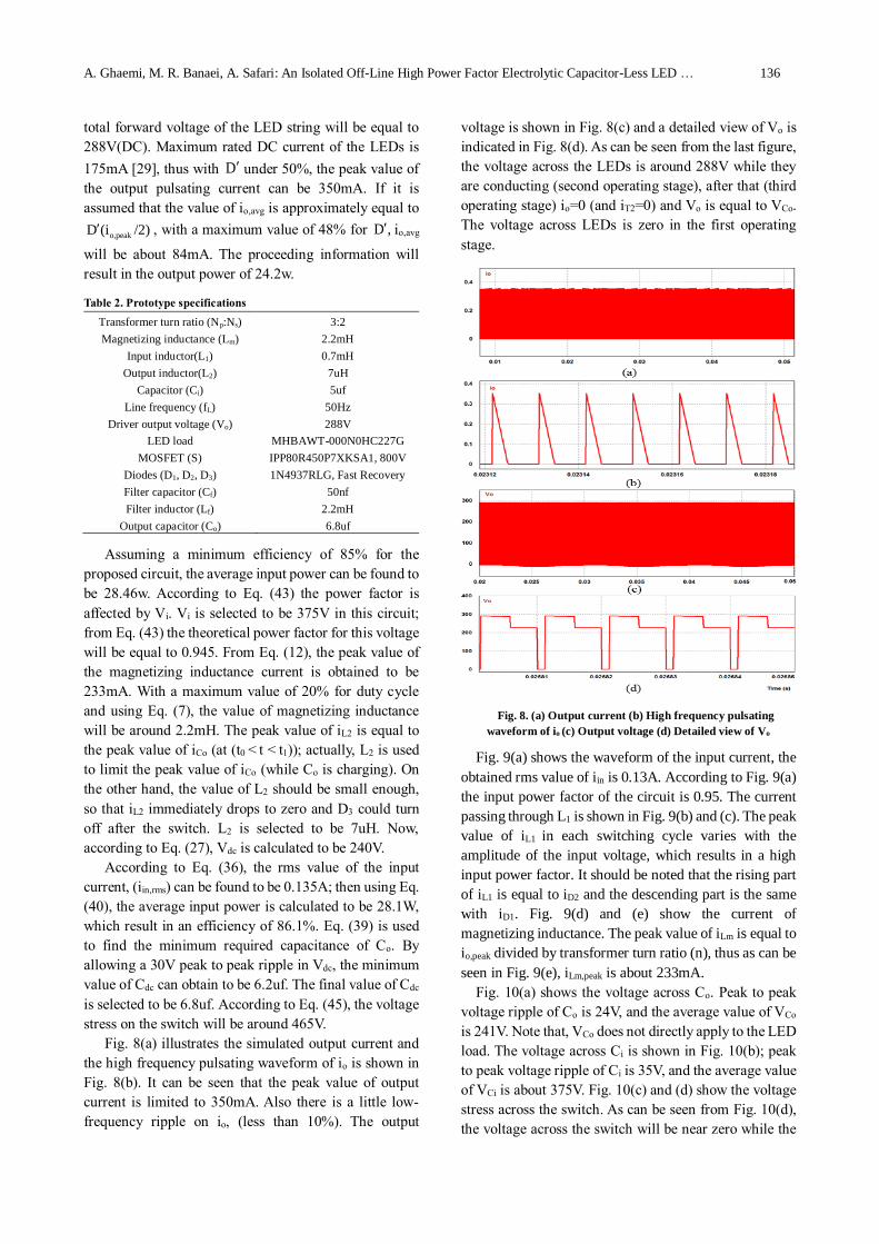
Fig. 9(a) shows the waveform of the input current, the
obtained rms value of iin is 0.13A. According to Fig. 9(a)
the input power factor of the circuit is 0.95. The current
passing through L1 is shown in Fig. 9(b) and (c). The peak
value of iL1 in each switching cycle varies with the
amplitude of the input voltage, which results in a high
input power factor. It should be noted that the rising part
of iL1 is equal to iD2 and the descending part is the same
with iD1. Fig. 9(d) and (e) show the current of
magnetizing inductance. The peak value of iLm is equal to
io,peak divided by transformer turn ratio (n), thus as can be
seen in Fig. 9(e), iLm,peak is about 233mA.
Fig. 10(a) shows the voltage across Co. Peak to peak
voltage ripple of Co is 24V, and the average value of VCo
is 241V. Note that, VCo does not directly apply to the LED
load. The voltage across Ci is shown in Fig. 10(b); peak
to peak voltage ripple of Ci is 35V, and the average value
of VCi is about 375V. Fig. 10(c) and (d) show the voltage
stress across the switch. As can be seen from Fig. 10(d),
the voltage across the switch will be near zero while the

Journal of Operation and Automation in Power Engineering, Vol. 7, No. 1, May 2019 137
switch is in ON state (first operating stage). Vsw for the
OFF state of the switch can be found using Eq. (45);
which is the maximum voltage stress across the switch
(second operating stage). At last (in the third operating
stage), Vsw will be equal to VCi.
Fig. 9. (a) Input current (b) Current waveform of L1 (c) Detailed
view of iL1 (d) Current waveform of Lm (e) Detailed view of iLm
Fig. 10. (a) Voltage across the output capacitor (b) Voltage across
Ci (c) Voltage stress across the switch (d) Detailed view of Vsw
According to the designed LED driver, a prototype has
been built and tested successfully. Fig. 11 shows the
measured experimental waveforms of the proposed
driver. The output current and voltage, the current
passing L1, the voltage across Ci and Co, the voltage stress
across the switch and the input voltage and current are
presented in Fig. 11.
Fig. 11. Experimental waveforms of the prototype
The total time interval for the illustrated waveform of
the output current is equal to a few line cycles. The low-
frequency ripple of the current through the LEDs is
measured to be 13.9%. The peak to peak voltage ripple

A. Ghaemi, M. R. Banaei, A. Safari: An Isolated Off-Line High Power Factor Electrolytic Capacitor-Less LED … 138
value is around 35V for VCi and 25V for VCo. The
maximum voltage stress across the switch is measured to
be around 470V.
The measured power factor of the constructed circuit
is 0.948 which is in good agreement with the proceeding
analysis and simulation results. The maximum voltage
stress across the switch (or switches) for the proposed
circuit and some recent structures are shown in Fig.12.
These values show the voltage stress across the switches
in the same conditions (regarding the input voltage and
the voltage of the DC link). As can be seen, the proposed
circuit has a better position in this comparison. With the
measured input power of 28.1w and output power of
24.2w, the efficiency of the driver will be equal to 86.1%.
Fig.13 shows the photograph of the prototype.
Fig. 12. Voltage stress comparison (the ** sign shows the voltage
stress for the proposed circuit)
Fig. 13. Photograph of the prototype
4. CONCLUSIONS
This paper has proposed an innovative isolated LED
driver with high frequency pulsating driving current. The
driver ensures a high input power factor and low, output
low-frequency ripple which is illustrated over the
simulations and experimental results of the paper.
Reduction of the output low-frequency ripple, make it
possible to remove the electrolytic capacitor from the
driver structure; by eliminating the electrolytic capacitor
the lifetime of the proposed LED driver better matches
the lifetime of LED semiconductors. The PFC action and
output current regulation have done just by using a single
switch and a simple controlling approach. The operating
stages, calculations and detailed analysis of the proposed
LED driver have been discussed in this paper.
Design example has been provided, and an
experimental prototype has been built to verify the
validity of the proposed LED driver. The implemented
circuit is a 24.2w, 288V(DC output) driver with 220V,
50Hz AC input.
REFERENCES [1] D. A. Steigerwald et al., “Illumination with solid state
lighting technology,” IEEE J. Sel. Top. Quantum Electron., vol. 8, no. 2, pp. 310–320, 2002.
[2] Haijin Liao, Yonghai Yu, and Xiaojian Liu, “The research of humanized design of the LED landscape lighting lamp,” 2009 IEEE 10th Int. Conf. Comput-Aided. Ind. Design Conceptual Des., 2009, pp. 499–502.
[3] D.-H. Yoo and G.-Y. Jeong, “LCD panel sector-dimming controlled high efficiency LED backlight drive system,” 2009 Int. Conf. Electr. Mach. Syst., 2009, pp. 1–6.
[4] “International standard IEC 1000-3-2 Class C. LED,” Mar-1995.
[5] E. Energy Star, “ENERGY STAR ® Program Requirements for Solid State Lighting Luminaires.”
[6] B. Lehman, A. Wilkins, S. Berman, M. Poplawski, and N. Johnson Miller, “Proposing measures of flicker in the low
frequencies for lighting applications,” 2011 IEEE Energy Convers. Congress Exposition, 2011, pp. 2865–2872.
[7] A. Wilkins, J. Veitch, and B. Lehman, “LED lighting flicker and potential health concerns: IEEE standard PAR1789 update,” 2010 IEEE Energy Convers. Congress Exposition, 2010, pp. 171–178.
[8] Evox Rifa electrolytic capacitors, “Electrolytic Capacitors Application Guide,” Espoo, Finland, 2001.
[9] “Lifetime of White LEDs, Energy Efficiency and Renewable Energy,” U.S.Dept. Energy, Washington DC, 2009.
[10] L. Han and N. Narendran, “An Accelerated Test Method for Predicting the Useful Life of an LED Driver,” IEEE Trans. Power Electron., vol. 26, no. 8, pp. 2249–2257, Aug. 2011.
[11] M. Nassary, M. Orabi, E. M. Ahmed, E. S. Hasaneen, and
M. Gaafar, “Modified harmonic injection technique for electrolytic capacitor-less LED driver,” 2017 19th Int. Middle-East Power Syst. Conf. MEPCON 2017 - Proc., vol. 2018–Febru, no. December, pp. 1459–1464, 2018.
[12] J. Baek and S. Chae, “Off-line buck LED driver for series connected LED segments,” Conf. Proc. - IEEE Appl. Power Electron. Conf. Expo. - APEC, pp. 1506–1510, 2017.
[13] Hyun-Su Gu and Sang-Kyoo Han, "A current-balancing modular driver for multi-channel LEDs," 8th IET Int. Conf. Power Electron. Mach. and Drives (PEMD 2016), Glasgow, 2016, pp. 1-6.
[14] H. Wu, S. C. Wong, and C. K. Tse, “A More Efficient PFC Single-Coupled-Inductor Multiple-Output Electrolytic Capacitor-less LED Driver With Energy-Flow-Path Optimization,” IEEE Trans. Power Electron., vol. PP, no. c, pp. 1–1, 2018.
[15] H.-Y. Park, B.-J. Seo, K.-S. Park, K.-S. Kang, and E.-C. Nho, “Electrolytic capacitor-less high-brightness LED

Journal of Operation and Automation in Power Engineering, Vol. 7, No. 1, May 2019 139
driving AC/DC converter for LED performance degradation reduction,” Electron. Lett., vol. 54, no. 10, pp. 648–649, 2018.
[16] K. Park, B. Seo, K. Kang, and E. Nho, “An AC-DC Power Converter for Electrolytic Capacitor-less LED Driver with
High Luminous Efficacy,” 2018 Int. Power Electron. Conf. (IPEC-Niigata 2018 -ECCE Asia), pp. 922–926, 2018.
[17] B. White, Y. F. Liu, and X. Liu, “A control technology to achieve a low cost flicker-free single stage LED driver with power factor correction,” 2015 IEEE 16th Work. Control Model. Power Electron. COMPEL 2015, 2015.
[18] Q. Hu and R. Zane, “Minimizing Required Energy Storage
in Off-Line LED Drivers Based on Series-Input Converter Modules,” IEEE Trans. Power Electron., vol. 26, no. 10, pp. 2887–2895, Oct. 2011.
[19] P. Fang, W. Sam, Y. F. Liu, and P. C. Sen, “Single-stage LED Driver Achieves Electrolytic Capacitor-less and Flicker-free Operation with Unidirectional Current Compensator,” IEEE Trans. Power Electron., vol. 8993, no. c, 2018.
[20] P. Fang and Y. F. Liu, “Single stage primary side controlled offline flyback LED driver with ripple cancellation,” in 2014 IEEE Appl. Power Electron. Conference and Exposition - APEC 2014, 2014, pp. 3323–3328.
[21] P. Fang, B. White, C. Fiorentino, and Y.-F. Liu, “Zero ripple single stage AC-DC LED driver with unity power factor,” in 2013 IEEE Energy Convers. Congress Exposition., 2013, pp. 3452–3458.
[22] Y. Qiu, H. Wang, Z. Hu, L. Wang, Y.-F. Liu, and P. C. Sen, “Electrolytic-capacitor-less high-power LED driver,” in 2014 IEEE Energy Convers. Congress Exposition (ECCE), 2014, pp. 3612–3619.
[23] H. Valipour, G. Rezazadeh, and M. R. Zolghadri, “Flicker-
free electrolytic capacitor-less universal input offline LED driver with PFC,” IEEE Trans. Power Electron., vol. 31, no. 9, pp. 6553–6561, 2016.
[24] Y. Qiu, L. Wang, Y.-F. Liu, and P. C. Sen, “A novel bipolar series Ripple compensation method for single-stage high-power LED driver,” in 2015 IEEE Appl. Power Electron.Conf. Exposition (APEC), 2015, pp. 861–868.
[25] S. Buso, G. Spiazzi, M. Meneghini, and G. Meneghesso,
“Performance Degradation of High-Brightness Light Emitting Diodes Under DC and Pulsed Bias,” IEEE Trans. Device Mater. Reliab., vol. 8, no. 2, pp. 312–322, Jun. 2008.
[26] M.-S. Lin and C.-L. Chen, “An LED Driver With Pulse Current Driving Technique,” IEEE Trans. Power Electron., vol. 27, no. 11, pp. 4594–4601, Nov. 2012.
[27] A. Note, “Application note: Pulsed Over-Current Driving
of Cree ® XLamp ® LEDs: Information and Cautions Introduction,” pp. 1–11, 2016.
[28] J. C. W. Lam and P. K. Jain, “A high power factor, electrolytic capacitor-less AC-input LED driver topology with high frequency pulsating output current,” IEEE Trans. Power Electron., vol. 30, no. 2, pp. 943–955, 2015.
[29] “Cree ® XLamp ® MHB-A LEDs,” Prod. Fam. data sheet, 2017.