
AN INTRODUCTION TO RS485
21
DIPARTIMENTO DI FISICA AN INTRODUCTION TO RS485 Abstract: RS 485 specification has been discussed in the present Technical Reports. TABLE OF CONTENTS INTRODUCTION .......................................................................................................................................................... 2 LINE LENGTH ............................................................................................................................................................... 5 GROUNDING THE SYSTEM ........................................................................................................................................ 6 TERMINATIONS .......................................................................................................................................................... 8 TRANSIENT OVERVOLTAGE PROTECTION ........................................................................................................... 16 CIRCUIT BOARD LAYOUT AND PROTECTION DEVICE PLACEMENT ............................................................... 19 brought to you by CORE View metadata, citation and similar papers at core.ac.uk provided by AIR Universita degli studi di Milano
Transcript of AN INTRODUCTION TO RS485

DIPARTIMENTO DI FISICA
AN INTRODUCTION TO RS485
Abstract: RS 485 specification has been discussed in the present Technical Reports.
TABLE OF CONTENTS
INTRODUCTION .......................................................................................................................................................... 2
LINE LENGTH ............................................................................................................................................................... 5
GROUNDING THE SYSTEM ........................................................................................................................................ 6
TERMINATIONS .......................................................................................................................................................... 8
TRANSIENT OVERVOLTAGE PROTECTION ........................................................................................................... 16
CIRCUIT BOARD LAYOUT AND PROTECTION DEVICE PLACEMENT ............................................................... 19
brought to you by COREView metadata, citation and similar papers at core.ac.uk
provided by AIR Universita degli studi di Milano

~ 2 ~
DIPARTIMENTO DI FISICA
INTRODUCTION
Industrial and instrumentation applications require transmission of data between multiple systems
often over very long distances. However, in many specific applications the maximum requested
distance is of about few meters even if in more recent application a shorter distance can be used.
The RS-485 bus standard is one of the most widely used physical layer bus designs in the
aforementioned applications. The key features of RS-485 (based on the Standard ANSI TIA/EIA-
485-A) that make it ideal for use in these communications applications are:
Long distance links—up to 1200 m.
Bidirectional communications possible over a single pair of twisted cables.
Differential transmission increases noise immunity and decreases noise emissions.
Multiple drivers and receivers can be connected on the same bus.
Wide common-mode range allows for differences in ground potential between the driver
and receiver.
TIA/EIA-485-A allow for data rates of up to 10 Mbps. Devices meeting the TIA/EIA-485-A
specifications do not have to operate over the entire range and are not limited to 10 Mbps.
This type of bus is mainly used in the following applications: process control networks, industrial
automation, remote terminals, building automation, such as heating, ventilation, air conditioning
(HVAC), security systems, motor control and motion control.
The main reason why RS-485 can communicate over long distances is the use of differential or
balanced lines. A communication channel requires a dedicated pair of signal lines to exchange
information. The voltage on one line equals the inverse of the voltage on the other line. Standard
ANSI TIA/EIA-485-A designates the two lines in this differential pair as A and B. Line A is more
positive than Line B (VOA > VOB) on the driver output if a logic high is received on the input of the
transmitter (DI = 1). If a logic low is received on the input of the transmitter (DI = 0), the transmitter
causes Line B to be more positive than Line A (VOB > VOA).
The typical value obtained for RS485 are here reported:

~ 3 ~
DIPARTIMENTO DI FISICA
TABLE 1 – LOGIC VALUE AND MEASURED VOLTAGE IN RS485 (RT=120 , RA=RB=750 , A CONNECTED TO GND AND B CONNECTED TO
VCC).
Function Logic value Signal Measured Voltage V
Transmission mode
1 DE = 1 VA = 4.3 V
2 V TX = 1 VB = 1.3 V
0 DE = 1 VA = 1.2 V
- 3.2 V TX = 0 VB = 4.4 V
Receiving mode
N.A.
DE = 0 VA = 2.4 V
- 0.4 V VB = 2.8 V
A differential signaling interface circuit consists of a driver with differential outputs and a receiver
with differential inputs. This circuit has increased noise performance because the noise coupling
into the system is equal on both signals. One signal emits the opposite of the other signal and
electromagnetic fields cancel each other. This reduces the electromagnetic interference (EMI) of
the system.
The driver generates, as shown in Figure 1, complementary voltages on A and B lines. Figure 1
shows how EIA-485-A defines VOA, VOB, and VO. When VOA is low, VOB is high and obviously when
VOA is high, VOB is low. Most physical parts (i.e. integrated circuit) also have the ability to tri-state
both A and B. It is important to note that signals A and B are complementary, but this does not
imply that one signal is a current return for the other in fact RS- 485 is not a current loop.
The drivers and receivers must share a common ground as depicted in figure. Receivers are de-
signed to respond to the difference between A and B. VO is the differential voltage. Receivers must
be sensitive to a 200-mV difference between VOA and VOB. Anything less than 200 mV is
indeterminate.
FIGURE 1 - DRIVER OPERATION.

~ 4 ~
DIPARTIMENTO DI FISICA
RS 485 SIGNALS
In the following Figure is reported the top view pin-out of the integrated circuit (ISL41847 from
INTERSIL) used for RS485.
FIGURE 2 – TOP VIEW PIN-OUT OF THE ISL81487.
An RS-485 system must have a driver that can be disconnected from the transmission line when a
particular node is not transmitting. The DE (RTS) pin on the RS-485 transceiver enables the driver
when a logic high is set to DE (DE = 1). Setting the DE pin to low (DE = 0) puts the driver in a tri-
state condition. This effectively disconnects the driver from the bus and allows other nodes to
transmit over the same twisted pair cable.
The RS-485 used transceivers have also an RE pin that enables/disables the receiver. The DE and
RE pins combined allow some RS-485 transceivers to be put into a low power shutdown mode.
This is important for battery-powered applications. The following tables give the thru table for the
used device [1].
FIGURE 3 – TRUTH TABLE FOR ISL81487 [1].

~ 5 ~
DIPARTIMENTO DI FISICA
The minimum operating circuit is reported in figure.
FIGURE 4 – TYPICAL OPERATING CIRCUIT [1].
In case of multi-point half-duplex RS485 link the following configuration is used.
FIGURE 5 – TYPICAL OPERATING CIRCUIT FOR HALF-DUPLEX RS-485 BUS CONFIGURATION [2].
This configuration is also known as a 2-wire RS-485 network connected in a multipoint configuration
and allows for data transmission in both directions, but only in one direction at a time.
LINE LENGTH
When high data rates are used, the application is limited to a shorter cable. It is possible to use
longer cables when low data rates are used. The dc resistance of the cable limits the length of the
cable for low data rate applications by increasing the noise margin as the voltage drop in the cable
increases. The ac effects of the cable limit the quality of the signal and limit the cable length to
short distances when high data rates are used.
More in details the following aspects need to be considered.

~ 6 ~
DIPARTIMENTO DI FISICA
The two slopes result from different limitations. The maximum cable length is the result of the
voltage divider that the cable’s DC loop resistance and the termination resistance create. For
differential buses, the loop resistance is twice as high as you might expect, because both conductors
in the pair equally contribute.
The curve’s sloped portion results from AC limitations of the drivers and the cable.
The following Figure can be used as a conservative guide for cable length vs. data rate [2].
Please note that in many cases the application operate at data rate less than 90 kbps. In particular,
often the 9600 bps rate (in the past also the rate 4800 bps have been used) and 19200 bps are used.
FIGURE 6 - CABLE LENGTH VS. DATA RATE
GROUNDING THE SYSTEM
In order to better understand how to ground the system it is necessary first to define the common
mode voltage (Vcm). Figure 7 shows how Vcm is defined. TIA/EIA-485-A states, “Common-mode
voltage (Vcm) is the sum of ground potential difference, generator (driver) offset voltage and
longitudinally coupled noise voltage.”
Vnoise is coupled identically onto both wires. The result is usually referred to as common-mode
noise. If a twisted pair is used, a useful simplification is to model Vnoise as common mode.
VGPD is the parameter that seems to cause the most problems. The problem stems from the over-
simplification that ground is a perfect conductor with null resistance, which is far from the truth.
In fact, earth ground potentials from circuit to circuit in an industrial installation can vary several
Low Rate applications

~ 7 ~
DIPARTIMENTO DI FISICA
volts under normal conditions.
FIGURE 7 - COMMON-MODE VOLTAGE AT THE RECEIVER.
These voltage most often stem from current leaking from equipment into the ground system.
However, during electrical activity, potentials between grounds in different parts of a building or
system can momentarily, for example, reach tens or hundreds of volts. Potentials between grounds
in different buildings or in different locations of the system can even reach thousands or hundreds
of thousands of volts. The practical ramification of this is that earth ground is a poor choice for
referencing signal grounds on distributed network nodes. The best method for control- ling VGPD is
to simply run a third wire for the purpose of referencing local signal grounds. The following figure
shows a solution often adopted.
FIGURE 8 - GROUNDING THE SYSTEM.
The common-mode voltage (Vcm) allowable between drivers and receivers on an RS-485 network is
+12 to –7 V. This setup provides 7 V of protection from each rail (assuming systems supplied at
5V). When the common-mode voltage on a node drifts beyond the allowable Vcm of +12 to –7 V,
~ 8 ~
DIPARTIMENTO DI FISICA
the node is no longer guaranteed to function. In fact, the drivers and receivers in the node may be
subject to damage.
The adopted solution for RS485 bus make available the following wires:
Line A, signal
Line B, signal
GND, ground (for grounding the system)
Vcc = 5 V (reserved).
TERMINATIONS
In a transmission line, there are two wires, one to carry the currents from the driver to the receiver
and another to provide the return path back to the driver. RS-485 links are a little more complicated
because of the fact that they have two signal wires that share a termination as well as a ground
return path.
For reliable RS-485 communications, it is essential that the reflections in the transmission line be
kept as small as possible and this is possible only if a proper cable termination is present.
Reflections happen very quickly during and just after signal transitions. On a long line, the
reflections are more likely to continue long enough to cause the receiver to misread logic levels.
On short lines, the reflections occur much sooner and have no effect on the received logic levels.
Terminating a data cable with a resistor having value equal to the cable characteristic impedance
reduces reflections that could cause data errors. However, if the data rate is low and/or the cable
is particularly short termination may be not necessary. As data rates increase termination be-
comes important and often mandatory. Generally speaking, since any device on the bus can
transmit, it is probable that a node within the middle of the bus will transmit requiring that
termination be applied to both ends of the bus segments. In fact, RS-485 applications require
termination at the master node and the slave node furthest from the master. Several options are
available for terminating an RS485 bus. The following Table shows a comparison of different
termination techniques.

~ 9 ~
DIPARTIMENTO DI FISICA
TABLE 2 - TERMINATION ADVANTAGES AND DISADVANTAGES [2].
a) WITHOUT TERMINATION: The time required for a signal to propagate down the line to a receiver
determines if a line is considered a transmission line. Physically long wires have longer
propagation times, whereas physically short wires have shorter propagation times. When the
propagation time is short relative to the data bit duration, the effect on the signal quality is
minimized. A cable is not seen as a transmission line if the signal rise time is more than four
times the propagation delay of the cable.
b) PARALLEL TERMINATION: When two or more drivers share a pair of wires, each end of the link has a
termination resistor equal to the characteristic impedance of the cable. There should be no
more than two terminating resistors in the network regardless of how many nodes are
connected (see Figure 9 where only the case of a differential driver sending information to a
differential receiver is reported. The case of bidirectional line is discussed in the following). In a
half-duplex configuration, both ends of the cable must be terminated. In a full duplex
configuration only the master receiver and most remote slave receiver need to be terminated,
as shown in Figure 5. This is the most popular solution for termination and it is known also as
DC termination. Resistive termination have typically values of 120 although twisted-pair cable
impedances can be as low as 100 . Please note that the 100 value is too small for EIA-485
drivers.
FIGURE 9 - PARALLEL OR DC TERMINATION.
c) AC TERMINATION: AC termination is used to reduce the power consumption of idle links as well
as to reduce ringing voltages. The negative effect though is a reduction in cable length and bit
rate. A resistor and capacitor can be placed in series across the bus (between A and B) as
shown in Figure 5. The Capacitor CT is selected in function of both the delay introduced by the
cable and the characteristic impedance of the cable, i.e. it is not possible to calculate a
capacitance value valid for all the applications.

~ 10 ~
DIPARTIMENTO DI FISICA
FIGURE 10 - AC TERMINATION.
Another popular option is a modified parallel termination that also provides a fail-safe bias. A
detailed discussion of fail-safe biasing occurs later in the next Section and will be not further
discussed in this Section. Figure 11 compares the four popular termination methods. The main point
to remember is that, if you use termination, you should locate the termination networks at the
two extreme ends of the cable, not at every node [3].
FIGURE 11 - RS-485 BUSES CAN USE FOUR METHODS OF TERMINATION. ACHIEVING THE BEST ELECTRICAL PERFORMANCE REQUIRES AC-
CEPTING HIGHER POWER DISSIPATION IN THE TERMINATION RESISTORS [3].
It is possible to evaluate the situation from a quantitative point of view.
There are several rules of thumb to follow when predicting if the line is long enough to be a
transmission line.
The first very good rule of thumb consider that if the propagation delay of the data is much less
than one bit width termination is mandatory. This rule make the assumption that reflections will
damp out in several trips up and down the data line. Since the receiving UART will sample the data
in the middle of the bit, it is important that the signal level be solid at that point. For example, in a
system with 600 m of data line the propagation delay can be evaluated by multiplying the cable
length by the propagation velocity of the cable. This value, typically 66 to 77 % of the light speed,
is specified by the cable manufacturer. For example, a round trip cover 1200 m of cable. Using a
propagation velocity of 66% c, one round trip is completed in approximately 6.2 s. If we assume
the reflection will damp out in three “round trips” up and down the cable length, the signal will
stabilize in 18.6 s after the leading edge of a bit. At 9600 baud one bit is 104 s wide. Since the

~ 11 ~
DIPARTIMENTO DI FISICA
reflections are damped out much before the center of the bit, termination is not mandatory.
However, the termination can be used in order to meet the requirement also in different situation
in particular when noise is present (as often in industrial applications).
In the following figure two different waveform are shown: at the left the signal without termination
is depicted whereas at the right the same signal with termination.
(A) (B)
FIGURE 12 - AN UNTERMINATED RS-485 WAVEFORM (A), COMPARED WITH A WAVEFORM OBTAINED FROM A CORRECTLY TERMINATED
NETWORK (B).
FAIL-SAFE BIASING
In Figure 13 a configuration of a master/slave RS-485 network with no fail-safe biasing is shown.
A synchronous data transmission is typically used in many industrial applications. A start bit
indicates the start of a bit sequence and is detected when a transition occurs from high to low. Eight
data bits and a parity bit follow the start bit. A stop bit that can be one or two bits long follows this
bit sequence. A following start bit starts the next bit sequence. When the last character is sent the
line should stay high until the next start bit. This causes problems in multipoint applications when
the transceivers connected on the bus are in receive mode simultaneously. This is known as a bus
idle condition and in this case, the differential voltage on the bus (VOA − VOB) is 0 V. Under this
condition, the receiver output (RO) is undefined by the RS-485 standard and, thus, the receiver
output can produce random data. This data is connected to the UART and can cause erroneous
system operation.

~ 12 ~
DIPARTIMENTO DI FISICA
FIGURE 13 - MASTER/SLAVE RS-485 NETWORK WITH NO FAIL-SAFE BIASING OF THE NETWORK.
The differential input threshold voltage (VTH) of a receiver is the voltage on the receiver input at
which a transition (low to high or high to low) of the receiver output is guaranteed. A typical RS-
485 transceiver has a differential input threshold voltage of ±200 mV. What this means is that
when the differential input is larger than or equal to 200 mV (VIA – VIB ≥ 200 mV), the receiver out-
put is guaranteed to be high (RO = 1). When the differential input is less than or equal to −200 mV
(VIA – VIB < −200 mV), the receiver output is guaranteed to be low (RO = 0). See Table 3 for a truth
table for the receiver.
TABLE 3 - DIFFERENTIAL RECEIVER TRUTH TABLE.
In FIGURE 14 report the value for unbalanced lines A and B. typical values are 3.68 V for high
level and 1.48 V for low level (RT=120 , RA=RB=560 , A connected to Vcc and B connected to GND).
In this way VAB = 2.2 V when VA >VB and VAB = - 2.2 V when VA
<VB.
In Figure 15 waveform for balanced line at the driver and at the receiver are shown. Typ ica l
values for applications are:

~ 13 ~
DIPARTIMENTO DI FISICA
FIGURE 14 – WAVEFORM FOR UNBALANCED LINES A AND B (REFERRED TO GND) [5].
(A)
(B)
FIGURE 15 – WAVEFORM FOR DRIVER (A) AND RECEIVER (B) [6].
During the bus idle condition, there is no device driving the bus. The receiver output is undefined.
This can cause random data to be received on the UART, which in turn can cause false start bits,

~ 14 ~
DIPARTIMENTO DI FISICA
false interrupts, and framing errors. This problem can be solved by placing a combination of pull-
up and pull-down resistors at one position on the bus. Figure 9 shows the biasing resistor circuit.
An example of calculating R1 and R2 is shown below (assume RT = 120 Ω):
R1 = R2 = R
VIA – VIB ≥ 200 mV
VIA – VIB = RT Vcc/(2R+RT) = 200 mV
if VCC = 5 V, then R = 1440 Ω
if VCC = 3 V, then R = 960 Ω
If lower values for R are used (VIA − VIB > 200 mV), a greater noise margin can be achieved in the
system. See Figure 16 for a graphical representation of the bus states and differential input volt-
age.
FIGURE 16 - FAIL-SAFE BIASING CIRCUIT.
FIGURE 17 - DIFFERENTIAL INPUT VOLTAGE.
It is important to highlights that new generation RS-485 transceivers have an improved feature
that includes true fail-safe receiver inputs. This eliminates the need for pull-up/pull-down resistors
as shown in the previous example. If a transceiver is specified to have a true fail-safe feature this
means that, the differential input threshold voltage (VTH) has been adjusted from ±200 mV to −200
mV to −30 mV (as shown in Figure 18). During the bus idle condition, VIA – VIB = 0 and therefore is

~ 15 ~
DIPARTIMENTO DI FISICA
larger than −30 mV, resulting in the receiver output being high (RO = 1). This means that if all
transceivers connected to the bus have true fail-safe features, the receiver output is always
defined. However, it is important to known that it is not always possible to known if all transceivers
connected to the bus have true fail-safe features, in particular when devices are connected with
devices of other manufacturer.
FIGURE 18 - INPUT THRESHOLD VOLTAGE.
TOPOLOGY
Figure 19 shows several network topologies. When the signals on the network are slow, the bit
edges are long, and the cable runs are short, topology is not an issue. Considering both the data
rate and the line length in bus different topologies can be probably used. However it is better to
consider as discussed in the following.
As soon as transmission line effects begin to show up, there is only one simple topology for man-
aging them. This is not to say, for example, that it’s impossible to implement a star configuration
with RS-485 devices. However, the best and simpler way to ensure a robust and reliable RS-485
network is to build it around a daisy-chain configuration. In fact, only the daisy chain is easy to
manage reflections on.

~ 16 ~
DIPARTIMENTO DI FISICA
FIGURE 19 - COMMON NETWORK TOPOLOGIES.
TRANSIENT OVERVOLTAGE PROTECTION
In industrial applications, lightning strikes, power source fluctuations, inductive switching, and
electrostatic discharge can cause damage to RS-485 transceivers by generating large transient
voltages. Starting from these considerations, as with any system design, consideration must be
given to the natural and induced environmental conditions to be encountered during operation.
Factory-controlled applications generally require protection against excessive noise voltages. The
noise immunity afforded by the differential transmission scheme, and, in particular, the wide
common-mode voltage range of 485, may be insufficient.
Many manufacturers offer a broad range of RS-485 devices with enhanced ESD protection such as
the ISL81487. This device has a “Built-In Driver Overload Protection”, a short circuit current limits,
and on-chip thermal shutdown circuitry. In particular, the driver output stages incorporate short
circuit current limiting circuitry which ensures that the output current never exceeds the RS-485
spec, even at the common mode voltage range extremes. Additionally, these devices utilize a
foldback circuit which reduces the short circuit current, and thus the power dissipation, whenever
the contending voltage exceeds either supply.
However, sometimes internal protection are not sufficient.
The level of protection can be, at this aim, further enhanced when using external clamping devices,
such as TVS diodes (see the typical circuit in Figure 20 where the voltage and parts are also de-
scribed).

~ 17 ~
DIPARTIMENTO DI FISICA
FIGURE 20
The protection is accomplished by clamping the voltage spike to a limit, by the low impedance
avalanche breakdown of a PN junction. TVS diodes are ideally open-circuit devices. A TVS diode can
be modeled as a large resistance in parallel with some capacitance while working below its break-
down voltage. When a transient is generated and the surge voltage is larger than the breakdown
voltage of the TVS, the resistance of the TVS decreases to keep the clamping voltage constant. The
TVS clamps the pulse to a level that does not damage the device that it is protecting. The transients
are clamped instantaneously (< 1 ns) and the damaging current is diverted away from the
protected device. In the Figure 21 characteristic of a unidirectional TVS diode is shown whereas in
Figure 22 the characteristic of a bidirectional TVS diode is also reported.
FIGURE 21 – I-V CHARACTERISTIC FOR TVS DIODE.

~ 20 ~
DIPARTIMENTO DI FISICA
FIGURE 22 - I-V CHARACTERISTIC FOR TVS DIODE.
The function of a TVS in RS-485 applications is to clamp the voltage on the bus to the common-
mode voltage range of the RS-485 transceiver (−7 V to +12 V). Some TVS devices have been
specifically designed for RS-485 applications. For higher power transients, protection can be
increased by adding Resistors RS (between 10 Ω and 20 Ω) between the protected device and
the input pin as shown in the following figure.
FIGURE 23
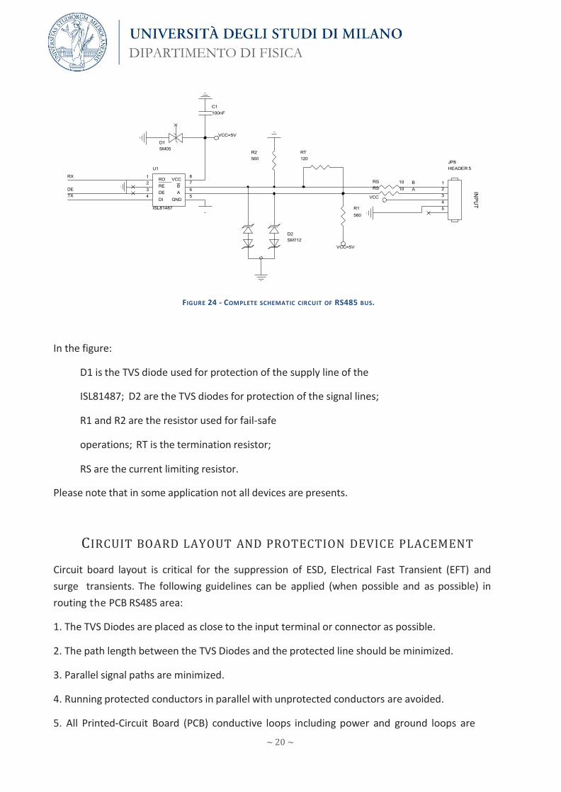
The complete solution for overvoltage protection is reported in the following figure.
~ 20 ~
DIPARTIMENTO DI FISICA
FIGURE 24 - COMPLETE SCHEMATIC CIRCUIT OF RS485 BUS.
In the figure:
D1 is the TVS diode used for protection of the supply line of the
ISL81487; D2 are the TVS diodes for protection of the signal lines;
R1 and R2 are the resistor used for fail-safe
operations; RT is the termination resistor;
RS are the current limiting resistor.
Please note that in some application not all devices are presents.
CIRCUIT BOARD LAYOUT AND PROTECTION DEVICE PLACEMENT
Circuit board layout is critical for the suppression of ESD, Electrical Fast Transient (EFT) and
surge transients. The following guidelines can be applied (when possible and as possible) in
routing the PCB RS485 area:
1. The TVS Diodes are placed as close to the input terminal or connector as possible.
2. The path length between the TVS Diodes and the protected line should be minimized.
3. Parallel signal paths are minimized.
4. Running protected conductors in parallel with unprotected conductors are avoided.
5. All Printed-Circuit Board (PCB) conductive loops including power and ground loops are
INP
UT

~ 20 ~
DIPARTIMENTO DI FISICA
minimized.
6. The length of the transient return path to ground are minimized.
7. The use of shared transient return paths to a common ground point are avoided.
8. Ground planes should be used whenever possible. For multilayer PCBs, ground vias are used.

~ 21 ~
DIPARTIMENTO DI FISICA
REFERENCES
[1] ISL81487 Datasheet, July 31, 2006, FN6050.7, Intersil.
[2] Hein Marais, RS-485/RS-422 Circuit Implementation Guide, AN-960 - APPLICATION NOTE, Rev. 0, 2008 Analog
Devices, Inc.
[3] John Goldie, Ten Ways to Bulletproof RS-485 Interfaces, National Semiconductor, Application Note 1057, Oc-
tober 1996.
[4] Bob Perrin, The Art and Science of RS-485, FEATURE ARTICLE, CIRCUIT CELLAR® ONLINE, July 1999,
www.circuitcellar.com.
[5] TUTORIAL 763 : Guidelines for Proper Wiring of an RS-485 (TIA/EIA-485-A) Network, Nov 19, 2001,
http://www.maximintegrated.com/an763, Maxim.
[6] Application Note. RS-422 and RS-485. Revised october 1997, B &B Electronics Mfg. Co. Inc., Ottawa, IL, 61350,
USA, www. bb-elec.com.