An Introduction to Carbon Nanotubes John Sinclair.
19
An Introduction to Carbon Nanotubes John Sinclair
-
Upload
cory-woods -
Category
Documents
-
view
227 -
download
2
Transcript of An Introduction to Carbon Nanotubes John Sinclair.

An Introduction to Carbon Nanotubes
John Sinclair

Outline
History Geometry
Rollup Vector Metallicity
Electronic Properties Field Effect Transistors Quantum Wires
Physical Properties Ropes
Separation

Introduction
High Aspect Ratio Carbon nanomaterial Family inclues Bucky
Balls and Graphene Single Wall Carbon
Nanotubes (SWCNT) Multiwall Carbon
Nanotubes (MWCNT)

History
1952 L. V. Radushkevich and V. M. Lukyanovich 50 nm MWCNT Published in Soviet Journal of
Physical Chemistry Cold War hurt impact of discovery Some work done before 1991 but not a “hot” topic
1991-1992 The Watershed Iijima discovers MWCNT in arc burned rods
Mintmire, Dunlap, and White‘s predict amazing electronic and physical properties
1993 Bethune and Iijima independently discover SWCNT Add Transition metal to Arc Discharge method
(same method as Bucky Balls)

Geometry
Rollup Vector (n,m) n-m=3d
Chiral Angle tan(θ) =
√3m/(2√(n2+m2+nm))
Arm Chair (n,n), θ=30 ○
Zig-zag (n,0), θ=0 ○
Chiral, 0○< θ<30 ○

Field Effect Transistors
FETs work because of applied voltage on gate changes the amount of majority carriers decreasing Source-Drain Current
SWCNT and MWCNT used Differences will be discussed
Gold Electrodes Holes main carriers
Positive applied voltage should reduce current

SWCNT Transport Properties
Current shape consistent with FET
Bias VSD = 10 mA G(S) conductance varies
by ~5 orders of magnitude
Mobility and Hole concentration determined to be large
Q=CVG,T (VG,T voltage to deplete CNT of holes)
C calculated from physical parameters of CNT
p=Q/eL

MWCNT Transport Properties
MWCNT performance is poor without defects See arrow for twists
in collapsed MWCNT MWCNT has
characteristic shape of FET
Hole density similar to SWCNT but Mobility determined to be higher Determined same as
above
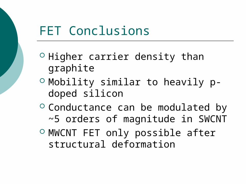
FET Conclusions
Higher carrier density than graphite Mobility similar to heavily p-doped
silicon Conductance can be modulated by
~5 orders of magnitude in SWCNT MWCNT FET only possible after
structural deformation

Quantum Wires
SWCNT Armchair tubes
SWCNT deposited over two electrodes Electrode
resistance determined with four point probe and found to be ~ 1 MΩ

Coulomb Charging
Contact Resistance Lower than Rquantum=h/e2~26 kΩ
C very low s.t. EC=e2/2C very large If EC <<kT, Current
only flows when Vbias>EC
Various gate V taken into account
Step-like conductance

Quantum Wire
Strongly Temperature dependent conduction curve
Occurs when a discrete electron level tunnels resonantly though Ef of electrode
If electron levels of SWCNT where continuous peak would be constant
E levels separated by ΔE The resonant tunneling
implies that the electrons are being transported phase coherently in a single molecular orbital for at least the distance of the electrodes (140 nm)

Physical Properties of Ropes
SWCNT rope laid on ultra-filtration membrane
AFM tip applies force to measure Shear Modulus G and Reduced Elastic Modulus Er Er = Elastic Modulus
when Searing is negligible
Displacement of tube/Force was measured and Er and G where calculated

Summary of Results
Typical Values Gdia ~ 478 GPa
Ggla ~ 26.2 GPa
Er-dia ~ 1220 GPa
Er-gla ~ 65-90 GPa

Conclusion On Physical Properties
Shear properties of SWCNT lacking (Even compared to MWCNT ropes)
Elastic properties very promising

Synthesis and Seperation
One major reason CNT devices have been so hard to scale up to industry uses is due to the inability to efficiently separate different species of CNT Different types are produced randomly with 1/3
conducting 2/3 semiconducting It has now been reported that with the
use of structure-discriminating surfactants one can isolate a batch of CNT such that >97% CNT within 0.02 nm diameter

Overview of Technique
Surfactants change buoyancy properties of CNT
Ultra-centrifugation techniques (which are scale-able) are used to separate different CNT
Effective separation is seen Separation according to metallicity Separation according to diameter

Conclusion
CNT devices show promise in molecular electronics both as wires and FET
Physical properties are very promising being both strong and light
Separation techniques continue to be developed to allow companies to make CNT devices

Sources
M. S. DRESSELHAUS, G. DRESSELHAUS, and R. SAITO. Carbon 33, 7 (1995)
R. Martel, T. Schmidt, H. R. Shea, T. Hertel, and Ph. Avourisa. App. Phys. Lett. 73, 17 (1998)
Sander J. Tans, Michel H. Devoret et al. Nature 386, 474-477 (1997)
Jean-Paul Salvetat et al. Phys. Rev. Lett. 82, 5 (1999) MICHAEL S. ARNOLD et al. Nature Nanotechnology 1,
60-65 (2006) www.noritake-elec.com/.../nano/structu.gif http://en.wikipedia.org/wiki/Carbon_nanotube academic.pgcc.edu/~ssinex/nanotubes/graphene.gif nano.gtri.gatech.edu/Images/MISC/figure4.gif