Intelligent Measurement Processes in 3D Optical Metrology ...

An Integrated System of Optical Metrology for Deep Sub-Micron Lithography
byXinhui Niu
B.S. (University of Science and Technology of China, Hefei, China) 1990M.S. (University of Notre Dame, Notre Dame, IN) 1994
A dissertation submitted in partial satisfaction of the
requirements for the degree of
Doctor of Philosophy
in
Engineering - Electrical Engineering and Computer Sciences
in the
GRADUATE DIVISION
of the
UNIVERSITY of CALIFORNIA, BERKELEY
Committee in charge:
Professor Costas J. Spanos, ChairProfessor Andrew R. Neureuther
Professor David Brillinger
Spring, 1999

The dissertation of Xinhui Niu is approved:
Chair Date
Date
Date
University of California, Berkeley
Spring, 1999

An Integrated System of Optical Metrology for Deep Sub-Micron Lithography
Copyright © 1999
by
Xinhui Niu

1
Abstract
An Integrated System of Optical Metrology for Deep Sub-Micron Lithography
by
Xinhui Niu
Doctor of Philosophy in Engineering - Electrical Engineering and Computer Sciences
University of California, Berkeley
Professor Costas J. Spanos, Chair
The exponential increase of integrated circuit density and semiconductor manufacturing
cost can be described by Moore’s Law. In order to provide affordable lithography at and
below 100nm, in-situ and in-line metrology must be used with off-line metrology for
advanced process control and rapid yield learning. This thesis develops an optical metrol-
ogy system for both unpatterned and patterned wafers in the deep sub-micron lithography
processes.
For unpatterned wafers, the most important observables for metrology are the thickness and
the optical properties and of the related thin-films. In this thesis, dispersion models
derived from the Kramers-Kronig relations are used with a simulated annealing optimiza-
tion procedure. Simulated annealing algorithms designed for continuous variables are
implemented. Spectroscopic reflectometry and spectroscopic ellipsometry are used to char-
acterize both solids and polymers. A statistical enhancement strategy is proposed based on
computational experimental design and Bayesian variable screening techniques to over-
come the large metrology dimension problem. A bootstrap method is introduced for testing
the accuracy of the characterization. Accurate information about the optical properties and
thickness is essential to many process control applications, and is the foundation to the suc-
cess of metrology for patterned wafers.
For patterned wafers, the most important observables are the profiles of the patterned fea-
tures. Profile information is critical in understanding the nature of the lithography process.
n k

2
However, it has been difficult to use because of the metrology cost. To solve this problem,
this thesis introduces the concept of specular spectroscopic scatterometry. Specular spec-
troscopic scatterometry uses conventional spectroscopic ellipsometers to extract the pro-
files of 1-D gratings. Based on a rigorous electromagnetic diffraction theory, the Grating
Tool-Kit (gtk) is developed to predict the behavior of a wide variety of diffraction gratings
with high precision. A library-based CD profile extraction methodology is presented and
validated with a focus-exposure matrix experiment. It is shown that specular spectroscopic
scatterometry is an accurate, inexpensive and non-destructive CD profile metrology.
The theme of this thesis is that, through the aid of computation and intelligent metrology,
more process information can be extracted from existing sensors, and the complexity of
expensive hardware can be shifted to sophisticated data analysis. It is expected that the pro-
posed metrology system will help the process control applications for the entire lithography
sequence.
Professor C. J. Spanos
Committee Chairman

iii
Table of Contents
Chapter 1Introduction. . . . . . . . . . . . . . . . . . . . . . . . . . . . . . . . . . . . . . . . . . . . . . . . . . . . . . . . . . .1
1.1 Motivation . . . . . . . . . . . . . . . . . . . . . . . . . . . . . . . . . . . . . . . . . . . . . . . . . . . . . . .11.2 Thesis Organization. . . . . . . . . . . . . . . . . . . . . . . . . . . . . . . . . . . . . . . . . . . . . . . .3
Chapter 2Background . . . . . . . . . . . . . . . . . . . . . . . . . . . . . . . . . . . . . . . . . . . . . . . . . . . . . . . . . . .7
2.1 Introduction to DUV Optical Lithography . . . . . . . . . . . . . . . . . . . . . . . . . . . . . .72.1.1 Chemically Amplified Resist . . . . . . . . . . . . . . . . . . . . . . . . . . . . . . . . . . . . . . . . . . . . . . . . . . . 82.1.2 Exposure Tools . . . . . . . . . . . . . . . . . . . . . . . . . . . . . . . . . . . . . . . . . . . . . . . . . . . . . . . . . . . . . 92.1.3 Optical Lithography Modeling . . . . . . . . . . . . . . . . . . . . . . . . . . . . . . . . . . . . . . . . . . . . . . . . . 9
2.2 Review of Metrology in Lithography Process. . . . . . . . . . . . . . . . . . . . . . . . . . .102.2.1 Spectroscopic Reflectometry . . . . . . . . . . . . . . . . . . . . . . . . . . . . . . . . . . . . . . . . . . . . . . . . . . 102.2.2 Spectroscopic Ellipsometry . . . . . . . . . . . . . . . . . . . . . . . . . . . . . . . . . . . . . . . . . . . . . . . . . . . 112.2.3 Fourier Transform Infrared Spectroscopy . . . . . . . . . . . . . . . . . . . . . . . . . . . . . . . . . . . . . . . . 132.2.4 SEM . . . . . . . . . . . . . . . . . . . . . . . . . . . . . . . . . . . . . . . . . . . . . . . . . . . . . . . . . . . . . . . . . . . . . 142.2.5 CD-AFM . . . . . . . . . . . . . . . . . . . . . . . . . . . . . . . . . . . . . . . . . . . . . . . . . . . . . . . . . . . . . . . . . 162.2.6 Scatterometry . . . . . . . . . . . . . . . . . . . . . . . . . . . . . . . . . . . . . . . . . . . . . . . . . . . . . . . . . . . . . . 162.2.7 Electrical Test for CD Measurement . . . . . . . . . . . . . . . . . . . . . . . . . . . . . . . . . . . . . . . . . . . . 16
2.3 A Schematic Flow of the Metrology in this Thesis . . . . . . . . . . . . . . . . . . . . . . .17
Chapter 3Simulated Annealing for Continuous Variable Optimization . . . . . . . . . . . . . . . . .22
3.1 Introduction . . . . . . . . . . . . . . . . . . . . . . . . . . . . . . . . . . . . . . . . . . . . . . . . . . . . .223.2 Basics of Simulated Annealing . . . . . . . . . . . . . . . . . . . . . . . . . . . . . . . . . . . . . .243.3 Simulated Annealing Algorithms for Continuous Variables. . . . . . . . . . . . . . . .26
3.3.1 Conventional Simulated Annealing (CSA) . . . . . . . . . . . . . . . . . . . . . . . . . . . . . . . . . . . . . . . 263.3.2 Fast Simulated Annealing (FSA) . . . . . . . . . . . . . . . . . . . . . . . . . . . . . . . . . . . . . . . . . . . . . . . 273.3.3 Generalized Simulated Annealing (GSA) . . . . . . . . . . . . . . . . . . . . . . . . . . . . . . . . . . . . . . . . 273.3.4 Adaptive Simulated Annealing (ASA) . . . . . . . . . . . . . . . . . . . . . . . . . . . . . . . . . . . . . . . . . . 28
3.4 Discussion . . . . . . . . . . . . . . . . . . . . . . . . . . . . . . . . . . . . . . . . . . . . . . . . . . . . . .32
Chapter 4Metrology for Unpatterned Thin-Films . . . . . . . . . . . . . . . . . . . . . . . . . . . . . . . . . . .36
4.1 Introduction . . . . . . . . . . . . . . . . . . . . . . . . . . . . . . . . . . . . . . . . . . . . . . . . . . . . .364.2 Electromagnetic Wave Propagation in a Stratified Medium . . . . . . . . . . . . . . . .404.3 Dispersion Models. . . . . . . . . . . . . . . . . . . . . . . . . . . . . . . . . . . . . . . . . . . . . . . .42
4.3.1 Cauchy Formulation. . . . . . . . . . . . . . . . . . . . . . . . . . . . . . . . . . . . . . . . . . . . . . . . . . . . . . . . . 434.3.2 Sellmeier Formulation . . . . . . . . . . . . . . . . . . . . . . . . . . . . . . . . . . . . . . . . . . . . . . . . . . . . . . . 43

iv
4.3.3 Effective Medium Approximation (EMA) . . . . . . . . . . . . . . . . . . . . . . . . . . . . . . . . . . . . . . . 434.3.4 Forouhi and Bloomer’s Formulation . . . . . . . . . . . . . . . . . . . . . . . . . . . . . . . . . . . . . . . . . . . . 444.3.5 Jellison and Modine’s Model. . . . . . . . . . . . . . . . . . . . . . . . . . . . . . . . . . . . . . . . . . . . . . . . . . 45
4.4 A Statistical Enhancement Strategy . . . . . . . . . . . . . . . . . . . . . . . . . . . . . . . . . .474.4.1 Statistical Experimental Design . . . . . . . . . . . . . . . . . . . . . . . . . . . . . . . . . . . . . . . . . . . . . . . . 484.4.2 Statistical Variable Screening . . . . . . . . . . . . . . . . . . . . . . . . . . . . . . . . . . . . . . . . . . . . . . . . . 484.4.3 Bootstrap Testing . . . . . . . . . . . . . . . . . . . . . . . . . . . . . . . . . . . . . . . . . . . . . . . . . . . . . . . . . . . 51
4.5 Polysilicon Characterization . . . . . . . . . . . . . . . . . . . . . . . . . . . . . . . . . . . . . . . .534.6 DUV Photoresist Characterization . . . . . . . . . . . . . . . . . . . . . . . . . . . . . . . . . . .564.7 Conclusions . . . . . . . . . . . . . . . . . . . . . . . . . . . . . . . . . . . . . . . . . . . . . . . . . . . . .58
Chapter 5Rigorous Numerical Analysis for Diffraction Gratings . . . . . . . . . . . . . . . . . . . . . .61
5.1 Introduction . . . . . . . . . . . . . . . . . . . . . . . . . . . . . . . . . . . . . . . . . . . . . . . . . . . . .625.2 Fundamental Properties of Diffraction Gratings . . . . . . . . . . . . . . . . . . . . . . . . .64
5.2.1 The Grating Equation. . . . . . . . . . . . . . . . . . . . . . . . . . . . . . . . . . . . . . . . . . . . . . . . . . . . . . . . 645.2.2 Wave Propagation in Periodic Structures . . . . . . . . . . . . . . . . . . . . . . . . . . . . . . . . . . . . . . . . 665.2.3 Diffraction Efficiency . . . . . . . . . . . . . . . . . . . . . . . . . . . . . . . . . . . . . . . . . . . . . . . . . . . . . . . 695.2.4 The Notations of the Grating Structure in This Thesis . . . . . . . . . . . . . . . . . . . . . . . . . . . . . . 705.2.5 Computational Categories of RCWA . . . . . . . . . . . . . . . . . . . . . . . . . . . . . . . . . . . . . . . . . . . 72
5.3 Fourier Transformation of Permittivity and Inverse Permittivity for 1D Gratings735.4 1D TE Polarization . . . . . . . . . . . . . . . . . . . . . . . . . . . . . . . . . . . . . . . . . . . . . . .765.5 1D TM Polarization. . . . . . . . . . . . . . . . . . . . . . . . . . . . . . . . . . . . . . . . . . . . . . .815.6 Numerical Solutions . . . . . . . . . . . . . . . . . . . . . . . . . . . . . . . . . . . . . . . . . . . . . .86
5.6.1 BLAS and LAPACK . . . . . . . . . . . . . . . . . . . . . . . . . . . . . . . . . . . . . . . . . . . . . . . . . . . . . . . . 875.6.2 Matrix Storage Format . . . . . . . . . . . . . . . . . . . . . . . . . . . . . . . . . . . . . . . . . . . . . . . . . . . . . . . 875.6.3 Blocked Gaussian Elimination Approach . . . . . . . . . . . . . . . . . . . . . . . . . . . . . . . . . . . . . . . . 88
5.7 Discussion of the Convergence Rate . . . . . . . . . . . . . . . . . . . . . . . . . . . . . . . . . .895.8 Discussion of gtk Performance . . . . . . . . . . . . . . . . . . . . . . . . . . . . . . . . . . . . . .97
Chapter 6Metrology for Patterned Thin-Films. . . . . . . . . . . . . . . . . . . . . . . . . . . . . . . . . . . . .104
6.1 Introduction . . . . . . . . . . . . . . . . . . . . . . . . . . . . . . . . . . . . . . . . . . . . . . . . . . . .1046.2 Specular Spectroscopic Scatterometry . . . . . . . . . . . . . . . . . . . . . . . . . . . . . . .1096.3 A Library-Based Methodology for CD Profile Extraction . . . . . . . . . . . . . . . .1146.4 Experimental Verification . . . . . . . . . . . . . . . . . . . . . . . . . . . . . . . . . . . . . . . . .1156.5 Conclusions . . . . . . . . . . . . . . . . . . . . . . . . . . . . . . . . . . . . . . . . . . . . . . . . . . . .126
Chapter 7Conclusion and Future Work . . . . . . . . . . . . . . . . . . . . . . . . . . . . . . . . . . . . . . . . . .130
7.1 Thesis Summary . . . . . . . . . . . . . . . . . . . . . . . . . . . . . . . . . . . . . . . . . . . . . . . .1307.2 Future Work. . . . . . . . . . . . . . . . . . . . . . . . . . . . . . . . . . . . . . . . . . . . . . . . . . . .131

v
Appendix ASymbols Used in Chapter 5 . . . . . . . . . . . . . . . . . . . . . . . . . . . . . . . . . . . . . . . . . . . .133
Appendix Bgtk . . . . . . . . . . . . . . . . . . . . . . . . . . . . . . . . . . . . . . . . . . . . . . . . . . . . . . . . . . . . . . . . .135
Appendix CThe TEMPEST Script Used in Section 5.8 . . . . . . . . . . . . . . . . . . . . . . . . . . . . . . . .139

vi
List of FiguresFigure 2.1 DUV lithography process sequence and wafer states...................................8Figure 2.2 Modeling flowchart of a lithography simulation........................................10Figure 2.3 Spectroscopic reflectometry measurements. ..............................................10Figure 2.4 Spectroscopic ellipsometry measurements.................................................12Figure 2.5 An example of cross-sectional SEM for CD profiles. ................................14Figure 2.6 Examples of CD-SEM scans on two different CD profiles........................15Figure 2.7 A schematic metrology flow in lithography processes. .............................17Figure 3.1 Trapped in a local minimum. .....................................................................23Figure 3.2 Basic Simulated Annealing Algorithm.......................................................25Figure 3.3 The effect of Temperature_Anneal_Scale on the parameter temperature.30Figure 3.4 The effect of Temperature_Ratio_Scale on the parameter temperature....31Figure 3.5 The effect of dimension on the parameter temperature.............................31Figure 3.6 Histogram of the parameter generated values with respect to the parameter
temperature. ............................................................................................32Figure 3.7 A hybrid optimization framework. .............................................................33Figure 4.1 Principle of data analysis for spectroscopic reflectometry and spectroscopic
ellipsometry. ...........................................................................................37Figure 4.2 The effect of logarithm transformation on tanΨ . .......................................39Figure 4.3 Wave propagates in a stack of thin-film.....................................................40Figure 4.4 Strategy of statistical enhancement on a metrology system.......................48Figure 4.5 Experimental thin-film with a polysilicon, silicon dioxide and silicon stack
and the uncertainty about the n and k of polysilicon from LPCVD. ......54Figure 4.6 (a) Posterior probability of polysilicon thickness with α = 0.2 and k = 10,
(b) Bootstrap testing of the enhanced metrology....................................55Figure 4.7 Relative reflectance curve fitting. ..............................................................55Figure 4.8 Empirical optical property decomposition of a DUV photoresist thin-film56Figure 4.9 Photoresist thin-film optical decomposition by simulated annealing. .......57Figure 4.10 Comparison between the experimental and theoretical ellipsometry data for
DUV photoresist on silicon.....................................................................57Figure 5.1 Phase relation of the diffracted rays in a grating........................................64Figure 5.2 0th order only diffraction. ..........................................................................66Figure 5.3 Wave propagates in a two-dimensional periodic medium. ........................67Figure 5.4 Geometric and cross-sectional notations of the 1-D grating problem........71Figure 5.5 Wave vector shows conical nature of diffraction in the 1-D conical
polarization. ............................................................................................73Figure 5.6 Symmetric gratings and non-symmetric gratings.......................................74Figure 5.7 Top-down cross-section view of a 1D grating. ..........................................74Figure 5.8 Test structures for RCWA convergence rate..............................................90Figure 5.9 The relation between the simulation time and the number of retained orders
in the structure of Figure 5.8.a. ...............................................................91

vii
Figure 5.10 Convergence vs. number of retained orders of the structure Figure 5.8.a at 248nm. ....................................................................................................92
Figure 5.11 Convergence vs. number of retained orders of the structure Figure 5.8.a at 632nm. ....................................................................................................92
Figure 5.12 Convergence vs. number of retained orders of the structure Figure 5.8.b at 248nm. ....................................................................................................92
Figure 5.13 Convergence vs. number of retained orders of the structure Figure 5.8.b at 632nm. ....................................................................................................93
Figure 5.14 Convergence vs. number of retained orders of the structure Figure 5.8.c at 248nm (resist loss is 30nm). ...................................................................93
Figure 5.15 Convergence vs. number of retained orders of the structure Figure 5.8.c at 632nm (resist loss is 30nm). ...................................................................93
Figure 5.16 Convergence vs. number of retained orders of the structure Figure 5.8.d at 248nm (resist loss is 10nm). ...................................................................94
Figure 5.17 Convergence vs. number of retained orders of the structure Figure 5.8.d at 632nm (resist loss is 10nm). ...................................................................94
Figure 5.18 Continuous grating profile is approximated by multilevel rectangular gratings....................................................................................................95
Figure 5.19 Convergence vs. number of retained orders of the structure Figure 5.18 at 248nm with 10 slices. .............................................................................95
Figure 5.20 Convergence vs. number of retained orders of the structure Figure 5.18 at 632nm with 10 slices. ............................................................................96
Figure 5.21 Convergence vs. number of retained orders of the structure Figure 5.18 at 248nm with 100 slices. ..........................................................................96
Figure 5.22 Convergence vs. number of retained orders of the structure Figure 5.18 at 632nm with 100 slices. ..........................................................................96
Figure 5.23 Test structure for comparing gtk with TEMPEST. ....................................97Figure 6.1 Configuration of the single wavelength variable angle scatterometry. ....106Figure 6.2 A simple grating structure for evaluating scatterometry on future
technologies. .........................................................................................107Figure 6.3 Simulation of the 0th and 1st order diffraction efficiency over the incident
angle for the 180nm technology. .........................................................108Figure 6.4 Simulation of the 0th order diffraction efficiency over the incident angle
for the 150nm technology. ....................................................................108Figure 6.5 Simulation of the 0th order diffraction efficiency over the incident angle
for the 100nm technology. ....................................................................109Figure 6.6 Optical properties of the Shipley UV5TM positive DUV photoresist. ....110Figure 6.7 Simulation of specular spectroscopic scatterometry for the 180nm
technology (θ=45°). ..............................................................................111Figure 6.8 Simulation of specular spectroscopic scatterometry for the 180nm
technology (θ=75°). ..............................................................................111Figure 6.9 Simulation of specular spectroscopic scatterometry for the 150nm
technology (θ=45°). ..............................................................................112

viii
Figure 6.10 Simulation of specular spectroscopic scatterometry for the 150nm technology (θ=75°). ..............................................................................112
Figure 6.11 Simulation of specular spectroscopic scatterometry for the 100nm technology (θ=45°). ..............................................................................113
Figure 6.12 Simulation of specular spectroscopic scatterometry for the 100nm technology (θ=75°). ..............................................................................113
Figure 6.13 A library based methodology for CD profile extraction. .........................114Figure 6.14 (a) Grating structures; (b) Focus-exposure matrix experiment setup for
experimental verification. .....................................................................116Figure 6.15 tanΨ of the entire F-E matrix. ..................................................................117Figure 6.16 cos∆ of the entire F-E matrix. ..................................................................117Figure 6.17 tanΨ of the fixed focus (-1) level and different dose levels
(from -3 to +3). .....................................................................................118Figure 6.18 cos∆ of the fixed focus (-1) level and different dose levels
(from -3 to +3). .....................................................................................118Figure 6.19 Calibrated CD AFM profile of the dose level -1 and focus level -1. .......119Figure 6.20 The optical properties of the ARC in the experiment. .............................120Figure 6.21 Measured and simulated tanΨ from the AFM CD profile. ......................120Figure 6.22 Measured and simulated cos∆ from the AFM CD profile........................121Figure 6.23 Residual plot of the measured and simulated tanΨ from the AFM
CD profile. ............................................................................................121Figure 6.24 Residual plot of the measured and simulated cos∆ from the AFM
CD profile. ............................................................................................122Figure 6.25 Random CD profile library generation.....................................................123Figure 6.26 Matching on the simulated and measured tanΨ signal.............................124Figure 6.27 Matching on the simulated and measured cos∆ signal. ............................125Figure 6.28 Comparison between the extracted CD profiles and the CD-AFM profile.125Figure 6.29 Comparison between the extracted grating profiles and the CD-AFM profiles
across the focus-exposure matrix. The four AFM profiles with (dose, focus) level of (2,-2), (3,-1), (-1,2) and (2,2) have not been measured.126
Figure B.1 A grating structure. ..................................................................................136Figure B.2 A Tcl code sample. ..................................................................................137Figure B.2 Computation result shows the effect of a grating structure on the
convergence rate. ..................................................................................137

ix
List of TablesTable 4.1 Comparison of the un-enhanced and enhanced metrology..........................55Table 4.2 F&B parameters of the three components in the DUV photoresist. ............57Table 5.1 1-D TM eigenvalue problem formulations in gtk........................................84Table 5.2 Optical properties of the material used in Figure 5.8. .................................90Table 5.3 Diffraction efficiency of the TE wave in the testing case calculated by gtk.98Table 6.1 Configuration parameters of Figure 6.2 for future technology generations.107Table B.1 1D grating commands ................................................................................135

x
Acknowledgments
Many people have assisted me in my education. I would like to first thank my advisor, Pro-
fessor Costas Spanos, for his guidance, support and encouragement during the last four and
half years. I thank him for encouraging me to wildly explore the research topics, from inter-
net computing to semiconductor metrology issues. Especially I thank him for the time he
spent on this thesis. I would like to thank Professor Andy Neureuther for his helpful sug-
gestion and invaluable comments on my research. Professor David R. Brillinger, who
served on my Qualifying Exam Committee, has been an excellent source of feedback con-
cerning many statistical aspects of this work. I also thank Professor Tsu-Jae King for serv-
ing as the Chair of my Qualifying Exam Committee.
I started to learn Berkeley NOW clustered processing from Professor David Patterson’s
IRAM class. Professor Jim Demmel provided a lot of advice on numerical analysis tech-
niques, and he facilitated access to NOW for two semesters. Krste Asanovic explained the
PhiPAC project, which gave me more insight about BLAS. Rich Vudoc offered help on
choosing the fine-tuned numerical libraries.
I thank Eric B. Grann for lending his Ph.D. thesis to me. I also thank Professor Jim
Moharam and Philippe Lalanne for answering several questions on RCWA over telephone
and e-mail.
I have received support from a lot of people in the semiconductor industry. I thank Joe
Bendik, Matt Hankinson, Bob Socha, Ron Kovacs of National Semiconductor for their
insights and collaboration. I am grateful to Cihan Tinaztepe of KLA-Tencor for the summer
internship in 1997. Craig MacNaughton and Anthea Ip of KLA-Tencor helped me with
some experimental measurements. I acknowledge Harry Levinson and Sanjay Yedur of
Advanced Micro Devices, Rick Dill of IBM Corporation, Scott Bushman, Robert Soper
and Stephanie Butler of Texas Instruments, and Piotr Zalicki of SC Technology, for their
support and help on many occasions.

xi
Berkeley Computer-Aided manufacturing (BCAM) is a very dynamic research group. I
would like to thank the past and present members of BCAM: Junwei Bao, Eric Boskin,
Runzi Chang, Roawen Chen, Sean Cunningham, Tim Duncan, Mark Hatzilambrou, Herb
Huang, John Musacchio, Tony Miranda, David Mudie, Anna Ison, Nickhil Jakatdar,
Soverong Leang, Jae-wook Lee, Sherry Lee, Mian Li, Jeff Lin, Greg Luurtsema, David
Mudie, Sundeep Rangan, Johan Saleh, Manolis Terrovitis, Nikhil Vaidya, Crid Yu, Haolin
Zhang, Dongwu Zhao. I would like to thank other people in Cory Hall: James Chen, Kai
Chen, Zhongshi Du, Heath Hoffmann, Lixin Su, Yiqun Xie.
I would like to thank Prof. Jay B. Brockman of University of Notre Dame. Jay introduced
me into the statistical computing area. I also thank my friends from Notre Dame: Yan Lin,
Jing Qiao, Minhan Chen, Helen Zhang, Hui Ye.
Special thanks go to Nickhil Jakatdar. There were so many “brainstorming” sessions, dis-
cussion and collaboration between us that have been incorporated in this thesis. I also thank
Sudnya Shroff, Nickhil’s wife, for her friendship. I thank Junwei Bao and Nickhil Jakatdar
for proof-reading my thesis. Tom Pistor helped me use TEMPEST.
I would like to deeply thank my friends in Berkeley: Fang Fang, Zhong Deng, Wei Li, Hui
Zhang, Tianxiong Xue, for their friendship, support and encouragement. I really feel that I
belong to a big warm family because of you.
Finally, I would like to express my special thanks to my family for their love and support.
My father, Anlin Niu, and my mother, Weidong Zhang, have always supported me and
have always been my role models. I would like to thank my sister Yanhui Niu and her hus-
band Xu Li. Without your love, this thesis would not be possible. I love all of you very
much.
This research has been sponsored by the Semiconductor Research Corporation (SRC), the
state of California Micro program, and participating companies (Advanced Micro Devices,
Applied Materials, Atmel Corporation, Lam Research, National Semiconductor, Silicon
Valley Group, Texas Instruments).

1
Chapter 1Introduction
1.1 Motivation
The evolution of integrated circuit (IC) technology has been governed mainly by device
scaling due to rapid technology development. The semiconductor market has grown at an
average rate of approximately 15% annually over the past three and a half decades [1.1].
Fueled by the continuing explosive growth of the semiconductor market, the introduction
of new technologies has been accelerated by leading semiconductor companies from the
traditional 3-year cycle towards an approximate 2-year cycle. However, the semiconductor
industry is facing increasingly difficult challenges as the feature sizes approach 100 nm.
One of the “grand challenges” is to make affordable lithography available at and below
100nm. For many years, as the key technology driver for semiconductor industry, optical
lithography has been the engine driving Moore’s Law. Lithography is also a significant
economic factor, currently representing over 35% of the chip manufacturing cost. With the
decrease in feature size required to follow Moore’s Law, lithography light sources have
progressed from the visible to the deep ultraviolet (DUV) wavelengths. Innovative wave-
front engineering techniques, such as off-axis illumination, optical proximity correction
and phase shifting mask, have been adopted to enable the industry to manufacture ICs with
feature sizes significantly smaller than the wavelength of the exposure light. Optical lithog-
raphy is becoming increasingly complicated and expensive.
Another “grand challenge” is to make affordable metrology and testing available. In current
technology, in-line or in-situ, non-destructive analysis of product wafers is preferable
whenever possible. The use of correct metrology will greatly improve the yield learning.

2
However, with the increasingly smaller dimensions and the need for greater purity, metrol-
ogy for processes such as lithography, etching and chemical mechanical polishing (CMP)
are becoming extremely difficult [1.2]. The increasing wafer size and decreasing feature
size makes metrology and testing very expensive. It may no longer be possible to rely on
sample measurements from wafer-to-wafer or die-to-die because of the measurement cost.
Hence, affordable and accurate metrology is necessary for the technology evolution.
Metrology in lithography processes is important to the entire fabrication process. The key
reason is the importance of controlling gate and interconnect linewidths and thicknesses.
Both gate delay and drive current are proportional to the inverse of the gate length. In cur-
rent deep submicron technology, the low level interconnect linewidths are approaching the
gate linewidth. The gate lengths have to be tightly controlled across chips and wafers so
that timing of signals can be well-correlated and placed in sequence. It is estimated that
1nm in channel critical dimension (CD) variation is equivalent to 1MHz chip-speed varia-
tion, and is thus worth about $7.50 in the selling price of each chip [1.3]. Yu et al. have
concluded that CD variation is mostly attributed to the lithography step, rather than other
process steps [1.4]. Process improvement for CD control requires the design and use of
novel metrology, which can monitor resist coat thickness and uniformity, photo-active
compound (PAC), photo-acid generator (PAG) and solvent concentration, pre/post bake
temperature effect uniformity, development uniformity, and final delivered CD. The driver
behind this proliferation of sensors is that significantly complicated interaction exists
among the processing conditions. Rich sensing data are more likely to capture this latent
information.
Optical metrology is often preferred in semiconductor manufacturing for many reasons.
Optical probes are usually non-destructive and non-invasive. Optical probes can be
deployed for real-time monitoring and control because of their low cost, small footprint,
high accuracy and robustness. This thesis will focus on the optical metrology design and
analysis.
In the lithography process, based on the specific process step, the metrology can be defined
for use on either unpatterned or patterned films; based on the types of observables, the
metrology can target either direct or indirect measurands. Direct measurands include the

3
physically existing properties which can be directly measured, such as thin-film thickness,
chemical composition, CD profile, etc. Indirect measurands include those characteristics
which must be extracted or interpreted from the measurement, such as optical properties
and , Technology Computer-Aided Design (TCAD) parameters, resist model parameters,
etc.
The goal of this thesis is to provide an affordable yet accurate metrology system for lithog-
raphy processing. In particular, the exponential increase in equipment cost by generation
will drive the need to prolong the useful equipment life of each generation in manufacturing
[1.5]. The theme of this thesis is that, through the aid of computation and intelligent metrol-
ogy, more process information can be extracted from existing sensors.
Even though the metrology system is designed for lithography processing, the technology
can be transferred to other processes, such as etching, CMP, etc. The objectives of the
metrology design are three-fold: the cost of equipment and manufacturing will be shifted
to the cost of computation as much as possible; sensors will be designed for in-line or in-
situ process control; the metrology will be applicable in current technology and also
extendable to future technology.
1.2 Thesis Organization
This thesis will present a systematic metrology system for unpatterned and patterned
wafers in the lithography process.
The thesis begins by providing a review of the DUV lithography process. Advanced resist,
resolution enhancement techniques, mask techniques, etc. all make optical lithography one
of the most challenging fields in the semiconductor industry. Then we review the current
metrology in the lithography process. A schematic flow of the metrology design in this
thesis is introduced at the end of Chapter 2.
Chapter 3 introduces simulated annealing, a global optimization technique, which is
heavily used in this work. Simulated annealing has become an often used tool to tackle hard
optimization problems in various fields of science. Its underlying idea of modeling the crys-
tal growth process in nature is easy to understand and simple to implement. However, the
n
k

4
performance of simulated annealing depends crucially on the annealing schedule. Simu-
lated annealing was introduced for combinatorial optimization, and successful in many
applications related to combinatorial optimization, such as the travelling salesman prob-
lem, VLSI computer-aided design (CAD), etc. Several simulated annealing algorithms for
functions of continuous variables are discussed and implemented. This powerful optimiza-
tion tool is the foundation of optical property extraction, resist model parameter extraction,
and other optimization problems when local minima exist.
Chapter 4 introduces the metrology for unpatterned thin-films. In this category, thin-film
thickness and the optical properties are the most important observables. Different materials
have different optical property characteristics; even the same material through different
process conditions has different optical property characteristics. Optical property is usually
described by a dispersion relation. There are several simple empirical dispersion formula-
tions, such as the Cauchy and the Sellmeier equations. However, in the DUV range, these
formulations fail for most materials. In this thesis work, dispersion formulations derived
from Kramers-Kronig relations are used with the aid of simulated annealing. A statistical
enhancement strategy is proposed based on computational experimental design and Baye-
sian variable screening to overcome the large metrology dimension problem. A bootstrap
method is introduced for testing the accuracy of simulated annealing. Two examples are
given to illustrate the metrology. The first example shows the thickness and optical prop-
erty extraction for polycrystalline silicon by using spectroscopic reflectometry. The second
example shows the DUV photoresist characterization by using spectroscopic ellipsometry.
The next two chapters present a novel scatterometry for patterned thin-films. The conven-
tional scatterometry prototype based on single wavelength, multiple incident or collect
angle leads to complicated equipment and is not scalable with technology. This thesis intro-
duces the specular spectroscopic scatterometry. “Specular” means that only 0th order dif-
fraction light needs to be measured, “spectroscopic” means that the measured light is
broadband, “scatterometry” means that diffraction gratings are used as the test structures.
The scattering behavior of diffraction gratings must be fully understood. Chapter 5
describes a rigorous theory for analyzing the diffraction gratings. The rigorous coupled-
wave analysis (RCWA) algorithms are summarized and implemented into a numerical

5
package. It is shown that the choice of correct RCWA formulation and number of retained
orders is essential to the simulation accuracy and speed.
Chapter 6 evaluates the design of specular spectroscopic scatterometry. The emphasis of
this design is to utilize existing optical metrology equipment. Specular spectroscopic scat-
terometry uses traditional spectroscopic ellipsometers to measure 1-dimensional gratings.
A library-based CD profile extraction methodology is presented. Experimental validation
has been performed with a focus-exposure matrix experiment. This metrology can be used
with current technology and is expected to be extended to the 0.1µm generation.
Finally, conclusions and future work related to this research are given in Chapter 7.

6
References for Chapter 1
[1.1] “The National Technology Roadmap for Semiconductors Technology Needs”,1997 Edition, Semiconductor Industry Association (SIA).
[1.2] “Metrology Roadmap: A Supplement to the National Technology Roadmap forSemiconductors”, SEMATECH, 1995.
[1.3] J. Sturtevant, et al, “CD control challenges for sub-0.25 µm patterning”, SEMAT-ECH DUV Lithography Workshop, Austin, TX, Oct. 16-18, 1996.
[1.4] C. Yu and C. J. Spanos, “Patterning tool characterization by causal variabilitydecomposition”, IEEE Transactions on Semiconductor Manufacturing, vol. 9, no.4, 527-535, Nov. 1996.
[1.5] G. E. Moore, “Lithography and the future of Moore’s law”, SPIE, vol. 2440, 2-17,Feb. 1995.

7
Chapter 2Background
In this chapter, optical lithography and related metrologies are briefly reviewed. The
important factors and observables in optical imaging and metrology are summarized. A
schematic flow of the metrology is presented at the end.
2.1 Introduction to DUV Optical Lithography
Lithographic scaling has historically been accomplished by optimizing the parameters in
the Rayleigh model for image resolution. The Rayleigh criterion for the minimum resolv-
able feature size is
(2.1)
and depth of focus is
(2.2)
where is the exposure wavelength and is the numerical aperture of the objective lens,
and are process dependent constants. To pattern devices with decreasing feature size,
photoresist exposure wavelengths were reduced and numerical apertures were increased.
However, the evolution of imaging systems is usually accompanied by a shrinking process
window, such as, a decrease in the allowed depth of focus and exposure latitude, and a cor-
responding decrease in overlay tolerance.
The DUV lithography process is illustrated in Figure 2.1. The lithography process consists
of many sequential modules such as the resist spin coat, soft bake, exposure, post-exposure
R
R k1λ
NA--------=
DOF
DOF k2λ
NA( )2---------------=
λ NA
k1 k2

8
bake and development. The DUV lithography process provides the process engineer with
numerous opportunities to monitor the process and wafer states. To design in-situ sensors
and metrology, it is important to understand these lithography modules and processing con-
stituents, such as materials (photoresist, developer and anti-reflection materials), process-
ing equipment (wafer track, stepper) and masks.
2.1.1 Chemically Amplified ResistThe chemical amplification concept was invented at IBM Research and was quickly
brought into use in production [2.1]. The need of chemical amplification in the DUV imag-
ing process is driven by the relatively low DUV light intensity available at the wafer plane
from exposure tools.
The classic near-UV positive resist consisting of a novolac resin and a photoactive diaz-
onaphthoquinone dissolution inhibitor does not perform adequately because of its exces-
sive unbleachable (i.e., inability to become more transparent during exposure) absorption
in the deep-UV region. The resist systems based on photochemical events that require sev-
eral photons to generate one useful product have inherently limited sensitivities.
In order to circumvent this intrinsic sensitivity limitation and to dramatically increase the
resist sensitivity, the concept of chemical amplification was proposed and reported in the
early 80’s by Ito, Willson and Frechet [2.2]. In chemically amplified resist systems, a cat-
alytic species generated by irradiation induces a cascade of subsequent chemical transfor-
Spin Coat&
Soft Bake
Exposure&
PEBDevelop
Thin-FilmPreparation
Figure 2.1 DUV lithography process sequence and wafer states.

9
mations, providing a gain mechanism. The use of acid as a catalyst has eventually become
the major foundation for the entire family of advanced resist systems, and the DUV lithog-
raphy is based on chemically amplified resists.
2.1.2 Exposure ToolsCoincident with the need to decrease optical wavelength to keep pace with resolution
requirements, there is a need to decouple resolution and overlay capability from increasing
field-size requirements. It appears that step-and-scan technology is dominant for the DUV
generation of production lithography equipment.
Traditionally, the lithographic requirements have been stated in terms of the key stepper
parameters of focus offset and exposure energy dose, often as an exposure-defocus process
window. Dose and focus are two of the most important variables for the stepper process
control.
2.1.3 Optical Lithography ModelingTechnology Computer-Aided Design (TCAD) tools are playing an important role in the
design and manufacturing of ICs. Accurate materials, process, and device modeling and
simulation are critical to timely, economic development of current and future integrated cir-
cuit technology. Reliance on experimental verification of process and device characteristics
is incompatible with the pace of technology advancement. To meet the “grand challenge”
of measurement requirements, IC manufacturing has to rely on more sophisticated comput-
ing techniques rather than expensive metrology equipment. As the cost of computation
decreases while the cost of experimentation and equipment increases, TCAD tools are
becoming essential cost effective alternatives. Simulation and modeling become indispens-
able tools for metrology design.
Optical lithography modeling began from the early work by F. H. Dill [2.3][2.4][2.5].
Sophisticated software that simulates the lithography processing were developed by vari-
ous researchers, including SAMPLE [2.6], PROLITH [2.7], and SOLID-C [2.9].
The effect of lithography process is studied by understanding the influence of the each pro-
cess step of Figure 2.1. Basic lithographic modeling steps include image formation, resist

10
exposure, post-exposure bake diffusion and development [2.8]. Corresponding models are
shown in Figure 2.2.
Most of these models are very complicated and highly nonlinear. Matching the simulation
results to the real measurement becomes a challenge because of nonlinearity and local min-
ima. A simulated annealing assisted approach is proposed and successfully deployed in this
thesis.
2.2 Review of Metrology in Lithography Process
2.2.1 Spectroscopic ReflectometryIn spectroscopic reflectometry, the reflected light intensities are measured in a broadband
wavelength range. In most setups, nonpolarized light is used at normal incidence. The big-
gest advantage of spectroscopic reflectometry is its simplicity and low cost. Figure 2.3
shows the setup of conventional spectroscopic reflectometry.
In reflectometry, only light intensities are measured. is the relation between the
reflectance and the complex reflection coefficient .
Aerial Image&
Standing Waves
Exposure Kinetics&
PEB DiffusionDevelop Kinetics
Figure 2.2 Modeling flowchart of a lithography simulation.
Figure 2.3 Spectroscopic reflectometry measurements.
R r 2=
R r

11
Spectroscopic reflectometry has been successfully developed for I-line lithography process
control [2.10]. Leang proposed a method to link the photoresist extinction coefficient to
Dill’s parameters through
(2.3)
where is the net absorption of the inhibitor, and is the net absorption of the base
resin, is the photoactive compound concentration. and are extracted from the
Cauchy dispersion relation by a nonlinear constrained local optimizer [2.11].
Although the idea of this work is novel, the computational method Leang proposed is not
suitable in the DUV regime for several reasons. First, the accuracy and usefulness of this
metrology depends on the accuracy of measured . Simple dispersion relations, such as the
Cauchy relation Leang used, can not be applied for many materials in the DUV range. Sec-
ond, local optimization techniques are not appropriate for complicated dispersion formula-
tions.
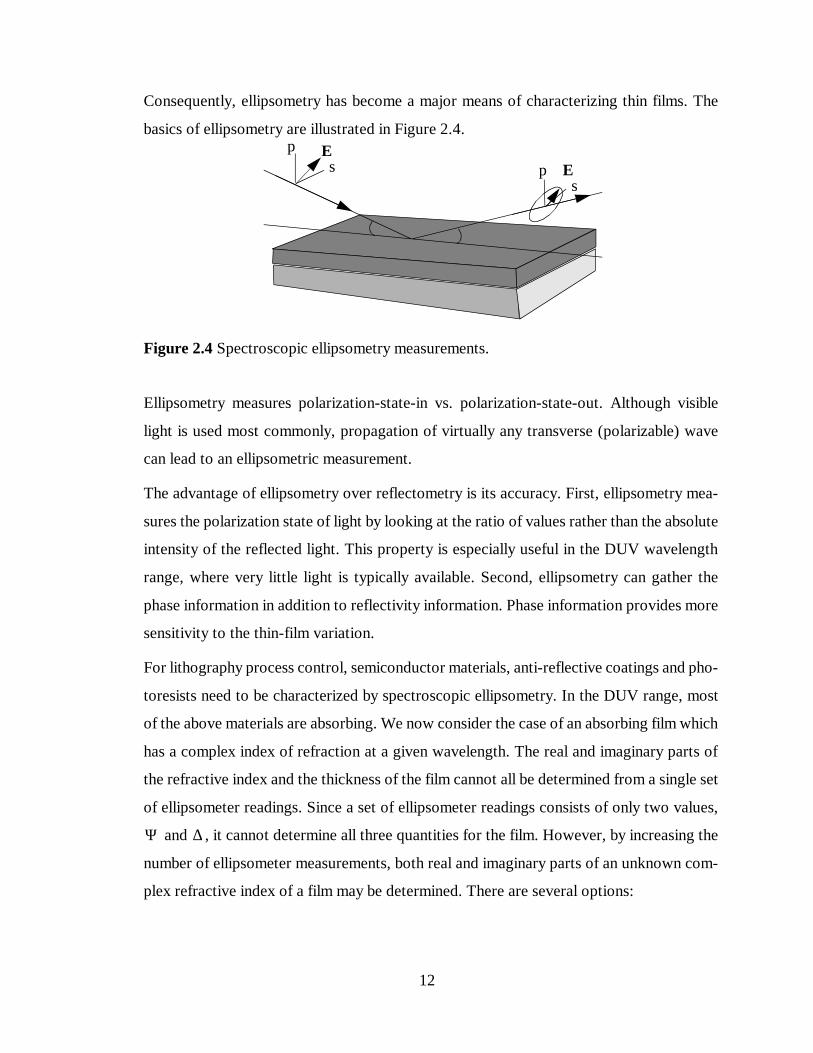
2.2.2 Spectroscopic EllipsometrySpectroscopic ellipsometry has become an essential metrology tool for the semiconductor
industry [2.12]. The component waves of the incident light, which are linearly polarized
with the electric field vibrating parallel (p or TM) or perpendicular (s or TE) to the plane
of incidence, behave differently upon reflection. The component waves experience differ-
ent amplitude attenuations and different absolute phase shifts upon reflection; hence, the
state of polarization is changed. Ellipsometry refers to the measurement of the state of
polarization before and after reflection for the purpose of studying the properties of the
reflecting boundary. The measurement is usually expressed as
(2.4)
where and the complex reflection coefficient for TM and TE waves.
Ellipsometry derives its sensitivity from the fact that the polarization-altering properties of
the reflecting boundary are modified significantly even when ultra-thin films are present.
k
k λA λ( )PAC B λ( )+4π------------------------------------------=
A λ( ) B λ( )PAC n k
k
ρ Ψtan ej∆ rprs----= =
rp rs
12
Consequently, ellipsometry has become a major means of characterizing thin films. The
basics of ellipsometry are illustrated in Figure 2.4.
Ellipsometry measures polarization-state-in vs. polarization-state-out. Although visible
light is used most commonly, propagation of virtually any transverse (polarizable) wave
can lead to an ellipsometric measurement.
The advantage of ellipsometry over reflectometry is its accuracy. First, ellipsometry mea-
sures the polarization state of light by looking at the ratio of values rather than the absolute
intensity of the reflected light. This property is especially useful in the DUV wavelength
range, where very little light is typically available. Second, ellipsometry can gather the
phase information in addition to reflectivity information. Phase information provides more
sensitivity to the thin-film variation.
For lithography process control, semiconductor materials, anti-reflective coatings and pho-
toresists need to be characterized by spectroscopic ellipsometry. In the DUV range, most
of the above materials are absorbing. We now consider the case of an absorbing film which
has a complex index of refraction at a given wavelength. The real and imaginary parts of
the refractive index and the thickness of the film cannot all be determined from a single set
of ellipsometer readings. Since a set of ellipsometer readings consists of only two values,
and , it cannot determine all three quantities for the film. However, by increasing the
number of ellipsometer measurements, both real and imaginary parts of an unknown com-
plex refractive index of a film may be determined. There are several options:
Figure 2.4 Spectroscopic ellipsometry measurements.
ps
Ep E
s
Ψ ∆

13
• A series of ellipsometer readings is obtained for films of different but unknown thick-
ness, with the same refractive index;
• Ellipsometer readings are obtained on a single film for different surrounding media of
known refractive index;
• Ellipsometer readings are obtained for a single film at various angles of incidence;
• Ellipsometer readings are obtained for a single film for multiple wavelengths. A known
formulation is needed to describe the refractive index over a range of wavelengths.
Variable Angle Spectroscopic Ellipsometry (VASE) tools are developed for this purpose
[2.13][2.14]. The data analysis techniques depend on the used dispersion relation formula-
tion. The method which commercial tools employ usually consists of two steps. First, the
film thickness and the real part of the index in the transparent region ( , usually in
the red or near infrared range) are extracted by a local optimization algorithm. Then, the
film thickness is used for both and extraction at shorter wavelengths where the film is
absorbing. The advantage of this approach is that it achieves unique solutions. In each step,
there are two unknowns and two measured parameters. The disadvantage is the inherent
lack of accuracy. Because the determination of the wavelength range where is quite
arbitrary, small errors of the film thickness extracted in the transparent region can be prop-
agated and magnified in the shorter wavelength region. In this thesis, we address this prob-
lem by using dispersion models derived from Kramers-Kronig relation and a global
optimization technique.
2.2.3 Fourier Transform Infrared SpectroscopyInfrared (IR) spectroscopy is the intensity measurement of the infrared light absorbed by a
sample. Infrared light is energetic enough to excite molecular vibrations to higher energy
levels. The wavelengths of IR absorption bands are characteristic of specific types of chem-
ical bonds, and IR spectroscopy finds its greatest utility in the identification of organic and
organometallic molecules. The IR spectrum of a compound is essentially the superposition
of absorption bands of specific functional groups, yet subtle interactions with the surround-
ing atoms of the molecule impose the stamp of individuality on the spectrum of each com-
pound. For qualitative analysis, one of the best features of an infrared spectrum is that the
n k 0=
n k
k 0=

14
absorption or the lack of absorption in specific wavelengths can be correlated with specific
stretching and bending motions of the molecular bonds and, in some cases, with the rela-
tionship of these groups to the remainder of the molecule. Thus, by interpretation of the
spectrum, it is possible to state that certain functional groups are present in the material and
that certain others are absent. FTIR has been demonstrated in the characterization of pho-
toresist thin films, including monitoring of solvent loss during the post-bake, determination
of the glass transition temperature, and deprotection reaction kinetics [2.15]. Many of these
applications depend on an accurate optimization procedure because the internal material
kinetics are very complicated and nonlinear. However, local optimization techniques were
applied in most publications. This usually requires a relatively good initial guess. Global
optimization techniques have been successfully applied in interpreting the FTIR measure-
ment by Jakatdar et al. [2.16].
2.2.4 SEMThe scanning electron microscope (SEM) is currently the instrument of choice in produc-
tion for measuring submicron-sized features because of its nanometer-scale resolution,
high throughput and precision. SEM includes both cross-sectional and top-down types.
Cross-sectional SEM can provide profile information for patterned features. Figure 2.5 is
an example of cross-sectional SEM. The advantage of cross-sectional SEM is that the
visual image can be immediately used for process characterization, the disadvantage is that
the measurement itself is destructive and time consuming, and the precise profiles depend
on the applied image processing techniques.
Figure 2.5 An example of cross-sectional SEM for CD profiles.

15
Top-down CD-SEM, as the name implies, is not a cross-sectional technique. CD-SEM
image intensity does not correspond directly to actual surface height. Techniques for deter-
mining the actual edge position from an intensity scan are somewhat arbitrary. The line-
width, or CD measurement can vary significantly depending on the edge detection
algorithm used. As an example, Figure 2.6 shows the SEM intensity scans of two grating
structures, measured by KLA-Tencor 8100XPTM CD-SEM. The two gratings are processed
from the same mask (280nm line and 560nm pitch) with different process conditions. Each
grating was measured twice at the same location. For the left grating, the repeated measure-
ment error is about 21.2nm; for the right grating, the repeated measurement error is about
0.3nm. The most appropriate algorithm and threshold must be determined by comparison
to a suitable reference tool. Also, the build-up of charge in the sample under the electron
beam is one of the most pervasive problems encountered in all of the applications of the
SEM.
In addition to the above limitation, CD-SEM can not provide film thickness information
and can not resolve undercut features. There are attempts to provide better estimates about
the feature shape from analyzing the CD SEM intensity scan signal [2.17]. However, the
accuracy of these approaches in lithography process characterization is unclear, because
different dose and focus settings usually generate considerably different CD film thickness
values.
Figure 2.6 Examples of CD-SEM scans on two different CD profiles.
scan1
scan2scan1
scan2

16
2.2.5 CD-AFMAtomic force microscopy (AFM) combines exceptional depth and lateral resolution to offer
a wealth of information about the resist feature’s width, wall angles, and thickness. AFM
is an excellent reference tool for other metrology [2.18]. Unfortunately, AFM scan rates are
currently very slow, and tip shape and stability have significant impact on measurement
accuracy and reproducibility. In addition, AFM analysis is often overly sensitive to local
film and sidewall roughness. At present, AFM is too slow to be used for real-time imaging
or high speed CD measurements.
2.2.6 ScatterometryScatterometry is the metrology which relates the geometry of a sample to its scattering
effects. The improved sensitivity and simplicity of diffraction were incorporated into pro-
cess monitoring by Kleinkecht, Bosenberg and Meier [2.19][2.20]. Electromagnetic scat-
tering and optical imaging issues related to linewidth measurement of polysilicon gate
structures were investigated in U. C. Berkeley by K. Tadros and A. R. Neureuther [2.21].
This is pioneering work in terms of using diffraction gratings for IC manufacturing. The
simulations were performed using normal incident TE polarized illumination by a rigorous
electromagnetic scattering simulator, TEMPEST [2.22]. However, the measurements were
collected using unpolarized illumination. For 1D grating, TE, TM and unpolarized incident
light have different diffraction effects.
Single-wavelength, variable-incident/collect angle scatterometry has been used to measure
periodic photoresist structures with relatively good agreement with other measurement
techniques [2.23][2.24]. The variable-angle design makes the equipment very expensive
and not easy for use in-situ. In this thesis, I propose the concept and design of specular spec-
troscopic scatterometry. Experiments and simulations show that specular spectroscopic
scatterometry can provide reliable cross-sectional profile information for the current and
future technology generations.
2.2.7 Electrical Test for CD MeasurementElectrical resistance measurements can be used to determine dimensions of line test struc-
tures that serve as proxies for actual devices [2.25][2.26][2.27]. Since test structures are

17
fabricated on the same wafer with actual devices, evaluating the measured resistance can
help determine the accuracy of lithography, etch, and other processes. Among the short-
comings of this method are lack of CD cross-sectional information, thin-film thickness
variation, effect of joule heating, etc.
2.3 A Schematic Flow of the Metrology in this Thesis
A series of metrology techniques is proposed in this thesis for DUV lithography. The
underlying theme throughout these techniques is low cost, ease of use for in-line or in-situ
deployment, and applicability for future generation of technology. Novel metrology is
designed and tested by using existing equipment. The cost of the equipment is shifted to
computation by a thorough understanding of the material modeling, lithography modeling,
intelligent use of testing structures, such as diffraction gratings, and intelligent use of test-
ing schemes, such as statistical experiment designs.
Spin Coat&
Soft Bake
Exposure&
PEBDevelop
Thin-FilmPreparation
Metrology for Unpatterned Film Metrology for Patterned FilmReflectometry
Ellipsometry
FTIR
Specular Spectroscopic Scatterometry
SEM and CD-SEM
CD-AFM
Figure 2.7 A schematic metrology flow in lithography processes.

18
The thin-film being measured can belong to either unpatterned or patterned film. Figure 2.7
shows the metrology flow in this thesis. Spectroscopic reflectometry and spectroscopic
ellipsometry are used for thickness and optical property characterization for unpatterned
thin-films, while optical properties can be further correlated to the processing conditions.
Spectral Spectroscopic Scatterometry is designed to evaluate the overall lithography per-
formance. In other words, it is used for photoresist profile characterization. The limitation
of spectral spectroscopic scatterometry is that it can only characterize periodic test struc-
tures. CD-SEM and CD-AFM can be used for non-periodic structures and as the reference
tools for scatterometry.

19
References for Chapter 2
[2.1] H. Ito, “Chemical amplification resists: History and development within IBM”,IBM J. Res. Develop. vol. 41, no. 1-2, 69-80, Jan/Mar. 1997.
[2.2] C. G. Willson, R. A. Dammel and A. Reiser, “Photoresist materials: a historicalperspective”, Proc. of SPIE, vol.3049, 28-41, 1997.
[2.3] F. H. Dill, “Optical lithography”, IEEE Trans. Electron Devices, ED-22, no. 7,440-444, 1975.
[2.4] F. H. Dill, W. P. Hornberger, P. S. Hauge and J. M. Shaw, “Characterization ofpositive photoresist”, IEEE Trans. Electron Devices, ED-22, no. 7, 445-452, 1975.
[2.5] F. H. Dill, A. R. Neureuther, J. A. Tuttle and E. J. Walker, “Modeling projectionprinting of positive photoresists”, IEEE Trans. Electron Devices, ED-22, no. 7,456-464, 1975.
[2.6] W. G. Oldham, S. N. Nadgaonkar, A. R. Neureuther, and M. M. O’Tole, “A gen-eral simulator for VLSI lithography and etching process: Part I - Applications toprojection lithography”, IEEE Trans. Electron Devices, vol. ED-26, no. 4, 717-722, 1979.
[2.7] C. A. Mack, “PROLITH: A comprehensive optical lithography model”, Proc. ofSPIE, vol. 538, 207-220, 1985.
[2.8] C. A. Mack, “Inside PROLITH, A Comprehensive Guide to Optical LithograhySimulation”, FINLE Technology, 1997.
[2.9] W. Henke, D. Mewes, M. Weiss, G. Czech, and R. Schiessl-Hoyler, “Simulationof defects in 3-dimensional resist profiles in optical lithography”, MicroelectronicEngineering, vol. 13, 497-501, 1991.
[2.10] S. Leang, S-Y Ma, J. Thomson, B. Bombay, and C. J. Spanos, “A control systemfor photolithographic sequences”, IEEE Trans. on Semiconductor Manufacturing,vol. 9, no. 2, 191-207, May 1996.
[2.11] S. Leang and C. J. Spanos, “A novel in-line automated metrology for photolithog-raphy”, vol. 9, no. 1, 101-107, IEEE Trans. on Semiconductor Manufacturing,February 1996.

20
[2.12] E. A. Irene, “Applications of spectroscopic ellipsometry to microelectronics”,Thin Solid Films, vol. 233, no. 1-2, 96-111, 1993.
[2.13] R. A. Synowicki, J. N. Hilfiker, C. L. Henderson, “Refractive index measurementsof photoresist and antireflective coatings with variable angle spectroscopic ellip-sometry”, Proc. of SPIE, vol. 3332, 384-390, 1998.
[2.14] P. Boher, J. L. Stehle, J. P. Piel and C. Defranoux, “Precise measurement of ARCoptical indices in the deep UV range by variable angle spectroscopic ellipsome-try”, Proc. of SPIE, vol. 3050, 205-214, 1997.
[2.15] R. Carpio, J. D. Byers, J. S. Petersen, W. Theiss, “Advanced FTIR techniques forphotoresist process characterization”, Proc. of SPIE, vol. 3050, 545-556, 1997.
[2.16] N. Jakatdar, X. Niu and C. J. Spanos, “Characterization of a chemically amplifiedphotoresist for simulation using a modified poor man’s DRM methodology”, Proc.of SPIE, vol. 3332, 578-585, 1998.
[2.17] J. M. McIntosh, B. C. Kane, J. B. Bindell and C. B. Vartuli, “Approach to CDSEM metrology utilizing the full waveform signal”, Proc. of SPIE, vol. 3332, 51-60, 1998.
[2.18] H. M. Marchman and N. Dunham, “AFM: a valid reference tool?”, Proc. of SPIE,vol. 3332, 2-9, 1998.
[2.19] H. P. Kleinknecht and H. Meier, “Linewidth measurement on IC masks andwafters by grating test patterns”, Applied Optics, vol. 19, 525-533, 1980.
[2.20] W. A. Bosenberg and H. P. Kleinknecht, “Linewidth measurement on IC wafersby diffraction from grating test patterns”, Solid State Technology, vol. 26, 79-85,July 1983.
[2.21] K. Tadros, A. R. Neureuther and R. Guerrieri, “Understanding metrology of poly-silicon gates through reflectance measurements and simulation”, Proc. of SPIE,vol. 1464, 177-186, 1991.
[2.22] A. Wong, “Rigorous Three-Dimensional Time-Domain Finite-Difference Electro-magnetic Simulation”, Ph.D. Dissertation, University of California at Berkeley,1994.

21
[2.23] J. R. McNeil, S. S. H, Naqvi, S. M. Gaspar, K. C. Hickman and others, “Scatter-ometry applied to microelectronics processing”, Solid State Technology, vol. 36,no. 3, 29-30, March 1993.
[2.24] C. J. Raymond, M. R. Murnane, S. L. Prins, S. S. H. Naqvi, J. R. McNeil, “Multi-parameter CD metrology measurement using scatterometry”, Proc. of SPIE, vol.2725, 698-709, 1996.
[2.25] T. Turner, “Electrical measurement of IC device CDs and alignment”, Solid StateTechnology, vol. 41, no. 6, 115-16, June 1998.
[2.26] C. Yu, “Integrated circuit process design for manufacturibility by statisticalmetrology”, Ph.D. Dissertation, U.C.Berkeley, 1996.
[2.27] M. Terrovitis, “Process variability and device mismatch”, Memorandum, no.UCB/ERL M96/29, 1996.

22
Chapter 3Simulated Annealing for Continuous
Variable Optimization
3.1 Introduction
Optimization problems occur in all areas of science and engineering, arising whenever
there is a need to minimize or maximize an objective function that depends on a set of vari-
ables, while satisfying some constraints. The optimization techniques can be classified as
either local or global. A local optimization algorithm is one that iteratively improves its
estimate of the minimum by searching for better solutions in a local neighborhood of the
current solution. Many local optimization techniques and related software packages have
been developed [3.1].
In many practical problems it is unknown whether the objective function is unimodal in the
desired region. The main weakness of local optimization algorithms is their inability to
escape from local minima. This is illustrated in Figure 3.1. The optimization process will
be trapped in local minima if the initial value is not chosen wisely. Therefore, methods
designed for global optimization are needed in these cases.
For handling global optimization problems, some new approaches have recently emerged,
inspired by physical phenomena. In particular, simulated annealing [3.2], genetic algo-
rithms [3.4], tabu search [3.5], and neural networks [3.6] have been successfully imple-
mented and used in many practical applications.
Kirkpatrick et al. introduced an optimization procedure which is referred to as “simulated
annealing (SA)” [3.3]. In this technique, one or more artificial temperatures are introduced

23
and gradually cooled, in complete analogy with the well-known annealing technique fre-
quently used in metallurgy for molten solid reaching its crystalline state. Annealing is the
process by which a material initially undergoes extended heating and then is slowly cooled.
Thermal vibrations permit a reordering of the atoms/molecules to a highly structured lat-
tice, or a low energy state.
The idea can be applied to optimization problems in the following way. First, a new point
is randomly sampled. If it generates a new minimum value, it is always accepted. If not, it
is accepted when a random number between 0 and 1 is less than a probability defined by a
mathematical function of temperature, usually the Boltzmann equation. Early in the itera-
tive process, the mathematical function generates values near 1, and most points are
accepted. By adjusting a temperature parameter in the probability function, smaller values
will be generated across successive cooling iterations, and eventually, only points that pro-
duce better solutions are accepted. Simulated annealing has been very successful in IC
CAD combinatorial optimization applications, such as standard-cell placement, global
routing and placement, gate-array placement, [3.7] [3.8] [3.9], etc. The success of the
method appears to be a consequence of exploring a large number of combinations, and of
the small probability of being trapped by local minima until late in the iterative process.
Extensive work has been done on extending simulated annealing ideas from combinatorial
problems to continuous functions, including Szu and Hartley [3.10], Ingber [3.11][3.12],
Tsallis and Stariolo [3.14], Corana et al. [3.15] and Siarry et al. [3.16], etc.
In the following sections, first we briefly discuss the basics of simulated annealing. Then
we will discuss several algorithms for continuous variable optimization, such as Conven-
Figure 3.1 Trapped in a local minimum.x
F(x)
globalminimum
localminimum
x0

24
tional Simulated Annealing (CSA), Fast Simulated Annealing (FSA), Generalized Simu-
lated Annealing (GSA), and Adaptive Simulated Annealing (ASA).
3.2 Basics of Simulated Annealing
The global optimization problem of concern is
(3.1)
where is a vector in -dimensional space , with elements . can be
either a continuous or a discrete variable. Given a state , the value of objective function
is also called the energy .
Most simulated annealing algorithms can be described by means of the pseudo-code shown
in Figure 3.2. There are five major components in SA implementation:
• Temperature sequence function . is the temperature parameter where is the
number of times the temperature parameter has changed. The initial value, , is gen-
erally relatively high, so that most changes are accepted and there is little chance of the
algorithm been trapped in a local minimum. is also called the “cooling schedule”,
which determines the reduction of the temperature parameter through the process of
optimization.
• Repetition function . This represents the number of searches at a temperature step
until some sort of “equilibrium” is approached.
• Probability density function of state-space of parameters. determines
how to generate a new state from the previous state. Usually depends on the tem-
perature, dimension of the parameter space, and some other factors.
• Probability function for acceptance of a new state given the previous state.
• Stopping criterion. This is to decide when the search will be terminated.
For combinatorial optimization problems, the variables are subject to discrete changes
only. For continuous optimization, the continuity has to be taken into account by suitably
minimize f x( ) subject to xi Ai Bi,[ ]∈
x D RD x1 x2 … xD, , ,( ) xi
x
E
Tk Tk k
T0
Tk
Lk
g x( ) D g x( )
g x( )
h ∆E Tk,( )

25
selected discretization steps: very small steps result in an incomplete exploration of the
variation domain with small and frequent function improvements; very large steps produce
too many unacceptable function variations.
Basic Simulated Annealing Algorithm
BeginInitialize ( , , , ) while ;Repeat
Repeat Generate state a neighbor to ;Calculate ;if Accept( , ) == true then
until ;;
Update ;Update ;
until StoppingCriterion == trueEnd
Subroutine Accept( , )if then return trueelse
if random(0,1) < ) then return true
else return false
endifendif
End
k Tk xi Lk k 0=
xj xi∆E Ej Ei–=∆E Tk xi xj=
Lkk k 1+=
LkTk
∆E Tk∆E 0≤
h ∆E Tk,( )
Figure 3.2 Basic Simulated Annealing Algorithm.

26
3.3 Simulated Annealing Algorithms for Continuous Variables
The challenge of simulated annealing is to cool the temperature as fast as possible, without
getting trapped in a local minimum. In other words, we want the fastest annealing schedule
which preserves the probability being equal to one of ending in a global minimum. Arbi-
trarily reducing the temperature will not guarantee a global minimum. We will discuss four
“rigorous” simulated annealing algorithms, CSA, FSA, GSA and ASA.
3.3.1 Conventional Simulated Annealing (CSA)Conventional Simulated Annealing is also called Boltzmann Annealing. The acceptance
probability is based on the chances of obtaining a new state with energy relative to
a previous state with energy ,
(3.2)
where .
An important aspect of simulated annealing is how to generate the ranges of the parameters
to be searched. Let be the deviation of from . CSA uses a Gaus-
sian distribution in the state generating function
. (3.3)
A logarithmic temperature schedule is consistent with the Boltzmann algorithm; the tem-
perature schedule is
. (3.4)
It has been proved that there exists an initial temperature large enough so that global
minimum can be obtained [3.13]. However, the logarithmic temperature schedule is rela-
tively slow.
Ek 1+
Ek
h ∆E Tk,( )∆E Tk⁄( )exp Ek 1+ Ek≥1 Ek 1+ Ek<
=
∆E Ek 1+ Ek–=
∆xk xk xk 1––= xk xk 1–
g ∆x( ) 2πT( ) D 2/– ∆x( )2 2T( )⁄–( )exp=
Tk T0 k0ln( ) kln( )⁄( )=
T0

27
3.3.2 Fast Simulated Annealing (FSA)Fast Simulated Annealing is also known as Cauchy Annealing. The acceptance function
remains the same as that of CSA. However, this algorithm deploys a semi-local
search strategy using the infinite variance Cauchy probability density to generate a random
process. The jump from a previous state to a current state is frequently local, but it can occa-
sionally be quite long. The Cauchy distribution is defined as
, (3.5)
which has a fatter tail than the Gaussian form of the Boltzmann distribution, permitting
easier access to test local minima in the search for the desired global minimum. This
method has an annealing schedule exponentially faster than the method of Boltzmann
annealing. The temperature schedule of FSA is
. (3.6)
It has been proved that there exists an initial temperature large enough for the global
minimum to be obtained [3.10].
3.3.3 Generalized Simulated Annealing (GSA)Inspired by a recent generalization of Boltzmann-Gibbs statistics, Tsallis and Stariolo heu-
ristically developed an algorithm called Generalized Simulated Annealing [3.14]. The goal
of the development is to generalize both CSA and FSA within a unified picture. In this algo-
rithm, two parameters and are introduced.
The acceptance probability is based on the chances of obtaining a new state with energy
relative to a previous state with energy ,
. (3.7)
The cooling schedule is given by
h ∆E Tk,( )
g ∆x( )Tk
∆x( )2 Tk2+( ) D 1+( ) 2⁄
--------------------------------------------------=
Tk T0 k⁄=
T0
qV qA
Ek 1+ Ek
hqA∆E TqA
A,( )11
1 qA 1–( ) Ek 1+ Ek–( )( ) TqAA⁄+( )1 qA 1–( )⁄
-----------------------------------------------------------------------------------------------------
=Ek 1+ Ek<Ek 1+ Ek≥

28
. (3.8)
The state generation function is given by
(3.9)
The algorithm is very similar to that Figure 3.2, except for the acceptance rule. The accep-
tance rule is show in the following pseudo-code:
When , GSA is essentially CSA; when , GSA becomes
FSA. By setting different and , GSA may achieve higher speeds than FSA.
3.3.4 Adaptive Simulated Annealing (ASA)The state generation functions of both CSA and FSA have infinite ranges. In the practical
problems, usually the parameters have finite ranges. The Adaptive Simulated Annealing
algorithm is developed for this problem [3.12].
Tqv k,V Tqv 1,
2qV 1– 1–1 k+( )qV 1– 1–
-------------------------------------=
gqV∆xk( )
qV 1–π--------------
D 2⁄Γ 1
qV 1–-------------- D 1–
2-------------+
Γ 1qV 1–-------------- 1
2---–
--------------------------------------------
TqV k,V( ) D–( ) 3 qV–( )⁄
1 qV 1–( ) ∆xk( )2
TqV k,V( )2 3 qV–( )⁄
-------------------------------------+ 1
qV 1–( )------------------- D 1–
2-------------+
------------------------------------------------------------------------------------------------------
=
Subroutine Accept( , )if then return trueelse
if random(0,1) < ) then return true
else
return falseendif
endifEnd
∆E Tk∆E 0≤
hqA∆E TqA
A,( )
TqA k,A TqV k,
V=
qV qA 1= = qV 2⁄ qA 1= =
qV qA

29
In ASA, there are two temperature notations, namely the parameter temperature associ-
ated with the th parameter and the cost temperature .
controls the generation function of the th parameter. The state of th parameter
at annealing time with the range is calculated from the previous
state by
(3.10)
where . The generation function is
, (3.11)
and is generated from value . is from the uniform distribution by
. (3.12)
If falls outside of the range , is re-generated until is in the correct
range.
A cooling schedule for is
(3.13)
where is the initial temperature of the th parameter, is the number of generation for
the th parameter, and is the cooling scaling factor for . is usually set to 1.
A cooling schedule for is
(3.14)
where is the initial temperature of the acceptance function, is the number of
acceptance, and is the cooling scaling factor for . is usually set to the
average initial value of some initial sample runs.
There are two important tuning parameters, and
to control ,
Ti
i Tcost
Ti i i xik 1+
k 1+ xik 1+ Ai Bi,[ ]∈
xki
xik 1+ xi
k pi Bi Ai–( )+=
pi 1– 1,[ ]∈
gT p( ) 12 pi Ti+( ) 1 1 Ti⁄+( )ln----------------------------------------------------------
i 1=
D
∏=
pi ui ui ui U 0 1,[ ]∈
pi ui 0.5–( )sgn Ti 1 1 Ti⁄+( ) 2u i 1–[ ] 1–[ ]=
xik 1+ Ai Bi,[ ] pi xi
k 1+
Ti
Ti k( ) T0i ciki1 D⁄–( )exp=
T0i i ki
i ci Ti T0 i,
Tcost
Tcost kcost( ) T0 cost, ccostk tcos1 D⁄–( )exp=
T0 cost, kcost
ccost Tcost T0 cost,
Temperature_Ratio_Scale sr
Temperature_Anneal_Scale sa ci

30
. (3.15)
Another tuning parameter is used to link and ,
. (3.16)
Even through can be set according to th parameter, however, for simplicity, usually it
is set to be independent of .
It is important to understand the relation between these parameters and the parameter gen-
eration function. Figure 3.3 shows the effect of changing on the parameter temperature.
Figure 3.4 shows the effect of changing on the parameter temperature. As shown in
Figure 3.5, the larger dimension, the slower the parameter temperature is reduced. When
the parameter temperature is high, the “new” generated state can be anywhere within the
parameter boundary. As the parameter temperature gets smaller, the “new” state is closer
to the “previous” state. This is shown in Figure 3.6. Notice that even at a low temperature,
there is still a chance for the “new” state to be generated far away from the “previous” state.
In other words, it is still possibile to escape the “trap” of a local minimum even at a low
temperature.
ci sr( )log( )sa( )log
D-----------------–
exp–=
Cost_Parameter_Scale_Ratio sp ccost ci
ccost cisp=
ci i
i
sa
sr
Figure 3.3 The effect of Temperature_Anneal_Scale on the parameter temperature.sa
T kT 0⁄
D

31
Figure 3.4 The effect of Temperature_Ratio_Scale on the parameter temperature.sr
T kT 0⁄
Tem
pera
ture
Rat
ioSc
ale
Figure 3.5 The effect of dimension on the parameter temperature.D
D
T kT 0⁄

32
3.4 Discussion
Simulated Annealing’s true strength lies in its ability to statistically deliver a “true” global
optimum. There are no theoretical reasons for assuming it will be more efficient than any
other algorithm that can also find the global optimum. The performance of various simu-
lated annealing algorithm depends on the values of the tuning parameters.
In this thesis, we apply a hybrid optimization framework shown in Figure 3.7. The hybrid-
ization of optimization techniques exploits the strengths of both global optimization tech-
niques and local optimization techniques. We have two steps in the optimization. First, we
usually start in a nonconvex optimization space, and the simulated annealing algorithm is
deployed. The dimensionality of the optimization will be reduced based on the trace of sim-
ulated annealing and computational experimental design. When we have the confidence
Figure 3.6 Histogram of the parameter generated values with respect to the parameter temperature.

33
that the optimization already identifies regions of high potential, we will switch to local
optimization techniques to quickly converge on the local minimum. Through hybridization,
the optimization strategy can be tailored to suit the specific characteristics of the problem.
responsesparameters
Global + Local Optimizers
ApplicationSimulators
Figure 3.7 A hybrid optimization framework.

34
References for Chapter 3
[3.1] J. J. More and S. J. Wright, “Optimization Software Guide”, SIAM, 1993.
[3.2] N. E. Collins, R. W. Eglese and B. L. Golden, “Simulated annealing - an annotatedbibliography”, American Journal of Mathematical and Management Sciences,vol.8, no. 3-4, 209-307, 1988.
[3.3] S. Kirkpatrick, C. D. Gelatt and M. P. Vecchi, “Optimization by simulated anneal-ing”, Science 220, 4598 (May), 671-680, 1983.
[3.4] D. E. Goldberg, “Genetic Algorithms in Search, Optimization and Machine Learn-ing”, Addison-Wesley Publishing Co., 1989.
[3.5] F. Glover, “A users guide to tabu search”, Annals of Operations Research, vol. 41,3-28, 1993.
[3.6] J. J. Hopfield and D. W. Tank, “‘Neural’ computation of decision in optimizationproblems”, Biological Cybernetics, vol. 52, 141-152, 1985.
[3.7] Sechen, C. and Sangiovanni-Vincentelli, A., “The TimberWolf Placement andRouting Package”, IEEE J. of Solid-State Circuits, vol. SC-20, no 2, 510 -522,April, 1985.
[3.8] C. Sechen, D. Braun and A. Sangiovanni-Vincentelli, "ThunderBird: a completestandard cell layout package”, IEEE J. of Solid-State Circuits, vol. 23, no. 2, 410-420, April 1988.
[3.9] S. Devadas and A. R. Newton, “Algorithm for hardware allocation in data pathsynthesis”, IEEE trans. on Computer-Aided Design of Integrated Circuits and Sys-tems, vol. 8, no. 7, 768-81, July 1989.
[3.10] H. H. Szu and R. L. Hartley, “Noneconomic optimization by fast simulated anneal-ing”, Proceedings of the IEEE, vol. 75, 1538-1540, Nov. 1987.
[3.11] Lester Ingber, “Simulated Annealing: Practice versus Theory”, Mathematical andComputer Modeling, vol. 18, no. 11, 29-57, 1993.
[3.12] Lester Ingber, “Adaptive simulated annealing (ASA)”, ftp://alumni.caltech.edu/pub/ingber/, 1995.

35
[3.13] S. Geman and D. Geman, “Stochastic relaxation, Gibbs distribution and the Baye-sian restoration in images”, IEEE Trans. Pattern Analysis and Machine Intelli-gence, vol. PAMI-6, no. 6, 721-741, Nov. 1984.
[3.14] C, Tsallis and D. A. Stariolo, “Generalized simulated annealing”, Physica A, vol.233, no. 1-2, 395-406, 15 Nov. 1996.
[3.15] A. Corana, M. Marchesi, C. Martini and S. Ridella, “Minimizing multimodal func-tions of continuous variables with the simulated annealing algorithm”, ACMTrans. Mathematical Software, vol. 13, no. 3, 262-280, Sept. 1987.
[3.16] P. Siarry, G. Berthiau, F. Durbin and J. Haussy, “Enhanced simulated annealingfor globally minimizing functions of many continuous variables”, ACM Trans.Mathematical Software, vol. 23, no. 2, 209-228, June 1997.

36
Chapter 4Metrology for Unpatterned Thin-Films
The increasing demands for in-situ statistical process control (SPC) in the semiconductor
industry have elevated the need for high performance metrology. As we move to deep sub-
micron technology and larger wafers, the accuracy and repeatability of the metrology
system in capturing the temporal and spatial process variation becomes more important.
For unpatterned thin-films, the most important metrology observables are the optical prop-
erties and the thickness of the film. In this chapter we describe a global optimization based
metrology and a set of statistical techniques for improving and evaluating the metrology
system. Simulated annealing is used as the global optimizer. Our techniques include statis-
tical experiment design and Bayesian analysis that help us focus only on the important fac-
tors, while ignoring those that are statistically insignificant. Bootstrap evaluation of the
metrology is performed based on those important factors. Characterization of polysilicon
and DUV photoresist are shown as the examples. It is expected that this methodology will
greatly facilitate the speed and characterization of in-situ metrology, which is essential to
process control applications.
4.1 Introduction
Spectroscopic reflectometry and ellipsometry have become essential tools in the semicon-
ductor industry. The optical behavior of a thin-film can be described by its refractive index
, extinction coefficient and thickness. Exact knowledge of the optical properties of
semiconductor processing materials is needed in order to take complete advantage of vari-
ous schemes, such as reflectometry, ellipsometry and scatterometry, etc. Accurate optical
properties and thickness values are indeed important process observables. On one hand,
n k

37
accurate optical properties can reflect the process conditions; on the other hand, optical
properties must be accurate for process control purposes, because that they have significant
effects on the extracted thickness values. The thickness values are used for many process
control applications [4.1][4.2]. Inaccurate optical properties will lead to inaccurate thick-
ness values, and finally lead to unpredictable control results.
In the current generation of technology, better knowledge about the material is needed over
a broad wavelength range, usually from 240nm to 800nm. However, in this wavelength
range, simple dispersion relations, such as the Cauchy and Sellmeier formulations, do not
work. A more sophisticated adaptive dispersion formulation is required.
Shown in Figure 4.1, the principle of data analysis for both reflectometry and ellipsometry
can be formulated as an optimization problem. The theoretical optical responses can be cal-
culated from the optical properties and thickness of each film. Measured and theoretical
optical response curves can be matched by extracting the film thickness and optical prop-
erties. The objective of the analysis is to match the theoretical and measured spectra by
finding the correct thickness, and at a range of wavelength .
Because of its experimental simplicity, normal incidence reflectometry is often integrated
into the real-time process control paradigm for several reasons: good spatial resolution,
high throughput, high precision, good accuracy and ease of automation. The spectral reflec-
tance of a sample is measured through relative reflectance methods by using a bare silicon
n λ( ) k λ( ) λ
k(λ)
Thick
measured
simulation
cost optimizer
theoretical
λ
λ
Figure 4.1 Principle of data analysis for spectroscopic reflectometry and spectroscopic ellipsometry.
n(λ)

38
wafer as a standard [4.3]. For spectroscopic reflectometry, the optimization problem can be
formulated as
(4.1)
where is the optimization weight, is the theoretical reflectance and
is the measured reflectance.
Spectroscopic ellipsometry achieves its sensitivity by measuring the changes in polariza-
tion states of a reflected light beam. The fundamental equation of ellipsometry (4.2) calcu-
lates the ratio of the complex reflection coefficients of the transverse electric (TE) wave and
transverse magnetic (TM) wave,
. (4.2)
The TE and TM components are also called polarization and polarization, respectively.
Generally, and the real part of the phase term, , are used for data analysis. For
spectroscopic ellipsometry, the optimization problem can be formulated as
(4.3)
or
(4.4)
where and are the optimization weights, ,
, and are functions of optical properties
and thicknesses of all the thin-film in the stack.
min Rmeasured λ, Rtheoretical λ,–( )2wλλ∑
wλ Rtheoretical λ,
Rmeasured λ,
ρ rp rs⁄ Ψ ei∆tan= =
s p
Ψtan ∆cos
min Ψ measured λ,tan Ψ theoretical λ,tan–( )2w Ψtan λ,
∆measured λ,cos ∆theoretical λ,cos–( )2w ∆cos λ,
+(
)
λ∑
min Ψ measured λ,tan( )log Ψ theoretical λ,tan( )log–( )2w Ψtan λ,
∆measured λ,cos ∆theoretical λ,cos–( )2w ∆cos λ,
+(
)
λ∑
w Ψtan λ, w ∆cos λ, Ψ measured λ,tan
Ψ theoretical λ,tan ∆measured λ,cos ∆theoretical λ,cos

39
For spectroscopic ellipsometry, the problem of limited detector resolution can be magnified
when reporting the values of . This makes the resolution of questionable when
at some wavelengths. At the optimization stage, the large discrepancy at the corre-
sponding wavelengths will hamper further curve fitting. We use logarithm transformation
on to balance the information contribution from both and . Figure 4.2 shows
the curves of a DUV photoresist on silicon thin-film stack before and after the loga-
rithm transformation. The DUV photoresist was measured twice at the same location in one
wafer. By using logarithm transformation, the division variance of the data in the optimi-
zation is stabilized. This is the reason that (4.4) is preferred to (4.3) when we formulate the
optimization problem.
In this chapter, first we briefly discuss the theory on electromagnetic wave propagating in
a stratified medium. Dispersion models are reviewed and sophisticated dispersion models
derived from Kramers-Kronig analysis are used over wide wavelength range. We discuss
the use of them in spectroscopic reflectometry and ellipsometry. Simulated annealing is
used as the optimization engine. A set of statistical techniques is proposed to improve and
characterize the metrology system. Experimental results are presented at the end.
rp rs⁄ Ψtan
rs 0→
Ψtan rs rp
Ψtan
noise
noise
Figure 4.2 The effect of logarithm transformation on tanΨ .

40
4.2 Electromagnetic Wave Propagation in a Stratified Medium
We are considering a plane, time-harmonic electromagnetic wave propagating through a
stratified medium shown in Figure 4.3 [4.4]. Any arbitrarily polarized plane wave can be
decomposed into transverse electric (TE) and transverse magnetic (TM) waves. A wave is
called TE wave when its electric field vector is perpendicular to the plane of incidence, a
wave is called TM when its magnetic field vector is perpendicular to the plane of incidence.
The optical properties of any homogeneous material can be described by a complex index
of refraction , where is the refractive index and is the extinction coeffi-
cient. The complex index of refraction has the form of , where is the mag-
netic permeability and is the complex dielectric function. For non-magnetic
materials, and .
For the purpose of determining the behavior of a plane monochromatic wave propagate
through a stratified medium, the medium only need to be specified by an appropriate two
by two unimodular matrix . is also called the characteristic matrix of the stratified
medium.
In the case of Figure 4.3, the entire medium consists of one layer of film. If we set
Figure 4.3 Wave propagates in a stack of thin-film.
θ
z
ε µ,
ε1 µ1,
εL µL,
θ1
θL
z
N n jk–= n k
N N µε= µε ε1 jε2–=
µ 1= N ε=
M M

41
, (4.5)
and
, (4.6)
the characteristic matrix for a TE wave is
. (4.7)
The characteristic matrix for a TM wave is the same as (4.7) with replaced by .
If the medium consists of a stack of films, the characteristic matrix of the whole medium
can be calculated as a multiplication of all the characteristic matrices in the sequence, e.g.,
(4.8)
where is the characteristic matrix of the th medium.
Let , and , be the dielectric constants and the magnetic permeabilities of the
first and the last medium, and let and be the incident and transmitted angles, shown
in Figure 4.3.
Let and . For a TE wave, the reflection and transmis-
sion coefficients are
(4.9)
and
(4.10)
respectively.
p εµ--- θcos=
q µε--- θcos=
M z( ) k0Nz θcos( )cos jp--- k0Nz θcos( )sin–
jp k0Nz θcos( )sin– k0Nz θcos( )cos=
p q
M Mi∏ m11 m12
m21 m22
= =
Mi i
ε1 µ1 εL µL
θ1 θL
p1ε1
µ1----- θ1cos= pL
εL
µL------ θLcos=
rm11 m12pL+( )p1 m21 m22pL+( )–m11 m12pL+( )p1 m21 m22pL+( )+
-----------------------------------------------------------------------------------=
t2p1
m11 m12pL+( )p1 m21 m22pL+( )+-----------------------------------------------------------------------------------=

42
In terms of and , the reflectivity and transmissivity are
, (4.11)
and
. (4.12)
For a TM wave, (4.9)(4.10)(4.11)(4.12) are applicable on replacing and by
, (4.13)
and
. (4.14)
In spectroscopic reflectometry, unpolarized light is used, hence , and
is used for the theoretical reflectivity calculation. In spectroscopic ellipsometry, polarized
light is used. Complex values and are used for the calculation of and .
4.3 Dispersion Models
Both the refractive index and the extinction coefficient depend on the wavelength of
light, , and therefore on the photon energy, , according to where is the
Planck’s constant and is the speed of light in vacuum. Sometimes there is only informa-
tion about either the real part or the imaginary part of the complex dielectric function
. The other parameter can be determined by using the Kramers-Kronig relations, which
relate the real and imaginary parts of analytic functions. The complex function described
by these relations must linearly relate a response to an excitation in a causal manner. and
of the dielectric function are related by the Kramers-Kronig relations
, (4.15)
r t
R r 2=
TpLp1----- t 2=
p1 pL
q1ε1µ1----- θ1cos=
qLµLεL------ θLcos=
R RTE RTM= = R
rTE rTM Ψtan ∆cos
n k
λ E E hc( ) λ⁄= h
c
ε1 ε2
ε
ε1
ε2
ε1 ω( ) ε ∞( ) 2π---P
ω 'ε2 ω '( )ω '2 ω 2–--------------------- ω 'd
0
∞∫+=

43
, (4.16)
where is the angular optical frequency and is the Cauchy principal value of the integral
taken at [4.5].
Some of the most often used dispersion models are reviewed next.
4.3.1 Cauchy FormulationThe Cauchy equations are empirical formulas with the following form:
(4.17)
where are empirical parameters. Sometimes and are
neglected.
4.3.2 Sellmeier FormulationThe Sellmeier equations are empirical formulas as follows:
(4.18)
where are empirical parameters and .
4.3.3 Effective Medium Approximation (EMA)The general equation that describes the Effective Medium Approximation (EMA) model is
(4.19)
where and are the complex dielectric functions of the th and host effective medium,
is the volume fraction of the th material and there are material components. The
ε2 ω( ) 2ωπ-------P
ε1 ω '( )ω '2 ω 2–-------------------- ω 'd
0
∞∫–=
ω P
ω ' ω=
n λ( ) AnBn
λ2------
Cn
λ4------+ +=
k λ( ) AkBk
λ2-----
Ck
λ4------+ +=
An Bn Cn Ak Bk Ck, , , , , Cn Ck
n λ( ) AnBnλ2
λ2 Cn2–
------------------+=
k λ( ) 0=
An Bn Cn, , λ Cn≠
ε εh–ε αεh+------------------ υi
εi εh–εi αεh+-------------------
i 1=
m
∑=
εi εh i
υ i i m

44
dielectric constant of the whole medium can be effectively described as . is usually set
to value of 2 which can model a spherical microstructure. The Maxwell-Garnett, Lorentz-
Lorenz and Bruggeman are three commonly used simple EMA models. These three models
are often used for a natural first order approximation to model a rough surface layer [4.6].
The choice among these three different approximations depends on the microstructure of
the material.
The Maxwell-Garnett model is obtained by setting one of the materials as the host material.
For example, if the th material is the host material, the Maxwell-Garnett model can be
simplified as
(4.20)
The Bruggeman model is obtained by making the assumption of . The Bruggeman
model can be simplified as
. (4.21)
The Bruggeman model is used in most thin-film analysis because it is appropriate for
random or aggregated microstructures. The Bruggeman EMA model has been successfully
used to simulate the optical functions of surface roughness and interface layers [4.6].
The Lorentz-Lorenz model is obtained by assuming the host material is void ( ). The
Lorentz-Lorenz model can be simplified as
. (4.22)
4.3.4 Forouhi and Bloomer’s FormulationA model proposed by Forouhi and Bloomer (F&B) has received considerable attention
during the last ten years [4.7]. This model starts with a derived expression for the extinction
ε α
j
ε εj–ε αεj+----------------- υi
εi εj–εi αεj+------------------
i 1=
m
∑=
εh ε=
υ iεi ε–
εi αε+-----------------
i 1=
m
∑ 0=
εh 1=
ε 1–ε α+------------ υ i
εi 1–εi α+--------------
i 1=
m
∑=

45
coefficient, and the refractive index is obtained from the extinction coefficient using Kram-
ers-Kronig integration. The F&B equations are:
, (4.23)
, (4.24)
, (4.25)
, (4.26)
, (4.27)
where represents the optical energy band-gap. These and are consistent
with the Kramers-Kronig dispersion equation. , and are fitting parameters, while
is equal to the th term (peak) energy. A characteristic of the F-B equations is their
simplicity.
4.3.5 Jellison and Modine’s ModelJellison and Modine presented a parameterization for the optical functions of amorphous
semiconductors and insulators[4.8]. This model is also derived from the Kramers-Kronig
relations. Jellison and Modine’s model is formulated as
(4.28)
k E( )Ai E Eg–( )2
E2 BiE– Ci+---------------------------------
i
q
∑=
n E( ) n ∞( )B0iE C0i+
E2 BiE– Ci+---------------------------------
i 1=
q
∑+=
B0iAiQi-----
Bi2
2------ EgBi Eg
2 Ci+–+ –
=
C0iAiQi----- Eg Ci+( )
Bi2----- 2EgCi–
=
Qi12--- 4Ci Bi
2–( )1 2/=
Eg k E( ) n E( )Ai Bi Ci
Bi 2⁄ i
ε2 E( )AE0C E Eg–( )2
E2 E02–( )2 C2E2+
--------------------------------------------- 1E--- E Eg>
0 E Eg≤
=

46
(4.29)
, (4.30)
, (4.31)
, (4.32)
, (4.33)
, (4.34)
where the five fitting parameters are , , , and are all in units of energy
(ev).
Forouhi and Bloomer’s equations have been used for amorphous and polycrystalline solid
thin-films [4.7]. McGahan and Woollam presented a modification to the F&B formulations
[4.9]. Jellison and Modine’ model has also been successful for quite a few types of materi-
als [4.8]. Compared to the simple dispersion models, these parameterization formulations
can provide accurate approximation for relatively larger wavelength ranges. In this chapter,
we will report the results from F&B optical modeling on polysilicon and photoresist.
ε1 E( ) ε1 ∞( ) ACπζ 4---------
α ln2αE0-------------
E02 Eg
2 αEg+ +
E02 Eg
2 αEg–+-----------------------------------
ln
Aπζ 4---------
αatanE0
----------- π2Eg α+
C-------------------
atan2– Eg α+
C----------------------
atan+– –
2AE0
πζ 4α-------------Eg E2 γ2–( ) π 2 2
γ2 Eg2–
αC-----------------
atan+
AE0Cπξ4
--------------E2 Eg
2+( )E
-----------------------E Eg–E Eg+------------------
2AE0Cπζ 4
-----------------EgE Eg– E Eg+( )
E02 Eg
2–( )2 Eg2C2+
--------------------------------------------------
ln+
ln–
+
+
=
α ln Eg2 E0
2–( )E2 Eg2C2 E0
2 E02 3Eg
2+( )–+=
αatan E2 E02–( ) E0
2 Eg2+( ) Eg
2C2+=
ζ 4 E2 γ2–( )2 α2C2
4-------------+=
α 4E02 C2–=
γ E02 C2 2⁄–=
Eg A E0 C ε1 ∞( )

47
4.4 A Statistical Enhancement Strategy
Metrology performance is a very important issue in semiconductor manufacturing. Varia-
tion in process measurements comes from both the fabrication processes and the applied
algorithms in the metrology. To continually reduce the variability of finer patterns, the vari-
ability of the inspection must also be reduced.
Modern inspection instruments usually encompass complex models that are needed to
extract useful information from the physical observation. These models often contain
unknown parameters, whose values must be estimated. For example, in the reflectometry
system, considering the fluctuation of the probed material, all the parameters that describe
the dispersion equations, as well as thin-film thickness comprise the metrology dimension.
The performance of metrology is influenced by the physical measurement mechanism, the
embedded numerical algorithm and the metrology dimension. In advanced metrology, the
dimension of the metrology parameter is usually fairly large.
Let us now focus on the two major problems that can diminish the performance of metrol-
ogy: the high dimension of the metrology space and the high computational cost of the
sensor model. Higher dimension usually affects speed and accuracy. Fortunately, it is often
the case that of the many potentially important variables, only a few are truly important or
active, while the rest are inert. To systematically address these problems, we follow the
strategy shown in Figure 4.4. We start by identifying the possibly important factors. Then
we conduct one or more small, carefully designed simulated experiments. Through Baye-
sian variable screening, we identity those variables that are truly important. Based on the
reduced metrology space, we then conduct a statistical evaluation of the new metrology.

48
Because of the reduction of the metrology parameter space, the computational cost of
metrology is drastically reduced.
4.4.1 Statistical Experimental DesignThe complexity of our reflectometry system is such that empirical problem solving strate-
gies are needed to characterize and improve metrology performance. For example, if we
reserve 4 ( ) terms in the F&B equations to describe the optical properties for poly-
silicon, from (4.23) to (4.27) we can see that the dimension of the metrology space is fairly
large (there are 14 parameters from the F&B model). For most material and film structure,
usually there are more than a dozen parameters that need to be extracted simultaneously.
In order to conduct efficient experiments, we want to study as many experimental factors
as we can with the least cost. In this work, we use two-level fractional factorial
designs with resolution III, IV or V, because of their effectiveness. The results of an exper-
iment are interpreted according to the significance of each factor [4.10]. A common strat-
egy in analyzing designs is to focus on those factors whose main effects are most
significant, while initially discounting the possibility of interactions between factors. We
also assume that those factors that have larger main effect contributions are also most likely
to contribute the most significant interaction effects. Thus, our first screening experiment
is of resolution III, in which no main effects will be confounded with other main effects.
After the first screening, we can conduct resolution IV or V experiments if we believe that
some two-factor interactions may be of considerable importance.
4.4.2 Statistical Variable ScreeningThe variable screening problem is indeed a decision-making problem, that is, from the
effects of each factor and possibly, their interactions, we must draw a reasonable distinction
metrologysystem
DOE &Bayes’
screeninginitial
metrology spacereduced
metrology spaceimprovedmetrology
systemstatisticalevaluation
Figure 4.4 Strategy of statistical enhancement on a metrology system.
q 4=
2 k p–( )
2 k p–( )

49
between the important and unimportant factors. One common method for screening vari-
ables is with the use of “normal probability plots” [4.10]. The disadvantage of this method
is that the interpretation of these plots is somewhat subjective, especially for those factors
that are neither “obviously active” nor “obviously inert”.
Box and Meyer [4.11][4.12] proposed a Bayesian procedure that, with the assumption of
effect sparsity, produces the posterior probability of all the effects. The prior probability
represents the prior knowledge about the chances that a factor is active; Bayesian methods
can adjust this prior knowledge according to sampled data from designed experiments.
Using this scheme, we assume that the estimated effects are indepen-
dently and identically distributed from a scale-contaminated normal distribution of the
form . That is, for an inert effect, we assume that it is a
sample from a noise normal distribution , is the standard deviation of an “inert”
effect; for an active effect, we assume it is a sample from a normal distribution
where . An effect has a probability of being normally distributed with 0
mean and variance, and a probability of being normally distributed with 0 mean but
with the much larger variance . The is called the probability of an active effect and
k is the inflation factor of the standard deviation produced by an active effect. The prior
information about the factor sparsity is summarized in and . For example, can be
chosen as 0.2 and can be chosen as 10 to represent the knowledge of “effect sparsity”.
Using Bayes’ theorem [4.13], the posterior probability that a particular th effect is active
given the estimated effects and the standard deviation is:
(4.35)
The posterior distribution of given the estimated effects is
. (4.36)
Given , the unconditional (to ) posterior probability ( is active) is
T T1 … Tυ, ,( )=
1 α–( )N 0 σ2,( ) αN 0 k2σ2,( )+
N 0 σ2,( ) σN 0 k2σ2,( )
k 1> Ti 1 α–
σ2 αk2σ2 α
α k αk
i
T σ
P i T σ,( ) αk---
Ti2
2k2σ2---------------–
exp α
k---
Ti2
2k2σ2---------------–
exp 1 α–( )Ti
2
2σ2---------–
exp+ ⁄=
σ T
P σ T( ) P σ T,( )P T( )------------------- P σ T,( ) P σ T,( ) σd
0
∞∫⁄= =
T σ P i T( ) Ti

50
. (4.37)
The joint probability of and is
, (4.38)
and
. (4.39)
So finally, we get
(4.40)
We can get the expression for posterior probability that no effects are active as
P i T( ) P i T σ,( )P σ T( ) σd0
∞∫=
σ T
P σ T,( ) σ υ 1+( )– αk---
Tj2
2k2σ2---------------–
exp 1 α–( )Tj
2
2σ2---------–
exp+j 1=
υ
∏∝
P T( ) P σ T,( ) σd0
∞∫=
P i T( )
αk---
Tj2–
2k2σ2---------------
exp
αk---
Tj2–
2k2σ2---------------
exp 1 α–( )Tj
2–2σ2---------
exp+
------------------------------------------------------------------------------------σ ν 1+( )– αk---
Tj2–
2k2σ2---------------
exp 1 α–( )Tj
2–
2σ2---------
exp+j 1=
ν
∏ σd0
∞∫
σ ν 1+( )– αk---
Tj2–
2k2σ2---------------
exp 1 α–( )Tj
2–
2σ2---------
exp+j 1=
ν
∏ σd0
∞∫
-------------------------------------------------------------------------------------------------------------------------------------------------------------------------------------------------------------------------
=

51
(4.41)
The posterior probability that no effects are active, , is very small when
the factor sparsity condition holds, so its value can be used to test for factor sparsity. An
effect having a posterior probability greater than 0.5 is deemed to be more likely active than
inert. can be solved analytically by (4.41).
4.4.3 Bootstrap TestingBootstrap is an approach to calculate confidence intervals for parameters in situations
where the “standard” statistical methods are difficult. The Bootstrap algorithm begins by
generating a large number of independent Bootstrap samples, then estimates the desired
P none active T( )1 P i T σ,( )–( )P σ T,( ) σd
i 1=
ν
∏0
∞∫
P T( )-------------------------------------------------------------------------------
σ ν 1+( )– 1 α–( )Ti
2–
2σ2---------
exp
j 1=
ν
∏ σd
0
∞∫
P T( )---------------------------------------------------------------------------------------------------
1 α–( )ν σ ν 1+( )– Ti2∑–
2σ2----------------
exp σd0
∞∫
P T( )-------------------------------------------------------------------------------------
1 α–( )ν
2-------------------- σ2( )
ν 2+( )2
-----------------– Ti
2∑2σ2
-------------– exp σ2( )d
0
∞∫
p T( )--------------------------------------------------------------------------------------------------------
1 α–( )ν
2-------------------- x
ν2--- 1– Ti
2∑2
-------------x– exp xd
0
∞∫
P T( )--------------------------------------------------------------------------------
1 α–( )ν
2--------------------
Ti2∑
2-------------
ν 2⁄–Γ ν
2---
P T( )---------------------------------------------------------------
=
=
=
=
=
=
P none active T( )
P none active T( )

52
statistics from these samples. Bootstrap allows us to assess the statistical accuracy of com-
plicated procedures, by exploiting the power of data-based simulation [4.14].
Let be a random sample from an unknown probability distribution ,
and we wish to estimate a parameter of interest on the basis of . Let be the
empirical distribution, with probability on each of the observed values
. A bootstrap sample is defined to be a random sample of size drawn
from , say . is not the actual data set , but rather a randomized
or resampled version of . In other words, the bootstrap data points are a
random sample of size drawn with replacement from the population of objects
. The algorithm for estimating standard errors is described here:
• Select independent bootstrap samples , each consisting of data
values drawn with replacement from .
• Evaluate the bootstrap replication corresponding to each bootstrap sample,
(4.42)
• Estimate the standard error by the sample standard deviation of the replica-
tions
(4.43)
where .
Because bootstrap does not require knowledge of the distribution of the process, nor does
it assume large numbers of data samples, it is one of the best techniques to statistically eval-
uate a metrology system.
x x1 x2 … xn, , ,( )= F
θ t F( )= x F1n---
xi i, 1 2 … n, , ,= n
F x* x1* x2
* … xn*, , ,( )= x* x
x x1* x2
* … xn*, , ,
n n
x1 x2 … xn, , ,( )
B x*1 x*2 … x*B, , , n
x
θ* b( ) s x*b( )= b 1 2 … B, , ,=
seF θ( ) B
seB θ* b( ) θ* .( )–[ ]2 B 1–( )⁄b 1=
B
∑ 1 2⁄
=
θ* .( ) θ* b( ) B⁄b 1=
B
∑=

53
4.5 Polysilicon Characterization
Polysilicon characterization is an important metrology issue in semiconductor manufactur-
ing. Accurate characterization of polysilicon is not only a critical monitoring technique for
chemical vapor deposition (CVD) process control, but also a necessity for gate line-width
control in lithography and dry etching. To continually reduce the variability of gate critical
dimension (CD) over larger chip areas, wafer to wafer and lot to lot, we need to know the
optical properties of the polysilicon layer. However, polysilicon is considerably variable in
its structure, which consists of crystalline silicon, amorphous silicon and voids. The pro-
portion of each component depends on process conditions. These changes in polysilicon are
reflected in its refractive index values. In-situ monitors can rapidly provide accurate optical
information. The information can be fed into lithography tool controllers, models or simu-
lators in real-time, so that complex processes can be controlled effectively to reduce the CD
variation.
It is well-known that the optical constants of polysilicon are strong functions of both the
deposition and annealing conditions [4.15]. For example, the refractive index of polysilicon
deposited over the range of 545 to 605 °C can change by as much as 30%. Crystallinity,
grain size and void fraction all have an effect on the optical constants. To get accurate char-
acterization, refractive index, extinction coefficients and film thickness must be extracted
at the same time.
In this section we report on using the techniques described above to improve and charac-
terize the metrology [4.16][4.17]. The test sample is a multiple layer thin-film stack with
polysilicon on silicon dioxide on silicon, shown in Figure 4.5.a. There are 16 parameters to
be extracted, including 14 F-B parameters, the polysilicon thickness and a normalization
offset. The dimension of the initial metrology space is 16, and it takes about 10 minutes to
complete one simulated annealing optimization on a SPARC 20 workstation.
After the initial simulated annealing optimization over the complete metrology space, we
get the rough ranges of each parameter in the F&B equations. There are 14 parameters
involved, including , , ( ), and . We use a 2(14-10) resolution
III experiment to study the statistical impact of and of polysilicon on the thickness
Ai Bi Ci i 1 2 3 4, , ,= Eg n ∞( )n k

54
measurement. The DOE level settings reflect our prior knowledge and confidence about the
material. We set the level of the DOE based on our guess on the and fluctuation scales.
Figure 4.5.b shows the spread of and from the DOE. We calculate the effect of each
factor from the corresponding extracted thickness.
Before the reduction of the metrology space, the optimization can give over 5nm thickness
spread based on the initial and range from Figure 4.5.b. Through the Bayesian screen-
ing, 4 out of 14 F&B parameters in the metrology space are the active factors. As shown in
Figure 4.6.a, the dimension of the improved metrology space drops down to 6 (4 F&B
parameters, 1 thickness value and 1 normalization factor). The enhanced metrology system
extracts F&B parameters , while assumes that other F&B parameters are
known. The reduction of the metrology dimension greatly reduces the computation time.
The improved metrology takes less than 45 seconds to complete one measurement on the
same platform.
Within a limited time and different starting point, simulated annealing may generate differ-
ent results because its random nature. We use the extracted parameter values from other
wafers in the same lot as the prior and for the cross validation, Figure 4.6.b shows the
bootstrap sample of the polysilicon thickness measurement on a wafer from the improved
metrology. The corresponding estimated standard error of thickness is now only 0.81nm.
This value reflects the improved accuracy of the metrology system, as well as the increased
speed of identification. Figure 4.7 shows the goodness of curve fitting and Table 4.1 sum-
marizes the improvement of the enhanced metrology.
n k
n k
n k
B2 B3 C2 C3, , ,
n k
Figure 4.5 Experimental thin-film with a polysilicon, silicon dioxide and silicon stack and the uncertainty about the n and k of polysilicon from LPCVD.
PolySi
SiO2
Si

55
Table 4.1 Comparison of the un-enhanced and enhanced metrology.un-enhanced enhanced
# of parameters 16 6
of thickness > 9nm 0.8nm
time > 5 minutes 45 seconds
Figure 4.6 (a) Posterior probability of polysilicon thickness with α = 0.2 and k = 10, (b) Bootstrap testing of the enhanced metrology.
Thickness(nm)A1 A2 A3 A4 B1 B2 B3 B4 C2 C3 C4C1 Eg ninfp(0|T)
Figure 4.7 Relative reflectance curve fitting.
σ

56
4.6 DUV Photoresist Characterization
We have shown that advanced dispersion models can be used for the broadband optical
property characterization of solids. However, there is no existing model which can describe
the optical properties of polymer, such as photoresist, over a broadband wavelength range.
New metrology for characterizing chemically amplified resists is needed in order to meet
the stringent demands of the DUV lithographic technologies. In this section, we present a
“component model” to characterize DUV photoresist by decomposing the resist thin-film
into different components according to their distinct optical properties [4.18].
In this “component model”, we assume that the photoresist is homogeneous and can be
decomposed into several empirical “components” according to their distinct and func-
tions. Each component is described by a local F&B dispersion relation with only one peak
of . Figure 4.8 illustrates the decomposition mechanism.
The next step is to identify the values of the F&B constants that describe each of the “com-
ponents” of the resist layer. This is done simultaneously with the identification of the per-
centage of contribution by each layer using simulated annealing.
To demonstrate this methodology, Shipley’s UV-5 DUV photoresist on silicon is measured
by the KLA-Tencor Prometrix® 1250 SE spectroscopic ellipsometer. In our model, the
optical behavior of the DUV resist is described by overlaying three empirical “compo-
nents”, as shown in Figure 4.8. After optimization, we found that components 1, 2, 3 com-
prise 12.85%, 56.10% and 31.05% of the whole photoresist film, respectively. The total
thickness is 690.9nm. Table 4.2 lists the calculated F&B parameters of the three compo-
nents. Figure 4.9 shows the distinct and of three components. Figure 4.10 shows the
n k
k
component 1
component 2component 3
.
.
.resist thin-film
Figure 4.8 Empirical optical property decomposition of a DUV photoresist thin-film
n k

57
measured and theoretical and of the thin-film stack. It also shows that the
three-component model can represent the ellipsometry data very well.
Table 4.2 F&B parameters of the three components in the DUV photoresist.F&B parameters component 1
(12.85%)component 2 (56.10%)
component 3 (31.05%)
A 0.05088503 0.159306 0.3296729
B 8.793178 11.29805 13.00536
C 19.35563 32.00277 69.40579
Eg 3.88604 4.939112 4.312314
1.602649 1.523232 1.526327
Ψtan ∆cos
n∞
component 1
component 2
component 3
component 1
component 2
component 3
Figure 4.9 Photoresist thin-film optical decomposition by simulated annealing.
n k
theoretical
measured
theoretical measured
Figure 4.10 Comparison between the experimental and theoretical ellipsometry data for DUV photoresist on silicon.
tanΨ cos∆

58
4.7 Conclusions
In this chapter, we have presented a systematic methodology to characterize polysilicon
(solid) and DUV photoresist (polymer) by using dispersion models derived from Kramers-
Kronig relations and global optimization techniques. Accurate values of film thickness and
optical properties and are the most important observables for unpatterned thin-film
optical metrology. The reduction of the metrology parameter dimension also makes it pos-
sible to develop even faster algorithms. For example, a neural network approach was dem-
onstrated for polysilicon thin-film characterization [4.19]. In addition, accurate values of
film thickness and optical properties are essential to the patterned thin-film optical metrol-
ogy, which will be described in the following chapters.
n k

59
References for Chapter 4
[4.1] N. Jakatdar, X. Niu, J. Musacchio and C. J. Spanos, “In-Situ metrology for deepultraviolet lithography process control”, Proc. of SPIE, vol. 3332, 262-270, 1998.
[4.2] S. Leang, S-Y Ma, J. Thomson, B. Bombay and C. J. Spanos, “A control systemfor photolithographic sequences”, IEEE Trans. on Semiconductor Manufacturing,vol. 9, no. 2, 191-207, Feb. 1996.
[4.3] S. Leang and C. J. Spanos, “A novel in-line automated metrology for photolithog-raphy”, IEEE Trans. on Semiconductor Manufacturing, vol. 9, no. 1, 101-107, Feb.1996.
[4.4] M. Born and E. Wolf, "Principles of Optics", Pergamon Press, pp 51- 70, 6th Edi-tion 1989.
[4.5] J. D. Jackson, “Classical Electrodynamics”, John Wiley & Sons, Inc., 1975.
[4.6] D. E. Aspnes, J. B. Theeten and F. Hottier, “Investigation of effective-mediummodels of microscopic surface roughness by spectroscopic ellipsometry”, PhysicalReview B, vol. 20, no. 8, 3293-3302, Oct. 1979.
[4.7] A. R. Forouhi and I. Bloomer, “Optical properties of crystalline semiconductorsand dielectrics”, Physical Review B, vol. 38, no. 3, 1865-1874, July 1988.
[4.8] G. E. Jellison, Jr. and F. A. Modine, “Parameterization of the optical functions ofamorphous materials in the interband region”, Applied Physics Letters, 15 vol. 69,no. 3, 371-373, July 1996.
[4.9] W. A. McGahan, T. Makovicka, J. Hale and J. A. Woollam, “Modified Forouhiand Bloomer dispersion model for the optical constants of amorphous hydroge-nated carbon thin films”, Thin Solid Films, vol. 253, 1994.
[4.10] G. E. P. Box, W. G. Hunter, and J. S. Hunter, “Statistics for Experimenters”, JohnWiley and Sons, 1978.
[4.11] G. E. P. Box and R. D. Meyer, “An analysis for unreplicated fractional factorials”,Technometrics 28, 11-18, 1986.

60
[4.12] G. E. P. Box and R. D. Meyer, “Finding the active factors in fractionated screeningexperiments”, Journal of Quality Technology, 25(2), 94-105, 1993.
[4.13] G. E. P. Box and G. C. Tiao, “Bayesian Inference in Statistical Analysis”, Addi-son-Wesley, 1973.
[4.14] B. Efron and R. Tibshirani, “An Introduction to the Bootstrap”, Chapman & Hall,New York, 1993.
[4.15] W. A. McGahan, et. al, “Optical characterization of polycrystalline silicon thinFilms”, Proc. of SPIE, vol. 2725, 450-459, 1996..
[4.16] X. Niu and C. J. Spanos, “In-Situ optical metrology of polycrystalline silicon”,TECHCON 96’, SRC Conference, 1996.
[4.17] X. Niu and C. J. Spanos, “Statistical enhancement of a reflectometry metrologysystem”, 2nd International Workshop on Statistical Metrology, Kyoto, Japan, 40-43, June 1997.
[4.18] X. Niu, N. Jakatdar and C. J. Spanos, “Optical thin-film decomposition for DUVpositive tone resist process monitoring”, Proc. of SPIE, vol. 3332, 411-418, 1998.
[4.19] N. Jakatdar, X. Niu and C. J. Spanos, “A neural network approach to rapid thinfilm characterization”, Proc. of SPIE, vol. 3275, 163-171, 1998.

61
Chapter 5Rigorous Numerical Analysis for
Diffraction Gratings
The past decades have seen a considerable spread of the use of diffraction gratings in many
applications. For spectroscopic applications, diffraction gratings have been used in the area
of optical instruments, space optics, synchrotron radiation, in the wavelength range from
visible to x-rays. More surprisingly, the gratings have also been used for nonspectroscopic
purposes, such as wavelength selectors for tunable lasers, beam-sampling elements, disper-
sive instruments for multiplexers, etc [5.1][5.2][5.3]. Scatterometry is one example of
applying diffraction gratings in semiconductor manufacturing.
The ability to predict the behavior of diffraction gratings with high precision is the key to
understand and innovate the applications of diffraction gratings. This chapter describes a
rigorous theory for analyzing the diffraction gratings.
The rigorous coupled-wave analysis (RCWA) is one of the most widely used methods for
the accurate analysis of the optical diffraction by periodic gratings. Significant amount of
theoretical developments have been reported since RCWA was first formulated in the early
80s [5.14] - [5.34]. In this thesis, a C++ numerical package, the Grating Tool-kit (gtk), is
developed by using some of the most important ideas from these works. The current version
of gtk implements several variants of RCWA for one-dimensional (1D) gratings, including
TE and TM polarization. Advanced numerical techniques are implemented to make gtk
achieve near-peak performance on a wide range of modern microprocessors.

62
5.1 Introduction
Diffraction gratings are very important to many fields, such as acoustic-optics, integrated
optics, holography, optical data processing and metrology in semiconductor manufactur-
ing. Being diffraction optical elements, gratings redirect light so as to perform useful func-
tions such as coupling, beam shaping, focusing, filtering, interconnecting, dispersing
wavelengths, modulating, and generating arrays of beams. Because these elements operate
by diffraction, the characteristic features in these elements are of the order of the wave-
length of the light. It is well known that modeling of diffraction of light by corrugated peri-
odic structures is a complex problem that requires sophisticated techniques [5.7].
Analytical solutions are so restricted that even in the simplest cases they are of little inter-
est.
The general problem of electromagnetic diffraction from gratings has been addressed in
various ways. Rayleigh theory is considered the pioneering work in the field of the electro-
magnetic theory of gratings. Rayleigh method made the assumption that for a grating
having a unique interface, the plane wave expansions representing the field rigorously
above the top and below the bottom of the grooves are able to describe the field inside the
grooves as well [5.5]. Petit and Cadilhac demonstrated that the theoretical basis of the Ray-
leigh expansion method fails for a sinusoidal grating when the height over groove period
ratio exceeds a given value [5.6]. A lot of efforts were then made to develop rigorous the-
ories of diffraction gratings. The integral methods were used to obtain numerical results by
Neureuther, Zaki [5.8], and Maystre [5.9]. The differential method was proposed by Nevi-
ere, Cadilhac and Petit [5.10]. The differential method requires advanced numerical tech-
niques, such as the combined Runge-Kutta [5.10], Noumerov algorithm [5.7], and other
algorithms. However, these techniques are iterative, and sometime they may not converge
to the correct solution. Moharam and Gaylord [5.14] proposed a coupled-wave method,
which is called the rigorous coupled-wave analysis (RCWA). RCWA is a non-iterative,
deterministic technique that uses a state-variable method for determining the numerical
solution. The differential method and the coupled-wave method are very close to each other
from a theoretical point of view, even though their numerical approaches are different from
each other. Waveguide methods are used by Nyyssonen [5.11], and by Yuan and Strojwas

63
[5.12] to simulate scattering from 2-D structures. An enhanced waveguide method, devel-
oped by Davidson [5.13], incorporated analytical eigenmode expansions, in contrast to the
approximate Fourier expansion utilized by Nyyssonen, and added arbitrary illumination
angles.
Coupled-wave method is used in this thesis because of its simplicity and high accuracy.
This approach includes mathematical formulation and numerical solution.
Based on the mathematical formulation of the physical problem, RCWA has several vari-
ants. Lalanne and Morris [5.19], Li and Haggans [5.25], Granet and Guizal [5.30] proposed
modification and improvement for RCWA. These approaches are different in the way of
Fourier expansion for the permittivity or the inverse-permittivity. For a specific grating
structure, significant difference of the convergence performance can be observed from dif-
ferent formulations. It is important to choose the right formulation, especially for TM and
conical polarizations.
The RCWA computation consists of two steps. First, the Fourier expansion of the field
inside the grating leads to a system of differential equations. A set of second-order differ-
ential equations can be used instead of first-order differential equations. The modifications
from first-order to second-order differential equations dramatically reduce the computation
time and the memory requirements. Second, once the eigenvalues and the eigenvectors of
this system are found, the boundary conditions at the grating interfaces are matched to com-
pute the electric and magnetic fields.
A grating is usually divided into a large number of sufficiently thin planar grating slabs to
approximate an arbitrary profile. For complicated grating profiles, two numerical problems
have to be handled well. The first barrier is the potential numerical instability in the multi-
layer gratings. The mathematical formulation needs to be normalized to avoid very large
exponentials that are involved in the eigenvalue solutions. The second barrier is the require-
ment of large computer memory.
In this thesis, the Grating Tool-kit (gtk) is developed as a high performance package for
RCWA. The use of a standard matrix-vector library interface, such as Basic Linear Algebra
Subprograms (BLAS), enables portable application code to obtain high-performance pro-
vided that an optimized library is available. Sparse matrix techniques, blocked matrix stor-

64
age, blocked matrix computation and “tightwad” dynamic memory management are also
the keys to the high performance achievement. Designed as an electromagnetic scattering
simulator for the specular spectroscopic scatterometry, gtk implements 1D TE and TM dif-
fraction cases. The use of gtk in specular spectroscopic scatterometry will be described in
Chapter 6.
Section 2 describes the fundamental properties of diffraction gratings, including the grating
equation, Floquet theorem and diffraction efficiency. The notations for the grating struc-
tures used in gtk are also introduced. Section 3 illustrates Fourier transformation of permit-
tivity and inverse permittivity of 1D grating structures. The original Moharam and
Gaylord’s 1D TE, TM problem formulations and modifications for TM problem are
described in details in Section 4 and Section 5. Numerical techniques are described in Sec-
tion 6. The convergence rate is discussed based on the simulation of a set of examples in
Section 7. In Section 8, the performance of gtk is compared with two other scattering sim-
ulators.
5.2 Fundamental Properties of Diffraction Gratings
5.2.1 The Grating Equation
Figure 5.1 shows a plane light wave on a grating where is the angle between the incident
wave direction and the normal to the grating surface, is the angle between the th order
diffractedincident
gratingnormal
θi
θm
D
Figure 5.1 Phase relation of the diffracted rays in a grating.
ni
ns
θi
θm m

65
reflected diffracted wave and the normal to the grating surface, is the wavelength of the
light wave, is the incident medium’s index of refraction, is the substrate medium’s
index of refraction, and is the grating period. For the diffracted waves, the optical path
difference between the light diffracted by successive grooves in a direction is
. The principle of interference indicates that the diffracted light will
be in phase only if the optical path difference is an integer multiple of the wavelength of
light. This property of gratings can be expressed in a simple equation, which is also called
the grating equation:
. (5.1)
The value of the signifies the “diffraction order” and can take negative as well as positive
values. The 0th order is specularly reflected. The most common convention is that the pos-
itive orders are those whose angle of diffraction exceeds the angle of incidence of the 0th
order diffracted wave.
Similarly, for the transmitted waves, the grating equation is
, (5.2)
where is the angle between the th order transmitted diffracted wave and the normal
to the grating surface. For (5.1) or (5.2), it is obvious that there is a real solution for
only when
. (5.3)
Diffraction orders that satisfy condition (5.3) are called propagating orders. The orders
with are called evanescent orders. Evanescent orders do not carry energy and
can not be detected at a distance more than a few wavelengths from the grating surface, but
can play an important role in some surface-enhanced grating properties and must be taken
into account in any electromagnetic analysis of gratings.
λni ns
D
θm
niD θisin niD θmsin–
ni θmsin ni θisin m λD----+=
m
,
0 1± 2± …, , ,=
m
ns θmsin ni θisin m λD----+=
m
,
0 1± 2± …, , ,=
θm m
θm
θmsin 1≤
θmsin 1>

66
It is very important to notice that the number of propagating reflected and transmitted
orders is finite while the number of evanescent orders is infinite. The 0th reflected order,
which is not dispersive, always exists. Since the direction of propagation of this order is
specularly reflected, one may assume that when this order is the only propagating order, the
grating acts like a homogeneous, unpatterned thin-film.
Figure 5.2 shows the situation that only 0th order diffraction exists in the gratings. Under
this circumstance, even thought the directions of waves are the same between the grating
and the thin-film, the magnitude and phase of the 0th order electromagnetic field are com-
pletely different. The grating behaviors can not be entirely described by effective medium
theory as a thin-film [5.20][5.34].
Another important aspect of the grating equation can be derived from (5.1). For a fixed
angle of incidence, there is an infinite set of wavelengths that can diffract in the same direc-
tion for a given grating structure. The first order diffracted wave of wavelength will coin-
cide with that of the second order diffracted wave of wavelength , the 3rd order
diffracted wave of wavelength , etc. This results in aliasing of orders and the detector
with a broader range will see several wavelengths simultaneously, unless prevented from
doing so by suitable filtering at either the source or the detector.
5.2.2 Wave Propagation in Periodic StructuresProblems dealing with periodic structures of various kinds lead to similar results: these
structures, no matter whether they are electric lines or crystal lattices, behave like band-
ni
ns
Figure 5.2 0th order only diffraction.
λλ 2⁄
λ 3⁄

67
pass filters [5.4]. The general results for a wave propagating in a two-dimensional periodic
medium are shown here. A two-dimensional lattice is shown in Figure 5.3. The lattice is
composed of particles all having the same mass and periodic placement in two directions.
We assume that the time-dependent part of a wave function can be separable from the
space-dependent part. In this section we will consider the wave equation after the time part
is eliminated. Generally, the two-dimensional wave equation is
(5.4)
where is the space-dependent part of the wave function, is the angular frequency, and
is the phase velocity of the wave.
We assume that in a 2-dimensional periodic medium, the phase velocity can be expressed
as:
(5.5)
d1
d2
b2
b1x
y
Figure 5.3 Wave propagates in a two-dimensional periodic medium.
r
ζ∇2 ω 2
V r( )2--------------ζ+ 0=
ζ ωV r( )
1V r( )2-------------- f r( )=

68
where represents any position in the lattice and is periodic in the two directions spec-
ified by the vector and , i.e.,
(5.6)
where and are integers. and determine the directions of the lattice and the
magnitude values of the pitch.
The basis vectors of the reciprocal lattice and are defined as
, (5.7)
where is the Kronecker symbol, which is defined as unity when and is zero oth-
erwise.
As a periodic function, may be expressed as a Fourier series
(5.8)
where is the th coefficient.
A solution of (5.4) may also be expressed as
(5.9)
where
, (5.10)
and is periodic in and may be expressed as
. (5.11)
Combining (5.9) and (5.11) yields as a Fourier sum
r f r( )d1 d2
f r( ) f r n1d1 n2d2+ +( )=
n1 0 1± 2± …, , ,=
n2 0 1± 2± …, , ,=
n1 n2 d1 d2
b1 b2
bi dj⋅( ) δij=
δij i j=
f r( )
f r( ) cm1 m2, ej2π m1 b1 r⋅( ) m2 b2 r⋅( )+( )
m1 m2,∑=
cm1 m2, m1 m2,( )
ζ A r( )e j2π a r⋅( )–=
4π2 a 2 ω 2
V2------=
A r( ) r
A r( ) Am1 m2, ej2π m1 b1 r⋅( ) m2 b2 r⋅( )+( )
m1 m2,∑=
ζ

69
(5.12)
where
. (5.13)
The periodic nature of (5.13) is often referred to as the “Floquet condition”.
5.2.3 Diffraction EfficiencyThe grating equation alone does not determine the power distribution among the orders.
The physical quantity that characterizes how the incident field power is distributed among
the diffracted orders is called diffraction efficiency. For any given propagating diffracted
order the diffraction efficiency is the diffracted power divided by the incident power. The
diffraction efficiency can be determined experimentally by measuring spatially separated
beams. Theoretically this is accomplished by calculating the spatially averaged Poynting
vector. In both cases, the interference effects among the scattered beams are neglected.
It is worth noting the difference between the diffraction efficiencies from theoretical calcu-
lation and from experimental measurement. Theoretically, the incident and diffracted
waves have all been treated as infinite plane waves. Experimentally, the diffraction effi-
ciency will be affected by the finite extent of the light beams involved. However, due to the
extremely large widths of these beams in comparison to the wavelength, the plane wave
model is accurate [5.1].
Using the spatially averaged Poynting vector definition of diffraction efficiency, power is
conserved among the propagating diffracted orders. This is true regardless of the number
of orders retained in any rigorous computation. For lossless gratings, the sum of the
reflected and the transmitted diffraction efficiencies must be unity. In other words, if all the
materials involved in a grating are non-absorbing, then
(5.14)
ζ Am1 m2, ej– 2π a'm1 m2, r⋅( )
m1 m2,∑=
a'm1 m2, a m1b1– m2b2–=
DEri DEti+( )i∑ 1=

70
must be true for any numerical analysis, where and are the th order reflected
and transmitted diffraction efficiencies, respectively. This condition is necessary but not
sufficient to verify the success of the applied numerical algorithms.
In an ideal case one might expect that the efficiency of a grating would vary smoothly from
one wavelength to another. In practice there are often localized troughs or ridges in the dif-
fraction efficiency spectra. Rapid variations of efficiency can be observed with a small
change of either wavelength or angle of incidence. These phenomena were called anoma-
lies when they were first found by R. W. Wood in 1902, even though now they can be well
explained as a direct consequence of Maxwell’s equations. For a given grating, anomalies
can change depending on the polarization of the incident light. Anomalies may be a nui-
sance from the point of view of the spectroscopist, but do serve a useful purpose for com-
paring the effect of different grating profiles. Thus they are important to metrology
applications in semiconductor manufacturing.
5.2.4 The Notations of the Grating Structure in This ThesisFigure 5.4 shows the general grating diffraction problem. A linearly polarized electromag-
netic wave is obliquely incident at an angle of incidence and at an azimuthal angle .
The electric-field vector has an angle with the plane of incidence. We have following
notations which are consistent in gtk and this thesis:
• : the total number of the layers the scattering system has. There are two semi-infinite
layers labeled as Layer 0 and Layer . Layer 0 is usually air with refractive index of 1.
• : the angle of the incident light to the grating normal in the plane of incidence.
• : the azimuthal angle of the plane of incidence.
• : the angle between the electric-field vector and the plane of incidence.
• : the wavelength of the incident light.
• : the grating period.
• , , , : the width of the thin planar grating slabs.
DEri DEti i
θ φψ
L
L
θ
φ
ψ
λ
D
d1 d2 … dL 1–

71
012
l
L
t 1t 2
t l
D
d1
dl
Figure 5.4 Geometric and cross-sectional notations of the 1-D grating problem.
x
z
x
zy
E
θ
φ
ψ

72
• , , , : the thickness of each layer.
• , , , , : the complex refractive index of each layer.
• : the orders retained of the space harmonics in the coupled wave field expansion are
, , , 0, , , . We also have the notation .
5.2.5 Computational Categories of RCWAIn this thesis, a 1-D grating is a grating that is periodic in one direction, while a 2-D grating
is a grating that is periodic in two directions. 1-D and 2-D are defined from the geometric
grating structures, which are different from the computational space. For example, 1-D
conical grating problems are actually calculated in the three dimensional space.
For the grating periodic in one dimension, when , the incident polarization can be
decomposed into a TE ( ) or a TM ( ) problem. In the TE case of polarization,
the incident electric field is perpendicular to the incident plane of the grating. In the TM
case, the incident magnetic field is perpendicular to the incident plane. In both TE and TM
cases, all the diffraction waves lie in the incident plane. These cases belong to 1D RCWA
TE and TM category.
Although an arbitrary polarization is nothing but a sum of these two fundamental cases, for
the 1-D periodic grating, when , decomposing the incident polarization into TE and
TM cannot simplify the electromagnetic analysis from a 3-D space to a 2-D space. This is
because that if TE and TM do not align with the grating structures, the wave vectors of the
diffracted orders do not lie on the plane of incidence. This case is said to belong to 1-D
RCWA conical category. The “conical” grating gets its name because that all forward-
directed waves have wave vectors equal in magnitude and have the same component
t1 t2 … tL 1–
n0 n1 n2 … nL
o
o– o 1–( )– … … o 1–( ) o O 2o 1+=
φ 0=
ψ π2---= ψ 0=
φ 0≠
y

73
[5.16]. So in this case the wave vectors lie on the surface of a cone with the cone axis in the
direction, shown in Figure 5.5.
In summary, RCWA computation for 1D grating is divided into three categories:
• 1-D TE,
• 1-D TM,
• 1-D conical.
In following sections, we will describe the original 1-D TE and 1-D TM RCWA formula-
tions from Moharam and Galord, and some modifications for the TM cases. The formula-
tions for 1-D conical polarization can be derived similarly.
5.3 Fourier Transformation of Permittivity and Inverse Permittivity for 1D Gratings
In this thesis, we focus on the symmetric gratings. Symmetric grating means that the grating
profile is symmetric along the periodic direction. For non-symmetric gratings, a slightly
more complicated Fourier transformation can be derived similarly.
Let be a periodic function with period , then can be expanded as a Fourier
series
(5.15)
y
z
x
y
-1
012
Figure 5.5 Wave vector shows conical nature of diffraction in the 1-D conical polarization.
f x( ) D f x( )
f x( ) cnejnΩ 0x
n ∞–=
∞
∑=

74
where and the coefficient is determined by
. (5.16)
In the grating region (from Layer 1 to ), the periodic relative permittivity and inverse
permittivity in the th layer are given by
, (5.17)
, (5.18)
Figure 5.6 Symmetric gratings and non-symmetric gratings.
d
D
Figure 5.7 Top-down cross-section view of a 1D grating.
x
y
ridge groove
Ω 02πD------= cn
cn1D---- f x( )e jnΩ 0x– xd
D2----–
D2----
∫
=
L 1–
l
εl x( ) εl h, j2πhD
----------x exp
h∑=
εl 0, nridge2 dl
D---- ngroove
2 1dl
D----–
+=

75
, (5.19)
, (5.20)
, (5.21)
, (5.22)
where and are the th Fourier components of permittivity and inverse permittiv-
ity in the th layer, respectively. In the mathematical formulation, it is convenient to use
matrices and to represent and .
is the Toeplitz matrix formed by the permittivity harmonic com-
ponents,
. (5.23)
is the Toeplitz matrix formed by the inverse permittivity harmonic
components,
. (5.24)
εl h, nridge2 ngroove
2–( )πh
dlD----
sin
πh-------------------------= h 0≠
1εl x( )----------- πl h, j2πh
D----------x
exph∑=
πl 0,1
n2ridge
----------------dlD---- 1
n2groove
------------------- 1dlD----–
+=
πl h,1
n2ridge
---------------- 1
n2groove
-------------------–
πhdlD----
sin
πh-------------------------= h 0≠
εl h, πl h, h
l
El Pl εl h, πl h,
El 2o 1+( ) 2o 1+( )×
El
εl 0, εl 1–, εl 2–, … εl 2o–,εl 1, εl 0, εl 1–, … εl 2o 1–( )–,εl 2, εl 1, εl 0, … εl 2o 2–( )–,… … … … …
εl 2o, εl 2o 1–( ), εl 2o 2–( ), … εl 0,
=
Pl 2o 1+( ) 2o 1+( )×
Pl
πl 0, πl 1–, πl 2–, … πl 2o–,πl 1, πl 0, πl 1–, … πl 2o 1–( )–,πl 2, πl 1, πl 0, … πl 2o 2–( )–,… … … … …
πl 2o, πl 2o 1–( ), πl 2o 2–( ), … πl 0,
=

76
5.4 1D TE Polarization
TE polarization means that the incident electric field is normal to the plane of incidence. In
Figure 5.4, the normalized solutions in Layer 0 and Layer are given by
(5.25)
and
(5.26)
where
, (5.27)
, (5.28)
. (5.29)
, , , are the wavelength, permittivity, permeability and wave-number in free
space, respectively, while is the angular frequency. and are the th order complex
reflectance coefficients and transmittance coefficients, respectively. For all nonmagnetic
substances of concern, . The equation (5.28) is determined from the Floquet con-
dition. has positive real and negative imaginary parts. From complex analysis, in order
to get a unique solution, a more rigorous way to determine the sign of equation (5.29) is
(5.30)
where means the real part of a complex value and means the imaginary part of a
complex value.
An important attribute of is expressed with the following relation:
L
E0 y, jk0n0 θsin x θzcos+( )–( )exp Ri j kxix k0 zi, z–( )–( )expi∑+=
EL y, Ti j kxix kL zi, z tll 1=
L 1–
∑–
+
–
expi∑=
k02πλ------ ω µ0ε0( )1 2/= =
kxi k0 n0 θ( )sin i λD----
– =
kl zi,k0 nl
2 kxi k0⁄( )2–( )1 2/ k0nl kxi>
jk0 kxi k0⁄( )2 nl2–( )1 2/– kxi k0nl>
=
λ ε0 µ0 k0
ω Ri Ti i
µ µ0=
kl zi,
Re kl zi,( ) Im kl zi,( )– 0≥
Re Im
kxi

77
. (5.31)
The tangential electric and magnetic fields in the th grating layer are expressed in a Fou-
rier expansion as
, (5.32)
(5.33)
where and are normalized amplitudes of the th space harmonic fields of the
th layer. Let , and be the unit vectors along the , and direction, respectively.
From Maxwell’s equation,
(5.34)
we have
, (5.35)
. (5.36)
From Maxwell’s equation,
(5.37)
we have
kxi2πhD
----------+ k0 n0 θsin i λD---- h λ
D----+–
kx i h–( )= =
l
El y, Sl yi, z( ) jkxi x–( )expi∑=
Hl x, jε0µ0-----
1 2/Ul xi, z( ) jkxix–( )exp
i∑–=
Sl yi, Ul xi, i
l x y z x y z
Hlj
ωµ0----------
El∇× jωµ0----------
x y z
x∂∂
y∂∂
z∂∂
0 El y, 0
= =
jωµ0Hl x,z∂
∂El y,=
jωµ0Hl z, x∂∂El y,–=
Elj–
ωε0εl x,------------------
Hl∇× j–ωε0εl x( )---------------------
x y z
x∂∂
y∂∂
z∂∂
Hl x, 0 Hl z,
= =

78
. (5.38)
From (5.32), (5.33) and (5.35) we have
. (5.39)
(5.39) must hold for any value of . The only way that this equation can be satisfied for all
if
. (5.40)
From (5.36) and (5.32) we have
, (5.41)
and
. (5.42)
From (5.33) we have
. (5.43)
Expanding the permittivity in a Fourier series, we have
(5.44)
Substituting (5.42), (5.43), (5.44), (5.31) into (5.38), we have
. (5.45)
jωε0εl x( )El y, z∂∂Hl x,
x∂∂Hl z,–=
Hl x,j–
ωµ0----------
Sl yi, z( )∂z∂-------------------- jkxix–( )exp
i∑ j
ε0µ0-----
1 2/Ul xi, z( ) jkxix–( )exp
i∑–= =
x
x
Sl yi, z( )∂z∂-------------------- ω ε0µ0( )1 2/ Ul xi, k0Ul xi,= =
Hl z,j
ωµ0----------
x∂
∂El y, jωµ0----------
Sl yi, z( ) jkxi–( ) jkxi x–( )expi∑= =
x∂∂Hl z, j
ωµ0----------
Sl yi, z( ) kxi2–( ) jkxix–( )exp
i∑=
z∂∂Hl x, j
ε0µ0-----
1 2/
z∂∂Ul xi, z( ) jkxix–( )exp
i∑–=
jωε0εl x, El y, jωε0 εh j2πhD
----------x exp
h∑
Sl yi, z( ) jkxix–( )expi∑
=
z∂∂Ul xi, kxi
2
k0------
Sl yi, k0 ε i p–( )Sl yp,p∑–=

79
We get the first-order coupled wave equations from (5.40) and (5.45) in a matrix form as
(5.46)
where . The second-order coupled wave equations can be derived as
(5.47)
where
, (5.48)
and is a diagonal matrix with the , element being equal to . The transforma-
tion from first-order to second-order differential equations dramatically reduces the com-
putation time and the memory requirements.
The homogeneous solution of the space harmonics of the tangential electric fields in the th
grating layer may be represented by the expression:
(5.49)
where and are the elements of the eigenvector matrix and the positive
square root (positive real part) of the eigenvalues of the matrix , respectively. and
are unknown constants.
The homogeneous solution of the space harmonics of the tangential magnetic fields can be
derived from (5.40),
. (5.50)
The quantity is the , element of the matrix , where
is a diagonal matrix with the elements . Let be a diagonal matrix with the diagonal
elements .
∂Sl y,( ) ∂z'( )⁄∂Ul x,( ) ∂z'( )⁄
0 IA 0
Sl y,
Ul x,=
z' k0z=
∂2Sl y,( ) ∂z'2( )⁄ Al Sl y,=
Al Kx2 El–=
Kx i i kxi k0⁄
l
Sl yi, z( ) w l i m, , c1l m, k0ql m, z–( )exp c2l m, k0ql m, z tl–( )( )exp+( )m 1=
2o 1+
∑=
w l i m, , ql m, Wl
Al c1l m,
c2l m,
Ul xi, z( ) vl i m, , c1l m, k0ql m, z–( )exp c2l m, k0ql m, z tl–( )( )exp+–( )m 1=
2o 1+
∑=
vl i m, , ql m, w l i m, ,= i m V WQ= Q
ql m, Xl
k0ql m, tl–( )exp

80
Electromagnetic boundary conditions require that the tangential electric and tangential
magnetic fields be continuous across the boundaries between two non-conductive layers.
For the TE polarization, the electric field only has a component in the direction. The
magnetic field must be obtained through the Maxwell equation. The tangential component
of the magnetic field is in the direction and is given by (5.35).
By calculating the tangential and in layer 0 from (5.25), we satisfy the boundary
condition between the input region (0th layer) and the first grating layer ( )
(5.51)
where is a diagonal matrix with .
At the boundary between the th and the th grating layers ( ), we have
. (5.52)
By calculating the tangential and in layer from (5.26) we satisfy the boundary
condition between the last grating layer and the uniform homogenous layer
(5.53)
where is diagonal matrix with .
The complex Poynting power density of the th diffraction order is
. (5.54)
The reflected and transmitted diffraction efficiencies of the th order can be calculated
from
(5.55)
and
E y
H x
Ey Hx
z 0=
δi0
jn0 θ( )cos δi0
IjY0–
R+W1 W1X1
V1 V1X1–
c11
c21
=
Y0 k0 zi, k0⁄
l 1–( ) l l L<
Wl 1– Xl 1– Wl 1–
Wl 1– Xl 1– Vl 1––
c1l 1–
c2l 1–
Wl WlXl
Vl VlXl–
c1l
c2l
=
Ey Hx L
L 1– L
WL 1– XL 1– WL 1–
VL 1– XL 1– VL 1––
c1L 1–
c2 L 1–
IjYL
T=
YL kL zi, k0⁄
i
Si Eyi Hxi×=
i
DEri RiRi*Re
k0 zi,k0n0 θcos-----------------------
=

81
(5.56)
respectively.
The above derivation is from the original RCWA formulation [5.17]. Because this formu-
lation usually delivers good convergence rate, gtk uses this formulation for TE polarization.
However, for TM polarization, the convergence rate of the original RCWA is quite slow
for some grating structures, so several modifications proposed to address this problem are
discussed next.
5.5 1D TM Polarization
For the case of planar diffraction, TM polarization means that the incident magnetic field
is normal to the plane of incidence.
The normalized magnetic field solutions in Layer 0 and Layer are given by
(5.57)
and
. (5.58)
The tangential magnetic and electric fields are expressed in Fourier expansion as
, (5.59)
. (5.60)
From Maxwell’s equation
DE ti TiTi*Re
kL zi,k0n0 θcos-----------------------
=
L
H0 y, jk0n0 θsin x θcos z+( )–( )exp Ri j kxix k0 zi, z–( )–( )expi∑+=
HL y, Ti j kxix kL zi, z tll 1=
L 1–
∑–
+
–
expi∑=
Hl y, Ul yi, z( ) jkxix–( )expi∑=
El x, jµ0ε0-----
1 2⁄Sl xi, z( ) jkxix–( )exp
i∑=

82
(5.61)
we have
, (5.62)
. (5.63)
From Maxwell’s equation
(5.64)
we have
. (5.65)
From (5.59), (5.60) and (5.64) we have
. (5.66)
From (5.66) we have
Elj–
ωε0εl x,------------------
Hl∇× j–ωε0εl x( )---------------------
x y z
x∂∂
y∂∂
z∂∂
0 Hl y, 0
= =
jωε0εl x( )El x,–z∂
∂Hl y,=
jωε0εl x( )El z, x∂∂Hl y,=
Hlj
ωµ0----------
El∇× jωµ0----------
x y z
x∂∂
y∂∂
z∂∂
El x, 0 El z,
= =
jωµ0Hl y,–z∂
∂El x,x∂
∂El z,–=
z∂∂Hl y,
z∂∂Ul yi, z( ) jkxix)–( )exp
i∑
jωε0εl x,–( ) jµ0ε0-----
1 2/Sl xi, z( ) jkxix–( )exp
i∑
k0 εh j2πhxD
------------- exp
h∑
Sl xi, z( ) jkxix–( )expi∑
k0 ε i p–( )Sl xp, z( )p∑
jkxix–( )expi∑
=
=
=
=

83
. (5.67)
From (5.60) we have
. (5.68)
From (5.62) we have
. (5.69)
Substituting (5.59), (5.68) and (5.69) into (5.65), we have
. (5.70)
We get the first-order coupled-wave equations from (5.67) and (5.70) in a matrix form as
. (5.71)
The second-order coupled-wave equations can be further derived as
. (5.72)
In [5.17], the authors used instead of , so the second-order coupled-wave equations
becomes:
z'∂∂Ul y, ElSl x,=
z∂∂El x, j
µ0
ε0-----
1 2/
z∂∂Sl xi, z( ) jkxix–( )exp
i∑=
x∂∂El z,
x∂∂ j–
ωε0εl x,------------------
x∂
∂Hl y,
x∂∂ j–
ωε0εl x,------------------
Ul yi, z( ) jkxi–( ) jkxix–( )expi∑
x∂∂ 1–
ωε0--------- πi p–
p∑ Ul yp, z( )kxp jkxix–( )exp
i∑
jωε0--------- kxiπi p– kxpUl yp, z( ) jkxix–( )exp
p∑
i∑
=
=
=
=
z'∂∂Sl x, KxPlKx I–( )Ul y,=
∂Ul y,( ) ∂z'( )⁄∂Sl y,( ) ∂z'( )⁄
0 El
KxPlKx I– 0
Ul y,Sl x,
=
∂2Ul y,( ) ∂z'2( )⁄[ ] El KxPlKx I–( )[ ] Ul y,[ ]=
El1– Pl

84
. (5.73)
If we write (5.62) and (5.63) in the following form,
, (5.74)
, (5.75)
we can derive a new set of differential equations. Similar to the derivation from (5.64) to
(5.72), we get the first-order coupled-wave equations as
, (5.76)
. (5.77)
The corresponding second-order coupled-wave equations can be derived as
. (5.78)
and will be equivalent when an infinite number of orders are retained. However, in
the RCWA computation, only a finite number of orders can be retained. The three eigen-
problem formulations can provide significantly different convergence rates. Table 5.1 sum-
marizes the eigen-problem for these different formulations.
Formulation Eigenvalue Problem
Formulation 1
Formulation 2
Formulation 3
Table 5.1 1-D TM eigenvalue problem formulations in gtk.
∂2Ul y,( ) ∂z'2( )⁄[ ] El Kl x, El1– Kl x, I–( )[ ] Ul y,[ ]=
jωε0εl x( )---------------------
z∂
∂Hl y, El x,=
j–ωε0εl x( )---------------------
x∂
∂Hl y, El z,=
z'∂∂Ul y, Pl
1– Sl x,=
z'∂∂Sl x, KxEl
1– Kx I–( )Ul y,=
∂2Ul y,( ) ∂z'2( )⁄[ ] Pl1– KxEl
1– Kx I–( )[ ] Ul y,[ ]=
Pl1– El
V
∂2Uy( ) ∂z'2( )⁄[ ] P 1– KxE 1– Kx I–( )[ ]Uy[ ]= V PWQ=
∂2Uy( ) ∂z'2( )⁄[ ] E KxPKx I–( )[ ] Uy[ ]= V E 1– WQ=
∂2Uy( ) ∂z'2( )⁄[ ] E KxE 1– Kx I–( )[ ] Uy[ ]= V E 1– WQ=

85
The solution of the grating system is quite similar to that of TE case. The homogeneous
solution of the space harmonics of the tangential magnetic fields in the th grating layer is
represented by
, (5.79)
where and are the elements of the eigenvector matrix and the positive
square root (positive real part) of the eigenvalues.
The homogeneous solution of the space harmonics of the tangential electric fields can be
derived from (5.67) or (5.76),
. (5.80)
can be determined from Table 5.1 and is a diagonal matrix with the diagonal ele-
ments .
By matching the tangential field components and between the Layer 0 and Layer
1, we get following boundary condition:
(5.81)
where is a diagonal matrix and its th diagonal element equals to .
By matching the tangential field components and between the Layer and
Layer ( ), we get following boundary condition:
. (5.82)
By matching the tangential field components and between the Layer and
Layer , we get following boundary condition:
l
Ul yi, z( ) w l i m, , c1l m, k0ql m, z–( )exp c2l m, k0ql m, z tl–( )( )exp+( )m 1=
2o 1+
∑=
w l i m, , ql m, Wl
Sl xi, z( ) vl i m, , c1l m, k0ql m, z–( )exp c2l m, k0ql m, z tl–( )( )exp+–( )m 1=
2o 1+
∑=
V Xl
k0ql m, tl–( )exp
Hy Ex
δi0
jδi0 θ( )cos( ) n0⁄IjZ0–
R+ W1 W1X1
V1 V1X1–
c11
c21
=
Z0 ik0 zi,k0n0
2-----------
Hy Ex l 1–
l l L<
Wl 1– Xl 1– Wl 1–
Wl 1– Xl 1– Vl 1––
c1l 1–
c2l 1–
Wl WlXl
Vl VlXl–
c1l
c2l
=
Hy Ex L 1–
L

86
(5.83)
where is a diagonal matrix with the th diagonal element equals to .
The reflected and transmitted diffraction efficiencies of the th order can be calculated
from
, (5.84)
and
(5.85)
respectively.
Formulation 2 was used by Moharam and Gayloard in their original RCWA algorithm
[5.17]. Lalanne [5.19] and Li [5.25] proposed Formulation 1 in order to improve the con-
vergence performance. In this thesis, I found that Formulation 3 also exists. However, the
convergence performance of Formulation 3 is very similar to that of Formulation 1, so I will
only discuss and compare Formulation 1 and Formulation 2 in section 5.7.
5.6 Numerical Solutions
Each formulation of RCWA leads to a system of linear equations. This section will illus-
trate the numerical method for solving this linear system. For simplicity, let the system of
linear equations be , where is of size .
The most important factor in determining which algorithm to use for this problems is
whether the matrix is dense or sparse. A dense matrix has all (or mostly) nonzero entries,
without any special properties that would let one represent it by using significantly fewer
than independent numbers. Sparse matrices either have lots of zero entries, or are oth-
erwise much more compactly representable than by storing all numbers. The algorithms
for sparse matrices are often rather different than algorithms for dense matrices. gtk uses a
WL 1– XL 1– WL 1–
VL 1– XL 1– VL 1––
c1L 1–
c2 L 1–
IjZL
T=
ZL ikL zi,k0nL
2-----------
i
DEri RiRi*Re k0 zi, k0n0 θ( )cos( )⁄( )=
DE ti TiTi*Re kL zi, nL
2⁄( ) k0 θ( )cos( ) n0⁄( )⁄( )=
AX b= A n n×
A
n2
n2

87
Blocked Gaussian Elimination algorithm and the basic linear algebra subprograms (BLAS)
and the linear algebra package (LAPACK) to ensure good performance.
5.6.1 BLAS and LAPACKBLAS covers the low level linear algebraic operations, such as scalar and vector operations,
matrix vector operations and matrix-matrix operations. These specifications made it possi-
ble to construct new software packages based on block partitioned algorithms, to more
effectively utilize the memory hierarchy of modern computers. Highly efficient machine-
specific implementations of BLAS are available for many modern high-performance com-
puters [5.35].
The numerical algorithms in LAPACK utilize block-matrix operations, such as matrix-
multiply, in the innermost loops to achieve high performance on cached and hierarchical
memory architectures. These operations, such as Level 3 BLAS, improve performance by
increasing the granularity of the computations and by keeping the most frequently accessed
subregions of a matrix in the fastest level of memory. The result is that these block matrix
versions of the fundamental algorithms typically show performance improvements of a
factor of three over non-blocked versions [5.36].
5.6.2 Matrix Storage FormatWe consider a linear system of the form
, (5.86)
where is a square sparse non-Hermitian complex matrix.
Based on the RCWA formulation, we choose the “Constant Block Compressed Sparse Row
Data Structure”, or BSR format [5.38]. The matrix is stored in the BSR data structure
using 5 descriptors:
• B_LDA: the blocked leading dimension of the array,
• O: the size of the square sub-matrix blocks,
• VAL: the array of sub-matrix,
• COL_IND: the integer array of the column index of the sub-matrix,
Ax b=
A
A

88
• ROW_PTR: the pointer to the array which starts the new row in the blocked matrix, the last entry of this array being the number of sub-matrix blocks.
For example, let
, (5.87)
we will have
• B_LDA = 5,
• O is the size of ,
• VAL= ,
• COL_IND = (1, 3, 4, 3, 4, 1, 2, 3, 4, 2, 4, 1, 2, 5),
• ROW_PTR = (1, 4, 6, 10, 12, 14).
5.6.3 Blocked Gaussian Elimination ApproachThe concept can be described through the example of the 1D TE case. The final linear
system to be solved is , where is
(5.88)
and RHS (right hand side) is
A
A11 0 A13 A14 0
0 0 A23 A24 0
A31 A32 A33 A34 0
0 A42 0 A44 0
A51 A52 0 0 A55
=
Ai j,
A11 A13 A14 A23 A24 A31 A32 A33 A34 A42 A44 A51 A52 A55, , , , , , , , , , , , ,( )
Ax b= A
I– W1 W1X1
jY0 V1 V1X1–
W1X1– W1– W2 W2X2
V1X1– V1 V2 V2X2–
… … …… … …
… … … …… … … …
WL 1– XL 1–– WL 1–– I
VL 1– XL 1–– VL 1– jYL
R
C1+
C1-
.
.
.
.
.
CL 1–+
CL 1–-
T
b

89
. (5.89)
This linear system can be solved by using the Blocked Gaussian Elimination algorithm. The
BGE algorithm is the same as Gaussian Elimination algorithm, except that the basic ele-
ments in the matrix are square matrices instead of scalars. In this method, the matrix
is first decomposed into the product of a lower triangular matrix , and an upper triangular
matrix . The two triangular systems and are then solved to obtain the
solution .
5.7 Discussion of the Convergence Rate
There is only one TE formulation given because it can provide good convergence rates for
most grating structures. On the contrary, different TM formulations have significant differ-
ences in convergence performance. Since conical gratings are combinations of TE and TM
polarization, the understanding of various TM formulations becomes essential to the effi-
cient use of RCWA.
To investigate the impact of different TM formulations on the RCWA convergence rate, we
study various grating structures in Figure 5.8. Formulation 3 in Table 5.1 is not discussed
here because it usually can not give the fastest convergence rate. There are three materials
in these structures: resist, anti-reflection coating (ARC) and Silicon. The incident angle
°. The grating width is 280nm, pitch is 560nm. Figure 5.8.a is a structure with
developed resist, Figure 5.8.b is a structure where both resist and ARC have been devel-
oped, Figure 5.8.c and Figure 5.8.d are structures where certain amount of resist is lost after
PEB, but before the development process. The thickness of the resist is 760nm, the thick-
δi0 jδi0n0 θ( )cos 0 … 0, , , ,[ ]T
A A
L
U Ly b= Ux y=
x
θ 45=

90
ness of ARC is 130nm, and the thickness of resist lost is 30nm in Figure 5.8.c, and 10nm
in Figure 5.8.d, respectively.
Table 5.2 lists the material optical properties at 248nm and 632nm.
For a given RCWA formulation, the accuracy of the solution depends solely on the number
of retained orders. In order to achieve higher accuracy, the number of retained order needs
to be increased. However, the simulation time increases exponentially with the increase of
the number of retained orders. The trade-off between accuracy and computational cost
needs to be determined by simulation. Figure 5.9 shows the relation between the simulation
Table 5.2 Optical properties of the material used in Figure 5.8.248 nm 632 nm
photoresist 1.850-j0.022 1.575-j6.39e-5
ARC 1.695-j0.560 1.648-j0.0
Si 1.659-j3.523 3.825-j0.026
Figure 5.8 Test structures for RCWA convergence rate.
(b)(a)
(c) (d)
resist
ARC
Si

91
time and the number of retained orders of structure Figure 5.8.a. The computation is carried
out on a SUN UltraSparc I 167MHz workstation with 128MB memory.
Figure 5.10 to Figure 5.17 show the 0th order reflectivity of TE and TM as a function of
the number of retained orders. For TE polarization, the RCWA convergence rates are excel-
lent for all the cases. For TM polarization, Formulation 1 outperforms Formulation 2 for
structures (a), (b) and (c). For structure (d), Formulation 1 and Formulation 2 have similar
convergence rates. These situations show that the grating depth has a significant effect on
the convergence performance of the two TM formulations. In addition, the convergence
rates may be substantially different for the same grating structure at different wavelengths.
Figure 5.9 The relation between the simulation time and the number of retained orders in the structure of Figure 5.8.a.

92
Figure 5.10 Convergence vs. number of retained orders of the structure Figure 5.8.a at 248nm.
Figure 5.11 Convergence vs. number of retained orders of the structure Figure 5.8.a at 632nm.
Figure 5.12 Convergence vs. number of retained orders of the structure Figure 5.8.b at 248nm.

93
Figure 5.13 Convergence vs. number of retained orders of the structure Figure 5.8.b at 632nm.
Figure 5.14 Convergence vs. number of retained orders of the structure Figure 5.8.c at 248nm (resist loss is 30nm).
Figure 5.15 Convergence vs. number of retained orders of the structure Figure 5.8.c at 632nm (resist loss is 30nm).

94
We further consider the impact of the two TM formulations on gratings with multi-level
binary and continuous profiles in Figure 5.18. The angle of incidence is ° and the
grating period is 560nm. The continuous trapezoidal profile of the photoresist is approxi-
mated by equal-thickness, multilevel rectangular gratings. The values of top and bottom
width of the trapezoid are 200nm and 280nm, respectively. The thickness of the photoresist
is 760nm, the thickness of the ARC is 130nm. The two TM formulations are compared
Figure 5.16 Convergence vs. number of retained orders of the structure Figure 5.8.d at 248nm (resist loss is 10nm).
Figure 5.17 Convergence vs. number of retained orders of the structure Figure 5.8.d at 632nm (resist loss is 10nm).
θ 45=

95
from two approximations. In the first case, 10 slices of equal thickness rectangular gratings
are used for approximation. In the second case, 100 slices are used.
Figure 5.19 - Figure 5.22 show the 0th order reflectivity of TE and TM as a function of the
number of retained orders. Again, for TE polarization, the RCWA convergence rates are
excellent in all the cases. For TM polarization, Formulation 1 outperforms Formulation 2
in all the cases.
Figure 5.18 Continuous grating profile is approximated by multilevel rectangular gratings.
Si
ARC
resist
Figure 5.19 Convergence vs. number of retained orders of the structure Figure 5.18 at 248nm with 10 slices.

96
Figure 5.20 Convergence vs. number of retained orders of the structure Figure 5.18 at 632nm with 10 slices.
Figure 5.21 Convergence vs. number of retained orders of the structure Figure 5.18 at 248nm with 100 slices.
Figure 5.22 Convergence vs. number of retained orders of the structure Figure 5.18 at 632nm with 100 slices.

97
A mathematical explanation of the performance superiority of the TM formulation 1 was
given by Li [5.28]. However, it has been shown that for very thin gratings, TM formulation
2 can outperform TM formulation 1 [5.23]. From the RCWA simulations on different struc-
tures, we conclude that the performance difference depends on the grating structures, opti-
cal properties of the involved material, and the wavelength of the incident light. There is no
specific guideline on choosing the number of retained orders. In other words, the choice of
formulation and number of retained orders must be determined in a case by case compari-
son via rigorous simulation.
5.8 Discussion of gtk Performance
In this section, gtk is compared with TEMPEST, a rigorous electromagnetic scattering sim-
ulator which was also developed at Berkeley [5.39]. TEMPEST uses the finite-difference
time-domain (FDTD) method to solve the Maxwell equations. TEMPEST can solve a vari-
ety of problems in lithography, including reflective notching from wafer topography, mask
simulation and optical imaging, etc. TEMPEST can address both isolated and periodic
structure scattering problems [5.40]. gtk, on the other hand, has been created to specifically
address 1D periodic gratings. As such, TEMPEST can address a much wider variety of
problems.
To compare both simulators for diffraction gratings, the grating structure of Figure 5.23 is
used, where the thickness of resist is 756nm, the thickness of ARC is 140nm, the grating
width is 280nm, and the pitch is 560nm. The optical properties of the related materials are
taken from Table 5.2 at wavelength of 248nm. In this example, incident angle is chosen
resist
ARC
Si
Figure 5.23 Test structure for comparing gtk with TEMPEST.
θ

98
to be 0. The simulation environment is a SUN UltraSparc I 167MHz workstation with 2GB
memory. TEMPEST uses about 196 seconds to finish one TE wave polarization case. The
0th reflected order diffraction efficiency calculated from TEMPEST is 0.02859655877324.
The results and computing time from gtk are shown in Table 5.3. To achieve the result
within 0.2% difference from TEMPEST, gtk needs less than 0.28 seconds.
For large incident angles, for example, °, the computation time for TEMPEST is sig-
nificantly increased because more than one period has to be considered at the same time.
This is because of the way periodic boundary conditions are formulated in TEMPEST.
Large incident angles have no influence on gtk. For arbitrary profiles in a multiple-stack
structure, special treatment has to be done for the staggered grid assignment in the current
version of TEMPEST. Arbitrary profiles have no influence on the simulation setup for gtk.
In conclusion, while TEMPEST is a powerful tool for general purpose lithography simula-
tion, gtk has been designed as a very efficient electromagnetic solver for periodic gratings.
The performance of another grating simulation software using RCWA has been reported in
[5.41]. To simulate both TE and TM cases for a 10-layer grating with 45 retained orders, it
takes the reported simulator about 2.1 minutes/wavelength on a 300MHz Pentium II
machine. On the same platform, gtk only needs about 4.8 seconds/wavelength.
The high performance of gtk comes from the use of BLAS and from careful implementa-
tion. Without a proper design, the performance benefits of blocked codes from BLAS can
be easily lost due to unnecessary data copying, inefficient access of sub-matrices, and
excessive run-time overhead in the dynamic-binding mechanisms of C++. High perfor-
mance is of course critical in creating the large profile libraries that will be needed for
Table 5.3 Diffraction efficiency of the TE wave in the testing case calculated by gtk.# of orders 0th DE Difference from TEMPEST Time (s)
21 0.028390996 0.7188% 0.0484
41 0.028549993 0.1629% 0.2788
61 0.028563651 0.1151% 0.9841
81 0.028566880 0.1038% 2.5286
101 0.028568018 0.0998% 21.3008
θ 60>

99
meaningful profile re-construction from scattering measurements. This issue is addressed
in the following chapter.

100
References for Chapter 5
[5.1] T. K. Gaylord and M. G. Moharam, “Analysis and Applications of Optical Diffrac-tion by Gratings”, Proceedings of the IEEE, vol. 73, No. 5, May 1985.
[5.2] M. C. Hutley, “Diffraction Gratings”, Academic Press, 1982.
[5.3] E. G. Loewen, “Diffraction Gratings and Applications”, Marcel Dekker, Inc.,1997.
[5.4] Leon Brillouin, “Wave Propagation in Periodic Structures”, Dover Publications,Inc., 1951.
[5.5] Lord Rayleigh, “On the Dynamical theory of Gratings”, Proc. of the Royal SocietyA, vol. 79, 399-416, 1907.
[5.6] R. Petit and M. Cadihac, “Sur la diffraction d’une onde plane parun reseau infini-ment conducteur”, C. R. Acad. Sci., B, vol. 262, no. 7, 468-471, 1966.
[5.7] R. Petit (editor), “Electromagnetic Theory of Gratings”, Berlin: Springer-Verlag,1980.
[5.8] A. R. Neureuther and K. Zaki, “Numerical methods for the analysis of scatteringfrom nonplanar periodic structures”, Intn’l URSI Symposium on ElectromagneticWaves, Stresa, Italy, 282-285, 1969.
[5.9] D. Maystre, “A new general integral theory for dielectric coated gratings”, J. Opt.Soc. Am., vol. 68, no. 4, 490-495, April 1978.
[5.10] M. Neviere, P. Vincent, R. Petit and M. Cadilhac, “Systematic study of resonancesof holographic thin film couplers”, Optics Communications, vol. 9, no. 1, 48-53,Sept. 1973.
[5.11] D. Nyyssonen, “Theory of optical edge detection and imaging of thick layers”, J.Opt. Soc. Am., vol. 72, 1425-1436, Oct. 1982.
[5.12] C. Yuan and A. J. Strojwas, “Modeling of optical alignment and metrologyschemes used in integrated circuit manufacturing”, Proc. of SPIE, vol. 774, 21-21,1987.

101
[5.13] M. Davidson, K. Monahan, and R. Monteverde, “Linearity of coherence probemetrology: simulation and experiment”, Proc. of SPIE, vol. 1464, 155-176, 1991.
[5.14] M. G. Moharam and T. K. Gaylord, “Rigorous Coupled-Wave Analysis of Planar-Grating Diffraction”, J. Opt. Soc. Am., vol. 71, 811-818, July 1981.
[5.15] M. G. Moharam and T. K. Gaylord, “Three-dimensional vector coupled-waveanalysis of planar-grating diffraction”, J. Opt. Soc. Am. A, vol. 73, 1105-1112,Sept., 1983.
[5.16] M. G. Moharam and T. K. Gaylord, “Rigorous coupled-wave analysis of metallicsurface-relief gratings”, J. Opt. Soc. Am. A, vol. 3, 1780-1787, Nov, 1986.
[5.17] M. G. Moharam, E. B. Grann, D. A. Pommet and T. K. Gaylord, “Formulation forStable and Efficient Implementation of the Rigorous Coupled-Wave Analysis ofBinary Gratings”, J. Opt. Soc. Am. A, vol. 12, 1068-1076, May 1995.
[5.18] M. G. Moharam, D. A. Pommet, E. B. Grann and T. K. Gaylord, “Stable Imple-mentation of the Rigorous Coupled-Wave Analysis for Surface-Relief DielectricGratings: Enhanced Transmittance Matrix Approach”, J. Opt. Soc. Am. A, vol. 12,1077-1086, May 1995.
[5.19] P. Lalanne and G. M. Morris, “Highly Improved Convergence of the Coupled-Wave Method for TM Polarization”, J. Opt. Soc. Am. A, 779-784, 1996.
[5.20] P. Lalanne and D. L. Lalanne, “On the effective medium theory of subwavelengthperiodic structures”, J. of Modern Optics, 2063-2085, 1996.
[5.21] P. Lalanne and D. L. Lalanne, “Depth dependence of the effective properties ofsubwavelength gratings”, J. Opt. Soc. Am. A, 450-458, Feb, 1997.
[5.22] P. Lalanne, “Improved Formulation of the Coupled-Wave Method for Two-Dimensional Gratings”, J. Opt. Soc. Am. A, 1592-1598, July, 1997.
[5.23] P. Lalanne, “Convergence Performance of the Coupled-Wave and the DifferentialMethods for Thin Gratings”, J. Opt. Soc. Am. A, July 1997.
[5.24] S. Peng and G. M. Morris, “Efficient Implementation of Rigorous Coupled-WaveAnalysis For Surface-Relief Gratings”, J. Opt. Soc. Am. A, 1087-1096, May,1995.

102
[5.25] L. Li and C. Haggans, “Convergence of the coupled-wave method for metalliclamelar diffraction gratings”, J. Opt. Soc. Am. A, 1184-1189, June, 1993.
[5.26] L. Li, “Multilayer Modal method for diffraction gratings of arbitrary profile,depth, and permittivity”, J. Opt. Soc. Am. A, 2581-2591, Dec, 1993.
[5.27] L. Li, “Formulation and comparison of two recursive matrix algorithms for model-ing layered diffraction gratings”, J. Opt. Soc. Am. A, 1024-1035, May, 1996.
[5.28] L. Li, “Use of Fourier series in the analysis of discontinuous periodic structures”,J. Opt. Soc. Am. A, 1870-1876, Sept, 1996.
[5.29] L. Li, “New formulation of the Fourier modal method for crossed surface-reliefgratings”, J. Opt. Soc. Am. A, 2758-2767, Oct, 1997.
[5.30] G. Granet and B. Guizal, “Efficient Implementation of the Coupled-Wave Methodfor Metallic Lamelar Gratings in TM Polarization”, J. Opt. Soc. Am. A, 1019-1023, May, 1996.
[5.31] N. Chateau and J Hugonin, “Algorithm for the rigorous coupled-wave analysis ofgrating diffraction”, J. Opt. Soc. Am. A, 1321-1331, April, 1994.
[5.32] Schmitz, M., Brauer, R. and Bryngdahl, O., “Comment of Numerical Stability ofRigorous Differential Methods of Diffraction”, Optics Communications, Feb 15,1996.
[5.33] S. Han, Y. Tsao, R. Walser and M. Becker, “Electromagnetic scattering of two-dimensional surface-relief dielectric gratings”, Applied Optics, 2343-2352, May,1992.
[5.34] E. B. Grann, “Subwavelength Grating Structures for Artificial Media Applica-tions”, Ph.D. Thesis, University of Central Florida, 1995.
[5.35] http://www.netlib.org/utk/papers/blast-forum.html.
[5.36] E. Anderson, Z. Bai, C. Bischof, J. Demmel, J. Dongarra, J. Du Croz, A. Green-baum, S. Hammarling, A. McKenney, S. Ostrouchov, and D. Sorensen, “LAPACKUsers’ Guide (second Edition)”, SIAM, Philadelphia, Pa. 1995.

103
[5.37] J. Dongarra, A. Lumsdaine, X. Niu, R. Pozo and K. Remington, “A Sparse MatrixLibrary in C++ for High Performance Architectures”, Proceedings of OON-SKI’94. Rogue Wave Software, Corvallis, Oreg.
[5.38] S. Carney, M. Heroux, G. Li, R. Pozo, K. Remington and K. Wu, “A Revised Pro-posal for a Sparse BLAS Toolkit”, http://www.netlib.org, 1996
[5.39] A. Wong, “Rigorous Three-Dimensional Time-Domain Finite-Difference Electro-magnetic Simulation”, Ph.D. Dissertation, University of California at Berkeley,1994.
[5.40] T. Pistor, “Generalizing the TEMPEST FDTD electromagnetic simulation pro-gram”, Memorandum no. UCB/ERL M97/52, 1997.
[5.41] M. E. Lee, C. Galarza, W. Kong, W. Sun and F. L. Terry, Jr, “Analysis of reflecto-metry and ellipsometry data from patterned structures”, Proc. of 1988 Intn’l Conf.on Characterization and Metrology for ULSI Technology, 1988.

104
Chapter 6Metrology for Patterned Thin-Films
Scatterometry is one of the few metrology candidates that have true in-situ potential for
deep sub-micron critical dimension (CD) and profile analysis. Existing scatterometry is
designed to have the capability to measure many incident angles at single wavelength. In
this chapter, this idea is extended by deploying specular spectroscopic scatterometry on
periodic gratings. The specular spectroscopic scatterometry is designed to measure the 0th
diffraction order at a fixed angle of incidence and multiple wavelengths. This work pro-
vides a mechanism that analyzes data from existing thin-film metrology equipment, such
as spectroscopic ellipsometers, to accurately predict cross-sectional CD profiles in grating
structures.
6.1 Introduction
Metrology is a key element in maintaining an adequate and affordable process latitude in
lithography processing. Accurate metrology is needed for characterizing and monitoring
the processing states, such as exposure, focus, post-exposure-bake (PEB), critical dimen-
sion (CD), etc. Various techniques have been both proposed and implemented for these
purposes. Visual inspection based methods have played a significant role in both produc-
tion and development environments. For example, the practice of checking completely
developed photoresist patterns from a dose-focus matrix is very common in the semicon-
ductor industry. While visual tests are easy to implement, they are not easy to automate.
Scanning electron microscopes (SEM) and atomic force microscopes (AFM) can deliver
direct images of small structures, but they are expensive, and can be either time-consuming
or destructive. Electrical measurements can provide information on final effective CD lin-

105
ewidths, however they cannot be used in-situ, and cannot deliver reliable profile informa-
tion.
Many methods have been proposed for lithography process metrology. Kleinknecht and
Meier used diffraction grating test patterns for monitoring linewidths on IC structures [6.2].
In this work, the 1st and 2nd diffraction orders produced by a laser beam are evaluated to
give the width of the grating lines. Bosenberg and Kleinknecht used similar method to mea-
sure the linewidth over a wafer [6.3]. Damar, Chan, Wu and Neureuther used an automated
He-Ne laser spectrometer to explore fundamental issues associated with nondestructive IC
process monitoring on diffraction from drop-in test sites [6.4]. They measured 0th, 1st and
2nd diffraction orders, and showed that 40% diffraction intensity variation existed across a
100mm wafer for 3.0µm features. Nyyssonen and Kirk presented a monochromatic
waveguide model that can predict the optical microscope images of line objects with arbi-
trary edge geometry [6.5]. The model is used to illustrate the effects of line edge structure
on the optical image. Yuan and Strojwas developed a simulator called “METRO” to obtain
more accurate alignment [6.6]. Tadros, Neureuther and Guerrieri used a massively parallel
computer simulation algorithm to investigate electromagnetic scattering and optical imag-
ing issues related to linewidth measurement of polysilicon gate structures [6.7]. Brunner
proposed a phase-shift focus monitor. In this method, the aerial image asymmetry of non-
180 degree phase shifters on a reticle causes a focus-dependent overlay misalignment that
can be compared to non-phase-shifted patterns [6.8]. Jakatdar et al. noticed that photoresist
deprotection is related to resist film shrinkage, and proposed metrology based on deprotec-
tion-induced thickness loss (DITL) [6.9]. Koizumi et al. used AFM to measure and corre-
late exposed film loss of DUV resist to linewidth [6.10]. Using reflectometry, Ziger
correlated ultraviolet reflectance spectra to the linewidth of i-line photoresist [6.11]. These
methods intend to characterize the process from the correlation between optical responses
and process conditions. Usually these methods deliver the effective linewidth values. How-
ever, the actual CD profile information is often needed because it contains information
about the overall lithography process.
Scatterometry is based on the reconstruction of the grating profile from its optical diffrac-
tion responses. McNeil, Naqvi and co-workers have developed and demonstrated that scat-

106
terometry can be used for 0.5µm CD characterization [6.12]. Coupled-wave method was
used there. As shown in Figure 6.1, this type of scatterometry tends to employ single-wave-
length, variable-angle readings. The disadvantage of this configuration is the use of a single
wavelength and the mechanical complexity of the detection scheme.
In contrast to variable-angle scatterometry, the specular spectroscopic scatterometry this
thesis introduces is designed to measure the 0th order diffraction at a fixed incident angle.
The term “spectroscopic” means that multiple wavelengths are under consideration. Due to
its fixed angle, specular spectroscopic scatterometry is easy to deploy. Specular spectro-
scopic scatterometry can make use of a conventional spectroscopic ellipsometer, and can
be easily installed in-situ.
Single-wavelength variable-angle scatterometry has the advantage of being capable of
measuring higher diffraction orders. However, as the CD reduces, higher diffraction orders
can become all evanescent (thus not measurable at far field). For example, using the scat-
terometer with He-Ne laser (632.8nm), only 0th order is propagating when the pitch of grat-
ing is less than 316.4nm. Under this circumstance, the above advantage of single-
wavelength variable-angle scatterometry does not exist any more.
Let’s consider the CD measurement requirement for the near-future technology genera-
tions. Diffraction effects are simulated for the simple structures shown in Figure 6.2 at
Figure 6.1 Configuration of the single wavelength variable angle scatterometry.
laser
detector
wafer

107
wavelength of 633nm. Table 6.1 shows the grating configuration parameters for future
technology generations [6.1]. The optical properties and
are used in the simulation for photoresist and silicon.
For the 180nm technology, we simulate three resist CD values of 166nm, 180nm and
194nm, with pitch width of 360nm and thickness of 600nm. Figure 6.3 shows the diffrac-
tion efficiency with relation to the incident angle . The 1st order becomes evanescent
when is not large enough. Also we can see that TE and TM waves have different sensi-
tivities on CD at different values of . Considering both TE and TM waves will improve
the scatterometry accuracy for the grating structures.
Table 6.1 Configuration parameters of Figure 6.2 for future technology generations.Technology 180nm 150nm 100nm
Resist Thickness (nm) 600 550 400
CD (nm) 180 150 100
CD (nm) 14 12 7
Pitch (nm) 360 300 200
nPR 1.57522 j0.0000661–=
nSi 3.82596 j0.0258–=
PR
Si
θ
Figure 6.2 A simple grating structure for evaluating scatterometry on future technologies.
3σ
θθ
θ

108
For the 150nm technology, we simulate three resist CD values of 138nm, 150nm and
162nm, with pitch width of 300nm and thickness of 550nm. Figure 6.4 shows the diffrac-
tion efficiency with relation to the incident angle . 0th order is the only propagating order.
The 162nm CD has an “anomaly” around the 75 ° incident angle for the TE wave. Again,
we see that TE and TM waves have different behavior. Generally, the “anomalies” in the
0th order can serve as the marks that distinguish different CD values.
Figure 6.3 Simulation of the 0th and 1st order diffraction efficiency over the incident angle for the 180nm technology.
TE 0th TE 1st
TM 0th TM 1st
Diff
ract
ion
Effic
ienc
y
θ
θ
Figure 6.4 Simulation of the 0th order diffraction efficiency over the incident angle for the 150nm technology.
TE 0th TM 0th
Diff
ract
ion
Effic
ienc
y
θ

109
For the 100nm technology, we simulate three resist CD values of 93nm, 100nm and 107nm,
with pitch width of 200nm and thickness of 400nm. Figure 6.5 shows the diffraction effi-
ciency with relation to the incident angle . For the individual TE and TM waves, the sen-
sitivity of diffraction efficiency to changing CDs is lower in some range of , but the
sensitivity increases if we consider both TE and TM waves at the same time.
6.2 Specular Spectroscopic Scatterometry
Specular spectroscopic scatterometry measures the 0th order diffraction responses of a
grating at multiple wavelengths. Given the 0th order diffraction responses, one can then
attempt to reconstruct the grating profile. Conventional spectroscopic ellipsometry equip-
ment can be directly used in this type of metrology. In other words, we do not need special
equipment for specular spectroscopic scatterometry, as the cost of hardware is shifted to
software. Compared to single-wavelength, variable-angle scatterometry, specular spectro-
scopic scatterometry has the advantage of the additional information contained in the spec-
tral component.
A spectroscopic ellipsometer is used in this work for 1D gratings. With this configuration,
the ratio of the 0th order complex transverse electric (TE) and transverse magnetic (TM)
reflectivity is measured, where is the 0th order TM reflec-
tance coefficient and is the 0th order TE reflectance coefficient. Using a spectroscopic
θθ
Figure 6.5 Simulation of the 0th order diffraction efficiency over the incident angle for the 100nm technology.
Diff
ract
ion
Effic
ienc
y
θ
TE 0th TM 0th
ρ rp 0, rs 0,⁄ Ψ ei∆tan= = rp 0,
rs 0,

110
ellipsometer has two advantages. First, the measurement of the ratio of TE and TM pro-
vides more sensitivity than just using the measurement of TE or TM. Second, we can make
direct use of a commercial ellipsometer, hence avoiding the additional hardware expense.
The spectral spectroscopic scatterometry concept is simulated on the grating structures of
Figure 6.2. The optical properties of the Shipley UV5TM positive DUV photoresist are used
in the simulation. We assume that the optical properties of photoresist in the wavelength
range from 240nm to 800nm will not change significantly for the future generation photo-
resist. The and values are shown in Figure 6.6. The grating configuration parameters
for the future technology generations are take from Table 6.1 too. Incident angles are sim-
ulated at both 45 ° and 75 °.
For 180nm technology, we simulate three resist CD values of 166nm, 180nm and 194nm
with pitch of 360nm and thickness of 600nm. Figure 6.7 and Figure 6.8 show the and
responses from 240nm to 800nm wavelength range at 45 ° and 75 ° incident angles
respectively. is plotted in logarithm scale. It is shown for this structure that diffrac-
tion responses at a 75 ° incident angle are more sensitive than those at a 45 ° incident angle.
For 150nm technology, we simulate three resist CD values of 138nm, 150nm and 162nm
with pitch of 300nm and thickness of 550nm. Figure 6.9 and Figure 6.10 show the
and responses at 45° and 75 ° incident angles, respectively. For 100nm technology,
we simulate three resist CD values of 93nm, 100nm ad 107nm with pitch width of 200nm
and thickness of 400nm. Figure 6.11 and Figure 6.12 show the and responses
n k
Figure 6.6 Optical properties of the Shipley UV5TM positive DUV photoresist.
n k
Ψtan
∆cos
Ψtan
Ψtan
∆cos
Ψtan ∆cos

111
of 45 ° and 75 ° incident angles, respectively. For 45 ° incident angle, the sensitivities of
and are lower in the higher wavelength range (450nm - 800nm) than those in
the lower wavelength range (240nm - 450nm). However, at a 75 ° incident angle, specular
spectroscopic Scatterometry has high sensitivity across a wide wavelength range.
Ψtan ∆cos
Figure 6.7 Simulation of specular spectroscopic scatterometry for the 180nm technology ( =45 °).θ
Figure 6.8 Simulation of specular spectroscopic scatterometry for the 180nm technology ( =75 °).θ
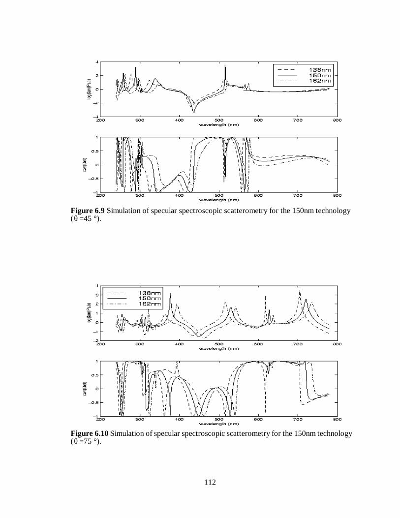
112
Figure 6.9 Simulation of specular spectroscopic scatterometry for the 150nm technology ( =45 °).θ
Figure 6.10 Simulation of specular spectroscopic scatterometry for the 150nm technology ( =75 °).θ

113
Figure 6.11 Simulation of specular spectroscopic scatterometry for the 100nm technology ( =45 °).θ
Figure 6.12 Simulation of specular spectroscopic scatterometry for the 100nm technology ( =75 °).θ

114
6.3 A Library-Based Methodology for CD Profile Extraction
The extraction of a CD profile can be viewed as an optimization problem. The objective is
to find a profile whose simulated diffraction responses match the measured responses.
Optimization techniques, such as simulated annealing and gradient based optimization
techniques, can be applied. However, for complicated profiles, it is computationally pro-
hibitive to exhaustively search for the optimal profiles. A practical way is to generate the
simulation responses before the measurement. A library-based methodology for CD profile
extraction is proposed in this work.
Figure 6.13 describes the extraction flow.
• First, mask information, technology characteristics, thin-film information (optical
properties , and thickness values), are used to obtain a collection of profiles. The
profile information includes the information of the grating layer and all the underneath
layers. The profiles can be obtained by a tuned TCAD simulator, or by a random profile
generator. The collection of profiles should be sufficient and efficient. Sufficient means
measured
gtk
Figure 6.13 A library based methodology for CD profile extraction.
profile
responseSimulatedDiffraction
GratingResponseLibrary
extracted profiles
n k

115
that there should be enough profiles in the library for most possible process results,
while efficient means that there should not be too many unnecessary profiles in the
library.
• Second, the profiles are used as inputs to a diffraction grating simulator, such as gtk, to
generate the simulated diffraction responses. Usually the diffraction efficiencies,
and are simulated over a wide range of wavelengths.
• For in-situ specular spectroscopic scatterometry use, the diffraction responses are mea-
sured and compared with the library. When the library is complete, there will be one or
more profiles whose simulated responses match those of the measured sample.
The key of the success for this library-based extraction methodology is the completeness
of the library combined with efficient search methods.
The uniqueness of solution is an issue in this approach. In other words, it is possible that
different profiles may lead to similar diffraction responses. There are several theoretical
works on this issue [6.14][6.15]. In this thesis, the problem will be addressed experimen-
tally.
6.4 Experimental Verification
The experimental verification of specular spectroscopic scatterometry consists of two
parts: the verification of the forward diffraction grating simulation from given CD profiles
and the verification of the inverse CD profile extraction from the scatterometry measure-
ment.
In this section, we consider a focus-exposure matrix experiment. As shown in Figure 6.14,
we have 5 focus settings and 7 dose settings. The dose settings are coded as -3, -2, -1, 0, 1,
2, and 3, indicating the values from 11.5 mJ/cm2 to 14.5 mJ/cm2 in steps of 0.5 mJ/cm2.
The focus settings are coded as -2, -1, 0, 1, and 2, indicating the values from -0.2 µm to 0.2
µm in steps of 0.1µm. In total we have 31 settings on each wafer. The mask has 0.28µm/
0.28µm line/space gratings. The thin-film stack includes DUV photoresist Shipley UV5TM,
a bottom anti-reflection coating and a silicon substrate. After exposure and PEB, UV5 was
developed to form 200µm-by-200µm grating regions. A KLA-Tencor Prometrix® UV-
Ψtan
∆cos

116
1280SE was used to measure the ratio of 0th order TE and TM fields. The incident angle is
70.5 °. The light beam was focused on a 30µm-by-70µm region.
Figure 6.15 and Figure 6.16 show the measured and on each die in the whole
wafer. Figure 6.17 plots the detailed information of the dose effect on the signal with
a fixed focus. Different dose and focus values generate different CD grating profiles, thus
different 0th order diffraction responses. It is interesting to notice that different grating pro-
UV5
BARC
SI
0.28µm 0.28µm
Figure 6.14 (a) Grating structures; (b) Focus-exposure matrix experiment setup for experimental verification.
dose(mJ/cm2)
focu
s(µm
)
11.5 12.0 13.0 13.5 14.0 14.5-0.2
-0.1
0
0.1
0.2
-3 -2 -1 0 1 2 3
-2
-1
0
1
2
12.5
(a)
(b)
Ψtan ∆cos
Ψtan

117
files generate significantly different , even at higher wavelengths (compared to the
CD linewidth). The same behavior is also observed for from Figure 6.18.
Ψtan
∆cos
Figure 6.15 of the entire F-E matrix.Ψtan
-3 -2 -1 0 1 2 3
-2
-1
0
1
2
Figure 6.16 of the entire F-E matrix.∆cos
-3 -2 -1 0 1 2 3
-2
-1
0
1
2

118
Figure 6.17 of the fixed focus (-1) level and different dose levels (from -3 to +3).Ψtan
-3
+3
Figure 6.18 of the fixed focus (-1) level and different dose levels (from -3 to +3).∆cos
-3
+3

119
To verify the forward diffraction grating simulation, we use AFM to measure several struc-
tures from the dose-focus matrix. Figure 6.19 is the calibrated CD profile of dose level -1
and focus level -1. To approximate this complicated profile, the photoresist is sliced into
100 layers. The optical properties of photoresist are shown in Figure 6.6, and the optical
properties of ARC are shown in Figure 6.20. The thickness of ARC is 162.9nm. There are
31 TE and 41 TM orders retained in the RCWA simulation. The diffracted fields are calcu-
lated from 240nm to 800nm with 1nm wavelength resolution. Figure 6.21 and Figure 6.22
show the measured and simulated and from this grating profile. Figure 6.23
and Figure 6.24 show the residual plots from the measured and simulated and ,
respectively. We can see that the simulated and measured diffracted fields match very well.
Ψtan ∆cos
Ψtan ∆cos
Figure 6.19 Calibrated CD AFM profile of the dose level -1 and focus level -1.

120
Figure 6.20 The optical properties of the ARC in the experiment.
n k
Figure 6.21 Measured and simulated tanΨ from the AFM CD profile.

121
Figure 6.22 Measured and simulated cos∆ from the AFM CD profile.
Figure 6.23 Residual plot of the measured and simulated tanΨ from the AFM CD profile.

122
The library-based CD profile extraction methodology described in section 6.3 is imple-
mented. A profile library is randomly generated from a set of profile primitives. Shown in
Figure 6.25, a profile consists of three parts, the top, the middle and the bottom. We have
about 30 pre-defined “shapes” for these three parts. These pre-defined “shapes” are also
called profile primitives. To generate a profile, we randomly select a primitive for top,
middle and bottom. Each primitive is further scaled by two random scaling parameters to
control the width and thickness. The ARC thickness is also randomly generated to accom-
modate the process variation.
There are 19 total layers for the photoresist. We assign 10 layers to the top part, 7 layers to
the middle part and 2 layers to the bottom part. The thickness of each layer needs not to be
the same.
Figure 6.24 Residual plot of the measured and simulated cos∆ from the AFM CD profile.

123
About 180,000 profiles are generated, and the corresponding diffraction responses are sim-
ulated by gtk. Because of the computational cost, each grating profile is simulated every
10nm from 240nm to 780nm. The number of retained orders for TE and TM are 31 and 41,
respectively. Using gtk, the simulation for one profile, which includes both TE and TM on
53 wavelengths, takes approximately 2 minutes on a Sun UltraSparc I 167MHz worksta-
tion.
To extract the CD profile from a measurement, the measured and are com-
pared with each simulated and in the library. If there is a “good” match
between the measured and simulated signals, the corresponding CD profile is considered
as the extracted profile. Mathematically, the matching is by minimizing the cost function
(6.1)
Figure 6.25 Random CD profile library generation.
top
middle
bottom
Ψtan ∆cos
Ψtan ∆cos
min Ψ measured λ,tan( )log Ψ theoretical λ,tan( )log–( )2w Ψtan λ,
∆measured λ,cos ∆theoretical λ,cos–( )2w ∆cos λ,
+(
)
λ∑

124
by searching the library. In this case we set . As discussed in
Chapter 4, we use a logarithm transformation on to stabilize the signal.
For example, for the focus-exposure matrix shown in Figure 6.14, given the and
signal at focus level -1 and exposure level -1, we found several close “matches”. We
did not just choose the closest match because we want to examine the uniqueness problem.
Figure 6.26 and Figure 6.27 show the matched simulated and measured signals. Figure 6.28
compares the extracted profiles to the AFM measurement. There are two observations.
First, the AFM measurement agrees with those extracted profiles; second, similar diffrac-
tion responses also have similar grating profiles. Figure 6.29 shows the comparison
between the extracted profiles and AFM measurements across the entire focus-exposure
matrix.
w Ψtan λ, w ∆cos λ, 1= =
Ψtan
Ψtan
∆cos
Figure 6.26 Matching on the simulated and measured tanΨ signal.
simulatedmeasured
family of

125
Figure 6.27 Matching on the simulated and measured cos∆ signal.
simulated
measured
family of
Figure 6.28 Comparison between the extracted CD profiles and the CD-AFM profile.

126
6.5 Conclusions
With the progress of deep sub-micron technology, the accuracy and efficient measurement
of parameters such as the line width, height/depth and side-wall profile are becoming
increasingly critical to develop and characterize lithography and plasma etch processes. In
this chapter, specular spectroscopic scatterometry is introduced for in-situ DUV lithogra-
phy, which includes using RCWA to simulate the electromagnetic response of gratings
with different profiles, and using spectroscopic ellipsometry to measure 1D gratings. A
library-based methodology for profile extraction is proposed and implemented. A focus-
exposure matrix experiment is used for the verification. This metrology can be used with
current technology, and it is expected to be able to extend to the 0.1µm generation. The sig-
Figure 6.29 Comparison between the extracted grating profiles and the CD-AFM profiles across the focus-exposure matrix. The four AFM profiles with (dose, focus) level of (2,-2), (3,-1), (-1,2) and (2,2) have not been measured.
-3 -2 -1 0 1 2 3
-2
-1
0
1
2

127
nificance of this work is that we shift the complexity of metrology from specialized hard-
ware, such as CD-SEMs, to sophisticated data analysis in conjunction with existing
equipment, such as spectroscopic ellipsometers.

128
References for Chapter 6
[6.1] “The National Technology Roadmap for Semiconductors Technology Needs”,1997 Edition, Semiconductor Industry Association (SIA).
[6.2] H. P. Kleinknecht and H. Meier, “Linewidth measurement on IC masks andwafters by grating test patterns”, Applied Optics, vol. 19, 525-533, 1980.
[6.3] W. A. Bosenberg and H. P. Kleinknecht, “Linewidth measurement on IC wafersby diffraction from grating test patterns”, Solid State Technology, vol. 26, 79-85,July 1983.
[6.4] H. S. Damar, E. P. Chan, T. T. Wu, A. R. Neureuther, “Diffraction characteriza-tion for process monitoring, linewidth measurement and alignment”, Proc. ofSPIE, vol. 470, 157-163, 1984.
[6.5] D. Nyyssonen and C. P. Kirk, “Optical microscope imaging of lines patterned inthick layers with variable edge geometry: theory”, J. Opt. Soc. Am. A, vol.5, no.8,1270-1280, Aug. 1988.
[6.6] C. Yuan and A. J. Strojwas, “Modeling optical equipment for wafer alignment andline-width measurement”, IEEE Trans. on Semiconductor Manufacturing, vol.4,no.2, 99-110, May 1991.
[6.7] K. Tadros, A. R. Neureuther and R. Guerrieri, “Understanding metrology of poly-silicon gates through reflectance measurements and simulation”, Proc. of SPIE,vol.1464, 177-186, 1991.
[6.8] T. A. Brunner, A. L. Martin, R. M. Martino, C. P. Ausschnitt and T. Newmann,“Quantitative stepper metrology using the focus monitor test mask”, Proc. of SPIE,vol. 2197, 541-549, 1994.
[6.9] N. Jakatdar, X. Niu, C. J. Spanos, A. Romano, J. Bendik, and R. Kovacs, “Charac-terization of a positive chemically amplified photoresist for process control”, Proc.of SPIE, vol. 3332, 586-593, 1998.
[6.10] T. Koizumi, T. Matsuo, M. Endo and M. Sasago, “CD control using latent imagefor lithography”, Proc. of SPIE, vol. 2439, 418-26, 1995.

129
[6.11] D. Ziger, T. Adams and J. Garofalo, “Linesize effects on ultraviolet reflectancespectra”, Optical Engineering, vol. 36, no.1, 243-250, Jan. 1997.
[6.12] C. Raymond, M. Murnane, S. Prins, S. S. H. Naqvi, et; al, “Multiparameter gratingmetrology using optical scatterometry”, J. Vac. Sci. Tech. B, vol. 15, no.2, 361-368, 1997.
[6.13] S. Bushman and S. Farrer, “Scatterometry measurements for process monitoring ofpolysilicon gate etch”, Proc. of SPIE, vol. 3213, 79-90, 1997.
[6.14] A. Roger and M. Breidne, “Grating profile reconstruction by an inverse scatteringmethod”, Optics Communications, vol. 35, no. 3, 299-302, 1980.
[6.15] G. Bao, “On the relation between the coefficients and solutions for a diffractionproblem”, Inverse Problems, vol. 14, no. 4, 787-798, Aug. 1998.
[6.16] X. Niu, N. Jakatdar, J. Bao and C. J. Spanos, “Specular Spectroscopic Scatterome-try in DUV Lithography”, SRC Techcon’98.

130
Chapter 7Conclusion and Future Work
7.1 Thesis Summary
The history of semiconductor industry has been characterized by Moore’s Law. Moore’s
Law predicts the exponential scaling factor for integrated circuit density. However, this
aggressive scaling is linked to a dramatic increase of the cost for equipment. Affordable
lithography and metrology at and below 100nm now become the grand challenges.
This thesis has presented a systematic metrology approach for unpatterned and patterned
wafers in the lithography process. For unpatterned wafers, the most important observables
are the thickness and optical properties, and , of the layers. For patterned wafers, the
most important observables are the profiles of the critical features.
Sophisticated dispersion models derived from the Kramers-Kronig relations are used with
a powerful global optimizer for unpatterned thin-film characterization. Several algorithms
of simulated annealing for continuous variables are reviewed and discussed in Chapter 3.
In Chapter 4, the metrology by solid (polysilicon) and polymer (photoresist) thin-film char-
acterization is demonstrated. A statistical enhancement strategy is proposed, based on com-
puter experiments and a Bayesian variable screening technique to overcome the large
metrology dimension problem. A bootstrap method is introduced for testing the accuracy
of simulated annealing.
For patterned thin-film metrology, we introduce the concept of specular spectroscopic scat-
terometry. Scatterometry is one of the few metrology candidates that has true in-situ poten-
tial for deep sub-micron CD and profile analysis. The ability to simulate the behavior of
diffraction gratings with high precision is the key to the success of specular spectroscopic
n k

131
scatterometry. Chapter 5 is devoted to the numerically rigorous analysis on diffraction grat-
ings. The Grating Tool-kit (gtk) is implemented for one-dimensional grating analysis. It is
shown that the choice of an efficient formulation with an appropriate number of retained
orders in RCWA are very important considerations for balancing simulation accuracy and
speed. Chapter 6 illustrates the concept and design of specular spectroscopic scatterometry.
A library-based CD profile extraction methodology is introduced and validated with a
focus-exposure matrix experiment.
7.2 Future Work
The theme of this thesis is that, through the aid of computation and intelligent data analysis
techniques, more process information can be extracted from existing sensors. This infor-
mation can be used for process improvement through control, in this way, the equipment
cost can be shifted to computation. For a long time, it has been very difficult to apply con-
trol to the entire lithography sequence, because of the time and cost involved in CD metrol-
ogy. Part of the problem was that the linewidth value alone is not adequate to characterize
the lithography process. With the assistance of specular spectroscopic scatterometry, it is
expected that control of the entire lithography sequence can become realistic. At the same
time, the use of profile information for process control becomes an interesting research
topic.
Although the methods developed in this study are targeting lithography, the methodology
presented is general and can be applied to other process steps. For example, knowledge of
the CD profiles in the plasma etching process is also important, specular spectroscopic scat-
terometry can be transferred easily to the etching process.
Modern microprocessor chips consist of up to twenty million transistors fabricated on a
single die. To interconnect this large number of devices, typical chips include four to six
conductor levels with high density wiring, having sub-micron widths and spacings. Char-
acterization for interconnect is essential. Metal has a finite conductivity in the visible
region. Preliminary study shows that specular spectroscopic scatterometry can be used for
metallic gratings when there is a non-metallic substrate. It is expected that specular spec-

132
troscopic scatterometry can be used for interconnect profile extraction and mask inspection
as well.

133
Appendix ASymbols Used in Chapter 5
The wavelength of incident light.
The permittivity in free space.
The permeability in free space.
The wave number.
The total number of the layers the grating system has.
The angle of the incident light to the grating normal in the plane
of incidence.
The azimuthal angle of the plane of incidence.
The angle between the electric-field vector and the plane of incidence.
The wavelength of the incident light.
The grating period.
The complex refractive index of th layer.
The orders retained of the space harmonics in the coupled wave field
expansion are , , , 0, , , .
The permittivity of the th layer.
The th order permittivity of the th layer in the 1-D coupled wave
analysis.
λ
ε0
µ0
k
L
θ
φ
ψ
λ
D
ni i
o
o– o 1–( )– … … o 1–( ) o
εl l
εl h, h l

134
The Toeplitz matrix formed by the permittivity harmonic components in the
th layer.
The inverse permittivity of the th layer.
The th order inverse permittivity of the th layer in the 1-D coupled wave
analysis.
The Toeplitz matrix formed by the inverse permittivity harmonic
components in the th layer.
The Kronecker symbol.
The electric field.
The magnetic field.
The normalized amplitude of the electric field.
The normalized amplitude of the magnetic field.
The index of diffracted wave.
The diffraction efficiency.
The space-dependent part of the wave function.
The angular frequency.
The phase velocity of a wave.
The unit vector of a periodic medium.
The basis vector of a reciprocal lattice.
El
l
πl l
πl h, h l
Pl
l
δ
E
H
S
U
m
DE
ζ
ω
V r( )
d
b

135
Appendix Bgtk
This appendix contains the information on how to use gtksh, the Tcl interface for the Grat-
ing ToolKit (gtk). Tcl is a scripting language designed and crafted by Prof. John Ousterhout
of University of California, Berkeley [B.1].
B.1 The gtksh Command Syntax
Table B.1. 1D grating commands
Grating1D grating create a grating object instance “grating”
grating setL L set the layer number
grating setTheta thetagrating setPsi psigrating setPhi phi
set the incident angles (unit in degree)
grating setD D set the grating period (unit in nm)
grating addLayer layerIndex width thickness N
add a layer in the “layerIndex” layer. The width is in nm and thickness is also in nm. N is the name of the variable of refractive index. For the semi-infinite layers, set the width be the grating period and thickness be -1.

136
B.2 An Example
In this example, there are two materials involved in the grating. The structure of the grating
is illustrated in Figure B.1. The optical properties are , , the
grating period is 1 µm, the duty cycle is 0.5, the wavelength λ = 1µm, θ= 30 °. The total
reflected intensity is studied as a function of the number of retained orders for grating thick-
ness of 0.01λ, 0.05λ, 0.5λ. These grating cases are taken from Lalanne’s paper [B.2].
grating FTE ordergrating FTM1 ordergrating FTM2 ordergrating FCon1 ordergrating FCon2 order
calculate the diffraction efficiency of the grating object with the number of specified retained order. 2*(2*order+1) values are returned. The first half is for the reflected efficiencies and the second half is for the transmitted efficiencies. The sequence of the order is in [-order, -(order-1), ..., 0, ..., (order-1), order]
set n 1000 1 0 The refractive index are 3-component list. The first component is the wavelength (unit in nm), the second part is the and the third part is .
Table B.1. 1D grating commands
n k
n0 1= n1 3.18 j4.41–=
0
1
2
Figure B.1 A grating structure.

137
proc first_half_sum x set y 0 set length [llength $x] set first_half [lrange $x 0 [expr $length / 2 - 1]] foreach i $first_half set y [expr $y + $i] return $y
# Construct the refractive index.set n0 1000 1 0set n1 1000 3.18 -4.41
# Construct the grating objectGrating1D gratinggrating setL 2grating setTheta 30.0grating setD 1000grating addLayer 0 1000 -1 n0grating addLayer 1 500 [expr 0.01 * 1000] n1grating addLayer 2 1000 -1 n1
# 0.01 lambdafor set i 0 $i < 30 incr i set str "[expr $i * 2 + 1] \t [first_half_sum [grating FTM1 $i]] \t [first_half_sum [grating FTM2 $i]]" puts $str
Figure B.2 A Tcl code sample.
T = 0.01 λ
Figure B.2 Computation result shows the effect of a grating structure on the convergence rate.
T = 0.05 λ T = 0.5 λ

138
B.3 Reference
[B.1] John Ousterhout, “Tcl and Tk Toolkit”, Addison-Wesley, 1994.
[B.2] P. Lalanne, “Convergence performance of the coupled-wave and the differentialmethods for thin gratings”, J. Opt. Soc. Am. A, July 1997.

139
Appendix CThe TEMPEST Script Used in Section 5.8
/*tmpstTE.inCreated by Tom Pistor.*/
wavelength .248max_cycle 200x_node 80y_node 1z_node 320x_dim .56order_source node 290 -1 te 0 0 1000 0rectangle node 0 79 0 0 0 159 index 1 0rectangle node 0 79 0 0 0 79 dispersive 1.6591 3.5227rectangle node 0 79 0 0 80 100 index 1.695 .560rectangle node 0 39 0 0 101 208 index 1.85 .022rectangle node 0 79 0 0 0 0 black_matterrectangle node 0 79 0 0 312 319 pml 0 0 1 1 1 0 0
plot block node 0 79 0 0 0 319 tmpstTE.blkplot ex steady 0.00 node 0 79 0 0 0 319 tmpstTE.e.x.iplot ey steady 0.00 node 0 79 0 0 0 319 tmpstTE.e.y.iplot ez steady 0.00 node 0 79 0 0 0 319 tmpstTE.e.z.iplot ex steady 0.25 node 0 79 0 0 0 319 tmpstTE.e.x.qplot ey steady 0.25 node 0 79 0 0 0 319 tmpstTE.e.y.qplot ez steady 0.25 node 0 79 0 0 0 319 tmpstTE.e.z.q


![OPTICAL COHERENCE TOMOGRAPHY FOR DIMENSIONAL METROLOGY … · Optical coherence tomography (OCT), a technology commonly used to image sub-surface structures in vivo [3], is based](https://static.fdocuments.in/doc/165x107/5f0490e47e708231d40e9a4a/optical-coherence-tomography-for-dimensional-metrology-optical-coherence-tomography.jpg)