
An Integrated Power Supply System for Low Power
9
IEEE JOURNAL OF SOLID-ST A TE CIRCUITS, VOL. 45, NO. 1, J ANUARY 2010 205 An Integrated Power Supply System for Low Power 3.3 V Electronics Using On-Chip Polymer Electrolyte Membrane (PEM) Fuel Cells Mirko Frank, Matthias Kuhl, Gilbert Erdler, Ingo Freund, Yiannos Manoli, Claas Müller, and Holger Reinecke Abstract—A stab ilize d powe r suppl y r eali zed by chip- integ rate d micro fuel cells within an extended CMOS process is presented in this paper. The fuel cell system delivers a maximum power output of 450 μW/cm 2 . The electr onic contro l cir cuit ry consists of an LDO, an on-chip oscillator and a programmable timing network. The core system consu mes an av erag e powe r of 620 nW. The system reaches a current efficiency of up to 92% and provides a constant output voltage of 3.3 V. Index Terms—CMOS comp atib le chip- integ rated micr o fuel cell , electronic control circuit, integrated metal hydrogen storage, sta- bilized on-chip power supply. I. INTRODUCTION R ECENT advances in miniaturization of both electronics and MEMS de vic es ha ve res ulted in a con sid era ble po wer reduction [1]. On the other hand, the size of power supplies for such miniaturized devices has scaled down only marginally. Downsizing conventional batteries to wafer level causes various pro ble ms. For example ele ctr odematerials or liq uid ele ctr oly tes of the chi p-i nte gra ted bat ter ies jus t as those of conve nti onal sys - tems have to be hermetically sealed in order to prevent defects caused by interaction with oxygen or water in ambient atmos- phere. The system presented in this paper consists of fuel cells (FCs) connected in series, so called fuel cell cascades (FCCs) (Fig. 1), a core system to control the output voltage by a low dropout voltage regulator (LDO) (Fig. 2) and circuitry to check and byp ass empty or defectiv e FCs to kee p the FCCs fu nctio nal. The paper is organized as follows. Section II describes the principle setup and functionality of the integrated fuel cell cas- cades. In Section III the working principle of the electrical com- ponents and their interaction with the integrated fuel cells is ex- plained. Section IV describes the extended CMOS fabrication process of the integrated fuel cells. The experimental results are dis cus sed in Sec tio n V and the pap er clo ses wit h the con clu sio ns in Section VI. Manuscript received May 15, 2009; revised July 22, 2009. Current version published December 23, 2009. This paper was approved by Guest Editor Kevin Zhang. M. Frank, M. Kuhl, Y. Manoli, C. Müller, and H. Reinecke are with the Department of Microsystems Engineering (IMTEK), University of Freiburg, D-79110 Freiburg, Germany (e-mail: mfrank@imtek .de). G. Erdler and I. Freund are with Micronas GmbH, D-79108 Freiburg, Ger- many. Color versions of one or more of the figures in this paper are available online at http://ieeexplo re.ieee.org. Digital Object Identifier 10.1109/JSSC.2009.2034441 Fig. 1. Proto type of the fuel cell cascade s, 7 casca des consi sting of 8 single chip-integrated fuel cells in a PLCC68 ceramic package. II. INTEGRATED FUEL CELLS A. Setup of a Single Int eg rated Fuel Cell Conventional PEM fuel cells consist of a polymer electrolyte membrane (PEM), two gas diffusion electrodes, two diffusion layers and two flow fields. The reactants e.g., hydrogen and oxygen are supplied to the gas diffusion electrodes over feed pipes out of external tanks. The amount of supplied fuel is often con tro lled by act ive sys tem per iph ery lik e pre ssu re red uce rs and valves. For the chip integration a new setup principle of PEM fuel cells was developed [2], the new kind of fuel cell is made up of a palladium based hydrogen storage and an air breathing cathode both separated by a PEM. The layout of an integrated fuel cell is depicted in Fig. 3. Advantages of the new approach are the omission of active devices for fuel supply and the reduc- tion of system components like flow fields and diffusion layers. Due to the simple assembly process, the fuel cells can be pro- duced by thin film technologies and can be fabricated within an extended CMOS process. B. The Integr ated Hydr ogen Stora ge Palladium is used for the storage of hydrogen. This metal is known for its extraordinary ability to store huge amounts of hy- drogen. At room temperature and atmospheric pressure palla- dium can store about 900 times as much hydrogen as its own volume, which corresponds to an atomic relation of hydrogen to palladium (H/Pd) of at least 70% (Fig. 4). The theoretical ca- pa ci ty of pa ll adium is ca lc ul at ed to 2. 12 Ah/c m , which is in the 0018-9200/$26.00 © 2009 IEEE Authorized licensed use limited to: K.S. Institute of Technology. Downloaded on January 31, 2010 at 03:54 from IEEE Xplore. Restrictions apply.
-
Upload
bharath-s-l-bharath -
Category
Documents
-
view
221 -
download
0
Transcript of An Integrated Power Supply System for Low Power

8/7/2019 An Integrated Power Supply System for Low Power
http://slidepdf.com/reader/full/an-integrated-power-supply-system-for-low-power 1/9
IEEE JOURNAL OF SOLID-STATE CIRCUITS, VOL. 45, NO. 1, JANUARY 2010 205
An Integrated Power Supply System for Low Power3.3 V Electronics Using On-Chip Polymer Electrolyte
Membrane (PEM) Fuel CellsMirko Frank, Matthias Kuhl, Gilbert Erdler, Ingo Freund, Yiannos Manoli, Claas Müller, and Holger Reinecke
Abstract—A stabilized power supply realized by chip-integratedmicro fuel cells within an extended CMOS process is presented inthis paper. The fuel cell system delivers a maximum power outputof 450 μW/cm
2
. The electronic control circuitry consists of anLDO, an on-chip oscillator and a programmable timing network.The core system consumes an average power of 620 nW. Thesystem reaches a current efficiency of up to 92% and provides aconstant output voltage of 3.3 V.
IndexTerms—CMOS compatible chip-integrated micro fuel cell,electronic control circuit, integrated metal hydrogen storage, sta-bilized on-chip power supply.
I. INTRODUCTION
RECENT advances in miniaturization of both electronics
and MEMS devices have resulted in a considerable power
reduction [1]. On the other hand, the size of power supplies
for such miniaturized devices has scaled down only marginally.
Downsizing conventional batteries to wafer level causes various
problems. For example electrode materials or liquid electrolytes
of the chip-integrated batteries just as those of conventional sys-
tems have to be hermetically sealed in order to prevent defectscaused by interaction with oxygen or water in ambient atmos-
phere. The system presented in this paper consists of fuel cells
(FCs) connected in series, so called fuel cell cascades (FCCs)
(Fig. 1), a core system to control the output voltage by a low
dropout voltage regulator (LDO) (Fig. 2) and circuitry to check
and bypass empty or defective FCs to keep the FCCs functional.
The paper is organized as follows. Section II describes the
principle setup and functionality of the integrated fuel cell cas-
cades. In Section III the working principle of the electrical com-
ponents and their interaction with the integrated fuel cells is ex-
plained. Section IV describes the extended CMOS fabrication
process of the integrated fuel cells. The experimental results arediscussed in Section V and the paper closes with the conclusions
in Section VI.
Manuscript received May 15, 2009; revised July 22, 2009. Current versionpublished December 23, 2009. This paper was approved by Guest Editor KevinZhang.
M. Frank, M. Kuhl, Y. Manoli, C. Müller, and H. Reinecke are with theDepartment of Microsystems Engineering (IMTEK), University of Freiburg,D-79110 Freiburg, Germany (e-mail: [email protected]).
G. Erdler and I. Freund are with Micronas GmbH, D-79108 Freiburg, Ger-many.
Color versions of one or more of the figures in this paper are available onlineat http://ieeexplore.ieee.org.
Digital Object Identifier 10.1109/JSSC.2009.2034441
Fig. 1. Prototype of the fuel cell cascades, 7 cascades consisting of 8 singlechip-integrated fuel cells in a PLCC68 ceramic package.
II. INTEGRATED FUEL CELLS
A. Setup of a Single Integrated Fuel Cell
Conventional PEM fuel cells consist of a polymer electrolyte
membrane (PEM), two gas diffusion electrodes, two diffusion
layers and two flow fields. The reactants e.g., hydrogen and
oxygen are supplied to the gas diffusion electrodes over feed
pipes out of external tanks. The amount of supplied fuel is often
controlled by active system periphery like pressure reducers and
valves. For the chip integration a new setup principle of PEM
fuel cells was developed [2], the new kind of fuel cell is made
up of a palladium based hydrogen storage and an air breathing
cathode both separated by a PEM. The layout of an integrated
fuel cell is depicted in Fig. 3. Advantages of the new approach
are the omission of active devices for fuel supply and the reduc-
tion of system components like flow fields and diffusion layers.Due to the simple assembly process, the fuel cells can be pro-
duced by thin film technologies and can be fabricated within an
extended CMOS process.
B. The Integrated Hydrogen Storage
Palladium is used for the storage of hydrogen. This metal is
known for its extraordinary ability to store huge amounts of hy-
drogen. At room temperature and atmospheric pressure palla-
dium can store about 900 times as much hydrogen as its own
volume, which corresponds to an atomic relation of hydrogen
to palladium (H/Pd) of at least 70% (Fig. 4). The theoretical ca-
pacity of palladium is calculated to 2.12 Ah/cm , which is in the
0018-9200/$26.00 © 2009 IEEE
Authorized licensed use limited to: K.S. Institute of Technology. Downloaded on January 31, 2010 at 03:54 from IEEE Xplore. Restrictions apply.

8/7/2019 An Integrated Power Supply System for Low Power
http://slidepdf.com/reader/full/an-integrated-power-supply-system-for-low-power 2/9
206 IEEE JOURNAL OF SOLID-STATE CIRCUITS, VOL. 45, NO. 1, JANUARY 2010
Fig. 2. Chip photo after CMOS fabrication depicting the core system.
Fig. 3. Layout of a chip-integrated fuel cell andits performance data comparedto state of the art wafer level batteries (WLB).
same range as Lithium (2.09 Ah/cm ). Calculating the theoret-
ical capacity of the chip integrated fuel cell, the thicknesses of
all the active fuel cell components have to be considered. In the
actual assembly the hydrogen storage represents approximately
1/4 of the total volume of the micro energy device, the capacity
of the chip integrated fuel cell results in Ah cm
mAh cm . Therefore, the fuel cell has the potential to pro-
vide higher capacity than state-of-the-art wafer level batteries
(WLB) based on lithium-ion technology (Fig. 3) [4]. Since theoptimization of the system components is still in progress, a
comprehensive characterization of the chip-integrated fuel cell
system could not yet be completed. The values for energy den-
sity are based on the considerations made above; power density
results were gained by the characterization of the hybrid system
given in Section V-A. Data about shelf life of the micro en-
ergy system are based on the characterization of single chip-in-
tegrated fuel cells. These measurements revealed open circuit
voltage values above 500 mV for more than 100 days.
Advantages of palladium compared to lithium based cells are
its non toxicity and the fact that it is inert to environmental
gases like oxygen or nitrogen. Thus, the integrated, thick sealing
layer which prevents the intrusion of gases and humidity inlithium-based wafer level batteries can be omitted. The metal
Fig. 4. Pressure-Isotherm of the Palladium-hydrogen system [3].
palladium is already being used in CMOS compatible semi-
conductor processes like the fabrication of hydrogen sensors
and the backside conduction of silicon wafers [5], [6]. When a
palladium layer is evaporated onto a silicon chip, directly con-
nected to the circuitry and loaded with hydrogen, a storage with
high capacity, fully integrated onto a chip, can be realized. The
amount of stored hydrogen and therefore the fuel cell’s capacity
of electrical energy can be controlled by the thickness of the
palladium layer. Thin films can be fabricated by evaporation
onto silicon substrates; thicker films up to some 100 μm can be
fabricated by electroplating of palladium or by thick film tech-
niques like screen printing. Despite the unique scalability of the
thickness of the fuel cell’s hydrogen storage up to some hun-
dred micrometers, the power and energy density of wafer level
batteries, as reported in [7], [8], cannot be compared to con-
ventional macroscopic systems since the volume fraction of thepassive components (electrodes, substrate and sealing) becomes
very dominant compared to the volume of the active storage ma-
terials. Thus, the achievable maximum energy density in micro-
scopic systems is significantly smaller than that of conventional
systems.
C. Working Principle of the Integrated Fuel Cell
When operating the fuel cell, the hydrogen atoms stored
within the palladium storage are split up into protons and elec-
trons. The electrons are conducted through the external circuit
to the cathode of the fuel cell driving the load. The protons are
transported to the cathode by proton hopping through the protonconductive PEM. At the cathode the electrons, the protons and
oxygen—which is supplied by the ambient air—catalytically
recombine to water. The integrated fuel cells do not need
complex sealing layers. In the cathode of the system no reactive
electrode material has to be stored, since ambient oxygen is
used.
D. The Fuel Cell Cascades
Within its operation range, each single fuel cell delivers a
characteristic output voltage between 500 mV and 800 mV.
The layout of the integrated fuel cells brings the contacts of the
anode and the cathode back to the silicon substrate. This fact al-lows the connection of several fuel cells in series or in parallel,
Authorized licensed use limited to: K.S. Institute of Technology. Downloaded on January 31, 2010 at 03:54 from IEEE Xplore. Restrictions apply.

8/7/2019 An Integrated Power Supply System for Low Power
http://slidepdf.com/reader/full/an-integrated-power-supply-system-for-low-power 3/9
FRANK et al.: AN INTEGRATED POWER SUPPLY SYSTEM FOR LOW POWER 3.3 V ELECTRONICS 207
Fig. 5. Schematic of the integrated power supply and FC control system. Thecircuit is supplied by V (1 V–1.5 V).
so the desired output voltage can be adjusted by the number of
connected fuel cells.
The currently developed process enables the integration of
intelligent energy sources with CMOS circuitry. Another unique
aspect of this technology is the possibility to adapt the capacity
and the power density of the cells independent of each other.
The capacity is adapted by the volume of the hydrogen storage,
the power output by the area of the fuel cells and the outputvoltage by the number of connected fuel cells in series within a
cascade. By integrating several fuel cell cascades onto a silicon
chip a highly reliable power supply for autonomous systems can
be realized.
III. INTEGRATED ELECTRONICS
A. System Approach
The underlying 0.45 μm CMOS process enables an inte-
grated wake up and power supply system directly connected
to the FCCs. Thereby the FCs can be combined with an en-ergy management without the need of external components or
user intervention. The proposed electronic control circuitry is
designed to optimize the lifetime of e.g., autonomous sensor
systems (Fig. 5). Therefore, a periodic system wake-up is
implemented, controlled by an on-chip oscillator and a pro-
grammable timing network. To generate a constant output
voltage of 3.3 V for duty-cycled measurement tasks, the FCCs
are activated after each single cell is checked for functionality
and shorted by a bypass if found faulty. After check-up com-
pletion, an LDO is switched on to power the load during one
measurement event.
As presented in Section II-D several fuel cells can be stacked
to increase the output voltage. The presented realization uses7 fuel cells per cascade for an open circuit voltage of 6.3 V.
Fig. 6. Schematic of the 620 nW 33.3 kHz current starved ring oscillator.
To increase the system’s maximum output current 6 fuel cellcascades have been implemented in parallel.
B. Core System
For the benefit of the system’s lifetime, the core system is
restricted to fundamental control elements like an oscillator and
an asynchronous timing network to avoid current peaks. It is
powered by a redundant 2-FC-stack generating 1 V to 1.5 V
depending on the charging level of the fuel cells.
The implemented low power oscillator is realized as a cur-
rent starved inverter chain with 9 stages to (Fig. 6) [9].
To cancel out the simulated frequency drift with temperature of
208 Hz/K, the oscillator is supplied by a complementary-to-ab-solute-temperature (CTAT) current source. Due to the current
starved architecture a very constant system cycle time without
the need of external components can be realized.
The current source feeding the current starved oscillator
(Fig. 6) delivers a voltage of around 0.74 V at the 10
inverter stages. Thus, a buffer is required to shift the output
level to by up to a factor of 2. To minimize the current
consumption, no classical level shifter is used but the first
output buffer stage is cascaded with an nMOS transistor driven
by , to prevent dynamical current losses caused by the slow
rising edge of this stage. The D-FF guarantees a duty cycle of
50%. The connected timer realized as a D-FF frequency dividerchain provides system cycle times adjustable between 30 ms
and 4 years.
The asynchronous realization relaxes the dynamic perfor-
mance requirements of the small fuel cells supplying the core
system. The current consumption spreads over time and there
are no current peaks as would be present in the case of a
synchronous design. As soon as the externally programmable
system cycle time is elapsed, all fuel cell cascades are tested
in parallel from bottom to top. After the check is completed
and if not more than 3 cells within one FCC are damaged, this
cascade is handled as “usable”. When at least 3 FCCs have
reached this status, the LDO is powered up by all functional
fuel cell cascades and the output voltage is stabilized to 3.3 V.The system shutdown has to be triggered externally, e.g., by the
Authorized licensed use limited to: K.S. Institute of Technology. Downloaded on January 31, 2010 at 03:54 from IEEE Xplore. Restrictions apply.

8/7/2019 An Integrated Power Supply System for Low Power
http://slidepdf.com/reader/full/an-integrated-power-supply-system-for-low-power 4/9
208 IEEE JOURNAL OF SOLID-STATE CIRCUITS, VOL. 45, NO. 1, JANUARY 2010
Fig. 7. Schematic of the Bypass circuit parallel to each FC in the cascade. Grey box: symbol, schematic and dimensions of the implemented transmission gate.
driven system. Hereby the LDO is deactivated again and the
timer is reset to allow for a wake up after a preset time.
C. Bypass System
For high reliability of the proposed power supply system the
FCCs, that is all single fuel cells within each cascade, have to be
checked for functionality, before they are used to drive the LDO
(Fig. 7). Each cell’s anode is compared to its slightly loaded
cathode. In case of defective or empty fuel cells, a load current of approximately 2.8 nA results in a significant voltage drop across
the cell, enabling a dynamic comparator to classify this cell as
“not usable”. These defective or empty fuel cells are shorted by
CMOS transmission gates to prevent loss of a complete FCC or
to keep the output resistance of the FCC as low as possible.
The cells within one FCC are checked consecutively from
bottom to top. Thus, each cell’s cathode potential is compared
to a well defined anode potential. Therefore, each dynamic com-
parator is powered up by , which is the larger voltage of the
two; the cathode of the current fuel cell or the output of
the cascade of the fuel cells below the current cell , as
shown in Fig. 7. In this casen isthe number of the fuel cell beingtested within the cascade ranging from 1 to 7. , which is the
input for the first FC within each cascade, is connected
to the unregulated output voltage of the core system (see
Fig. 5). With ongoing FC test in each cascade, the highest se-
cured voltage is defined as the FCC’s power supply. Thus, the
input signal for the transmission gate is shifted from to
(the maximum of the two voltages and ), decreasing the
transmission gate’s as soon as the cascade is completely
tested.
The FCC check is initiated by the core system at the begin-
ning of each measurement cycle. A reset pulse causes
the loading for each fuel cell and resets all comparators to an
unstable state, where both differential outputs are high. The de-cision of the comparators is triggered by the falling edge of the
particular reset signal. That means disabling starts the
bottom comparator while the others remain in their reset state.
As soon as the comparator’s differential output signals become
unequal, is released and thereby is checked for func-
tionality.
The FC check status is transmitted to the core system by status
flags.
D. LDO
By stacking the fuel cells to cascades with an output voltage
higher than 3.3 V for load currents up to 7 μA (Fig. 8), a clas-
sical LDO can be used to stabilize the output voltage to 3.3 V. As
presented 6 fuel cell cascades are integrated on chip. To increase
the system’s driving capability, these FCCs are connected in par-
allel to the output by separate pMOS pass elements (Fig. 5). As
all pass elements are driven by the same gate voltage, their drain
current depends on the pMOS source voltage and thereby on
the particular cascade’s output voltage. Thus, the required load
current is distributed to the FCCs with respect to their driving
capability. Furthermore, the separate pass elements are avoiding
equalizing currents between the different cascades, as long as
each FCC’s open circuit voltage is greater than .
IV. FABRICATION PROCESS OF THE INTEGRATED FUEL CELLS
A. Process Overview
The FC system is produced in a 0.45 μm CMOS Process with
two polysilicon and two metal layers. Fig. 3 shows schemati-
cally the silicon substrate containing the integrated fuel cells and
the electrical connection to the circuitry. The second polysilicon
layer is used as an adhesion layer for the palladium hydrogen
storage and for the electrical connection of the anodes of the
fuel cells. At the end of the CMOS process the polysilicon layer
is laid open by a plasma etching process. Then a passivation ni-
tride layer is deposited using a PECVD process and afterwardsthe aluminum bond pads and the polysilicon layer are opened
Authorized licensed use limited to: K.S. Institute of Technology. Downloaded on January 31, 2010 at 03:54 from IEEE Xplore. Restrictions apply.
8/7/2019 An Integrated Power Supply System for Low Power
http://slidepdf.com/reader/full/an-integrated-power-supply-system-for-low-power 5/9
FRANK et al.: AN INTEGRATED POWER SUPPLY SYSTEM FOR LOW POWER 3.3 V ELECTRONICS 209
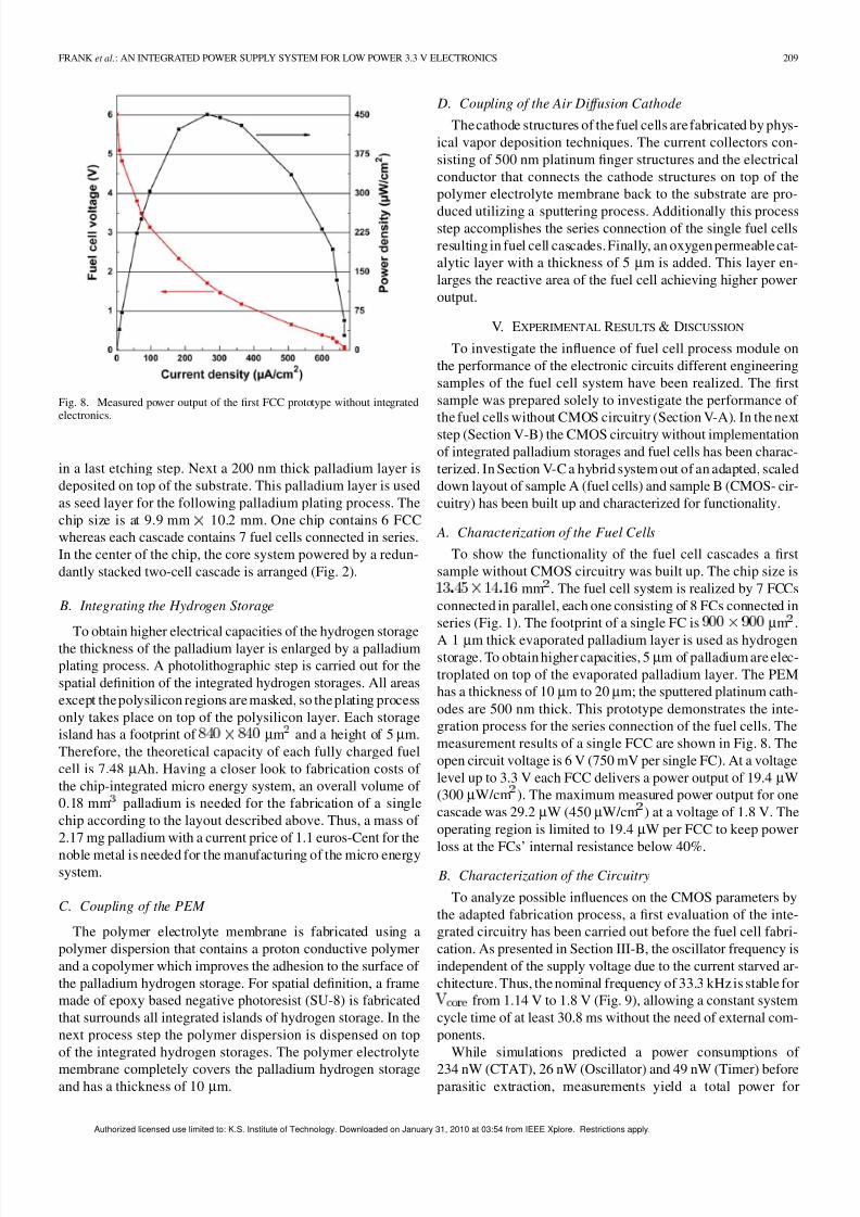
Fig. 8. Measured power output of the first FCC prototype without integratedelectronics.
in a last etching step. Next a 200 nm thick palladium layer is
deposited on top of the substrate. This palladium layer is used
as seed layer for the following palladium plating process. The
chip size is at 9.9 mm 10.2 mm. One chip contains 6 FCC
whereas each cascade contains 7 fuel cells connected in series.
In the center of the chip, the core system powered by a redun-
dantly stacked two-cell cascade is arranged (Fig. 2).
B. Integrating the Hydrogen Storage
To obtain higher electrical capacities of the hydrogen storage
the thickness of the palladium layer is enlarged by a palladium
plating process. A photolithographic step is carried out for the
spatial definition of the integrated hydrogen storages. All areas
except the polysilicon regions are masked, so the plating process
only takes place on top of the polysilicon layer. Each storage
island has a footprint of μm and a height of 5 μm.
Therefore, the theoretical capacity of each fully charged fuel
cell is 7.48 μAh. Having a closer look to fabrication costs of
the chip-integrated micro energy system, an overall volume of
0.18 mm palladium is needed for the fabrication of a single
chip according to the layout described above. Thus, a mass of
2.17 mg palladium with a current price of 1.1 euros-Cent for the
noble metal is needed for the manufacturing of the micro energysystem.
C. Coupling of the PEM
The polymer electrolyte membrane is fabricated using a
polymer dispersion that contains a proton conductive polymer
and a copolymer which improves the adhesion to the surface of
the palladium hydrogen storage. For spatial definition, a frame
made of epoxy based negative photoresist (SU-8) is fabricated
that surrounds all integrated islands of hydrogen storage. In the
next process step the polymer dispersion is dispensed on top
of the integrated hydrogen storages. The polymer electrolyte
membrane completely covers the palladium hydrogen storageand has a thickness of 10 μm.
D. Coupling of the Air Diffusion Cathode
The cathode structures of the fuel cells are fabricated by phys-
ical vapor deposition techniques. The current collectors con-
sisting of 500 nm platinum finger structures and the electrical
conductor that connects the cathode structures on top of the
polymer electrolyte membrane back to the substrate are pro-
duced utilizing a sputtering process. Additionally this processstep accomplishes the series connection of the single fuel cells
resulting in fuel cell cascades. Finally, an oxygen permeable cat-
alytic layer with a thickness of 5 μm is added. This layer en-
larges the reactive area of the fuel cell achieving higher power
output.
V. EXPERIMENTAL RESULTS & DISCUSSION
To investigate the influence of fuel cell process module on
the performance of the electronic circuits different engineering
samples of the fuel cell system have been realized. The first
sample was prepared solely to investigate the performance of
the fuel cells without CMOS circuitry (Section V-A). In the next
step (Section V-B) the CMOS circuitry without implementation
of integrated palladium storages and fuel cells has been charac-
terized. In Section V-C a hybrid system out of an adapted, scaled
down layout of sample A (fuel cells) and sample B (CMOS- cir-
cuitry) has been built up and characterized for functionality.
A. Characterization of the Fuel Cells
To show the functionality of the fuel cell cascades a first
sample without CMOS circuitry was built up. The chip size is
mm . The fuel cell system is realized by 7 FCCs
connected in parallel, each one consisting of 8 FCs connected in
series (Fig. 1). The footprint of a single FC is μm .
A 1 μm thick evaporated palladium layer is used as hydrogenstorage. To obtain higher capacities, 5 μm of palladium are elec-
troplated on top of the evaporated palladium layer. The PEM
has a thickness of 10 μm to 20 μm; the sputtered platinum cath-
odes are 500 nm thick. This prototype demonstrates the inte-
gration process for the series connection of the fuel cells. The
measurement results of a single FCC are shown in Fig. 8. The
open circuit voltage is 6 V (750 mV per single FC). At a voltage
level up to 3.3 V each FCC delivers a power output of 19.4 μW
(300 μW/cm ). The maximum measured power output for one
cascade was 29.2 μW (450 μW/cm ) at a voltage of 1.8 V. The
operating region is limited to 19.4 μW per FCC to keep power
loss at the FCs’ internal resistance below 40%. B. Characterization of the Circuitry
To analyze possible influences on the CMOS parameters by
the adapted fabrication process, a first evaluation of the inte-
grated circuitry has been carried out before the fuel cell fabri-
cation. As presented in Section III-B, the oscillator frequency is
independent of the supply voltage due to the current starved ar-
chitecture. Thus, the nominal frequency of 33.3 kHz is stable for
from 1.14 V to 1.8 V (Fig. 9), allowing a constant system
cycle time of at least 30.8 ms without the need of external com-
ponents.
While simulations predicted a power consumptions of
234 nW (CTAT), 26 nW (Oscillator) and 49 nW (Timer) beforeparasitic extraction, measurements yield a total power for
Authorized licensed use limited to: K.S. Institute of Technology. Downloaded on January 31, 2010 at 03:54 from IEEE Xplore. Restrictions apply.

8/7/2019 An Integrated Power Supply System for Low Power
http://slidepdf.com/reader/full/an-integrated-power-supply-system-for-low-power 6/9
210 IEEE JOURNAL OF SOLID-STATE CIRCUITS, VOL. 45, NO. 1, JANUARY 2010
Fig. 9. Measured oscillator frequency and power consumption for varyingsupply voltage.
Fig. 10. Measured duration and energy consumption for one fuel cell check.
this core system of 620 nW ( V, C for
simulation and measurement). This significant difference can
be explained by the large parasitic leakage current due to the
CTAT’s n-well resistors of approximately 70 M .
For characterization of the bypass system presented in
Section III-C the duration and energy consumption of a single
fuel cell check is chosen. Both values depend on the cell’s
position within the cascade and thereby on (Fig. 10). It
follows, that one FCC check takes approximately 626 μs with
an average energy consumption of 220 pWs for each FCC,
assuming an open circuit voltage of 700 mV for each of theseven fuel cells per cascade. All cascades are checked in
parallel. In case of defective and hence shorted fuel cells the
resistance of the transmission gates varies from 200 to
1.2 k . The increase is observed for cells in the middle of the
stack caused by the transmission gates body effect. Assuming
a maximum power output of 31.4 μW per cascade, causes
a worst-case voltage drop of 11.4 mV. The maximum power
output was chosen to match the measurement results presented
in Section V-C.
Measurements yield a power consumption of 9.6 μW for the
LDO, whereas simulations predicted 8.3 μW. The LDO’s refer-
ence voltage is derived from the oscillator’s CTAT, consuming
additional 24 nW in simulations. Hence, this contribution canbe neglected.
Fig. 11. Measured line regulation for the implemented LDO with swept butideal input voltage.
Fig. 12. Measured load regulation for the implemented LDO with constantinput voltage ( V = 3 : 5 V) .
Measurements of the line and load regulation can be seen in
Fig. 11 & Fig. 12, respectively, where the FCCs are replaced by
a swept input voltage or a constant voltage of 3.5 V, respectively.
With all FCCs in parallel (replaced by ideal voltage sources of
3.5 V) a current efficiency of 92% can be achieved if loaded
with 32.2 μA (Fig. 13), which is the maximum measured output
current of the hybrid system with an output voltage drop of less
than 10% as presented later in Section V-C. The said current
efficiency is calculated as the output current normalized to the
input current of the LDO. Therefore, the fuel cell losses and
the pass elements’ voltage drop are not taken into account. The
efficiency is a measure of the control system’s (oscillator, timer
& LDO) quiescent current with respect to the available output
power.
C. Characterization of the Hybrid System
A hybrid system has been set up to verify the functionality
of the integrated circuitry powered by the fuel cells (Fig. 14).
Using the scaled down layout of the fully integrated system
with 6 cascades consisting of 7 fuel cells each and CMOS-elec-
tronics, two chips have been fabricated. The first chip featuresthe completely functional electronic devices without fuel cells,
Authorized licensed use limited to: K.S. Institute of Technology. Downloaded on January 31, 2010 at 03:54 from IEEE Xplore. Restrictions apply.

8/7/2019 An Integrated Power Supply System for Low Power
http://slidepdf.com/reader/full/an-integrated-power-supply-system-for-low-power 7/9

8/7/2019 An Integrated Power Supply System for Low Power
http://slidepdf.com/reader/full/an-integrated-power-supply-system-for-low-power 8/9
212 IEEE JOURNAL OF SOLID-STATE CIRCUITS, VOL. 45, NO. 1, JANUARY 2010
Therefore, the reaction kinetics is much slower but the perfor-
mance of the chip-integrated fuel cell is competitive to state-of
the-art wafer level power supplies.
VI. CONCLUSION
The hybrid integration of a chip-integrated micro energy
system based on fuel cells and a CMOS control circuitry that
stabilizes the output voltage of the system to a constant level
of 3.3 V was demonstrated successfully. At a voltage level of
3.3 V the system has a power density of 440 μW/cm referring
to the active chip area covered by fuel cells. In sleep mode, a
core system with a power consumption of 620 nW enables a
periodic system wake-up after a preset time adjustable between
30 ms and 4 years. In active mode the output voltage is stabi-
lized to 3.3 V up to a power consumption of 54.5 μW, which
relates to a current efficiency of 92%.
In future work the monolithic integration of fuel cell cascades
and the electronic control circuitry will be realized. A detailed
characterization of the fully integrated system with fuel cell cas-
cades and the CMOS circuitry on a single chip will be carriedout. Further integration of a sensor and a signal processing unit
will allow the realization of autonomous sensor devices.
ACKNOWLEDGMENT
This research and development project is funded by the
German Federal Ministry of Education and Research (BMBF)
within the funding number 02PG2420 and managed by the
Project Management Agency Karlsruhe (PTKA).The author is
responsible for the contents of this publication.
REFERENCES
[1] B. Warnecke and K. Pister, “An ultra-low energy microcontroller for
smart dust wireless sensor networks,” in IEEE ISSCC Dig. Tech. Pa- pers, Feb. 15–19, 2004.
[2] G. Erdler et al., “Chip integrated fuel cell,” Sensors and Actuators A,vol. 132, pp. 331–336, Nov. 2006.
[3] R. W. Cahn, “Electronic and magnetic properties of metals and ce-ramics part II,” Materials Sci. Technol., vol. 3B, p. 298, 1994.
[4] N. Dudney, “Solid-state thin-film rechargeable batteries,” Materials
Sci. Eng. B, vol. 116, pp. 245–249, 2005.[5] L. Lehmann, W. Baumann, R. Ehret, M. Brischwein, H. J. Gahle, and
G. Igel, “CMOS-based cellular biosensor in process and application,” Micro-Syst. Technol., pp. 207–212, 1998.
[6] G. Igel and H. J. Gahle, “Process for manufacturing a sensor with ametal electrode in a metal oxide semiconductor (MOS) structure,” U.S.patent 6,017,775, Jan. 25, 2000.
[7] R. Hahn etal., “Development of near hermetic silicon/glass cavities forpackaging of integrated lithium micro batteries,” in Proc. DTIP MEMS
& MOEMS, 2009.[8] J. Song et al., “Solid-state microscale lithium batteries prepared withmicrofabrication processes,” J. Micromech. Microeng., vol. 19, 2009.
[9] H. Banba et al., “A CMOS bandgap reference circuit with sub-1-Voperation,” IEEE J. Solide-State Circuits, vol. 34, no. 5, pp. 670–674,May 1999.
Mirko Frank received a certificate of appren-ticeship as a toolmaker at the company WalterSöhner GmbH & Co. KG, Germany, in 1998, andthe Dipl.-Ing. degree in microsystems engineeringfrom the University of Freiburg in 2005. He iscurrently working toward the Ph.D. degree in theDepartment of Microsystems Engineering at theUniversity of Freiburg. His main research interestsare chip integrated fuel cells and rechargeable fuelcell accumulators.
Matthias Kuhl received the B.Sc. and M.Sc. de-grees in electrical engineering from the University of Wuppertal, Germany, in 2004and 2006, respectively.Since 2006, he is a Ph.D. student at the University of Freiburg, Germany, working in the microelectronicsgroup from Prof. Manoli. His research topics includethe design of autonomous microsystems as well aslow power architectures.
Gilbert Erdler received the Dipl.-Ing. degree inmicrosystems engineering from the University of Freiburg, Germany, in 2004. From 2004 until 2007he was a graduate researcher in the Departmentof Microsystems Engineering at the University of Freiburg, Germany and received his Ph.D. degree inmicrosystems engineering in 2007.
Since 2007 he has been with the Micronas GmbHin Freiburg, Germany. His mainresearch interests aremicro fuel cells and MEMS engineering.
Ingo Freund graduated in electrical engineeringfrom the University of Applied Sciences of Furt-wangen, German,y in 1998.
From 1998 to 2000 he was graduate researcher atUniversities of Freiburg and Rostock in Germany.In 2000 he joined Micronas GmbH as a conceptengineer. Since 2007 he has been responsible for predevelopment within Micronas. His main interestsconcern “More Than Moore” strategies for semicon-ductor companies.
Yiannos Manoli received the B.A. degree (summa
cum laude) in physics and mathematics from
Lawrence University, Appleton, Wisconsin, in 1978,and the M.S. degree in electrical engineering andcomputer science from the University of Californiaat Berkeley in 1980. He received the Dr.-Ing. Degreein electrical engineering from the Gerhard MercatorUniversity, Duisburg, Germany, in 1987.
From 1980 to 1984, he was a Research Assistantat the University of Dortmund, Germany, in the fieldof digital and analog CMOS integrated circuit design
with an emphasis on analog-to-digital and digital-to-analog converters. In 1985,he joined the newly founded Fraunhofer Institute of Microelectronic Circuitsand Systems, Duisburg, Germany, where he established a design group workingon mixed-signalCMOS circuits especially for monolithic integrated sensors andapplication specific microcontrollers. From 1996 to 2001, he held the Chairof Microelectronics as full professor with the Department of Electrical Engi-neering, University of Saarland, Saarbrücken, Germany. In July 2001, he wasappointed Chair of Microelectronics, Department of Microsystems Engineering
(IMTEK), University of Freiburg, Germany. Since May 2005, he has served asoneof thethree directorsat theInstitute of Microand InformationTechnology of the Hahn-Schickard Gesellschaft (HSG-IMIT), Villingen-Schwenningen, Ger-many. His current research interests are the design of low-voltage/low-powermixed-signal CMOS circuits, electronics for energy harvesting and embeddedmicrosystems, sensor read-out circuits as well as A/D-converters. In 2000, hehad the opportunity to spend half a year on a research project with Motorola(now Freescale) in Phoenix, AZ. In 2006, he spent his sabbatical semester withIntel, Santa Clara, CA, working on the read-out electronics for a high-resolutionaccelerometer.
Prof. Manoli received the Best Paper Award from the European Solid-StateCircuits Conference (ESSCIRC 1988) for the paper “A Self-Calibration Methodfor Fast High-Resolution A/D and D/A Converters.” His group has receivedawards at the Workshop on Micro and Nanotechnology for Energy Applica-tions (PowerMEMS 2006), at the IEEE International Midwest Symposium onCircuits and Systems (MWSCAS 2007), and at the IEEE International Confer-
ence on Microelectronic Systems Education (MSE-2007). The last award was
Authorized licensed use limited to: K.S. Institute of Technology. Downloaded on January 31, 2010 at 03:54 from IEEE Xplore. Restrictions apply.

8/7/2019 An Integrated Power Supply System for Low Power
http://slidepdf.com/reader/full/an-integrated-power-supply-system-for-low-power 9/9
FRANK et al.: AN INTEGRATED POWER SUPPLY SYSTEM FOR LOW POWER 3.3 V ELECTRONICS 213
dedicated to the project Spicy VOLTsim (www.imtek.de/svs) a web-based ap-plication for the animation and visualization of analog circuits which also re-ceived the Multi-Media-Award of the University of Freiburg in 2005. When thefaculty introduced the Best Teaching Award in 2008 Professor Manoli was thefirst toreceivethishonor. Prof. Manolihas servedon thecommitteesof a numberof conferences such as ISSCC, ESSCIRC, DATE and ICCD, and was ProgramChair (2001) and General Chair (2002) of the IEEE International Conference onComputer Design (ICCD). He is a member of Mortar Board, Phi Beta Kappa,
IEEE, VDE and of the Editorial Board of the Journal of Low Power Electronics.
Claas Müller studied physics from 1986 to 1991 atthe University of Karlsruhe. Following the physicsdiploma, he earned his doctorate in 1994 at theForschungszentrum Karlsruhe, Institute for MicroStructure Technology, for his work on a minia-turized spectrometer system, fabricated by LIGAtechnology. Meanwhile, the micro spectrometer isintroduced to a broad range of industrial applicationsby the company microParts. At the Forschungszen-trum, the prerequisites for a small scale productionwere achieved. As a responsible project manager,
Dr. Müller was considerably involved in these activities.Since 1996, he has been an academic director at the Chair of Process Tech-
nology of the IMTEK. In 1999, he was appointed substitutional manager, andin 2004, the managing director of the Chair of Process Technology.
Holger Reinecke was born in 1964 in Bad Harzburg,Germany. From 1983 to 1988, he studied Chemistryat the Technical University at Clausthal-Zellerfeld.From 1988 to 1990, he was scientific assistant at theInstitute for Inorganic and Analytical Chemistry, andgraduated in the field of electrochemical analytics in1990.
In August1990,hestarted as a scientificassistant at
the company microParts GmbH in the electroplatinggroup, which he became head of in 1991. From 1993,he tookover the department of chemical process tech-
nology, and the complete department of process technology in 1995. Duringthis time, he developed, qualified and established processes for the fabricationof micro structured components and tools. Among other things, lithographical,electro-chemical, vacuum- or laser technical methods were implemented. Fur-thermore, he has established complete process chains for mass production of silicon based medical products as well as for cleaning and surface coating of polymeric components. These components were used in medical devices. Theseprocesses were designed, installed, validated and operated according to medicaland pharmaceutical requirements of European and American approval author-ities. In 1999, as an area manager he additionally became head of the productbranches micro fluidics and micro optics. Since November 2004, he is Headof the Chair of Process Technology at the Department of Micro Systems Engi-neering (IMTEK) at University of Freiburg.Additionally, since May 2005 he hasbeen Speaker of the Board of Directors of the HSG-IMIT in Villingen-Schwen-
ningen (www.hsg-imit.de).