An FPGA-Based Hardware Accelerator For The Digital Image ...
140
University of Arkansas, Fayetteville University of Arkansas, Fayetteville ScholarWorks@UARK ScholarWorks@UARK Graduate Theses and Dissertations 5-2020 An FPGA-Based Hardware Accelerator For The Digital Image An FPGA-Based Hardware Accelerator For The Digital Image Correlation Engine Correlation Engine Keaten Stokke University of Arkansas, Fayetteville Follow this and additional works at: https://scholarworks.uark.edu/etd Part of the Hardware Systems Commons, Numerical Analysis and Scientific Computing Commons, and the Signal Processing Commons Citation Citation Stokke, K. (2020). An FPGA-Based Hardware Accelerator For The Digital Image Correlation Engine. Graduate Theses and Dissertations Retrieved from https://scholarworks.uark.edu/etd/3664 This Thesis is brought to you for free and open access by ScholarWorks@UARK. It has been accepted for inclusion in Graduate Theses and Dissertations by an authorized administrator of ScholarWorks@UARK. For more information, please contact [email protected].
Transcript of An FPGA-Based Hardware Accelerator For The Digital Image ...

University of Arkansas, Fayetteville University of Arkansas, Fayetteville
ScholarWorks@UARK ScholarWorks@UARK
Graduate Theses and Dissertations
5-2020
An FPGA-Based Hardware Accelerator For The Digital Image An FPGA-Based Hardware Accelerator For The Digital Image
Correlation Engine Correlation Engine
Keaten Stokke University of Arkansas, Fayetteville
Follow this and additional works at: https://scholarworks.uark.edu/etd
Part of the Hardware Systems Commons, Numerical Analysis and Scientific Computing Commons,
and the Signal Processing Commons
Citation Citation Stokke, K. (2020). An FPGA-Based Hardware Accelerator For The Digital Image Correlation Engine. Graduate Theses and Dissertations Retrieved from https://scholarworks.uark.edu/etd/3664
This Thesis is brought to you for free and open access by ScholarWorks@UARK. It has been accepted for inclusion in Graduate Theses and Dissertations by an authorized administrator of ScholarWorks@UARK. For more information, please contact [email protected].

An FPGA-Based Hardware Accelerator For The Digital Image Correlation Engine
A thesis submitted in partial fulfillmentof the requirements for the degree of
Master of Science in Computer Engineering
by
Keaten StokkeUniversity of Arkansas
Bachelors of Science in Computer Engineering, 2018
May 2020University of Arkansas
This thesis is approved for recommendation to the Graduate Council.
David Andrews, PhDThesis Director
Patrick Parkerson, PhD Dale Thompson, PhDCommittee Member Committee Member

Abstract
The work presented in this thesis was aimed at the development of a hardware accelerator
for the Digital Image Correlation engine (DICe) and compare two methods of data access,
USB and Ethernet. The original DICe software package was created by Sandia National
Laboratories and is written in C++. The software runs on any typical workstation PC and
performs image correlation on available frame data produced by a camera. When DICe is
introduced to a high volume of frames, the correlation time is on the order of days. The
time to process and analyze data with DICe becomes a concern when a high-speed camera,
like the Phantom VEO 1310, is used which is capable of recording up to 10,000 Frames Per
Second (FPS) [1]. To reduce this correlation time the DICe software package was ported over
to Verilog, and a Xilinx UltraScale+ MPSoC ZCU104 FPGA was targeted for the design.
FPGAs are used to implement the hardware accelerator due to their hardware-level speeds
and reprogrammability. The ZCU104 board contains FPGA fabric on the Programmable
Logic (PL) side that is used for the implementation of the ported DICe hardware design. On
the Processing System (PS) side of the ZCU104, a quad-core ARM Cortex-A53 processor
is available that runs the Ubuntu 18.04 LTS Linux-based kernel to provide the drivers for
USB and Ethernet I/O, a standard file system that is accessed through a Command-Line
Interface (CLI), and to run the program’s control scripts that are written in C. This work
compares the processing time of the DICe hardware accelerator when frame data is accessed
via Ethernet-stream or local USB to showcase the fastest option when using DICe. Both
methods of accessing frame data are necessary because data may be offloaded from the
camera over Ethernet while it is still recording, or the frame data may be readily available
in memory. By providing both a method to access frame data via USB and Ethernet, users
have more flexibility when using the DICe hardware accelerator. The work presented in this
thesis is significant because it is the first known hardware accelerator for the DICe software.

©2020 by Keaten StokkeAll Rights Reserved

Acknowledgements
I would like to thank the University of Arkansas and the faculty of the Computer Science
and Computer Engineering Department for providing me and many other students with the
tools and skills that we need to succeed. I could not have asked for a better university,
department, or faculty to provide me with my education. The Department of Computer
Science and Computer Engineering has been my home for the last six years and I will
miss my time here. I also want to extend my gratitude to Dr. David Andrews, Dr. Dale
Thompson, and Dr. Patrick Parkerson for supporting me as members of my committee. I
have a great deal of respect for each of these professors and I am grateful for all they have
taught me during my undergraduate and graduate careers.
I want to give special thanks to my thesis advisor, Dr. David Andrews, for guiding me
through this degree. His extensive knowledge and expertise in the field of reconfigurable
computing have taught me a significant amount. Without his support, I would not have
had the opportunity or desire to pursue this degree. From teaching me in the classroom to
pushing me in the research lab, he has been a consistent source of knowledge and wisdom.
Dr. Andrews has presented me with countless opportunities that have positively shaped my
life and I will be forever grateful to him.
I owe a debt of gratitude to Honeywell FM&T for presenting our research lab with the
opportunity to work on the project that led to this thesis. Honeywell FM&T provided my
colleague Atiyeh and me with the funding and work that allowed us to pursue our graduate
degrees. Working with the faculty at Honeywell FM&T, specifically with Mr. Dennis Stanley,
provided us with a wealth of knowledge that has made us better engineers.
I also want to thank my colleague, Atiyehsadat Panahi, for supporting me and working
with me throughout my two years of graduate school. I could not have made it this far
without her assistance. Together we have accomplished many goals and solved countless
problems and my education will forever benefit from our time as partners. Atiyeh is one of
the hardest working and most persistent students I have ever worked with and I thank her

for instilling this work ethic in me.
Finally, I would like to thank my family and friends who have all supported me every
step of the way to achieving this goal. Starting and finishing this degree would not have
been possible without every one of them. With far too many names to list, I want to take
this opportunity to express to my friends how grateful I am for their support and motivation
during the most intense part of my life thus far. As I close this chapter in my life I know
that they will continue to support me in my future endeavors.

Dedication
To my mother, who pushed me to pursue the dreams I thought were impossible
To my father, who raised me to work my hardest under difficult circumstances
To my brother, who showed me that anything is possible with determination
To my sister, who motivated me to push through any obstacle
This thesis and my many years of education are the results of the support that you each
have given me. Thank you for being there for me when I needed it most.
I love you all.

Contents
1 Introduction 1
1.1 Motivation . . . . . . . . . . . . . . . . . . . . . . . . . . . . . . . . . . . . 2
1.2 Thesis Contributions . . . . . . . . . . . . . . . . . . . . . . . . . . . . . . . 4
1.3 Thesis Structure . . . . . . . . . . . . . . . . . . . . . . . . . . . . . . . . . 6
2 Background 8
2.1 DICe . . . . . . . . . . . . . . . . . . . . . . . . . . . . . . . . . . . . . . . 8
2.2 Related Works . . . . . . . . . . . . . . . . . . . . . . . . . . . . . . . . . . 10
3 Platforms 14
3.1 Hardware . . . . . . . . . . . . . . . . . . . . . . . . . . . . . . . . . . . . . 15
3.1.1 Xilinx Zynq UltraScale+ MPSoC FPGA . . . . . . . . . . . . . . . . 19
3.2 Software . . . . . . . . . . . . . . . . . . . . . . . . . . . . . . . . . . . . . . 25
3.2.1 Vivado 2018.3 . . . . . . . . . . . . . . . . . . . . . . . . . . . . . . 26
3.2.2 Vivado 2018.3 SDK . . . . . . . . . . . . . . . . . . . . . . . . . . . 30
3.2.3 PetaLinux . . . . . . . . . . . . . . . . . . . . . . . . . . . . . . . . 32
4 Application Design 38
4.1 DICe Hardware Design . . . . . . . . . . . . . . . . . . . . . . . . . . . . . 38
4.1.1 Miscellaneous IPs . . . . . . . . . . . . . . . . . . . . . . . . . . . . 43
4.1.2 BRAM IPs . . . . . . . . . . . . . . . . . . . . . . . . . . . . . . . . 46
4.1.3 Parameters IP . . . . . . . . . . . . . . . . . . . . . . . . . . . . . . 47
4.1.4 Interface IP . . . . . . . . . . . . . . . . . . . . . . . . . . . . . . . . 51
4.1.5 Subset Coordinates Interface IP . . . . . . . . . . . . . . . . . . . . 53
4.1.6 Subset Coordinates IP . . . . . . . . . . . . . . . . . . . . . . . . . . 55
4.1.7 Gradients IP . . . . . . . . . . . . . . . . . . . . . . . . . . . . . . . 61
4.1.8 Gamma Interface IP . . . . . . . . . . . . . . . . . . . . . . . . . . . 67

4.1.9 Gamma IP . . . . . . . . . . . . . . . . . . . . . . . . . . . . . . . . 69
4.1.10 Results IP . . . . . . . . . . . . . . . . . . . . . . . . . . . . . . . . 73
4.2 DICe Software Design . . . . . . . . . . . . . . . . . . . . . . . . . . . . . . 74
4.2.1 C Client Script . . . . . . . . . . . . . . . . . . . . . . . . . . . . . . 75
4.2.2 C Server Script . . . . . . . . . . . . . . . . . . . . . . . . . . . . . . 79
5 Results 84
5.1 Python-Based Control Script Performance . . . . . . . . . . . . . . . . . . . 84
5.2 C-Based Control Script Performance . . . . . . . . . . . . . . . . . . . . . . 89
5.3 USB-based Design . . . . . . . . . . . . . . . . . . . . . . . . . . . . . . . . 95
5.4 Ethernet-Based Design . . . . . . . . . . . . . . . . . . . . . . . . . . . . . . 97
5.5 DICe Hardware Design Performance . . . . . . . . . . . . . . . . . . . . . . 100
5.6 Floating-Point Library Performance . . . . . . . . . . . . . . . . . . . . . . 104
6 Discussion 108
6.1 PetaLinux vs. lwIP . . . . . . . . . . . . . . . . . . . . . . . . . . . . . . . 108
6.2 Challenges . . . . . . . . . . . . . . . . . . . . . . . . . . . . . . . . . . . . 115
6.3 Future Work . . . . . . . . . . . . . . . . . . . . . . . . . . . . . . . . . . . 118
7 Conclusion 121
7.1 Bibliography . . . . . . . . . . . . . . . . . . . . . . . . . . . . . . . . . . . . 122

List of Figures
3.1 The physical layout for the ZCU104 FPGA [2] . . . . . . . . . . . . . . . . 20
3.2 A diagram of the PS and PL sections of the ZCU104 device [3] . . . . . . . 21
3.3 The physical layout for the KC705 FPGA [4] . . . . . . . . . . . . . . . . . 22
3.4 The physical layout for the VC707 FPGA [5] . . . . . . . . . . . . . . . . . 23
4.1 A simple flow diagram of the DICe hardware design . . . . . . . . . . . . . 39
4.2 A graphical representation of the differences found between the reference frame
(left) and the deformed frame (right) in DICe [6] . . . . . . . . . . . . . . . 42
4.3 The block diagram for the top half of the DICe hardware accelerator in Vivado
2018.3 . . . . . . . . . . . . . . . . . . . . . . . . . . . . . . . . . . . . . . . 43
4.4 The block diagram for the bottom half of the DICe hardware accelerator in
Vivado 2018.3 . . . . . . . . . . . . . . . . . . . . . . . . . . . . . . . . . . 43
4.5 A table from Vivado 2018.3 showing the defined memory addresses and sizes
for each IP used in the DICe hardware design . . . . . . . . . . . . . . . . . 48
4.6 A graphical representation of a subset (in red) is defined within a 448x232
frame . . . . . . . . . . . . . . . . . . . . . . . . . . . . . . . . . . . . . . . 56
4.7 A graphical representation of multiple subsets defined within a 448x232 frame 57
4.8 A graphical representation of square subset as described in example 1 . . . . 58
4.9 A graphical representation of circular subset as described in example 2 . . . 60
4.10 Definition of terms used in the local DIC formulation [7] . . . . . . . . . . . 63
5.1 A snapshot from the PCs CLI of the Python script opening a single 448x232
frame and retrieving all of its pixel values . . . . . . . . . . . . . . . . . . . 85
5.2 A snapshot from the PCs CLI of the Python script opening a single 448x232
frame, retrieving all of its pixel values, and transferring them to the ZCU104
FPGA via Gigabit Ethernet . . . . . . . . . . . . . . . . . . . . . . . . . . . 86

5.3 A snapshot from the PCs CLI of the Python script opening a single 448x232
frame, retrieving all of its pixel values, and converting them to IEEE-754
single-precision floating-point format . . . . . . . . . . . . . . . . . . . . . . 87
5.4 A snapshot from the PCs CLI of the Python script opening a single 448x232
frame, retrieving all of its pixel values, converting them to IEEE-754 single-
precision floating-point format, and transferring them to the FPGA over Gi-
gabit Ethernet . . . . . . . . . . . . . . . . . . . . . . . . . . . . . . . . . . 89
5.5 A snapshot from the PCs CLI of the C script opening a single 448x232 frame
and retrieving all of its pixel values . . . . . . . . . . . . . . . . . . . . . . . 90
5.6 A snapshot from the PCs CLI of the C script opening a single 448x232 frame,
retrieving all of its pixel values, and transferring them to the ZCU104 FPGA
via Gigabit Ethernet . . . . . . . . . . . . . . . . . . . . . . . . . . . . . . . 91
5.7 A snapshot from the PCs CLI of the C script opening a single 448x232 frame,
retrieving all of its pixel values, and converting them to IEEE-754 single-
precision floating-point format . . . . . . . . . . . . . . . . . . . . . . . . . 92
5.8 A snapshot from the PCs CLI of the C script opening a single 448x232 frame,
retrieving all of its pixel values, converting them to IEEE-754 single-precision
floating-point format, and transferring them to the ZCU104 FPGA via Gigabit
Ethernet . . . . . . . . . . . . . . . . . . . . . . . . . . . . . . . . . . . . . 93
5.9 A snapshot from the FPGAs CLI of the C script opening a single 448x232
frame and retrieving all of its pixel values . . . . . . . . . . . . . . . . . . . 93
5.10 A snapshot from the FPGAs CLI of the C script opening a single 448x232
frame, retrieving all of its pixel values, and converting them to IEEE-754
single-precision floating-point format . . . . . . . . . . . . . . . . . . . . . . 94
5.11 A snapshot from the FPGAs CLI of the read speeds from the USB drive on
the ZCU104 FPGA . . . . . . . . . . . . . . . . . . . . . . . . . . . . . . . 96

5.12 A snapshot from the FPGAs CLI of the write speeds from the USB drive on
the ZCU104 FPGA . . . . . . . . . . . . . . . . . . . . . . . . . . . . . . . 97
5.13 A snapshot from the PCs CLI of the Ethernet network speed from the PC to
the ZCU104 FPGA . . . . . . . . . . . . . . . . . . . . . . . . . . . . . . . 98
5.14 A snapshot from the FPGAs CLI of the Ethernet network speed from the
ZCU104 FPGA to the PC . . . . . . . . . . . . . . . . . . . . . . . . . . . . 99
5.15 A graph of the resource utilization for the DICe hardware design on the
ZCU104 FPGA . . . . . . . . . . . . . . . . . . . . . . . . . . . . . . . . . . 101
5.16 A line graph that shows the total execution time of the DICe hardware accel-
erator in reference to the number of frames, the number of subsets, and the
size of the subsets . . . . . . . . . . . . . . . . . . . . . . . . . . . . . . . . 103
5.17 A bar graph that shows the total execution time per frame of the DICe hard-
ware accelerator in reference to the number of frames, the number of subsets,
and the size of the subsets . . . . . . . . . . . . . . . . . . . . . . . . . . . . 104
5.18 A block diagram of the addition function in the floating-point library . . . . 106
5.19 Comparison of the proposed and the previous basic floating-point arithmetic
functions (a) Delay (b) LUTs (c) FFs . . . . . . . . . . . . . . . . . . . . . 107
6.1 A graphical representation of an obstruction within the frames in DICe [6] . 119

List of Tables
3.1 Programmable logic features for the ZCU104 FPGA [8] . . . . . . . . . . . . 21
3.2 Programmable logic features for the Kintex-7 and Virtex-7 FPGAs [9, 10] . . 24
5.1 Performance comparisons between the Python-based and C-based control scripts 94
5.2 Ethernet performance comparisons between FPGAs . . . . . . . . . . . . . . 100
5.3 The available and utilized resources for the DICe hardware design on the
ZCU104 FPGA . . . . . . . . . . . . . . . . . . . . . . . . . . . . . . . . . . 100
5.4 Performance comparisons between DICe execution methods . . . . . . . . . . 102

Listings
3.1 Terminal command to create a new PetaLinux project [11] . . . . . . . . . . 34
3.2 Terminal command to configure the PetaLinux project with the hardware
design [11] . . . . . . . . . . . . . . . . . . . . . . . . . . . . . . . . . . . . . 35
3.3 Terminal command to package the PetaLinux project [11] . . . . . . . . . . . 35
3.4 Configuration of the FPGAs Ethernet and USB device drivers in the system-
user.dtsi file [12] . . . . . . . . . . . . . . . . . . . . . . . . . . . . . . . . . . 36
4.1 C++ code to compute circular subset coordinate pixels from the DICe source
code [6] . . . . . . . . . . . . . . . . . . . . . . . . . . . . . . . . . . . . . . 62
4.2 C++ code to compute the gradients from the pixel intensities from the DICe
source code [6] . . . . . . . . . . . . . . . . . . . . . . . . . . . . . . . . . . . 66
4.3 Reading from USB memory in C . . . . . . . . . . . . . . . . . . . . . . . . 80
4.4 Converting a decimal value to the IEEE-754 single-precision floating-point
format in C . . . . . . . . . . . . . . . . . . . . . . . . . . . . . . . . . . . . 81
4.5 Converting individual pixels to the IEEE-754 format and writing them to
BRAM in C . . . . . . . . . . . . . . . . . . . . . . . . . . . . . . . . . . . . 82
5.1 Python code for retrieving pixel intensity values from the image and converting
it to the IEEE-754 single-precision floating-point format . . . . . . . . . . . 88

Chapter 1
Introduction
Digital Image Correlation (DIC) is an optical method implemented by computers that
receive image frames as input and measures the deformation on an object’s surface without
contact [13]. DIC works by comparing digital photographs of a component or test piece at
different stages of deformation. By tracking blocks of pixels, the system can measure surface
displacement and build up a full field 2D and 3D deformation vector fields and strain maps
[13–16]. Rather than individual pixels providing a reference point for measuring the change
of an object from frame to frame, the neighboring pixels of that point is used to provide a
reference window or subset, that can provide far more accurate measurements for analysis
[7, 17]. DIC is becoming more common in everyday applications such as automotive use for
self-driving cars to process their environment and avoid obstacles or industrial applications
that analyze small components for abnormal wear, tear, and defections [14]. The increase
in modern applications that depend on DIC to properly function means an increase of the
computational devices needed to perform DIC in a suitable time frame, especially with the
development of Real-Time Systems (RTS) where accurate results in a short amount of time
are a necessity.
Field-Programmable Gate Arrays (FPGAs) have long been used for their flexibility to
create reprogrammable designs that target physical hardware for accelerating application
performance [18]. For high-level applications that have frequently changing parameters, the
use of Application-Specific Integrated Circuits (ASICs) become a burden by their inability
to implement functional changes in their hardware designs. FPGAs provide an option for
developers to create applications that can be modified and reprogrammed in the boards
Configurable Logic Blocks (CLBs) to achieve near-true hardware acceleration without the
expense of manufacturing and redeploying physical ASIC chips. FPGAs have been used for
decades, but recently they have made a big come back due to the large volume of high-
1

level applications that require both accelerated performance and configurable designs [18].
Many modern FPGA’s contain components such as multi-core hard-processors, Graphics
Processing Units (GPUs), and various I/O ports that can interact with the low-level hardware
designs in the FPGAs’ fabric [8]. This makes modern System-on-Chip (SoC) FPGAs more
capable for processing-intensive applications than ever before.
The work presented in this thesis combines the use of FPGAs for accelerated hardware
performance and the Digital Image Correlation engine (DICe) program as the high-level
application to leverage the performance boost. DICe is an open-source tool that intends
to provide users with either a DIC module to implement in external applications or as a
standalone analysis program [6]. Currently, the DICe Graphical User Interface (GUI) only
supports basic use cases for 2D and stereo DIC. Additional features can be enabled through
the Command-Line Interface (CLI) to support use for additional DIC methods, such as
trajectory tracking. When DICe is presented with a large volume of frames to process with
multiple subsets, the time to complete DIC on the data set can be on the order of days for
a standard workstation computer. This lengthy delay in producing results is unacceptable
to many users of DICe, whom all desire a means to produce results faster. A delay in
producing and analyzing the results of DIC from DICe leads to a delay to solve the larger
engineering problems that the application was meant to solve. The work in this thesis is
aimed at the development of a hardware accelerator for the DICe software by porting the
design to the Verilog Hardware Description Language (HDL) to target FPGAs’ for the core
of the processing of the application.
1.1 Motivation
The Honeywell FM&T facility has a close relationship with Sandia National Laboratories
out in Albuquerque, NM, the lab responsible for the creation of DICe. The driving force
behind the work presented in this thesis came from the engineers at Honeywell FM&T who
needed the DICe application to perform image correlation at a faster rate. The Honeywell
2

FM&T facility is tasked with manufacturing a wide range of components and products for the
Department of Energy (DOE) that are critical to the defense of the United States. DICe is
used by these engineers to analyze the tools Honeywell uses to manufacture these products,
as well as the products themselves. The failure of a simple component produced by this
facility can result in the loss of American lives, which is unacceptable.
The engineers at Honeywell FM&T have been exploring more ways to apply FPGAs to
computational problems within the facility through in-house and out-of-house Research &
Development (R&D) projects. This resulted in Honeywell tasking the Computer Systems
Design Laboratory at the University of Arkansas with exploring the development of a hard-
ware accelerator for DICe. One of the primary focuses of the Computer Systems Design
Laboratory is to use FPGAs as hardware accelerators for various applications. FPGAs are
very well suited for correlation computation and have been shown to improve performance
by orders of magnitude with respect to software implementations on PCs [19, 20].
The work presented in this thesis is a direct result of the statement of work that was
provided by Honeywell FM&T. This thesis presents an FPGA-based hardware accelerator
for the DICe application. By porting the C++-based DICe source code to Verilog, a Zynq
UltraScale+ MPSoC FPGA was targeted to execute the application. The work in this thesis
is the first known example of a DICe hardware accelerator. The resulting application can
perform image correlation by accessing frame data either from a USB drive or an Ethernet-
based connection. These two options for data access provides the users with the flexibility
to run the application on available data that already exists within the memory of a USB
drive, or stream the data to the application from the camera to the FPGA, where the FPGA
acts as a “bump-in-the-wire” solution. While developing the DICe hardware accelerator, a
novel low-latency library for arithmetic and trigonometric functions was created for FPGAs’
to accelerate the simple mathematical operations within the image correlation algorithms
[21]. This work provides an alternative solution when compared to existing libraries, that
is optimized for sequential operations, designs where low-latency is a priority over high-
3

throughput, and designs where BRAM is a critical resource that should be conserved.
1.2 Thesis Contributions
The contributions listed below are all a direct result of the work that was achieved through
the completion of this project. This research aimed to take an existing image correlation
program and accelerate its performance by porting it to an HDL so that it was possible to
target an FPGA. The result of this work is that each of the contributions listed below is
significant in their own right.
1. The first DICe hardware accelerator to target FPGAs
2. A DICe design for both USB-based and Ethernet-based frame access with performance
comparisons
3. A novel low-latency method for basic arithmetic and trigonometric functions in single-
precision IEEE-754 standard format [21]
Contribution 1
DICe was developed by Sandia National Laboratories to provide government entities and
contractors with a tool to better analyze the footage captured from high-speed cameras.
One such example of the use of DICe in the field is with the Honeywell FM&T plant based
out of Kansas City, MO. This plant is known as the National Security Campus and they
perform sensitive work for the DOE. The engineers at this facility must have the best tools
at their disposal to make the best decisions when it comes to the products and materials
they develop that keep our nation safe. DICe is one of the tools that they use to analyze
high-speed footage to make better, safer, and more secure products. The team that uses
DICe daily has reported to us at the Computer Systems Design Laboratory that the time
to process their footage is on the order of days. This means days of wasted time before
they get the information they need to make a sound decision concerning their projects. By
creating a DICe hardware accelerator, the time to process this data is reduced by leveraging
4

the FPGA fabric in the ZCU104 board. With the flexibility that comes with FPGAs’, due
to their ability to be reprogrammed, the design can be updated or modified on the fly so
that that the user can always be running the most up-to-date methods.
Contribution 2
On top of developing an accelerator for DICe, this project yielded two designs that allow
for accessing frame data from either a USB port or an Ethernet port. This is significant for
users of DICe because each method is needed depending on the scenario. The Phantom VEO
1310 high-speed camera can record up to 10,000 frames per second [1]. This is a significant
amount of data in a short period and analyzing all 10,000 frames will take far longer than a
second. This presents users with an unbalanced scale that leaves them scrambling to process
the data quickly enough. This results in two scenarios that the users are faced with. The
first scenario is that as the camera is recording, data can be simultaneously offloaded over
Ethernet (most high-speed cameras like the Phantom VEO 1310 have support for this). This
means that the data can be received by the processing software and image correlation can
take place as data is being collected. This scenario is what drove the motive for an Ethernet-
based design and in fact, was the sole design choice for this project for a long time. Scenario
two is where the cameras are recording and the data is automatically being offloaded to some
memory within a PC. This memory can reside in the internal SSD, HDD, or an external
hard drive. This is what prompted the work to create a USB-based hardware design. The
user can offload the data to an external hard drive and after the recording is finishing they
can plug it into the ZCU104 FPGA to start processing. Both methods are desired by users
and are accomplished with this work.
Contribution 3
Lastly, a result of this project was the creation of a novel library of Finite State Machine
(FSM) based methods for performing arithmetic and trigonometric functions in the IEEE-
754 single-precision format [21, 22]. When porting the native C++ DICe algorithms over to
5

Verilog, it was observed that a lot of simple mathematical functions were happening recep-
tively and taking longer than expected. Even when using the native Xilinx Floating-Point
Operator Intellectual Property (IP), trigonometric functions necessary to the DICe algo-
rithms such as arcsine and arccosine were not available [23]. This lead to the development of
a custom library that performed all of the necessary functions: addition, subtraction, mul-
tiplication, division, sine, cosine, arcsine, and arccosine. This work was novel in that it did
not use any BRAM resources, which were critical in the DICe hardware design, it outper-
formed many previously developed libraries, and it was developed for low-latency instead of
high-throughput. Most previous libraries for arithmetic operations utilized pipelining meth-
ods that increased the FPGAs’ use of resources, which was not beneficial for this project.
The arithmetic operations developed for this library are performed serially which increases
the performance of DICe due to the serialized nature of the application. This library was
recognized and published as a long paper at the ReConFig conference in December of 2019.
This library is implemented in the DICe hardware design that is presented within this work.
1.3 Thesis Structure
The remainder of this thesis is carefully divided into sections and subsections that cat-
egorize the content based on its relevance. Up next, in Chapter 2, a thorough background
will be provided that gives an overview of image processing, an explanation of what DICe is,
how it is used, and why FPGAs are used as hardware accelerators. Chapter 3 will explain
the hardware and software tools used to develop this project and a brief overview of how this
project has evolved over the last three years while under development. Chapter 4, perhaps
the most significant, will go into detail to explain the hardware and software designs of the
DICe hardware accelerator. This chapter will provide an overview of each custom IP block
that was created within the hardware design to successfully port the DICe software. The
high-level code developed for the control scripts will also be discussed to shine a light on
how the software design functions. The results of both the USB-based and Ethernet-based
6

designs will be showcased in Chapter 5. This chapter will show how these methods compare
to one another and their practicality based on their given scenarios. In Chapter 6, a discus-
sion will be present that touches on the benefits of using PetaLinux for this project, when
compared to the previous method of using the LightWeight IP (lwIP) stack, the numerous
challenges that were faced during the development of this project, and potential future works
for this project to explore. Lastly, this thesis will end with a conclusion in Chapter 7 that
summarizes the content of this project. Following this will be a bibliography that will present
all referenced material in this work.
7

Chapter 2
Background
The aim of this chapter is to provide a background on the DICe program and works that
are related to this project. While this project does not revolve around DIC specifically, it does
implement a DIC program on an FPGA as a hardware accelerator. Because the focus of this
thesis is over the creation of a hardware accelerator for DICe, an explanation is provided of
what DICe is and how it is used. Lastly, this project will be compared to related works that
have implemented DIC programs and algorithms on FPGAs for accelerated performance.
What the related works show below in Section 2.2 is that most FPGA implementations of
image correlation use outdated hardware and only implement a few algorithms at most.
The works presented below typically show that their use of FPGAs is for handling the few
computationally-intensive algorithms in DIC, rather than bearing the full weight of a DIC
program like the work that is presented in this thesis. In addition to that, the images that
the FPGAs used in the works presented below are of size 256x256 pixels or fewer, which is
nearly 1.6x times smaller than the 448x232 image size used in the DICe hardware accelerator.
2.1 DICe
This section is dedicated to explaining what the Digital Image Correlation engine is and
what features it has that make it such a powerful application. As mentioned before, DICe is
an open-source DIC tool that is intended for use as a module in an external application or as
a standalone analysis tool. It was developed by Dan Turner of Sandia National Laboratories
and the primary capability of DICe is computing full-field displacements and strains from
sequences of digital images [6]. DICe is useful for applications such as trajectory tracking, ob-
ject classification, and for material samples undergoing characterization experiments. DICe
aims to enable the integration of common DIC methods for these applications by providing a
tool that can be directly incorporated into an external application. The term “engine” in the
program’s name is meant to represent the code’s flexibility in terms of using it as a plug-in
8

component for a larger application. Because DICe is open-source, various algorithms can
be modified and interchanged to create a customized DIC kernel for a specific application.
These features are what make DICe such a capable program and prompted its use by the
engineers at Honeywell FM&T. DICe is machine portable across Windows, Linux, and Mac
OSs. Package installers are available for DICe that can be installed on Windows or Mac OSs.
Linux users can build the DICe GUI from the provided source code which enables them to
make custom modifications to DICe.
DICe is different than other DIC codes because it offers features such as arbitrary shapes
of subsets, a simplex optimization method that does not use image gradients, and a well-
posed global DIC formulation that addresses instabilities associated with the saddle-point
problem in DIC [6]. While these extra features that make DICe unique are not included
in the DICe hardware accelerator, they have the potential to be added because the IP
hardware accelerator design is open-source on GitHub just like the DICe GUI is [24]. These
additional features for the DICe hardware accelerator are discussed in the Future Works
Section 6.3. Additional features that make DICe an attractive application are robust strain
calculation capabilities for treating discontinuities and high strain gradients, zero-normalized
sub squared differences (ZNSSD) correlation criteria, gradient-based optimization, a user-
specified arrangement of correlation points that can be adaptively refined, convolution-based
interpolation functions that perform nearly as well as quintic splines at a fraction of the
compute time, extensive regression testing, and unit tests. Currently, the DICe GUI only
supports basic use cases for 2D and stereo DIC. To enable trajectory tracking or some of the
other advanced features within DICe, the CLI needs to be used. When porting the DICe
application to the Verilog HDL, it was necessary to figure out which functions represented
the core of the program’s functionality. With that, 13 key functions were observed to be the
foundation of the DICe program. Each of these functions will be discussed here. Nearly each
one of these key functions was implemented within the Gamma IP that is discussed below
in Section 4.1.9.
9

For the development of this project, a statement of work was provided by the engineers at
Honeywell FM&T that would serve as an outline of the features of DICe to implement within
the hardware accelerators design. Because this project was of an R&D nature, they were less
concerned with the full implementation of the DICe program in FPGAs’ and more concerned
with the feasibility and practicality of the results from the project. It is for this reason that
a variety of features that the DICe program provides were left out. This project focused
on developing a hardware accelerator for the core DIC algorithms, which will be discussed
in greater detail in Section 4.1.9, that DICe uses with the mindset that the application
design could be updated at a future date with the successful completion of the initial design.
The parameters defined for this project were to support for image correlation over multiple
frames, frame sizes of 896x464, multiple subsets, subsets with sizes from 3x3 pixels to 41x41
pixels, multiple subset shapes, the implementation of the gradient-based DIC algorithm, and
the production of the computed results for X displacement, Y displacement, and Z rotation
values. All of these parameters defined in the statement of work were achieved during the
development of this project, except for that the image size is a fourth of the required size at
448x232 pixels.
2.2 Related Works
The most comprehensive work found for this area of study is provided by [25]. This book
is based on using FPGA-based processors for the acceleration of image processing applica-
tions and has provided invaluable information in creating the DICe hardware accelerator.
The book presents the value that FPGAs offer for image processing applications but also
acknowledge the programming challenges that are faced when compared to software systems.
This is the first and only reference that was found to have implemented image processing ap-
plications using a Xilinx Zynq-based FPGA. The book highlights the attractiveness of using
FPGA architectures that use both ARM processors and programmable logic for accelerating
computing-intensive operations, which is what the work in this thesis presents. However,
10

they also present the downside of using these devices in that synthesis and Place-and-Route
(PAR) are time-consuming processes and creating applications for these devices require spe-
cialist programming tools. These reasons are why the DICe hardware accelerator has been
under development for three years; it is time-consuming to re-target a computationally in-
tensive software application for FPGAs using the tools that are provided.
In [26], the authors target FPGAs to implement new interpolation methods for computing
sub-pixel displacement values within images. When computing the cross-correlation function
between two pictures, it is possible to determine the shift level with whole pixels. If a
higher (sub-pixel) resolution is required, it is necessary to use interpolation. The authors
implement the interpolation methods in FPGAs to leverage their Digital Signal Processing
(DSP) blocks for real-time performance. However, the work in [26] merely uses FPGAs for
the computationally-intensive processing that is required for sub-pixel interpolation. The
authors only implement these functions within the FPGAs’ DSPs and do not further exploit
the FPGA for the full scope of image processing. The work in this thesis differs by targeting
an entire DIC program in FPGAs rather than just a few functions.
The work in [27] emphasizes on using FPGAs for correlation and convolution of binary
images. Correlation, which looks for an image pattern inside another image (such as a
subset), is a common method of image pattern recognition that is used within the DICe
algorithms. Filtering, which is used for improving, blurring or lightening an image, or for edge
detection, is another common form of image processing that requires convolution. However,
the work in [27] only focuses on using Universal Asynchronous Receiver/Transmitter (UART)
for the transmission of data which is much slower when compared to Gigabit Ethernet for
sending data to and from a PC and FPGA. The image processing used within [27] only
operates on an image size of 9x9 pixels which makes for an inadequate comparison when put
up against the work presented in this thesis that operates on an image of size 448x232 pixels.
The subset sizes used in [27], which they refer to as a filter window, was only of size 3x3
pixels. While this work advertises the implementation of these algorithms on FPGAs, they
11

only simulated the results by targeting a Virtex-6 FPGA instead of running the algorithms
on real FPGA hardware.
The authors in [19] accurately summarize that image correlation requires the comparison
of a large number of sub-images that implies a large computational effort that may prevent
its use for real-time applications, and that correlation computation is very well suited for
FPGA implementations. The experimental results in [19] show that FPGAs can improve
performance by at least two orders of magnitude with respect to software implementations
on a modern PC. The work that these authors present is to use FPGAs to overcome the
computational limitations of PCs by leveraging the hardware resources of FPGAs to per-
form cross-correlation computations, which require a large amount of multiply-accumulation
(MAC) operations that FPGAs are well suited for. While the work presented in [19] is well-
matched with the objectives of the work presented in this thesis, it is rather outdated in that
they utilize a Virtex-4 FPGA for bearing the computational load of these algorithms. The
image sizes proposed in the experimental results of [19] are only of size 256x256 pixels, which
is nearly 1.6x smaller than the base image size used in the DICe hardware accelerator which
is 448x232. Something this paper does acknowledge, in reference to the work presented in
this thesis, is that the parallel execution of standard DIC algorithms are severely limited in
FPGAs due to the large amount of resources required.
The common theme between the related works presented above and the work presented
in this thesis is that they implement, at most, a few algorithms for image correlation in the
FPGA and use image sizes that are significantly smaller than the ones used for the DICe
hardware accelerator. Each work explores using the computational benefits of FPGAs to
accelerate only portions of the DIC process. The work presented in this thesis is aimed at
the development of a full DIC program, known as DICe, that targets FPGAs to accelerate
the entire DIC process. Not a single work mentioned above is tasked with transferring all
of the frame data to the FPGA for DIC, which is a significant part of this thesis. The only
work that was shown to transfer all image data to the FPGA is the work from [27], which
12

only operates on 9x9 images and transfers them using the UART port on the FPGA. One
of the main comparisons of the work presented in this thesis is the difference between image
transfer speeds when using a local USB drive or Gigabit Ethernet. Putting the comparisons
of these data access methods aside, the most significant work that this thesis presents is the
implementation of an entire DIC program on an FPGA for acceleration. While the DICe
hardware accelerator does have limitations when compared to the original program, it is still
a significant accomplishment in that it provides an acceleration over the original software
design and that it is the first FPGA-based hardware accelerator for the application. The
work developed for this project is open-source and can continually be improved through
users who see the potential that it has to offer to suit their needs [24].
13

Chapter 3
Platforms
This section is dedicated to discussing the variety of software and hardware platforms
that were required to complete this project. On the multiple workstation PCs in the lab,
both the Windows 10 and Ubuntu 18.04 LTS operating systems were used for development
in programming the FPGAs’ low-level hardware design and creating the high-level software
to interact with it. The Windows 10 OS provided consistent development of the FPGAs’
hardware and software designs due to the provided Graphical User Interface (GUI) that
was simpler to install and use when compared to a Linux-based OS. A Linux-based OS
was required to use the PetaLinux tool to implement and configure a Linux-based kernel
on the ZCU104 FPGA, so Ubuntu 18.04 LTS was chosen [28]. Three different variations of
Xilinx FPGAs were used for application development and testing; the Virtex-7 (VC707), the
Kintex-7 (KC705), and the Zynq UltraScale+ MPSoC (ZCU104). The PCs used during the
development cycle of the DICe hardware accelerator varied in terms of hardware resources,
which ranged from four-core to eight-core CPUs and 8 GB to 32 GB of RAM. For this
project, the hardware contained in the PCs is insignificant because they were all capable of
Gigabit Ethernet transmissions which is the only factor the PC plays in the results of this
application.
When programming the FPGAs’ hardware designs, Vivado 2015.4 and Vivado 2018.3
software suites were utilized because Vivado is developed by Xilinx which manufactures the
FPGAs that were used for this project. Xilinx provides the only software suite that is capable
of interacting and programming the listed FPGAs [29, 30]. When programming the FPGAs’
initial software designs, the Vivado Software Development Kit (SDK) versions 2015.4 and
2018.3 were both used. The Vivado SDK is different from Vivado in that it is based on
the Eclipse Integrated Development Environment (IDE) that is used to compile high-level
C and C++ code [29]. Before PetaLinux was used to implement software onto the FPGAs,
14

the Vivado SDK was used to program high-level codes onto the FPGAs’ processors directly.
Designing and testing the DICe control scripts and analyzing the default frames for DICe
to process required a plethora of library packages and software that were installed on both
operating systems. Python, C++, and C were among the high-level software languages that
were used to interact with the FPGAs’ processors and their low-level hardware designs. The
design decisions for using all of these platforms, both hardware, and software, are explained
in the sections below.
3.1 Hardware
Making a hardware accelerator for a software application will require hardware, but what
kind of hardware to choose is not as obvious. Generally speaking, to implement a hardware
accelerator one would need to use either a powerful workstation Personal Computer (PC), a
GPU, a High-Performance Computer (HPC), an FPGA, or an ASIC. Each of these methods
comes with pros and cons that can make it difficult to accelerate a software application. The
method best suited for accelerating an application depends entirely on what the application
is doing during processing. Workstation PCs are great for handling a wide range of frequently
used software, such as word processors and internet browsers. GPUs benefit the user when
graphics processing is a top priority to push images and video as fast as possible, such as
with video editing and video games that drive monitors. In terms of expense, HPCs sit
above PCs and GPUs for processing because they utilize multiple machines or components
that are connected to act as a single system [31]. These devices are a good option for solving
intensive problems with large data sets that can be executed in parallel. True hardware
acceleration starts with FPGAs due to their reconfigurable fabric that can implement a
software application as logic gates. Logic gates are the foundation of modern computing
hardware and an application that can exploit these building blocks has greater potential for
faster processing than what software is capable of [32]. ASICs are the pinnacle solution for
hardware acceleration by creating a physical circuit to perform a dedicated task.
15

On one hand, powerful workstation PCs and HPCs qualify as hardware accelerators be-
cause they have more capable components internally than standard computers. They could
have upgraded Central Processing Units (CPUs) with multiple cores (beyond standard quad-
core processors), upgraded RAM, extra GPUs, and in the case of HPCs multiple machines
could be aggregated together to tackle a single problem. On the other hand, these devices
do not always meet the requirements to be considered as hardware accelerators because they
typically still run the high-level software application on top of some Operating System (OS)
that controls the hardware. This presents a barrier that prevents the software application
from fully utilizing the available hardware resources. The software application can be mod-
ified to leverage the hardware of the system, such as multi-threading and multi-processing,
but this will still require the OS to manage these processes. So rather than accelerating
an application by targeting hardware, the application may be accelerated by more available
hardware resources. HPCs are very expensive due to the vast amount of components required
to create a single system and they are generally used for specialized processing tasks [31].
Standard PCs, even with upgraded equipment from a Commercial-Off-The-Shelf (COTS)
PC, cannot truly accelerate applications because they are designed with general-purpose
processors that are designed to handle a wide range of tasks instead of a single specialized
task. Neither of these methods offers a suitable solution when attempting to create a DICe
hardware accelerator.
GPUs are specialized circuits that are designed to rapidly manipulate and alter memory
and perform complex mathematical and geometric calculations that are necessary for graph-
ics rendering [33]. This component can be implemented in standard PCs and even HPCs to
accelerate the processing of graphical-based data. However, their limitation is in the name
in that their primary intention is for graphics processing. This is useful if the application
demands it, but they offer little if the application is out of this scope. While GPUs are
suited for image processing applications, the DICe software application does not do image
processing that needs to be driven to a display. The image processing algorithms in the DICe
16

hardware accelerator focus on processing the image so that objects can be tracked from frame
to frame with the output data being presented in a series of numerical values. If DICe took
in video input and applied some sort of filter to the image to be displayed to the user, then
this would be a different discussion. Because video output is not one of the features in the
DICe application, the use of GPUs does not provide a solution for the development of a
DICe hardware accelerator. Not all GPU-based applications require a display to be driven.
Neural Networks (NNs) commonly use GPUs for their applications, but due to the serialized
nature of the DICe application and the required data transfer between the GPU and CPU,
this was not a suitable option. Lastly, as the development of the DICe hardware accelerator
began, using a GPU was not a provided feature on the KC705 and VC707 FPGAs. Once
the ZCU104 FPGA, which contains a GPU, was available for the continued development of
this application, it was too late to consider its potential because the vast majority of the
DICe hardware design had already been developed.
Opposed to a general-purpose processor, ASICs are customized Integrated Circuit (IC)
chips that are designed for a highly specific purpose. Today, ASICs are common in everyday
devices that range from computers to key fobs. Common technical terms, such as micropro-
cessors and flash memory, are all composed of ASIC designs that were all developed for a
highly specific purpose. ASICs represent the purest form of hardware acceleration because
the application designs that are developed for a specific function are directly manufactured
into a physical integrated circuit. All software needs hardware to run on. By this logic,
something that can be developed in software can always be developed in hardware. An
application will almost always perform better when it is developed directly into hardware
rather than software because there is less functional overhead, such as the required break
down of high-level code to assembly language instructions to binary for a CPU to process.
The benefits of using ASICs are widely known, as are the obstructions of developing them.
ASIC development requires highly specialized equipment that can produce sub-micron level
circuits and facilities to support the equipment via clean rooms [34]. The process of devel-
17

oping ASICs, especially custom chips, comes with significant overhead in the engineering
time to design the chip, in the manufacturing time to fabricate the chip, and in the time to
test for chip verification. All of this overhead translates to cost. Lastly, once an ASIC has
been produced and is in use, it cannot be modified or upgraded. This is where consumers
fall victim to Moore’s Law every year because, as the law states, every 18 months twice as
many transistors can be packed onto a circuit [35]. The result is the annual release of faster,
smaller, and more energy-efficient devices. Many scenarios exist when the benefit and profit
of developing an ASIC far outweigh the cost, such as the mass production of millions of
processors for mobile devices and computers. However, the scenario of developing an ASIC
to implement a DICe hardware accelerator is one where the costs to do so far exceed the
benefits of production.
With all prior methods proposed for accelerating the DICe application being unsuitable,
the last option of leveraging FPGAs is the premise of this thesis. FPGAs are ICs that, by
design, are to be configured after manufacturing; this is where the term “field-programmable”
derives from. FPGAs are far more flexible than ASICs in terms of development because they
can be reprogrammed over and over to run other application designs. Just like with ASIC
design, FPGAs can be configured by using a specialized computer language, known as an
HDL, to describe the behavior and structure of circuits [32]. The two most common HDLs
in use today are Verilog and VHDL; this project uses Verilog to implement all IPs in the
hardware design. HDLs provide a tool for developers to perform functional simulations of
the circuits design and synthesis to create a netlist of the design’s description [32]. The
netlist specifies the physical electronic components to be used in the circuits design and how
they will all be connected. After the netlist is generated via synthesis, the software tools
that are used to program the FPGA will run a series of PAR algorithms to determine the
optimal place to position the components and route them together [32]. In terms of cost,
standard FPGAs are nearly equivalent to a COTS PC which is a perk for this project, but
they require the engineering know-how skills to be able to program them. FPGAs differ from
18

ASICs in that they contain programmable logic blocks and interconnects which is beneficial
for prototyping and development, even for ASIC designers before they fabricate their chips.
For this reason, FPGAs are typically used for low production designs whereas ASICs are
used for high production designs. They are relatively low cost, provide flexibility for testing
and prototyping through reprogrammability, and get near true hardware speeds due to their
CLBs. For all the reasons listed above, FPGAs were chosen as the hardware platform for
the DICe hardware accelerator.
3.1.1 Xilinx Zynq UltraScale+ MPSoC FPGA
Xilinx manufactures a portfolio of SoCs that integrate the software programmability of a
processor with the hardware programmability of an FPGA. They have many different boards
to offer their customers who require SoC platforms for design which are divided into three
categories: cost-optimized, mid-range, and high-end. The cost-optimized category contains
devices such as the Zynq-7000 series and the Artix. These boards provide a cheap solution
for developers to implement applications that do not require extensive software processing
[36]. As such, these devices can be purchased with single-core or dual-core ARM Cortex-
A9 processors. On the opposite end of the scale, the high-tier category contains different
variations of the Zynq UltraScale+ RFSoC board. The variations of these boards come with
Radio Frequency (RF) converters, SD-FEC cores, or both. These SoC devices are meant for
intense processing for applications that target signal processing, which is not in the scope
of this thesis [37]. Lastly, the mid-tier category of SoC boards that Xilinx offers contain the
Zynq UltraScale+ MPSoC devices and all of their variations.
The three variations of the Zynq UltraScale+ MPSoC family are CG, EV, and EG. The
CG variant includes a dual application processor while the EG variant builds off of that to
include a quad application processor and GPU [38]. Lastly, the EV variant includes all of
the features of the EG variant but with enhanced video codec capabilities that integrate
the H.264 and H.265 standards [2, 8, 38, 39]. These devices are ideal for multimedia vision-
19

Figure 3.1: The physical layout for the ZCU104 FPGA [2]
based applications that require the processing of many frames or a stream of video footage.
The EV variant of the MPSoC family of boards was the ideal choice for implementing the
DICe hardware accelerator and was chosen as the final hardware platform for this project.
The ZCU104 evaluation kit was the device package that was ultimately selected from the
wide portfolio of SoC devices that Xilinx has to offer. The ZCU104 device provided a
hardware platform that enabled the successful deployment of the USB-based and Ethernet-
based designs for the DICe hardware accelerator which will be discussed below in the I/O
subsection and Chapter 4. The physical layout of the ZCU104 FPGA can be seen above in
Figure 3.1.
On the physical features of the ZCU104 shown above in Figure 3.1, the FPGA comes
equipped with a Micro-USB/JTAG port for programming, a Micro SD port for expandable
memory and boot options, a dual HDMI 2.0 port for input and output, a display port, a
PHY tri-mode Ethernet port, a USB 3.0 port, and 464 General Purpose I/O (GPIO) pins
for connecting other external devices [8]. The Application Processing Unit (APU) on the
board contains a quad-core ARM Cortex-A53 processor where each core is equipped with an
20

Table 3.1: Programmable logic features for the ZCU104 FPGA [8]
ZCU104 ResourcesSystem Logic Cells (K) 504Memory 38MbDSP Slices 1,728Video Codec Unit 1Maximum I/O Pins 464
Infineon Power Management Bus (PMBus), a floating-point unit, a Memory Management
Unit (MMU), a 32 KB instruction cache, and a 32 KB data cache [8, 39]. The Real-time
Processing Unit (RPU) contains a dual-core ARM Cortex-A5 processor where each core is
equipped with a vector floating-point unit, a Memory Protection Unit (MPU), 128 KB of
Tightly-Coupled Memory (TCM), a 32 KB instruction cache, and a 32 KB data cache [8, 39].
The GPU on the board contained two pixel-processors, a geometry processor, an MMU, and
a 64 KB L2 cache [8, 39]. The high-level device diagram for the ZCU104 can be found below
in Figure 3.2. On the low-end, the ZCU104 device contains the programmable logic features
shown in Table 3.1 above.
Figure 3.2: A diagram of the PS and PL sections of the ZCU104 device [3]
21

Xilinx Virtex-7 and Kintex-7 FPGAs
The physical layouts of the KC705 and VC707 can be seen below in Figure 3.3 and
Figure 3.4. These figures show the hardware features and I/O ports that the Kintex-7 and
Virtex-7 FPGAs contain. The programmable logic resources for these FPGA’s can be viewed
below in Table 3.2. When comparing the programmable logic resources between the 7 Series
FPGAs and the ZCU104 it can be seen that the ZCU104 contains more memory and logic
cells. The VC707 board contains more DSP slices than the ZCU104, but this was not a
critical resource when designing the DICe hardware accelerator. Because the work in this
thesis is not based on these two boards, they will not be discussed at great length. Further
sections will highlight some of the distinctions between the 7 Series FPGAs and the Zynq
UltraScale+ MPSoC FPGA.
Figure 3.3: The physical layout for the KC705 FPGA [4]
It is worth mentioning here that the original DICe hardware accelerator design targeted
the Xilinx 7 Series FPGAs, specifically the Kintex-7 (KC705) and the Virtex-7 (VC707).
These devices do not contain a hard-processor like the Zynq-based FPGAs from Xilinx,
but rather they implement a soft-processor within the FPGAs fabric [9, 10, 40]. The soft-
22

Figure 3.4: The physical layout for the VC707 FPGA [5]
processor used is known as the MicroBlaze [40]. The MicroBlaze is responsible for controlling
all low-level features implemented within the hardware design and also the I/O ports on the
boards. These two devices provided a suitable hardware platform to develop the DICe
hardware design within the FPGAs fabric but became insufficient when trying to implement
the I/O features. To interface with the Ethernet port on these boards, low-level IP was
required within the hardware design to enable the port and high-level C code was required
to run on the MicroBlaze to provide the TCP/IP stack. After a lengthy development cycle,
Ethernet connectivity was not achieved on the VC707 board and a maximum speed of 56
Mbps was achieved on the KC705. While Ethernet capability was established with the
KC705 FPGA, it was discovered that the lwIP application that ran on the MicroBlaze
was very processing intensive and it compromised the performance of the DICe hardware
accelerator.
I/O
The introduction of the ZCU104 FPGA unlocked a range of new features that were uti-
lized for this project. Specifically, the hardware that this FPGA is equipped with enabled
the implementation of Gigabit Ethernet, USB 3.0 access, and hard-processor control with
23

Table 3.2: Programmable logic features for the Kintex-7 and Virtex-7 FPGAs [9, 10]
7 Series ResourcesFPGA KC705 VC707Logic Cells (K) 326,080 485,760DSP Slices 840 2,800Memory (Kb) 16,020 37,080GTX Transceivers 16 56 (12.5 GB/s)I/O Pins 500 700
minimal development. The hardware-based IP of the ZCU104s Input/Output (I/O) ports
provided substantial ease of use for data transfer when compared to the VC707 and KC705,
which required low-level software designs to access the I/O ports. After months of devel-
opment, accessing data via Ethernet was not achievable on the VC707 FPGA. While data
access was achievable on the KC705 FPGA, the maximum speed attained was a sluggish 56
Mbps. When programming the ZCU104 with an Ubuntu 18.04 LTS Linux-based kernel via
SD card, and after modifying a few configuration files, the minimum attainable Ethernet
speed was on average 950 Mbps which is nearly equivalent to the speeds of Gigabit Ethernet
which is 1000 Mbps, or 1 Gbps. Also, the ability to access a connected USB 3.0 flash drive
was as easy as literally checking a box in the PetaLinux configuration settings within the
terminal prompt on the PC. The average writing speed from the ZCU104 FPGA to a USB
3.0 drive was 11.14 MB/s, which is equal to 89.12 Mbps, while the average reading speed
from the same USB drive was 211.29 MB/s, or 1690.32 Mbps (which is equivalent to 1.69
Gbps). These can be seen below in Figure 5.11 and Figure 5.12 which are both presented
in Chapter 5. This opportunity allowed the exploration of both an Ethernet-based and
USB-based data access method for the DICe hardware accelerator. The VC707 and KC705
FPGAs do not come equipped with a USB 3.0 port which prevented the option of sufficient
USB data access [9, 10]. While both the VC707 and KC705 FPGAs come equipped with
an SD card to boot a PetaLinux-based kernel, this was an undesirable approach due to the
overhead incurred by the MicroBlaze soft-processor that ran the kernel.
24
3.2 Software
This section will provide information on all of the major software applications that were
used to develop the DICe hardware accelerator. A few minor software applications were
used while developing this project that will be mentioned here briefly, but not extensively
due to their minimal use and lack of significance for the DICe design. Notepad++ is a free
and open-sourced text editor program that was used on the PCs to write the various high-
level software programs that were needed to interface with the FPGA and the files on the
PC [41]. All Python scripts, C codes, and C++ codes that were developed for this project
were written in Notepad++ and compiled using the PCs terminal with the proper libraries
installed. Wireshark is a free network-protocol analyzer program that was used when testing
the Ethernet transmissions between the PC and the FPGA [42]. This program provided a
GUI to monitor and trace packets as data from the PC was sent and received over Ethernet
to and from the FPGA. GParted is a free partition editor that was used to partition and
configure the SD card for the ZCU104 FPGA so that it could boot the Linux-based kernel
[43]. PuTTY and TeraTerm are free SSH and Telnet programs that were used to connect to
the FPGAs serial ports to provide a terminal-like interface that assisted with debugging the
high-level software that ran on the FPGAs processors [44]. The program iPerf was installed
on the FPGAs kernel to create a simple client or server through the CLI so that the Ethernet
network speeds could be accurately tested [45]. f3, Fight Flash Fraud, was also installed on
the FPGAs kernel and used in the CLI to test the read and write speeds to and from a USB
3.0 drive [46]. Lastly, the Phantom Camera Control (PCC) software application was used to
convert .cine video files into a series of .tif frames for processing [47, 48]. This software was
developed for Phantom high-speed cameras so that the video footage could be converted to
frames for analysis.
The major software applications used for the development of this project, and the focus of
this section, were the ones needed to create application designs that could target the FPGAs.
Throughout the development of this project, each FPGA that was used was manufactured
25

by Xilinx. To interface with the FPGAs processors via software designs and the FPGAs
fabric via hardware designs, the Vivado software suite developed by Xilinx was used because
these applications are made specifically for development on their FPGAs. Xilinx provides
Vivado to users to develop low-level hardware designs that are meant to be programmed onto
the FPGAs fabric. Two iterations of the Vivado suite, 2015.4 and 2018.3, were used for this
project to interact with the different FPGAs used. To create high-level software designs that
target the FPGAs processors, the Xilinx-made Vivado SDK and PetaLinux SDK tools were
used. These programs provide the necessary tools to create high-level software applications
that are then targeted on the FPGAs processors. Each of these major software applications,
along with the control scripts, will be explained further in the sections below.
3.2.1 Vivado 2018.3
Developed by Xilinx, the Vivado Design Suite is used for synthesis and analysis of HDL
designs. Vivado is classified as an IDE that allows users to develop low-level hardware designs
that target Xilinx FPGAs [29, 30]. This suite comes with a plethora of Xilinx-developed IP
that can be integrated into designs to reduce development time. Vivado also enables users
to develop their own HDL-based IP for application customization [49]. Hardware designs in
Vivado can be created as a series of HDL files that are linked together or by using the built-in
block diagram GUI which enables users to drop in IP blocks and manually connect signals
together. When a design is completed, Vivado can generate a bitstream file that is used
to program the FPGA with the design. When the design runs on the FPGA, a hardware
manager tab is available to users to monitor the FPGAs temperature during processing and
a live view of signal values if a Virtual Input/Output (VIO) monitor or the integrated logic
analyzer is included in the design [50, 51]. Vivado was used as the primary tool for developing
the design for the DICe hardware accelerator. The software suite provides all of the necessary
tools and features to create hardware designs, test hardware designs by running simulations,
synthesize hardware designs for specific FPGA hardware, program the developed designs
26

onto the FPGAs for execution, and providing an interface to debug Designs Under Test
(DUT).
The tool provides design validation which enables the user to verify that the created
hardware design is correctly configured and free of any major design flaws before simulation
or synthesis. Users can create testbenches for their designs that allow them to simulate the
functionality of their applications. A testbench is an HDL-based file that essentially wraps
around the hardware design and provides it with a series of inputs that will be executed and
outputted to the user when a simulation is run [52]. Running simulations within Vivado
is an important tool for users to be able to test the correctness and functionality of their
design before synthesis. Simulation, however, is just a tool for functional testing of a design
and it does not guarantee that a design will pass synthesis. Synthesis is perhaps the most
important feature that Vivado provides. The synthesis process will take the users’ design,
either in the form of HDL code or a schematic, and turn it into a netlist [32]. This step is
critical because the netlist is the file that is responsible for mapping and connecting logic
gates and Flip-Flops (FFs) together within the FPGAs fabric. In simpler terms, synthesis
is responsible for transforming a software design into the necessary hardware components to
physically represent the application. PAR is the step that occurs after synthesis and uses
algorithms to determine the optimal way of placing the components defined in the netlist
within the FPGAs fabric and routing them all together.
When coupled together, the Vivado Design Suite and the Xilinx FPGAs used provided the
foundation for the development of the DICe hardware accelerator. When the development
of this project first started, Vivado 2015.4 was used to create the hardware designs and
program the VC707 and KC705 FPGAs. This iteration of the Vivado software provided all
of the required infrastructures to interface with the 7 Series FPGAs. When the development
of this project started in early 2018, upgrading to a newer iteration of the Vivado Design
Suite was not necessary because Vivado 2015.4 provided all of the needed capabilities for
the available FPGA hardware. However, this changed in mid-2019 when the ZCU104 FPGA
27

was purchased for the continued development of this project. Vivado 2015.4 was incapable of
interfacing with the newer Zynq UltraScale+ MPSoC FPGAs which prompted the upgrade
to Vivado 2018.3. The key differences between Vivado 2015.4 and Vivado 2018.3 are support
for a wider range of newer FPGAs, an upgraded GUI, and upgraded Xilinx-developed IP
[30, 53]. In terms of the hardware design for the DICe application, the upgrade to the newer
Vivado Design Suite only changed the processor used from a MicroBlaze soft-processor to
the quad-core ARM Cortex-A53 processor. The only inconvenience caused by upgrading to
Vivado 2018.3 was recreating the original hardware design that was developed in Vivado
2015.4. Many behind the scenes changes that were made to Vivado prevented the direct
porting of an older project design to the newer software.
Starting with the project creation, Vivado enables the user to choose a target FPGA and
HDL for the hardware design. This project ended with targeting the ZCU104 FPGA and
Verilog as the HDL. While differences do exist between the VHDL and Verilog HDLs, Verilog
was used for this project due to the familiarity and the syntax of the language. There was no
ultimate engineering design decision that favored the use of one over the other, it just came
down to personal preference. When creating the hardware design of the DICe application,
the block diagram GUI provided an easy way of implementing IP developed by Xilinx into
the design as well as adding in custom developed IP blocks. The block diagram GUI also
provided a clear visual flow of the applications IPs, signals, and how they all connected
together, which was very beneficial as the design grew in size. The bulk of the IP created
for this project revolves around Vivado providing the ability for users to create and package
custom IP [49]. This feature is what enabled the porting of the C++-based DICe algorithms
to Verilog and ultimately to target the hardware on the FPGA. Individual unit tests and
simulations were performed on each custom-built IP by developing testbenches tailored to
the functionality of each IP block.
Early on in the development of the DICe hardware design, the most common design
error was the failure for certain functions in the custom IPs to meet the timing requirements
28

required by the synthesis process. One of the many jobs that synthesis performs is to verify
that the hardware design meets the timing requirements that are set by the clock speed
on the FPGA and all of the connected hardware components. When the hardware design
is transformed into a netlist, it represents the application in terms of physical logic gates
and flip-flops that exist in the FPGAs fabric [32]. When the netlist is targeting the FPGAs
hardware, it verifies that when an output signal is generated it can transfer the data to the
input of the next component in the required amount of time that is physically required to
send the data. This concept in static timing analysis is known as setup and hold slack which
is defined as the difference between the data required time and the data arrival time [54].
This concept is what led to developing all of the custom IPs with a Finite-State Machine
(FSM) architecture. Each custom IP built for this project implements an FSM that is
dependent on the systems clock and the defined state variable to transition from one state
to the next [32]. This architecture allows for a function to be broken into multiple states
that each requires one clock cycle to execute. The benefit of this is that when a static timing
analysis report is generated and a timing fault is detected, it can be traced back to a specific
state within an IP block. Once the source of the timing fault is found, it can be resolved by
providing it with more states to complete its execution.
All of the features explained above detail why the Vivado Design Suite was such a signifi-
cant tool for the development of the DICe hardware accelerator. The Vivado 2018.3 program
provided the interface and tools required to create an application hardware design and im-
plement it in the fabric of a Xilinx-based FPGA. The core algorithms and image processing
functions of the DICe software were analyzed and reprogrammed using the Verilog HDL so
that Vivado could synthesis them into a netlist for the FPGA to run. While Vivado 2018.3
was used extensively to create the DICe hardware design, it was not responsible for creating
the high-level software that runs on the FPGAs processors. The DICe hardware design was
built around the core features of the DICe software, but it is not capable of executing the im-
age correlation on its own. For the hardware design to be able to perform image correlation,
29

it requires parameter data to specify the bounds of the images and subsets it will operate on
and the frames that are to be processed. For image correlation to start on the FPGA, all of
this required data needs to be present within the FPGAs BRAM. This is where the Vivado
2018.3 SDK tool provided assistance.
3.2.2 Vivado 2018.3 SDK
The DICe hardware design was developed to implement the core image correlation al-
gorithms that are utilized within the DICe software. The hardware design has no means of
retrieving the data it requires to start processing. For this project, the Vivado 2018.3 SDK
tool was used to create high-level software designs that run on the FPGAs processors and
interact with the hardware design in the FPGAs fabric [29, 55]. Its these software designs
that are responsible for retrieving the parameter and frame data from the FPGAs I/O ports
and writing the data to BRAM. The SDK provided a GUI that enabled the development
of an application directly onto the MicroBlaze soft-processor used in the VC707 and KC705
FPGAs and the quad-core ARM Cortex-A53 processor in the ZCU104 FPGA.
The Vivado 2018.3 SDK provides a development environment for high-level software
applications. The tool is based on the open-sourced Eclipse IDE and can be installed inde-
pendently of the Vivado Design Suite [29, 30, 55]. It does more than the standard Eclipse
IDE in that it can import Vivado-generated hardware designs, create and configure Board
Support Packages (BSPs), supports single-processor and multi-processor development for
FPGA-based software applications, and comes with off-the-shelf software references designs,
like the lwIP application, that can be used to test the applications hardware and software
functionality. The SDK is the first application IDE to deliver true homogeneous and het-
erogeneous multi-processor design, debug, and performance analysis for Xilinx FPGAs. The
primary feature that the Vivado SDK provided for this project is the compilers that optimize
C and C++ code and generate assembly code from them. These compilers are responsible
for enabling high-level software designs to be targeted on the FPGAs processors.
30

The only comparable application to the Vivado SDK is the Vivado High-Level Synthesis
(HLS) program. This software is used to create IP by enabling C and C++ code to be
directly targeted into the Xilinx FPGAs fabric without the need to manually create a Register
Transfer Level (RTL) design [56]. This means that the HLS tool is capable of generating
low-level hardware designs from C and C++ code, but it is incapable of generating high-
level software applications for the FPGA processors. The use of HLS for the DICe hardware
accelerator was explored as an option to accelerate the development of the hardware design
but was ruled out due to the custom nature of the DICe GUI. The original DICe application
is composed of 98 C++ files, each with custom functions tailored for the image correlation
process. Because of the complexity of the DICe source code and the custom functions, classes,
and types created for the application, HLS was determined to be unsuited for converting
the entire application to a hardware-based design. Lastly, because HLS is incapable of
programming high-level software designs on the FPGAs processors, the use of this tool was
ruled out for this project.
For the initial design of the DICe hardware accelerator, the Vivado SDK was used to
implement the provided lwIP reference design on the MicroBlaze soft-processor. lwIP is
an open-source TCP/IP stack that is designed to minimize resource usage for embedded
systems [57–59]. The reference design provided by the Vivado SDK was a simple echo-server
application. When programmed onto the FPGA, and with the FPGA connected to the PC
via Ethernet, the application would simply echo back any data that was sent to the processor
from the PCs CLI. This simple client-server application was generated in C and provided a
basic template to enable Ethernet transmission between the FPGA and the PC. The lwIP
echo-server was then heavily modified to suit the needs of the DICe hardware accelerator. A
control script running on the PC would act as the client that would initialize the connection
with the FPGA, transmit parameter and frame data as needed, and then receive the results
from the FPGA to format it into a text file. While the lwIP echo-server application provided
a sound starting place for Ethernet-based I/O, it came with more challenges than it was
31

worth. After numerous tweaks to the BSP and configuration files for the lwIP application,
the max transmission rate achieved was only 56 Mbps. To make matters worse, there was
no way to safely disable the “echo” feature of the application without it compromising the
rest of the design. This meant that for as much data that was transferred to the FPGA,
some amount of data was required to be echoed back to the PC which had to be ignored.
More details can be provided on the lwIP echo server in Section 6.1.
3.2.3 PetaLinux
PetaLinux is an embedded Linux SDK that is developed by Xilinx to target FPGA-
based SoC designs. This SDK tool contains everything necessary to build, develop, test and
deploy embedded Linux systems [11, 12, 28]. The PetaLinux tool is composed of three key
elements: pre-configured binary bootable images, a fully customizable Linux kernel for the
Xilinx FPGAs, and the PetaLinux SDK which provides the utilities and tools to automate
the daunting tasks of configuration, build, and deployment of the software application. The
PetaLinux tools enable the user to deploy a Linux-based system on their FPGA platform that
provides a bootable system image builder, a CLI, device drivers, libraries with templates,
GCC tools, and various debug agents. Although using PetaLinux to deploy Linux-based
systems on MicroBlaze-based FPGAs is possible, it was not a feasible solution when the
VC707 and KC705 FPGAs were used for development; this is discussed in more detail in
Section 6.1.
Leveraging the PetaLinux SDK for the high-level software development of this project was
first considered with the addition of the Zynq UltraScale+ MPSoC FPGA. This FPGA was
a far more capable device when compared to the previous FPGAs used for this project. The
introduction of the quad-core ARM Cortex-A53 processor on the ZCU104 was too valuable
of a resource to leave unused. It has far more processing power than the MicroBlaze soft-
processor and it could be used to deploy the control scripts that handle the FPGAs I/O ports,
image pre-processing, and control of the DICe hardware design locally. The ZCU104 FPGA
32

provides PHY IP that controls the I/O ports, such as Ethernet and USB, so using PetaLinux
to assist in interfacing with the I/O was not a requirement. However, as Section 6.1 details,
working with the FPGAs I/O ports through the Vivado SDK and lwIP echo-server proved
to be a barrier to unlocking the full 1 Gbps Ethernet speeds that the FPGA is capable of. In
addition to that, there were no reference designs or applications that supported data access
via the USB 3.0 port.
Using the PetaLinux SDK tools required a PC running a Linux-based OS. A spare PC
in the lab was completely wiped of all contents and reformatted to run the Ubuntu 18.04
LTS Linux-based OS. This OS was chosen because it was found to be a common OS to
use for Vivado and PetaLinux development and it is probably the most well-known Linux
distribution. Upon further research, it was discovered that the Ubuntu 18.04 LTS kernel was
a popular option for deploying on the Zynq UltraScale+ MPSoC series of FPGAs. So with
that, the Ubuntu Linux distribution was selected for the OS of the PC and for the FPGAs
kernel due to the many resources that were available for this type of development. Once the
OS was installed on the PC, the installation of the PetaLinux tools required the installation
of dozens of library packages. Once this step was completed, the real development with
PetaLinux started.
First, a program called GParted was installed on the PC that provided a GUI for par-
titioning memory drives connected to the PC [43]. To deploy the Ubuntu kernel on the
FPGAs processors, it requires that a few of the configuration switches physically located on
the top of the FPGA must be properly set to prompt the FPGA to start its boot-up sequence
from the SD card slot. The SD card is to be partitioned into two sections labeled BOOT
and ROOTFS (root file system). The BOOT partition requires a size of at least 500 MB,
a FAT32 file format, and the setting of the boot and iba flags [11, 12, 28]. The ROOTFS
partition requires a size of at least 1 GB+ and requires the EXT4 file format. Starting
with the ROOTFS partition, a tarball file that provides the minimal Ubuntu 18.04 kernel
for ARM-based processors was downloaded from an online website [60]. Once this tarball
33

file was extracted, it was then copied to the ROOTFS partition. The extracted tarball file
contains the core Ubuntu 18.04 LTS kernel that the FPGA will run on the quad-core ARM
Cortex-A53 processor. It contains nearly identical directories to the root directory in the
Ubuntu OS such as: bin, boot, dev, home, lib, media, sys, usr, and var. Next, the ROOTFS
is granted root at 755 permissions via the CLI. At this point, this partition is completed and
is ready to be deployed.
The BOOT partition requires a lot more work to configure correctly when compared to
the ROOTFS partition. The BOOT partition is responsible for providing the FPGA with
the required information to properly boot the contents contained in the ROOTFS partition
on the FPGAs processor and for programming the hardware design into the FPGAs fabric.
The first step in configuring this partition is to create a PetaLinux project with a command
to target the FPGA in use, shown in Listing 3.1. This creates a folder directory that will
contain the PetaLinux files required to configure and build the boot image. Assuming that
the hardware design is already completed by this point, the next step is to export the
hardware designs Hardware Description File (.hdf) and Bitstream file (.bit) from Vivado
2018.3 to the PetaLinux project directory. Afterward, the command that is shown in Listing
3.2 is used to configure the hardware design into the boot image. The next two commands
that are shown in Listing 3.3 are entered after to properly package the PetaLinux project
with the hardware design and the bitstream. Next, the boot image needs to configured to
implement support to boot from the SD card: petalinux-config. This command pulls up a
menu within the terminal that allows the user to select on Image Packaging Configuration,
then Root filesystem type where an option to select the SD card is to be checked.
1 $petalinux -create --type project --template zynqMP --name PROJECT -
NAME
Listings 3.1: Terminal command to create a new PetaLinux project [11]
For the standard deployment of a PetaLinux-based project on the FPGA, the only remain-
ing step is to run the following command: petalinux-build. However, because this project
34

1 $petalinux -config --get -hw -description
Listings 3.2: Terminal command to configure the PetaLinux project with the hardwaredesign [11]
1 $petalinux -package --boot --format BIN --fsbl images/linux/zynqmp\
_fsbl.elf --u-boot images/linux/u-boot.elf --pmufw images/linux/
pmufw.elf --fpga images/linux /*.bit --force
2 $petalinux -package --boot --fpga bitstream.bit --u-boot --force
Listings 3.3: Terminal command to package the PetaLinux project [11]
requires the use of the Ethernet and USB 3.0 I/O ports, the boot image must be further
configured to add the driver support for this hardware. The following command is executed
to configure the kernel properties of the boot image: petalinux-config -c kernel. A menu is
then displayed to the user in the terminal to add device driver support; the following options
were checked for the successful installation and support of the I/O devices drivers: support
for Host-side USB, EHCI HCD (USB 3.0) support, USB Mass Storage support, ChipIdea
Highspeed Dual Role Controller, ChipIdea host controller, and Generic ULPI Transceiver
Driver. All of these adding settings need to be saved before closing the menu. Lastly, a
device tree file labeled as “system-user.dtsi” needs to be modified to add support for the I/O
ports. The code for this can be examined below in Listing 3.4.
At this point, the petalinux-build command can be executed which creates the final boot
image files that are required to be in the BOOT partition of the SD card. The BOOT.BIN
and image.ub files are to be copied directly over to the BOOT partition of the SD card. The
SD card can now be ejected, to safely remove it from the computer, and inserted into the SD
card slot on the FPGA. Picocom is a program that was installed on the host PC to monitor
serial port connections [61]. When the FPGA is plugged into the PC with the Micro-USB
to USB wire and turned on, the boot-up sequence can be shown through the serial port.
This program also allows the user to interact with the Linux-based FPGA system through
a CLI. Using the CLI enables the user to interact with the file system on the FPGA just
like they would through the terminal in the desktop-based OS. Once an active Ethernet
35

1 /include/ "system -conf.dtsi"
2 / {
3 model = "ZynqMP ZCU104 RevC";
4 compatible = "xlnx ,zynqmp -zcu104 -revC", "xlnx ,zynqmp -zcu104", "xlnx
,zynqmp ";
5 aliases{
6 ethernet0 = &gem3;
7 usb0 = &usb0;
8 };
9 };
10 &sdhci1 {
11 status = "okay";
12 xlnx ,has -cd = <0x1 >;
13 xlnx ,has -power = <0x0 >;
14 xlnx ,has -wp = <0x1 >;
15 disable -wp;
16 no -1-8-v;
17 };
18 &gem3 {
19 status = "okay";
20 phy -handle = <&phy0 >;
21 phy -mode = "rgmii -id";
22 phy0: ethernet -phy@c {
23 reg = <0xc >;
24 ti ,rx -internal -delay = <0x8 >;
25 ti ,tx -internal -delay = <0xa >;
26 ti ,fifo -depth = <0x1 >;
27 ti ,dp83867 -rxctrl -strap -quirk;
28 };
29 };
30 &usb0 {
31 status = "okay";
32 };
33 &dwc3_0 {
34 status = "okay";
35 dr_mode = "host";
36 snps ,usb3_lpm_capable;
37 phy -names = "usb3 -phy";
38 maximum -speed = "super -speed";
39 };
Listings 3.4: Configuration of the FPGAs Ethernet and USB device drivers in thesystem-user.dtsi file [12]
36

cable is plugged into the FPGA it is possible to download and install libraries, packages, and
programs on the FPGA through the CLI.
Using the PetaLinux tool for this project was significant because it provided the means to
interact with the FPGAs processors and I/O ports with no modifications to the underlying
hardware design. When the VC707 and KC705 were initially used for this project, they each
required extensive hardware-based designs that acted as the device drivers. These designs
were complicated, sparsely documented, and only achieved on the KC705 FPGA. The process
to develop Ethernet communication between the host PC and the KC705 took more than
two months of persistent work to enable and was only capable of 56 Mbps speeds. In under
a week, the well documented PetaLinux tools were used to create a software design that
targeted the FPGAs processor and I/O ports with complete success. The full functionality
of the USB 3.0 and Gigabit Ethernet ports was unlocked through the device drivers provided
by the PetaLinux SDK. Access to each of the quad-core ARM Cortex-A53 processor cores
is possible through multiprocessor programming in C directly on the FPGA through the
CLI and a few installed packages to compile the high-level code. The potential to use the
ZCU104s processor is discussed in Section 4.2 below with the development of the DICe
control scripts.
37

Chapter 4
Application Design
DICe is a dense program that is composed of nearly 100 separate files and thousands of
lines of C++ code. To properly port this design over to Verilog, the original application
needed to be studied extensively to understand how it runs, what algorithms are used, and
what key functions needed to be ported first to meet the project requirements. While the
original DICe is exclusively a software program, creating a hardware accelerator for it means
that the application design for this project will be made up of a software-based design and a
hardware-based design. In Section 4.1 below, the hardware design that is programmed into
the FPGA fabric of the ZCU104 board will be discussed in detail. This hardware design is
made up of eight Verilog-based custom-developed IP blocks, each with a specific function.
After, the software designs in Section 4.2 will be discussed and show how the control scripts
run the hardware-accelerated design. It covers both the USB-based design and the Ethernet-
based design and how the high-level code interacts with the low-level hardware.
4.1 DICe Hardware Design
The original hardware design for this project targeted a Virtex-7 VC707 FPGA, but has
since migrated to the Zynq UltraScale+ MPSoC ZCU104 FPGA. This change in hardware
was due to the purchasing of new equipment for our lab and the advanced capabilities the
ZCU104 has. The most beneficial feature that the ZCU104 provides for this project is the
ARM Cortex-A53 quad-core processor on the Processing System (PS side. This is one of the
reasons that the ZCU104 FPGA is defined as a Multi-Processor System-on-Chip (MPSoC).
The ARM processor allows for the ability to run high-level C or C++ code directly on the
boards’ PS side that can be configured to transfer data to and from the Programmable
Logic (PL) side (FPGA fabric). With that, the ARM processor is also capable of running a
Linux-based kernel that provides a file system to the user, the ability to download packages
and run high-level applications and configure the FPGA with the proper drivers to use I/O
38

ports such as the USB and Ethernet ports.
The development of the hardware design for DICe is the most significant portion of
this project. The design was under development for nearly three years and continues to be
refined. The block design for the program consists of the following IPs: the Zynq UltraScale+
MPSoC, a Processor System Reset, two AXI Interconnects (one for memory and one for
custom IPs), six AXI BRAM Controllers, 10 Block Memory Generators (BRAM), a Virtual
Input/Output (VIO) monitor for debugging, a Clocking Wizard for adjusting the clock
frequency, a custom Parameters IP, a custom Interface IP, a custom Gradients IP, a custom
Gamma Interface IP, a custom Gamma IP, a custom Subset Coordinates Interface IP, a
custom Subset Coordinates IP, and a custom Results IP. Each custom IP will be discussed
in length in the sections below and each one serves a unique function for the DICe program.
Due to the size of the block diagram for the DICe hardware design, it is split into two
images shown in Figure 4.3 and Figure 4.4. A simplified flow diagram of the DICe hardware
accelerator is shown below in Figure 4.1.
Figure 4.1: A simple flow diagram of the DICe hardware design
The hardware design is ready to perform image correlation when the control scripts have
passed two images, the reference frame and the deformed frame, and the parameter data
into the BRAM. Once the application has the data it needs to perform its first correlation
it will start. First, the parameter data, which is stored in three separate BRAMs, is sent to
the Parameters IP, the Subset Coordinates Interface IP, and the Gamma Interface IP. The
user is responsible for defining the parameters before the application begins in a file named
39

“Subsets.txt”. The parameters data is necessary to specify the parameters of the images
that the correlation will perform on and the subsets, or Areas Of Interest (AOIs), within
the images that are predefined by the user. These parameters are the number of pixels in a
frame, the number of subsets in a frame, the subsets size, the subsets half-size, the subsets
X center point, the subsets Y center point, the subsets shape, the width and height of the
frame, the user-selected optimization method (gradient-based or simplex-based), and the
user-selected correlation method (tracking or generic).
Once all the parameter data is in the memory within the design, the Parameters IP
forwards the necessary data over to the Gamma IP. The Subset Coordinates Interface IP
and the Subset Coordinates IP are the next to start processing. The Subset Coordinates
Interface IP is responsible for receiving all of the subsets that are defined for the correlation
from BRAM and relaying that data to the Subset Coordinates IP. The “interface” IPs
were created because Vivado does not allow multiple IPs to drive addresses to the BRAM
blocks. This is what led us to split the parameter data up into three separate memory
blocks because each IP requires different data at different times. The Subset Coordinates
Interface IP works with the Subset Coordinates IP by sending it all of the needed subset data
for each subset. Because the user can pre-define up to 14 subsets, the Subset Coordinates
IP needs to receive the data in order when computing all of the subset coordinates. Once
the subset information is retrieved from memory, it is sent to the Subset Coordinates IP.
This IP receives the following data: the number of subsets in a frame, the subsets size, the
subsets half-size, the subsets X center point, the subsets Y center point, and the subsets
shape. Once it receives this data for a single subset, it computes the coordinates of each
pixel for the subset. The provided information only tells the correlation that a subset of
some size exists, but it does not tell the correlation where the subset is placed on the frame.
The Subset Coordinates IP solves this problem by taking the subsets parameter data and
computing all of the pixels and their coordinates that exist within the subset so that the
correlation algorithms can locate where the subset is to do further processing.
40

After all of the subset coordinates have been computed, the Gradients IP starts. This
IP works together with the Interface IP and Parameters IP. First, once the parameters are
set and the Parameters IP signals that it is finished, it sends the frame width and frame
height to the Gradients IP. Second, the Interface IP is responsible for sending the reference
image data to the Gradients IP. When the application initially starts, it is provided with
two frames: a reference frame and a deformed frame. The reference frame can be thought of
as the original frame and the deformed frame is the next image in the sequence that differs
from the previous frame. When the first correlation finishes processing, the deformed frame
becomes the new reference frame and a new deformed frame is loaded into BRAM over the
previous reference frame because it is unneeded at that point. This is where the Interface IP
comes into play. The Interface IP connects to both BRAMs and it is responsible for altering
which frame is considered the reference frame and which is considered the deformed frame,
because they alternate in BRAM, and sending the correct data to the corresponding IPs.
At this point, the Gradients IP is receiving the correct frame so it can perform its
computations. The goal of the Gradients IP is to compute the gradients of the reference
frame in the X-direction and the Y-direction. Computing the gradients within this IP means
finding the difference between two pixels and their intensities. Once computed, the gradients
are saved into BRAM 3 and BRAM 4, where block three holds the X-direction gradients and
block four holds the Y-direction gradients. The purpose of computing the gradients for the
reference image is so that the DICe can track motion when compared to the deformed image
in the Gamma IP.
The Gamma IP is the largest IP that was developed for this project. All of the data that
has been computed thus far, such as the subset coordinates and the gradients, are all used
in the Gamma IP to perform the image correlation. This IP is responsible for performing
the actual correlation between two frames by finding differences between the reference frame
and the deformed frame as shown in Figure 4.2. The Gamma IP implements a variety of
functions to perform the correlation; these will be discussed below in the Gamma IP Section
41

4.1.9. Once the results are computed by the Gamma IP, the information is passed over to the
Results IP. This IP receives the results from the Gamma IP and stores them in BRAM 5.
BRAM 5 is connected to AXI BRAM Controller 2 so that the results have an associated
address that can then be read back to the ARM processor and stored in a text file.
Figure 4.2: A graphical representation of the differences found between the reference frame(left) and the deformed frame (right) in DICe [6]
When the last image correlation run is finished, all of the computed results should be
saved into BRAM 2. The C control script that runs on the ARM processor can read from
this memory within the hardware design. The control script reads all of the results data
stored in this BRAM, converts them from IEEE-754 single-precision floating-point format
to scientific notation that is human-readable, and stores the final results into a text file that
the user can access. The C script is responsible for formatting the text file in a manner
that is comparable to the output file from the DICe GUI. It will display the number of
each frame that was processed, the X coordinate, the Y coordinate, the X displacement, the
Y displacement, and the Z rotation computed for that frame. For the USB-based design,
the Results.txt file is computed locally on the FPGA and saved to the USB drive from the
directory where the images were read from. For the Ethernet-based design, the results will
be transmitted back to the connected PC over Ethernet where they will be converted and
stored on the PC in the same directory where the images were accessed from.
42

Figure 4.3: The block diagram for the top half of the DICe hardware accelerator in Vivado2018.3
Figure 4.4: The block diagram for the bottom half of the DICe hardware accelerator inVivado 2018.3
4.1.1 Miscellaneous IPs
The block diagram for the DICe hardware design contains a few Xilinx IPs that are not
mentioned in the subsections below. This is because they do not play a significant role in
the image correlation and they were not developed in-house for this project. This subsection
43

will discuss the other IPs that are used within are hardware design with a brief explanation
of each.
The Zynq UltraScale+ MPSoC is controlled and configured by the zynq ultra ps IP. This
IP represents the brains of the design in that it is what controls all of the boards’ processors,
I/O, and hardware-based features. Interrupts can be created by other IPs and driven to
the zynq ultra ps IP so that some processing that requires priority can execute first while
temporarily pausing all other processor operations. This IP allows us to manually configure
various aspects of how the board will operate such as which I/O ports are active, and most
significantly to us, the processor clock speed. The ARM quad-core processors have a max
clock frequency of 1.334 GHz. Although the requested clock frequency for our design is the
max speed of 1.334 GHz, the Vivado tools report that the actual frequency of our processor’s
clocks is more in line with 1.2 GHz. This max clock frequency is necessary for the processors
to be operating as fast as possible when running the C control scripts or when receiving
data from an I/O port, like USB or Ethernet. This IP also enables the ability to generate
a low-level PL clock of 150 MHz that is connected to all of the IPs in the hardware design;
the reason for this will be discussed briefly.
The system reset for the hardware design is controlled by the Processor System Reset
IP labeled as rst ps8 0 100M. The reset signal from the Zynq MPSoC IP is routed to the
Processor System Reset IP. The IP has a 1-bit signal labeled as “peripheral areset” that is
connected to the reset input port for every single IP in the design. This controls the reset of
IPs, such as restarting an IP or resetting the memory in a BRAM. This reset is ultimately
driven from a reset button on the board that can be pressed at any time.
To use and control all of the memory within the hardware design, two AXI Interconnects
are used. Each one has a bus that is directly connected to the zynq ultra ps e 0 IP, making it
the master, so that it can have control of the bus interface for the design. axi interconnect 0 is
used to connect all of the AXI BRAM Controllers. This provides a relatively uniform address
space for all of the memory-related IPs that exist in the address range of 0x00 A000 0000 to
44

0x00 A000 9FFF. axi interconnect 1 is responsible for connecting to all of the custom IPs
within the design. This is necessary because each of the custom IPs that were developed
for this project is classified as AXI4 peripherals, meaning that each IP is connected to the
AXI bus and has an address space associated with it. When creating and packaging a new
custom IP, the Vivado tools give the user the option to specify the interface mode of the
AXI4 peripheral, slave mode or master mode, and the number of AXI registers they would
like associated with that IP. For all of the custom IPs in this design, the registers were left at
the default setting of four. This is beneficial because these AXI-based slave registers can be
written to and read from within the IP, but also outside the IP too, for example, the ARM
processor. This allows the ability to have a direct communication link with specific IPs that
assists in the flow of the IP and also debugging. The address range for these IPs is in the
range of 0x00 B000 0000 to 0x00 B018 2FFF.
The most significant debugging tool that is available in Vivado is the vio 0 IP. This IP
stands for Virtual Input/Output and allows the connection of input or output signals from
anywhere else in the design. Upon running the design, a window pops up in the Hardware
Manager tab of Vivado for the user that allows them to view the connected signals to the VIO
IP. This allows for real-time tracking of signal changes throughout the design and enables
the user to verify the design. The current VIO IP in the design for this project has a total
of 43 ports connected to it for monitoring various signals throughout the design.
Lastly, to successfully use the VIO IP in the hardware design, it was necessary to attach
a “free-running clock source” to the clock input of the VIO. This leads to the addition of
the Clocking Wizard IP that is labeled as clk wiz 0. This IP generates a dedicated clock for
the VIO IP so that no errors were experienced. The Clocking Wizard IP outputs a clock
with a frequency of 150 MHz so that the frequency is in line with the speed of the rest of
the design. On that note, each IP in the hardware design utilizes a clock frequency of 150
MHz. This is because the library of floating-point arithmetic and trigonometric functions
that were developed for this project can only run at a maximum frequency of 150 MHz. A
45

couple of the IPs depend on this library for basic functions that are frequently called. One of
the major focuses of the continued development of the floating-point library was an increase
in clock frequency, but 150 MHz is currently the highest clock frequency that was achieved.
4.1.2 BRAM IPs
Block Random Access Memory (BRAM) is undoubtedly the most valuable resource for
the DICe hardware design and it is used for storing large amounts of data within the FPGA.
The ZCU104 FPGA contains a total of 4.75MB of SRAM-based memory that is split into
BRAM and UltraRAM (URAM) [8, 62]. URAM makes up 71% of the total SRAM-based
memory on the ZCU104 which comes to 3.375MB. URAM differs from BRAM in that both
ports are single-clocked for reading or writing and the URAM blocks can be cascaded together
to create larger memory blocks [63]. BRAM, on the other hand, has a read latency of two
or more clock cycles and allows for true dual-port usage; this memory makes up 24% of
the FPGAs SRAM-based memory at 1.375MB. For this project, both types of memory are
indistinguishable and from this point on these memories combined will be referred to as
BRAM.
For this project, BRAM is used for buffering frame data, holding onto predefined pa-
rameter values that specify how the image correlation is to be performed, and saving the
values computed by the Subset Coordinates IP, the Gradients IP, and the Gamma/Results
IP. Before the image correlation begins, the program must have a defined set of parameter
values, such as image height, width and the total number of subsets, that are written into
BRAM. To write to BRAM from an external source, the memory needs to be associated
with an address within the hardware design. The AXI BRAM Controller is a Xilinx IP that
connects a BRAM block, defined as the block memory generator IP, to the AXI Interconnect
bus and provides an address range for the memory. With this IP, the memory is visible to
the outside world and can be written from an external source, such as the ARM quad-core
processor.
46

The current hardware design utilizes a total of six AXI BRAM Controller IPs and a total
of 10 Block Memory Generator IPs. AXI BRAM Controller 0 is connected to BRAM 0.
AXI BRAM Controller 1 is connected to BRAM 1. Both BRAMs are 512KB in size and
they hold the frame data for the reference image and the deformed image (they alternate on
which frame they hold). BRAM 3 and BRAM 4 are each a size of 415.7KB and are set as
standalone blocks, meaning they do not have an address associated with them. Block three
holds the gradients of the reference frame in the X-direction. Block four holds the gradients
of the reference from in the Y-direction. BRAM 5 is connected to AXI BRAM Controller 2
and is 512KB in size; this block is responsible for holding all of the computed results from
the image correlation. BRAM 6 and BRAM 7 are each 193.2KB in size and are both set
as standalone blocks. Block six is responsible for holding the subset coordinates in the
X-direction while block seven holds the subset coordinates in the Y-direction.
BRAM 2 is connected to AXI BRAM Controller 3 and has a block size of 4KB. BRAM 8
is connected to AXI BRAM Controller 4 and has a block size of 4KB. Lastly, BRAM 9 is
connected to AXI BRAM Controller 5 and has a block size of 4KB. Each of these blocks
shares a common purpose in that they are dedicated to holding the parameter values for
multiple IPs that need access to that data. The details of the parameter data will be discussed
in more detail below in 4.1.3. The memory addresses for each AXI BRAM Controller, along
with all of the custom IPs, can be seen in Figure 4.5.
4.1.3 Parameters IP
The Parameters IP is one of the simplest IPs within the design, but it serves a crucial
function. Other custom IPs within the hardware design require a variety of parameter
values to proceed with the image correlation. These parameter values are the number of
bits per image, the number of pixels per image, the number of subsets per image, the
width of the image, the height of the image, the optimization method to be used, and the
correlation routine to be used. Each one of these data values sets the parameters of the image
47

Figure 4.5: A table from Vivado 2018.3 showing the defined memory addresses and sizesfor each IP used in the DICe hardware design
correlation for other IPs to function. Before the start of the program, the parameter values
should be predefined by the user in a text file labeled Subsets.txt. The text file lists the
various parameters in order with each data value on an individual line. When the program
does start, the C control script will either receive this data from the PC over an Ethernet
connection, or the script will locate the file on the USB drive and extract the parameters.
Something to note is that the parameter values listed above are the only ones that are used
by the Parameters IP because these values are needed by multiple IPs at any given time
and they never change. The Subsets.txt file contains more data such as the subset shape,
the subset size, the subsets X center point, and the subsets Y center point. The reason
the Parameters IP is so crucial to the DICe hardware accelerator is that, while values like
the image height and width can be hard-coded into the IPs, it allows for the user to have
dynamic parameters. This grants users the flexibility to perform image correlation using
different sized images and change the number of subsets used for each image correlation run.
When the C control script running on the FPGA has the parameter values, the next
48

task is to write the data to BRAM. The control script running on the ARM processor will
then use the “mmap” function to map a locally defined variable to the address space of the
BRAM in the hardware design. This function is the key to allowing the PS and PL sides
of the FPGA to communicate data to one another. Once the variable has been mapped to
an address space in the FPGAs memory, it is possible to read and write to the BRAM in
hardware by providing a register index value to the local variable. The control script will
then begin writing all of the values listed in the Subsets.txt file into three separate BRAM
blocks. BRAM 2 is connected to AXI BRAM Controller 3 and is dedicated for use with
the Parameters IP. BRAM 8 is connected to AXI BRAM Controller 4 and is responsible for
providing subset information to the Subset Coordinates Interface IP. BRAM 9 is connected to
AXI BRAM Controller 9 and is used to provide subset information to the Gamma Interface
IP. Once all of the parameter values have been written into BRAM and the first two images
have been received and written into BRAM by the C script, the hardware design will start
the IPs for processing.
The C control script is responsible for sending a start signal to the Parameters IP so
that it may begin processing. This is done by using the same “mmap” function as before,
but this time the value of 1 is written to the Parameters IP AXI Slave register. This will
write a 1 into a register that the Parameters IP is constantly reading in state one. It is
important to note here that the Parameters IP, and the vast majority of the other custom
IPs, were developed using FSMs to precisely control the execution flow of each IP. This was
implemented by using a case statement in Verilog that only moves to the next condition,
or state if the state variable was set in the state that is currently being processed. Now,
once this value has been received by the Parameters IP from the C script, it means that the
Parameters IP can start processing by moving to the next state.
The Parameters IP starts with a default address value of zero that it will send to its con-
nected BRAM. The address value defines which register should be used from the connected
BRAM. The size of each BRAM block can be manually configured in the Vivado tools; in
49

this case, each BRAM that holds parameter values is connected to a BRAM that is 4 KB in
size. Each BRAM in the design has a register width of 32-bits or 4 bytes. The Vivado tools
allow for these registers to be byte-addressable, meaning that rather than accessing an entire
register, or row, of data at a time, a user can choose to look at each byte in the register. The
Parameters IP first reads from address zero in the BRAM to receive the data for the height
of the image. Next, it increases the address value by four to shift to the next register to read
from in the BRAM. After, the IP cycles through two No Operation (NOP) states before
reading the next value from BRAM. This is because a standard BRAM requires two clock
cycles to read a value and one clock cycle to write a value. This was another motivation for
using FSM-based designs for the custom IPs because each state is set to execute in one clock
cycle. While most of the BRAM used is classified as URAM, which only requires one clock
cycle to perform a read operation, BRAM is still used in different portions of the design and
so this is a design choice that was implemented out of precaution and portability.
By the next state, the Parameters IP reads the data from the BRAM for image width.
The same cycle continues where the address is incremented by four and followed by two
NOP states. This process is repeated to retrieve the remaining parameter values such as
the number of pixels in the image, the number of bits in the image, the number of subsets
in the image, the optimization method to be used, and the correlation routine to be used.
When all of the parameter values have been received by the IP and set to their corresponding
outputs, the last state of the IP sets an output signal labeled as “param done”. This done
signal is important because it acts as an acknowledgment signal that tells the other IPs, such
as the Gradients IP and Gamma IP, that the Parameters IP is finished collecting all of the
required information that the other IPs need to operate. This reason is why the Parameters
IP is so critical in the design; it drives parameter values to multiple IPs so that they can
start processing. When the parameters data exists in BRAM, an address would need to be
provided to determine which values to retrieve and multiple IPs are unable to drive multiple
address values to a single BRAM at once.
50

4.1.4 Interface IP
When the DICe hardware accelerator begins processing, it requires two frames to operate
on. These two frames are the reference frame and the deformed frame. Cameras capture
video by taking a lot of pictures in a sequence. A short video that contains five frames will
display these frames in order from one to five. In this scenario, when the DICe hardware
accelerator starts, it will receive frame one which will be classified as the reference image
and frame two which will be the deformed image. Upon receiving the image data on the
program start, the C script will write the data for the reference frame into BRAM 0 using
the address provided by AXI BRAM Controller 0. The C script will then write the data for
the deformed frame into BRAM 1 using the address provided by AXI BRAM Controller 1.
Now, the Gradients IP requires the data for the reference image so that it can compute
the gradients based on the pixel intensity values in the X-direction and Y-direction. The
Gamma IP requires the data for both the reference image and the deformed image so that
the image correlation algorithms can proceed. Once the image correlation is finished for
these two frames and the results have been computed and saved, the application will begin
to operate on the next pair of images.
Initially, BRAM 0 holds the data for the reference image and BRAM 1 holds the data
for the deformed image. After the first correlation has been performed on the initial two
frames, the first reference image is no longer needed. The initial deformed image, frame two,
will then be classified as the reference frame. The C control script is then responsible for
retrieving frame three that will be classified as the new deformed image. Because the first
reference image, frame one, is no longer needed for processing, this leaves BRAM 0 open to
store data. The C script will write the new deformed image, frame three, into BRAM 0.
This means that BRAM 0 and BRAM 1 have switched the data that they retain. This poses
an issue for the rest of the IPs that they are connected to. If BRAM 0 is connected directly
to the Gradients IP to send the data of the reference image for processing, by the second
round of correlation the Gradients IP, along with the Gamma IP, would receive the wrong
51

frame of data. This is where the Interface IP steps in.
The Interface IP is directly connected to BRAM 0 and BRAM 1 and controls the flow of
frame data to the IPs that require it. It acts as an interface between the frame data and the
IPs that need the frame data. This IP is essential in the design because it verifies that each
IP is receiving the correct frame data and it prevents the processing time that would have
been required to write and transmit all of the data in BRAM 1 over to BRAM 0. Internally,
the Interface IP has been called the “ping-pong buffer” because it manages the back and
forth cycle of frame data. To add to this, the Interface IP is also essential for allowing each
IP to specify the data they require at a particular address. For example, the Gradients IP
could be processing the gradients for the reference frame and it could be operating on pixel
six in register seven while the Gamma IP is operating on pixel one in register two. This IP
enables the other IPs connected to it to operate independently. This idea of independent
operation of custom IPs is explored more in the Future Works in Section 6.3.
The Interface IP operates by maintaining constant communication between the Gradients
IP, the Gamma IP, BRAM 0, BRAM 1, and the C control script on the ARM processor.
The IP starts when the C script on the ARM processor writes to the Interface IPs slave
registers. The C script will first write to the first AXI slave register that the Interface IP
has to notify the IP that a new frame has been received. This start signal allows the IP to
move to the second state which then waits on signals from the Gradients IP and the Gamma
IP to coordinate which images to transmit. Both IPs will transmit the addresses of the data
they require to the Interface IP. The Gradients IP should be the first to notify the Interface
IP that it is processing and needs more frame data with the “grad busy” signal. After the
Gradients IP has received all of the data for the reference image, the IP will signal that it
does not require any more data and will transmit the gradients data to the Gamma IP so
that it can start processing. The Gamma IP will request the frame data for the reference
image and the deformed image so that it can start processing. This is the default sequence
for the first two frames when the first round of correlation begins. After this, the C script will
52

write to the second AXI slave register and increment the value by one each time a new frame
is written into BRAM. This variable is labeled as “frame counter” in the Interface IP and
it enables the IP to keep track of which frame needs to be classified as the reference image
and which frame needs to classified as the deformed image. The C script will continually
update this register to reflect the total number of frames that have been written to BRAM
and the Interface IP will continually flip which BRAM input is classified as the reference
and deformed image with some clever if-statements.
4.1.5 Subset Coordinates Interface IP
The Subset Coordinates Interface IP works closely with the Subset Coordinates IP to
manage the retrieval of the data for each subset that the user has predefined. An image
correlation run can have anywhere between 0 and 14 subsets, as defined by the statement of
work for this project. A subset can range in size from 3x3 pixels to 41x41 pixels. Currently,
the DICe hardware accelerator only supports square and circular subsets. The DICe GUI
can support thousands of subsets that vary in size and shape. The difference between subset
definitions in the DICe hardware accelerator and the DICe GUI can be further explained
in Section 6.3. The DICe hardware accelerator was designed with flexibility in mind for
the user. The user can define different quantities and sizes of subsets prior to each image
correlation run. This means that the hardware design has to account for these changing
parameter values before each run.
When the user has predefined the parameter values, one of the first actions that the C
script does is to write these data values into three separate BRAM blocks. The first BRAM
block has been covered in the Parameters IP above in Section 4.1.3. The second BRAM
block that contains the data of the parameters is BRAM 8. This memory block is directly
connected to the Subset Coordinates Interface IP so that it can manage and relay all of the
subset data to the Subset Coordinates IP for further processing. This dedicated BRAM block
of parameter data is necessary because the Subset Coordinates Interface IP will be fetching
53

subset data continuously from the memory block based on when the Subset Coordinates IP
needs it. The dedicated block assures that both IPs have the data that they need when they
need it in order to process the subset coordinates for the Gamma IP. The Subset Coordinates
IP is responsible for taking the subset parameter values and computing the location of each
pixel in the image so that each subset can be located. The Subset Coordinates Interface IP
is responsible for controlling the flow of this data and sending the right subset to the Subset
Coordinates IP when it has requested new data.
The Subset Coordinates Interface IP starts processing when it has received the “param-
eters done” signal from the Parameters IP. The IP then spins in state zero while waiting
for a change in the “coord new subset” signal that notifies the IP that a new subset from
the Subset Coordinates IP has been requested. When the Subset Coordinates IP starts and
requests a new subset, the Subset Coordinates Interface IP jumps to the next state. In this
state, the IP computes the address value of the current subset, in this case, the first one.
It sets the address for the current subset and relays that address to BRAM 8 to locate the
register that contains the first data value needed, the subset X center point coordinate. Note
that this IP uses the similar two NOP cycles to successfully read a value from BRAM. Upon
retrieval of this data, the cycle continues with the IP going to the next state to retrieve
the subset Y center point coordinate. After, the subset size value is fetched from BRAM,
followed by the retrieval of the half subset size, and lastly the retrieval of the subset shape
value. Once all of this data has been collected, the outputs feed the data to the Subset
Coordinates IP. The Subset Coordinates Interface IP will automatically jump back to state
zero where it waits for the next signal that notifies it to fetch the data for another subset.
This cycle continues as long as there are subsets in the BRAM. Upon the retrieval of the last
subsets data, the Subset Coordinates Interface will pause in state zero and cease to process.
54

4.1.6 Subset Coordinates IP
Before the Gamma IP can begin the first round of image correlation, it needs to know
where each subset is located within the frames it is processing. The Subset Coordinates IP is
responsible for computing the indexes of all the pixel values located within each subset and
computing the total number of pixels in both integer-format and the IEEE-754 floating-point
format. Before image correlation begins within the DICe application, the user is responsible
for selecting Regions of Interest (ROI), or subsets (or AOIs), within the frame to assist
the correlation algorithms in tracking differences between a reference frame and a deformed
frame. Currently, the DICe hardware accelerator only supports subset shapes of squares and
circles. For this application, the user is tasked with defining how many subsets exist within
the frame, the shape of each subset, the X and Y pixel values that specify the center point of
each subset, and the size and half-size of each subset (if the shape is a square) or the radius
squared and radius (if the shape is a circle) in pixels. Two important things to note are that
the subset size definition must be an odd number and the half-size subset value should be
floor-rounded from the original subset size, E.g. if the subset size is 5 pixels, the half subset
size should be 2 pixels. Each of these values that define the subsets for image correlation is
to be specified in the Subsets.txt file before running the DICe hardware accelerator. Subsets
represent a smaller portion within the defined frame. An example of a subset can be seen in
Figure 4.6.
The total number of subsets is retrieved by the Subset Coordinates IP as an input from
the Parameters IP. The DICe GUI and hardware accelerator support multiple subsets within
a frame, as shown in Figure 4.7. The remaining inputs to the Subset Coordinates IP are
each received from the Subset Coordinates Interface IP which provides the X center point
pixel value for each subset, the Y center point pixel value for each subset, the size or radius
squared of each subset, the half-size or radius of each subset, and the shape of each subset.
Remember that the Subset Coordinates Interface IP is responsible for fetching and buffering
each of these user-defined subset parameters from its corresponding BRAM blocks. The
55

Figure 4.6: A graphical representation of a subset (in red) is defined within a 448x232frame
Subset Coordinates IP starts execution when it has received a done signal from both the
Parameters IP and the Subset Coordinates Interface IP to verify that each IP is finished. At
this point, the Subset Coordinates IP has all of the data it requires to start execution. To
explain how this IP computes the subset coordinates, let us assume here that the user has
defined two subsets. The first subset is a square with an X center point at pixel value 100, a
Y center point at pixel value 100, a subset size of 5 pixels, and a half-size subset of 2 pixels.
The second subset is a circle with an X center point at pixel value 200, a Y center point at
pixel value 200, a radius of 3 pixels, and a radius squared of 9 pixels.
The data for the first subset will be received by the Subset Coordinates IP. This IP knows
that the subset is a square, its center is located at position (X:100, Y:100) within the frame,
it has a size of 5 pixels, and a half-size of 2 pixels. The job of this IP is to locate the X
and Y index of each pixel that is contained within the range of the defined subset. The
first step for computing the indexes of a square subset is to locate the pixel bounds, or all
four corners, of the subset. It does this by taking each center point value and subtracting
the half-subset size from them. So, for center point pixel coordinates of (X:100, Y:100), it
subtracts 2 pixels from each of these values which puts the upper-left subset bound at pixel
coordinates of (X:98, Y:98); these values are stored in local registers. Next, the IP starts
56

Figure 4.7: A graphical representation of multiple subsets defined within a 448x232 frame
back at the center point pixel coordinates again of (X:100, Y:100) and adds 2 pixels to each
of these values which defines the lower-right corner at coordinates of (X:102, Y:102); these
values are saved within local registers as well. At this point, the IP has saved values of the
minimum and maximum bounds of the X and Y coordinates for the subset, so there is no
need to compute the coordinates of the lower-left corner and the upper-right corner of the
subset. A pictorial description of the square subset in this example can be seen in Figure
4.8.
Using the X coordinate of the upper-left bound and the Y coordinate of the lower-right
bound, a nested loop is defined to iterate through all the pixel values within the subset. As
the nested loop iterates through, it uses a simple counter to keep track of the number of
pixels within the subset. All of the coordinate values for the X-direction pixels are saved into
a register and all of the coordinates values for the Y-direction pixels are saved into a separate
register. The “base address” signal is by default set to 0 and the X value pixel indexes are
then written into BRAM 6 and the Y value pixel indexes are written into BRAM 7. For
this example, the total number of pixels within the subset is 25. This value of 25 is then
multiplied by four, to offset the width of each register within the BRAM blocks, and added
to the “base address” signal value for the next subset. The “base address” signal value is
57

Figure 4.8: A graphical representation of square subset as described in example 1
then saved within a local register within the IP so that it knows where the first subsets
coordinates end and the second subsets coordinates begin. This is valuable to pass over to
the Gamma IP so that it can fetch the correct subset from each BRAM block. Lastly, the
Subset Coordinates IP sets a signal labeled as “sub done” and returns to state 0 where it
will be expecting the data for the second subset.
Once the coordinates have been computed for the first subset, the Subset Coordinates
IP will return to state 0 where it will set a signal called “coord new subset” which notifies
the Subset Coordinates Interface IP to send over the data for the second subset. Once
again, upon receiving the data for the second subset the Subset Coordinates IP is aware
58

that the subset is a circle, its center is located at position (X:200, Y:200) within the frame,
it has a radius of 3 pixels, and a radius squared of 9 pixels. Computing the coordinates for
circular subsets is different than for squares and requires more computation. With the square
subset, once two bounds were found it was easy to compute the index for all of the coordinate
values. The circle subset, on the other hand, is required to compute the Euclidean distance,
shown in Equation 4.1, to determine if a pixel belongs to the subset [64]. This process is far
more tedious than computing the index coordinates for the square subset because instead
of looping through the known bounds of the subset, an arithmetic operation must occur for
each pixel contained within the theoretical bounds. The process starts the same as the square
subset where a theoretical upper-left bound is determined by subtracting the radius value
from both of the center points at (X:200, Y:200). The result is an upper-left bound at the
coordinates (X:197, Y:197); these values are stored in local registers. The lower-right bound
is also determined by starting from the original center points and adding the radius value
which yields the coordinates (X:203, Y:203); these values are also stored in local registers.
With two theoretical bounds now found for the circular subset, the IP starts at the upper-
left bound and iterates through a nested loop, just like with the square subset. However, this
nested loop is slower because the Euclidean distance must be computed about the center
point coordinate values for each pixel. If the computed Euclidean distance value is less
than or equal to the value of the subsets radius, then it is included in the subset. For the
upper-left bound with coordinates of (X:197, Y:197) and the center point coordinates of
(X:200, Y:200), after applying Equation 4.1, the result is 4.24 which is greater than the
radius, thus the coordinate is not saved. The nested loop iterates in the X-direction first
and the Y-direction second, which means that the first suitable coordinate to consider part
of the subset is (X:200, Y:197). This nested loop iterates through all of the pixels defined by
the theoretical bounds previously found and increments a simple counter for the total pixel
count only when a suitable pixel has been found. This process should appear to be similar
to computing the coordinates for the square subset except for the math involved. A pictorial
59

description of the circular subset in this example can be seen in Figure 4.9.
Figure 4.9: A graphical representation of circular subset as described in example 2
d(xn,yn) =√
(xn − xn−1)2 + (yn − yn−1)2 (4.1)
Now, let us take a step back to the math where the Euclidean distance formula requires
the use of addition, subtraction, squaring, and square rooting. Computing all of these
arithmetic operations is not only processing-intensive but time-consuming. So, the Subset
Coordinates IP drops the arithmetic process of taking the square root of the final term by
utilizing the radius squared value that is provided by the Subset Coordinates Interface IP.
In this example, the value of the radius squared is 9. By definition, squaring a number is as
60

simple as multiplying the exact same number by itself. Along with addition and subtraction
arithmetic operations, the Subset Coordinates IP also uses multiplication. Now, when both
the center point coordinates at (X:200, Y:200) and the upper-left bound coordinates at
(X:197, Y:197) are considered, performing the subtraction on the first and second terms
results in a value of -3 for each. Each of these terms is stored in their own local registers,
so to multiply each of them by themselves is easy; the result is 9 for each term. Both of
these numbers are added together under the square root results in a final term of 18. If
the square root of this term was applied to 18 it would result in 4.24; when setting this
equal to the defined radius of the subset it would be greater than 3. However, if the squared
radius is compared to the term before the square root is applied, it is seen that 9 is still less
than 18, making the pixel unsuitable to be a coordinate within the subset. By using the
provided squared radius term, the need to perform the square root becomes unnecessary. The
only thing that needs to be checked to compute the Euclidean distance formula is that the
provided radius squared value is less than the sum of the term under the square root. This
saves the Subset Coordinates IP a great deal of processing time by avoiding the computation
of the square root. The original DICe C++ function for computing the indexes of circular
subsets can be seen below in Listing 4.1.
4.1.7 Gradients IP
The job of the Gradients IP is rather self-evident by its name, but explaining how it
operates is necessary. The Gradients IP is responsible for computing the gradients of the
reference frame in the X-direction and the Y-direction. Computing the gradients is required
for each round of image correlation when a new frame is loaded into the DICe hardware
accelerator. The reference frame is used for computing the gradients so that they can be
used in the correlation algorithms within the Gamma IP against the deformed frame to
identify change. The Gradients IP receives the width and height of the frame from the
Parameters IP. Once it receives a “done” signal from the Parameters IP, then the Gradients
61

1 // NOTE: The pair is (y,x) not (x,y) so that the ordering in the set
will match loops over y then x
2 std::set <std::pair <int_t ,int_t > >
3 Circle :: get_owned_pixels(Teuchos ::RCP <Local_Shape_Function >
shape_function ,
4 const int_t cx ,
5 const int_t cy ,
6 const scalar_t skin_factor)const{
7 TEUCHOS_TEST_FOR_EXCEPTION(shape_function != Teuchos ::null ,std::
runtime_error ,"Error , circle deformation has not been implemented
yet");
8 std::set <std::pair <int_t ,int_t > > coordSet;
9 scalar_t dx=0,dy=0;
10 // rip over the points in the extents of the circle to determine
which onese are inside
11 for(int_t y=min_y_;y<= max_y_ ;++y){
12 for(int_t x=min_x_;x<= max_x_ ;++x){
13 // x and y are the global coordinates of the point to test
14 dx = (x-centroid_x_)*(x-centroid_x_);
15 dy = (y-centroid_y_)*(y-centroid_y_);
16 if(dx + dy <= radius2_){
17 coordSet.insert(std::pair <int_t ,int_t >(y,x));
18 }
19 }
20 }
21 return coordSet;
22 }
Listings 4.1: C++ code to compute circular subset coordinate pixels from the DICe sourcecode [6]
62

IP will begin execution. The Gradients IP then receives the data for the reference frame
from the Interface IP. With this data, it can start computing the gradients of all of the pixel
intensities of the reference frame.
Figure 4.10: Definition of terms used in the local DIC formulation [7]
A gradient is a fancy word for a derivative, or the rate of change of a function. The
local gradient-based algorithm in DICe is used to determine a vector of parameters, p, of a
mapping ψ(x, p), that relates the reference position of a point, x = (x, y), to the deformed
position, w, engendered by the motion [7]. A pictorial description of this process is shown in
Figure 4.10. The parameter vector is composed of the following parameters, u, the horizontal
displacement, v, the vertical displacement, θ, the rotation, ex, the normal extension in the X-
direction, and ey, the normal extension in the Y-direction such that p = [u, v, θ, ex, ey]. The
notation is simplified with the introduction of the auxiliary variables z(x, p) and w(x, z) =
x + z where the variable z(x, p) defines the shape functions of the parameterization. The
values cx and cy represent the subsets center point coordinates. The gradient-based algorithm
can be seen below in Equation 4.2 along with the rotation matrix, R(θ), in Equation 4.3 [7].
z = R(θ)
(1 + ex)(x− cx) + (y − cy)
(1 + ey)(y− cy) + (x− cx)
+
uv
(4.2)
63

R =
cos(θ) −sin(θ)
sin(θ) cos(θ)
(4.3)
Listing 4.2 below shows the DICe source code for computing the gradients. This code is
a helpful visual because the Verilog implementation of this code uses similar algorithms to
provide the proper address of the reference frame to the Interface IP to retrieve the pixels.
After all, the entire frame cannot be loaded into the Gradients IP at once. Coordinates (X:0,
Y:0) represent the upper-left corner of the frame which is the starting point to compute the
gradients. Let us assume a hypothetical frame size of 5x5 pixels to step through an example.
For the Gradients IP to retrieve the correct pixel values to start computing the gradients
on the first row, it requires the entire first row of pixels to compute the gradients in the
X-direction and the entire second row of pixels to compute the Y-direction gradients for the
first row. The signal that coordinates the address value to the Interface IP is labeled as
“addr ints 0”. By default, this value starts at 0 to retrieve the starting pixels. To access the
entire first and second row of pixel values, the Gradients IP will take the image width of 5
pixels and multiply this number by 2. A loop is then executed that will increment a counter
each time a pixel has been retrieved and update the address sent to the Interface IP by a
value of four. Each pixel value is located in its own 4-byte register so increasing the address
by a value of four each time moves to the next register in BRAM. This loop will iterate until
the counter is no longer less than the image width multiplied by 2, which in this case is a
value of 10.
At this point, the Gradients IP has the first two rows of the reference frame stored in
its local registers and it can now begin computing the gradients. A nested loop is then
executed that will compute the gradients for the first row from left to right, starting with
the X-direction. Looking at lines 4 and 5 in Listing 4.2, the first gradient will be computed
at position 0 for the - direction because Y is 0 and X is 0, which is less than 2. The value
of 2 is used within the DICe source code algorithms to identify when it has reached any of
64

the edges within a frame. It will then take the pixel intensity value at X+1 and subtract it
from the pixel intensity value at X. In other words, it is subtracting the pixel intensity value
from its right-hand neighbor. The result of this subtraction is then saved in a local register
which holds the X-direction gradient values. Looking next at lines 16 and 17 in Listing 4.2,
the Y-directional gradient is computed. The values of X and Y are still 0, so the Y gradient
will be computed at position 0 just like the X gradient was. The first intensity value will
ultimately be at position 5, which when starting from a 0 index means that the location of
this pixel is directly underneath pixel 0. This makes sense because to compute the gradient
at a given position in the Y-direction, it needs to be subtracted from the pixel value directly
below it. The result of this subtraction is saved within a local register that is dedicated to
holding the Y-direction gradient values.
Once the X and Y gradient values have been computed for the first position, the Gradients
IP will then write the values to BRAM so they can be saved. The signal “addr grad x 0” is
connected to BRAM 3 and signal “addr grad y 0” is connected to BRAM 4. Each of these
signals starts at a base address value of 0 and each one is responsible for writing the newly
computed gradients into BRAM related to their corresponding position at which they were
computed. The address signals are then both updated by a value of four to move to the next
register in each BRAM, the nested loop variable is then incremented, and the Gradients IP
then goes back to the start of the nested loop where it will compute the gradients of the
second position. This process will continue until all of the gradients have been computed
and saved for the first row. At the end of the first row, the Gradients IP must then send
over a new address to the Interface IP to retrieve the pixel values of the second and third
row of the reference frame. The original width of 5 pixels for the image in this example is
then multiplied by four to account for the registers in BRAM and set as the “addr ints 0”
signal so that it will start at the first pixel of the second row. The Gradients IP will then
iterate in a similar fashion to retrieve all of the pixel values of the second and third rows.
This iteration will occur for as long as the loop variable is less than the value of the width
65

1 Image:: compute_gradients_finite_difference (){
2 for(int_t y=0;y<height_ ;++y){
3 for(int_t x=0;x<width_ ;++x){
4 if(x<2){
5 grad_x_[y*width_+x] = intensities_[y*width_+x+1] -
intensities_[y*width_+x];
6 }
7 /// check if this pixel is near the right edge
8 else if(x>=width_ -2){
9 grad_x_[y*width_+x] = intensities_[y*width_+x] - intensities_
[y*width_+x-1];
10 }
11 else{
12 grad_x_[y*width_+x] = grad_c1_*intensities_[y*width_+x-2] +
grad_c2_*intensities_[y*width_+x-1]
13 - grad_c2_*intensities_[y*width_+x+1] - grad_c1_*
intensities_[y*width_+x+2];
14 }
15 /// check if this pixel is near the top edge
16 if(y<2){
17 grad_y_[y*width_+x] = intensities_ [(y+1)*width_+x] -
intensities_[y*width_+x];
18 }
19 /// check if this pixel is near the bottom edge
20 else if(y>=height_ -2){
21 grad_y_[y*width_+x] = intensities_[y*width_+x] - intensities_
[(y-1)*width_+x];
22 }
23 else{
24 grad_y_[y*width_+x] = grad_c1_*intensities_ [(y-2)*width_+x] +
grad_c2_*intensities_ [(y-1)*width_+x]
25 - grad_c2_*intensities_ [(y+1)*width_+x] - grad_c1_*
intensities_ [(y+2)*width_+x];
26 }
27 }
28 }
29 }
Listings 4.2: C++ code to compute the gradients from the pixel intensities from the DICesource code [6]
66

used to set the address plus the width doubled that was computed earlier, so a value of 15.
The Gradients IP will continue to perform these steps for the entire size of the reference
frame until every gradient value has been computed. When the Gradients IP is finished
computing it will send a signal labeled as “grad done 0” to the Gamma IP to notify it that
it is finished executing and that it can start its own execution. The Gradients IP then spins
in its last state waiting for a signal to be set from the ARM processor. The Gradients IP has
an associated AXI slave register that is labeled as “out frame counter 0”. When the ARM
processor receives a new frame for the next round of image correlation, it is responsible for
writing to this register to notify the Gradients IP that it can reset and start its execution
again. The Verilog code for the Gradients IP, like all other IPs, is far too long and dense to
provide Listings for. Because all of the IP designs implement an FSM-based architecture,
they execute in a sequential manner that requires many states and lines of Verilog code.
4.1.8 Gamma Interface IP
This IP was created for the same reason that the Subset Coordinates Interface IP was
created; multiple IPs cannot drive multiple addresses to a single BRAM block. Ultimately,
the Gamma Interface IP is responsible for sending the necessary subset data to the Gamma
IP so that it can use each subset during each round of image correlation. The Gamma
Interface IP works closely with the Gamma IP by sending it the parameters it requires when
they all are needed. The Gamma IP requires just about every parameter computed thus far
in the hardware design, along with the user’s predefined parameters. The Gamma Interface
IP connects to both the Subset Coordinates IP and BRAM 9 to receive the computed X and
Y subset coordinate values. These coordinate values are responsible for providing all of the
pixels contained within a specific subset so that it can be located within the frame.
For each round of image correlation between two frames, the Gamma IP requires all of
the user-defined subsets to achieve the correct results. The Gamma Interface IP starts its
execution when the Parameters IP and Subset Coordinates IP are both finished executing
67

and send signals to the IP to verify their completion. The Gamma IP will begin its execution
and when it requires a subset for its correlation routines, it will send a signal to the Gamma
Interface IP, labeled “Gam new subset”, to request one. The Gamma IP is aware of how
many subsets it has to operate on from the parameter it receives from the Parameters IP.
The signal “gam subset number” also comes from the Gamma IP and notifies the Gamma
Interface IP which subset number it is currently using for correlation. The Gamma Interface
IP has a similar signal labeled “subset counter” that connects to the Gamma IP to notify
it which subset number it has sent as well as keeping both IPs aware of which subset is
currently being used for correlation. The Gamma Interface IP input signal “base address”
comes from the Subset Coordinates IP which is responsible for holding the base address value
of both the X and Y subset center point values. These values are saved within an internal
register within the Gamma Interface IP and are looped over and sent to the Gamma IP as
needed.
The number of pixels in a subset, both as an integer and in the IEEE-754 floating-point
format, are also required by the Gamma IP. These values are computed within the Subset
Coordinates IP and are sent to the Gamma Interface IP to buffer them during the many
rounds of correlation where the Gamma IP is executing but the Subset Coordinates IP has
finished executing. Holding the value for the total number of pixels in each subset within
the Gamma Interface IP is also beneficial because this IP can send the X and Y subset
coordinates and center points to the Gamma IP at the same time it sends the number of
pixels in a subset, ensuring that the Gamma IP has all of the information it needs for a subset
at once to perform its correlation functions. The Gamma Interface IP really acts as a large
buffer to send data to the Gamma IP and most of its logic is dedicated to storing subset-
based parameters in indexed registers. The remainder of the logic for this IP is dedicated
to indexing through these registers to send subset data to the Gamma IP when it requires
them. This IP helps control the sequential order of which the subsets are repetitively used
by the Gamma IP for each round of correlation.
68

4.1.9 Gamma IP
The Gamma IP is the core of the DICe hardware accelerator and implements a handful
of key-functions from the DICe source code in order to perform digital image correlation.
These 13 key-functions will be discussed in more detail below. The term gamma represents
matching quality, in that it is a variable that measures how well a subset from the reference
image matches the deformed image [6]. Ultimately, the gamma variable provides the user
with a way to tell if the subset is still registering on the correct location in the deformed
image, where a lower gamma value means a better match. The Gamma IP requires a variety
of pre-computed values from the user that are defined in the Parameters IP, and from IPs that
have previously computed information such as the Subset Coordinates IP and the Gradients
IP. Only once all this information is ready and has been received by the Gamma IP will it
begin execution. The Gamma IP starts by setting the required initializations for each subset.
The process of setting each subset with the “initial guess()” function starts the optimization
with a good first guess. This is important for the first round of DIC because the algorithms
are unaware of how the subsets are changing between the reference and deformed frames
yet. After the first round of DIC has occurred, the previous displacements of each subset
are saved to initialize the subsets for the next round of DIC.
When the first round of correlation occurs between two images, an initial “best guess”
of where the subsets are located on the deformed image is required. This is because, during
the first round of image correlation, the algorithms are unaware of which direction the
values within the subsets could be moving in. The “computeUpdateFast()” function is a
gradient-based optimization algorithm that is used within the DICe hardware accelerator
because this was the only method implemented; the Simplex-based method is discussed in
Section 6.3. This function uses a loop to iterate over the entire deformed image 25 times
so that the best match for the current subset in the deformed image can be found during
processing. When the subsets are defined, they are defined using the reference frame. As a
series of frames are processed, the selected subset region can vary from frame to frame. This
69

function is responsible for locating where the subsets are in the deformed image by using
the best match to the previously defined subsets. This function works with the functions
“initial guess()” and “initial guess 4()”, which this function calls. The “fast” method defines
that the deformed image must be iterated over a total of 25 times to find the best match for
the current subset that is processing. The “robust” method, which is not yet implemented
in the DICe hardware accelerator, defines that the deformed image must be iterated over a
total of 100 times to find the best match for the current subset that is processing.
When the “initial guess()” function comes into play, it is responsible for setting the best
initial guess of the location of the current subset within the deformed image. This func-
tion begins execution in states “’b11001000 - ’b11001010” within the Verilog FSM-based
code. These initialization values are heavily dependent on the current locations of the sub-
sets within the reference image for the first round of DIC. This function then calls the
“initialize guess 4()” function which is responsible for taking the previously found displace-
ments as inputs and initializes the subsets so that correlation may truly begin. The “ini-
tialize guess 4()” function executes in states “’b11001011 - ’b11010010”. This function then
calls the “initialize()” function in states “’b11010011 - ’b11100110” which is responsible for
initializing the various work variables and setting the local coefficient variables so that the
interpolation functions may begin. This function then calls the “interpolate bilinear()” func-
tion and the “interpolate grad x bilinear()” and “interpolate grad y bilinear()” functions.
The “interpolate bilinear()” function is used to interpolate the pixel intensity values for
non-pixel locations and occurs in states “’b100000001 - ’b100100011”. This function uses the
values of the 4 nearest pixels, including in the diagonal directions, from a given pixel to find
the appropriate color intensity values of that pixel. This function tries to achieve the best
approximation of a pixel’s intensity based on the values at surrounding pixels. It does this
by calling the “interpolate grad x bilinear()” function in states “’b100100100 - ’b101000101”
and the “interpolate grad y bilinear()” function in states “’b101000110 - ’b101101000” to
interpolate the gradient values in the X-direction and Y-direction when the requested values
70

are at non-integer locations. Once these functions are finished executing, the “gamma ()”
function is called.
The “gamma ()” function is responsible for computing the ZNSSD gamma correlation
value between the reference and deformed subsets. This functions execution takes place in
states “’b1111100 - ’b10000111”. It works by using a loop to iterate over the number of pixels
per subset, then computes the difference between the intensities of the pixels and the mean
value of the intensities for that particular subset. When the “gamma ()” function requires
the mean values of each subset, it calls the “mean()” function.
When the “mean()” function is called in the “gamma ()” function, it retrieves the mean
values for both the reference frame and the deformed frame. The goal of the “mean()” func-
tion is to return the mean intensity values computed between the reference and deformed
subset values. This function executes in states “’b11000010 - ’b11000111” and uses a loop
to iterate over the number of pixels of the subset that is currently being operated on to
find the region of interest. In addition to these computed values, the function also returns
the summation of these values to avoid extra computational delay. The input signals to
gamma labeled as “num pxl int 0” and “num pxl FP 0”, the integer and floating-point rep-
resentations of the number of pixels within a subset, are used within this function. The
“num pxl int 0” signal is used as a number in the loop counter because in Verilog the look
requires an integer value to go through all of the pixels in a subset and add them together.
The “num pxl FP 0” signal is used in this function for dividing the summation of all the
pixel intensities located within the subset because the pixel intensities are in floating-point
format. The outputs from the computation in this function are stored in local registers.
Once the region of interest has been located for that specific subset, the “mean()” function
calls the “residuals aff()” function.
The “residuals aff()” function is called by the “mean()” function, but ultimately is called
from inside the “computeUpdateFast()” function which is still processing over each subset
within the frames. This method is responsible for computing the residuals for this affine
71

shape function and occurs in states “’b1110010000 - ’b1110001001”. Once these values are
computed, the “map to u v theta aff()” function is called which converts the map parame-
ters to u, v, and θ, where u represents the subsets X displacement value, v represents the
subsets Y displacement value, and θ represents the Z rotation value. This happens in states
“’b110010111 - ’b110010111”. After these values have been determined, the “map aff()”
function is called which is responsible for mapping the input coordinates to the output
coordinates.
The “map aff()” function receives the current subsets X center point value, Y center
point value, reference frame intensity values, deformed frame intensity values, the computed
gradients between the reference and deformed frames, and the subset coordinate values. The
outputs of this function are the mapped locations of the current subsets’ new position in the
deformed frame. The execution states for this function are in “’b101111111 - ’b110010110”.
Lastly, the “test for convergence aff()” function is called which returns true if the computed
solution, the newly found subset position in the deformed frame in regard to the reference
frame, is converged. This function operates in states “’b1110001011 - ’b1110001111” and
if the return value is true then it calls the “save fields()” function, which operates in state
“’b110100000”. This function is responsible for saving the computed parameters to the
correct fields so that they may be used in the next round of image correlation and saving
the newly computed results into a local register so that they can be written to the Results
IP.
As previously stated, the Gamma IP implements the core of the DIC algorithms that are
used within DICe. The algorithms, or key-functions, that were used for this IP are spread
out across multiple C++ files within the DICe source code and took a substantial amount
of time to track down. The FSM-based Verilog code for this IP alone contains 5,253 lines of
Verilog code to properly implement the functionality of these algorithms. The Verilog-based
code for this IP and the C++-based algorithms within the DICe source code are not provided
in this section as figures or listings due to their extensive length. As for the DICe algorithms
72

themselves, they are relatively common algorithms to be implemented within DIC and can
be observed further with the previously listed references. Due to the extensive amount of
mathematical operations that the Gamma IP uses, along with the Gradients IP and the
Subset Coordinates IP, the IEEE-754 floating-point library of arithmetic and trigonometric
functions that was custom-developed for this project was implemented within the FSMs of
these IPs [21]. While this library represents a substantial amount of work for this project
and for the design of this application, it will not be discussed in this section due to the
simplicity of the functions. Instead, this work will be presented in the Results chapter of
this thesis in Section 5.6 and also refer to the published work. This is because the results
for this library have already been proven and recognized, and due to the length of the DICe
hardware design provided in this section, 4.1, it was better to avoid redundant discussion of
the arithmetic and trigonometric functions for each IP that uses them.
4.1.10 Results IP
After each round of image correlation, the Gamma IP produces a series of values for
each frame that was processed. Currently, the computed values include the X displacement
value, the Y displacement value, and the Z rotation value. Each of these values is provided
in the IEEE-754 single-precision floating-point format [22]. The Gamma IP is responsible
for sending a signal to the Results IP called “results done” each time a round of image
correlation is finished. This pushes the Results IP to the next state where it starts to save
each of these three result values into BRAM 5. Using the same FSM-based architecture for
the Verilog code, the results are each pushed into the BRAM block and the address increases
by four to move to the next register for the next value. When the Results IP reaches the
second to last state, it jumps back to state one where it waits for another signal from the
Gamma IP to notify the IP that more results need to be saved.
On the last round of image correlation, the Gamma IP will send an additional signal
to the Results IP called “gamma done”. This signal notifies the Results IP that all image
73

correlation is finished and the last round of results needs to be saved. After cycling through
the FSM to save the last round of results, the Results IP will use a signal called “results done”
to write a value of 1 to its first AXI slave register. This register can be read by the C script
on the ARM processor to acknowledge that the image correlation is finished. The Results
IP is connected to BRAM 5 which is connected to AXI BRAM Controller 2. This provides
an address space that the C script can use to read all of the data from the BRAM. From
this point, the C script takes over by retrieving all of the computer results, converting them
into scientific notation that is human-readable, and lastly formatting them into a text file
that can be analyzed by the user.
4.2 DICe Software Design
The DICe hardware accelerator is divided into two sections which are the hardware design
discussed in Section 4.1 that runs on the FPGAs fabric and the software design that runs on
the FPGAs processors and host PC (if needed). This section is dedicated to explaining the
software design that runs on the FPGAs processor and the client script that runs on the host
PC. The host script on the PC is only necessary when the Ethernet-based DICe design is
running to transmit data to the FPGA. When the USB-based DICe design is running, only
the software on the FPGAs processor is needed because all of the data is accessible locally
through the USB 3.0 port on the FPGA.
Python was used first during development because it is a great language for fast proto-
typing of software applications. Using Python enabled quick development and testing of the
client-server interaction between the host PC and the FPGA. Once the core functionality
of the script was in place, the host PC script was then migrated to C because of its faster
performance. Python was slower when compared to C at opening the images, converting
the images to the IEEE-754 format (which has since moved to the FPGA processor), and
transmitting the images; this will be shown in the results in Section 5. The move to the
C language provided to be useful when considering the development of the USB-based de-
74

sign that would execute on the FPGAs processor. C provided the means to directly access
memory within the FPGA that was associated with an address. Developing a client-server
network interface in C is trivial and so is interfacing with the file system on the OS to retrieve
data. The only difficult task of developing in C was the required library called “libtiff” to
open .tif images [65]. Installing and configuring this library to work properly for this project
was a challenge. However, once this was set up and working to open and process images,
the development cycle proceeded forward. C proved to be the single language for continued
software development in that it provided all the features needed to create both the client
and server control scripts.
4.2.1 C Client Script
Starting with the Ethernet-based DICe design, the client program is initiated by running
the C script through the CLI on the host PC. When the program starts, a clock is defined that
acts as a timestamp to keep track of the total execution time for the software application.
File paths are defined as character array variables to provide the correct file directory to the
data on the host PC. A simple while-loop executes that counts all of the images located in the
directory that holds the data to get a total number of frames to be processed. This number
is useful because it will allow the control script to be aware of how many images need to be
transmitted to the FPGA and when to expect a series of computed results in return. The
C control script then opens up the Subsets.txt file that contains all of the parameter data
for the image correlation such as image height, image width, and all of the various subset
parameters. At this point, the server control script on the FPGA needs to be executed so
that it can connect with the host PC.
The host PC script then attempts to connect to the FPGAs server with the IP address
192.168.1.10 and a port number of 7. The “sys/socket” library in C is used to provide the
network interface through the use of sockets. The connection will automatically timeout
and terminate the rest of the processing of the script if a connection is not established
75

within 15 seconds. If the connection is made, a print statement is displayed to the user
to notify them that a successful connection between the PC client and the FPGA server
has been established. The connection itself uses the Transmission Control Protocol (TCP)
method to send packets. TCP is used over the User Datagram Protocol (UDP) method
of connection because, while TCP is technically slower, it comes with the assurance that
packets are delivered to the receiver. TCP implements a “back and forth” communication
between the client and server which includes acknowledgments of received packets and re-
transmissions of packets that are lost. Using UDP would be faster in transmitting all of the
data for this application, but would instantly fail if just one-pixel value did not make it to
the server. Even if the server was aware that a given number of pixels were dropped during
transmission, it would be a tedious task of isolating which ones would need to be recovered.
Due to the simple nature of socket programming, C code for the functions used will not be
provided so that space is saved for more important functions.
The first thing the host PC will transmit to the FPGA is the entirety of the Subsets.txt
file so that all of the parameters can be loaded into the BRAMs. The Subsets.txt file is
opened from its file directory and a loop will go through each line to read the data into a
local variable. The Subsets.txt file is responsible for holding all the parameter data that the
image correlation process needs to operate. The file contains a unique value on each line that
represents these parameters, which are all subject to change. The first value in the file is the
width of the image, which is 232 pixels for this project. The second value is the image height
which is 448 pixels for this project. The third value is the total number of pixels per image
which is 103,936. The fourth value is the total number of bits, which is 32-bits multiplied
by the number of pixels which is 3,325,952. The fifth value determines the total number of
subsets that are defined by the user. The sixth line denotes the optimization method to be
used during the image correlation, in this case, the value is 0 which represents the gradient-
based optimization method. The optimization method chosen can be performed in either
Fast-mode which iterates over the provided subsets 25 times, or Robust-mode which iterates
76

100 times over the subsets; our DICe method implements only the Fast-mode. The seventh
line denotes the correlation routine to be used during image correlation, this value is also a
0 which represents the Tracking-routine. After this, each iteration of five lines represents a
single subset. The first line in a subset definition represents the shape of the subset. If the
value in this line is a 0, then a circular subset has been defined. If the value of this line is a
1, then it represents a square subset. The second line in the subset definition is the X center
point of the subset and the third line is the Y center point. These pixel values determine
where the center of the subset will reside within the entire frame. For a circular subset,
the fourth line defines the radius of the subset and the fifth line is the value of the radius
squared. For a square subset, the fourth line defines the size of the subset in pixels and the
fifth line defines the subset half-size using the floor-rounding method.
A while-loop in the C script traverses through each line of the Subsets.txt file until it
reaches the end. The specifications provided for the DICe hardware accelerator only required
a maximum number of 14 subsets to be defined, so both the client and server C scripts have
variables that account for a total of 70 subset variables. When the end of the file has been
reached and all of the parameters have been saved into local char array variables, the client
script will then sequentially send all of the data from the Subsets.txt file to the FPGA over
the Ethernet connection. After, the client script will send a string value of “SUBSETS
DONE” that notifies the server script on the FPGA to write all of the parameter values to
BRAM and get ready to accept image data. The next step in processing for the host PC
client script is to transmit the images to the FPGA. The images used for this project are in
a Tagged Image File (.tif) file format which is used for storing high-quality graphics [65, 66].
Often, this format is used for storing images with many colors, but the focus of this project
is only on grayscale images where the value of the Red, Green, and Blue (RGB) spectrum
of each pixel is the same. The .tif image format is rather uncommon when compared to
normal image types such as .png or .jpeg. However, it is used for this project because when
high-speed cameras, like the Phantom VEO 1310, are used they produce a video output in a
77

.cine format that is then split into individual .tif frames [47, 48]. The first image is opened
from the file directory that contains the frame data and a for-loop is used to iterate through
each pixel in the frame.
When each pixel has been retrieved, a comma is appended to the end of the number so
that each pixel number is not appended together. The pixel values of images range from 0
to 255 in the RGB spectrum. Because a pixel value can have a length of one, two, or three,
the use of a delimiter is needed to be able to keep the individual pixel values separated.
Because all of the images are in grayscale, only the first number from the red spectrum is
pulled because the number is identical to those in the green and blue spectrums. This project
operates on images of size 448x232 pixels which means that a total of 103,936-pixel values are
to be transmitted from the PC to the FPGA for each frame. Each of these pixel values, with
a comma appended to the end of them, is stored in a variable of type char array (because
of the commas) and is then sent to the FPGA over Ethernet by using the “send” function
from the “sockets” library in C. This will send all of the pixels over to the FPGA in as big of
packets as possible. Because the actual image of frames changes, the exact size in terms of
bytes varies per frame, but the average frame is approximately 155,000 bytes. Immediately
after the “send” function is called on the pixel data, a subsequent “send” function is called
that sends the string “END FRAME”. This notifies the server control script on the FPGA
that an entire frame of data has finished transmitting and that the client control script is
ready to transmit the next frame. When the server control script is ready for another frame,
it will transmit the string “SEND” to the host PC script to notify it to send another frame.
This process continues on for as many frames that need to be processed. It is important
to note here that the server script on the FPGA is responsible for converting each of the
received pixel values to the IEEE-754 single-precision floating-point format and writing these
values to BRAM.
When the last frame has been transmitted to the FPGA from the host PC, the C control
script will send the string “LAST” to notify the FPGA server script that the last frame has
78

been sent. When the DICe hardware design has finished image correlation on the last set
of images, it sends the string “RESULTS” to the script on the host PC to notify it that it
is ready to send computed results from the image correlation. The server script will begin
to read all of the results from BRAM 5 which is connected to AXI BRAM Controller 2.
It will transmit all of the results over Ethernet to the script on the host PC script where
they will be formatted. The results in BRAM 5 are represented as 32-bit values in the
IEEE-754 single-precision floating-point format. When these values are read by the C server
script, they are automatically interpreted as decimal values that are then appended together
with commas as a delimiter. The client script then creates as many text files, labeled as
“DICe Solutions #.txt”, as there are subsets to write the solutions too, where the subset
number represents the # symbol in the file name. Upon receiving the data, the C script will
take the data, split the numbers up based on the commas, and convert the decimal number
(based on the IEEE-754 single-precision floating-point format) to scientific notation to be
written in a human-readable format in the solution files. The script then ends and reports
the total execution time to the user with a final clock timestamp that is subtracted from the
initial clock timestamp.
4.2.2 C Server Script
The Ethernet-based DICe design requires a client script to be running on the host PC
to transmit data while the server script on the FPGA receives the data and operates on it.
When running the USB-based DICe design, only the server script running on the FPGA is
required because it accesses the data it needs from a USB 3.0 port locally on the FPGA. The
only difference between the Ethernet-based server script and the USB-based server script is
how the parameter and frame data is retrieved, and how the results are saved. With the
USB-based DICe design, it is required that the proper driver is installed within the FPGAs
boot image so that the attached USB memory drive can be accessed from the CLI on the
FPGA running the Ubuntu 18.04 LTS kernel. The process for accessing the data on the
79

USB in C can be shown below in Listing 4.3. The Subsets.txt file is iterated through in the
same manner as described before in the client control script and the values are saved to local
variables and written to BRAM using the “mmap” function in C.
1 // File paths to the data on the USB drive
2 char imagePath [] = "/media/usbstick/Images/";
3 char subsetPath [] = "/media/usbstick/Subsets/Subsets.txt";
4 char resultsPath [] = "/media/usbstick/Results/Results.txt";
5
6 // Verifies that the memory on the USB drive can be accessed
7 int mem_fd = open("/dev/mem", O_RDWR|O_SYNC|O_CLOEXEC);
8 if(mem_fd == -1){
9 printf("Unable to open /dev/mem");
10 return 0;
11 }
12
13 // Opens the Subsets.txt file in read mode to access the data
14 FILE *fptr;
15 if((fptr = fopen(subsetPath ,"r")) == NULL){
16 printf("Error! Could not open the file: Subsets.txt");
17 exit (1);
18 }
Listings 4.3: Reading from USB memory in C
The images located on the USB drive are accessed similarly. From this point on, the
C code that defines the USB-based server and the Ethernet-based server scripts are the
same. The only distinction between the two is the accessing of data locally via USB drive
or receiving the data from a TCP connection. When an image has been retrieved from
the USB drive, it is necessary to convert each of the pixels in the image to the IEEE-754
single-precision floating-point format before writing to BRAM. The C code used to convert
the pixel values into the proper IEEE-754 format was custom developed and can be shown
below in Listing 4.4. The process to convert each individual pixel and write them into BRAM
can be shown further below in Listing 4.5. Once the first two full frames are fully converted
to the IEEE-754 floating-point format and written into BRAM, the DICe hardware design
has all of the data it requires to begin image correlation. This process is triggered by the
C script writing to the AXI slave registers, using the same “mmap” function as before, of
the Parameters IP, the Gradients IP, and the Interface IP. After this, image correlation will
80
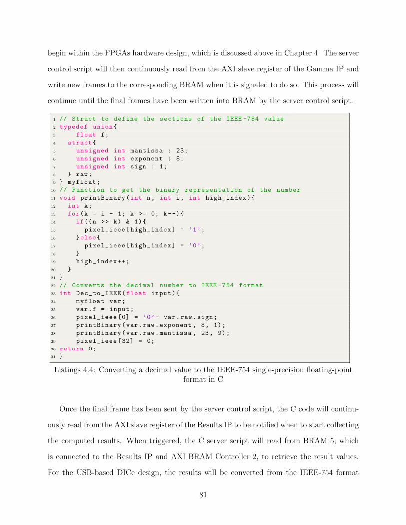
begin within the FPGAs hardware design, which is discussed above in Chapter 4. The server
control script will then continuously read from the AXI slave register of the Gamma IP and
write new frames to the corresponding BRAM when it is signaled to do so. This process will
continue until the final frames have been written into BRAM by the server control script.
1 // Struct to define the sections of the IEEE -754 value
2 typedef union{
3 float f;
4 struct{
5 unsigned int mantissa : 23;
6 unsigned int exponent : 8;
7 unsigned int sign : 1;
8 } raw;
9 } myfloat;
10 // Function to get the binary representation of the number
11 void printBinary(int n, int i, int high_index){
12 int k;
13 for(k = i - 1; k >= 0; k--){
14 if((n >> k) & 1){
15 pixel_ieee[high_index] = ’1’;
16 }else{
17 pixel_ieee[high_index] = ’0’;
18 }
19 high_index ++;
20 }
21 }
22 // Converts the decimal number to IEEE -754 format
23 int Dec_to_IEEE(float input){
24 myfloat var;
25 var.f = input;
26 pixel_ieee [0] = ’0’+ var.raw.sign;
27 printBinary(var.raw.exponent , 8, 1);
28 printBinary(var.raw.mantissa , 23, 9);
29 pixel_ieee [32] = 0;
30 return 0;
31 }
Listings 4.4: Converting a decimal value to the IEEE-754 single-precision floating-pointformat in C
Once the final frame has been sent by the server control script, the C code will continu-
ously read from the AXI slave register of the Results IP to be notified when to start collecting
the computed results. When triggered, the C server script will read from BRAM 5, which
is connected to the Results IP and AXI BRAM Controller 2, to retrieve the result values.
For the USB-based DICe design, the results will be converted from the IEEE-754 format
81

1 // Read from the image file ...
2 if(TIFFReadRGBAImage(tif , w, h, raster , 0)){
3 // Iterate through the total number of pixels
4 for(int i = 0; i < npixels; i++){
5 // Retrieve each individual pixel value from the B channel
6 int pixel = (int) TIFFGetB(raster [(( width * (height -
moveDown)) - moveRight)]);
7 // Convert the pixel , in integer form , to a float
8 pixel_float = pixel;
9 // Normalize the pixel value by dividing it by 255.0
10 Norm_pixel_float = pixel_float / 255.0;
11 // Convert the resulting decimal to IEEE -754 format
12 Dec_to_IEEE(Norm_pixel_float);
13 // Convert the resulting IEEE -754 number into a binary string
14 pixel_ieee_string = &pixel_ieee;
15 // Convert the 32-bit IEEE 754 number to a decimal
16 pixel_ieee_bin =(int)strtol(pixel_ieee_string ,(char **)NULL
,2);
17 // Write the pixels to the BRAM registers
18 if(fileNum == 1){
19 BRAM_CTRL_0_REG[i] = pixel_ieee_bin;
20 }
21 else if(fileNum == 2){
22 BRAM_CTRL_1_REG[i] = pixel_ieee_bin;
23 }
24 }
25 }
Listings 4.5: Converting individual pixels to the IEEE-754 format and writing them toBRAM in C
82

to scientific notation locally on the FPGA and locally formatted into solution files that are
saved on the USB drive. The process of converting an IEEE-754 number back to decimal is
essentially the reverse process shown in Listings 4.4 and 4.5 above. For the Ethernet-based
DICe design, the results are read from BRAM, where they are automatically inferred as
decimal values, and transmitted back to the client script on the connected host PC after
they are separated with a comma as the delimiter. A similar code block is implemented on
the client control script to convert the results back to a human-readable format and placed
into text-based solution files.
83

Chapter 5
Results
This chapter will present the reader with the results obtained from the development of
the DICe hardware accelerator. A variety of figures were obtained from different approaches
of creating the control scripts for the DICe hardware accelerator so that these methods can
be compared to one another. A breakdown of the DICe hardware design is presented that
shows the execution time as well as the resource utilization for the design. Results of the
hardware accelerators’ performance are showed that compare it to the DICe GUI. Figures
are provided that show the execution times for the varying amount of frames and subsets
during processing. Results are shown for the speeds of the Ethernet-based design as well as
the USB-based design. Lastly, the floating-point library that was developed for this work is
discussed to highlight the significance it has in the DICe hardware accelerator.
5.1 Python-Based Control Script Performance
The first implementation method to be discussed will be the use of Python for the con-
trol scripts that run on the workstation PC. Python was the first high-level programming
language that was used to develop the control scripts due to its ease of use that enabled the
quick development and testing of the functionality of these scripts. For a quick refresher,
the job of the control scripts is to retrieve the parameters data that is contained within the
user-defined Subsets.txt file, retrieve the images that are to be processed by the DICe hard-
ware design on the FPGA, and transmit all of this data to the FPGA by establishing a TCP
connection. The initial design of the control scripts implemented the conversion process of
each pixels intensity value within the image to the IEEE-754 single-precision floating-point
format. While this is no longer used for the final DICe hardware accelerator design, the
execution times of this process will be presented to showcase why moving this process to the
FPGAs ARM Cortex-A53 processor was necessary.
The first figure of results that are shown below in Figure 5.1 shows the total execution
84

time for a simple Python script to open up a single .tif image and retrieve all of its pixel
values. This process is performed and reported because it is necessary to know how long
the Python script takes to iterate through the image to obtain each pixel intensity value.
Once all of these values are obtained, they are stored in a local variable so that they may be
transmitted over Ethernet afterward. Figure 5.1 below shows that this process takes 55.447
ms to execute, which is a substantial amount of time. This reported execution time shows
the average processing time it took to retrieve all pixel values of a single image across 10
runs. The execution time of the script that is reported in this figure, along with the rest of
the high-level based scripts, will later be compared to their C-based equivalents.
Figure 5.1: A snapshot from the PCs CLI of the Python script opening a single 448x232frame and retrieving all of its pixel values
The second image that is shown in Figure 5.2 reports the processing time to retrieve the
pixel intensity values of one image and to transmit that data to the server on the FPGA
over a TCP-based Ethernet connection. Something to note at this point is that the image
size used for these results is a single 448x232 pixel size frame that is in .tif format. The
original image is approximately 154.9 KB in size. When the Python script iterates through
this image and transmits the pixel data to the FPGA, the total amount of data is 280 KB.
This increase of nearly 120 KB of data for the image data is the result of adding commas
after the pixel values so that they are separated by a delimiter. This delimiter allows the
server script running on the FPGA to separate these pixels into individual values. If the
pixels were all transmitted separately, the total processing time for transmission would be
85

longer due to the increase in the number of packets sent. If the pixel data was sent unaltered
to the FPGA, then the server script would be unaware of which pixel values are unique
because the received data would be a concatenation of all of the pixel values. Now, the
results shown in Figure 5.2 shown an image processing time (to retrieve all pixel values) of
58.415 ms and a data transfer time of 2.356 ms. The total execution time of the script is the
sum of these execution times at 60.819 ms. Again, these numbers are the averaged results
from the execution of 10 runs. While these reported results require nearly 6 ms more time to
process, it can be seen that only 2.356 ms of that time is dedicated to transferring the image
data to the FPGA. The remaining increase in processing time is from processing the original
image; these results vary for every run which is why the average of 10 runs is computed and
reported in these figures. So with this, it can be seen that the time to retrieve the pixel
intensities from the image is time-consuming while transmitting the data is not a concern.
Figure 5.2: A snapshot from the PCs CLI of the Python script opening a single 448x232frame, retrieving all of its pixel values, and transferring them to the ZCU104 FPGA via
Gigabit Ethernet
Figure 5.3 is comparable to Figure 5.1 in that both scripts open a single image and retrieve
all of the pixel intensity values. However, Figure 5.3 differs from the previous figure in that it
86

converts each pixel it receives to the IEEE-754 single-precision floating-point format before
storing it into a local variable. This was one of the original responsibilities that the control
script needed to perform. The total execution time for this process is 788.341 ms, which
is a substantial 1,421.79% increase in execution time over just retrieving the pixel values.
While Python enabled quick implementation and testing of the control scripts functionality,
this execution time was highly undesirable and needed to be resolved to successfully create
a DICe hardware accelerator. The process for converting the pixel intensities decimal value,
which ranges between 0 and 255, to the IEEE-754 single-precision floating-point format is
shown in Listing 5.1. While this algorithm computes the correctly converted values, its
processing time was slow.
Figure 5.3: A snapshot from the PCs CLI of the Python script opening a single 448x232frame, retrieving all of its pixel values, and converting them to IEEE-754 single-precision
floating-point format
The last Python-based result is shown in Figure 5.4 and shows the execution time to
retrieve the pixel intensity values from the image, convert them to the IEEE-754 format, and
transfer the data to the server on the FPGA via a TCP-based Ethernet connection. The
total execution time for this process was 758 ms, where 749.997 ms of time was dedicated
to converting the pixel values to the IEEE-754 format and the remaining 7.957 ms were for
transmitting the data to the server on the FPGA. Because the pixel intensity values have
been converted to the IEEE-754 format, they are longer in size. The resulting number is a
87

1 # Get all of the pixel values from the image
2 allPixels = list(img.getdata (0))
3 # Loop through each pixel in the image and convert to IEEE -754 format
4 for pixel in allPixels:
5 # Normalizes the pixel value by dividing it by 255
6 pixel_normalized = pixel / float (255.0)
7 # Converts each pixel to its corresponding IEEE 754 representation
8 pow = -1
9 fraction_dec = 0
10 fraction_bin = list("00000000000000000000000")
11 n = pixel_normalized
12 # Determine the sign bit
13 if pixel_normalized >= 0:
14 sign = ’0’;
15 else:
16 sign = ’1’;
17 # Compute the exponent and mantissa
18 if pixel_normalized == 0:
19 Output_bin = "00000000000000000000000"
20 else:
21 while abs(n) < 1 or abs(n) >= 2:
22 try:
23 n = pixel_normalized / (2 ** pow)
24 except ZeroDivisionError:
25 n = 0
26 pow = pow -1
27 exp_int = pow + 1 + 127
28 exp_bin_str = str(Bits(int = exp_int , length = 8).bin)
29 fraction_dec = n - 1;
30 for i in range(0, 23):
31 temp = fraction_dec * 2
32 if temp < 1:
33 fraction_bin[i] = ’0’
34 fraction_dec = temp
35 else:
36 fraction_bin[i] = ’1’
37 fraction_dec = temp - 1
38 final_fraction = "".join(fraction_bin);
39 Output_bin = str(sign) + str(exp_bin_str) + str(final_fraction)
40 # Converts each IEEE 754 binary pixel value to decimal
41 # (represents the IEEE in 32-bit binary)
42 dec = int(Output_bin , 2)
43 # Concatenate all pixel values with a comma delimiter
44 bigString += str(dec) + ’,’
Listings 5.1: Python code for retrieving pixel intensity values from the image andconverting it to the IEEE-754 single-precision floating-point format
88
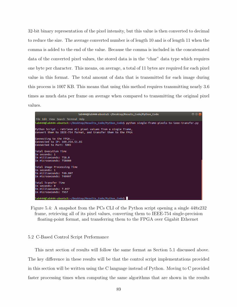
32-bit binary representation of the pixel intensity, but this value is then converted to decimal
to reduce the size. The average converted number is of length 10 and is of length 11 when the
comma is added to the end of the value. Because the comma is included in the concatenated
data of the converted pixel values, the stored data is in the “char” data type which requires
one byte per character. This means, on average, a total of 11 bytes are required for each pixel
value in this format. The total amount of data that is transmitted for each image during
this process is 1007 KB. This means that using this method requires transmitting nearly 3.6
times as much data per frame on average when compared to transmitting the original pixel
values.
Figure 5.4: A snapshot from the PCs CLI of the Python script opening a single 448x232frame, retrieving all of its pixel values, converting them to IEEE-754 single-precision
floating-point format, and transferring them to the FPGA over Gigabit Ethernet
5.2 C-Based Control Script Performance
This next section of results will follow the same format as Section 5.1 discussed above.
The key difference in these results will be that the control script implementations provided
in this section will be written using the C language instead of Python. Moving to C provided
faster processing times when computing the same algorithms that are shown in the results
89

of the previous sections. The move to C also provided an easy transition when creating the
server control script that runs on the FPGAs ARM Cortex-A53 processor. Converting the
control script from Python to C presented a few challenges. The first was that opening .tif
images was not nearly as easy and required the installation of the “libtiff” library. Strict
data types had to be created for all variables that were used and the code to convert a pixel
intensity value to the IEEE-754 format needed to be redeveloped as well. The code for the
C-based program to convert pixels to the IEEE-754 format can be seen in Listing 4.4, in
Section 4.2.2 of Chapter 4.
Figure 5.5 is the first figure of results provided for this section and shows the execution
time for the C-based script to open a single image and retrieve all of the pixel intensity values.
What is remarkable about this figure, is that the total execution time that is reported is
2.734 ms, which is significantly smaller when compared to the Python-based equivalent at
55.447 ms.
Figure 5.5: A snapshot from the PCs CLI of the C script opening a single 448x232 frameand retrieving all of its pixel values
Moving on to Figure 5.6, this figure reports the total execution time to retrieve all of the
pixel intensity values from a single frame and transmit it to the FPGA via Ethernet. The
C script uses the same socket parameters that were defined in the Python script to handle
TCP transmissions over Ethernet. The functions used to create a socket-based connection
in C were carefully evaluated to ensure that they had the same parameters that were defined
90

in the Python script. The image processing time closely resembles the results shown in the
previous figure and the total transfer time of 2.693 ms is nearly identical to the reported
time in the Python-based script of 2.356 ms.
Figure 5.6: A snapshot from the PCs CLI of the C script opening a single 448x232 frame,retrieving all of its pixel values, and transferring them to the ZCU104 FPGA via Gigabit
Ethernet
The C-based control script continues to show its processing performance capabilities with
Figure 5.7. This figure shows the total execution time to retrieve all of the pixel intensity
values from a single image and convert them to the IEEE-754 format. As reported, it
completes this task in only 20.59 ms which, when compared to the Python-based equivalent,
is over 38 times faster. The primary reason for choosing to develop the final control script
in C over Python was for this very reason. Python was beyond slow at converting pixel
intensities to their IEEE-754 format representations while the C-based script excelled at it.
Moving to the last figure of this subsection, Figure 5.8 shows the total execution time
to retrieve all pixel intensity values from a single image, convert them all to the required
IEEE-754 format, and transmit them to the server on the FPGA. The total execution time
for this process in C was 21.535 ms. When this is compared to the equivalent Python-based
91

Figure 5.7: A snapshot from the PCs CLI of the C script opening a single 448x232 frame,retrieving all of its pixel values, and converting them to IEEE-754 single-precision
floating-point format
script with a total execution time of 758 ms, it is apparent which language provides the
benefit with the C-based control script completing the same task over 35 times faster.
The consolidated results can be seen in Table 5.1. It is apparent that the C-based control
script outperforms the Python-based script in every test case provided. All of these cases are
with the control scripts implemented on a workstation PC with the following specifications:
Ubuntu 18.04 LTS, 8 GB of RAM, 251 GB of disk space, and an octa-core Intel i7-4770
CPU at 3.40 GHz. It should be noted that multiprocessing was not used for any of the test
cases for these control scripts. The average Ethernet transfer speeds from these tests will be
reported below in Section 5.4.
With all previous results pointing to the C-based control script running on the PC to
be the superior method, the code developed for the control script was slightly modified to
run on the FPGA for some additional testing. The results of Figure 5.9 and Figure 5.10
assume the same parameters of the previous control scripts in that the image data is readily
available in memory. This was tested by loading the sample image into the USB 3.0 drive
so that the FPGA could access it. Figure 5.9 shows the modified control script running on
the ZCU104 FPGAs ARM Cortex-A53 processor using PetaLinux. The script retrieves the
sample image in the USB drive, retrieves each pixel intensity value from the image, and
92

Figure 5.8: A snapshot from the PCs CLI of the C script opening a single 448x232 frame,retrieving all of its pixel values, converting them to IEEE-754 single-precision floating-point
format, and transferring them to the ZCU104 FPGA via Gigabit Ethernet
Figure 5.9: A snapshot from the FPGAs CLI of the C script opening a single 448x232frame and retrieving all of its pixel values
stores the data in a local variable. The reported time for this process to execute was 15.92
ms which is slower than the performance achieved when running on the PC. Figure 5.10
93

Table 5.1: Performance comparisons between the Python-based and C-based control scripts
Control Script Performance Comparisons (ms)
LanguageIEEE
ConversionTime
TransferTime
TotalExecution
TimePython 0 0 55.447
C 0 0 2.734Python 0 2.356 60.819
C 0 0.22 2.917Python 788.315 0 788.341
C 20.593 0 20.722Python 749.997 7.957 758
C 21.314 0.218 21.535
performs the same functions except converts each pixel to the IEEE-754 format. The total
execution time for this was 160.856 ms which is much slower than the performance achieved
on the PC. A major factor in this difference in performance is that the FPGAs processor
runs at a maximum speed of 1.3 GHz while the processor on the PC runs at 3.40 GHz.
Figure 5.10: A snapshot from the FPGAs CLI of the C script opening a single 448x232frame, retrieving all of its pixel values, and converting them to IEEE-754 single-precision
floating-point format
94
5.3 USB-based Design
One of the main purposes for the work that is presented in this thesis is to provide the
users of the DICe hardware accelerator with more than one way to access frame data when
running the application. By using the ZCU104 FPGA, it is possible to implement the USB
3.0 port as a method to access this data. This is beneficial for the users of DICe who already
have all of the frame data they wish to operate on ready within some memory medium. If
they copy this data to a USB-based device from the start of data collection, they can receive
significant improvements in correlation time due to the data being ready for the FPGA to
access. If the user writes the frame data to a directory within the workstation PC, they will
incur the delay of copying the large amounts of frame data over to a USB-based device before
execution on the FPGA. The USB 3.0 flash drive that was used was formatted to fat32 for
these results. This is because fat32 provided the best results in terms of reading and writing
speeds. Other formats for the USB drive were attempted, such as ext4 and NTFS, but they
did not outperform the results obtained from using the fat32 format.
Using the USB 3.0 port to access frame data is one of the best features that the user
has available to them with the DICe hardware accelerator. This is because of the incredibly
fast read speeds that this port provides the user to access the frame data. By using the
CLI that PetaLinux provides, it was possible to run accurate memory read and write tests
with the USB using the f3 package [46]. Figure 5.11 shows the read speeds from the USB
3.0 drive that is achieved on the ZCU104 FPGA. An incredible 211.29 MBps speeds were
achieved for reading from the USB drive; this is equivalent to 1690.32 Mbps, or 1.69032 Gbps
of reading speed. This is a phenomenal result in that this is the fastest method available
to transfer large amounts of frame data to the FPGA. While Ethernet transmission speeds
will be reported in the next section, the ZCU104 has a max Ethernet throughput of 1000
Mbps or 1 Gbps. The reason it is called Gigabit Ethernet is that it is limited to transmit
a Gigabit’s worth of data every second. This means that the read speeds from the USB
3.0 port are the best option for the users to transmit frame data because the frame data
95
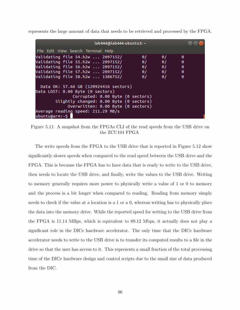
represents the large amount of data that needs to be retrieved and processed by the FPGA.
Figure 5.11: A snapshot from the FPGAs CLI of the read speeds from the USB drive onthe ZCU104 FPGA
The write speeds from the FPGA to the USB drive that is reported in Figure 5.12 show
significantly slower speeds when compared to the read speed between the USB drive and the
FPGA. This is because the FPGA has to have data that is ready to write to the USB drive,
then needs to locate the USB drive, and finally, write the values to the USB drive. Writing
to memory generally requires more power to physically write a value of 1 or 0 to memory
and the process is a bit longer when compared to reading. Reading from memory simply
needs to check if the value at a location is a 1 or a 0, whereas writing has to physically place
the data into the memory drive. While the reported speed for writing to the USB drive from
the FPGA is 11.14 MBps, which is equivalent to 89.12 Mbps, it actually does not play a
significant role in the DICe hardware accelerator. The only time that the DICe hardware
accelerator needs to write to the USB drive is to transfer its computed results to a file in the
drive so that the user has access to it. This represents a small fraction of the total processing
time of the DICe hardware design and control scripts due to the small size of data produced
from the DIC.
96

Figure 5.12: A snapshot from the FPGAs CLI of the write speeds from the USB drive onthe ZCU104 FPGA
5.4 Ethernet-Based Design
The use of an Ethernet connection was the foundation for transferring frame data to the
FPGA so that the DICe hardware accelerator could execute. This project started with the
use of the 7 Series Xilinx FPGAs, specifically the Kintex-7 and the Virtex-7, which only
had Ethernet ports available to them as the best means to transfer large amounts of data.
Further on throughout the development process, it was seen that the used hardware design
to enable Ethernet on the Virtex-7 FPGA was not achievable. While an initial hardware
design was achieved when using the Kintex-7 FPGA, only a maximum Ethernet throughput
of 56 Mbps was attained. This left a huge void in the development process because there
was not a suitable way to transfer the potentially thousands of frames needed for DIC to the
FPGA.
When the ZCU104 was introduced to the development of this project, the throughput of
the Ethernet connection improved by a few orders of magnitude in under a week. The use of
the PetaLinux tools enabled a simplified approach to enable Gigabit Ethernet on the ZCU104
FPGA. With this, substantially improved Ethernet speeds were accomplished that allowed
for a practical second method of transferring frame data to the FPGA. Figure 5.13 shows a
screenshot from the host PCs CLI when transmitting data to the FPGA. When transferring
97

1.1 GB of data to the FPGA from the host PC, an average speed of 941 Mbps was achieved.
This is over a 16 times performance increase when compared to the speeds achieved when
using the Kintex-7. For the first time when using the ZCU104 FPGA, transmitting thousands
of frames over Ethernet was a viable possibility.
Figure 5.13: A snapshot from the PCs CLI of the Ethernet network speed from the PC tothe ZCU104 FPGA
As shown in Figure 5.14, the Ethernet speeds when transmitting data from the FPGA
to the PC are nearly equivalent. The figure is a screenshot from the FPGAs CLI when
transmitting the same 1.1 GB of data to the PC over a TCP-based Ethernet connection.
The result of this is a bandwidth speed of 942 Mbps which is only slightly faster than
the results shown in Figure 5.13. This slight difference is simply caused by executing the
programs at different times as they both varied by about 1 Mbps of speed when ran multiple
times. This is a significant result that the FPGA has achieved because it results in reduced
time to transfer across all of the solution data to the PC. However, the bulk of the data that
needs to be transmitted is the frame data from the PC to the FPGA. While 941 Mbps is
certainly an outstanding throughput, it does not compare to the USB read speeds that are
nearly twice as fast at a throughput of 1.7 Gbps. While this comparison seems to show USB
as the optimal choice when running the DICe hardware accelerator, a user must consider
a variety of factors. To use the USB drive as the fastest method of providing the FPGA
with frame data, all of the data needs to be complete and readily available on the USB
drive. There exists a lot of circumstances where the user of DICe would need to copy all of
98

the data over to a USB-based device, which takes time. The data produced by the camera
recording the frames could still be processing which means that the USB method cannot be
used. Whereas with the Ethernet-based design, the frames could be streamed over to the
FPGA as they are available which could reduce the overall amount of time performing DIC.
Figure 5.14: A snapshot from the FPGAs CLI of the Ethernet network speed from theZCU104 FPGA to the PC
Due to the extensive reporting on the previously used FPGAs for this project, it seemed
imperative to include a side-by-side comparison of the Ethernet speeds of the multiple FPGAs
used. Table 5.2 shows all of the FPGAs that were used during the development of this
project and how they compare in Ethernet throughput and achieved Ethernet throughput.
The primary takeaway from this table, and as previously mentioned in this thesis, is that
the Zynq UltraScale+ MPSoC FPGA contains a quad-core ARM Cortex-A53 hard processor
and a physical IP for the Ethernet interface. The 7 Series FPGAs in this table both use the
MicroBlaze soft processor and contain only HDL-based IP that is to be implemented within
the hardware design of the application to enable Ethernet connectivity. Both of these factors
proved to be severe limitations when attempting to establish Gigabit Ethernet connectivity
between the FPGAs and the host PC.
99

Table 5.2: Ethernet performance comparisons between FPGAs
Ethernet Speeds (Mbps)
FPGA Processor Ethernet IP InterfaceTheoretical
SpeedActualSpeed
Virtex-7(VC707)
MicroBlazeAXI Ethernet
SubsystemSGMII 1000 X
Kintex-7(KC705)
MicroBlazeAXI Ethernet
LiteMII 1000 56
ZynqUltraScale+
MPSoC[ZCU104]
ARMCortex-A53
PHY RGMII 1000 950
5.5 DICe Hardware Design Performance
The most significant development that went into the DICe hardware accelerator was
with the hardware design. The hardware design that runs within the ZCU104 FPGAs fabric
is the most critical component of this project because it is responsible for performing the
digital image correlation algorithms that are present in DICe. The design used nearly all of
the available BRAM on the FPGA and a total of 7,292 lines of Verilog code were written
between all of the custom IPs. A bar graph of the resource utilization on the ZCU104 FPGA
after programming it with the DICe hardware design bitstream is provided in Figure 5.15.
Table 5.3: The available and utilized resources for the DICe hardware design on theZCU104 FPGA
Resource Utilization Available Utilization %LUT 37,499 230,400 16.28LUTRAM 2,787 101,760 2.74FF 33,362 460,800 7.24BRAM 279 312 89.42URAM 96 96 100.00DSP 11 1,728 0.64IO 3 360 0.83BUFG 4 544 0.74MMCM 1 8 12.50
100

Figure 5.15: A graph of the resource utilization for the DICe hardware design on theZCU104 FPGA
A more detailed breakdown of the utilized resource of the FPGA can be viewed in Table
5.3. This table highlights the significance of the SRAM-based memory for the DICe hardware
design with 100% URAM utilization and 89.42% BRAM utilization. Without a doubt,
working with these memory constraints was the most critical challenge that was faced when
developing the DICe hardware design. It can be seen that the other resources within the
FPGAs fabric did not come close to being considered critical. The next most used resource in
the design was the LUTs which only comes to 16.28% of the total LUTs available. DSP blocks
were scarcely used, but were implemented in the floating-point library that was developed
for this project. The total DSP utilization for each function can be seen below in Section
5.6.
Table 5.4 shows two examples of the DICe hardware accelerator in direct comparison
to the performance of the DICe GUI. Both the FPGA and DICe GUI were subjected to
the same parameters in regards to image size, subset size, and subset count. To make the
comparison even, to truly expose the hardware acceleration that is possible when targeting
101

the FPGA, the images and subsets were pre-loaded into memory so that they would have
fair access times when compared to the DICe GUI that accesses all of its data locally from
the PCs internal memory. With this, a significant speedup is obtained from both results
that are running within the ZCU104 FPGA. These results show that the DICe hardware
accelerator achieved at its core design with the ability to out perform the DICe GUI. The
looming factor of these results however, is that the data was pre-loaded into the FPGAs
memory. This is temporary measure that effectively deviated around the larger problem
that this thesis attempts to express in that the FPGA cannot have a significant amount of
image data pre-loaded onto it; there must be some sort of method for data to be transferred
to the FPGA to perform consistent digital image correlation on a large source of data. Note
that the results displayed in Table 5.4 only show the execution time for two frames that have
undergone DIC. These results are simply presented to show the raw difference in execution
times between the DICe GUI and the newly developed hardware accelerator for a base case.
Table 5.4: Performance comparisons between DICe execution methods
DICe Performance Comparisons (ms)Test Case DICe GUI DICe FPGA Speedup2 frames (64x48), 1 subset (3x3) 16 2.5 6.4x2 frames (448x232), 1 subset (21x21) 116 14 8.286x
Because the results shown previously in Table 5.4 only perform DIC on a single run
consisting of two frames, it does not factor in the full impact of the DIC algorithms when
subsets are applied and being correlated for each round of frames that are presented. This
presents a significant computational overhead due to the algorithms in the Gamma IP work-
ing to their fullest extent. The graph provided in Figure 5.16 shows the results of a more
real-world example when the DICe hardware accelerator operates on a range of frames and
has to consider subsets in its correlation routines. The Ethernet-based method was used for
these tests to show the worst-case scenario when running the DICe hardware accelerator.
The results of these runs, that operate on 10 to 40,000 frames and 1 to 7 subsets of varying
102

sizes, accurately displays the computational overhead that is incurred when the correlation
routines have to factor in more frames and subsets. While the previously shown results for
DIC between two frames with one subset of size 21x21 pixels show a total execution time of
14 ms, this time is significantly impacted by the fact the correlation routines do not have
to compute the change in frames and subsets for more rounds of DIC. Up until the 10,000
frame marker in the graph, the results for all runs are logarithmic which is a good sign that
shows it is possible to achieve better performance through modifications to the hardware
design.
Figure 5.16: A line graph that shows the total execution time of the DICe hardwareaccelerator in reference to the number of frames, the number of subsets, and the size of the
subsets
The bar graph displayed in Figure 5.17 uses the same test runs as the previous graph, but
it emphasizes the total execution time required for each frame. What this graph presents
well is that as the subset size increases and as the number of subsets increase, the processing
103

time increases with it. The jump from a 21x21 pixel sized subset to a 41x41 pixel sized
subset is a four times increase in area to perform correlation over. At the core of the DICe
algorithms that were implemented within the hardware design, they focus on tracking the
differences between each subset from frame to frame. So as the number of subsets increases,
more iterations are required within the design to correlate the subsets. As the size of the
subset is increased, the more area and pixels the Subset Coordinates IP, Gradients IP, and
Gamma IP are required to iterate over to accurately compute the distinctions between each
run.
Figure 5.17: A bar graph that shows the total execution time per frame of the DICehardware accelerator in reference to the number of frames, the number of subsets, and the
size of the subsets
5.6 Floating-Point Library Performance
The last major contribution that this thesis presents is a novel library of FSM-based
floating-point arithmetic functions on FPGAs [21]. This library was developed specifically
for this project due to the required functions that the DICe algorithms implemented. Pre-
vious works have created similar libraries for arithmetic operations on FPGAs, but they
104

either utilized too much of the FPGAs BRAM resources or they were based on a pipelined
architecture. Each of these cases was unsuitable for the DICe hardware accelerator because
the algorithms are heavily sequential and the majority of the FPGAs BRAM was used for
frame and results buffering. This work was recognized at the 2019 ReConFig conference as
a long paper and has since been published in the IEEEXplore catalog.
Each function created is based on an FSM architecture that allows for specific operations
to happen in individual states that take one clock cycle to execute. Due to the sequential
nature of the DICe algorithms, the goal for each of these functions was to have them execute
as fast as possible so that another value could be processed immediately after. This differs
from a pipelined architecture because in a pipelined system a value would be read into the
first state and by the time the first state is finished executing then a new value would proceed
to the first state while the second state operates on the first value. This architecture was
not ideal because the DICe algorithms contain many dependencies, values that depend on
previously computed values. Figure 5.18 shows a simple flow diagram that traces through the
states of the addition function. Similar diagrams can be found in [21] for the multiplication
and division functions along with resource utilization of each function within the library.
The results and the development of this library will not be reported extensively here
because they can be found in the published paper [21]. The last set of results that will
be presented in this library are shown in Figure 5.19. These consolidated bar graphs show
how the newly developed FSM-based library compares to the related works in the research
area of floating-point operations on FPGAs. Only the four basic arithmetic functions (ad-
dition, subtraction, multiplication, and division) are shown in these graphs that compare
the total delay, number of LUTs, and number of FFs. While this library does include a few
trigonometric functions (sine, cosine, arcsine, and arccosine), they are not compared to any
other related works simply because they were hard to find. Even the Xilinx Floating-Point
Operator IP does not support floating-point trigonometric operations. This is another one
of the leading factors that led to the development of this library, to assure that we had all of
105

Figure 5.18: A block diagram of the addition function in the floating-point library
the required functions to properly implement the DICe algorithms within the hardware de-
sign. These graphs accurately show how well the FSM-based library compares to the related
works in terms of performance and resources. The development of this library was one of the
primary reasons the DICe hardware accelerator had success. Many of the algorithms found
within DICe require a large number of mathematical operations that execute repetitively,
so creating functions to support these sequential operations was key to the success of the
application.
106

Figure 5.19: Comparison of the proposed and the previous basic floating-point arithmeticfunctions (a) Delay (b) LUTs (c) FFs
107

Chapter 6
Discussion
This section provides a discussion on some topics that were not covered in previous
chapters as well as potential future works. This project was complex and time-consuming to
develop due to the density of the DICe source code, the learning curve required to develop
hardware-based applications, and understanding image processing. The DICe hardware
accelerator evolved many times as more knowledge was gained from the DICe source code
and the hardware that was used. The biggest evolution of this project, and one this thesis
highlights below in Section 6.1, is the use of the PetaLinux tools to create a Linux-based
kernel on the ZCU104 FPGA. Using PetaLinux drastically changed the way this project was
approached and brought several significant improvements to the design and performance of
the application. The previous method of using the lwIP TCP/IP stack to implement the
Ethernet interface was clunky, slow, and error-prone when programmed onto the MicroBlaze
soft-processor. The complexities of this project also led to a variety of challenges that will be
discussed below in Section 6.2. From working with 32-bit floating-point numbers in Python-
based and C-based control scripts to scaling up the design to support multiple frames and
subsets when migrating between the KC705, VC707, and ZCU104 FPGAs, this project had
many complex problems that needed to be solved before the application design progressed.
6.1 PetaLinux vs. lwIP
When development for this project started the only two FPGAs that were available were
the Kintex-7 (KC705) and the Virtex-7 (VC707). These FPGAs do not contain a PS side
like the ZCU104 board does; this means no hard processors, GPUs, or hard IP [8–10]. The
KC705 and VC707 were challenging to work with because every I/O port that was needed
for use had to be manually setup and configured within Vivado before synthesis and writing
the bitstream. These FPGAs leverage a soft processor known as the MicroBlaze to act as
the central control for a design. With these FPGAs, work on the core of the hardware
108

design was able to continue at a steady pace. The biggest set back that was faced with
these boards was designing a functioning hardware design that supported Ethernet I/O. A
working Ethernet design was finally established after months of problem-solving, but only
on the KC705 FPGA. Once this step was achieved, the next step was determining how to
interface with the Ethernet port. This is where the lwIP stack comes into play.
The lwIP stack is an open-source TCP/IP stack that is designed for use with embedded
systems [57–59]. Many manufactures, like Xilinx, use the lwIP stack for their systems to
provide a full TCP/IP stack that enables Ethernet communications while reducing the num-
ber of resources that standard stacks use. At its start, this project utilized the lwIP stack
because it was available as an example in the Vivado SDK and also because it was one of
two methods to provide a functioning TCP/IP stack to the FPGA. The Vivado SDK tool
provided a method to target the MicroBlaze soft processor with C code to implement the
lwIP stack. This provided a working template that could then be modified to suit the needs
of this application. Using the lwIP stack started with a simple echo server example that
communicated with a Python client on the workstation PC.
Once the fundamentals of this code were fully understood, both scripts were then modified
to handle the transferring of images. The PC-side Python script was responsible for accessing
the images, transmitting the pixel values over Ethernet to the FPGA-based server, and
handling the handshaking between the PC and FPGA to delegate when new frames should
be sent and when results were being received. The FPGA-based server was responsible for
receiving every pixel value for each image, converting the pixel values to 32-bit IEEE-754
single-precision floating-point format [22], and writing these values to the corresponding
BRAM so that the hardware design could act on the data. The FPGA-based server-side was
also responsible for generating start and stop signals to individual custom IPs to coordinate
the image processing when new frames were received. Lastly, the FPGA-based server-side
would be notified from the custom IPs when the image correlation was finished so that it
could read the computed results from the BRAM and send them back to the workstation
109

PC for formatting.
The process of using the lwIP stack to transmit data between the PC and the FPGA
worked, but poorly. After extensive modifications to the lwIP server parameters that compile
into the Board Support Package (BSP) file, the maximum Ethernet speed that was achieved
using the Kintex-7 FPGA was 56 Mbps. While disappointingly slow when compared to the
maximum possible Ethernet speed this board is capable of at 1000 Mbps, it was all that was
available at the time for this project. An extensive amount of work went into modifying the
hardware design for the soft Ethernet IPs and modifying the lwIP settings that ultimately
configured the Ethernet interface that was used. On top of the slow Ethernet speeds, the
modified C file that represented the server on the FPGA was problematic in various ways.
Initially, the C file provided the infrastructure that was needed to establish communication
via Ethernet between the PC and the FPGA. Upon further development, it became a barrier
rather than an access point for our data. When a high volume of frame data was received by
the server, it had a hard time keeping up with processing. This is because the MicroBlaze soft
processor was responsible for running the lwIP stack to receive the frame data, converting all
103,936 pixels from every image to 32-bit IEEE-754 single-precision floating-point format,
writing the data to BRAM, and starting on the next frame. To simply put it, the MicroBlaze
core was over-exploited due to its ability to run C code.
The complication with the MicroBlaze processor led to a handful of issues that were
experienced on the server-side of the FPGA. The most common theme was timing issues.
The C script ran into timing issues when trying to receive frame data, convert pixels to write
to BRAM, and communicating with the custom IPs. The clue that led to the discovery of
the MicroBlaze processor being overused was that by adding simple print statements to the
C script, that would print out to the connected serial port on the PC, seemed to resolve a
variety of timing issues. This is because a standard print statement takes a long time. After
all, the code needs to process and after it has to display the output to the user through
the terminal. By adding these print statements to the C script during times of intensive
110

processing, it essentially added a time delay to the program that allowed the MicroBlaze
processor to catch up on its processing. However, by adding these time delays to one of
the primary control scripts, the overall computation time for the image correlation was
drastically increased.
Of the many issues faced with the lwIP, the biggest barrier that was faced was the process
of converting the individual pixels in an image to the IEEE-754 single-precision floating-point
format. Originally, this computationally intensive process was performed on the workstation
PC with the Python client script. Python was used because it is a great language for quick
scripting and testing of programs. With a handful of lines of code, the Python script was
able to open a .tif image, iterate through each pixel in the image, and convert each one
to the IEEE-754 single-precision floating-point format to send to the FPGA-based server.
However, this code effectively turned a maximum three-digit number into a 32 digit number,
which in turn is approximately 10.6 times more data to transfer to the FPGA per image.
A temporary solution was to convert this 32-bit binary number into a decimal number. For
example, if a pixel value is 100 (pixel values range between 0 and 255), it then needs to
be normalized by dividing the pixel value by 255 which equals 0.392156863 in this case.
This number, 0.392156863, when converted to the IEEE-754 single-precision floating-point
format, is equal to the following 32-bit number “00111110110010001100100011001001”.
Now, this binary number when converted to decimal equals 1,053,345,993. The difference
here is that the 32-bit binary number takes an entire byte for each digit which means that
it is equal to 32 bytes that are transmitted per pixel because they are sent using the “char”
datatype so the required commas to separate them can be added. When the 32-bit binary
number is converted into a decimal number it only requires a maximum of 10 digits which
is equal to 10 bytes (each “char” is a byte) of data to be transferred per pixel. When the
decimal number of 1,053,345,993 is transferred to the FPGA and written into BRAM, which
is composed of an array of 32-bit registers, it is automatically represented in its binary format
which is the original 32-bit IEEE-754 single-precision floating-point format that is needed
111

of “00111110110010001100100011001001”. This method of transmitting a decimal number,
that ultimately represents a 32-bit binary number, uses approximately 3.2 times more data
per pixel than sending the original three-digit pixel value. While this is an increase in the
amount of data sent, it relieves the MicroBlaze soft processor of having to convert each pixel
value for each image it receives. This trade-off ultimately pushed more of the processing
load onto the PC that transmits the image data but allowed the MicroBlaze processor to
execute its remaining tasks flawlessly. Of course, this issue is bigger when realizing that the
maximum transmission rate of the Ethernet cable was 56 Mbps.
When taking a step back from this method, it was obvious that the DICe hardware
accelerator would not be much of an accelerator at all. While the image correlation time was
improved with the hardware design that was programmed into the FPGAs fabric, the time
required to pre-process images and transmit them to the KC705 proved to be too costly.
At this point, the idea of using the USB port was never considered due to the high cost in
engineering time it took to develop a working Ethernet port and because neither the Kintex-
7 or the Virtex-7 had USB ports that were capable of the USB 2.0 or 3.0 standards. After
detailing the list of problems that were faced during the development process in a formal
report, the proposed problem and solution were relatively simple. The FPGAs used for this
period of development were unsuitable for the task that was presented and the solution was
to take our existing design and target a new FPGA that could meet the requirements for
this project.
Enter the purchase of the Zynq UltraScale+ MPSoC (ZCU104) FPGA from Xilinx. This
FPGA came equipped with 1 Gbps Ethernet, USB 3.0, a quad-core ARM Cortex-A53 pro-
cessor, a dual-core ARM Cortex-R5 real-time processor, and an ARM Mali-400 MP2 GPU
[8]. The ZCU104, when compared to the KC705, has twice as much BRAM, twice as many
Digital Signal Processing (DSP) blocks, and 1.546 times as many logic cells [8, 10]. To sim-
ply put it, the ZCU104 FPGA blew the previously used FPGAs out of the water in terms
of capability and available resources. Eager to put this new equipment to use, the original
112

Verilog-based DICe hardware design was then minimally modified to target the new FPGA
and programmed to do so. With so many new capabilities, the next few weeks were spent
on researching and understanding exactly what this FPGA was capable of so that the DICe
design could maximize this potential.
The first step was to evaluate the I/O ports in terms of data access to the images that
needed to be processed. The ZCU104 immediately provided two ports, USB 3.0 and Gigabit
Ethernet, both of which are capable of the data transmission this project required. Both
options were explored extensively before the decision was made to develop a design for both.
The reasoning behind this is that the ZCU104 FPGA did not require extensive hardware
designs in the FPGA fabric to access these I/O ports. The ZCU104 has Physical (PHY) IP on
the board that gives the ARM processors direct access to these ports. This hardware-based
approach was a significant advantage over the KC705 and VC707 where the I/O ports needed
to be manually configured with soft IP within the hardware design. While the decision to
use both I/O ports seems counterproductive given that USB 3.0 can transmit at speeds of 5
Gbps and the Gigabit Ethernet port is only capable of 1 Gbps, both options were valuable in
terms of the users at Honeywell who oversaw the original statement of work. They reasoned
that sometimes cameras are in-use and need to instantly offload images for processing via
Ethernet to get results as quickly as possible. Other times, the cameras record over a long
duration and the image data collected is stored within some memory medium, such as an
external hard drive.
The second step was to determine what software intervention would be needed to access
the memory on the FPGA so that it could successfully be written to and read from, and
how to properly access the USB and Ethernet I/O ports. After a short amount of time,
the answer was glaringly obvious that the solution was to use PetaLinux. PetaLinux is a
tool provided by Xilinx to deploy Linux-based solutions on its FPGAs [11, 12, 28]. The
tool provides the infrastructure to deploy a CLI, application templates, device drivers, a
variety of libraries, and a bootable system image on their FPGAs. Xilinx provides plenty of
113

documentation on how to use this tool to get the ZCU104 FPGA to boot with a Linux-based
kernel. The kernel of choice for this project was Ubuntu 18.04 LTS because of its familiarity.
In under a week, the SD card was prepped with the bootable image and Linux-kernel to
run on the FPGA. This tool immediately provided the drivers to access the USB 3.0 and
Gigabit Ethernet I/O ports. A problem that previously took months of work and effort to
develop was setup and running in a fraction of the time. Testing the Ethernet port im-
mediately yielded increased speeds up 950 Mbps, nearly 17 times more throughput when
compared to the speeds achieved on the KC705. The kernel allowed for the installation of
libraries and compilers to configure the ARM processor to compile and run C code. This
enabled the deployment of the C control scripts locally on the FPGA whereas previously
the control scripts were deployed on the workstation PC and had to transmit a variety of
acknowledgment signals to the FPGA to proceed with processing. The quad-core ARM
Cortex-A53 was leveraged to its fullest extent by creating a C script that utilized multipro-
cessing to pre-process frames before they needed to be written to BRAM. The struggle to
access the FPGAs memory was significantly reduced by using a C function called mmap to
locate and access available memory in the hardware design.
The PetaLinux tool provided every feature, library, and mechanism that was needed
to fully utilize the hardware on the ZCU104 FPGA in a short amount of time. Low-level
hardware designs that were previously needed to activate these features suddenly turned into
a high-level software code that was far more familiar. Development and testing time was
drastically reduced by the ability to locally compile and run C code on the FPGA without
the need to resynthesize and reprogram the FPGA. With the functioning hardware design
already programmed into the FPGA fabric and the ARM processor booting up the Ubuntu
kernel that is accessed through the serial port with the CLI, the time to test and deploy
changes to the high-level control scripts running on the ARM processor were minuscule.
The drivers needed to access the Ethernet and USB ports were enabled with the simple
click of a button, literally. Ultimately, the move to the Zynq UltraScale+ MPSoC FPGA
114

unlocked a plethora of features and abilities that were not previously available. In a short
amount of time, more progress was accomplished with the deployment and testing of the
DICe hardware design than was in months of work with the KC705 or VC707 FPGAs. The
ZCU104 FPGA coupled with the PetaLinux tool provided a platform that has significantly
improved the quality of the work presented in this thesis.
6.2 Challenges
When creating the DICe hardware accelerator a variety of challenges were experienced
which this section hopes to expand on. The first challenge was dissecting the DICe source
code, which is composed of nearly 100 C++ files. Navigating these files and their order of
execution was a massive task to undertake. The code needed to be executed so that it was
possible to trace through its execution to track down key functions. This process alone took
weeks of analysis to determine which functions were called and when. To successfully trace
through the code, the DICe GUI could not be used and the DICe source code needed to be
compiled from scratch. This in itself was a difficult task due to the minimal documentation
provided on the topic and the old operating systems used to originally build the source code.
Dozens of library packages were required to be installed on the OS of the host PC. Even
with this accomplished, using debuggers and step-through methods to analyze the code only
raised more questions than were answered. This challenge was compounded by the fact
that the DICe source code is updated monthly. Only after working closely with the lead
developer of DICe, Dan Turner of Sandia National Laboratories were the key functions of
DICe revealed. The code consisted of the following functions to port over to Verilog: com-
puteUpdateFast(), initial guess(), initialize guess 4(), initialize(), interpolate bilinear(), in-
terpolate grad x bilinear(), interpolate grad y bilinear(), gamma (), mean(), residuals aff(),
map to u v theta aff(), map aff(), and test for convergence aff() [6]. The details of these
implemented functions are explained in Section 4.1.9.
The next challenge to solve was how to efficiently transfer data across the developed
115

system. The original problem of creating the DICe hardware accelerator was how to deal
with the vast amount of data that is produced from the high-speed cameras that are needed
to be processed. The only sensible option for transferring the frame data to the FPGA was
by using a Gigabit Ethernet connection between the host PC that stores the data and the
FPGA for processing. This problem in itself took months of development to begin to transfer
data over Ethernet at all. Three variations of Xilinx FPGAs were used with only the ZCU104
board providing the necessary speeds to transmit such a high volume of data. Ethernet was
successful on the KC705 FPGA, but only up to a speed of 56 Mbps which was far too slow.
Only once the option of using the ZCU104 FPGA was available was using USB 3.0 to transfer
data considered. This thesis explores the differences of the DICe hardware accelerator in
terms of the USB-based and Gigabit Ethernet-based DICe designs. Even once Ethernet
communication was established, it was not an easy process to unlock its full potential. The
lwIP echo server provided by the Vivado SDK enabled the use of Ethernet but, after countless
modifications over months of work, the Gigabit Ethernet was never achieved. Only once the
option of using the PetaLinux tools was explored was Gigabit Ethernet available to the
FPGA, along with USB 3.0 which previously was completely unavailable. Once the primary
method of transferring data to the FPGA was implemented, it still left the challenge of how
to transfer data from the FPGAs PS side to the PL side. The data received via the I/O
ports required the use of the FPGAs provided processor. The core of the DICe hardware
accelerator lived in the FPGAs PL side. To connect these two sides, two primary methods
were used. The first was the implementation of the AXI slave registers within each custom
IP developed within the hardware design. These registers were provided addresses from
the AXI bus interface within the systems hardware design which meant that the values in
those registers, which could be written to from the IPs themselves, could also be read and
written too from the control scripts. The second method was with the control scripts’ ability
to leverage the “mmap” function in C to write to available address space defined by the
Linux-based kernel.
116

Once the challenge of system-wide communication was established, another one presented
itself. With direct communication between the FPGAs PS and PL side now available, how
the DICe application would resume processing after the first correlation has started became
a consideration. This execution flow required modifications within the hardware design of
every individual custom-built IPs and to the software designs that ran in the client and server
control scripts. Several acknowledgment signals were programmed into both the software and
hardware designs of the application to notify the FPGAs PS and PL sides that another image
should be sent and written to BRAM, when an IP should start and stop its execution, and
when the correlation was finished for all provided frames. The implementation of these
acknowledgment signals was time-consuming to perfect based on the time it takes to finish
a round of image correlation, to send a frame to the FPGA, or to convert the frame to
the IEEE-754 format. With this problem resolved through extensive development, some
problems that are inherent to the DICe software were unable to be completed. One of such
problems was to give users the ability to place subsets on the frame from a GUI. Currently,
all of the subset definitions need to be defined in the Subsets.txt file for them to be applied
to the image correlation routines. However, it is difficult for users to look at an image and
inherently know that a subset needs to be placed at a given X and Y pixel-based center
point of size Z. This problem was overlooked in the short-term development of the DICe
hardware accelerator because users can still work with the DICe GUI to provide them with
subset definitions.
Lastly, the most significant challenge faced during the development of the DICe hardware
accelerator was the limited amount of BRAM resources on all FPGAs used for this project.
BRAM was by far the most crucial resource in the DICe hardware design because each
BRAM block is responsible for buffering the frame data and the computed data for the
gradients and subsets of an image. Developing around this constraint resulted in a 448x232
sized frame to be the largest image size eligible to be processed. The consequence of this
was the DICe hardware accelerator processing images four times smaller than the required
117

image size of 896x464 that was defined in the statement of work for this project. While the
DRAM resource was abundantly available, the reading and writing access times to DRAM
proved to be too slow to keep up with the hardware accelerator which resulted in timing
faults.
6.3 Future Work
This project has many reasons to explore future work due to how dense and complex the
source code for DICe is. The first avenue to pursue would be to develop the DICe hardware
accelerator such that it retains all of the features this GUI has. Based on the requirements
this project was given, the DICe hardware accelerator that was developed for this project
only runs one analysis mode that focuses on tracking. The DICe GUI has two other analysis
modes that could be explored for the hardware-accelerated design. These analysis modes
are subset-based full-field and global. Paired with these analysis modes are the additional
optimization and correlation methods that come in simplex and robust. These analysis
modes were not developed into the DICe hardware accelerator because they were unused by
Honeywell that provided us with a statement of work for development. Their sole focus was
on the implementation of the tracking analysis mode which is what this project uses.
There exist several features that DICe is capable of but that are not implemented in this
work. The DICe GUI supports image obstructions while this implementation does not. This
feature allows the user to select regions of the image that are obstructing the movement
within the frame. For example, a frame may have a component such as a gear that spins,
but a metal mounting rack for the gear could cover up a section of the frame that blocks
a portion of the spinning gear. This feature allows the user to get more precise results;
an example of this feature is shown in Figure 6.1. Another feature that could be further
developed as future work would be the subsets. Currently, the design explained in this work
only supports circular and square subset shapes. The DICe GUI allows the user to view an
image and create their subset shape that is uniquely tailored to the content in the frame. The
118

subsets could also be improved to support a greater quantity and a larger size. Currently,
this design only allows for a max subset size of 41x41 pixels and a max number of 14 subsets,
these were based on the given requirements.
Figure 6.1: A graphical representation of an obstruction within the frames in DICe [6]
One of the given requirements that were unmet for this project was the size of the
images used. The DICe design in this work supports a frame of the size 448x232 pixels
but needed to support a frame size of 896x464 pixels. This means that the DICe hardware
accelerator only supports an image size that is one-fourth the size of the size specified in
the requirements. The reason for this shortcoming was simply due to the lack of BRAM
resources. The hardware design for this project utilizes nearly 100% of the available BRAM
that ultimately restricted the image size to be stored locally on the FPGA to two 448x232
sized images. Two frames are needed to be stored on the FPGA because one frame is the
reference frame and the other is the deformed frame. These two frames are needed so that
the algorithms used in DICe can compare two images to compute the results.
A factor that could greatly improve the speed of the DICe hardware accelerator would
be the use of 10 Gbps Ethernet speeds. The hardware design developed for this project
utilizes 1 Gbps Ethernet speeds, although tests show this to be closer to 950 Mbps. Faster
119

Ethernet speeds would allow the throughput to be greatly increased when transferring frame
data from the PC to the FPGA for processing. This option was unavailable during the
development cycle of this project due to the equipment used. The ZCU104 FPGA supports
tri-speed Ethernet which allows for support of 10/100/1000 Mbps Ethernet speeds [8]. The
workstation PC used to transfer data to the FPGA contains an Intel Corporation Ethernet
Connection I217-LM (rev 04) Ethernet controller that only supports 1 Gbps transfer rates.
The use of this equipment led to a maximum Ethernet rate of 1 Gbps for this project.
With more development time available for this project, it would be possible to pipeline
portions of the hardware design, both IPs and the code within them. As development
continued for this project, portions of code were recognized and marked to be reviewed at
a later date to explore the potential of pipelining the code. On a larger scale, some of
the custom IPs that were developed have been marked as well due to their potential in
pipelining with other IPs that currently run sequentially. When developing this project, the
primary objective was to create a functioning DICe hardware accelerator that met the give
requirements. While the possibility of a speedup through pipelining was recognized, it was
never acted on due to the numerous other features and priorities that were needed for this
application.
120

Chapter 7
Conclusion
The work in this thesis presented a hardware accelerator that targeted FPGAs for the
DICe application. The open-source code for DICe allowed for the core functions and al-
gorithms to be ported from C++ to Verilog so that the ZCU104 FPGAs CLBs could be
targeted. By programming the core DICe algorithms to hardware, the performance of the
application increased that enables faster DIC processing. To summarize, the DICe hardware
accelerator that was presented in this thesis contained the following contributions:
1. The first hardware accelerator for DICe
2. A DICe design for both USB-based and Ethernet-based frame access for user flexibility
3. A novel low-latency method for basic arithmetic and trigonometric functions in single-
precision IEEE-754 standard format [21]
While much future work is needed to make the DICe hardware accelerator a full function-
ing version of DICe, the work from this project lays the foundation for future development
and showcases the performance enhancements that are possible when targeting FPGAs for a
complete DIC application. This thesis presents the many design challenges that were faced
throughout the development of the DICe hardware accelerator and provides a history of
the previous methods that were used for the creation of this application to provide a road
map for future development. The DICe hardware accelerator achieves its goal of enhanc-
ing the performance of the DICe application and provides user flexibility with two methods
for frame access. The USB-based design allows users to operate on their available data to
achieve results fast, while the Ethernet-based design provides the framework for DICe to
act as a “bump-in-the-wire” solution for DIC processing. Lastly, the development of the
library of floating-point functions for this project has proved to be of value to the academic
community due to its novel design, increased performance, and low resource utilization.
121

7.1 Bibliography
[1] Marketing Department. Phantom VEO Manual. Vision Research, 100 Dey Road Wayne,NJ 07470 USA, January 2018.
[2] Zynq UltraScale+ MPSoC ZCU104 Evaluation Kit - Quick Start Guide. Xilinx, v2.1edition, May 2018.
[3] Zynq ultrascale mpsoc, 2018. URL https://www.xilinx.com/products/silicon-devices/soc/zynq-ultrascale-mpsoc.html.
[4] Kintex-7 FPGA KC705 Evaluation Kit - Getting Started Guide. Xilinx, v6.0 edition,December 2014.
[5] Getting Started with the Virtex-7 FPGA VC707 Evaluation Kit. Xilinx, v1.4.1 edition,October 2015.
[6] Dan Turner, Paul Crozier, and Phil Reu. Digital image correlation engine, version 00,October 2015. URL https://www.osti.gov//servlets/purl/1245432.
[7] D. Z. Turner. An overview of the gradient-based local dic formulation for motion esti-mation in dice. Technical report, Sandia National Laboratories, P.O. Box 5800; Albu-querque, New Mexico 87185 USA, August 2016.
[8] ZCU104 Evaluation Board - User Guide. Xilinx, v1.1 edition, October 2018.
[9] VC707 Evaluation Board for the Virtex-7 FPGA - User Guide. Xilinx, v1.8 edition,February 2019.
[10] KC705 Evaluation Board for the Kintex-7 FPGA - User Guide. Xilinx, v1.9 edition,February 2019.
[11] PetaLinux Tools Documentation - Command Line Reference Guide. Xilinx, v2019.2edition, October 2019.
[12] PetaLinux Tools Documentation - Reference Guide. Xilinx, v2018.3 edition, December2018.
[13] Satoru Yoneyama and Go Murasawa. Digital image correlation. Experimental mechan-ics, 207, 2009.
[14] Nick McCormick and Jerry Lord. Digital image correlation. Materials Today, 13(12):52 – 54, 2010. ISSN 1369-7021. doi: https://doi.org/10.1016/S1369-7021(10)70235-2.URL http://www.sciencedirect.com/science/article/pii/S1369702110702352.
[15] M.A. Sutton, J.H. Yan, V. Tiwari, H.W. Schreier, and J.J. Orteu. The effect of out-of-plane motion on 2d and 3d digital image correlation measurements. Optics and Lasers
122

in Engineering, 46(10):746 – 757, 2008. ISSN 0143-8166. doi: https://doi.org/10.1016/j.optlaseng.2008.05.005. URL http://www.sciencedirect.com/science/article/pii/S0143816608000985.
[16] Elizabeth M. C. Jones and Mark A. Iadicola. A good practices guide for digital imagecorrelation, 2018. URL http://www.idics.org/guide/.
[17] Bing Pan, Huimin Xie, Zhaoyang Wang, Kemao Qian, and Zhiyong Wang. Study on sub-set size selection in digital image correlation for speckle patterns. Opt. Express, 16(10):7037–7048, May 2008. doi: 10.1364/OE.16.007037. URL http://www.opticsexpress.org/abstract.cfm?URI=oe-16-10-7037.
[18] Evan Touger. What is an fpga and why is it a big deal?, Sep 2018. URL https://www.prowesscorp.com/what-is-fpga/.
[19] Almudena Lindoso and Luis Entrena. High performance fpga-based image correlation,Jan 2007. URL https://link.springer.com/article/10.1007/s11554-007-0066-5#citeas.
[20] A. Lindoso, L. Entrena, C. Lopez-Ongil, and J. Liu. Correlation-based fingerprintmatching using fpgas. In Proceedings. 2005 IEEE International Conference on Field-Programmable Technology, 2005., pages 87–94, 2005.
[21] A. Panahi, K. Stokke, and D. Andrews. A library of fsm-based floating-point arithmeticfunctions on fpgas. In 2019 International Conference on ReConFigurable Computing andFPGAs (ReConFig), pages 1–8, 2019.
[22] Mike Cowlishaw Dan Zuras. Ieee standard for floating-point arithmetic. IEEE Std754-2008, pages 1–70, 2008.
[23] Floating-Point Operator. Xilinx, v7.1 edition, November 2019.
[24] Keaten Stokke and Atiyehsadat Panahi. Dice hardware accelerator, Sep 2019. URLhttps://github.com/keatenstokke/DICE.
[25] Donald G. Bailey. Image Processing Using FPGAs. Multidisciplinary Digital PublishingInstitute, 2019. ISBN 9783038979197. URL http://www.mdpi.com/journal/jimaging.
[26] L. Riha, J. Fischer, R. Smid, and A. Docekal. New interpolation methods for image-based sub-pixel displacement measurement based on correlation. In 2007 IEEE Instru-mentation Measurement Technology Conference IMTC 2007, pages 1–5, 2007.
[27] S. Ortega Cisneros, J. Rivera D., P. Moreno Villalobos, C. A. Torres C., H. Hernandez-Hector, and J. J. Raygoza P. An image processor for convolution and correlation ofbinary images implemented in fpga. In 2015 12th International Conference on ElectricalEngineering, Computing Science and Automatic Control (CCE), pages 1–5, 2015.
[28] PetaLinux SDK User Guide - Getting Started Guide. Xilinx, v2013.04 edition, April
123

2013.
[29] Vivado Design Suite User Guide - Embedded Processor Hardware Design. Xilinx,v2019.1 edition, June 2019.
[30] Vivado Design Suite User Guide - Release Notes, Installation, and Licensing. Xilinx,v2015.4 edition, November 2015.
[31] G. Hager and G. Wellein. Introduction to High Performance Computing for Scientistsand Engineers. Chapman & Hall/CRC Computational Science. CRC Press, 2010. ISBN9781439811931. URL https://books.google.com/books?id=rkWPojgfeM8C.
[32] HDL Synthesis For FPGAs - Design Guide. Xilinx, 1995.
[33] Jeff Tyson and Tracy V. Wilson. How graphics cards work, Mar 2001. URL https://computer.howstuffworks.com/graphics-card1.htm.
[34] J.A. Fisher, P. Faraboschi, and C. Young. Embedded Computing: A VLIW Approachto Architecture, Compilers and Tools. Electronics & Electrical. Elsevier Science, 2005.ISBN 9781558607668. URL https://books.google.com/books?id=R5UXl6Jo0XYC.
[35] G. E. Moore. Cramming more components onto integrated circuits, reprinted fromelectronics, volume 38, number 8, april 19, 1965, pp.114 ff. IEEE Solid-State CircuitsSociety Newsletter, 11(3):33–35, 2006.
[36] Zynq-7000 All Programmable SoC. Xilinx, 2018.
[37] Zynq UltraScale+ RFSoC Data Sheet: Overview. Xilinx, v1.9 edition, August 2019.
[38] Zynq UltraScale+ MPSoC Kit Selection Guide. Xilinx, v1.0 edition, 2019.
[39] Zynq UltraScale+ MPSoC Software Developer Guide. Xilinx, v11.1 edition, December2019.
[40] MicroBlaze Micro Controller System v3.0 - LogiCORE IP Product Guide. Xilinx, v3.0edition, November 2019.
[41] Notepad++ user manual, 2003. URL https://npp-user-manual.org/docs/getting-started/#what-is-notepad.
[42] Wireshark user’s guide, 1998. URL https://www.wireshark.org/docs/wsug htmlchunked/.
[43] Gparted manual, 2007. URL https://gparted.org/display-doc.php?name=help-manual.
[44] Putty faq, 2019. URL https://www.chiark.greenend.org.uk/$\sim$sgtatham/putty/faq.html#faq-intro.
124

[45] Jon Dugan, Seth Elliott, Bruce A. Mah, Jeff Poskanzer, and Kaustubh Prabhu. iperf -the ultimate speed test tool for tcp, udp and sctptest the limits of your network internetneutrality test, 2003. URL https://iperf.fr/.
[46] Michel Machado. f3 - fight flash fraud, 2017. URL https://fight-flash-fraud.readthedocs.io/en/latest/.
[47] Phantom Camera Control (PCC) User Manual Software Revision 3.4. Vision Research,v3.4 edition, June 2019.
[48] Cine File Format. Vision Research, v12.0.705.0 edition, June 2011.
[49] Vivado Design Suite User Guide - Creating and Packaging Custom IP. Xilinx, v2019.2edition, March 2020.
[50] Virtual Input/Output v3.0 - LogiCORE IP Product Guide. Xilinx, v3.0 edition, April2018.
[51] Integrated Logic Analyzer v6.2 - LogiCORE IP Product Guide. Xilinx, v3.0 edition,October 2016.
[52] Test benches, 2008. URL https://www.xilinx.com/support/documentation/swmanuals/xilinx10/isehelp/ise c simulation test bench.htm.
[53] Vivado Design Suite User Guide - Release Notes, Installation, and Licensing. Xilinx,v2019.2 edition, December 2019.
[54] Vivado Design Suite User Guide - Design Analysis and Closure Techniques. Xilinx,v2018.1 edition, April 2018.
[55] Embedded System Tools Reference Manual. Xilinx, v2019.2 edition, October 2019.
[56] Vivado Design Suite Tutorial - High-Level Synthesis. Xilinx, v2017.1 edition, May 2017.
[57] Stephen MacMahon Anirudha Sarangi and Upender Cherukupaly. LightWeight IP Ap-plication Examples. Xilinx, v5.1 edition, November 2014.
[58] Akhilesh Mahajan Bhargav Shah, Naveen Kumar Gaddipati and Srini Gaddam. PSand PL-Based Ethernet Performance with LightWeight IP Stack. Xilinx, v1.1 edition,August 2017.
[59] Xilinx Standalone Library Documentation - OS and Libraries Document Collection.Xilinx, v2019.2 edition, December 2019.
[60] 2019. URL https://rcn-ee.com/rootfs/eewiki/minfs/ubuntu-18.04.3-minimal-armhf-2019-11-23.tar.xz.
125

[61] picocom(8) - linux man page, 2008. URL https://linux.die.net/man/8/picocom.
[62] UltraScale Architecture Memory Resources - User Guide. Xilinx, v1.10 edition, February2019.
[63] UltraRAM: Breakthrough Embedded Memory Integration on UltraScale+ Devices. Xilinx,v1.0 edition, June 2016.
[64] Howard Anton and Chris Rorres. Elementary linear algebra : applications version.New York : Wiley, 7th ed edition, 1994. ISBN 0471587419 (acid-free). URL http://catdir.loc.gov/catdir/toc/onix04/93047664.html. Includes index.
[65] Libtiff - tiff library and utilities, Mar 2019. URL http://simplesystems.org/libtiff/.
[66] TIFF - Revision 6.0. Adobe Developers Association, v6.0 edition, June 1992.
126