An Extremely Low ESR and ESL Annular Film - SB Electronics
12
AN EXTREMELY LOW ESR AND ESL ANNULAR FILM CAPACITOR By: T. A. Hosking M. A. Brubaker SBE, Inc. Abstract Across the industry, the traditional approach to input circuit design of Large Switching Power Systems is the use of bulk storage Aluminum Electrolytic Capacitors in parallel with banks of High Frequency Bypass Film Capacitors. SBE Inc. has developed an innovative new approach to address problems typically associated with this method. SBE has designed a single annular form factor dry film capacitor, which simultaneously addresses the bulk storage and ripple current requirement. This novel solution allows for a low profile bus structure and inherently results in extremely low ESR and ESL. A design is presented along with data on the Ripple Current Capability, ESR and ESL as well as other system level thermal management simplification possibilities. Introduction An annular form factor dry film capacitor has been developed to simultaneously address energy storage and ripple current requirements for large switching power systems. Traditionally, energy storage for such systems has been provided by aluminum electrolytic capacitors with parallel high frequency bypass film capacitors to handle the ripple current. While the idea of using film capacitors to replace electrolytic devices is not new, the annular capacitor is unique in that a single part replaces a parallel bank of standard form factor capacitors. The annular capacitor can sustain higher operating voltages than comparable electrolytic components with significantly lower losses. Furthermore, the annular form factor is optimal for dissipation of internal heating and the temperature rise will be relatively small even for ripple currents exceeding 500 A at frequencies on the order of 100 kHz. With the heating contribution of the capacitor significantly reduced, the designer is left to focus upon heat removal from semiconductors, inductors and current carrying structures. The user must recognize that external heating due to losses in the bus structure may ultimately determine the capacitor hot spot temperature.
Transcript of An Extremely Low ESR and ESL Annular Film - SB Electronics
AN EXTREMELY LOW ESR AND ESLANNULAR FILM CAPACITOR
By:
T. A. HoskingM. A. Brubaker
SBE, Inc.
Abstract
Across the industry, the traditional approach to input circuit design of Large Switching PowerSystems is the use of bulk storage Aluminum Electrolytic Capacitors in parallel with banks ofHigh Frequency Bypass Film Capacitors. SBE Inc. has developed an innovative new approachto address problems typically associated with this method. SBE has designed a single annularform factor dry film capacitor, which simultaneously addresses the bulk storage and ripplecurrent requirement. This novel solution allows for a low profile bus structure and inherentlyresults in extremely low ESR and ESL. A design is presented along with data on the RippleCurrent Capability, ESR and ESL as well as other system level thermal managementsimplification possibilities.
Introduction
An annular form factor dry film capacitor has been developed to simultaneously address energystorage and ripple current requirements for large switching power systems. Traditionally, energystorage for such systems has been provided by aluminum electrolytic capacitors with parallelhigh frequency bypass film capacitors to handle the ripple current. While the idea of using filmcapacitors to replace electrolytic devices is not new, the annular capacitor is unique in that asingle part replaces a parallel bank of standard form factor capacitors. The annular capacitor cansustain higher operating voltages than comparable electrolytic components with significantlylower losses. Furthermore, the annular form factor is optimal for dissipation of internal heatingand the temperature rise will be relatively small even for ripple currents exceeding 500 A atfrequencies on the order of 100 kHz. With the heating contribution of the capacitor significantlyreduced, the designer is left to focus upon heat removal from semiconductors, inductors andcurrent carrying structures. The user must recognize that external heating due to losses in thebus structure may ultimately determine the capacitor hot spot temperature.
This paper presents an 1800 µF annular dry film capacitor design with discussion of theassociated thermal modeling. Details of a resonant ripple current test stand are provided alongwith preliminary temperature profile data for capacitors with asymmetrical and symmetricalcontact arrangements. The two-dimensional finite element results are compared with theexperimental data for the latter case. External heating from the bus structure is demonstrated todominate the capacitor temperature profile relative to internal losses for currents up to 150 A at100 kHz.
Annular Capacitor Design
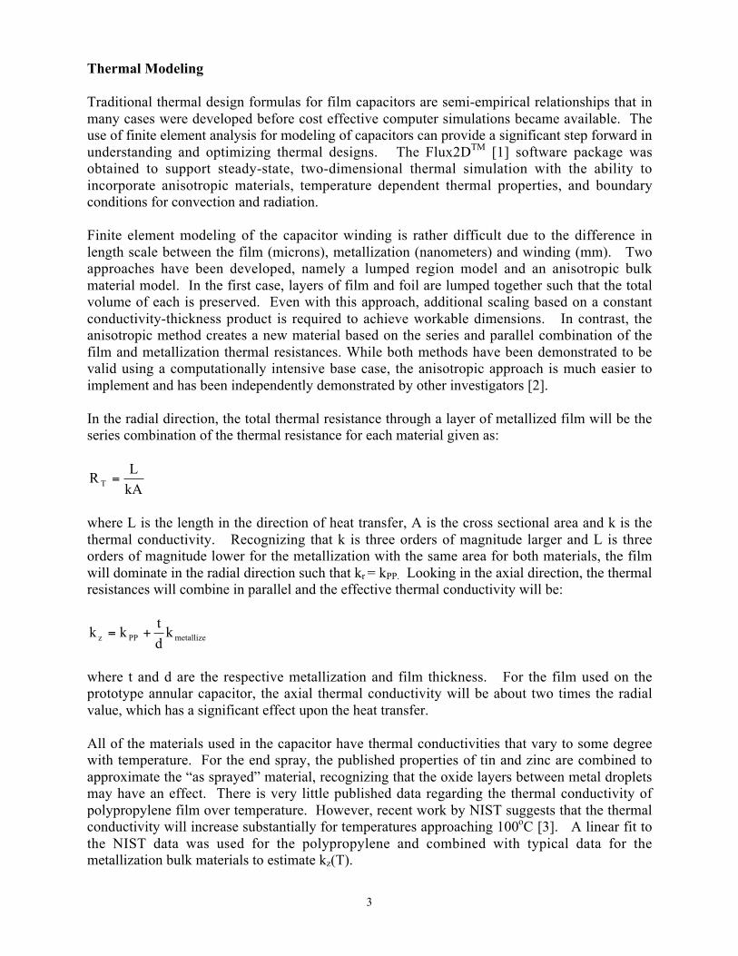
The 1800 µF annular capacitor utilizes 6-micron polypropylene film metallized with a zinc alloyto obtain a worst-case sheet resistance of 6 Ω/square. The 62.5 mm wide film is wound on apolystyrene hollow core having a respective inner and outer diameter of 75 mm and 85 mm. Apolyester tape wrap is applied after winding and the nominal outer diameter of the capacitor is304.8 mm (12 inches). End connections are made by end spray with an initial layer of zincfollowed by an additional layer of tin/zinc alloy. Various contact arrangements are connected tothe end spray using a suitable silver epoxy. A typical capacitor mounted in the ripple current testfixture is shown in Figure 1.
Figure 1. A typical 1800 µF annular capacitor mounted in ripple current test fixture.
An optimistic equivalent series inductance (ESL) for the capacitor can be estimated assuming around conductor on the capacitor axis connecting the electrodes to form a discharge path. For a1” diameter conductor, the ESL will be approximately 26.5 nH. While this number is valid forthe capacitor, the total ESL in a practical circuit will ultimately be defined by the connectiongeometry, which cannot be specified by the capacitor vendor. The equivalent series resistance(ESR) can be readily estimated assuming that losses in the metallized electrodes will dominateover dissipation in the dielectric. For this case, the capacitor internal ESR will be less than 50µΩ , but the resistance of the end spray may be significant depending upon the contactarrangement at the system level.
2
Thermal Modeling
Traditional thermal design formulas for film capacitors are semi-empirical relationships that inmany cases were developed before cost effective computer simulations became available. Theuse of finite element analysis for modeling of capacitors can provide a significant step forward inunderstanding and optimizing thermal designs. The Flux2DTM [1] software package wasobtained to support steady-state, two-dimensional thermal simulation with the ability toincorporate anisotropic materials, temperature dependent thermal properties, and boundaryconditions for convection and radiation.
Finite element modeling of the capacitor winding is rather difficult due to the difference inlength scale between the film (microns), metallization (nanometers) and winding (mm). Twoapproaches have been developed, namely a lumped region model and an anisotropic bulkmaterial model. In the first case, layers of film and foil are lumped together such that the totalvolume of each is preserved. Even with this approach, additional scaling based on a constantconductivity-thickness product is required to achieve workable dimensions. In contrast, theanisotropic method creates a new material based on the series and parallel combination of thefilm and metallization thermal resistances. While both methods have been demonstrated to bevalid using a computationally intensive base case, the anisotropic approach is much easier toimplement and has been independently demonstrated by other investigators [2].
In the radial direction, the total thermal resistance through a layer of metallized film will be theseries combination of the thermal resistance for each material given as:
kA
LRT =
where L is the length in the direction of heat transfer, A is the cross sectional area and k is thethermal conductivity. Recognizing that k is three orders of magnitude larger and L is threeorders of magnitude lower for the metallization with the same area for both materials, the filmwill dominate in the radial direction such that kr = kPP. Looking in the axial direction, the thermalresistances will combine in parallel and the effective thermal conductivity will be:
metallizePPz kd
tkk +=
where t and d are the respective metallization and film thickness. For the film used on theprototype annular capacitor, the axial thermal conductivity will be about two times the radialvalue, which has a significant effect upon the heat transfer.
All of the materials used in the capacitor have thermal conductivities that vary to some degreewith temperature. For the end spray, the published properties of tin and zinc are combined toapproximate the “as sprayed” material, recognizing that the oxide layers between metal dropletsmay have an effect. There is very little published data regarding the thermal conductivity ofpolypropylene film over temperature. However, recent work by NIST suggests that the thermalconductivity will increase substantially for temperatures approaching 100oC [3]. A linear fit tothe NIST data was used for the polypropylene and combined with typical data for themetallization bulk materials to estimate kz(T).
3
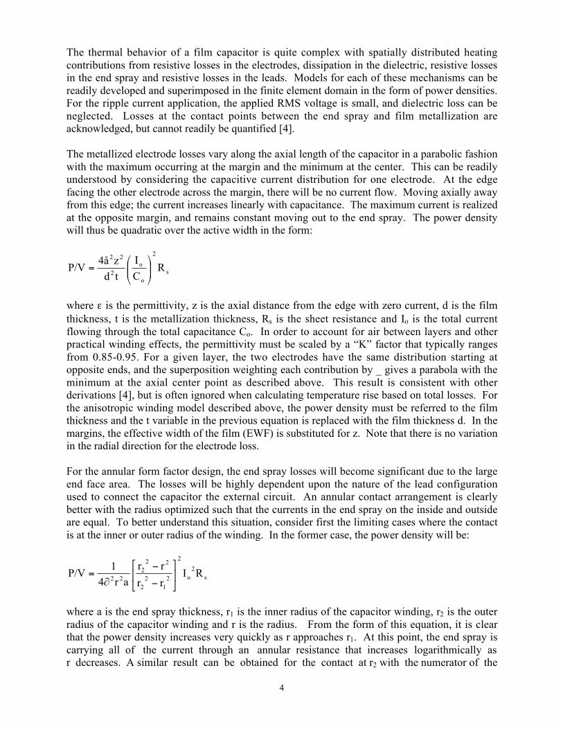
The thermal behavior of a film capacitor is quite complex with spatially distributed heatingcontributions from resistive losses in the electrodes, dissipation in the dielectric, resistive lossesin the end spray and resistive losses in the leads. Models for each of these mechanisms can bereadily developed and superimposed in the finite element domain in the form of power densities.For the ripple current application, the applied RMS voltage is small, and dielectric loss can beneglected. Losses at the contact points between the end spray and film metallization areacknowledged, but cannot readily be quantified [4].
The metallized electrode losses vary along the axial length of the capacitor in a parabolic fashionwith the maximum occurring at the margin and the minimum at the center. This can be readilyunderstood by considering the capacitive current distribution for one electrode. At the edgefacing the other electrode across the margin, there will be no current flow. Moving axially awayfrom this edge; the current increases linearly with capacitance. The maximum current is realizedat the opposite margin, and remains constant moving out to the end spray. The power densitywill thus be quadratic over the active width in the form:
s
2
o
o2
22
RC
I
td
z4åP/V
=
where ε is the permittivity, z is the axial distance from the edge with zero current, d is the filmthickness, t is the metallization thickness, Rs is the sheet resistance and Io is the total currentflowing through the total capacitance Co. In order to account for air between layers and otherpractical winding effects, the permittivity must be scaled by a “K” factor that typically rangesfrom 0.85-0.95. For a given layer, the two electrodes have the same distribution starting atopposite ends, and the superposition weighting each contribution by _ gives a parabola with theminimum at the axial center point as described above. This result is consistent with otherderivations [4], but is often ignored when calculating temperature rise based on total losses. Forthe anisotropic winding model described above, the power density must be referred to the filmthickness and the t variable in the previous equation is replaced with the film thickness d. In themargins, the effective width of the film (EWF) is substituted for z. Note that there is no variationin the radial direction for the electrode loss.
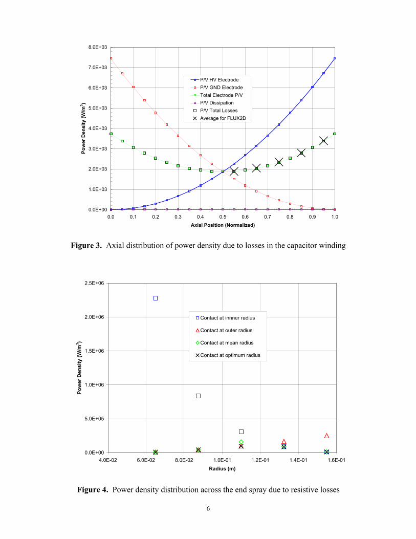
For the annular form factor design, the end spray losses will become significant due to the largeend face area. The losses will be highly dependent upon the nature of the lead configurationused to connect the capacitor the external circuit. An annular contact arrangement is clearlybetter with the radius optimized such that the currents in the end spray on the inside and outsideare equal. To better understand this situation, consider first the limiting cases where the contactis at the inner or outer radius of the winding. In the former case, the power density will be:
s2o
2
21
22
222
22RI
rr
rr
ar4∂
1P/V
−
−=
where a is the end spray thickness, r1 is the inner radius of the capacitor winding, r2 is the outerradius of the capacitor winding and r is the radius. From the form of this equation, it is clearthat the power density increases very quickly as r approaches r1. At this point, the end spray iscarrying all of the current through an annular resistance that increases logarithmically asr decreases. A similar result can be obtained for the contact at r2 with the numerator of the
4

ACTIVE1
ACTIVE2
ACTIVE3
ACTIVE4
ACTIVE5
MARGIN
ENDSPRAY1
ENDSPRAY2
ENDSPRAY3
ENDSPRAY4
Hollow Core
CONTACT
RTV ENDSPRAY5
Center Line
bracketed term modified to be r2-r12. With the contact located at r1 < rc < r2, the limiting case
results can be utilized for the inner and outer annular sections with rc replacing r1 or r2 in thenumerator of the bracketed term. The lowest losses will be realized for the case where rc is suchthat the capacitances on both sides of the contact are balanced.
The axisymmetric finite element domain used for initial analysis of the ring capacitor ispresented in Figure 2.
Figure 2. Illustration of finite element domain for thermal analysis
Half symmetry is assumed about the z-axis and the mid-plane of the capacitor. In order toaccount for spatially distributed losses, the end spray and active volume are segmented intosections that can be assigned individual power densities. The end spray region is composed offive sections of equal annular thickness that have different volumes. The half of the activevolume in the domain is divided into five sections of equal volume. The source region powerdensities for the active volume and end spray regions are presented respectively for a 500 Acurrent at 100 kHz in Figure 3 and Figure 4. Note that the dielectric dissipation is negligiblesince a very low voltage is applied to drive the current at this frequency. The importance ofcontact radius is illustrated through the comparison of various cases for the end spray powerdensity.
Axial Symmetry Line(Mid-Plane)
5
0.0E+00
1.0E+03
2.0E+03
3.0E+03
4.0E+03
5.0E+03
6.0E+03
7.0E+03
8.0E+03
0.0 0.1 0.2 0.3 0.4 0.5 0.6 0.7 0.8 0.9 1.0
Axial Position (Normalized)
Po
wer
Den
sity
(W
/m3 )
P/V HV Electrode
P/V GND Electrode
Total Electrode P/V
P/V Dissipation
P/V Total Losses
Average for FLUX2D
0.0E+00
5.0E+05
1.0E+06
1.5E+06
2.0E+06
2.5E+06
4.0E-02 6.0E-02 8.0E-02 1.0E-01 1.2E-01 1.4E-01 1.6E-01
Radius (m)
Po
wer
Den
sity
(W
/m3 )
Contact at innner radius
Contact at outer radius
Contact at mean radius
Contact at optimum radius
Figure 3. Axial distribution of power density due to losses in the capacitor winding
Figure 4. Power density distribution across the end spray due to resistive losses
6

Color Shade ResultsQuantity : Temperature degrees C.Scale / Color25 / 25.342925.3429 / 25.685825.6858 / 26.028726.0287 / 26.371626.3716 / 26.714526.7145 / 27.057427.0574 / 27.400327.4003 / 27.743227.7432 / 28.086128.0861 / 28.428128.4281 / 28.771928.7719 / 29.114829.1148 / 29.457729.4577 / 29.800629.8006 / 30.143530.1435 / 30.4864
30.5oC
25oC
The end face and outer surface of the capacitor were treated as exchange boundaries having anemissivity of 0.5 and a convection heat transfer coefficient of 5, which is reasonable for free(natural) convection [5]. A Dirichlet boundary was applied across the end face of the contactand all other domain boundaries were set to a Neumann condition such that isotherms must benormal to the surface. With the contact and ambient temperature for the exchange boundary setto 25oC, the temperature profile for the 500 A case at 100 kHz is presented in Figure 5 with thecontact at the optimal location. The total losses are on the order 7 W, but the capacitor aspectratio allows excellent heat transfer such that the total rise at the hot spot is only 5.5 degrees.
Figure 5. Thermal profile for 500 A case at 100 kHz with optimal contact position.
Test Arrangement
A resonant test setup was assembled to support ripple current testing of large value annularcapacitors at 100 kHz as illustrated in Figure 6.
Figure 6. Photograph of the ripple current test stand
7

The sinusoidal waveform was provided by a function generator driving the input of an ENI1500W RF power amplifier. The amplifier output was connected across a coil that wasinductively coupled through free space to a 0.9 µH inductor. A capacitor bank of 2.8 µF inseries with the 1800 µF test capacitor was connected across the inductor terminals. The smallcapacitance dominates the resonance such that the frequency was 100 kHz. The turns ratio andcoupling coefficient were adjusted to match the amplifier output impedance of 50 Ω. Thecapacitor was mounted vertically above the inductor box and exposed only to free convectioncombined with air currents due to ventilation in the building. Temperature measurements wereobtained using J-type thermocouples selected with a rotary switch for readout on an Omega 199controller. Surface measurements were made along the end face in the radial direction withadhesive probes. Measurements at the mid-plane were obtained by inserting probes into smallholes drilled from the end face and distributed in the radial direction. Note that the capacitorswere electrically cleared via applied voltage after drilling the holes.
Comparison of Theoretical and Experimental Results
Initial testing was conducted using a prototype ring capacitor that was already available withcontacts located on only one location on the outside of the ring. While clearly not an optimalconfiguration, this sample was useful to take some initial data and verify the test stand design.Significant heating was observed in the end spray due to the asymmetrical current flow throughthe long path to the bus as expected. Additional prototypes were fabricated with a symmetriccontact arrangement as shown in Figure 1 and Figure 6. An illustration comparing thesymmetric and asymmetric current distributions for the different contact cases is provided inFigure 7.
Figure 7. Illustration of end spray current distribution for symmetric and asymmetric contactschemes
The symmetric contact was comprised of a copper ring soldered to a standard 4” pipe and thenbonded to the capacitor end face with silver epoxy. The contact radius for this case is notoptimal, but was viewed as useful to obtain preliminary data for a symmetrical geometry tocompare with the finite element results. The pipe section was one inch long and terminated witha flat copper plate soldered to the end and bolted to a section of copper flashing runningvertically from the bus. An identical arrangement was used on both sides of the capacitor.
8

0
10
20
30
40
50
60
70
0 20 40 60 80 100 120
Radial Distance from Contact (mm)
Tem
per
atu
re (
oC
)
100 A Calculated (Mid-Plane)
100 A Measured (Mid-Plane)
150 A Calculated (Mid-Plane)
150 A Measured (Mid-Plane)
100 A Calculated (End Face)
100 A Measured (End Face)
150 A Calculated (End Face)
150 A Measured (End Face)
With the symmetrical arrangement, bus heating was found to dominate the thermal profile withthe contact radius being smaller than the optimal case. The measured and calculated steady statetemperature profiles on the capacitor mid-plane and end face are compared in Figure 8 forcurrents of 100 A and 150 A at 100 kHz. The measured surface temperature half way along theaxis of the pipe contact was used to provide a reference temperature for the finite element model.In order to improve the fit, the heat transfer coefficient for the convection boundary conditionswas reduced from 5 to 2, which is still reasonable for free convection. A first order calculationbased on the Grashov number for a vertical flat plate of length scale comparable to the capacitorpredicts a heat transfer coefficient in the range of 1.7 to 2.2 based on accepted empirical data [5].Neglecting internal heating in the capacitor simulation changes the temperature profile by lessthan one degree. Thus, it is clear that the capacitor is simply acting to cool the bus structure andis not the limiting factor for determining how much ripple current can be sustained in the testsetup.
Figure 8. Comparison of calculated and measured temperature profiles for 100 kHz ripplecurrent with an 1800 µF capacitor having a symmetrical contact
9
Conclusions
The annular form factor dry film capacitor offers an excellent solution for switching powersupplies with energy storage and high frequency bypass functionality combined into a singlepackage. Experimental results indicate that bus heating dominates the capacitor hot spottemperature for currents up to 150 A at 100 kHz. Excellent correlation between the experimentaland theoretical results has been demonstrated and the finite element model suggests that currentsexceeding 500 A can be readily handled with proper thermal design of the bus structure.
The symmetrical contact scheme presented here was selected specifically for the purpose ofcomparing the model and experimental data and is not intended to represent an optimalconfiguration for a real application. Having established a solid correlation, various terminaloptions can now be evaluated to take advantage of the extremely low ESR for the annularcapacitor. The end user must recognize that the capacitor thermal performance may ultimatelybe limited by the contact configuration and bus structure rather than internal losses. Future workwill address measurement and modeling for currents exceeding 300 A with consideration ofcurrent rating as a function of the number and location of terminals subject to mechanicalrestrictions in practical systems.
References
[1] Flux2DTM distributed by Magsoft Corporation, 20 Prospect Street, Ballston Spa, New York12020.
[2] M. H. El-Husseini et al, “Thermal Simulation for Geometric Optimization of MetallizedPolypropylene Film Capacitors”, IEEE Trans. Industry Applications, Vol. 38, No. 3, May/June2002, pp 713-718.
[3] T. Kashiwagi et al, “Thermal and Flammability Properties of Polypropylene/CarbonNanotube Nanocomposites”, Polymer 45 (2004) 4227-4239, Elsevier.
[4] S. Boggs et al, “Analysis of the Effects of End Connection Quality on the Dielectric Loss ofMetallized Film Capacitors”, IEEE Trans. Dielectrics and Electrical Insulation, Vol. 11, No. 6,December 2004, pp 990-994.
[5] F. P Incropera and D. DeWitt, Introduction to Heat Transfer 2nd Edition, Wiley, 1990.
10

NOTES
______________________________________________________________________________
______________________________________________________________________________
______________________________________________________________________________
______________________________________________________________________________
______________________________________________________________________________
______________________________________________________________________________
______________________________________________________________________________
______________________________________________________________________________
______________________________________________________________________________
______________________________________________________________________________
______________________________________________________________________________
______________________________________________________________________________
______________________________________________________________________________
______________________________________________________________________________
______________________________________________________________________________
11
SBE, Inc. • 131 South Main Street Tel: 802-476-4146 Web: www.SBElectronics.comBarre, Vermont 05641-4854 USA Fax: 802-476-4149 E-mail: [email protected]
Who we are:
For over 45 years world-class quality film capacitors have been designed and manufactured at ourfacility in Barre, Vermont. The ubiquitous Orange Drop has been the cornerstone of technology forSBE, having served the electronics industry since 1959. Formerly a Sprague Electric company, SBEhas built on that rich history with a renewed focus on providing application specific capacitorsolutions.
Technology and Innovation:
SBE has developed innovative and unique technologies to address demanding requirements in thefields of pulse power, high voltage and high power density. Several patents have already been filed inthese areas to support the growing challenges that designers of power electronics face today. SBE hasworked with companies such as TASER, DRS Optronics, Northrop Grumman and Los Alamos toprovide technology solutions where conventional products fail.
The Power Ring:
SBE’s technology roadmap continually pushes us to think “outside the box”. As part of our E2P2 –Extreme Energy/Pulse Power technology division, we have launched the distinctive Power Ringdry film capacitor series that is specifically tailored to each application. No longer are systemdesigners forced to work around fixed dimensions. The Power Ring now offers the designer flexibilitylike never before.
Experience and Teamwork:
The SBE team is focused on building on the critical success factors that keep us competitive today.Proactive desire to cross-train, weekly production “point team” meetings that track all aspects of WIP,entire plant floor accountability for on-time delivery, set-up reduction programs to reduce leadtimes,and the sharing of productivity metrics and how they affect cost. This culture, combined with ourdesire to lead with technology, provides the core make-up of SBE.