Anomalous Behavior Of SSPC In Highly Crystallized Undoped Microcrystalline Si Films

IEEE TRANSACTIONS ON ELECTRON DEVICES, VOL. 49, NO. 8, AUGUST 2002 1399
An Empirical Model to Determine the Grain Size ofMetal-Induced Lateral Crystallized Film
Victor W. C. Chan and Philip C. H. Chan, Senior Member, IEEE
Abstract—Thin-film transistors (TFTs) have been fabricatedusing the nickel-seeded metal-induced lateral crystallization(MILC), in which an amorphous silicon is crystallized to forma large grain polysilicon film. Single crystal SOI, solid phasecrystallization (SPC), and MILC TFTs were fabricated andthe carrier mobilities extracted. Different types of devices havedifferent variations in electrical properties. An empirical modelbased on the presence of the grain boundaries is proposed toexplain the experimental results. The experimental data was usedto extract the model parameters and the number of grains andgrain size present in the device channel. The results can be furtherused to optimize the crystallization process and the device design.
Index Terms—Grain boundary effect, metal-induced lateralcrystallization (MILC), mobility, modeling, silicon-on-insulator(SOI), surface roughness, thin-film transistor (TFT).
I. INTRODUCTION
POLYSILICON (poly-Si) thin film transistors (TFTs) areattractive in many applications, such as LCD drivers
and the three-dimensional (3-D) integration [1]. However, thelow-temperature poly-Si TFTs have undesirable device charac-teristics. The large variation in device electrical characteristicsis mainly caused by the grain structure, defects, and hencepotential barriers within the grain boundaries. High thresholdvoltage, low mobilities, poor subthreshold slope and highleakage current may result. So, many researches have beenconducted to enhance the grain sizes. One of the promisingtechniques uses metal, such as nickel, to induce the crystal-lization process [2]. Crystallization regions of several tens of
m can be achieved. TFTs fabricated on the metal-inducedlateral crystallization (MILC) film have been reported andthey have superior characteristics compared to the solid phasecrystallization (SPC) poly-Si TFTs [3]–[5]. SPC TFTs aresimilar to MILC TFTs, except that no Ni seeding is applied andhence, no MILC occurs.
Ideally, devices from the crystallized MILC film shouldhave same electrical characteristics as the single crystal sil-icon-on-insulator (SOI) devices. From the experimental result,the MILC devices have large variation, which is caused by theunpredictable grain boundaries. They lead to larger leakagecurrent, lower mobility and higher threshold voltage and highersubthreshold factor [6].
Manuscript received January 1, 2002; revised May 6, 2002. This work wassupported by RGC Earmarked Grants HKUST 6025/97E, HKUST 6140/00E,and CMI 99/00.EG05. The review of this paper was arranged by Editor J. Vasi.
The authors are with the Department of Electrical and Electronic Engi-neering, Hong Kong University of Science and Technology, Hong Kong(e-mail: [email protected]).
Publisher Item Identifier 10.1109/TED.2002.801269.
In this paper, the relationship between grain structure andelectrical characteristics variation is established. Transistorswere fabricated on large grain poly-Si film using the MILCprocess. The SPC and SOI devices were also fabricated forcomparison. The degradation of electrical characteristics inthe MILC devices occurs when the transversal grain bound-aries exist perpendicularly to the direction of carrier flow.Two types of grain boundaries were identified in the MILCregions. One type is the elongated type originated from theNi-seeding window and extends to the MILC front. Other smallgrain regions with grain size are comparable to the partiallycrystallized grains. The grain distribution models were pro-posed for the SPC and MILC devices. For simplification, theone-dimensional (1-D) low-field mobility equations were used.The mobilities of the TFTs are strongly dependent on the grainsizes and boundaries. Model parameters, as well as the numberof grains and grain boundaries present in the device channel,were extracted. The empirical results were also compared toour proposed models.
II. DESCRIPTION OF THEMILC PROCESS
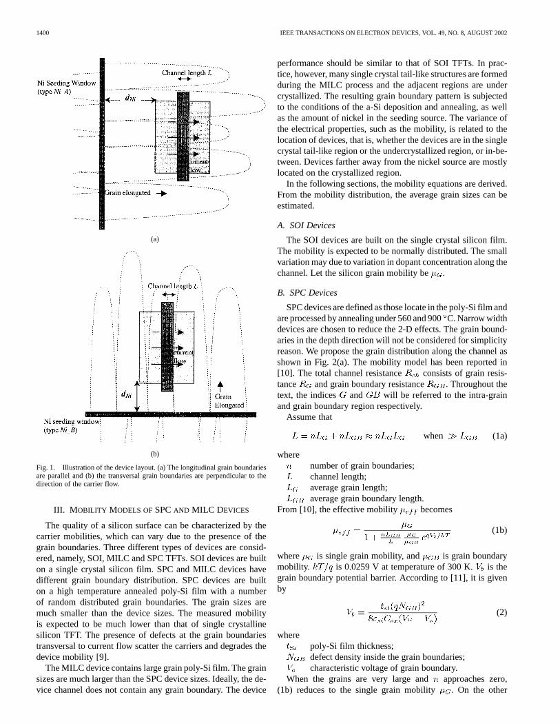
MILC phenomenon has been studied by many researchers[3], [4]. The following explains the occurrence of the singlecrystal tail-like regions. During the MILC at 560C, nickel sili-cide is formed [3], [6], [7]. It has the crystal orientation andcrystal lattice constants close to the crystal silicon. The growthof crystallized silicon begins on any face of the precipitates. Theneedle-like morphology of the crystallization region occurs be-cause the lateral growth of the a-Si/crystallized silicon interfaceoccurs slowly under 560C solid phase crystallization. Mean-while, Ni diffuses faster toward the growing interface and leavesthe epitaxial crystallized silicon. If defect or dislocation occursalong the diffusion paths, nickel will be either blocked or dif-fuse nonuniformly with bending angles. Nickel silicide may ag-glomerate and block the diffusion path. Intermediate regionsmay form between the crystallized and noncrystallized regionsand they can be attributed as grain boundaries. Grain bound-aries may occur and elongate toward the MILC front [8]. Twoadjacent silicon regions may have different orientations and thesmall grains may be difficult to merge. After the second an-nealing at 900 C, the boundaries may still remain.
Fig. 1 illustrates two types of nickel seeding window de-signs and the corresponding transistor regions. Our study fo-cuses on Type Ni_B, which has nickel-seeding strip parallel tothe channel. The grain boundaries are transversal to the directionof the carrier flow. The trapped defect charges become potentialbarriers to the carrier flow.
0018-9383/02$17.00 © 2002 IEEE
1400 IEEE TRANSACTIONS ON ELECTRON DEVICES, VOL. 49, NO. 8, AUGUST 2002
(a)
(b)
Fig. 1. Illustration of the device layout. (a) The longitudinal grain boundariesare parallel and (b) the transversal grain boundaries are perpendicular to thedirection of the carrier flow.
III. M OBILITY MODELS OFSPCAND MILC DEVICES
The quality of a silicon surface can be characterized by thecarrier mobilities, which can vary due to the presence of thegrain boundaries. Three different types of devices are consid-ered, namely, SOI, MILC and SPC TFTs. SOI devices are builton a single crystal silicon film. SPC and MILC devices havedifferent grain boundary distribution. SPC devices are builton a high temperature annealed poly-Si film with a numberof random distributed grain boundaries. The grain sizes aremuch smaller than the device sizes. The measured mobilityis expected to be much lower than that of single crystallinesilicon TFT. The presence of defects at the grain boundariestransversal to current flow scatter the carriers and degrades thedevice mobility [9].
The MILC device contains large grain poly-Si film. The grainsizes are much larger than the SPC device sizes. Ideally, the de-vice channel does not contain any grain boundary. The device
performance should be similar to that of SOI TFTs. In prac-tice, however, many single crystal tail-like structures are formedduring the MILC process and the adjacent regions are undercrystallized. The resulting grain boundary pattern is subjectedto the conditions of the a-Si deposition and annealing, as wellas the amount of nickel in the seeding source. The variance ofthe electrical properties, such as the mobility, is related to thelocation of devices, that is, whether the devices are in the singlecrystal tail-like region or the undercrystallized region, or in-be-tween. Devices farther away from the nickel source are mostlylocated on the crystallized region.
In the following sections, the mobility equations are derived.From the mobility distribution, the average grain sizes can beestimated.
A. SOI Devices
The SOI devices are built on the single crystal silicon film.The mobility is expected to be normally distributed. The smallvariation may due to variation in dopant concentration along thechannel. Let the silicon grain mobility be .
B. SPC Devices
SPC devices are defined as those locate in the poly-Si film andare processed by annealing under 560 and 900C. Narrow widthdevices are chosen to reduce the 2-D effects. The grain bound-aries in the depth direction will not be considered for simplicityreason. We propose the grain distribution along the channel asshown in Fig. 2(a). The mobility model has been reported in[10]. The total channel resistance consists of grain resis-tance and grain boundary resistance . Throughout thetext, the indices and will be referred to the intra-grainand grain boundary region respectively.
Assume that
when (1a)
wherenumber of grain boundaries;channel length;average grain length;average grain boundary length.
From [10], the effective mobility becomes
(1b)
where is single grain mobility, and is grain boundarymobility. is 0.0259 V at temperature of 300 K. is thegrain boundary potential barrier. According to [11], it is givenby
(2)
wherepoly-Si film thickness;defect density inside the grain boundaries;characteristic voltage of grain boundary.
When the grains are very large and approaches zero,(1b) reduces to the single grain mobility . On the other

CHAN AND CHAN: GRAIN SIZE OF MILC FILM 1401
(a)
(b)
Fig. 2. Schematic diagrams show (a) SPC and (b) MILC devices. Assume SPC devices haven grains andn grain boundaries. MILC devices havem singlecrystal tail-like regions andn grains in the undercrystallized region.
hand, if grains are very small and becomes very large,the second term in the denominator of (1b) is dominant and(1b) becomes the classical mobility model for a poly-TFT
[10] where is the intrinsic mobilityof the material.
Equation (1b) is written as
(3a)
where
(3b)
is a characteristic length, which is a constant in the samechannel media. is dependent on the grain sizes andthe characteristic length . If the grain sizes are evenly dis-tributed, is weakly related to the channel length.
The grain size variation has been studied using the Poissondistribution [12]. The probability that exactly grain bound-aries occurred within a device is
(4)
where is the mean value of grain boundaries. Using the em-pirical data of many devices with same size, the mean of themobility is obtained. The average grain size can be ex-tracted from (3a) and (3b). The empirical mobility distributioncan be extracted using the model in (4) and substituted to (3a).
C. MILC Devices
Suppose a device is distributed within the single crystaltail-like region and undercrystallized region. The grain distri-bution is schematically shown in Fig. 2(b). There aresmallgrains and grain boundaries within the undercrystallized area,and tail-like single-crystal big grains and correspondingboundaries, provided . In the following text,bigandsmallare referred to the elongated single crystal grain anduncrystallized grain, respectively.
The channel length is then
(5a)
where is the average grain length and is the averagegrain boundary length. Assume , thechannel length becomes
(5b)
Suppose the total channel resistance consists of total grainresistance and grain boundary resistance . Using thestandard MOSFET theory, can be derived [10]
(6a)
where is the channel width and is the charge in theinversion layer. With the relationship between and

1402 IEEE TRANSACTIONS ON ELECTRON DEVICES, VOL. 49, NO. 8, AUGUST 2002
mentioned in [10], assume that the grain boundarywidths and are small and equal to ,and consider the assumption in (5b) and (6a) can be simplifiedand becomes
(6b)
It can be further simplified to
(7a)
where
(7b)
is another characteristic length, which is a constant in thesame channel media. is dependent on the number of singlecrystal tail-like regions , number of small grains within un-dercrystallized regions, the device channel length and thecharacteristic length . In this case, is strongly dependenton the location of the devices. The grain size has been studiedusing the Poisson distribution [12]. The probabilities that ex-actly and grain boundaries occurred within a device aresimilar to (4). is replaced by and , which are the meanvalues of tail-like structure and grain boundaries within theundercrystallized region, respectively. Suppose and aretwo independent variables, the joint probability density function
is
(8)
In this paper, the mobility of MILC devices with differentchannel length is characterized. The sum of the average numberof large and small grains ( ) can be determinedexperimentally. However, the values of and cannot bedirectly derived. The method of determining and will beprovided in Section IV-C.
IV. EXPERIMENTAL RESULTS AND DISCUSSION
Three different types of PMOSFETs were fabricated, namelySOI, SPC, and MILC TFTs. All the devices have channel thick-ness of 1000 Å and gate oxide of 120 Å. The nickel-seedingwindow is 30 m away from the device channel and is par-allel to the carrier flow [Fig. 1(b)]. The electrical performancehas been reported in [13]. The low field mobility is ex-tracted using the linear region characteristics of the MOSFETswith V. All the transistors have small gate width toreduce the lateral grain boundary effect.
A. SOI Devices
A large number of devices have been characterized. The ex-tracted mobility is 100 cm/V-s with 8% variation. We assumethat this is the single grain mobility and will be used in thefollowing sections.
B. SPC Devices
Narrow width SPC devices were considered. They hadchannel length of 9.8 m and channel width of 0.48m. The
Fig. 3. Comparison of cumulative distribution of mobility model (solidline) to experimental data (square dots) from PMOS SPC TFTs withL=W = 9:8/0.48�m.
Fig. 4. Cumulative distribution of experimental data from PMOS MILCTFTs with varying channel lengths. The result of SOI TFTs is also includedfor comparison.
low-field mobility of each device were extracted. The means ofmobility is 8 cm /V-s, if the and are fixed at 5.0 and0.05 V, respectively. All devices related data must be computedfirst before the average grain size can be calculated. In theparameter extraction, we chose nm, V and
cm /V-s [10]. Using the technique described in [9],[14], the trap density is estimated to be 1 10 /cm .From (2) and (3b), is calculated to be 0.0329 V and to be3.56 m. Using these values, (3a) becomes
(9a)
where is the average grain size inm. If the average mo-bility is 8 cm /V-s, the derived mean of grain size is 0.31m and

CHAN AND CHAN: GRAIN SIZE OF MILC FILM 1403
TABLE IAVERAGE LOW-FIELD MOBILITIES AND SUM OF GRAIN BOUNDARIES FORPMOS MILC TFTs WITH VARYING CHANNEL LENGTHS
there are 32 grains along the channel on average. The Poissondistribution in (4) becomes
(9b)
where is the number of grain boundaries. If (9a) is substitutedinto (9b), it becomes
(9c)
for devices of m. The cumulative distributions ofthe mobility calculated using the model and experimental dataare compared in Fig. 3. The empirical model can be reasonablyfitted to the experimental data. The model provides quantita-tive understanding of the effect of the grain boundaries on themobility of the MILC devices. However, the 1-D ideal case isconsidered. The real devices have grain boundaries in three di-mension in the channel depth and channel width directions. Thismay explain some of the discrepancies between the model andexperimental data.
C. MILC Devices
Narrow width MILC devices were used for the data extrac-tion. They had channel width of 0.48m. Devices with channellengths from 0.8 to 10 m were measured. The same measure-ment condition used for the SPC devices was applied to extractthe low-field mobilities, except that V. Thereason that we applied lower in this case is because MILCdevices have lower threshold voltage. The cumulative proba-bilities are plotted in Fig. 4. The result of SOI devices is alsoincluded for comparison. From the figure, the variation of theMILC devices becomes smaller when the channel is reducedfrom 10 to 0.8 m. The distribution also approaches to that ofthe SOI devices, which has a narrower distribution and has highmobility.
The parameters considered for the modeling were stated inthe last section. The trap density for these device was5 10 /cm [14]. From (2) and (7b), was calculated to be0.0136 V and be 1.69 m. Equation (7a) becomes
(10)
is in the unit of m. The extracted means of the mobility fordevices with varying channel lengths are tabulated in Table I.Substituting the average mobilities into (10), the summation ofthe two different grains ( ) can be calculated(Table I). For the cases of channel length and 0.8 m,
. This suggests that the tail-like regions have
Fig. 5. Comparison of cumulative distribution of mobility model (solid anddot lines) to experimental data (open symbol) from PMOS MILC TFTs withL = 10 and 5�m, respectively.
width larger than 2 m. No grain boundaries are expected inthe channel of these devices. The above model is not applicableto any short channel devices.
Unfortunately, and cannot be derived separately. From(5b) and Table I, we retain
for to (11a)
and
for to (11b)
From the different combinations of and , andcan be estimated. The average width of the tail-like
region ( ) is 4.1 m and the average grain size in the un-dercrystallized region ( ) is 0.4 m.
The Poisson distribution [from (8)] is reconsidered for thecases and 5 m, provided that , the cu-mulative probabilities are plotted in Fig. 5. The experimentaldata are also included for comparison. The empirical model canreasonably fit to the experimental results.
When the devices have channel lengths less than 4.1m, theabove model is not applicable because the transistors are smalland may be located entirely either on single crystal tail-like re-gions, or in the undercrystallized regions, or between the tworegions. Therefore, the modeling result is not valid.

1404 IEEE TRANSACTIONS ON ELECTRON DEVICES, VOL. 49, NO. 8, AUGUST 2002
The derived data, such as the average width of the tail-likeregions and average grain size in the undercrystallized regions,are accurate if the actual grain distribution follows our purposed1-D model [Fig. 2(b)]. Moreover, the results are only applicableto this particular experiment. They are subjective to the filmquality in the device channel, which is dependent on the processconditions of the a-Si deposition and the MILC process, such asprocess temperature and time. However, the models do providequantitative understanding of the effect of the grain boundarieson the mobility of the MILC devices.
There are some discrepancies between the experimental dataand our model. Our model assumes 1-D ideal case. Practicaldevices are three-dimensional. The grain boundaries should beconsidered in the channel depth as well as in the channel widthdirections. The grain boundary close to the drain also effec-tively affects the mobility, especially when drain potential islarge. This is because the existence of grain boundaries affectsthe maximum electrical field in this region. The summation ofall possible grain boundary effects makes the analysis morecomplicated.
V. CONCLUSION
TFTs fabricated using the MILC technique were reported.Two types of grain boundaries were observed in the MILC re-gions. They are the tail-like crystallization region and the un-dercrystallized region. The effects of grain boundaries on the de-vice mobility were investigated. A mobility model is studied andapplied to estimate the numbers of grain boundaries present inthe device channel. The model is used to quantify the statisticalvariation of electrical characteristics of SPC and MILC devices.Our results show that the average grain size inside the under-crystallized region (solid phase crystallization only) is 0.4mand 4.1 m inside the single crystal tail-like region, whereas theaverage grain size of the SPC TFTs is only 0.31m.
The occurrence of grain boundaries is not predictable and theeffect cannot be eliminated totally. Further optimization of thedesign of the devices is necessary. From the derived result, theaverage width of the single crystal tail-like structure is 4.1m.Devices with channel length and width less than 4m can re-duce the occurrence of grain boundaries located within the de-vice channel.
REFERENCES
[1] Z. Meng, M. Wang, and M. Wong, “High performance low temperaturemetal-induced unilaterally crystallized polycrystalline silicon thin filmtransistors for system-on-panel applications,”IEEE Trans. Electron De-vices, vol. 47, pp. 404–409, Feb. 2000.
[2] H. Wang, M. Jagar, V. M. C. Poon, M. Qin, Y. Wang, and P. K. Ko,“Super thin film transistor with SOI CMOS performance formed by anovel grain enhancement method,”IEEE Trans. Electron Devices, vol.47, pp. 1580–1586, Aug. 2000.
[3] C. Hayzelden and J. K. Batstone, “Silicide formation and silicide-medi-ated crystallization of nickel-implanted a-Si thin films,”J. Appl. Phys.,vol. 73, no. 12, pp. 8279–8289, June 1993.
[4] C. Hayzelden, J. K. Batstone, and R. C. Cammarata, “In situ transmis-sion electron microscopy studies of silicide-mediated crystallization ofa-Si,” Appl. Phys. Lett., vol. 60, pp. 225–227, Jan. 1992.
[5] M. Yoshimura, I. Ono, and K. Ueda, “STM observation of nickel sili-cides on Si (001),”Appl. Phys. A, vol. 66, no. 7, pp. S1043–S1045, 1998.
[6] K. N. Tu, J. W. Mayer, and L. C. Feldman,Electronic Thin Film Sci-ence: For Electrical Engineers and Materials Scientists. New York:Macmillan, 1992, ch. 10, 12, 15.
[7] K. Graff, Metal Impurities in Silicon Device Fabrication, 2nded. Berlin, Germany: Springer-Verlag, 2000, ch. 4.
[8] D. Murley, N. Young, M. Trainer, and D. McCulloch, “An investiga-tion of laser annealed and metal induced crystallized polycrystalline sil-icon thin film transistors,”IEEE Trans. Electron Devices, vol. 48, pp.1145–1151, June 2001.
[9] J. H. Schon and B. Batlogg, “Trapping in organic field-effect transis-tors,” J. Appl. Phys., vol. 89, pp. 336–342, Jan. 2001.
[10] F. V. Farmakis, J. Brini, G. Kamarinos, C. T. Angelis, C. A. Dimitriadias,and M. Miyasaka, “On current modeling of large grain polycrystallinesilicon thin film transistor,”IEEE Trans. Electron Devices, vol. 48, pp.701–706, Apr. 2001.
[11] H. K. Chen and C. Y. Wu, “An analytical grain barrier height modeland its characterization for intrinsic poly-Si thin film transistors,”IEEETrans. Electron Devices, vol. 45, pp. 2245–2247, Oct. 1998.
[12] A. W. Wang and K. C. Saraswat, “A strategy for modeling of variationsdue to grain size in polycrystalline thin-film transistors,”IEEE Trans.Electron Devices, vol. 47, pp. 1035–1043, May 2000.
[13] V. W. C. Chan and P. C. H. Chan, “High performance gate-all-arounddevices using metal induced lateral crystallization,” inIEEE SOI Conf.,Oct. 2000, pp. 112–113.
[14] J. Y. W. Seto, “The electrical properties of polycrystalline silicon films,”J. Appl. Phys., vol. 46, pp. 5247–5253, Dec. 1995.
Victor W. C. Chan received the B.E. degree in elec-trical engineering from the University of New SouthWales, Sydney, Australia, in 1995. He is currentlypursuing the Ph.D. degree in the Department of Elec-trical and Electronic Engineering, Hong Kong Uni-versity of Science and Technology, Hong Kong.
From 1996 to 1998, he was an Etch Process Engi-neer with Chartered Semiconductor Manufacturing,Ltd., Fab3 Pilot, Singapore. His research interestsinclude fabrication and analysis on CMOS SOI andnovel devices, such as double-gate structure, 3-D
integrated circuits and stacked SRAM cells, polysilicon crystallization, ande-beam mix-and-match techniques.
Philip C. H. Chan (SM’95) was born in Shanghai,China, and raised in Hong Kong. He receivedthe B.S. degree in electrical engineering from theUniversity of California, Davis, where he graduatedwith highest honors and departmental citation. Hereceived the M.S. and Ph.D. degrees in electricalengineering from the University of Illinois, Urbana,under Professor C. T. Sah.
He was with the University of Illinois as an IBMPostdoctoral Fellow and later as Visiting AssistantProfessor in electrical engineering. While there,
he engaged in semiconductor device and material research. He also taughtundergraduate and postgraduate courses in semiconductor devices. He joinedIntel Corporation, Santa Clara, CA, in 1981 as a Senior Engineer in theTechnology Development Computer-Aided Design Department. Later, hebecame a Principal Engineer and Senior Project Manager. He has the corporateresponsibility for circuit simulation tools, VLSI device modeling, and processcharacterization. In 1990, he transferred to the Design Technology Departmentof Microproducts Group. There he led a team of engineers that defined anddeveloped a CAD system to design multichip module products. This effort ledto the first functional 486-based multichip module at Intel. He joined the HongKong University of Science of Technology (HKUST) in April 1991 as a Reader.He became a Professor in 1997. He served as the Director of UndergraduateStudies, the founding Director of Computer Engineering Programme, theAssociate Dean of Engineering, and the Acting Head and then Head of theDepartment of Electrical and Electronic Engineering. He is also Director ofMicroelectronics Fabrication Facility at HKUST. His research interests includemicroelectronics devices, circuits, integrated sensors, and electronic packaging.