An Automatic Design Flow for Implementation of Side...
10
N. Azemard and L. Svensson (Eds.): PATMOS 2007, LNCS 4644, pp. 330–339, 2007. © Springer-Verlag Berlin Heidelberg 2007 An Automatic Design Flow for Implementation of Side Channel Attacks Resistant Crypto-Chips Behnam Ghavami and Hossein Pedram Computer Engineering Department, Amirkabir University of Technology (Tehran Polytechnic),424 Hafez Ave, Tehran 15785, Iran {ghavami,pedram}@ce.aut.ac.ir Abstract. Recently, it has been proven that asynchronous circuits possess con- siderable inherent countermeasure against side channel attacks. In spite of these systems' advantages for immune cryptography, because of the lack of automatic design tools and standard methods, exploiting such schemes faces difficulties. In this paper, a fully automated secure design flow and a set of secure library cells resistant to power analysis and fault injection attacks are introduced for QDI asynchronous circuits. In this flow a standard cell library has been intro- duced which has resistance to differential power analysis on faulty hardware at- tack. The results show that using this scheme is approximately 5.62 times more balanced than the best cells designed using previous synchronous balancing methods. To verify the efficiency of our presented flow we applied it to imple- mentation of the AES cryptography algorithm. Also, this implementation shows a 2.8 times throughput improvement over the synchronous implementation us- ing the same technology. 1 Introduction Cryptography algorithms have an important part of today’s digital society to ensure the confidentiality of sensitive information. To obtain security, contemporary strong cryptography algorithms are designed to withstand rigorous cryptanalysis. The degree of complexity of the algorithm which implies the resistibility of the algorithm ex- posed to the attacks is discussed in the realm of cryptanalysis. The validity of mathe- matical security models for the algorithms is based on the fact that the attackers don’t have access to the intermediate computational data. So any kind of information about these intermediate data will simplify the crypto analysis dramatically. Since cryptog- raphy algorithms in mathematics perspective have high security, nowadays attackers turn to analyzing the physical aspects of system to achieve the intermediate computa- tional data. Leaked information from physical side channels and information resulted from mathematical model of algorithm, are used in these kinds of attacks. There are some kinds of attacks which take advantage of the implemented physical properties and leaked information from side channels [1][2][3][4]. These attacks which exploit the physical specific weaknesses are known as side channel attacks. Several solutions have been proposed to countermeasure against side channel attacks both in software and hardware level [4][5][6][7]. Recently, in addition to
Transcript of An Automatic Design Flow for Implementation of Side...
N. Azemard and L. Svensson (Eds.): PATMOS 2007, LNCS 4644, pp. 330–339, 2007. © Springer-Verlag Berlin Heidelberg 2007
An Automatic Design Flow for Implementation of Side Channel Attacks Resistant Crypto-Chips
Behnam Ghavami and Hossein Pedram
Computer Engineering Department, Amirkabir University of Technology (Tehran Polytechnic),424 Hafez Ave, Tehran 15785, Iran
{ghavami,pedram}@ce.aut.ac.ir
Abstract. Recently, it has been proven that asynchronous circuits possess con-siderable inherent countermeasure against side channel attacks. In spite of these systems' advantages for immune cryptography, because of the lack of automatic design tools and standard methods, exploiting such schemes faces difficulties. In this paper, a fully automated secure design flow and a set of secure library cells resistant to power analysis and fault injection attacks are introduced for QDI asynchronous circuits. In this flow a standard cell library has been intro-duced which has resistance to differential power analysis on faulty hardware at-tack. The results show that using this scheme is approximately 5.62 times more balanced than the best cells designed using previous synchronous balancing methods. To verify the efficiency of our presented flow we applied it to imple-mentation of the AES cryptography algorithm. Also, this implementation shows a 2.8 times throughput improvement over the synchronous implementation us-ing the same technology.
1 Introduction
Cryptography algorithms have an important part of today’s digital society to ensure the confidentiality of sensitive information. To obtain security, contemporary strong cryptography algorithms are designed to withstand rigorous cryptanalysis. The degree of complexity of the algorithm which implies the resistibility of the algorithm ex-posed to the attacks is discussed in the realm of cryptanalysis. The validity of mathe-matical security models for the algorithms is based on the fact that the attackers don’t have access to the intermediate computational data. So any kind of information about these intermediate data will simplify the crypto analysis dramatically. Since cryptog-raphy algorithms in mathematics perspective have high security, nowadays attackers turn to analyzing the physical aspects of system to achieve the intermediate computa-tional data. Leaked information from physical side channels and information resulted from mathematical model of algorithm, are used in these kinds of attacks. There are some kinds of attacks which take advantage of the implemented physical properties and leaked information from side channels [1][2][3][4]. These attacks which exploit the physical specific weaknesses are known as side channel attacks.
Several solutions have been proposed to countermeasure against side channel attacks both in software and hardware level [4][5][6][7]. Recently, in addition to
An Automatic Design Flow for Implementation of Side Channel 331
asynchronous circuit design advancements [18], it became clear that this design methodology is suitable for the secure cryptography systems. Since the clock signal has been eliminated in asynchronous circuits, these are resistant to the fault injection in clock. Clock elimination attenuates electromagnetic radiation leading to much increased complexity in these types of attacks. Power consumption in the dual rail QDI asynchronous circuits is independent of input data [11], so these circuits are countermeasure to differential power attacks.
The purpose of this paper is to present a new method to eliminate the physical limi-tations of contemporary cryptography systems. This methodology prepares a complete design cycle of secure cryptography systems by introducing a practical commercial quality Electronic design Automation (EDA) synthesis tool, which elimi-nates all sources of leaked information from side channels. The design flow presented here is based on a QDI asynchronous circuits in which customized standard cells have been used. This method not only preserves performance but also is a suitable solution for promoting countermeasure against power, timing and fault injection attacks at the same time. Also, circuits implemented by this method have been resistant to the new and effective attack which is made up of fault injection and power analysis.
2 Motivation
Countermeasures against side-channel analysis are necessary to pass certification of semiconductor products for security applications like smart cards. To prevent side-channel attacks, several countermeasures solution has been proposed which aim to reduce or eliminate the amount of information which can be inferred about intermedi-ate data in a hardware implementation of a cryptographic algorithm [4][5][6][7][10].
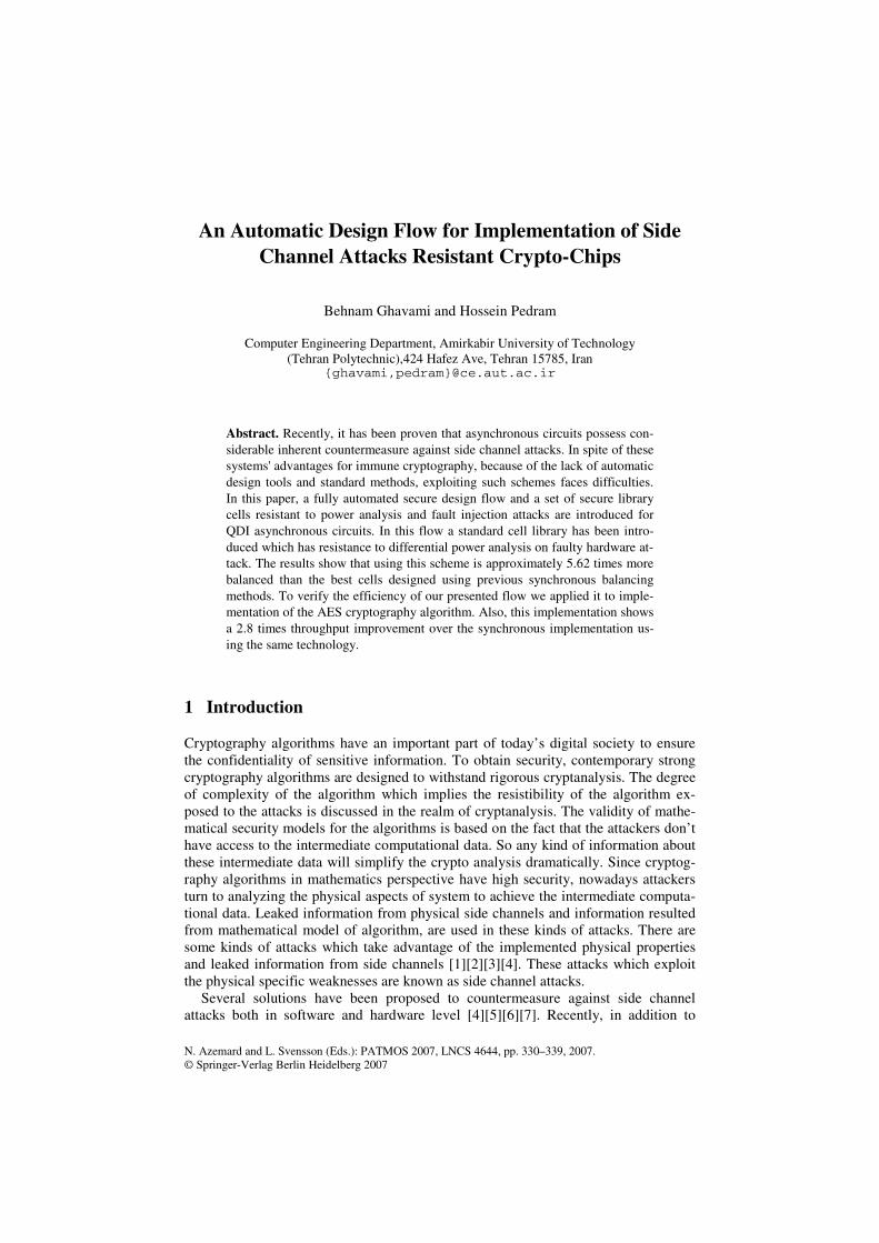
One of the most effective countermeasures against power analysis attacks is based on the use of specially designed balanced gates for which the power consumption is equal for all data and all transitions of the gate. Several such gates have been previ-ously presented (SABL [5], DyCML [6], BSDT [14], WDDL [7]). The SABL [15] gate is based on the strongArm 110 flip-flop. It keeps the sense amplifier half of the flip-flop and replaces the input differential pair by a differential pull down network (Figure 1). WDDL [7] constructed from regular standard cells and is applicable to FPGA. F. Mace and etc. in [6], suggest using the Dynamic Current Mode Logic (DyCML) to counteract power analysis. They investigated use of dynamic and differ-ential logic styles to counteract power analysis attack. In compared the SABL gates with DyCML [6], exhibited that both logic styles allow to significantly decreasing the circuit energy variations if compare them with a standard CMOS technology but sig-nificantly reduces the power delay product.
However, most of this approaches, such as those from [5][6] have no countermea-sures against glitch and fault-injection attacks and require additional protection. More importantly, since differential and dynamic (DD) approaches from [5][6], require dynamic logic cell design. The usage of DD gates is limited to custom or semi-custom design that greatly limits the perceived universality of DD based circuitry. In [7], two major reasons why EDA support of dynamic logic based design is very difficult for synchronous methodology was discussed. According to it each synchronous dynamic gate requires a clock input and uses both levels of clock signal – it means that from
332 B. Ghavami and H. Pedram
(a) (b) (c)
Fig. 1. (a). Balanced NAND gate proposed by Cryptographic Research [15]. (b). SABL XOR gate [5]. (c). DyCML XOR gate[6].
the point of view of EDA tools each gate behaves like a flip-flop. Second, due to early/late arrival, charge sharing, clock distribution problems with small clocking granularity and uncertainty about worst case delay makes static timing analysis (STA) of dynamic circuits very problematic. As these problems make power balanced dy-namic circuitry practically unavailable for rapid ASIC development the researchers resort to less secure (e.g. less balanced) but easier to implement solutions based on standard static non-balanced gate libraries.
A design methodology based on dynamic asynchronous micropipelines which eliminate the lake of secure hardware design flow (SHDF) was proposed [8]. Their methodology allows incorporation of existing synchronous dynamic gate designs and circuit structures. The combination of asynchronous operation and balanced dynamic gates allows automated design highly resistant to side-channel attacks. Also, a bal-anced library was specifically designed for the fine-grained asynchronous template (Balanced Symmetric with Discharge Tree (BSDT) gates [14]).
All the currently known balanced gate designs require considerable hardware re-dundancy and overhead to ensure balanced computations [14][6][7]. Much of this redundant hardware is not directly associated with the logical or Boolean function of the gate; it is present to ensure power balance during computations. Weaknesses in the present balanced gate designs exist due to the redundancy of the gate; there exist many internal transistor level faults which will not affect the Boolean function of the gate but will affect the balance of the gate. As shown in [9], a small number of faults can potentially make power analysis attacks feasible even on protected devices. This vulnerability opens the possibility of new and effective methods of attacks, based on a combination of fault and power attack.
Our approach incorporates dynamic gate balancing techniques and methods with asynchronous design principles to address the timing and clock related problems as-sociated with current and future balanced dynamic gate designs and to enable their use in automatic standard-cell based design flow.
3 QDI Asynchronous Circuits
An asynchronous circuit is composed of individual modules which communicate to each other by means of point-to-point communication channels. Therefore, a given

An Automatic Design Flow for Implementation of Side Channel 333
module becomes active when it senses the presence of an incoming data. It then per-forms the computation and sends the result via output channels. Communications through channels are controlled by handshake protocols [18]. An asynchronous circuit is called delay-insensitive (DI) if it preserves its functionality, independent of the delays of gates and wires [18]. Quasi delay-insensitive (QDI) circuits are like DI circuits with a week timing constraint: isochronic forks.
The encodings of the channels can be in a variety of ways. Return to zero hand-shaking protocol with dual-rail data encoding that switch the output from data to spacer and back is the most common QDI implementation form. We use a dual rail encoding. The data channel contains a valid data (token) when exactly one of 2 wires is high. When the two wires are lowered the channel contains no valid data and is called to be neutral (Figure 2). One of the major protocols used in asynchronous cir-cuits is four-phase protocol. In a four-phase protocol's sequence a receive action con-sists of four steps. (1) Wait for input to become valid. (2) Acknowledge the sender after the computation performed Lack. (3) Wait for inputs to become neutral. (4) And lower the acknowledgement signal. A send action consists of four phases: (1) send a valid output. (2) Wait for acknowledge. (3) Make the output neutral. (4) Wait for acknowledge to lower. As it has been mentioned, using four-phase handshaking pro-tocol with dual-rail data encoding caused data independent time and power emissions which necessary for Side channel attacks resistant crypto-chips.
d.t d.f
Neutral(“E”) 0 0 Valid ‘0’ Valid ’1’
0 1
1 0
Not used 1 1
Fig. 2. Dual rail coding
Many of the properties which many designers try to artificially add to synchronous cryptography designs are natural in QDI asynchronous circuits. In these circuits, no clock caused clock glitch attacks are removed. In furthermore, Electromagnetic signa-ture is strongly reduced by replacing a synchronous processor with an asynchronous one (no clock harmonics) [19]. Asynchronous circuits typically use a redundant en-coding scheme (e.g. dual-rail). This mechanism provides a means to encode an alarm signal. Circuits comprising dual-rail (or multi-rail) codes can be balanced to reduce data dependent emissions. In the above illustration whether we have a logical-0 or a logical-1, the encoding of the bit ensures that the data is transmitted and computations are performed with constant Hamming weight. This is important since side-channel analysis is based on the leakage of the Hamming weight of the sensitive data [2]. Whilst dualrail coding might be used in a clocked environment one would have to ensure that combinational circuits were balanced and glitch free. Return to-zero (RTZ) signaling is also required to ensure data independent power emissions.

334 B. Ghavami and H. Pedram
4 Persia: A Synthesis Tool for QDI Circuits
Persia is an asynchronous synthesis toolset developed for automatic synthesis of QDI asynchronous circuits with adequate support for GALS systems. The structure of Persia is based on the design flow shown in Figure 3 which can be considered as the following four individual portions: QDI synthesis, GALS synthesis, layout synthesis, and simulation at various levels. QDI and GALS synthesis flows are join together in the layout stage. The simulation flow is intended to verify the correctness of the syn-thesized circuit in all levels of abstraction. In this paper we only brief QDI synthesis flow for it security benefit.
Persia synthesis approach is based on pre-design asynchronous four-phased dual rail templates. It uses PCFBs [18] for its predefined templates (Figure 4). Persia uses Verilog-CSP [17], an extension of the standard Verilog which supports asynchronous communications as the hardware description language for all levels of abstractions except the netlist which uses standard Verilog. The input of Persia is a Verilog-CSP description of a circuit. This description will be converted to a netlist of standard-cell elements through several steps of QDI synthesis flow. In the following subsections we briefly describe the functionality of these three stages.
Fig. 3. Persia synthesis flow[16] Fig. 4. The 1-bit PCFB buffer
4.1 Arithmetic Function Extractor (AFE)
Technology-Mapper, as a part of Template Synthesizer, is only able to synthesize one-bit assignments containing logical operators like AND, OR, XOR, etc. Arithmetic operations are not synthesizable by Template Synthesizer, so Persia extracts these operations from the CSP source code and then implements them with pre-synthesized standard templates. This is the role of the first stage of our asynchronous synthesis flow, called Arithmetic Function Extractor (AFE). AFE extracts each assignment that contains arithmetic operations like addition, subtraction, comparison, etc and gener-ates a tree of standard circuits which implements the extracted assignment. The

An Automatic Design Flow for Implementation of Side Channel 335
communication between the main circuit and the arithmetic circuit is made by intro-ducing new channels and added read/write [17] macros. As a result, the main circuit will contain only logical assignments and arithmetic computations will be performed in standard unconditional modules that are designed and included in the library.
4.2 Decomposition
The high-level CSP description of even very simple practical circuits is not directly convertible to PCFB [18] templates. The intention of Decomposition stage is to de-compose [20] the original description into an equivalent collection of smaller interact-ing processes that are compatible to these templates and are synthesizable in next stages of QDI synthesis flow. Decomposition also enhances the parallelism between the resultant processes by eliminating unnecessary dependencies and sequences in the original CSP description.
4.3 Template Synthesizer (TSYN)
Template Synthesizer, as the final stage of QDI synthesis flow, receives a CSP source code containing a number of PCFB-compatible modules and optionally a top-level netlist and generates a netlist of standard-cell elements with dual-rail ports that can be used for creating final layout. TSYN can synthesize all logical operations including AND, OR, XOR, etc with conditional or unconditional READ and WRITES. In addi-tion, TSYN adds acknowledge signals to I/O ports and converts the top-level netlist to dual-rail form and makes appropriate connections between ports and acknowledge signals. The output of TSYN can be simulated in standard Verilog simulators by us-ing the behavioral description of standard-cell library elements.
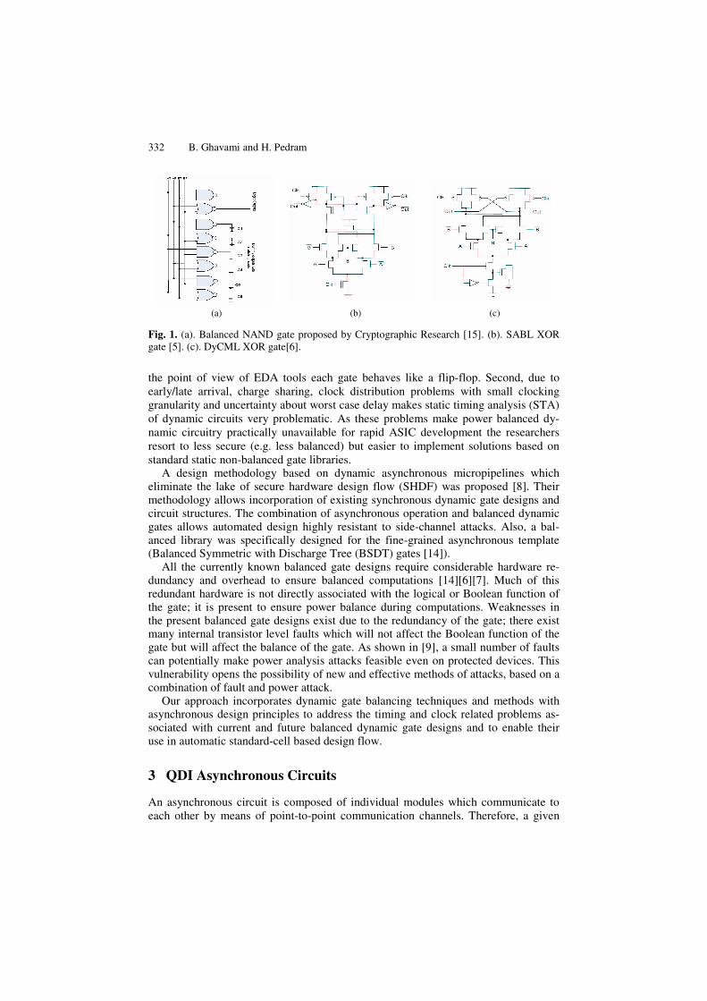
5 Cell-Library Customization
Now we are focused the PCFB power balancing requirements. Our analyzing and simu-lation results show that the function and operation of handshake (control) part of a PCFB template (sec. 4 and 5 in Figure 4) is completely data independent and only the input and output validity checker requires a trivial power balancing consideration which can be easily met with two additional transistors in NAND/NOR gate (Figure 5.(a)) . However, as mentioned in [9], due to the hardware redundancy in balanced gate de-signs, there are many faults making a balanced gate imbalanced without causing logical errors. Due to this redundancy, these faults might not create logical errors and hence would not be detected by traditional voltage level testing and reliability measurements. This vulnerability opens the possibility of new methods of attacks based on a combina-tion of fault and power attacks[9].
To overcome this vulnerability, a better balancing solution can be obtained by us-ing a duplicate NOR gates and a C_Element [12] in input and output validity checker of a PCFB template (Figure 5.(b)). The C_Element’s output changes when both of its inputs have the same value and their values are opposite of the C_Element current value. By nature, a C-element gate is intrinsically balanced. If a fault injected in the proposed balancing circuits that previously mentioned, the circuit creates deadlock (then alarm signal actives). By using this method, when the output must be charged to

336 B. Ghavami and H. Pedram
Fig. 5. (a) Balanced NOR gate [5]. (b) Our enhanced Balanced NOR gate for Input validity checker.
one and when the circuit is fault free, both of the pull-up network’s branches will charge the inputs of the C_Element. As a result the output of the C_Element will be charged to one. But if a fault is injected to one of the pull-up networks branches, the C_Element will not be charged to the new value. Consequently, we will be able to discover the attacker’s injected fault in the logic level and avoid any hybrid Fault Analysis-Deferential Power Attack[9] (DPA/ FI). This method and proposed compu-tational section (for AND/OR/XOR PCFB templates) is the main contribution of our work against DPA/FI.
The computational section is the last module for balancing considerations, and naturally, it is the main source of power imbalance. By using a SABL [5] gate a as the computational section of the PCFB template a QDI balanced gate can be resulted. Asynchronous handshake part removes the clocking and timing difficulties that nor-mally associated with the dynamic gates. Furthermore, enhances their security appli-cations due to the benefits of asynchronous behavior as mentioned in sec.3.
By using a modified SABL [5] gate and employing Discharge Tree (DT) [14] as the computational section of the PCFB template, as shown on the Figure 6, a fully QDI balanced gate results. Using DT results the parasitic capacitors placed in inter-mediate nodes discharging in each evaluation phase. This will results a certain amount of capacitor resistance charging and discharging totally independent of input data. Figure 6 shows the implemented XOR and AND gates in this style. Our simulation results show that the resulted gates balance is approximately 6 times better than the synchronous SABL implementations. Furthermore, the timing and voltage tolerance of the QDI implementation allows for more aggressive dynamic designs which can achieve better balance than previous designs. However, due to redundancy in Dis-charge Tree, some faults might not create logical errors and hence would not be de-tected by traditional voltage level testing and reliability measures. Overcoming this vulnerability, we add a circuit to computational part of the template to detect those faults and generate Alarm-Signal (Figure 6). Alarm-Signal becomes active when a fault occurs in one of the transistors in Discharge Tree and it has employed to cause a pipeline stall which naturally prevents further data processing and creates deadlock within the pipeline. This signal behaves like alarm signal that has been introduced in [11]. The chip alarm signal is resulted from Alarm-Signals of each template which are wired-and together. Because of using Alarm-Signal generator, balancing of our cells is approximately decreased 6.34 %, while compared to BSDT cell library [14], our proposed cell library is resistance against DPA/FI attacks.

An Automatic Design Flow for Implementation of Side Channel 337
Fig. 6. (a) The Balanced AND computational section. (b) The Balanced XOR computational section.
The sequence in asynchronous handshake protocol adds natural fault resistance to the design. Almost all the single stuck-at faults, inside and outside of the complete balanced asynchronous gate, does not have an influence on functionality of the cir-cuits but the system will be stocked in deadlock. That is the faults prevent or stop the necessary of four phase handshake protocol between each gate leads to stalling the communication between dependent downstream gates and preventing any further data processing. Synchronous based balanced dynamic logic gates have no comparable such property. This additional property should make it much harder to use invasive attacks on a circuit since almost all of the tampering would be detected by a pipeline stall. Additional error detection based on other high level fault-tolerant methods can be added easily due to the CSP-specification of the circuit.
6 AES Implementation
To estimate efficiency of proposed methodology, we compare performance of auto-matically synthesized synchronous and asynchronous (with use of proposed balanced cell library) implementation of AES algorithm using TSMC 0.18 technology. The same specification of the AES with 128 key/inputs [22] has been used for both implementations. Synchronous implementation was synthesized with the Artisan Sage-XTM [21] standard cell library using the TSMC 0.18um technology. By using automatically pipelined synchronous implementation, (with Synopsys Design Com-piler – maximum performance setting) – the performance was at the rate 43.69 MHz whereas the performance of our asynchronous implementation exceeds 122.37 MHz.

338 B. Ghavami and H. Pedram
Note that in synchronous case there is no side-channel attacks protection if there was, it would results a significant performance overhead.
We performed a full analysis of the side-channel information leakage from a sam-ple implementation. Initial simulations of power and timing analysis attacks on the Sbox of the AES indicate the benefits of the balanced dynamic gates and QDI asyn-chronous circuits, which are the main goals of our proposed implementations. Also the DFA was applied to the attack performed on our implementation and desirable simulations were resulted. We are currently evaluating whether there is a possibility of weakness resulting from the combination of the countermeasures, but up to this point, none had been found.
7 Conclusion
A fully automated design flow and a set of secure library cells resistant to power analysis and fault injection attacks are introduced for implementation of secure QDI asynchronous circuits. Furthermore, a test methodology to resolve the faults making our templates imbalanced is presented. This methodology would cause the DPA/FI attacks to proposed library cells almost impossible. The results show that our pro-posed cell library is approximately 5.62 times more balanced than the best cells designed using previous synchronous balancing methods.
As mention before, some of the transistor level single stuck-at faults inside and outside of the complete PCFB template can not creates deadlock within the pipeline. Attackers may be motivated by this deficiency in the future, thus we are working to propose PCFB template that 100% of the single stuck-at faults result in pipeline stall.
References
1. Kocher, P., Jaffe, J., Jun, B.: Differential Power Analysis. In: Wiener, M.J. (ed.) CRYPTO 1999. LNCS, vol. 1666, pp. 388–397. Springer, Heidelberg (1999)
2. adn, J.J.Q., Samyde, D.: Side-channel Cryptanalysis. In: Proc. SECI, September 2002, pp. 179–184 (2002)
3. Kocher: Timing Attacks on Implementations of Diffe-Hellman, RSA, DSS and Other Sys-tems. In: Koblitz, N. (ed.) CRYPTO 1996. LNCS, vol. 1109, pp. 104–113. Springer, Hei-delberg (1996)
4. Quisquater, J.J., Samyde, D.: ElectroMagnetic Analysis (EMA): Measures and Counter-measures for Smart Cards. In: Wiener, M.J. (ed.) CRYPTO 1999. LNCS, vol. 1666, Springer, Heidelberg (1999)
5. Tiri, K., Akmal, M., Verbauwhede, I.: A Dynamic and Differential CMOS Logic with Signal Independent Power Consumption to Withstand Differential Power Analysis on Smart Cards. In: 28th European Solid-State Circuits Conference (ESSCIRC 2002), Sep-tember 2002, pp. 403–406 (2002)
6. Mace, F., Standaert, F.X., Quisquater, J.J., Legat, J.D.: A Design Methodology for Se-cured ICs Using Dynamic Current Mode Logic. In: Paliouras, V., Vounckx, J., Verkest, D. (eds.) PATMOS 2005. LNCS, vol. 3728, pp. 550–560. Springer, Heidelberg (2005)

An Automatic Design Flow for Implementation of Side Channel 339
7. Tiri, K., Verbauwhede, I.: A Logic Level Design Methodology for a Secure DPA Resistant ASIC or FPGA Implementation. In: Tiri, K. (ed.) Design, Automation and Test in Europe Conference (DATE 2004), February 2004, pp. 246–251 (2004)
8. Kulikowski, K., Smirnov, A., Taubin, A.: Automated Design of Cryptographic Devices Resistant to Multiple Side-Channel Attacks. In: Goubin, L., Matsui, M. (eds.) CHES 2006. LNCS, vol. 4249, Springer, Heidelberg (2006)
9. Kulikowski, K., Karpovsky, M., Taubin, A.: DPA on faulty cryptographic hardware and countermeasures. In: Fault Diagnosis and Tolerance in Cryptography. 3nd International Workshop (2006)
10. Kulikowski, K., Karpovsky, M., Taubin, A.: Robust Codes for Fault Attack Resistant Cryptographic Hardware. In: Fault Diagnosis and Tolerance in Cryptography, 2nd Interna-tional Workshop, Edinburgh (2005)
11. Bouesse, F., Fesquet, L., Renaudin, M.: QDI circuit to Improve Smartcard Security. In: 2nd Asynchronous Circuit Design Workshop (ACID2002), Munich, Germany, Januray 2002, pp. 28–29 (2002)
12. Renaudin, M.: Asynchronous circuits and systems: a promising design alternative. Micro-electronic for Telecommunications: managing high complexity and mobility (MIGAS 2000), Guest Editors : Senn, P., Renaudin, M., Boussey, J. Special issue of the Microelec-tronics-Engineering Journal 54(1-2), 133–149 (2000)
13. Biham, E., Shamir, A.: Differential fault analysis of secret key cryptosystems. In: Kaliski Jr., B.S. (ed.) CRYPTO 1997. LNCS, vol. 1294, pp. 513–525. Springer, Heidelberg (1997)
14. MacDonald, D.J.: A Balanced-Power Domino-Style Standard Cell Library for Fine-Grain Asynchronous Pipelined Design to Resist Differential Power Analysis Attacks. Master of Science Thesis, 2005, Boston University, Boston (2005), availabe at http://reliable.bu.edu/Projects/ MacDonald_thesis.pdf
15. Jaffe, J., Kocher, P., Jun, B.: Hardware-level mitigation and DPA countermeasures for Cryptographic devices, US Patent 6654884
16. http://www.asynch.ir/persia 17. Seifhashemi, A., Pedram, H.: Verilog HDL, Powered by PLI: a Suitable Framework for
Describing and Modeling Asynchronous Circuits at All Levels of Abstraction. In: Proc. Of 40th DAC, June 2003, Anneheim, CA, USA (2003)
18. Sparso, J., Furber, S.: Principles of Asynchronous Circuit Design – A System Perspective. Kluwer Academic Publishers (2002)
19. McCardle, J., Chester, D.: Measuring an asynchronous processor’s power and noise. In: SNUG (2001)
20. Martin, A.J.: Synthesis of Asynchronous VLSI Circuits, Caltech, CS-TR-93-28 (1991) 21. TSMC 0.18μm process 1.8-volt Sage-X standard cell library databook (September 2003) 22. Fips pub 197: Advanced encryption standard, http://csrc.nist.gov