AN ALGORITHM TO GROUP DEFECTS ON PRINTED CIRCUIT BOARD FOR
10
NOOR KHAFIFAH KHALID et. al: AN ALGORITHM TO GROUP DEFECTS ON PCB IJSSST, Vol. 9, No. 2, May 2008 ISSN: 1473-804x online, 1473-8031 print AN ALGORITHM TO GROUP DEFECTS ON PRINTED CIRCUIT BOARD FOR AUTOMATED VISUAL INSPECTION NOOR KHAFIFAH KHALID, ZUWAIRIE IBRAHIM, and MOHAMAD SHUKRI ZAINAL ABIDIN Faculty of Electrical Engineering, Centre for Artificial Intelligence and Robotics (CAIRO), Universiti Teknologi Malaysia, 81310 UTM Skudai, Johor, MALAYSIA e-mail:[email protected], [email protected], [email protected] http://blog.fke.utm.my/~zuwairie Abstract: Due to disadvantages in manual inspection, an automated visual inspection system is needed to eliminate subjective aspects and provides fast and quantitative assessment of printed circuit board (PCB). Up to the present, there has been a lot of work and research concentrated on PCB defect detection. PCB defects detection is necessary for verification of the characteristics of PCB to make sure it is in conformity with the design specifications. However, besides the need to detect the defects, it is also essential to classify these defects so that the source of these defects can be identified. Unfortunately, this area has been neglected and not been given enough attention. Hence, this study proposes an algorithm to group the defects found on bare PCB. Using a synthetically generated PCB image, the algorithm is able to group 14 commonly known PCB defects into five groups. The proposed algorithm includes several image processing operations such as image subtraction, image adding, logical XOR and NOT, and flood fill operator. Keywords: printed circuit board, defects detection, automated visual inspection. 1 INTRODUCTION During the manufacturing of printed circuit boards, widths of insulators and conductors can change because of manufacturing defects such as dust, overetching, underetching, and spurious metals. The objective of printed circuit board (PCB) inspection is to verify that the characteristics of board manufacturing are in conformity with the design specifications [Mesbahi and Chaibi, 1993]. For many years, human operators are employed to inspect PCB and monitor the results of more than 50 process steps of PCB fabrications. As PCBs normally contain complex and detailed patterns, manual visual inspection is very tiring and very subjective to errors. Furthermore, manual inspection is slow, costly, and can leads to excessive scrap rates. Besides, it also does not assure high quality of inspection. The technology of computer vision has been highly developed and used in several industry applications. One of these applications is the automatic visual inspection of PCB. The automatic visual inspection is important because it removes the subjective aspects and provides fast and quantitative assessments. It also relieve human operator from tedious, boring, and repetitive tasks of inspection. On the other hand, automatic systems do not get tired and are consistent [Moganti et al, 1996]. In general, PCB inspection can be divided into three categories: reference comparison approach, design rule checking (non-referential) approach, and hybrid approach. The reference comparison approach is based on a comparison between the image of the PCB to be tested and that of an ideal PCB which is conform to pre-defined design specifications. There are two major techniques: image comparison methods and model-based inspection. Image comparison, which is the simplest approach, consists of comparing both images pixel-by-pixel using simple logic operators such as XOR. The main difficulty found in these techniques is determining a precise alignment of the reference image and the test image, which makes its utilization difficult. More sophisticated proposals under the same idea, involve feature and template matching [Moganti et al, 1996], but suffer from the same problem and normally require a large number of templates. Model-based methods are techniques, which match the pattern under inspection with a set of predefined models. They are also called Graph-Matching Methods [Moganti et al, 1996] and are based on the structural, topological, and geometrical properties of the image. The major difficulty of those methods is related to the matching complexity. Although Sun
Transcript of AN ALGORITHM TO GROUP DEFECTS ON PRINTED CIRCUIT BOARD FOR

NOOR KHAFIFAH KHALID et. al: AN ALGORITHM TO GROUP DEFECTS ON PCB
IJSSST, Vol. 9, No. 2, May 2008 ISSN: 1473-804x online, 1473-8031 print
AN ALGORITHM TO GROUP DEFECTS ON PRINTED
CIRCUIT BOARD FOR AUTOMATED VISUAL
INSPECTION
NOOR KHAFIFAH KHALID, ZUWAIRIE IBRAHIM, and MOHAMAD SHUKRI
ZAINAL ABIDIN
Faculty of Electrical Engineering, Centre for Artificial Intelligence and Robotics (CAIRO),
Universiti Teknologi Malaysia,
81310 UTM Skudai, Johor, MALAYSIA
e-mail:[email protected], [email protected], [email protected]
http://blog.fke.utm.my/~zuwairie
Abstract: Due to disadvantages in manual inspection, an automated visual inspection system is needed to
eliminate subjective aspects and provides fast and quantitative assessment of printed circuit board (PCB). Up to
the present, there has been a lot of work and research concentrated on PCB defect detection. PCB defects
detection is necessary for verification of the characteristics of PCB to make sure it is in conformity with the
design specifications. However, besides the need to detect the defects, it is also essential to classify these defects
so that the source of these defects can be identified. Unfortunately, this area has been neglected and not been
given enough attention. Hence, this study proposes an algorithm to group the defects found on bare PCB. Using
a synthetically generated PCB image, the algorithm is able to group 14 commonly known PCB defects into five
groups. The proposed algorithm includes several image processing operations such as image subtraction, image
adding, logical XOR and NOT, and flood fill operator.
Keywords: printed circuit board, defects detection, automated visual inspection.
1 INTRODUCTION
During the manufacturing of printed circuit boards,
widths of insulators and conductors can change
because of manufacturing defects such as dust,
overetching, underetching, and spurious metals. The
objective of printed circuit board (PCB) inspection is
to verify that the characteristics of board
manufacturing are in conformity with the design
specifications [Mesbahi and Chaibi, 1993].
For many years, human operators are employed to
inspect PCB and monitor the results of more than 50
process steps of PCB fabrications. As PCBs
normally contain complex and detailed patterns,
manual visual inspection is very tiring and very
subjective to errors. Furthermore, manual inspection
is slow, costly, and can leads to excessive scrap
rates. Besides, it also does not assure high quality of
inspection.
The technology of computer vision has been highly
developed and used in several industry applications.
One of these applications is the automatic visual
inspection of PCB. The automatic visual inspection
is important because it removes the subjective
aspects and provides fast and quantitative
assessments. It also relieve human operator from
tedious, boring, and repetitive tasks of inspection.
On the other hand, automatic systems do not get
tired and are consistent [Moganti et al, 1996].
In general, PCB inspection can be divided into three
categories: reference comparison approach, design
rule checking (non-referential) approach, and hybrid
approach.
The reference comparison approach is based on a
comparison between the image of the PCB to be
tested and that of an ideal PCB which is conform to
pre-defined design specifications. There are two
major techniques: image comparison methods and
model-based inspection.
Image comparison, which is the simplest approach,
consists of comparing both images pixel-by-pixel
using simple logic operators such as XOR. The main
difficulty found in these techniques is determining a
precise alignment of the reference image and the test
image, which makes its utilization difficult. More
sophisticated proposals under the same idea, involve
feature and template matching [Moganti et al, 1996],
but suffer from the same problem and normally
require a large number of templates.
Model-based methods are techniques, which match
the pattern under inspection with a set of predefined
models. They are also called Graph-Matching
Methods [Moganti et al, 1996] and are based on the
structural, topological, and geometrical properties of
the image. The major difficulty of those methods is
related to the matching complexity. Although Sun
1

NOOR KHAFIFAH KHALID et. al: AN ALGORITHM TO GROUP DEFECTS ON PCB
IJSSST, Vol. 9, No. 2, May 2008 ISSN: 1473-804x online, 1473-8031 print
and Tsai [Sun and Tsai, 1993] proposed a technique
called Pattern Attributed Hypergraph to make the
method more practical, it still remains a complex
and time-consuming method.
The design rule checking approach is based on the
verification of the general design rules that is
essential in the verification of the widths of
conductors and insulators. As a kind of automatic
inspection algorithm for bare PCB, the design rule
checking has been proposed and well known to the
automatic visual inspection system manufacturers
[Hong et al, 1998].
The design rule checking (DRC) method checks if
all patterns and spaces of PCB surface meet or
violate common knowledge, which is called the
design rule. Because a simple algorithm is applied
directly to an image, the implementation of this
algorithm is comparatively easy. This means that it
does not require severe alignment and adjustment of
a mechanical part to get a non-distorted image.
However, this method is a very time consuming
process and a great computing power is needed to
meet user’s requirement of inspection time.
Nowadays, considering the state of affairs of an
inspection system, the combined inspection methods
are used. This hybrid approach merges the
advantages of the reference comparison method and
the DRC method to overcome the weaknesses of
each method. For example, most of the design-rule
verification methods are limited to verifying
minimum conductor trace, angular errors, and
spurious copper.
Then, PCB defects which do not violate the design
rules are detected by reference comparison methods.
These methods can detect missing features or
extraneous features. The design rule process detects
all defects within small and medium features while
the comparison methods are sensitive to the largest
features. Hybrid approach makes use both of these
methods as they complement each other and
therefore achieve a full sensitivity of PCB
inspection.
From the literature review, it is found that only Wu
[Wu et al, 1996] and Heriansyah [Heriansyah, 2004]
carried out the defects classification of PCB. The
other algorithms concentrated only on PCB defects
detection. In defect detection, the type of defects is
not important. However, in defects classification, the
types of each defect need to be obtained.
Firstly, Wu [Wu et al, 1996] developed PCB defects
classification based on pixel processing operation.
The method is divided into two stages: defect
detection and defects classification. Defect detection
stage is accomplished using subtraction procedure
while the second stage is completed using three
indices: the type of object detected, the difference in
object numbers, and the difference in background
numbers between the inspected image and the
template.
Secondly, Heriansyah [Heriansyah, 2004] developed
an algorithm using the advantages of artificial neural
network to correctly classify defective PCB patterns.
Binary morphological image processing concept and
Learning Vector Quantization (LVQ) are employed
in this algorithm. The morphological operations such
as erosion, dilation, opening, and closing are used to
segment PCB image into basic primitive patterns.
The LVQ neural network, which consists of input,
competitive layer as the first layer (hidden layer),
and linear layer as the second layer (or output layer),
has been selected as the classifier for the proposed
technique to classify the defects that could occur on
the PCB. This type of neural network has been
chosen because of its ability to converge based on
the training set available.
2 DEFECTS
There are some defects commonly found on PCB.
Conductor breaking and short-circuit are
characterized as fatal defects. Pinhole, breakout,
overetch, and underetch are characterized as
potential defects. Fatal defects are those in which the
PCB does not attend the objective they are designed
for, and potential defects are those compromising
the PCB during their utilization [Tatibana et al,
1997].
During etching process, the anomalies occurring on
bare PCB could be largely classified in two
categories: the one is excess of copper and the other
one is missing copper. The incomplete etching
process leaves unwanted conductive materials and
forms defects like short, extra hole, protrusion,
island, and small space. The excessive etching
makes open, pin hole, nick (mouse bite), and thin
pattern. In addition to the defects mentioned above,
some other defects may exist on bare PCB, for
example, missing holes (due to tool break), scratch
(due to handling mistake), and cracks.
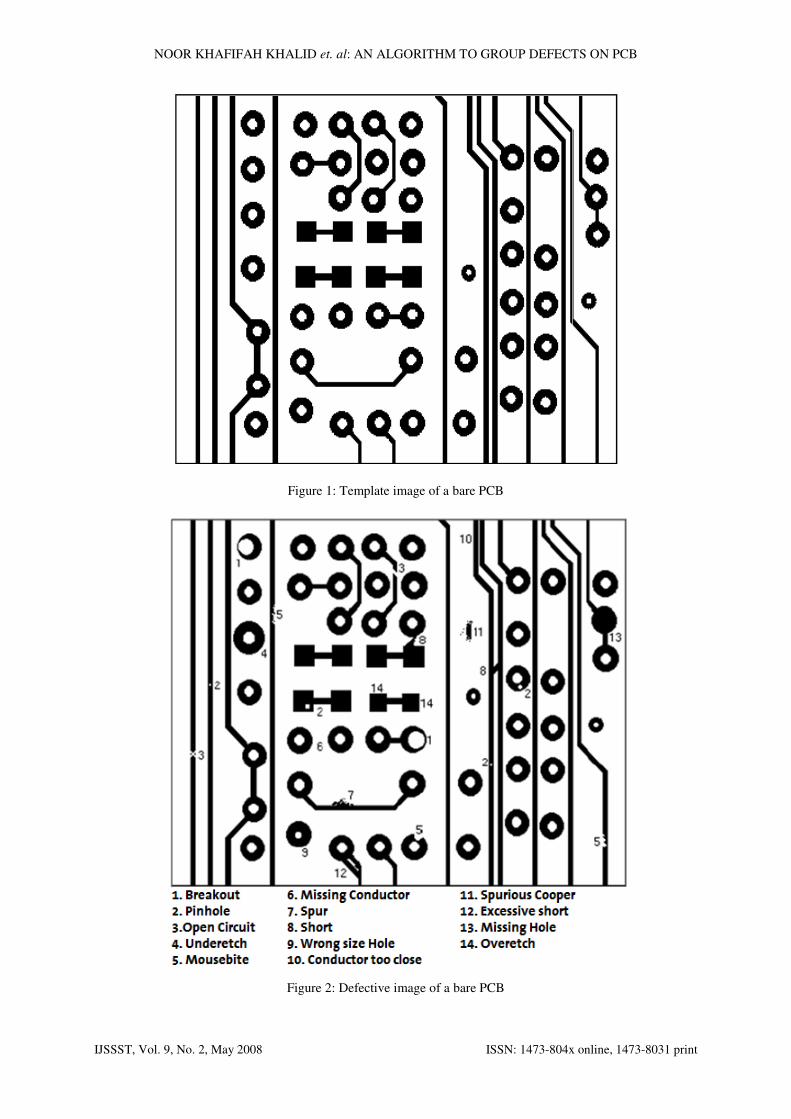
Figure 1 and Figure 2 show the examples of defect
free PCB image and defective image, respectively.
Though each defect shown in the Figure 2 is a
representative example of certain defects, the shape
and the size of the defects may vary from one
occurrence to another.
2
NOOR KHAFIFAH KHALID
IJSSST, Vol. 9, No. 2, May 2008
KHALID et. al: AN ALGORITHM TO GROUP DEFECTS ON PCB
ISSN: 1473-804x online, 1473
Figure 1: Template image of a bare PCB
Figure 2: Defective image of a bare PCB
: AN ALGORITHM TO GROUP DEFECTS ON PCB
804x online, 1473-8031 print
3

NOOR KHAFIFAH KHALID et. al: AN ALGORITHM TO GROUP DEFECTS ON PCB
IJSSST, Vol. 9, No. 2, May 2008 ISSN: 1473-804x online, 1473-8031 print
In recent years, the pattern width and space become
smaller and smaller to increase the integration rate
of electrical components per unit area of PCB. This
means the size of defect is also minute and actually
may be less than 30 micron. These defects are not
easily detected by the human eyes and would take
too much inspection time. For this reason, an
automatic visual inspection system is needed.
3 METHODOLOGIES
3.1 Image difference operation
Image difference, which is the simplest technique,
consists of comparing both images pixel-by-pixel by
XOR logic operator. The operation is also called as
image comparison operation. The truth table of XOR
is given in Table 1.
Image difference operation is developed in order to
get the differences between two images. Most likely,
in this study, the images are the template image and
the defective image. The method compares these
two images and the results obtained are the defects
as shown in Figure 3.
3.2 NOT operator
NOT operator is normally used to change an image
from black to white and vice versa. This operator
inverts the bit values of any variable and sets the
corresponding bit according to Table 2. As a result,
the image is changed from black to white and vice
versa as shown in Figure 4 and Figure 5.
3.3 Flood-fill operator
The flood-fill operator changes the colour of a
region, given an initial pixel in that region on binary
and grayscale images. For binary images, flood-fill
operator changes connected background pixels to
foreground pixels until it reaches object boundaries.
This operation could be useful in removing
irrelevant artefacts from images. In this study, this
operator is used to fill the holes in a binary image.
For example, Figure 6 and Figure 7 show the effect
of flood-fill operator on a binary image.
A hole is a set of background pixels that cannot be
reached by filling in the background from the edge
of the image. By default, flood-fill uses 4-connected
neighbours for 2-D inputs and 6-connected
background neighbours for 3-D inputs. For example,
the simplest algorithm for the flood-fill operator is as
the following [Jaime Silvela and Javier Portillo,
2001]:
FLOOD-FILL-1 (initial-pixel,
Initial-colour, final-colour)
colour (initial-pixel) final-colour
Table 1: Truth table of XOR logic operator
Bit 1 Bit 2 Output
0 0 0
0 1 1
1 0 1
1 1 0
Table 2: NOT truth table
Input Output
1 0
0 1
for each n ϵ Neighbours (initial-pixel)
if colour(n) = initial-colour FLOOD-FILL-1 (n, Initial-colour,
final-colour).
The input for this algorithm is an image before
flood-fill operation and the output is the image after
flood-fill operation. This image will be used in
image difference or subtraction operations for defect
detection. The parameters used are the initial pixel,
initial colour, and final colour. If a hole with white
fill and black pixels as boundaries are used as the
input, the initial pixel is located in the hole with
white as the initial colour. Then, the final colour is
black, same as the colour of the hole’s boundaries.
After the algorithm is executed, the white fill of the
hole is changed to black pixel. The output is no
longer a hole, because the hole is filled with the
black pixel.
3.4 Image Subtraction
Image subtraction method used the concept of
simple subtraction and rule as shown in Table 3. In
this work, both images of template image and
defective image are compared pixel by pixel. The
subtract operation produces either negative or
positive pixel value. Therefore, the outcome of this
operation is divided into negative image and positive
image.
3.5 Image addition
Image addition is a method for combining objects in
two images into one image. In this paper, this
operator combines the defects from one group with
the defects from another group in one image. This is
possible using OR logic operator. For 2 inputs 2-bit
data, the truth table of OR is given in Table 4.
3.6 The proposed algorithm
Five algorithms shown in Figure 8 to Figure 12 are
developed to detect and classify the defects into five
groups. Those groups with the respective defects are
as follows:
4
NOOR KHAFIFAH KHALID
IJSSST, Vol. 9, No. 2, May 2008
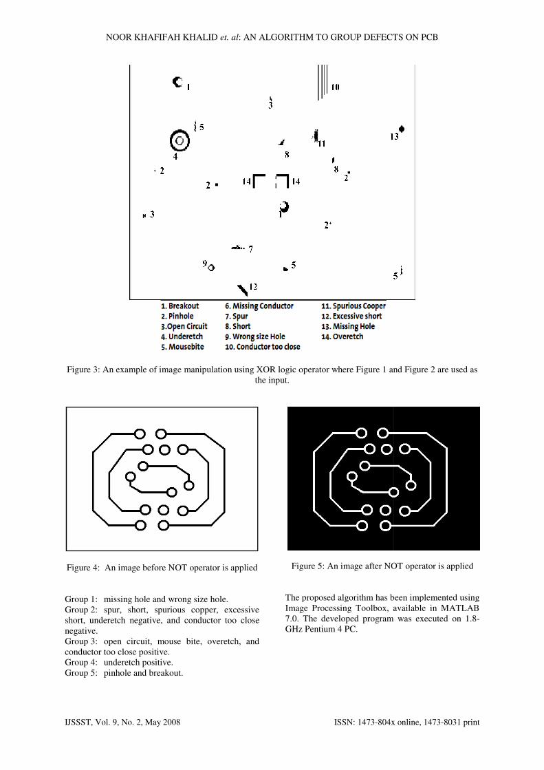
Figure 3: An example of image manipulation using XOR logic operator
Figure 4: An image before NOT operator is applied
Group 1: missing hole and wrong size hole
Group 2: spur, short, spurious copper, excessive
short, underetch negative, and conductor too close
negative.
Group 3: open circuit, mouse bite, overetch
conductor too close positive.
Group 4: underetch positive.
Group 5: pinhole and breakout.
KHALID et. al: AN ALGORITHM TO GROUP DEFECTS ON PCB
ISSN: 1473-804x online, 1473
An example of image manipulation using XOR logic operator where Figure 1 and Fig
the input.
mage before NOT operator is applied
missing hole and wrong size hole.
, short, spurious copper, excessive
and conductor too close
open circuit, mouse bite, overetch, and
Figure 5: An image after NOT operator is applied
The proposed algorithm has been implemented using
Image Processing Toolbox, available in MATLAB
7.0. The developed program was executed on 1.8
GHz Pentium 4 PC.
: AN ALGORITHM TO GROUP DEFECTS ON PCB
804x online, 1473-8031 print
1 and Figure 2 are used as
mage after NOT operator is applied
The proposed algorithm has been implemented using
sing Toolbox, available in MATLAB
7.0. The developed program was executed on 1.8-
5

NOOR KHAFIFAH KHALID et. al: AN ALGORITHM TO GROUP DEFECTS ON PCB
IJSSST, Vol. 9, No. 2, May 2008 ISSN: 1473-804x online, 1473-8031 print
Figure 6: An image before flood-fill operator is
applied
Figure 7: An image after flood-fill operator is
applied
Table 3: Two rules for image subtraction
Rule Result
If 1 - 0 = 1 Positive pixel image
If 0 - 1 = -1 Negative pixel image
Table 4: The truth table of OR logic operator
Bit 1 Bit 2 Output
0 0 0
0 1 1
1 0 1
1 1 1
5 RESULTS AND DISCUSSION
Based on the algorithms shown in Figure 8 to Figure
12, these algorithms need two images, namely
template image and defective image. In this paper,
these algorithms use Figure 1 as template image and
Figure 2 as defective image.
At first, both images are subjected to image
subtraction operation to produce negative image and
positive image. Then, NOT operator and flood-fill
operator are applied to template image and the
defective image separately to produce A1 and A2
images, respectively. From there, the algorithms
continue to produce the results. The results shown
will be based on these images.
5.1 Group 1
The algorithm shown in Figure 8 produces two types
of defects. These defects are missing hole and wrong
size hole, as shown in Figure 13. These defects are
obtained after image subtraction operation is applied
between A1 image and negative image.
5.2 Group 2
The negative image initially consist of eight types of
defects including the defects in Group 1, which are
missing hole and wrong size hole. As shown in
Figure 9, in order to eliminate those defects in
Group 1 from negative image, image difference
operation is applied between the negative image and
Group 1 image to produce Group 2 image. Group 2
consists of six types of defects: spur, short, spurious
copper, excessive short, underetch negative, and
conductor too close negative, as shown in Figure 14.
5.3 Group 3
Initially, positive image consists of seven types of
defects including the defects in A3 image. As shown
in Figure 10, in order to eliminate those defects in
A3 from the positive image, image difference
operation is applied between positive image and A3
to produce Group 3. As a result, Group 3 consists of
four types of defects: open circuit, mouse bite,
overetch, and conductor too close positive, as shown
in Figure 15.
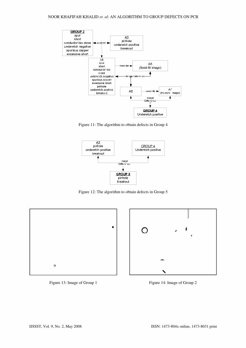
5.4 Group 4
By combining Group 2 and A3 image, the defects
from both images are combined in an image, namely
A4 image. A4 image consist of nine defects from A3
and from Group 2. A4 image is then subjected to
flood-fill operator and A5 image is produced. As
shown in Figure 11, by comparing A4 and A5
images using image difference operator, A6 image is
obtained. Then, A7 image is obtained after flood-fill
operator is applied to A6 image. Similarly, Group 4
image, which shows only underetch positive defect
is produced as shown in Figure 16.
6

NOOR KHAFIFAH KHALID et. al: AN ALGORITHM TO GROUP DEFECTS ON PCB
IJSSST, Vol. 9, No. 2, May 2008 ISSN: 1473-804x online, 1473-8031 print
Figure 8: The algorithm to obtain defects in Group 1
Figure 9: The algorithm to obtain defects in Group 2
Figure 10: The algorithm to obtain defects in Group 3
5.5 Group 5
Initially, A3 image is obtained by applying image
subtraction operator between the positive image and
A2 image. The A3 image consists of three defects:
pinhole, underetch positive, and breakout. As defects
from Group 4 have been obtained previously, those
defects should be taken out from A3 image.
Therefore, image difference operator is again
employed between Group 4 image and A3 image to
produce Group 5 image. Group 5 image consist of
two defects (pinhole and breakout) as shown in
Figure 17.
7
NOOR KHAFIFAH KHALID et. al: AN ALGORITHM TO GROUP DEFECTS ON PCB
IJSSST, Vol. 9, No. 2, May 2008 ISSN: 1473-804x online, 1473-8031 print
Figure 11: The algorithm to obtain defects in Group 4
Figure 12: The algorithm to obtain defects in Group 5
Figure 13: Image of Group 1
Figure 14: Image of Group 2
8

NOOR KHAFIFAH KHALID et. al: AN ALGORITHM TO GROUP DEFECTS ON PCB
IJSSST, Vol. 9, No. 2, May 2008 ISSN: 1473-804x online, 1473-8031 print
Figure 15: Image of Group 3
Figure 16: Image of Group 4
Figure 17: Image of Group 5
6 CONCLUSION
As a conclusion, the proposed algorithm can be
implemented on bare PCB to identify and to group
PCB defects. However, the major limitation of this
algorithm is that the proposed algorithm is
developed to work with binary images only, whereas
the output from the cameras is in grayscale format
[Heriansyah, 2004]. Although the conversion can be
made from grayscale to binary format imperfection
still can be occurred. Thus, this algorithm should be
improved to handle the grayscale image format.
Also, during the computation of defect detection and
implementation, this operation brings along the
unwanted noise due to misalignment and uneven
binarization. Thus, in order to improve the
algorithm, unwanted noise should be considered.
Since the proposed algorithm, at the moment, is only
able to separate 14 types of defects into five groups,
therefore, it is highly suggested that the algorithm
should be improved to achieve better result, which is
to classify all the 14 types of defects separately.
ACKNOWLEDGMENT
This work was supported by the Ministry of Higher
Education (MOHE), Malaysia, through Fundamental
Research Grant Scheme (FRGS), Vot 78226. The
authors would like to express their gratitude to
MOHE and the Universiti Teknologi Malaysia for
providing good research atmosphere and high-end
facilities, hence make this work run smoothly.
REFERENCES
Ji-joong Hong, Kyung-ja Park and Kyung-gu Kim
1998, “Parallel processing machine vision system
for bare PCB inspection”, Industrial Electronics
Society, IECON ’98. Proceedings of the 24th Annual
Conference of the IEEE. Vol 3, pp. 1346 – 1350.
J. E. Mesbahi and M. Chaibi 1993, “Printed Circuit
Boards Inspection Using Two New Algorithms of
Dilation and Connectivity Preserving Shrinking”,
Proceedings of the 1993 IEEE-SP Workshop on
Neural Networks for Processing, pp. 527 – 536.
Jaime Silvela and Javier Portillo. 2001, “Breadth-
First Search and Its Application To Image
Processing Problems”, IEEE Transactions On Image
Processing, Vol. 10, No. 8, pp. 1194 – 1199.
Lampinen, J.,Laaksonen, J., and Oja, E. 1997,
“Neural Network Systems, Techniques and
Applications in Pattern Recognition”, Technical
Report B1, Laboratory of Computational
Engineering, Helsinki University of Technology.
Moganti, M., Ercal, F., Dagli, C. H. and Shou,
Tsunekawa 1996, “Automatic PCB Inspection
Algorithms: A Survey”, Computer Vision and Image
Understanding, Vol. 63, No.2, pp. 287 – 313.
Rudi Heriansyah 2004, “Classification of Defects
On Bare PCB Using Neural Network Technique,”
University Technology Malaysia: Master
Dissertation.
9
NOOR KHAFIFAH KHALID
IJSSST, Vol. 9, No. 2, May 2008
Stader, J. 1988, “Applying Neural Networks”,
Proceedings of International Conference on Neural
Networks. 2: 451 – 459.
Tatibana, M.H., Lotufo, R. de A.
Automatic PCB Inspection Technique Based on
Connectivity”, Computer Graphics and Image
Processing Proceedings, X Brazilian Symposium
pp. 187 – 194.
W.Y. Wu, M.J.J. Wang, and C.M. Liu
“Automated inspection of printed
through machine vision,” Comput. Ind
pp.103 – 111.
Yung-Nien Sun, and Ching Tsorng Tsai
New Model-Based Approach for Indusrial Visual
Inspection”, Pattern Recognition, Vol.
pp.1327 – 1336.
AUTHOR BIOGRAPHIES
NOOR KHAFIFAH KHALID
Perak, Malaysia
received the B.Eng
electrical engineering from
Universiti Teknologi
Malaysia, Johor, M
in 2007. Sh
pursuing her
in the Faculty of Electrical
Engineering, Universiti
Teknologi Malaysia, Johor, Malaysia. Her research
interest includes image processing, DNA computing
and computational intelligence.
KHALID et. al: AN ALGORITHM TO GROUP DEFECTS ON PCB
ISSN: 1473-804x online, 1473
Stader, J. 1988, “Applying Neural Networks”,
Proceedings of International Conference on Neural
Lotufo, R. de A. 1997, “Novel
PCB Inspection Technique Based on
er Graphics and Image
lian Symposium,
W.Y. Wu, M.J.J. Wang, and C.M. Liu. 1996,
printed circuit boards
Comput. Ind., Vol. 28,
Nien Sun, and Ching Tsorng Tsai. 1992, “A
h for Indusrial Visual
, Vol. 25, No.11,
NOOR KHAFIFAH was born in
Perak, Malaysia. She
received the B.Eng in
electrical engineering from
i Teknologi
, Johor, Malaysia
She is currently
her master degree
in the Faculty of Electrical
Engineering, Universiti
ologi Malaysia, Johor, Malaysia. Her research
DNA computing,
ZUWAIRIE IBRAHIM
holds B.Eng.
from
Malaysia
respectively.
PhD
from Meiji University,
Japan
author/co
than
national/international journals
research interests include DNA computing
intelligence as well as image processing, particularly
in automated visual inspection for industrial
applications.
: AN ALGORITHM TO GROUP DEFECTS ON PCB
804x online, 1473-8031 print
ZUWAIRIE IBRAHIM
holds B.Eng. and M.Eng.
Universiti Teknologi
Malaysia, in 2000 and 2002,
respectively. He received his
in DNA computing
from Meiji University,
Japan, in 2006. He is an
author/co-author of more
50 publications in
ernational journals and conferences. His
include DNA computing, swarm
image processing, particularly
visual inspection for industrial
10