An Advanced Time Averaging Modelling Technique … · Abstract An Advanced Time Averaging Modelling...
104
An Advanced Time Averaging Modelling Technique for Power Electronic Circuits by Goce Jankuloski A thesis submitted in conformity with the requirements for the degree of Master of Applied Science Graduate Department of Electrical Engineering University of Toronto c ⃝ Copyright 2014 by Goce Jankuloski
Transcript of An Advanced Time Averaging Modelling Technique … · Abstract An Advanced Time Averaging Modelling...
An Advanced Time Averaging Modelling Technique forPower Electronic Circuits
by
Goce Jankuloski
A thesis submitted in conformity with the requirementsfor the degree of Master of Applied Science
Graduate Department of Electrical EngineeringUniversity of Toronto
c⃝ Copyright 2014 by Goce Jankuloski

Abstract
An Advanced Time Averaging Modelling Technique for Power Electronic Circuits
Goce Jankuloski
Master of Applied Science
Graduate Department of Electrical Engineering
University of Toronto
2014
For stable and efficient performance of power converters, a good mathematical model
is needed. This thesis presents a new modelling technique for DC/DC and DC/AC
Pulse Width Modulated (PWM) converters. The new model is more accurate than the
existing modelling techniques such as State Space Averaging (SSA) and Discrete Time
Modelling. Unlike the SSA model, the new modelling technique, the Advanced Time
Averaging Model (ATAM) includes the averaging dynamics of the converter’s output. In
addition to offering enhanced model accuracy, application of linearization techniques to
the ATAM enables the use of conventional linear control design tools. A controller design
application demonstrates that a controller designed based on the ATAM outperforms one
designed using the ubiquitous SSA model. Unlike the SSA model, ATAM for DC/AC
augments the system’s dynamics with the dynamics needed for subcycle fundamental
contribution (SFC) calculation. This allows for controller design that is based on an
exact model.
ii

Acknowledgements
This thesis would not have been possible without the support and mentorship from my
supervisor, Peter W. Lehn. A lot of meetings, work and discussion went into this thesis.
He was always helpful, supportive, and understanding. It was a great learning experience
and unique to have the opportunity to learn from him.
I’d also like to thank my family, for the overwhelming support they have given me over
my whole education, especially these past two years. It means a lot for me to culminate
my Masters’ study with this thesis, which I consider my best work to date.
iii

Contents
1 Introduction 1
1.1 Background . . . . . . . . . . . . . . . . . . . . . . . . . . . . . . . . . . 1
1.2 Literature Review . . . . . . . . . . . . . . . . . . . . . . . . . . . . . . . 5
1.3 Thesis Objectives . . . . . . . . . . . . . . . . . . . . . . . . . . . . . . . 9
2 Converter Modelling 11
2.1 Average Modelling . . . . . . . . . . . . . . . . . . . . . . . . . . . . . . 11
2.2 SSA Modelling Inaccuracy . . . . . . . . . . . . . . . . . . . . . . . . . . 16
2.2.1 Example . . . . . . . . . . . . . . . . . . . . . . . . . . . . . . . . 17
2.3 SSA Implementation Inaccuracy . . . . . . . . . . . . . . . . . . . . . . . 19
2.4 Summary . . . . . . . . . . . . . . . . . . . . . . . . . . . . . . . . . . . 24
3 DC/DC Modelling 26
3.1 Sliding Window Average . . . . . . . . . . . . . . . . . . . . . . . . . . . 27
3.1.1 Elimination of the Delayed Integrator State . . . . . . . . . . . . 32
3.2 ATAM Application Example . . . . . . . . . . . . . . . . . . . . . . . . . 33
3.3 Validation . . . . . . . . . . . . . . . . . . . . . . . . . . . . . . . . . . . 35
3.4 Summary . . . . . . . . . . . . . . . . . . . . . . . . . . . . . . . . . . . 35
4 DC/DC Model Linearization and Control 38
4.1 Linearization . . . . . . . . . . . . . . . . . . . . . . . . . . . . . . . . . 39
iv

4.2 Model Demonstration . . . . . . . . . . . . . . . . . . . . . . . . . . . . . 42
4.2.1 Open Loop Performance . . . . . . . . . . . . . . . . . . . . . . . 42
4.2.2 Closed Loop Performance . . . . . . . . . . . . . . . . . . . . . . 44
4.3 Summary . . . . . . . . . . . . . . . . . . . . . . . . . . . . . . . . . . . 49
5 DC/AC Modelling 50
5.1 Modelling Challenges . . . . . . . . . . . . . . . . . . . . . . . . . . . . . 51
5.2 Subcycle Fundamental Contribution . . . . . . . . . . . . . . . . . . . . . 52
5.2.1 Modifying SFC States to Memoryless . . . . . . . . . . . . . . . . 55
5.3 Two Phase Inverter Modelling . . . . . . . . . . . . . . . . . . . . . . . . 59
5.3.1 Decoupled Fourier Transform . . . . . . . . . . . . . . . . . . . . 60
5.4 Model Demonstration . . . . . . . . . . . . . . . . . . . . . . . . . . . . . 68
5.4.1 Pure Sine Wave . . . . . . . . . . . . . . . . . . . . . . . . . . . . 70
5.4.2 Oscillator with Negative Sequence . . . . . . . . . . . . . . . . . . 72
5.5 Summary . . . . . . . . . . . . . . . . . . . . . . . . . . . . . . . . . . . 73
6 Conclusion 76
6.1 Future Work . . . . . . . . . . . . . . . . . . . . . . . . . . . . . . . . . . 78
7 Appendix 79
7.1 Capless Buck Conveter with Resistive Load . . . . . . . . . . . . . . . . . 79
7.1.1 SSA Model . . . . . . . . . . . . . . . . . . . . . . . . . . . . . . 80
7.2 Capless Buck Conveter with Motor Load . . . . . . . . . . . . . . . . . . 81
7.2.1 New Model . . . . . . . . . . . . . . . . . . . . . . . . . . . . . . 82
7.2.2 SSA Model . . . . . . . . . . . . . . . . . . . . . . . . . . . . . . 86
Bibliography 91
v

List of Tables
7.1 Circuit Parameters . . . . . . . . . . . . . . . . . . . . . . . . . . . . . . 79
7.2 Circuit Parameters . . . . . . . . . . . . . . . . . . . . . . . . . . . . . . 83
vi

List of Figures
1.1 Simple model of a general power electronic converter. The power source,
with the control inputs S(t) drive the system output . . . . . . . . . . . 3
1.2 The 2-quadrant chopper converter topology. A clear distinction can be
seen between the power source, control inputs, states, and output. . . . . 4
1.3 The output current is sampled at interval T . Depending on the phase of
the sampling, in this case the sample points align with the valleys of the
ripple. . . . . . . . . . . . . . . . . . . . . . . . . . . . . . . . . . . . . . 6
1.4 The feedback path for PCM control implementation. . . . . . . . . . . . 7
1.5 The feedback path for SSA model for control design. . . . . . . . . . . . 7
1.6 Digital control based on SSA design. . . . . . . . . . . . . . . . . . . . . 8
1.7 The ideal proposed model for a digital PWM converter receives the duty
cycle d[k] and outputs the cycle average current ⟨i(t)⟩T . . . . . . . . . . 9
2.1 Synchronous buck converter showed with general output load. The switches
are operated in a complementary fashion. . . . . . . . . . . . . . . . . . . 12
2.2 Circuit positions of the buck converter. . . . . . . . . . . . . . . . . . . . 13
2.3 A duty cycle disturbance of 0.1 is applied at t = 0.2ms. The output
current response of the circuit is given in green. The circles represent the
average output current as predicted by SSA. The plus (+) represents the
average output current of the circuit over the last T seconds. . . . . . . . 18
vii

2.4 The bode plot of a simple first order LPF. The filter attenuates high
frequency components well, while letting low frequency pass. However
there is still small non-zero phase present at the low frequencies. . . . . . 21
2.5 The bode plots for the slow and fast LPF. The slow LPF attenuates high
order frequencies with greater factor than the fast LPF. . . . . . . . . . . 22
2.6 The output current response of the circuit is given in dashed green. The
red triangles represent the filtered current by slower LPF. The blue circles
represent the filtered current by faster LPF. The black pluses represent
the average output current of the converter. . . . . . . . . . . . . . . . . 23
2.7 The faster LPF has relatively accurate transient response but also a steady
state error. . . . . . . . . . . . . . . . . . . . . . . . . . . . . . . . . . . . 24
3.1 The figure shows how the integral in (3.2) calculates SWA. . . . . . . . . 28
3.2 The open loop response of the current to a duty cycle disturbance. The
ATAM precisely predicts the simulated current’s average waveform. . . . 36
4.1 The models’ open loop response to a disturbance in the duty cycle . . . . 43
4.2 The test converter topology. There is no output capacitor – it is extracted
out to the output side. . . . . . . . . . . . . . . . . . . . . . . . . . . . . 44
4.3 The simulation block diagram. The controller acts on the small-signal
average output current error, and outputs a small-signal duty cycle. The
operating point duty cycle D is added to this before being fed into digital
PWM. Digital PWM drives the switches of the converter. . . . . . . . . . 46
4.4 The average output current response for a load decrease disturbance. The
SSA model based controller has higher overshoot and steady state error;
LATAM based controller has smaller overshoot and no steady state error. 48
5.1 The integrator in (5.3) leads to equal sub-integrals which form a straight
line for a perfect oscillator . . . . . . . . . . . . . . . . . . . . . . . . . . 53
viii

5.2 Shown here is how the SFC vector is calculated for the second switching
period. The SFC of the previous switching event is rotated and added to
the fundamental contribution vector of the second period. Tac
T= 4 . . . . 58
5.3 The neutral clamped two phase inverter topology is shown here. . . . . . 59
5.4 Shown here is how the different switching times in both phases can lead
to many different circuit states. . . . . . . . . . . . . . . . . . . . . . . . 61
5.5 β lags α by π2 or 1
4 of line period. . . . . . . . . . . . . . . . . . . . . . . 63
5.6 Figure shows how the duty cycle is calculated for SPWM for α subsystem.
Here mf = 2 (Tac
T) for visualization purposes. For each switching period
there is on-off-on period. . . . . . . . . . . . . . . . . . . . . . . . . . . . 66
5.7 Flow chart of the new modelling approach for DC/AC inverter . . . . . . 69
5.8 The evolution of the signal’s components over several cycles. . . . . . . . 70
5.9 The SFC of the perfect oscillator is constant in all subintervals as repre-
sented by the constant point in this plot. . . . . . . . . . . . . . . . . . . 71
5.10 The evolution of the signal’s components over several cycles. The differing
in amplitude represents an unbalanced signal. . . . . . . . . . . . . . . . 72
5.11 The evolution of the fundamental vector over several cycles. It traces out
circle around the centre point of 0.01875 + j0. This is the subinterval
fundamental contribution vector. . . . . . . . . . . . . . . . . . . . . . . 74
7.1 The test converter topology. There is no output capacitor. . . . . . . . . 80
7.2 The test converter topology. There is no output capacitor. . . . . . . . . 82
7.3 The closed loop structure for the given example. Plant and controller are
all in discrete time. The output of the plant is the sampled average output
current. . . . . . . . . . . . . . . . . . . . . . . . . . . . . . . . . . . . . 85
7.4 The root locus of the closed loop. The controllable poles are all inside the
unit circle. . . . . . . . . . . . . . . . . . . . . . . . . . . . . . . . . . . . 86
ix

7.5 The bode plot of the uncompensated closed loop. As can be seen the
system has stable margins even with unity feedback. . . . . . . . . . . . 88
7.6 The output response to a step disturbance in the input. As it can be seen
the output never reaches zero steady state error - it settles to a steady
state error. . . . . . . . . . . . . . . . . . . . . . . . . . . . . . . . . . . 89
7.7 The step response for the newly compensated system. The output returns
to zero steady state error withing 0.4 ms. . . . . . . . . . . . . . . . . . . 90
x

Chapter 1
Introduction
Power converters are an important component of any modern electrical system, be it a
large scale utility network or a megawatt scale power supply for cell phones. As such, a
detailed analytical understanding of the operation of power converters is paramount.
The main goal of power converters is to allow for the transfer of power, between two
systems, with minimal losses and predictable performance [6]. From the perspective of
performance, the converter needs to ensure stable operation of the resulting intercon-
nected system and be robust to disturbances that might exist within the system [3].
An accurate mathematical model of a converter is essential for the design of con-
trollers that meet the specified performance criteria. Such models should allow the use of
different control design techniques, that aid the designer in meeting the specified perfor-
mance criteria. Current modelling approaches have performance limitations which will be
identified later in this chapter. These limitations motivate the need for the development
of an improved modelling approach, which is the main objective of this work.
1.1 Background
A power electronic converter is an electrical circuit used to transfer power between two
electrical systems. It may interconnect two DC systems of different voltages, in which
1

Chapter 1. Introduction 2
case the converter is typically referred to as a DC/DC converter. Alternatively it may
transfer power between a DC and AC system, in which case the converter is typically
referred to as a DC/AC converter.
Power electronic converters typically utilize a switching network in conjunction with
passive components to achieve average power transfer between the two systems. There are
many different classifications of power converters, broadly categorized as hard switched
converters and soft switched converters. This thesis will focus on hard switched converters
as they are most widely used.
To achieve different output voltages, the duty cycle of the converter is changed. The
duty cycle is defined as the amount of time a particular switch is closed during a single
switching period. This technique is commonly referred to as Pulse Width Modulation
(PWM).
As previously stated, a converter is comprised of a switch network and a set of passive
components. At any point in time, each switch is assumed to be either ideally “Off”
or “On”. Thus, the switch either blocks voltage with zero current (“Off”), or conducts
current with zero voltage drop (“On”). The state of the switch network can be represented
by the vector S(t):
S(t) =
⎡
⎢
⎢
⎢
⎢
⎢
⎢
⎢
⎣
S1(t)
S2(t)
...
Sk(t)
⎤
⎥
⎥
⎥
⎥
⎥
⎥
⎥
⎦
(1.1)
where:
Si(t) =
⎧
⎪
⎨
⎪
⎩
1, if closed
0, otherwise(1.2)
S(t) is the switching state vector, and each element represents the state of a particular
switch, called its ‘switching function’. At a given time, to, S(to) gives the switch state
vector at instant to. From a control systems perspective the converter can be viewed as an

Chapter 1. Introduction 3
+
-
+
-
Power Source System Output
S(t)
PowerElectronicConverter
Figure 1.1: Simple model of a general power electronic converter. The power source,with the control inputs S(t) drive the system output
input/output block, between the switching state vector (input) and the current/voltage
of interest (output). Figure 1.1 shows this block model of a general converter.
Depending on the switching state vector, the converter would take on a number
of different circuit configurations throughout one switching period. However, a power
converter generally operates with complementary configured switches. For example, a
two switch converter like a two quadrant chopper, as shown in Figure 1.2 would have S2
operate in compliment to S1 at all times. In such a case, the converter would be controlled
by a single variable, d(t), which is the duty cycle of the converter. By convention this
defines the length of time that S1 is in the “On” state, thus defining the switch state
vector for the entire switching period.
For the example of the two quadrant chopper only two different switching state vectors
exist throughout the entire switching period. The switches thus create two distinct linear
circuits during the switching period. To understand the dynamics of the converter, the
evolution of the converters states, such as capacitor voltage or inductor current, must be
modelled.
The objective of a converter model is to capture the dynamic relations between control
inputs, power sources, and state variables/outputs. This high-level perspective, though

Chapter 1. Introduction 4
+
-
vg(t) LiL(t)
C R
io(t)S1(t)
S2(t)
Control inputsPower Source System output
PowerElectronicConverter
Figure 1.2: The 2-quadrant chopper converter topology. A clear distinction can be seenbetween the power source, control inputs, states, and output.
trivial, is important in establishing a framework for discussion and comparison of existing
power converter modelling techniques.
For the two-quadrant chopper as shown in Figure 1.2, the output current is defined
as the output of the system which needs to be controlled. Moreover the switching state
vector is given:
S(t) =
⎡
⎢
⎣
S1(t)
S2(t)
⎤
⎥
⎦
(1.3)
It is assumed that the switches of the converter are bidirectional, and ideal. To ensure
Continuous Conduction Mode (CCM) under all conditions, S2(t) and S1(t) are operated
in a complementary fashion:
S2(t) = S1(t) (1.4)
It is the PWM of the converter that maps the duty cycle of the primary switch, d(t),
to the switching function of the same switch. This is a linear mapping and allows the

Chapter 1. Introduction 5
modelling to focus on d(t) as the input to the converter for all intents and purposes.
1.2 Literature Review
Many different modelling techniques have been established in literature [6, 9, 13, 16].
While there are many different approaches to modeling a converter as in Figure 1.1,
there are two common methods: predictive control modelling (PCM), and state space
averaging (SSA) [6]. As will be seen, it is the short-comings of each of these approaches
that is the motivation for this thesis.
Discrete-Time Converter Models
Discrete-Time Converter modelling is a well researched topic [2, 7, 14, 21, 27]. Predictive
Control Modelling (PCM) as it is also known, is based on a future predictor of the
behaviour of the states of the converter (currents/voltages), given known inputs [21].
Since PCM is implemented digitally, it is required that its converter model be fully
discretized too. PCM control, samples the states of the system, and computes an action
that is discrete with sampling time T (switching period of the converter) [14]. Figure 1.3
shows the result of sampling one possible waveform. The alignment of the sampling with
the end of each switching period is shown; but such alignment is not easy to achieve,
and any phase shift can introduce error in modelling. Because of this sampling approach,
PCM control is straightforward.
PCM takes in the duty cycle d(kT ) as the control input, which provides the switching
function of switch 1. It is a discrete-time model and as such computes the corresponding
output current i(kT ) [21]. The input to output transfer function is given by:
P (z) =I(z)
D(z)(1.5)
where D(z) is the input duty cycle in z-domain, and I(z) is the output current in z-

Chapter 1. Introduction 6
io(t)
tT
Figure 1.3: The output current is sampled at interval T . Depending on the phase of thesampling, in this case the sample points align with the valleys of the ripple.
domain. The controller, CPCM(z), receives the error between the current i(kT ) and the
reference value, and predicts which duty cycle d((k + 1)T ), will eliminate the error in a
finite number of switching periods..
Figure 1.4 shows a common implementation of a digital controller. A controller with
modern digital PWM is assumed. The ‘PWM Converter’ block receives a digital input
d(kT ), which is implemented throughout the subsequent switching period. However,
while the input to the block is a digital signal the output of the converer is the continuous
time current signal. This current is merely discretized by an A/D block (without anti-
aliasing) to provide the precise digital signal i(kT ).
The major disadvantage of this PCM control model method is aliasing [21]. Because
the current is being sampled – measured instantaneously at regular intervals – the absence
of anti-aliasing filter propagates any measurement noise (of any frequency) through the
feedback path [7]. This is the main drawback of the PCM method and why, despite the
great theoretical performance, this approach has limited application [7].

Chapter 1. Introduction 7
+-
IrefC(z) PWM
i(t)
A/Di [k]
digital analog
PWM Converter
Converterd[k]
Figure 1.4: The feedback path for PCM control implementation.
+-
IrefC(s) P (s)
i(t)d(t)
Figure 1.5: The feedback path for SSA model for control design.
State Space Averaging
The most more widely used modelling method for PWM converters is SSA. It is a small-
signal modelling of the converter [5, 1, 15, 17, 20]. SSA exploits the assumption that for
the purpose of control, the high frequency dynamics, i.e switching voltage and current
ripple for example can be neglected[6, 23]. That is, only the net change of the states
like the current/voltage over a single switching period is important [17]. As long as that
information is retained and modeled then presumably the model will be accurate enough
for the intended control design.
Refererring to the two-quadrant chopper example, Figure 1.2, the SSA model can be
Chapter 1. Introduction 8
+-
replacemen
IrefC(z)
d[k] DigitalPWM Converter
i(t)
LPFi[k]
PWM Converter
A/D
Figure 1.6: Digital control based on SSA design.
summarized as in Figure 1.5. The converter model receives a duty cycle command, and
computes the corresponding average of the output current. The average in these cases is
defined as:
⟨x(t)⟩T =1
T
∫ t
t−T
x(τ)dτ (1.6)
namely, it is the average over a single switching period. In the presented form, it can be
considered a sliding or moving average.
After continuous time control design the control C(s) is converted to discrete time
and implemented as shown in Figure 1.6. As can be seen, the PWM converter again acts
as D/A block. More importantly, there is a feedback low pass filter (LPF) that emulates
the averaging assumption of the output current as in (1.6).
With sufficient low pass filtering this implementation is free of aliasing problem, and
the solution is generally preferred over PCM [10, 19, 24]. SSA model has also been
extended for use with resonant converters [26]. However, as will be shown in this thesis,
the SSA model does not accurately model the averaging of its states. Further low pass
filtering design leads to tradeoffs between steady state and transient performance [18, 22].

Chapter 1. Introduction 9
+-
IrefC(z)
ConverterModel
⟨i(t)⟩Td[k]
Figure 1.7: The ideal proposed model for a digital PWM converter receives the dutycycle d[k] and outputs the cycle average current ⟨i(t)⟩T
1.3 Thesis Objectives
As can be seen from Figure 1.7, however, what is really needed is a digital model that
takes in d[k] and outputs the true cycle average current. This proposed model offers
coherence between design and implementation and its development is the main objective
of the thesis. In implementation, the measured current from the converter would have
to be time averaged as per (1.6), and fed-back to the digital controller. This conversion
is suitably called Sliding Window Averaging (SWA). This is similar to LPF in SSA, but
in this case its dynamics would be included in the model used to design the controller.
When comparing it with the PCM and SSA, the new model removes the aliasing issues
present in PCM while also modelling all filtering dynamics unlike SSA. The proposed
model follows the logic of SSA. As a result, SSA modelling approach will be discussed
in greater detail. Its derivation will be discussed in the next chapter, along with how its
lack of full dynamic modelling presents a limitation to the accuracy of the model.
The main objective of this thesis is the development of the newly proposed model.
The focus of the development of the model is on DC/DC and DC/AC converters. These
two groups of converter topologies are the most commonly used topologies. The accuracy
of the developed model is demonstrated and compared against the SSA model.
Chapter 3 is focused on the development of the new model on a general DC/DC

Chapter 1. Introduction 10
topology. Leveraging, DC/DC converter characteristics, a linear time variant (LTV)
model is developed. The methodology is outlined, and a specific example is used to
demonstrate the open loop accuracy of the model.
In Chapter 4, the newly developed model for DC/DC converters is used for control
design applications, by first undergoing linearization. It is shown that the new linearized
model is still more accurate than the SSA model. A time domain simulation also shows
the performance improvement by using the newly proposed model.
In Chapter 5, a DC/AC application of the general structure of the new model is
examined. The goal is to translate the averaging concept for DC/DC converters, in
calculating the fundamental component of the measured AC current, during a subcycle.
Through a special modification it is shown that calculating the subcycle fundamental
contribution is possible, and these dynamics can easily be augmented in the existing
system dynamics.
With such objectives, this thesis is an attempt at bringing coherence between design
and implementation of controllers for power converters. This is a gap in the present
modelling approaches that has not been addressed properly. With the newly developed
modelling, future work can focus on designing and implementing better controllers, thus
allowing for better performance out of power converters.

Chapter 2
Converter Modelling
State Space Averaging is the most widely used modelling technique for averaging fixed
switching frequency power converter circuits for the purposes of control design. The
SSA model is a linearized model that can leverage popular linear control techniques.
In this chapter a brief summary of the modelling approach will be given. As will be
shown, the assumptions used in SSA cause discrepancies between the model and physical
converter behaviour. This further leads to inaccurate control design, thus impacting the
performance of the converter.
2.1 Average Modelling
For any given converter, its dynamics can be described by piecewise linear differential
equations relating how capacitor voltage and inductor current change with respect to
time. For example, a synchronous buck converter (Figure 2.1) can be used to illustrate
the difficulty in modelling its switching dynamics.
The synchronous buck converter has two states, namely the inductor current and
capacitor voltage. The dynamics of these two elements depends on the switching action
of the converter, but at any given instance of time only two differential equations are
11

Chapter 2. Converter Modelling 12
+
-
+
-
+ -
vg(t)
LiL(t)
S1(t)
S1(t)
C vC(t)
vL(t)
io(t)
iC(t)
Figure 2.1: Synchronous buck converter showed with general output load. The switchesare operated in a complementary fashion.
required:
Ld
dtiL(t) = vL(t) (2.1)
Cd
dtvC(t) = iC(t) (2.2)
The previous equations are linear. Assuming PWM is used for switch modulation, with
period T (or frequency Fsw), then per previous notation the switching state vector S(t)
is defined. The circuit topology thus changes depending on the value of S(t). Figure
2.2 shows the two possible switch conditions, based on the assumption of continuous
conduction mode operation.
The dynamics of the two states depend directly on the switching state vector S(t).
Since it is a piecewise linear function, the dynamics of the states are also piecewise linear:
Ld
dtiL(t) =
⎧
⎪
⎨
⎪
⎩
vg(t)− vC(t), S(t) = 1
−vC(t), S(t)= 0(2.3a)

Chapter 2. Converter Modelling 13
+
-
+
-
vg(t)
LiL(t) io(t)
C vC(t)
(a) The buck converter when S(t) = 1; primary switch isclosed.
+
-
+
-
vg(t)
LiL(t) io(t)
C vC(t)
(b) The buck converter when S(t) = 0; primary switch isopen.
Figure 2.2: Circuit positions of the buck converter.
Chapter 2. Converter Modelling 14
Cd
dtvC(t) =
⎧
⎪
⎨
⎪
⎩
iL(t)− io(t), S(t)= 1
iL(t)− io(t), S(t)= 0(2.3b)
In the case of the inductor current, the switching state affects its dynamics. However,
the capacitor voltage is a state which is unaffected by the switching state dynamics.
Modelling piecewise linear dynamics is a complicated task, and it is the main challenge
of power converter modelling.
SSA is the most commonly used approach to converter modelling. SSA relies on
separating state’s dynamics into low frequency and high frequency dynamics.
iL(t) = ⟨iL(t)⟩T + ihofL (t) (2.4a)
⟨iL(t)⟩T =1
T
∫ t
t−T
iL(τ)dτ (2.4b)
The higher order frequency component, ihofL (t), is due to the switch transitions. The
low frequency component, ⟨iL(t)⟩T contains the net or ‘average’ change of the signal
over a switching period T . Since control involves tracking average power/current, and
higher order frequency components are assumed not to affect the power exchange, the
low frequency dynamics are the ones that are of interest. (2.1)-(2.2) can thus be written
as:
Ld
dt⟨iL⟩T = ⟨vL(t)⟩T (2.5a)
Cd
dt⟨vC⟩T = ⟨iC(t)⟩T (2.5b)
Combining these equations with (2.3a) and (2.3b) yields:
Ld
dt⟨iL⟩T = ⟨d(t)⟩T
[
⟨vg(t)⟩T − ⟨vC(t)⟩T]
+ (1− ⟨d(t)⟩T ) [−⟨vC(t)⟩T ] (2.6a)
Cd
dt⟨vC⟩T = ⟨iL(t)⟩T − ⟨io(t)⟩T (2.6b)

Chapter 2. Converter Modelling 15
These continuous time equations approximate the low frequency dynamics. They are
nonlinear functions of the switching state vector (or duty cycle). As a result they must
be linearized around a steady state operating point for control design. In steady state, all
averaged capacitor currents and inductor voltages are zero, allowing an operating point
to be found. It is this final, linearized averaged model of the circuit about a defined
operating point that is called the SSA model of the converter.
Since the model is linearized about an operating point, any of the averaged states
can be written as a linear combination of their steady state average value and a small
perturbation. There are defined as follows:
⟨vg(t)⟩T = Vg + vg(t) (2.7a)
⟨d(t)⟩T = D + d(t) (2.7b)
where Vg represents the steady state input voltage, vg(t) represents the perturbation away
from that voltage; D, represents the steady state duty cycle of switch 1, and d(t) is the
perturbation away from that value. Similarly the inductor current, and capacitor voltage
are expressed as:
⟨iL(t)⟩T = IL + iL(t) (2.8a)
⟨vC(t)⟩T = VC + vC(t) (2.8b)
If the perturbations are small (e.g. |vC(t)| << |VC |), then second order terms can be
ignored. Then substituting for the average inductor current, and capacitor voltage in
(2.6a) and (2.6b) yields the linearized differential equations of the SSA model:
Ld
dtiL(t) = d(t)Vg +Dvg(t)− vo(t) (2.9a)
Cd
dtvC(t) = iL(t)− io(t) (2.9b)

Chapter 2. Converter Modelling 16
These equations represent the averaged model of the circuit, which can be put in state
space form. The state space representation is of the form:
x(t) =
⎡
⎢
⎣
iL(t)
vC(t)
⎤
⎥
⎦
(2.10)
with the dynamics expressed as:
d
dtx(t) = Ax(t) +Bu(t) + Ed(t) (2.11a)
u(t) = vg(t) (2.11b)
The equations (2.11) represent the SSA model. The duty cycle is the input to the system
for control purposes, even though the input voltage is labelled as the input in the above
equations. It is used to design a controller to ensure both stability and reference tracking,
using conventional design techniques.
2.2 SSA Modelling Inaccuracy
As already discussed, the SSA model averages all state variables over a single switching
period:
⟨x(t)⟩T =1
T
∫ t
t−T
x(τ)dτ (2.12)
The averaging integral is a bounded (window) average of the state. It represents a
window as the averaging is done over switching period of T . By finding the average value
of the state, given by (2.12), the state is essentially filtered, of its higher order frequency
components. This conceptual filtering action is a basic assumption to SSA, however
no dynamics are associated with it. To represent this conceptual filter in a complete
model has, to date, not been accomplished. Therefore all SSA models neglect dynamics
associated with the averaging process.

Chapter 2. Converter Modelling 17
2.2.1 Example
The quality of a model is measured by its accuracy in representing the physical process
that is modelling. One of the problems with SSA modelling is its inaccuracy. To ex-
amine this accuracy, an example is developed. For this example, an asynchronous buck
converter, as shown in Appendix 7.1, is used. There is no output capacitor, and the load
is a resistor.
The SSA model (Appendix 7.1.1) is used as derived. In addition, given the switching
state vector S(t), the output current can be simulated using a detailed time domain
simulation tool (in this case, PLECS). The window average of the output current can
then be found via simulation using (2.12).
Given a certain disturbance from steady state operation, the accuracy of the SSA
model is examined. The model is tested for a step response in the duty cycle (duty cycle
disturbance). Its response is compared to the simulated average output current. The
results are shown in Figure 2.3.
The results show that the step response of the SSA model does not match the step
response of the converter’s average output current. This discrepancy is especially notice-
able in the transient region, following the duty cycle step disturbance. In this transient
region, the difference between the average output current and the SSA model average
output current is largest, and it slowly disappears as the system reaches its new steady
state. In steady state, the model accurately predicts the average output current. The
more rapid the transient the greater the inaccuracies.
This inaccuracy can further be explained by the absence of an averaging state in the
SSA model. It assumes averaging of its states and output for derivation, but does not
augment the averaging of the output in the system representation. This is true because
as shown in Figure 2.3, SSA model predicts a higher average in the first period after
the disturbane. However, averaging dynamics would introduce a delay of at least one
switching period which would be shown by the model lagging the actual response.

Chapter 2. Converter Modelling 18
0 1 2 3 4 5 6x 10⁻⁴
1.9
2
2.1
2.2
2.3
2.4
2.5
Time (s)
Cur
rent
(A)
Discrete Open Loop Current Response to Duty Disturbance (SSA Model)
Current
SSA − Average Current
Average Current
Figure 2.3: A duty cycle disturbance of 0.1 is applied at t = 0.2ms. The output currentresponse of the circuit is given in green. The circles represent the average output currentas predicted by SSA. The plus (+) represents the average output current of the circuitover the last T seconds.
The model fails to correctly predict its output in the transient response, under a step
disturbance in the input. This means, the SSA model does not fully capture the dynamics
of the physical converter. This is a clear and elementary limitation of the model.
The discrepancy in the results show that the SSA model may introduce errors during
transients, but for the considered example no errors exist in steady state. As mentioned,
the SSA model neglects high order frequency components, through filtering, as it assumes
they do not contribute to any power exchange. However, it is well known that high order
frequency, or harmonics, can produce average power exchange [6]. Consider the current,
and voltage flowing through a resistor. Suppose they have a large DC component and
small harmonics at frequency wo:
vR(t) = VR + v1R(t) (2.13a)
iR(t) = IR + i1R(t) (2.13b)

Chapter 2. Converter Modelling 19
v1R(t) = cos(wot) (2.13c)
i1R(t) = cos(wot) (2.13d)
The power dissipated by the resistor can be calculated:
pR(t) = vR(t)iR(t) = VRIR + VRcos(wot) + IRcos(wot) + cos2(wot) (2.14a)
PR(t) = ⟨pR(t)⟩T =1
T
∫ t
t−T
(
VRIR + VRcos(wot) + IRcos(wot) + cos2(wot))
dτ (2.14b)
PR(t) = VRIR +1
2[W ] (2.14c)
As seen, the presence of harmonics introduces average power dissipation. The SSA model
averages the states, which means it expects an average power of:
PR(t) = VRIR (2.15)
SSA thus introduces two sources of error:
• errors during transients, resulting from unmodelled dynamics of the averaging pro-
cess
• steady state errors resulting from neglecting average power flows associated with
HOF terms
Even if the SSA model inaccuracy is overlooked, its implementation is another source of
inaccuracy as will be shown in the next section.
2.3 SSA Implementation Inaccuracy
The SSA model does not model the high frequency components, but rather relies on
filtering to remove them completely, as per (2.12). The practical implementation of
(2.12) is another source of discrepancy.

Chapter 2. Converter Modelling 20
As was seen in Figure 2.3, the model does not necessarily predict the correct state
average. Nevertheless, for the implementation, at least, the controller will hopefully
receive the converter’s average output current and not the model’s predicted average. In
such case, the controller would be acting on the correct current error, even though its
performance might not be quite as predicted by the model.
In practice, there are different methods of implementing the averaging of a state as in
(2.12). One method used to approximate the window averaging of (2.12) is oversampling.
In oversampling multiple measurements of the state are taken during a single switching
period. However the most common method of averaging is to use a Low Pass Filter
(LPF) in conjunction with a sample and hold. Such LPF would ideally filter all high
order frequency terms (Fsw and above) and pass all low frequency components (typically
components below Fsw/10).
From a control systems perspective the LPF used in implementation ensures that the
designed controller is not exposed to higher order (frequency) terms that are neglected
by the model. In practice any LPF has a corner frequency, above which the signal’s
frequency components are attenuated. SSA assumes no high frequency components exist
whatsoever, hence it assumes infinite attenuation. For simplicity consider a first order
LPF:
F (s) =1
swn
+ 1(2.16)
where wn is the corner frequency. A bode plot of the LPF is shown in Figure 2.4. Below
the corner frequency, the LPF passes the signal’s frequency components without any
attenuation. Above the corner frequency, the LPF attenuates the frequency components
with increasing factor. However, the LPF cannot filter out high order frequency com-
ponents completely. It must therefore be considered an approximate implementation of
(2.12). As it does not filter all high order components, the LPF on the output current of
the converter will not produce the average output current precisely. This will be shown
next with two exemplary LPFs.

Chapter 2. Converter Modelling 21
−50
−45
−40
−35
−30
−25
−20
−15
−10
−5
0
Mag
nitu
de (d
B)
100 101 102 103 104 105 106 107−90
−60
−30
0
Phas
e (d
eg)
Bode Diagram
Frequency (rad/s)
Figure 2.4: The bode plot of a simple first order LPF. The filter attenuates high frequencycomponents well, while letting low frequency pass. However there is still small non-zerophase present at the low frequencies.
Let it be assumed that attenuation greater than 80db (or 10−4) is considered infinite
attenuation for practical purposes. Consider, then, a 2nd order LPF that has attenuation
of 80db for the switching frequency of the previous example (Appendix 7.2):
LPF (s) =1
s2
wn+ 2ζ s
wn+ 1
(2.17)
where ζ is 0.7, and wn is 1100 of the switching frequency, wsw. This LPF is considered slow,
as its corner frequency is many times smaller than the switching frequency. In addition,
consider another 2nd order LPF with parameters typically used in converter filtering
applications. In this case, the corner frequency, wn, is13 of the switching frequency, a
much faster LPF. Both LPFs have their bode plots shown in Figure 2.5. As can be seen
in that figure, the slower LPF practically eliminates switching harmonics, at the expense
of poor bandwidth, while the faster LPF offers high bandwidth but achieves only a 20db

Chapter 2. Converter Modelling 22
-100
-80
-60
-40
-20
0
Ma
gn
itud
e (
dB
)
100
101
102
103
104
105
106
107
-180
-135
-90
-45
0
Ph
ase
(d
eg
)
Slow LPF
Frequency (Hz)
-100
-80
-60
-40
-20
0
Ma
gn
itud
e (
dB
)
100
101
102
103
104
105
106
107
-180
-135
-90
-45
0
Ph
ase
(d
eg
)
Fast LPF
Frequency (Hz)
Fsw
Fsw
Figure 2.5: The bode plots for the slow and fast LPF. The slow LPF attenuates highorder frequencies with greater factor than the fast LPF.
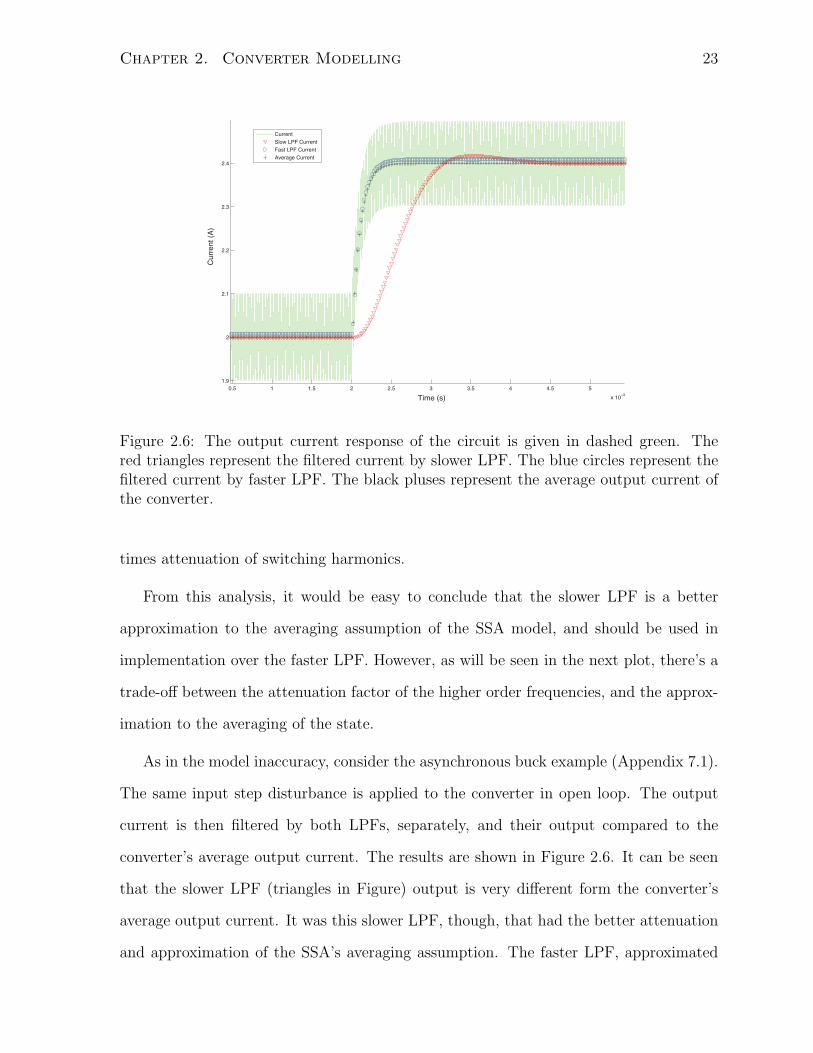
Chapter 2. Converter Modelling 23
0.5 1 1.5 2 2.5 3 3.5 4 4.5 5
x 10−3
1.9
2
2.1
2.2
2.3
2.4
Time (s)
Cu
rre
nt (A
)
Current
Slow LPF Current
Fast LPF Current
Average Current
Figure 2.6: The output current response of the circuit is given in dashed green. Thered triangles represent the filtered current by slower LPF. The blue circles represent thefiltered current by faster LPF. The black pluses represent the average output current ofthe converter.
times attenuation of switching harmonics.
From this analysis, it would be easy to conclude that the slower LPF is a better
approximation to the averaging assumption of the SSA model, and should be used in
implementation over the faster LPF. However, as will be seen in the next plot, there’s a
trade-off between the attenuation factor of the higher order frequencies, and the approx-
imation to the averaging of the state.
As in the model inaccuracy, consider the asynchronous buck example (Appendix 7.1).
The same input step disturbance is applied to the converter in open loop. The output
current is then filtered by both LPFs, separately, and their output compared to the
converter’s average output current. The results are shown in Figure 2.6. It can be seen
that the slower LPF (triangles in Figure) output is very different form the converter’s
average output current. It was this slower LPF, though, that had the better attenuation
and approximation of the SSA’s averaging assumption. The faster LPF, approximated

Chapter 2. Converter Modelling 24
1.6 1.8 2 2.2 2.4 2.6
x 10−3
1.9
2
2.1
2.2
2.3
2.4
2.5
Time (s)
Cu
rre
nt (A
)
Current
Slow LPF Current
Fast LPF Current
Average Current
Figure 2.7: The faster LPF has relatively accurate transient response but also a steadystate error.
the average output current better in the transient region, but has a steady state error
that the slower LPF does not. Figure 2.7 shows the faster LPF response only.
There is an associated trade-off between the steady state and transient accuracy of
the filters, and their approximation to the SWA (i.e. (2.12)). If the filter attenuates
all high frequency terms (i.e. slow filter), then it will approximate (2.12) well in steady
state at the expense of not outputting the average value during transients. Similarly
if the filter is fast, the transient response of its output matches the converter’s average
better, but at the cost of steady state error.
This trade-off in the implementation of the averaging assumption of the SSA model
is a further justification for the derivation of an improved model.
2.4 Summary
In this chapter SSA modelling was analyzed in detail. At its fundamental development,
SSA modelling relies on the assumption of low switching ripple, namely the averaging

Chapter 2. Converter Modelling 25
approximation. The net change in the current or voltage during a single switching period
is unaffected by the switching ripple. This is modelled using the SWA integral, and it
allows for the development of an LTI model representation of the converter. Results
showed that the SSA model has limitations, and conventional implementations of SSA
based controllers introduce further challenging design trade-offs.
Both the modelling and implementation inaccuracies of the SSA model merit the
development of an enhanced modelling approach. The new modelling technique should
not rely on the averaging approximation or any assumptions that lead to the addition
of unmodelled dynamics, like those of the LPF. In addition the new model must have
a better transient and steady error accuracy than SSA. These are the objectives of the
thesis, and the next chapter develops such a model.

Chapter 3
DC/DC Modelling
In the previous chapter the limitations of SSA for modelling converters were outlined.
The aim of the thesis is to present a new modelling approach that does not have such lim-
itations. This chapter focusses on the development of such models for DC/DC converter
application. In DC/DC converters the main control objective is regulation of certain
voltages, currents, or a combination thereof, to a reference value. As such, the new
model needs to represent the actual average of the quantity of interest, while accurately
preserving all system dynamics.
A DC/DC converter transfers power between two voltage levels. This requires regu-
lation of the average of the output current or voltage to track a constant reference value.
A suitable model of the converter is one that represents the averaged output variable
as a state variable. This averaging state needs to take the switching dynamics of the
converter into account. The difference between this approach and the SSA model is that
the dynamics of the averaging process are explicitly modelled and not abstracted away
and neglected, as is the case in the conventional SSA approach. The new model can be
suitably called the Advanced Time Averaging Model (ATAM), as it improves on the SSA
approach by including the averaging dynamics in the state space representation of the
system.
26

Chapter 3. DC/DC Modelling 27
The first step in developing the ATAM, involves the derivation of a generic method for
augmenting linear time varying system equations with an additional state that provides
the integral of any state of the original system. Through a proposed dicretization process,
a new system output may be created that provides the average sliding window average
of the state of interest.
3.1 Sliding Window Average
The sliding window average integrates a signal, which maybe either continuous or discon-
tinuous, between two points in time and precisely computes its average value. Because
the window’s end points can be (together) moved to focus on any portion of a signal,
it is referred to as a ‘sliding’ window average (SWA). This applies to the task at hand,
which is to calculate the average value of a signal during a specified length of time. Of
interest is to augment the linear time varying differential equations with an additional
state (or set of states) that enable output of the SWA of any desired system state (or set
of states). Consider a general LTV system with dynamics:
x(t) = A(t)x(t) (3.1)
where x ∈ Rn, A(t) ∈ nRn; suppose the state of interest is the mth (m ∈ R1, 1 ≤ m ≤ n)
state xm. To compute the SWA of this state, the following equation is employed:
ρ(t) =1
T
∫ t
t−T
xm(τ)dτ (3.2)
The above equation calculates the signal average over the last T seconds. Figure 3.1
shows the SWA. The area under the signal over the last T seconds is integrated and
weighted to produce the average of the signal – ρ(t).
Note that (3.2) is a bounded integral of a state. The goal is to augment the system

Chapter 3. DC/DC Modelling 28
xm(τ)
t− T t τ
ρ(t)
Figure 3.1: The figure shows how the integral in (3.2) calculates SWA.

Chapter 3. DC/DC Modelling 29
of (3.1) with the signal average. (3.2) can be rewritten:
ρ(t) =1
T
∫ t
0
xm(τ)dτ −1
T
∫ t−T
0
xm(τ)dτ (3.3)
Taking the time derivative on both side of the equation:
ρ(t) =1
Txm(t)−
1
Txm(t− T ) (3.4)
The rate of change of the averaging state, ρ(t), is seen to depend on the original state of
interest and a time delayed version of the state. Although the first term of the equation
(3.4) is easy to augment into (3.1), the second term, namely the time delayed term, is not
trivial. This is due to the fact that time delays cannot be precisely modelled by differential
equations of finite order. A further complication that may arise if approximations are
made is that, while the SWA output is bounded, the two integrals of (3.3) represent
unbounded signals.
Fortunately, there’s a way of augmenting SWA dynamics into the system. A new
‘integrating state’ is defined as follows:
xn+1(t) =1
T
∫ t
0
xm(τ)dτ (3.5)
This allows the ρ(t) signal of (3.3) to be expressed as a function that depends exclusively
on the newly defined state:
ρ(t) = xn+1(t)− xn+1(t− T ) (3.6)
Prior to attempting evaluation of (3.7), the augmented system dynamics are defined as:
x(t) = A(t)x(t) (3.7a)

Chapter 3. DC/DC Modelling 30
xn+1(t) =1
Txm(t) (3.7b)
(3.7c)
defining:
xa(t) =
⎡
⎢
⎣
x(t)
xn+1(t)
⎤
⎥
⎦
(3.8)
(3.7) can be expressed as:
xa(t) = A(t)xa(t) (3.9)
The dynamics of the integrating state, xn+1, have thereby been augmented in the con-
tinuous time system, though the SWA value, given by ρ(t), is not yet available.
The form of SWA dynamics in (3.6) suggest that they are more conveniently repre-
sented in discrete time. Assuming a sampling period T , that is equal to the averaging
period yields:
ρ (kT ) = xn+1 (kT )− xn+1 (kT − T ) (3.10)
This represents the SWA dynamics as a discrete time LTI system. Thus it is convenient
for the full system (3.9), to be discretized with period T . The system (3.9) remains a
linear time varying dynamical system. A general solution can be written of the form:
x(t+ T ) = Φ(t, t+ T )x(t) (3.11)
where the subscript a, has been dropped from notation for convenience. The above
equation (3.11), is the solution to (3.1); Φ(t, t + T ) is a state transition map of the
piecewise linear system. Discretizing (3.11) gives:
x (kT + T ) = Φ (kT )x (kT ) (3.12)
Chapter 3. DC/DC Modelling 31
For notational convenience such difference equations will be written in the following form:
x [k + 1] = Φ[k]x [k] (3.13)
And similarly (3.10) will be written in form:
ρ [k] = xn+1 [k]− xn+1 [k − 1] (3.14)
which is the integration of the state over the last switching period. The advantage now, is
that this equation is easily representable in discrete time, though it requires augmentation
of a second ‘delay integrator state’ as follows:
xn+2 [k + 1] = xn+1 [k] (3.15)
The SWA average is then given by:
y [k] =
[
0 0 · · · 0 1 −1
]
x [k] (3.16a)
ρ [k] = y [k] = xn+1 [k]− xn+2 [k] (3.16b)
This quantity will be considered as the system output y [k] for the remainder of this work.
In this section, the system (3.1) was augmented with two additional,integrating and
time-delayed integrating, states for the purpose of producing a single SWA. In addition
both states, as integrating states, are unbounded. A system with unbounded states is
difficult to control, due to the presence of internal state instability. There is a more
elegant solution which only requires one additional state.

Chapter 3. DC/DC Modelling 32
3.1.1 Elimination of the Delayed Integrator State
Elimination of the delayed integrator state requires re-examination of the continuous
time system equation:
xa(t) = A(t)xa(t) (3.17)
Recall the last state is the integrating state as represented by:
xn+1(t) =1
Txm(t) (3.18)
If the system (3.17) is discretized such that:
xa [k + 1] = Φ [k]xa [k] (3.19)
Then the last state, namely the integrating state, will have dynamics given by:
xn+1 [k + 1] =
[
G[k] 1
]
x [k] (3.20a)
G[k] =
[
Φn+1,1 [k] Φn+1,2 [k] · · · Φn+1,n [k]
]
(3.20b)
This may be re-written as:
xn+1 [k + 1] = xn+1 [k] +G[k]
⎡
⎢
⎢
⎢
⎢
⎢
⎢
⎢
⎣
x1[k]
x2[k]
...
xn[k]
⎤
⎥
⎥
⎥
⎥
⎥
⎥
⎥
⎦
(3.21)
Therefore in discrete time, the integrating state is the summation of the previous inte-
grating state’s value, xn+1 [k], and a contribution from the remaining states, scaled by a
vector G. To implement sliding window averaging the previous integrating state’s value

Chapter 3. DC/DC Modelling 33
may simply be discarded by modifying (3.20a):
xn+1 [k + 1] =
[
G[k] 0
]
xa [k] (3.22)
That is the (n+ 1, n+ 1) entry of Φ [k] is modified from unity to zero. The states of the
discrete time system now remain bounded (provided the continuous time system variables
remain bounded).
For each state of interest there is now only the addition of a single state that allows
for SWA. The procedure can be summarized, from the viewpoint of converter systems:
1. Write out the dynamics of the circuit in all possible switching positions, expressing
the system as an autonomous system.
2. Augment these dynamics to include integration states of all the quantities of inter-
est.
3. Write out the evolution of the system over one switching period.
4. Discretize the augmented sytem with switching period T .
5. Modify the integrating states’ dynamics of the linearized system turning them into
SWA values.
3.2 ATAM Application Example
Now that there is a way of augmenting a system with the SWA of any of quantity, the new
modelling approach can be formulated with a general DC/DC converter example. The
converter has different dynamics depending on S(t). The synchronous buck converter
example will be used for development. It is important to note that the method can be
readily applied to any topology. Let x(t), contain the inductor current, and capacitor
voltage, as well as all of the voltage/current inputs. This is done to convert the system

Chapter 3. DC/DC Modelling 34
to an autonomous form, which makes the derivation of the new modelling technique
more convenient. Then in the on, and off position the dynamics can be represented,
respectively:
x(t) =
⎧
⎪
⎨
⎪
⎩
Aonx(t), S(t) = 1
Aoffx(t), S(t) = 0(3.23a)
x(t+ T ) = eAoff (1−d(t))T eAond(t)Tx(t) (3.23b)
where Aon, and Aoff , are ∈ nRn and capture the dynamics of all states in the on and off
switch state respectively; d(t) is the duty cycle of the primary switch. Equation (3.23b)
is the exact evolution of the converter’s dynamics, assuming ideal switches. It is linear
time variant (LTV) system.
Without loss of generality, the output of the system will be the SWA of state x1.
Following with the first step in Section 3.1, both the on and off dynamics are augmented
with a single state:
Aon =
⎡
⎢
⎢
⎢
⎢
⎢
⎢
⎢
⎣
Aon
0
...
0
1 0 · · · 0
⎤
⎥
⎥
⎥
⎥
⎥
⎥
⎥
⎦
(3.24)
Aoff =
⎡
⎢
⎢
⎢
⎢
⎢
⎢
⎢
⎣
Aoff
0
...
0
1 0 · · · 0
⎤
⎥
⎥
⎥
⎥
⎥
⎥
⎥
⎦
(3.25)
A single switching period consists of some interval when the switch is on, followed by
another interval when the switch is off. This progression can be written as:
x[k + 1] = Φ[k]x[
k]
(3.26a)

Chapter 3. DC/DC Modelling 35
Φ[k] = eAoff
(
1−d[k])
T eAond[k]T (3.26b)
where d [k] represents the duty cycle for the kth switching period. The system is linear
time variant (LTV) as Φ depends on d [k].
3.3 Validation
Before linearizing the new model it is worthwhile to test its accuracy. Namely, whether
the augmented state that calculates the SWA, in fact does so with better accuracy than
the SSA model. The same buck example from Appendix 7.1 is used. A step in the duty
cycle is applied at 0.8 ms from 0.5 to 0.6. The converter is simulated in PLECS, and
its output current is averaged using ideal SWA. Similarly the ATAM of the converter is
simulated under the same inputs. Its output state, which should be SWA of the output
curremt, is compared with that of the converter.
Results are showin in Figure 3.2. The ATAM exactly matches the average output
current, in both steady state and transience. Compared to the SSA model in the previous
chapter, which was also simulated under the same conditions, the ATAM is a precise
representation of the discrete time dynamics of the converter. The SSA model is not
accurate due to its assumptions as already discussed.
3.4 Summary
In this chapter a new model approach was developed for modelling DC/DC converters.
This new model is called ATAM. It is based on the exact switching dynamics of the
converter. Through augmentation of a single state a SWA output may be computed. A
buck converter example was used to demonstrate the ATAM procedure. The new model
is LTV. For more common control design applications, it is possible to eliminate the time
variance through a process of linearization. That is the primary objective of the next

Chapter 3. DC/DC Modelling 36
0.8 1 1.2 1.4 1.6 1.8
1.9
2
2.1
2.2
2.3
2.4
Time (ms)
Cur
rent
(A)
CurrentSWA currentATAM output current
Figure 3.2: The open loop response of the current to a duty cycle disturbance. TheATAM precisely predicts the simulated current’s average waveform.

Chapter 3. DC/DC Modelling 37
chapter.
The model presented in this chapter is significant as it is, to date, the first successful
attempt at capturing converter’s output averaging dynamics in a mathematical model.
There are no assumptions made with respect to the harmonic composition of the output,
nor any other limiting assumptions.

Chapter 4
DC/DC Model Linearization and
Control
The newly developed model in the previous chapter augmented a LTV system, with
an additional state representing the dynamics of the SWA of the system output. The
model is an accurate representation of a DC/DC converter; it makes no assumptions, nor
excludes any dynamics. However, as a result of the augmentation technique employed,
the new model is linear time variant (LTV). SSA and other modelling approaches are
commonly used because they represent the system by an LTI model that is valid about the
desired operating point. Many controller design techniques are available for LTI systems
and their implementation is straightforward. This chapter demonstrates that existing
linearization and control techniques may be readily applied to the derived LTV converter
models. This will be demonstrated via control design example for a buck converter. The
LTI model will then be validated. The performance of a controller design based on the
derived LTI model will be compared with that of a controller design based on the SSA
model.
38

Chapter 4. DC/DC Model Linearization and Control 39
4.1 Linearization
LTV systems can be linearized about an operating point, thought the linearization process
is quite distinct from that used for linearization of continuous time nonlinear systems.
Much like the SSA model, linearization is acceptable as a converter is typically operated
around such an operating point. Recall from the last chapter, the synchronous buck
system equations are as follows:
x(t) =
⎧
⎪
⎨
⎪
⎩
Aonx(t), S(t) = 1
Aoffx(t), S(t)=0(4.1a)
Aon =
⎡
⎢
⎢
⎢
⎢
⎢
⎢
⎢
⎣
Aon
0
...
0
1 0 · · · 0
⎤
⎥
⎥
⎥
⎥
⎥
⎥
⎥
⎦
(4.1b)
Aoff =
⎡
⎢
⎢
⎢
⎢
⎢
⎢
⎢
⎣
Aoff
0
...
0
1 0 · · · 0
⎤
⎥
⎥
⎥
⎥
⎥
⎥
⎥
⎦
(4.1c)
x[k] = Φ[
d[k]]
x[
k − 1]
(4.1d)
Φ[k] = eAoff
(
1−d[k])
T eAond[k]T (4.1e)
For clarity in (4.1d) we explicitly show the dependance of Φ on d, where d may vary
with each period. The state that is of interest, namely the output of the system, will be
the first state. Equation (4.1d) and (4.1e) are the new model of the chosen system. To
linearize this model the following notation is introduced:
x [k] = x [k]−Xeq (4.2a)
Chapter 4. DC/DC Model Linearization and Control 40
d [k] = d[k]−Deq (4.2b)
x [k + 1] =∂Φ
∂x
∣
∣
∣
∣
Xeq,Deq
x [k] +∂Φ
∂d
∣
∣
∣
∣
Xeq,Deq
d [k] (4.2c)
∂Φ
∂x
∣
∣
∣
∣
Xeq,Deq
= Φ(Deq) (4.2d)
∂Φ
∂d
∣
∣
∣
∣
Xeq,Deq
=
(
−AoffTeAoff
(
1−Deq
)
T eAonDeqT + eAoff
(
1−Deq
)
T eAonDeqT AonT
)
Xeq
(4.2e)
where the operating point is chosen and represented by the set (Xeq, Deq). The system’s
small signal dynamics are therefore given as follows:
x [k + 1] = Adx [k] +Bdd [k] (4.3a)
Ad =∂Φ
∂x
∣
∣
∣
∣
Xeq,Deq
(4.3b)
Bd =∂Φ
∂d
∣
∣
∣
∣
Xeq,Deq
(4.3c)
y[k] = Cdx[k] =
[
0 · · · 0 1
]
x[k] (4.3d)
Since this is now the linearized state space representation of the circuit, and the integrat-
ing state has been augmented, the remaining two steps of Section 3.1 can be performed.
The SWA state’s dynamics in (4.3a) are modified as to perform SWA. So if:
xn+1 [k + 1] =
[
Ad(n+1,1) Ad(n+1,2) · · · Ad(n+1,n) 1
]
(4.4)
This is replaced by:
xn+1 [k + 1] =
[
Ad(n+1,1) Ad(n+1,2) · · · Ad(n+1,n) 0
]
(4.5)
With the SWA state augmented to the DC/DC system, the new state space representation
encapsulates the dynamics of the circuit linearized around the desired operating point.

Chapter 4. DC/DC Model Linearization and Control 41
This linearized model, can be suitably called Linearized Advanced Time Averaging Model
(LATAM) of the DC/DC system. In terms of output to the system (4.3a), the SWA
output variable is provided as:
y [k] =
[
0 0 · · · 0 1
]
x [k] (4.6)
Again the steps to derive LATAM representation of a general DC/DC topology can be
summarized:
1. Write out the dynamics of the circuit in all possible switching positions, expressing
the system as an autonomous system.
2. Augment these dynamics to include integration states of all the quantities of inter-
est.
3. Write out the evolution of the system over one switching period.
4. Discretize the augmented system with switching period T .
5. Linearize this system around a desired operating point.
6. Modify the integrating states’ dynamics of the linearized system turning them into
SWA values.
Note that the last two steps are interchangeable, the linearization can be done first, or
the discrete model’s dynamics can be modified for the augmented states to make them
memoryless. If linearization is not needed, then that step can be skipped.
While the advantages of this modelling approach will be outlined in greater depth in
the ensuing sections, it can already be seen that this approach offers some benefits. The
first is the fact that this approach does not suffer from aliasing issues. The true average
is calculated through the augmented state (SWA), which rejects high order frequency

Chapter 4. DC/DC Model Linearization and Control 42
components of the state. Second, the model presented is of the form d [k] to y [k]. This
is the output and input of a conventional digital controller for converters.
4.2 Model Demonstration
With the development of the LATAM for DC/DC, its accuracy and performance need to
be tested and compared to SSA. The focus of this section will be on using the LATAM, for
the DC/DC topology, in designing a controller. The performance of this controller will
be compared against that of one designed using SSA model. In addition, the accuracy of
both modelling techniques will be compared in an open loop scenario. The closed-loop
performance determines the degree of improvement over SSA. Since the new modelling
does not suffer from aliasing issues and models all system latencies, a better performance
is expected.
4.2.1 Open Loop Performance
As seen already in previous chapters, one way of validating a model’s accuracy is to check
its open loop response under an input disturbance, and compare it with the converter’s
response. From Chapter 2, it was shown that the ATAM output precisely matched the
simulated converter’s response (sampled). Thus, ATAM will be used as the benchmark,
and representation of the converter’s response. The same asynchronous buck example is
used for this open-loop comparison, as detailed in Appendix 7.1.
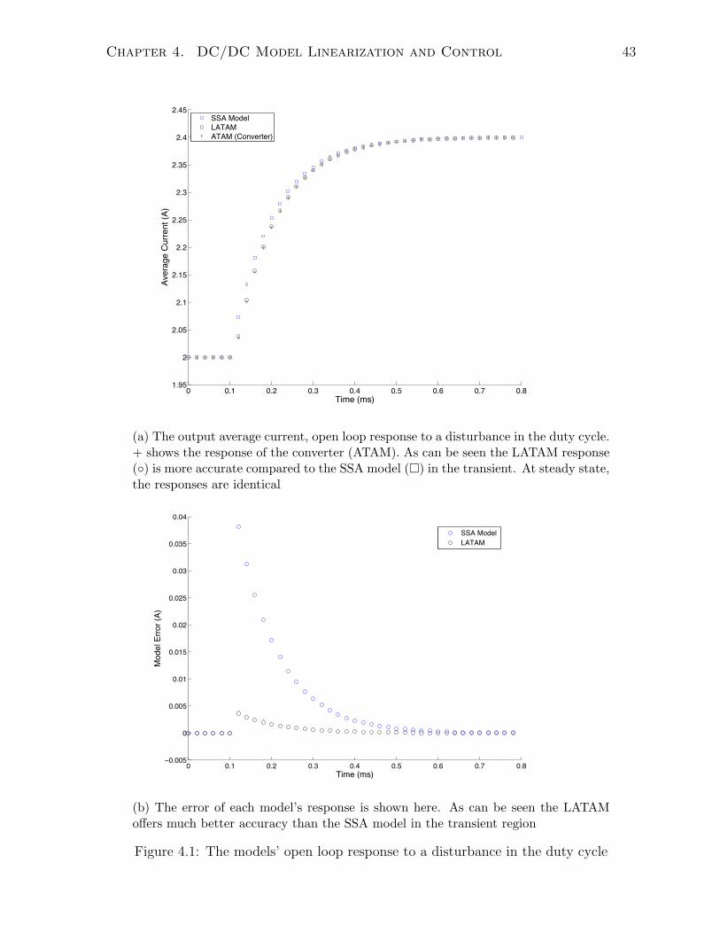
The results are shown in Figure 4.1a. The three model responses are shown: ATAM
(converter), SSA, and the LATAM. At time 2 ms, a disturbance in the duty cycle is
applied. The ATAM output is what the LATAM of the converter, and SSA model aim to
achieve. From the figure it can be seen that LATAM is closer to the actual average output
current during the disturbance. Figure 4.1 shows the models’ error to really differentiate
between the performance accuracy of the two models. This is an encouraging result. It
Chapter 4. DC/DC Model Linearization and Control 43
0 0.1 0.2 0.3 0.4 0.5 0.6 0.7 0.81.95
2
2.05
2.1
2.15
2.2
2.25
2.3
2.35
2.4
2.45
Time (ms)
Aver
age
Cur
rent
(A)
SSA ModelLATAMATAM (Converter)
(a) The output average current, open loop response to a disturbance in the duty cycle.+ shows the response of the converter (ATAM). As can be seen the LATAM response() is more accurate compared to the SSA model (!) in the transient. At steady state,the responses are identical
0 0.1 0.2 0.3 0.4 0.5 0.6 0.7 0.8−0.005
0
0.005
0.01
0.015
0.02
0.025
0.03
0.035
0.04
Time (ms)
Mod
el E
rror (
A)
SSA ModelLATAM
(b) The error of each model’s response is shown here. As can be seen the LATAMoffers much better accuracy than the SSA model in the transient region
Figure 4.1: The models’ open loop response to a disturbance in the duty cycle

Chapter 4. DC/DC Model Linearization and Control 44
+
-
+
-vi(t)
L
vo(t)
io(t)
d(t)
Figure 4.2: The test converter topology. There is no output capacitor – it is extractedout to the output side.
validates the linearization of the ATAM. By doing so the new model is not only more
accurate than the SSA in open-loop but it also models the ‘filtering’ (SWA) of the output
current as a state.
4.2.2 Closed Loop Performance
As seen before, the new DC modelling approach revolves around the linearization of the
ATAM of a DC/DC converter around a chosen operating point. Thus, any inaccuracies in
the modelling will be only because the linear time variant model was linearized. However,
the claim is still that in spite of this linearization, the end result will be a more accurate
model.
For the purpose of comparing the different modelling techniques under closed loop
a modified example has been chosen, and is shown in Figure 4.2. The converter is still
asynchronous buck; the load has been changed to a constant voltage source – or a motor.
Chapter 4. DC/DC Model Linearization and Control 45
The topology (Figure 4.2) has been chosen for several reasons. First, to keep the
modelling simple, the output capacitor has been removed. Having it there only adds
an additional state that has to be modelled. Further, the control objective for this
topology will be maintaining the output current at a certain reference value. This is
equivalent to a constant power exchange with the output, as the output is a motor with
fixed voltage. The load has been changed from resistive to a motor, mainly because the
damping characteristics at a resistor aid to reduce the effect of any imposed disturbances
on the current. The goal is to do a fair comparison between the new model and the SSA,
thus removing unaccounted factors and minimizing variables.
As the control objective is keeping the output current constant reference value, the
disturbance response of the controller will be compared. Specifically load disturbance
(load voltage change), will be applied in order to see how the controller responds.
Model Setup
Before designing the controller, the new model for the presented topology (Figure 2.1)
is derived. The SSA model is needed as well for its own controller design. Detailed
derivation of both methods is presented in Appendix 7.2. Exemplary circuit parameters
are also chosen in Appendix 7.2.
With the two models of the given topology derived, the comparison analysis can be
performed. The main comparison is closed-loop disturbance rejection. Building on the
accuracy of the ATAM, the most important comparison is the use of the new modelling
to design a better controller. As stated the control objective will be to maintain the
output current at a constant reference value. The SSA model will be also used to design
a controller, whose performance will be essentially the benchmark of this test. Next, the
controllers for each model are designed.

Chapter 4. DC/DC Model Linearization and Control 46
+ +
+|
+-
replacemen
0 C(z) Converter
io,avg[k]
PWM
SWAio(t)
io(t)
Io
D
Figure 4.3: The simulation block diagram. The controller acts on the small-signal averageoutput current error, and outputs a small-signal duty cycle. The operating point dutycycle D is added to this before being fed into digital PWM. Digital PWM drives theswitches of the converter.
Controller Design
Digital controllers are commonly used for converter applications. For the given example,
a conventional digital controller will be implemented, and the whole system simulated
in a detailed time domain simulation. The system setup is shown in Figure 4.3. The
controller receives the error in the output current, and outputs the corrective duty cycle.
This duty cycle is processed through a digital PWM, which then converts it into S(t),
the switching state. The switching state signal controls the behaviour of the converter.
The calculate the deviation from the reference output current, the converter’s out-
put current is measured. Depending on whether a SSA, or LATAM controller is being
implemented, a LPF or SWA in hardware, respectively, is implemented in the feedback
as shown on the same figure. SWA in hardware can be accomplished in different ways.
One common method is to oversample the measured output current (many samples in
one switching period), and average the samples for one switching period [4]. This is a
simple, and accurate method that can be easily implemented in a DSP.
The LATAM is a discrete time model of the system. There are many different con-
troller design techniques that can be applied to such model. For simplicity, a root locus
method will be used. In addition, with both models, a Proportional Integrator (PI)

Chapter 4. DC/DC Model Linearization and Control 47
controller will be used for fair comparison. A digital PI controller can be approximated
as:
C(z) = Kp +Ki
z − 1(4.7)
The controller design for the new model is shown in Appendix 7.2.1. The root locus
method for discrete time systems leads to a discrete controller with gains Ki = 0.401
and Kp = 1.889. The control design for the SSA model is shown in Appendix 7.2.2 with
gains Ki = 0.339 and Kp = 1.669.
Notably, the gains of the two controllers are relatively similar. It is the use of the
LPF vs. SWA, that will determine the performance difference between the two models.
Results
The controllers are implemented, and the output current response is recorded for a load
disturbance. The load’s voltage is decreased from 5V to 2V. The average output current
response for both controllers is shown in Figure 4.4.
The results for this disturbance test, show that the LATAM based controller performs
better. The overshoot of the average output current is smaller than the case for the SSA
model based controller. Also, the SSA model based controller results in a steady state
error. The LATAM based controller does not.
The response of the SSA model based controller shows that, the controller is relatively
aggressive. This can be seen in Figure 4.4, at around 2.15 milliseconds; showing as a high
frequency oscillation in the response. Such oscillations are a sign of a controller that is
as fast as can be without pushing the system into instability. The steady state error,
as discussed before, is due to the optimization between fast LPF and transient response
and steady state inaccuracy. The new model has no such trade-offs.
The fact that the SSA model based controller is designed under aggressive criteria,
and still is outperformed by the LATAM based controller also shows the advantage of
using LATAM and SWA over SSA and LPF.

Chapter 4. DC/DC Model Linearization and Control 48
SSA
LATAM
Figure 4.4: The average output current response for a load decrease disturbance. TheSSA model based controller has higher overshoot and steady state error; LATAM basedcontroller has smaller overshoot and no steady state error.

Chapter 4. DC/DC Model Linearization and Control 49
4.3 Summary
In this chapter the new model, ATAM, was linearized and used for control design. It was
shown that the controller performance based on the LATAM performed better than that
of the SSA model. The open-loop comparison indicated that the LATAM more closely
outputs the average value of its output than the SSA model.
More importantly a closed loop test was carried out. A controller designed using
LATAM was tested under different load disturbances. A second controller designed using
SSA modelling was also tested under the same load disturbances. The LATAM controller
perfumed better – with smaller overshoot and without any steady state error.
Further to this, the presented modelling approach, based on its construct does not
suffer from aliasing. It also captures the complete dynamics of average output controlled
converters. Because SWA is used, there’s no implementation calibration in the same way
LPF needs calibration depending on the different switching frequencies.
Chapter 5
DC/AC Modelling
In Chapter 3 an Advanced Time Averaging Model was developed for DC/DC convert-
ers. DC/AC converters are another widely used type of converter. They are used for
interfacing renewable sources such as solar and wind, to the utility and as back to back
converters for changing the frequency of the AC.
The focus of this chapter will be on developing a new modelling approach for DC/AC
converters. In DC/AC converters, the main control objective is controlling the AC side
current or voltage to a certain reference fundamental sinusoidal value. Comparing to the
DC/DC, the controller needs to track a sinusoidal reference as opposed to constant. First,
however, a mathematical model is needed for calculating AC current/voltage injected by
the converter. This corresponds to calculating the fundamental (frequency of the AC side)
component of that signal, through Fourier Decomposition. The new model needs to be
able to model the incremental contribution to the fundamental component of that signal
during each switching period or subcycle. Past work [11, 12, 25] has focused on deriving
a full DC/AC model including all harmonics by augmenting the Fourier decomposition
integrals. This research will be leveraged in developing the new model.
As will be seen, the new modelling approach leads to a non-LTI model because of the
calculation of the fundamental. Designing a controller from the new model is non-trivial
50
Chapter 5. DC/AC Modelling 51
and does not allow for the use of simple LTI control design techniques. Thus, design of a
DC/AC converter controller is considered outside the scope of this thesis. However, the
accuracy of the new modelling approach is verified. The accuracy of the calculation of
the fundamental contribution during each switching period is checked. For that purpose,
two examples will be used in validating the new model’s accuracy.
5.1 Modelling Challenges
The objective of the chapter is to develop a modelling approach that does not suffer
from aliasing issues and allows for more accurate controller design. DC/AC converters
exchange power between DC and AC. As most inverters are grid tied (AC side), to
accomplish the desired power exchange, the converter needs to be controlled in order
to appropriately shape its AC side current. The reference signal for the controller is
sinusoidally changing - whereas the DC/DC controller tracked a constant reference signal.
The main control objective in the DC domain was to ensure that certain current/voltage
average values follows a reference value. Analogous to this in DC/AC converters, is to
ensure that the converter’s AC current fundamental component follows a certain refer-
ence. Shaping the AC current really refers to ensuring the converter injects current with
the correct amount of fundamental frequency. Determining the magnitude and phase
of the fundamental component of the AC current (or voltage) in a converter topology
is a challenge. Switching frequency is larger than the grid frequency. To calculate the
fundamental component of any signal:
X1(t) =1
Tac
∫ t
t−Tac
x(τ)e−jwoτdτ (5.1)
where Tac is the period of the fundamental frequency, which is much longer than the
switching period; wo is the fundamental frequency in rad/s. To calculate the total fun-
damental component of the signal, a whole fundamental period is needed. This is a

Chapter 5. DC/AC Modelling 52
challenge in AC modelling, as the control decisions must happen at the switching fre-
quency. The new model therefore employs a method for calculating the ‘fundamental
component contribution’ of a signal during a subcycle of the fundamental period.
5.2 Subcycle Fundamental Contribution
To create a new modelling approach, like in the DC/DC case, the first challenge is
developing a way of calculating the fundamental contribution of a signal over a single
switching period. To illustrate, consider the space vector associated with a balanced ac
quantity. In the αβ frame the space vector may be expressed as: x(t) = cos(wot) +
jsin(wot). Per (5.1):
X1(t) =1
Tac
∫ t
t−Tac
(cos(wot) + jsin(wot)) e−jwoτdτ (5.2)
The integral inside simplifies to a constant value of unity, as the multiplication of positive
and negative rotating signals is constant. This integral can be split into subintervals
(subcycles) of switching period, T :
X1(t) =1
Tac
∫ t
t−T
1dτ +1
Tac
∫ t−T
t−2T
1dτ + · · ·+1
Tac
∫ t−(mf−1)T
t−mfT
1dτ (5.3)
For a perfect oscillator, the subcycles have equal contribution to the fundamental fre-
quency (Figure 5.1)
Thus evaluating (5.1) for a subcycle time, gives the subcycle fundamental contribution
(SFC), represented as X1sw(t).
X1sw(t) =
1
Tac
∫ t
t−T
x(τ)e−jwoτdτ (5.4)
where X1sw(t) = X1
sw,re(t) + jX1sw,im(t) This integral, will need to be augmented into the

Chapter 5. DC/AC Modelling 53
T Tac t
X1(t)
Figure 5.1: The integrator in (5.3) leads to equal sub-integrals which form a straight linefor a perfect oscillator
system so that the SFC of the signal of interest is available as a state at the end of each
switching period. Fortunately, equation (5.4) is of a special form [8]. First, consider a
general differential equation of the form:
dy
dt(t) = m · y(t) + h · q(t) (5.5)
the general solution to this is:
y(t) = emty(t− to) +
∫ t
t−to
em(t−τ)h · q(τ)dτ (5.6)
The above equation describes the integral that calculates SFC with the following substi-
tutions:
y(t− to) = 0 (5.7a)
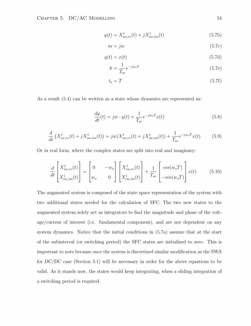
Chapter 5. DC/AC Modelling 54
y(t) = X1sw,re(t) + jX1
sw,im(t) (5.7b)
m = jw (5.7c)
q(t) = x(t) (5.7d)
h =1
Tac
e−jwoT (5.7e)
to = T (5.7f)
As a result (5.4) can be written as a state whose dynamics are represented as:
dy
dt(t) = jw · y(t) +
1
Tac
e−jwoTx(t) (5.8)
d
dt
(
X1sw,re(t) + jX1
sw,im(t))
= jw(X1sw,re(t) + jX1
sw,im(t)) +1
Tac
e−jwoTx(t) (5.9)
Or in real form, where the complex states are split into real and imaginary:
d
dt
⎡
⎢
⎣
X1sw,re(t)
X1sw,im(t)
⎤
⎥
⎦
=
⎡
⎢
⎣
0 −wo
wo 0
⎤
⎥
⎦
⎡
⎢
⎣
X1sw,re(t)
X1sw,im(t)
⎤
⎥
⎦
+1
Tac
⎡
⎢
⎣
cos(woT )
−sin(woT )
⎤
⎥
⎦
x(t) (5.10)
The augmented system is composed of the state space representation of the system with
two additional states needed for the calculation of SFC. The two new states to the
augmented system solely act as integrators to find the magnitude and phase of the volt-
age/current of interest (i.e. fundamental component), and are not dependent on any
system dynamics. Notice that the initial conditions in (5.7a) assume that at the start
of the subinterval (or switching period) the SFC states are initialized to zero. This is
important to note because once the system is discretized similar modification as the SWA
for DC/DC case (Section 3.1) will be necessary in order for the above equations to be
valid. As it stands now, the states would keep integrating, when a sliding integration of
a switching period is required.

Chapter 5. DC/AC Modelling 55
5.2.1 Modifying SFC States to Memoryless
Before doing a specific DC/AC converter example, the issue regarding the reset of the
SFC states needs to be addressed. Similar to the DC/DC case for SWA the dynamics of
SFC in continuous time integrate and calculate the cumulative fundamental contribution.
The dynamics will need to be modified once the system is discretized so that SFC states
only calculate the current switching period’s fundamental contribution. Similarly to SWA
it will need to become a memoryless state. In order to see the steps needed, a sinusoidal
signal will be considered for which the fundamental component is the only one present.
Let:
x1(t) = cos(wot) (5.11)
x2(t) = sin(wot) (5.12)
Here a second state is needed x2(t), in order to write the dynamics of the sinusoidal
signal. The goal is to calculate the fundamental contribution of each subcycle of the
sinusoid (x1(t)). Two additional states are introduced for SFC calculation:
x3(t) + jx4(t) =1
Tac
∫ t
t−T
x1(τ)e−jwoτdτ (5.13)
In state space form this can be written as per (5.10):
d
dt
⎡
⎢
⎣
x3(t)
x4(t)
⎤
⎥
⎦
=
⎡
⎢
⎣
0 −wo
wo 0
⎤
⎥
⎦
⎡
⎢
⎣
x3(t)
x4(t)
⎤
⎥
⎦
+1
Tac
⎡
⎢
⎣
cos(woT )
−sin(woT )
⎤
⎥
⎦
x1(t) (5.14)
Finally the whole system:
d
dtx(t) = Ax(t) (5.15a)

Chapter 5. DC/AC Modelling 56
A =
⎡
⎢
⎢
⎢
⎢
⎢
⎢
⎢
⎣
0 −wo 0 0
wo 0 0 0
1Tac
cos(woT ) 0 0 −wo
− 1Tac
sin(woT ) 0 wo 0
⎤
⎥
⎥
⎥
⎥
⎥
⎥
⎥
⎦
(5.15b)
As in DC/DC, and as will be seen for the DC/AC case, the value of interest is at the end of
the switching period – since it’s then when control action can take place. Mathematically
this is equivalent to discretizing the system in (5.15a)-(5.15b):
Φ = eAT (5.16a)
x [k + 1] = Φx [k] (5.16b)
where x [k] = x(kT ) The structure of the Φ matrix is as follows:
Φ =
⎡
⎢
⎣
R 0
M R
⎤
⎥
⎦
(5.17)
where:
R =
⎡
⎢
⎣
cos(woT ) sin(woT )
−sin(woT ) cos(woT )
⎤
⎥
⎦
(5.18)
and M ∈ 2R2 is the Fundamental Contribution Matrix (FCM). It relates the states of
the original system to the SFC states - in other words how much each one contributes to
the calculation of the fundamental. The discrete dynamics of the SFC states are:
⎡
⎢
⎣
x3 [k + 1]
x4 [k + 1]
⎤
⎥
⎦
= M
⎡
⎢
⎣
x1 [k]
x2 [k]
⎤
⎥
⎦
+R
⎡
⎢
⎣
x3 [k]
x4 [k]
⎤
⎥
⎦
(5.19)
The SFC states can be considered the coordinates of a vector; Cumulative Fundamental
Contribution (CFC) vector, Hk, on a 2-d plane. The subscript indicates the switching

Chapter 5. DC/AC Modelling 57
period during which the SFC states (vector coordinates) are computed. The position of
the CFC vector is the contribution from the states of interest (Fk) and a rotated version
of the previous position of the CFC vector (Hk−1). Let Fk represent the fundamental
contribution vector (SFC vector) during the kth switching period:
Fk = M
⎡
⎢
⎣
x1 [k − 1]
x2 [k − 1]
⎤
⎥
⎦
(5.20)
Then Hk, which is represented by the SFC states, can be written as:
Hk = M
⎡
⎢
⎣
x1 [k − 1]
x2 [k − 1]
⎤
⎥
⎦
+RFk−1 +R2Fk−2 + · · ·+Rk−1F1 (5.21a)
Hk = Fk +RHk−1 (5.21b)
Since the goal is to only have the fundamental contribution during the current switching
period, the dynamics have to be modified as to eliminate the addition of the previous
vectors. In addition, though, the current contribution from the states of interest need
to be unrotated by the number of switching periods that have already passed. This is
because, unlike the DC averaging case, the frame of reference for each SFC is rotating
by R. This is evident in the dynamics of (5.21a) that the previous vectors are added to
the present vector only after a corrective rotation is applied; thus bringing all vectors in
the same frame of reference. Figure 5.2 shows this graphically for an arbitrary example.
By looking at (5.20) and applying the inverse of the rotation, the following equation is
derived:
Fk,stat = R−(k−1)M
⎡
⎢
⎣
x1 [k − 1]
x2 [k − 1]
⎤
⎥
⎦
(5.22)
Fk,stat represents the SFC during the current subinterval. By multiplying (5.20) by k
inverse rotations, the SFC is brought to the frame of reference at time k = 1. In other

Chapter 5. DC/AC Modelling 58
RH1
H1
H2
F2
β
β
β
β
α
α α
α
Figure 5.2: Shown here is how the SFC vector is calculated for the second switchingperiod. The SFC of the previous switching event is rotated and added to the fundamentalcontribution vector of the second period. Tac
T= 4
words, SFC states are reset every switching period. Further because the SFC is really
the desired output value, the final augmented system is described as:
x [k] =
⎡
⎢
⎣
x1 [k]
x2 [k]
⎤
⎥
⎦
(5.23a)
Φ = R (5.23b)
x [k + 1] = Φx [k] (5.23c)
y [k] = Γx [k] (5.23d)
Γ = R−(k−1)M (5.23e)
(5.23f)
These equations describe the modified discrete system dynamics for the calculation of
the SFC of the states of interest – the perfect oscillator. Thus at any switching period,

Chapter 5. DC/AC Modelling 59
+
-
+
-
~
~
VDC
2
VDC
2
L
LSα(t)
Sα(t)
Sβ(t)
Sβ(t)
iα(t)
iβ(t)
vα(t)
vβ(t)
n
Figure 5.3: The neutral clamped two phase inverter topology is shown here.
k, the fundamental complex Fourier coefficient, during that interval, can be extracted by
the following equation:
C1 [k] = y1 [k] + jy2 [k] (5.24)
With this example, the necessary steps were made that augmented and modified the
original system as to be able to calculate the SFC. The SFC is a combination of two states
in the modified system. The fact the states are ‘reset’ each switching period, satisfies the
condition under which (5.7) was applied. This approach does not rely on averaging of the
states of the system, or waiting a whole line period before calculating the fundamental
component of a state.
5.3 Two Phase Inverter Modelling
For the full development of the new ATAM modelling, a two phase inverter has been
chosen as shown in Figure 5.3. A two-phase inverter is analyzed, as opposed to a three-
phase inverter, for two reasons. First, the two phases are orthogonal, meaning each
phase represents the α and β axis respectively. This, as will be seen later, simplifies

Chapter 5. DC/AC Modelling 60
the construction of the system model (and matrices) as there is no coupling between the
states on different axis. Second, the switching events between phases are uncoupled –
a switching sequence in phase a, does not affect the current in phase b and vice versa.
Suppose, as per Figure 5.3:
vo(t) = vα(t) + jvβ(t) (5.25a)
io(t) = iα(t) + jiβ(t) (5.25b)
Assuming the AC side voltage is ideal, its dynamics can be written as:
d
dt
⎡
⎢
⎣
vα
vβ
⎤
⎥
⎦
=
⎡
⎢
⎣
0 −wo
wo 0
⎤
⎥
⎦
⎡
⎢
⎣
vα
vβ
⎤
⎥
⎦
(5.26)
The objective in the new modelling approach is to augment the system with states that
contain the SFC of the output current io(t). One of the challenges with this is that the
dynamics of io(t) depend on the switching events in phase a, and phase b. This means that
depending on the the switching events for both phases, up to six subintervals, varying in
length, are created so that the evolution of the output current can be computed. Figure
5.4 shows this with an arbitrary example of switching times.
The presence of variably long subintervals creates additional computation that’s com-
plex to model, as the length of different switch positions, changes between each switching
period. It’s not as simple as DC/DC, where the sequence is always the same (on-off-on...).
5.3.1 Decoupled Fourier Transform
The output current can be decoupled into its α, and β phase. For each of its component
currents, the switching order closely resembles the DC/DC case. In fact it is precisely the
same. As such, decoupling the output current into its phase components helps in keeping
the model and calculations relatively simple. The same motivation exists to decouple the

Chapter 5. DC/AC Modelling 61
1 2 3 4 5
Sα(t)
Sβ(t)
t
kT
kT
kT
D1,α [k] D2,α [k] D3,α [k]
D1,β [k] D2,β [k] D3,β [k]
(k − 1)T
Figure 5.4: Shown here is how the different switching times in both phases can lead tomany different circuit states.
SFC calculation of the output current. As in Section 5.2:
I1α + jI1β =1
Tac
∫ t
t−Tac
iα + jiβ(τ)e−jwoτdτ (5.27)
This equation forces the dynamics of the α and β components to be coupled together
in order to calculate the SFC of the output current. Since the goal is to decouple this
calculation as well, (5.27) is re-written into two equations splitting it into the two phase
currents:
I1α,re + jI1α,im =1
Tac
∫ t
t−Tac
iα(τ)e−jwoτdτ (5.28a)
I1β,re + jI1β,im =1
Tac
∫ t
t−Tac
iβ(τ)e−jwoτdτ (5.28b)

Chapter 5. DC/AC Modelling 62
where the equations calculate the SFC of the output current through its phase α, and β
respectively. Solving for them separately, as was done for a general signal in Section 5.2,
their solution can be written:
d
dt
(
I1α,re(t) + jI1α,im(t))
= jw(I1α,re(t) + jI1α,im(t)) +1
Tac
e−jwoT iα(t) (5.29a)
d
dt
(
I1β,re(t) + jI1β,im(t))
= jw(I1β,re(t) + jI1β,im(t)) +1
Tac
e−jwoT iβ(t) (5.29b)
Following the development of Section 5.2.1 and the example of the perfect oscillator, both
systems (α, and β dynamics) can be re-written so that the fundamental contribution for
each system is:
C1α [k] = yα,1 [k] + jyα,2 [k] (5.30a)
C1β [k] = yβ,1 [k] + jyβ,2 [k] (5.30b)
where the notation is consistent with Section 5.2.1 – yα refers to the output vector of
the modified discrete system of the α-frame, xα refers to the state vector of the modified
discrete system of the α-frame. The same notation applies for the β-frame. The SFC of
both frames as per above equations, can be combined together so that the fundamental
contribution (SFC) of the whole system for the state of interest is calculated; that is the
solution to (5.27). This can be easily done. As shown in Figure 5.5, β-frame lags the
α-frame by π2 . Since the SFC coefficients in (5.30a) and (5.30b) are independent, the
total system’s SFC coefficient is as follows:
C1tot [k] = C1
α [k] + jC1β [k] (5.31)
With the decoupling of the SFC calculation, the two-phase inverter example can now
be fully developed. Following the circuit in Figure 5.3 the dynamics for the on and off
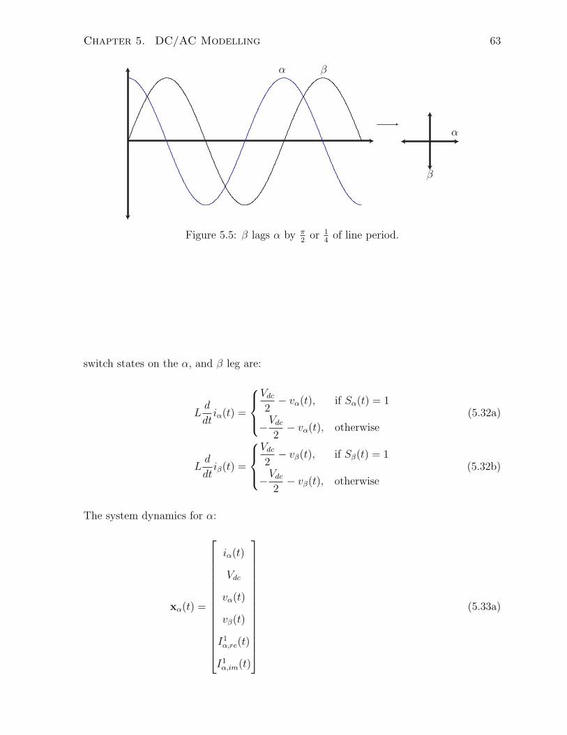
Chapter 5. DC/AC Modelling 63
α
α
β
β
Figure 5.5: β lags α by π2 or 1
4 of line period.
switch states on the α, and β leg are:
Ld
dtiα(t) =
⎧
⎪
⎨
⎪
⎩
Vdc
2− vα(t), if Sα(t) = 1
−Vdc
2− vα(t), otherwise
(5.32a)
Ld
dtiβ(t) =
⎧
⎪
⎨
⎪
⎩
Vdc
2− vβ(t), if Sβ(t) = 1
−Vdc
2− vβ(t), otherwise
(5.32b)
The system dynamics for α:
xα(t) =
⎡
⎢
⎢
⎢
⎢
⎢
⎢
⎢
⎢
⎢
⎢
⎢
⎢
⎢
⎢
⎣
iα(t)
Vdc
vα(t)
vβ(t)
I1α,re(t)
I1α,im(t)
⎤
⎥
⎥
⎥
⎥
⎥
⎥
⎥
⎥
⎥
⎥
⎥
⎥
⎥
⎥
⎦
(5.33a)

Chapter 5. DC/AC Modelling 64
Aα,on =
⎡
⎢
⎢
⎢
⎢
⎢
⎢
⎢
⎢
⎢
⎢
⎢
⎢
⎢
⎢
⎣
0 12L − 1
L0 0 0
0 0 0 0 0 0
0 0 0 −wo 0 0
0 0 wo 0 0 0
1Tac
cos(woT ) 0 0 0 0 −wo
− 1Tac
sin(woT ) 0 0 0 wo 0
⎤
⎥
⎥
⎥
⎥
⎥
⎥
⎥
⎥
⎥
⎥
⎥
⎥
⎥
⎥
⎦
(5.33b)
Aα,off =
⎡
⎢
⎢
⎢
⎢
⎢
⎢
⎢
⎢
⎢
⎢
⎢
⎢
⎢
⎢
⎣
0 − 12L − 1
L0 0 0
0 0 0 0 0 0
0 0 0 −wo 0 0
0 0 wo 0 0 0
1Tac
cos(woT ) 0 0 0 0 −wo
− 1Tac
sin(woT ) 0 0 0 wo 0
⎤
⎥
⎥
⎥
⎥
⎥
⎥
⎥
⎥
⎥
⎥
⎥
⎥
⎥
⎥
⎦
(5.33c)
d
dtxα(t) =
⎧
⎪
⎨
⎪
⎩
Aα,onxα(t), if cα(t) = 1
Aα,offxα(t), otherwise(5.33d)
Similarly for β:
xβ(t) =
⎡
⎢
⎢
⎢
⎢
⎢
⎢
⎢
⎢
⎢
⎢
⎢
⎢
⎢
⎢
⎣
iβ(t)
Vdc
vα(t)
vβ(t)
I1β,re(t)
I1β,im(t)
⎤
⎥
⎥
⎥
⎥
⎥
⎥
⎥
⎥
⎥
⎥
⎥
⎥
⎥
⎥
⎦
(5.34a)
Chapter 5. DC/AC Modelling 65
Aβ,on =
⎡
⎢
⎢
⎢
⎢
⎢
⎢
⎢
⎢
⎢
⎢
⎢
⎢
⎢
⎢
⎣
0 12L 0 − 1
L0 0
0 0 0 0 0 0
0 0 0 −wo 0 0
0 0 wo 0 0 0
1Tac
cos(woT ) 0 0 0 0 −wo
− 1Tac
sin(woT ) 0 0 0 wo 0
⎤
⎥
⎥
⎥
⎥
⎥
⎥
⎥
⎥
⎥
⎥
⎥
⎥
⎥
⎥
⎦
(5.34b)
Aβ,off =
⎡
⎢
⎢
⎢
⎢
⎢
⎢
⎢
⎢
⎢
⎢
⎢
⎢
⎢
⎢
⎣
0 − 12L 0 − 1
L0 0
0 0 0 0 0 0
0 0 0 −wo 0 0
0 0 wo 0 0 0
1Tac
cos(woT ) 0 0 0 0 −wo
− 1Tac
sin(woT ) 0 0 0 wo 0
⎤
⎥
⎥
⎥
⎥
⎥
⎥
⎥
⎥
⎥
⎥
⎥
⎥
⎥
⎥
⎦
(5.34c)
d
dtxβ(t) =
⎧
⎪
⎨
⎪
⎩
Aβ,onxβ(t), if cβ(t) = 1
Aβ,offxβ(t), otherwise(5.34d)
Assuming SPWM for the duty cycle, during a single switching period, there will be three
distinct subintervals, where the primary switches are on-off-on. Figure 5.6 shows the
reason behind this.
Following the above notation, after a single switching period the evolution of the state
vector can be written as:
xα
(
(k + 1)T)
= eAon,αD3,α[k]T eAoff ,αD2,α[k]T eAon,αD1,α[k]Txα(kT ) (5.35)
where D1,α [k] represents the first ‘on’ part of the kth switching period; D2,α[k] represents
the ‘off’ duration of the switch during the kth switching period. Sampling this, with

Chapter 5. DC/AC Modelling 66
34
1
−1
TacTac
2
T
t
t
vref (t)vcar(t)
D1,α [1] D2,α [1]
D3,α [1] D1,α [2]
D2,α [2] D3,α [2]
Figure 5.6: Figure shows how the duty cycle is calculated for SPWM for α subsystem.Here mf = 2 (Tac
T) for visualization purposes. For each switching period there is on-off-on
period.

Chapter 5. DC/AC Modelling 67
period T , results in:
Φα [k] = eAon,αD3,α[k]T eAoff ,αD2,α[k]T eAon,αD1,α[k]T (5.36a)
xα [k + 1] = Φα [k]xα [k] (5.36b)
For this system, Φα changes between switching periods, whereas for the perfect oscillator
example in Section 5.2.1 it didn’t. As a result the FCM is a function of the switching
period.
Φα [k] =
⎡
⎢
⎣
Dα [k] 0
Mα [k] R
⎤
⎥
⎦
(5.37)
such that, the new modified discrete system can be written as:
xα [k] =
⎡
⎢
⎢
⎢
⎢
⎢
⎢
⎢
⎣
xα,1(kT )
xα,2(kT )
xα,3(kT )
xα,4(kT )
⎤
⎥
⎥
⎥
⎥
⎥
⎥
⎥
⎦
(5.38a)
Φα [k] = Dα [k] (5.38b)
xα [k + 1] = Φαxα [k] (5.38c)
yα [k] = Γα [k] xα [k] (5.38d)
Γα [k] = Rk−1Mα [k] (5.38e)
The above equations (5.38a)–(5.38e) describe the full system dynamics of phase α of the
converter as well as the SFC states needed to calculate the coefficient of the fundamental
Fourier transform of the α output current (iα). The above steps follow for phase β. The
equations are identical as (5.38a)–(5.38e), with the respective β matrices, and switching
times. Finally the SFC for the total output current io at the end of each switching period
Chapter 5. DC/AC Modelling 68
is available:
C1α [k] = yα [k] (5.39a)
C1β [k] = yβ [k] (5.39b)
I1o [k] = I1α [k] + jI1β [k] = C1α [k] + jC1
β [k] (5.39c)
This two-phase inverter example has helped in establishing the procedure for calculating
the SFC of the output current, but it can be modified for any current/voltage of interest.
To put this whole procedure in perspective, a flowchart of it is shown (Figure 5.7).
Although the two-phase inverter is a subset of inverter topologies, it helps in demon-
strating the new modelling approach of inverters. There are no assumptions with respect
to the development of the modelling that limit it to two-phase topologies and the pro-
posed methodology in fact can be applied to any dc/ac converter with any number of
phases.
5.4 Model Demonstration
In this section the new AC modelling approach is demonstrated. Instead of taking an
inverter topology, the system under consideration will be an ideal oscillator. The signal
is 100% fundamental component – it has no harmonics. The Fourier transform of an
ideal oscillator is easy to calculate and use as validation for the results given by the new
model.

Chapter 5. DC/AC Modelling 69
Circuit Dynamics
Split into α, β subsystems
Get switchingtimes for α
Get switchingtimes for β
Augment with SFCstate for I1α
Augment with SFCstate for I1β
Get Φα [k]M [k] , yα [k]
I1o [k] = yα [k] + yβ [k]Get Φβ [k]M [k] yβ [k]
∀k∀k
Figure 5.7: Flow chart of the new modelling approach for DC/AC inverter
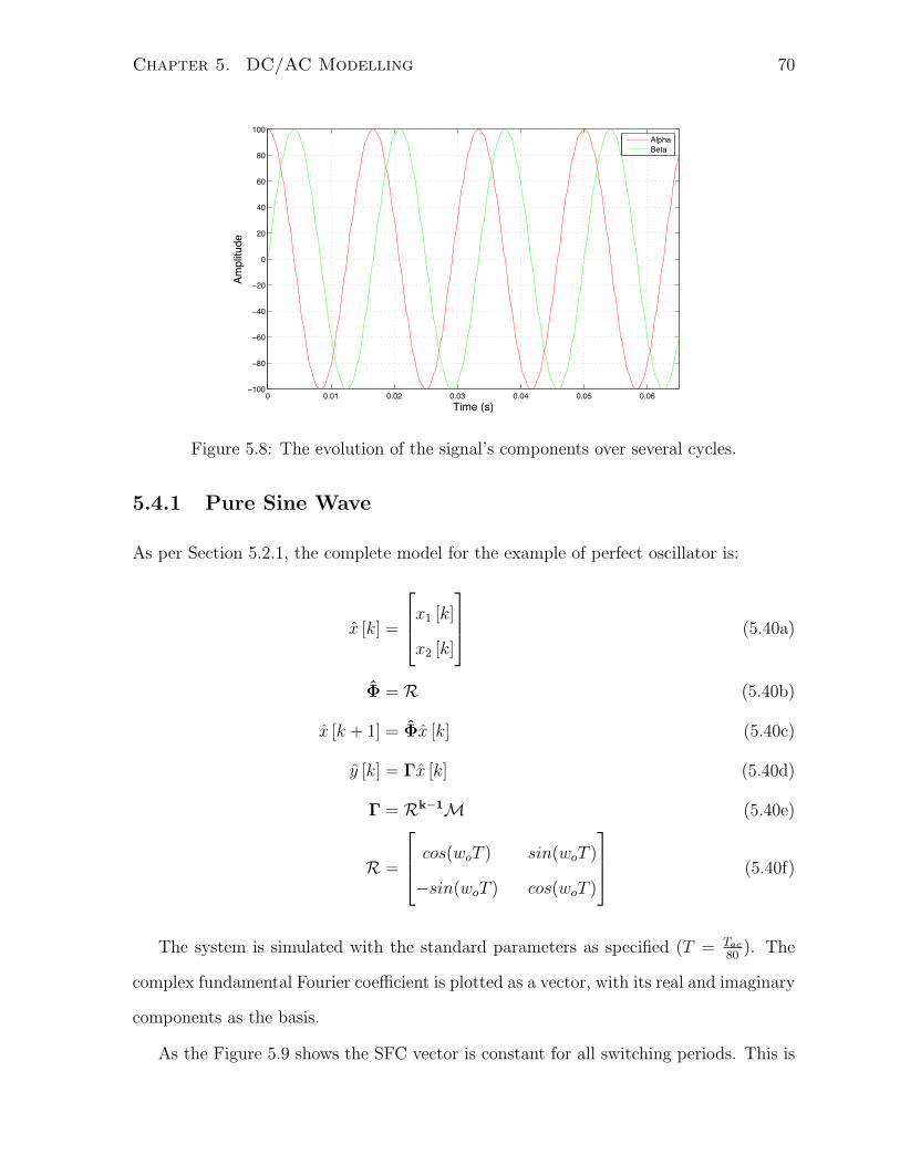
Chapter 5. DC/AC Modelling 70
0 0.01 0.02 0.03 0.04 0.05 0.06−100
−80
−60
−40
−20
0
20
40
60
80
100
Time (s)
Ampl
itude
AlphaBeta
Figure 5.8: The evolution of the signal’s components over several cycles.
5.4.1 Pure Sine Wave
As per Section 5.2.1, the complete model for the example of perfect oscillator is:
x [k] =
⎡
⎢
⎣
x1 [k]
x2 [k]
⎤
⎥
⎦
(5.40a)
Φ = R (5.40b)
x [k + 1] = Φx [k] (5.40c)
y [k] = Γx [k] (5.40d)
Γ = Rk−1M (5.40e)
R =
⎡
⎢
⎣
cos(woT ) sin(woT )
−sin(woT ) cos(woT )
⎤
⎥
⎦
(5.40f)
The system is simulated with the standard parameters as specified (T = Tac
80 ). The
complex fundamental Fourier coefficient is plotted as a vector, with its real and imaginary
components as the basis.
As the Figure 5.9 shows the SFC vector is constant for all switching periods. This is

Chapter 5. DC/AC Modelling 71
0.0125 0.0125 0.0125 0.0125 0.0125
−1
−0.8
−0.6
−0.4
−0.2
0
0.2
0.4
0.6
0.8
1
x 10−12
Re
Im
Figure 5.9: The SFC of the perfect oscillator is constant in all subintervals as representedby the constant point in this plot.
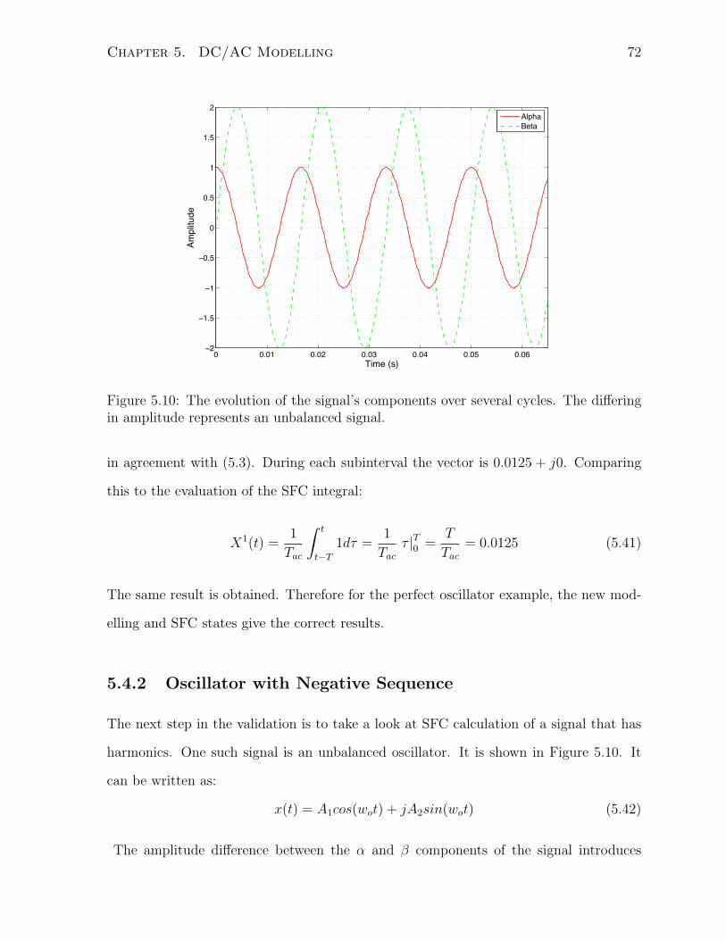
Chapter 5. DC/AC Modelling 72
0 0.01 0.02 0.03 0.04 0.05 0.06−2
−1.5
−1
−0.5
0
0.5
1
1.5
2
Time (s)
Ampl
itude
AlphaBeta
Figure 5.10: The evolution of the signal’s components over several cycles. The differingin amplitude represents an unbalanced signal.
in agreement with (5.3). During each subinterval the vector is 0.0125 + j0. Comparing
this to the evaluation of the SFC integral:
X1(t) =1
Tac
∫ t
t−T
1dτ =1
Tac
τ |T0 =T
Tac
= 0.0125 (5.41)
The same result is obtained. Therefore for the perfect oscillator example, the new mod-
elling and SFC states give the correct results.
5.4.2 Oscillator with Negative Sequence
The next step in the validation is to take a look at SFC calculation of a signal that has
harmonics. One such signal is an unbalanced oscillator. It is shown in Figure 5.10. It
can be written as:
x(t) = A1cos(wot) + jA2sin(wot) (5.42)
The amplitude difference between the α and β components of the signal introduces
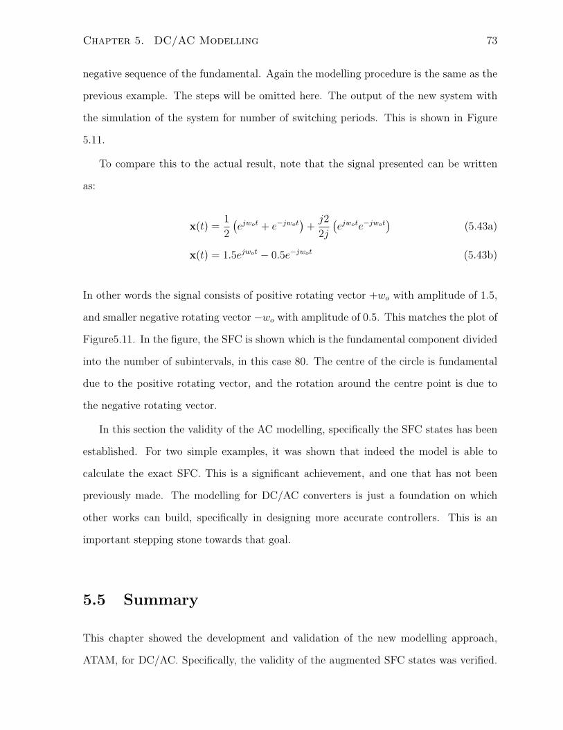
Chapter 5. DC/AC Modelling 73
negative sequence of the fundamental. Again the modelling procedure is the same as the
previous example. The steps will be omitted here. The output of the new system with
the simulation of the system for number of switching periods. This is shown in Figure
5.11.
To compare this to the actual result, note that the signal presented can be written
as:
x(t) =1
2
(
ejwot + e−jwot)
+j2
2j
(
ejwote−jwot)
(5.43a)
x(t) = 1.5ejwot − 0.5e−jwot (5.43b)
In other words the signal consists of positive rotating vector +wo with amplitude of 1.5,
and smaller negative rotating vector −wo with amplitude of 0.5. This matches the plot of
Figure5.11. In the figure, the SFC is shown which is the fundamental component divided
into the number of subintervals, in this case 80. The centre of the circle is fundamental
due to the positive rotating vector, and the rotation around the centre point is due to
the negative rotating vector.
In this section the validity of the AC modelling, specifically the SFC states has been
established. For two simple examples, it was shown that indeed the model is able to
calculate the exact SFC. This is a significant achievement, and one that has not been
previously made. The modelling for DC/AC converters is just a foundation on which
other works can build, specifically in designing more accurate controllers. This is an
important stepping stone towards that goal.
5.5 Summary
This chapter showed the development and validation of the new modelling approach,
ATAM, for DC/AC. Specifically, the validity of the augmented SFC states was verified.

Chapter 5. DC/AC Modelling 74
0.012 0.014 0.016 0.018 0.02 0.022 0.024 0.026−6
−4
−2
0
2
4
6x 10⁻³
Re
Im
Figure 5.11: The evolution of the fundamental vector over several cycles. It traces outcircle around the centre point of 0.01875 + j0. This is the subinterval fundamentalcontribution vector.

Chapter 5. DC/AC Modelling 75
Given simple examples of signals for which the SFC is easily calculated, the output of
the new modelling was matched against the expected results. The model showed exact
precision as expected. As mentioned in the introduction of the chapter, the ATAM for
DC/AC is also LTV. Control design applications were left out of this thesis, and would
be the focus of future works. The progress up to that model, though, is significant and
allows for future works to focus mainly on solving that challenge.

Chapter 6
Conclusion
Power converters are an integral part of the utility, and portable electronics. They allow
for efficient transfer of power from differing voltage levels and type of current. It is this
unique ability and versatility that makes them very useful. Understanding how power
converters work, and having a mathematical model is crucial for good controller design
that gies stable and reliable converter performance.
Currently, SSA is a popular modelling method for converters. It allows for fast model
derivation and, since the model is LTI, controller design is straightforward. PCM is
another approach to modelling a converter. It is a convenient model, as the controller is
implemented digitally as well. It also allows for fast deadbeat control design. However,
the PCM can suffer from significant aliasing problems and, as a result, is seldom employed
in practice.
SSA is more widely used, even though it has its weaknesses. As was seen in Chapter
2, the averaging approximation upon which it is derived leads to modelling inaccuracy.
The main reason behind this is the exclusion of an averaging state in the model. The
averaging upon which the SSA model is based should result in a model lag, rather than a
model lead. Implementation of the averaging assumption introduces further inaccuracy.
Conventional implementation uses a LPF to filter switching dynamics. The addition of a
76

Chapter 6. Conclusion 77
LPF in the system without modelling its own dynamics leads to deteriorated controller
performance, when compared to the theoretical. Specifically LPF leads to a trade-off
between good transient and good steady state response.
The issues that present modelling techniques face is the motivation for this thesis.
A new modelling approach was needed that models the full dynamics of the system.
Specifically, the averaging dynamics need to be part of the model that the controller is
designed for.
In Chapter 3, a new model, ATAM, was developed for DC/DC converters. The
model augments the system dynamics with a SWA, that precisely models the averaging
dynamics of the system output. The model was demonstrated for its accuracy with a
time domain simulation of an example converter topology. The model, which is LTV, is
the first to capture all dynamics and be in a mathematical form that can be used with
advanced control techniques.
In Chapter 4, the ATAM for DC/DC was linearized and LATAM was developed.
Through another simulation, it was shown that the LATAM is more accurate than SSA.
Further, a simple controller design example showed that the LATAM based controller
implementation performed better under load disturbance than the conventional SSA
based controller with LPF.
In Chapter 5, an extension of the ATAM was developed for DC/AC converters. For
DC/AC, the main challenge is calculating the fundamental component contribution, of
the state, during a subcycle (subinterval). Using the same idea of including the averag-
ing dynamics into the model, a new model was developed that accomplishes this. The
dynamics of calculating the SFC were augmented into the original system’s dynamics.
The SFC calculation was shown to be accurate with an sine wave example. Further,
it was shown how a two phase inverter dynamics can be decoupled into its phases, for
easier computation, and then reconstructed back together once the SFC was calculated
separately.

Chapter 6. Conclusion 78
6.1 Future Work
The thesis developed a new model, ATAM, for modelling DC/DC and DC/AC power
converters. For DC/DC, the model is more accurate and this advantage was evident
in the controller performance example. For DC/AC the model includes the dynamics
and calculates the SFC, which is needed for control design. The thesis was successful in
accomplishing all of its objectives.
The new ATAM for DC/DC and DC/AC is the foundation for future control design
application to PWM converters. An advanced control design technique developed based
on the ATAM of the converter, would allow for enhanced static and dynamic performance
of the converters. With the advantages of the new model, future works are left to focus
on the application and controller design task.

Chapter 7
Appendix
7.1 Capless Buck Conveter with Resistive Load
Consider a buck converter with no capacitor, and a resistive load, as shown in Figure
7.1. The circuit parameters are given in Table 7.1.
Table 7.1: Circuit Parameters
Parameter Value
Vg 10 V
R 2.5 Ω
Fsw 50 kHz
wsw 2π×50000 rad/s
L 0.25 mH
D 0.5
79
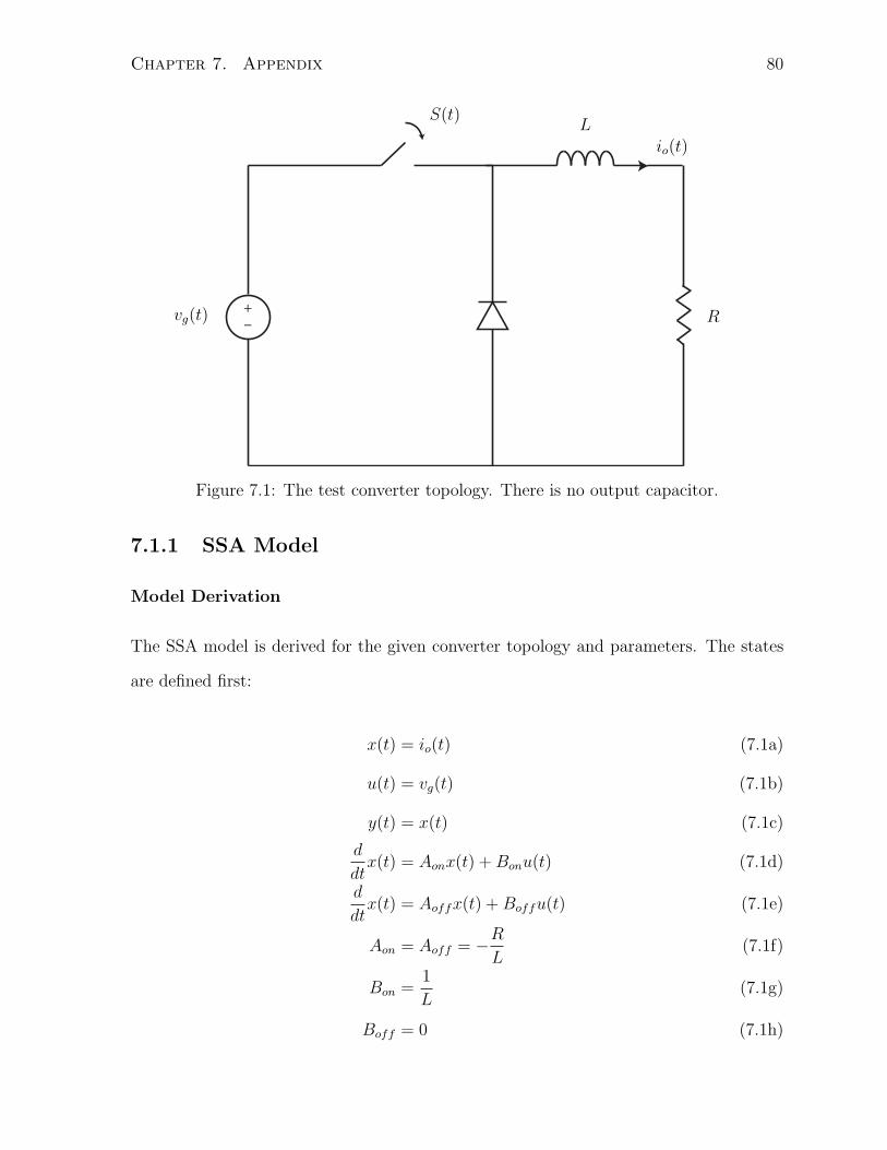
Chapter 7. Appendix 80
+
-vg(t)
L
R
io(t)
S(t)
Figure 7.1: The test converter topology. There is no output capacitor.
7.1.1 SSA Model
Model Derivation
The SSA model is derived for the given converter topology and parameters. The states
are defined first:
x(t) = io(t) (7.1a)
u(t) = vg(t) (7.1b)
y(t) = x(t) (7.1c)
d
dtx(t) = Aonx(t) +Bonu(t) (7.1d)
d
dtx(t) = Aoffx(t) + Boffu(t) (7.1e)
Aon = Aoff = −R
L(7.1f)
Bon =1
L(7.1g)
Boff = 0 (7.1h)

Chapter 7. Appendix 81
Based on the operating point let:
A = DAon + (1−D)Aoff (7.2a)
B = DBon + (1−D)Boff (7.2b)
C = DCon + (1−D)Coff (7.2c)
The linearized, small-signal model is then written as:
d
dtx(t) = Ax(t) + Bu(t) + [(Aon − Aoff )X + (Bon − Boff )U ] d(t) (7.3a)
y(t) = Cx(t) + Eu(t) + [(Con − Coff )X + (Eon − Eoff )U ] d(t) (7.3b)
After evaluating all parameters the system can be written as:
d
dtx(t) = −10000x(t)2000u(t) + 40000d(t) (7.4a)
y(t) = x(t) (7.4b)
7.2 Capless Buck Conveter with Motor Load
Consider a buck converter with no capacitor, and a motor load (constant voltage) as
shown in Figure 7.2.
The parameters of the circuit are established (and T = 1Fsw
) in Table 7.2. The
objective is be the control of the output current. The modelling approach will be based
upon this goal.

Chapter 7. Appendix 82
+
-
+
-vg(t)
L
vo(t)
io(t)
S(t)
Figure 7.2: The test converter topology. There is no output capacitor.
7.2.1 New Model
Model Derivation
The procedure outlined in Section 3.1 is followed for the derivation of the new model for
the shown topology. Let:
x(t) =
⎡
⎢
⎢
⎢
⎢
⎢
⎢
⎢
⎣
io(t)
iav(t)
vg(t)
vo(t)
⎤
⎥
⎥
⎥
⎥
⎥
⎥
⎥
⎦
(7.5)
where iav(t) represents the augmented SWA state. Then the dynamics are given as:
x(
(k + 1)T)
= eAoff
(
1−d(t))
T eAond(t)Tx(t) (7.6)

Chapter 7. Appendix 83
Table 7.2: Circuit Parameters
Parameter Value
Vg 10 V
Vo 5 V
Fsw 50 kHz
wsw 2π 50 000 rad/s
L 0.25 mH
D 0.5
where:
Aon =
⎡
⎢
⎢
⎢
⎢
⎢
⎢
⎢
⎣
0 0 1L
− 1L
1T
0 0 0
0 0 0 0
0 0 0 0
⎤
⎥
⎥
⎥
⎥
⎥
⎥
⎥
⎦
(7.7)
Aoff =
⎡
⎢
⎢
⎢
⎢
⎢
⎢
⎢
⎣
0 0 0 − 1L
1T
0 0 0
0 0 0 0
0 0 0 0
⎤
⎥
⎥
⎥
⎥
⎥
⎥
⎥
⎦
(7.8)
In discrete form:
x[k + 1] = Φ[k]x[k] (7.9)
This system describes the exact dynamics of the circuit. It is therefore referred to as the
exact switching model. The system is linearzied around the operating point (Table 7.2).
The final results are:
x [k + 1] = Adx [k] +Bd [k] (7.10a)
y [k] = Cx [k] (7.10b)

Chapter 7. Appendix 84
Ad =
⎡
⎢
⎢
⎢
⎢
⎢
⎢
⎢
⎣
1 0 0.04 −0.08
1 0 0.03 −0.04
0 0 1 0
0 0 0 1
⎤
⎥
⎥
⎥
⎥
⎥
⎥
⎥
⎦
(7.10c)
Bd =
⎡
⎢
⎢
⎢
⎢
⎢
⎢
⎢
⎣
0.8
0.4
0
0
⎤
⎥
⎥
⎥
⎥
⎥
⎥
⎥
⎦
(7.10d)
Cd =
[
0 1 0 0
]
(7.10e)
x = x[k]−X (7.10f)
There are couple remarks to be made. First, the SWA state was augmented as a second
state, and not at the end. This will be make things easier when designing the controller,
especially for pole placement. On point, the last states, the voltage input and output
are really not states in the sense they can be controlled. They will be excluded from the
feedback control. They’re included here in order to derive the full system dynamics and
because the input voltage is actually needed for the estimator design.
Controller Design
For the controller design a root locus method is used. The system in (7.10) can be written
as a discrete time transfer function:
P (z) =2(z + 1)
5(z)(z − 1)(7.11)
This transfer function can be used in a root locus design method. With a digital

Chapter 7. Appendix 85
+-
IrefC(z) P (z)
io[k]
d[k]
Figure 7.3: The closed loop structure for the given example. Plant and controller are allin discrete time. The output of the plant is the sampled average output current.
controller, the feedback is presented in Figure 7.3. The closed loop transfer function is:
T (z) =P (z)C(z)
1 + P (z)C(z)(7.12)
The controller will be a PI. As such its transfer function is:
C(z) = Kp +Ki
z − 1(7.13)
Since the pole is fixed for a PI controller, the only design choice is the placement of the
closed loop zero and the associated controller gains.
Figure 7.4 shows the root locus plot of the closed loop for a chosen controller. Unlike
continuous time root locus design, the goal is to ensure all closed loop poles are inside
the unit circle. Suitably, a zero has been placed at 0.8 on the real axis. The complex
conjugate poles have been placed for a good damping performance. The final controller
transfer function is therefore given by:
C(z) = 1.86 +0.372
z − 1(7.14)
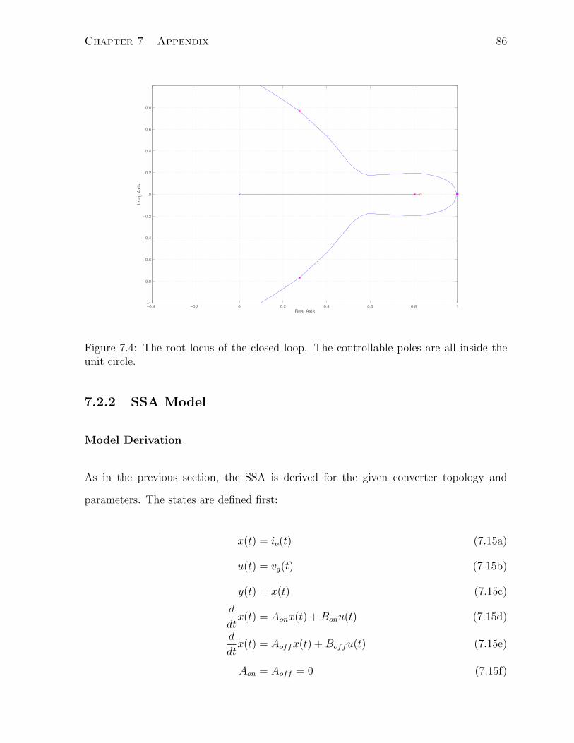
Chapter 7. Appendix 86
−0.4 −0.2 0 0.2 0.4 0.6 0.8 1−1
−0.8
−0.6
−0.4
−0.2
0
0.2
0.4
0.6
0.8
1
Real Axis
Imag
Axi
s
Figure 7.4: The root locus of the closed loop. The controllable poles are all inside theunit circle.
7.2.2 SSA Model
Model Derivation
As in the previous section, the SSA is derived for the given converter topology and
parameters. The states are defined first:
x(t) = io(t) (7.15a)
u(t) = vg(t) (7.15b)
y(t) = x(t) (7.15c)
d
dtx(t) = Aonx(t) +Bonu(t) (7.15d)
d
dtx(t) = Aoffx(t) + Boffu(t) (7.15e)
Aon = Aoff = 0 (7.15f)

Chapter 7. Appendix 87
Bon =1
L(7.15g)
Boff = 0 (7.15h)
Based on the operating point let:
A = DAon + (1−D)Aoff (7.16a)
B = DBon + (1−D)Boff (7.16b)
C = DCon + (1−D)Coff (7.16c)
The linearized, small-signal model is then written as:
d
dtx(t) = Ax(t) + Bu(t) + [(Aon − Aoff )X + (Bon − Boff )D] d(t) (7.17a)
y(t) = Cx(t) + Eu(t) + [(Con − Coff )X)D] d(t) (7.17b)
After evaluating all parameters the system can be written as:
d
dtx(t) = 2000u(t) + 40000d(t) (7.18a)
y(t) = x(t) (7.18b)
For this whole modelling to work, there needs to be a LPF that enacts the assump-
tions under which the model was derived. The LPF chosen is second order, with cutoff
frequency which is 13 (wn) of the switching frequency. Also its damping ratio is chosen
to be 0.7 (ζ) based on related in-lab testing. In other words, the transfer function of it:
LPF (s) =1
s2
wn+ 2ζ s
wn+ 1
(7.19)
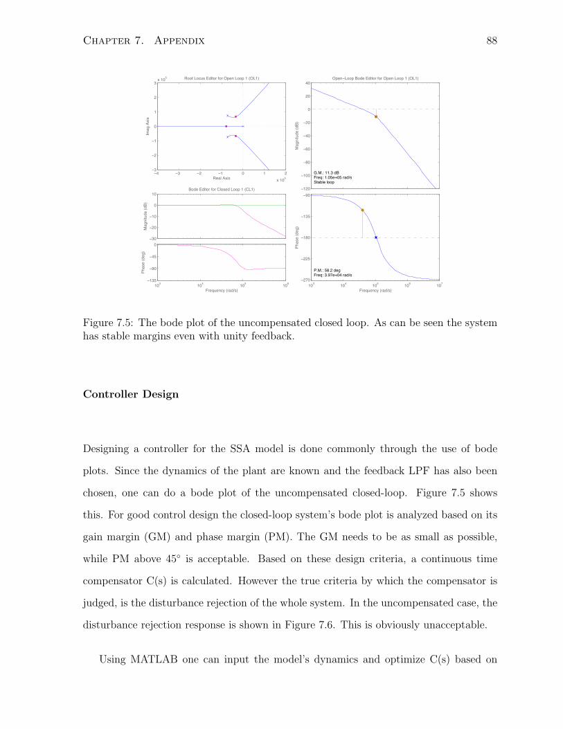
Chapter 7. Appendix 88
103 104 105 106−135
−90
−45
0
Frequency (rad/s)
Phas
e (d
eg)
−30
−20
−10
0
10Bode Editor for Closed Loop 1 (CL1)
Mag
nitu
de (d
B)
103 104 105 106 107−270
−225
−180
−135
−90
P.M.: 58.2 deg Freq: 3.97e+04 rad/s
Frequency (rad/s)Ph
ase
(deg
)
−120
−100
−80
−60
−40
−20
0
20
40
G.M.: 11.3 dB Freq: 1.05e+05 rad/sStable loop
Open−Loop Bode Editor for Open Loop 1 (OL1)
Mag
nitu
de (d
B)
−4 −3 −2 −1 0 1 2x 10⁵
−3
−2
−1
0
1
2
3x 10⁵ Root Locus Editor for Open Loop 1 (OL1)
Real Axis
Imag
Axi
s
Figure 7.5: The bode plot of the uncompensated closed loop. As can be seen the systemhas stable margins even with unity feedback.
Controller Design
Designing a controller for the SSA model is done commonly through the use of bode
plots. Since the dynamics of the plant are known and the feedback LPF has also been
chosen, one can do a bode plot of the uncompensated closed-loop. Figure 7.5 shows
this. For good control design the closed-loop system’s bode plot is analyzed based on its
gain margin (GM) and phase margin (PM). The GM needs to be as small as possible,
while PM above 45 is acceptable. Based on these design criteria, a continuous time
compensator C(s) is calculated. However the true criteria by which the compensator is
judged, is the disturbance rejection of the whole system. In the uncompensated case, the
disturbance rejection response is shown in Figure 7.6. This is obviously unacceptable.
Using MATLAB one can input the model’s dynamics and optimize C(s) based on

Chapter 7. Appendix 89
Step Response
Time (seconds)
Ampl
itude
0 0.5 1 1.5x 10⁻⁴
0
0.1
0.2
0.3
0.4
0.5
0.6
0.7
0.8
0.9
1
Figure 7.6: The output response to a step disturbance in the input. As it can be seenthe output never reaches zero steady state error - it settles to a steady state error.
having the best disturbance rejection. Doing this leads to the following compensator:
C(s) =16695 (1 + 9× 10⁻⁵s)
s(7.20)
Because the controller is being impemented digitally, the above compensator is dis-
cretized, with sample rate equal to the switching frequency:
C(z) =1.669z − 1.336
z − 1(7.21)
The new compensated disturbance rejection is shown in Figure 7.7.

Chapter 7. Appendix 90
Step Response
Time (seconds)
Am
plit
ud
e
0 0.5 1 1.5 2 2.5 3 3.5 4 4.5 5
x 10−4
0
0.1
0.2
0.3
0.4
0.5
0.6
0.7
Figure 7.7: The step response for the newly compensated system. The output returns tozero steady state error withing 0.4 ms.

Bibliography
[1] R. W. Brockett and J. R. Wood. Electrical networks containing controlled switches.
NASA STI/Recon Technical Report N, 75:18905, June 1974.
[2] Jingquan Chen, A Prodic, R.W. Erickson, and D. Maksimovic. Predictive digital
current programmed control. Power Electronics, IEEE Transactions on, 18(1):411–
419, Jan 2003.
[3] J. D’Azzo and C. Houpis. Linear Control System Analysis and Design: Conventional
and Modern. Mcgraw-Hill College Division, 1995.
[4] A De Castro, P. Zumel, O. Garcia, T. Riesgo, and J. Uceda. Concurrent and simple
digital controller of an ac/dc converter with power factor correction based on an
fpga. Power Electronics, IEEE Transactions on, 18(1):334–343, Jan 2003.
[5] R. W. Erickson, S. Cuk, and R. D. Middlebrook. Large-scale modelling and analysis
of switching regulators. NASA STI/Recon Technical Report N, 75:18905, June 1974.
[6] Robert W. Erickson. Fundamentals of Power Electronics. BS Publications, 2004.
[7] Huey Chian Foong, Meng Tong Tan, and Yuanjin Zheng. Predictive proportional
integral controller for digital dc-dc converters. In Industrial Electronics and Appli-
cations (ICIEA), 2011 6th IEEE Conference on, pages 2380–2383, June 2011.
91

Bibliography 92
[8] P. A Gray and P.W. Lehn. Time-domain derived frequency-domain voltage source
converter model for harmonic analysis. In Harmonics and Quality of Power
(ICHQP), 2012 IEEE 15th International Conference on, pages 512–517, June 2012.
[9] F. Guinjoan, J. Calvente, A Poveda, and L. Martinez. Large-signal modeling and
simulation of switching dc-dc converters. Power Electronics, IEEE Transactions on,
12(3):485–494, May 1997.
[10] Y. S Lee. A systematic and unified approach to modeling switches in switch-mode
power supplies. Industrial Electronics, IEEE Transactions on, IE-32(4):445–448,
Nov 1985.
[11] P.W. Lehn. Exact modeling of the voltage source converter. Power Delivery, IEEE
Transactions on, 17(1):217–222, Jan 2002.
[12] P.W. Lehn. Direct harmonic analysis of the voltage source converter. Power Delivery,
IEEE Transactions on, 18(3):1034–1042, July 2003.
[13] D. Maksimovic, AM. Stankovic, V.J. Thottuvelil, and George C. Verghese. Modeling
and simulation of power electronic converters. Proceedings of the IEEE, 89(6):898–
912, Jun 2001.
[14] D. Maksimovic and R. Zane. Small-signal discrete-time modeling of digitally con-
trolled pwm converters. Power Electronics, IEEE Transactions on, 22(6):2552–2556,
Nov 2007.
[15] P.G. Maranesi and M. Riva. Automatic modeling of pwm dc-dc converters. Power
Electronics Letters, IEEE, 1(4):97–100, Dec 2003.
[16] D. Middlebrook and S. Cuk. Modelling and analysis methods for dc-to-dc switching
converters. Proc. of the IEE International Semiconductor Power Converter Confer-
ence, pages 90–111, 1977.

Bibliography 93
[17] R. D. Middlebrook and Slobodan Cuk. A general unified approach to modeling
switching-converter power stages. International Journal of Electronics, 42(6):521–
550, 1977.
[18] Daniel M. Mitchell. DC/DC Switching Regulator Analysis. Mcgraw-Hill, 1988.
[19] R. Naim, G. Weiss, and S. Ben-Yaakov. H infin; control applied to boost power
converters. Power Electronics, IEEE Transactions on, 12(4):677–683, Jul 1997.
[20] G. Nirgude, R. Tirumala, and N. Mohan. A new, large-signal average model for
single-switch dc-dc converters operating in both ccm and dcm. In Power Electronics
Specialists Conference, 2001. PESC. 2001 IEEE 32nd Annual, volume 3, pages 1736–
1741 vol. 3, 2001.
[21] Kanjilal P. P. Adaptive prediction and predictive control. Institution of Electrical
Engineers, 1995.
[22] L. Rossetto, G. Spiazzi, P. Tenti, B. Fabiano, and C. Licitra. Fast-response high-
quality rectifier with sliding mode control. Power Electronics, IEEE Transactions
on, 9(2):146–152, Mar 1994.
[23] S.R. Sanders and George C. Verghese. Synthesis of averaged circuit models for
switched power converters. In Circuits and Systems, 1990., IEEE International
Symposium on, pages 679–683 vol.1, May 1990.
[24] K.M. Smedley and Slobodan Cuk. One-cycle control of switching converters. In
Power Electronics Specialists Conference, 1991. PESC ’91 Record., 22nd Annual
IEEE, pages 888–896, Jun 1991.
[25] H. R. Visser and P. P J Van den Bosch. Modelling of periodically switching networks.
In Power Electronics Specialists Conference, 1991. PESC ’91 Record., 22nd Annual
IEEE, pages 67–73, Jun 1991.

Bibliography 94
[26] AF. Witulski and R.W. Erickson. Extension of state-space averaging to resonant
switches and beyond. Power Electronics, IEEE Transactions on, 5(1):98–109, Jan
1990.
[27] Yongchang Zhang, Qin Zhang, Zhengxi Li, and Yingchao Zhang. Comparative study
of model predictive current control and voltage oriented control for pwm rectifiers.
In Electrical Machines and Systems (ICEMS), 2013 International Conference on,
pages 2207–2212, Oct 2013.


![Combustion Theory and Modelling - Cornell UniversityDownloaded By: [Cornell University] At: 18:31 21 May 2008 Combustion Theory and Modelling Vol. 12, No. 3, June 2008, 529–544 Time-averaging](https://static.fdocuments.in/doc/165x107/5e8906533af8500a4319a78b/combustion-theory-and-modelling-cornell-university-downloaded-by-cornell-university.jpg)

![Advanced Statistical Tools for Modelling of … Statistical Tools for Modelling of Composition and Processing Parameters for Alloy Development ... [7]. This technique ...](https://static.fdocuments.in/doc/165x107/5aad97a17f8b9a9c2e8e8105/advanced-statistical-tools-for-modelling-of-statistical-tools-for-modelling.jpg)